JP4592967B2 - Light emitting device and electric appliance - Google Patents
Light emitting device and electric appliance Download PDFInfo
- Publication number
- JP4592967B2 JP4592967B2 JP2001023828A JP2001023828A JP4592967B2 JP 4592967 B2 JP4592967 B2 JP 4592967B2 JP 2001023828 A JP2001023828 A JP 2001023828A JP 2001023828 A JP2001023828 A JP 2001023828A JP 4592967 B2 JP4592967 B2 JP 4592967B2
- Authority
- JP
- Japan
- Prior art keywords
- light emitting
- electrode
- emitting layer
- light
- organic
- Prior art date
- Legal status (The legal status is an assumption and is not a legal conclusion. Google has not performed a legal analysis and makes no representation as to the accuracy of the status listed.)
- Expired - Fee Related
Links
- 238000004768 lowest unoccupied molecular orbital Methods 0.000 claims description 31
- 238000004770 highest occupied molecular orbital Methods 0.000 claims description 30
- 239000000126 substance Substances 0.000 claims description 28
- 239000011368 organic material Substances 0.000 claims description 19
- 230000005264 electron capture Effects 0.000 claims description 16
- 238000010893 electron trap Methods 0.000 claims description 15
- 230000005525 hole transport Effects 0.000 claims description 8
- 238000005036 potential barrier Methods 0.000 claims description 6
- 230000009471 action Effects 0.000 claims description 5
- 239000005416 organic matter Substances 0.000 claims description 3
- 239000010410 layer Substances 0.000 description 72
- 238000005401 electroluminescence Methods 0.000 description 65
- 239000010408 film Substances 0.000 description 53
- 230000006798 recombination Effects 0.000 description 18
- 238000005215 recombination Methods 0.000 description 18
- 230000000903 blocking effect Effects 0.000 description 17
- 239000000463 material Substances 0.000 description 16
- 238000000034 method Methods 0.000 description 14
- 239000000758 substrate Substances 0.000 description 13
- 238000002347 injection Methods 0.000 description 8
- 239000007924 injection Substances 0.000 description 8
- 230000005284 excitation Effects 0.000 description 7
- 239000000969 carrier Substances 0.000 description 6
- 239000011521 glass Substances 0.000 description 6
- 230000005524 hole trap Effects 0.000 description 6
- 239000004973 liquid crystal related substance Substances 0.000 description 6
- 239000004593 Epoxy Substances 0.000 description 5
- 239000004020 conductor Substances 0.000 description 4
- 239000011159 matrix material Substances 0.000 description 4
- PXHVJJICTQNCMI-UHFFFAOYSA-N Nickel Chemical compound [Ni] PXHVJJICTQNCMI-UHFFFAOYSA-N 0.000 description 3
- 229910052782 aluminium Inorganic materials 0.000 description 3
- XAGFODPZIPBFFR-UHFFFAOYSA-N aluminium Chemical compound [Al] XAGFODPZIPBFFR-UHFFFAOYSA-N 0.000 description 3
- 230000007246 mechanism Effects 0.000 description 3
- 230000008569 process Effects 0.000 description 3
- 239000000565 sealant Substances 0.000 description 3
- RYGMFSIKBFXOCR-UHFFFAOYSA-N Copper Chemical compound [Cu] RYGMFSIKBFXOCR-UHFFFAOYSA-N 0.000 description 2
- 229910052581 Si3N4 Inorganic materials 0.000 description 2
- XUIMIQQOPSSXEZ-UHFFFAOYSA-N Silicon Chemical compound [Si] XUIMIQQOPSSXEZ-UHFFFAOYSA-N 0.000 description 2
- BQCADISMDOOEFD-UHFFFAOYSA-N Silver Chemical compound [Ag] BQCADISMDOOEFD-UHFFFAOYSA-N 0.000 description 2
- XLOMVQKBTHCTTD-UHFFFAOYSA-N Zinc monoxide Chemical compound [Zn]=O XLOMVQKBTHCTTD-UHFFFAOYSA-N 0.000 description 2
- 239000000956 alloy Substances 0.000 description 2
- 229910045601 alloy Inorganic materials 0.000 description 2
- 230000015572 biosynthetic process Effects 0.000 description 2
- 239000000919 ceramic Substances 0.000 description 2
- 238000006243 chemical reaction Methods 0.000 description 2
- 150000001875 compounds Chemical class 0.000 description 2
- 230000001747 exhibiting effect Effects 0.000 description 2
- 239000007850 fluorescent dye Substances 0.000 description 2
- PCHJSUWPFVWCPO-UHFFFAOYSA-N gold Chemical compound [Au] PCHJSUWPFVWCPO-UHFFFAOYSA-N 0.000 description 2
- 229910003437 indium oxide Inorganic materials 0.000 description 2
- PJXISJQVUVHSOJ-UHFFFAOYSA-N indium(iii) oxide Chemical compound [O-2].[O-2].[O-2].[In+3].[In+3] PJXISJQVUVHSOJ-UHFFFAOYSA-N 0.000 description 2
- 238000002161 passivation Methods 0.000 description 2
- 239000004033 plastic Substances 0.000 description 2
- 229920003023 plastic Polymers 0.000 description 2
- 229920003227 poly(N-vinyl carbazole) Polymers 0.000 description 2
- 229920005989 resin Polymers 0.000 description 2
- 239000011347 resin Substances 0.000 description 2
- 239000010703 silicon Substances 0.000 description 2
- 229910052710 silicon Inorganic materials 0.000 description 2
- HQVNEWCFYHHQES-UHFFFAOYSA-N silicon nitride Chemical compound N12[Si]34N5[Si]62N3[Si]51N64 HQVNEWCFYHHQES-UHFFFAOYSA-N 0.000 description 2
- 239000002356 single layer Substances 0.000 description 2
- 238000007740 vapor deposition Methods 0.000 description 2
- UHXOHPVVEHBKKT-UHFFFAOYSA-N 1-(2,2-diphenylethenyl)-4-[4-(2,2-diphenylethenyl)phenyl]benzene Chemical compound C=1C=C(C=2C=CC(C=C(C=3C=CC=CC=3)C=3C=CC=CC=3)=CC=2)C=CC=1C=C(C=1C=CC=CC=1)C1=CC=CC=C1 UHXOHPVVEHBKKT-UHFFFAOYSA-N 0.000 description 1
- YLYPIBBGWLKELC-RMKNXTFCSA-N 2-[2-[(e)-2-[4-(dimethylamino)phenyl]ethenyl]-6-methylpyran-4-ylidene]propanedinitrile Chemical compound C1=CC(N(C)C)=CC=C1\C=C\C1=CC(=C(C#N)C#N)C=C(C)O1 YLYPIBBGWLKELC-RMKNXTFCSA-N 0.000 description 1
- ZNJRONVKWRHYBF-VOTSOKGWSA-N 4-(dicyanomethylene)-2-methyl-6-julolidyl-9-enyl-4h-pyran Chemical compound O1C(C)=CC(=C(C#N)C#N)C=C1\C=C\C1=CC(CCCN2CCC3)=C2C3=C1 ZNJRONVKWRHYBF-VOTSOKGWSA-N 0.000 description 1
- WHXSMMKQMYFTQS-UHFFFAOYSA-N Lithium Chemical compound [Li] WHXSMMKQMYFTQS-UHFFFAOYSA-N 0.000 description 1
- FYYHWMGAXLPEAU-UHFFFAOYSA-N Magnesium Chemical compound [Mg] FYYHWMGAXLPEAU-UHFFFAOYSA-N 0.000 description 1
- NRCMAYZCPIVABH-UHFFFAOYSA-N Quinacridone Chemical compound N1C2=CC=CC=C2C(=O)C2=C1C=C1C(=O)C3=CC=CC=C3NC1=C2 NRCMAYZCPIVABH-UHFFFAOYSA-N 0.000 description 1
- VYPSYNLAJGMNEJ-UHFFFAOYSA-N Silicium dioxide Chemical compound O=[Si]=O VYPSYNLAJGMNEJ-UHFFFAOYSA-N 0.000 description 1
- PNEYBMLMFCGWSK-UHFFFAOYSA-N aluminium oxide Inorganic materials [O-2].[O-2].[O-2].[Al+3].[Al+3] PNEYBMLMFCGWSK-UHFFFAOYSA-N 0.000 description 1
- GQVWHWAWLPCBHB-UHFFFAOYSA-L beryllium;benzo[h]quinolin-10-olate Chemical compound [Be+2].C1=CC=NC2=C3C([O-])=CC=CC3=CC=C21.C1=CC=NC2=C3C([O-])=CC=CC3=CC=C21 GQVWHWAWLPCBHB-UHFFFAOYSA-L 0.000 description 1
- 238000004061 bleaching Methods 0.000 description 1
- 230000008859 change Effects 0.000 description 1
- 238000000576 coating method Methods 0.000 description 1
- 238000010276 construction Methods 0.000 description 1
- 229910052802 copper Inorganic materials 0.000 description 1
- 239000010949 copper Substances 0.000 description 1
- 239000011889 copper foil Substances 0.000 description 1
- 239000011162 core material Substances 0.000 description 1
- VBVAVBCYMYWNOU-UHFFFAOYSA-N coumarin 6 Chemical compound C1=CC=C2SC(C3=CC4=CC=C(C=C4OC3=O)N(CC)CC)=NC2=C1 VBVAVBCYMYWNOU-UHFFFAOYSA-N 0.000 description 1
- 230000008878 coupling Effects 0.000 description 1
- 238000010168 coupling process Methods 0.000 description 1
- 238000005859 coupling reaction Methods 0.000 description 1
- 230000009849 deactivation Effects 0.000 description 1
- 230000003247 decreasing effect Effects 0.000 description 1
- 230000006866 deterioration Effects 0.000 description 1
- 238000007598 dipping method Methods 0.000 description 1
- 230000000694 effects Effects 0.000 description 1
- 239000003822 epoxy resin Substances 0.000 description 1
- 230000005281 excited state Effects 0.000 description 1
- 239000011888 foil Substances 0.000 description 1
- 229910052737 gold Inorganic materials 0.000 description 1
- 239000010931 gold Substances 0.000 description 1
- 229910052744 lithium Inorganic materials 0.000 description 1
- 238000004020 luminiscence type Methods 0.000 description 1
- 229910052749 magnesium Inorganic materials 0.000 description 1
- 239000011777 magnesium Substances 0.000 description 1
- 229910052751 metal Inorganic materials 0.000 description 1
- 239000002184 metal Substances 0.000 description 1
- 239000002923 metal particle Substances 0.000 description 1
- 229910052759 nickel Inorganic materials 0.000 description 1
- 230000003287 optical effect Effects 0.000 description 1
- 239000013307 optical fiber Substances 0.000 description 1
- BPUBBGLMJRNUCC-UHFFFAOYSA-N oxygen(2-);tantalum(5+) Chemical compound [O-2].[O-2].[O-2].[O-2].[O-2].[Ta+5].[Ta+5] BPUBBGLMJRNUCC-UHFFFAOYSA-N 0.000 description 1
- 230000000737 periodic effect Effects 0.000 description 1
- 125000002080 perylenyl group Chemical group C1(=CC=C2C=CC=C3C4=CC=CC5=CC=CC(C1=C23)=C45)* 0.000 description 1
- CSHWQDPOILHKBI-UHFFFAOYSA-N peryrene Natural products C1=CC(C2=CC=CC=3C2=C2C=CC=3)=C3C2=CC=CC3=C1 CSHWQDPOILHKBI-UHFFFAOYSA-N 0.000 description 1
- 239000002985 plastic film Substances 0.000 description 1
- 229920006255 plastic film Polymers 0.000 description 1
- 229920000647 polyepoxide Polymers 0.000 description 1
- -1 polyparaphenylene vinylene Polymers 0.000 description 1
- 238000002360 preparation method Methods 0.000 description 1
- 238000007639 printing Methods 0.000 description 1
- 230000002250 progressing effect Effects 0.000 description 1
- 230000001681 protective effect Effects 0.000 description 1
- YYMBJDOZVAITBP-UHFFFAOYSA-N rubrene Chemical compound C1=CC=CC=C1C(C1=C(C=2C=CC=CC=2)C2=CC=CC=C2C(C=2C=CC=CC=2)=C11)=C(C=CC=C2)C2=C1C1=CC=CC=C1 YYMBJDOZVAITBP-UHFFFAOYSA-N 0.000 description 1
- 229910052814 silicon oxide Inorganic materials 0.000 description 1
- 229910052709 silver Inorganic materials 0.000 description 1
- 239000004332 silver Substances 0.000 description 1
- 229910000679 solder Inorganic materials 0.000 description 1
- 238000004528 spin coating Methods 0.000 description 1
- 238000004544 sputter deposition Methods 0.000 description 1
- 229910001936 tantalum oxide Inorganic materials 0.000 description 1
- 239000010409 thin film Substances 0.000 description 1
- XOLBLPGZBRYERU-UHFFFAOYSA-N tin dioxide Chemical compound O=[Sn]=O XOLBLPGZBRYERU-UHFFFAOYSA-N 0.000 description 1
- 229910001887 tin oxide Inorganic materials 0.000 description 1
- TVIVIEFSHFOWTE-UHFFFAOYSA-K tri(quinolin-8-yloxy)alumane Chemical compound [Al+3].C1=CN=C2C([O-])=CC=CC2=C1.C1=CN=C2C([O-])=CC=CC2=C1.C1=CN=C2C([O-])=CC=CC2=C1 TVIVIEFSHFOWTE-UHFFFAOYSA-K 0.000 description 1
- ODHXBMXNKOYIBV-UHFFFAOYSA-N triphenylamine Chemical class C1=CC=CC=C1N(C=1C=CC=CC=1)C1=CC=CC=C1 ODHXBMXNKOYIBV-UHFFFAOYSA-N 0.000 description 1
- 239000011787 zinc oxide Substances 0.000 description 1
Images


Landscapes
- Electroluminescent Light Sources (AREA)
- Devices For Indicating Variable Information By Combining Individual Elements (AREA)
Description
【0001】
【発明の属する技術分野】
本発明は、発光性有機膜を用いた発光装置に関する。また、その発光装置を表示部もしくは光源として用いた電気器具に関する。なお、本発明に用いることのできる発光性有機膜は、一重項励起もしくは三重項励起または両者の励起を経由して発光(燐光および/または蛍光)するすべての有機膜を含む。
【0002】
【従来の技術】
近年、EL(Electro Luminescence)が得られる発光性有機膜(以下、有機EL膜という)を利用した発光素子(以下、EL素子という)を用いた発光装置(以下、EL発光装置という)の開発が進んでいる。EL発光装置は、陽極と陰極との間に有機EL膜を挟んだ構造からなるEL素子を有し、陽極と陰極との間に電圧を加えることで発光を得る。
【0003】
このとき、陽極からは正孔(ホール)がEL材料中へ注入され、陰極からは電子(エレクトロン)が有機EL膜へ注入される。互いの電極から注入された電荷(キャリア)は有機EL膜内部を移動して再結合する。再結合することによって励起状態が生成され、そのうちの一部が光子に変換される。この光子が外部に取り出されることで発光として視認することができる。
【0004】
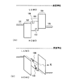
このような従来の発光機構を図2(A)、(B)に示す。図2(A)は従来のEL素子の接合構造であり、201は陰極(Cathode)、202は電子輸送層(Electron Transfer Layer)、203は発光層(Emission Layer)、204は正孔輸送層(Hole Transfer Layer)、205は陽極(Anode)である。また、図2(B)はそのキャリア注入過程であり、陰極201と陽極205との間に電圧が印加されることで電子206及び正孔207が注入されて再結合し、発光が得られる。
【0005】
このような発光機構を考えると、EL素子から発せられる光の効率、即ち発光効率(η(発光)と表す)は次式のように表される。
η(発光)=η(注入)×η(再結合)×η(励起)×η(量子)
ここでη(注入)はキャリアが電極から注入される際の効率、η(再結合)は電子及び正孔が再結合する効率、η(励起)は再結合により一重項励起子が生成する効率、η(量子)は一重項励起子から光子に変換される効率である。
【0006】
η(注入)は陰極(もしくは陽極)とEL材料との界面における電位障壁に起因して変化し、電位障壁が低いほど効率は高い。また、η(再結合)はキャリアの注入バランス(注入された電子及び正孔の割合のバランス)により変化し、発光層(実際に発光する有機EL膜)のキャリア輸送特性に影響される。また、η(励起)は発光に寄与する一重項励起子の生成効率であり、理論上は約0.25と決まっている。また、η(量子)は発光層が結晶質か非晶質かによって変化し、総じて結晶質の方が高い値が得られる。
【0007】
さらに、発光層中で生成された光子は外部に取り出されるまでに散乱や熱失活により殆どが失われる(約80%が失われる)ため、実際に観測される光はその分の損失も含めたものとなる。以上のように、EL素子の発光機構の過程では様々な要因により発光効率が低下してしまう。高い発光効率を得るには、上記の様々な効率を高め、総合的に高い発光効率を求めるしかない。
【0008】
【発明が解決しようとする課題】
本発明はEL素子におけるキャリアの再結合効率を高めるための手段を提供することを課題とし、発光効率の高い発光装置を提供することを課題とする。また、そのような発光装置を表示部もしくは光源として用いた電気器具を提供することを課題とする。
【0009】
【課題を解決するための手段】
本発明は、電子及び正孔の再結合効率(η(再結合)と表す)を改善するためにEL素子のバンド構造に着目し、特定の領域に電子及び正孔を閉じ込めることで再結合する確率を増加させ、再結合効率を高めることを特徴とする。そのために、図1(A)に示すようなバンド構造のEL素子を形成する。
【0010】
図1(A)において、101は陰極、102は電子輸送層、103は発光層、104は正孔輸送層、105は陽極である。また、発光層103の内部には、電子捕獲領域(Electron Trap Region)106、正孔捕獲領域(Hole Trap Region)107が形成される。なお、電子捕獲領域106と正孔捕獲領域107のどちらか片方が設けられた構造であっても良い。
【0011】
ここで、電子捕獲領域106は、発光層103の最低非占有分子軌道(LUMO)準位を輸送されてきた電子を発光層内に閉じ込める作用を有する領域であり、発光層103のLUMO準位よりも低いLUMO準位を示す領域を指す。また、正孔捕獲領域107は、発光層103の最高占有分子軌道(HOMO)準位を輸送されてきた正孔を発光層内に閉じ込める作用を有する領域であり、発光層103のHOMO準位よりも高いHOMO準位を示す領域を指す。
【0012】
電子捕獲領域106は、発光層103の間にLUMO準位を低くくするように作用する有機膜や有機物のクラスターを挟んだ構造とすることで形成できる。また、正孔捕獲領域107は、発光層103の間にHOMO準位を高くするように作用する有機膜や有機物のクラスターを挟んだ構造とすることで形成できる。
【0013】
また、上記電子捕獲領域106もしくは正孔捕獲領域107を設けると同時に、電子輸送層102と発光層103との間に正孔阻止層を設けても良いし、発光層103と正孔輸送層104との間に電子阻止層を設けても良い。勿論、正孔阻止層と電子阻止層を両方設ける構造としても良い。
【0014】
図1(A)に示したようなバンド構造とすると、図1(B)に示すようなキャリア注入過程となる。即ち、LUMO準位を輸送されてきた電子108は発光層103の内部に設けられた電子捕獲領域106に閉じ込められる。一方でHOMO準位を輸送されてきた正孔109は正孔捕獲領域107に閉じ込められる。その結果、電子捕獲領域106と正孔捕獲領域107との間で電子108と正孔109の再結合が起こり、発光が得られる。
【0015】
このとき、本発明では電子もしくは正孔が捕獲領域に閉じ込められた状態で再結合が行われるため、再結合効率(η(再結合))を従来例よりも向上させることができる。発光層内部に準位の井戸を形成してキャリアを閉じ込めるという発想は従来なかった発想と言える。
【0016】
以上のように、本発明を実施することで発光効率に寄与するいくつかのパラメータのうち再結合に起因する効率(η(再結合))が向上し、EL素子の発光効率が向上する。従って、従来と同じ輝度を得るにもEL素子の駆動電圧を低く設定することができるため、発光装置の低消費電力化が図れる。さらに、駆動電圧を下げることで有機EL膜の劣化が抑制され信頼性が向上する。
【0017】
【発明の実施の形態】
本実施の形態では、図1(A)に示したバンド構造を得るためのEL素子の構造について図3を用いて説明する。図3(A)はアクティブマトリクス型発光装置の画素の断面構造を模式的に表している。
【0018】
図3(A)において、301は基板、302はTFT(薄膜トランジスタ)、303は画素電極であり、画素電極303はEL素子の陽極として機能する。基板301はガラス基板、プラスチック基板(プラスチックフィルムも含む)を用いれば良い。また、TFT302は如何なる構造のTFTを用いても良く、プレーナ型TFTや逆スタガ型TFTを用いることができる。また、画素電極303は仕事関数の大きい透明導電膜、代表的には酸化インジウムと酸化スズとの化合物膜もしくは酸化インジウムと酸化亜鉛との化合物膜を用いれば良い。
【0019】
次に、304は画素電極の段差にEL材料が形成されないようにするための絶縁膜であり、珪素を含む絶縁膜(酸化シリコン膜、酸化窒化シリコン膜もしくは窒化シリコン膜)または有機樹脂膜を用いることが可能である。
【0020】
また、有機EL層305は有機EL膜を単層で用いても積層して用いても良い。即ち、有機EL膜を単層で用いて発光層としても良いし、様々な有機膜を組み合わせて積層し、各々を正孔輸送層(正孔注入層も含む)、正孔阻止層、発光層、電子阻止層もしくは電子輸送層(電子注入層も含む)のいずれかとして機能させることも可能である。
【0021】
また、陰極306は仕事関数の小さい材料を用いることが好ましく、周期表の1族もしくは2族に属する元素を含む材料を用いる。代表的にはアルミニウムとリチウムとの合金膜、マグネシウムと銀との合金膜を用いれば良い。勿論、他のどのような組み合わせの導電膜を用いても良い。
【0022】
ここで、図3(A)において307で示される領域を拡大した構造を図3(B)に示す。本実施の形態において、有機EL層305は正孔輸送層308、発光層309、電子輸送層310で形成されている。さらに、発光層309は発光層309a、発光層309b、発光層309cの三層構造となっている。勿論、発光層309a、発光層309b及び発光層309cはすべて同一の有機EL膜である。さらに、発光層309aと発光層309bとの界面には有機物のクラスター311が形成され、発光層309bと発光層309cとの界面には有機物のクラスター312が形成される。
【0023】
ここで、有機物のクラスター311は正孔捕獲領域を形成し、有機物のクラスター312は電子捕獲領域を形成する。但し、材料を変えることで有機物のクラスター311で電子捕獲領域を形成し、有機物のクラスター312で正孔捕獲領域を形成することも可能である。
【0024】
ここで示した有機EL層305は蒸着法、塗布法(スピンコーティング法、ディップ法、LB法もしくはナイフエッジ法)または印刷法で形成すれば良い。但し、有機物のクラスター311、312は蒸着法により形成することが望ましい。また、有機物のクラスターは規則的に設けられていても不規則に設けられていても良い。さらに、平板状の形状であっても粒状の形状であっても良い。勿論、本発明は上記成膜方法に限定されるものではなく、図3(B)の構造を形成しうるならば如何なる成膜方法を用いても良い。
【0025】
本実施の形態のような構造からなる有機EL層を有したEL素子では、陽極303から注入された正孔が有機物のクラスター311に捕獲され、陰極306から注入された電子が有機物のクラスター312に捕獲される。これは有機物のクラスター311ではHOMO準位が高くなっており、有機物のクラスター312ではLUMO準位が低くなっているからである。
【0026】
従って、局部的なポテンシャル(エネルギー準位)の井戸に閉じ込められた電子及び正孔は高い効率で再結合し、EL素子全体の発光効率が向上する。その結果、消費電力が低く、信頼性の高い発光装置が得られる。
【0027】
なお、発光層309に蛍光物質を添加して発光中心を蛍光物質に移しても良い。また、カラー発色をさせる場合には、R(赤)、G(緑)、B(青)の三種類の発光層を画素ごとに並べて成膜しても良いし、白色発光の発光層にカラーフィルターを組み合わせても良い。さらに、青色発光の発光層に色変換層(CCM)とカラーフィルターを組み合わせても良い。また、フォトブリーチング法と呼ばれる技術(光照射より蛍光色素が劣化する現象を利用した技術)を用いることも可能である。
【0028】
また、本実施の形態ではTFTとEL素子とを電気的に接続させたアクティブマトリクス型発光装置を例に挙げたが、パッシブマトリクス型発光装置に本発明を実施しても構わない。また、液晶ディスプレイのバックライトもしくは蛍光表示灯のバックライトとなる光源として用いることも可能である。
【0029】
【実施例】
〔実施例1〕
本実施例では、図3(B)に示した有機物のクラスター311、312の代わりに有機膜を用いる場合の例を図4に示す。なお、発光装置の構造は図3(A)と同様である。
【0030】
本実施例では、電子捕獲領域を形成するためにLUMO準位を低くくするように作用する有機膜401もしくは正孔捕獲領域を形成するためにHOMO準位を高くするように作用する有機膜402を設けた構造とする点に特徴がある。有機膜401、402は両方とも設けても良いし、どちらか片方を設けても良い。また、有機膜401、402の膜厚は10〜50nm(好ましくは20〜30nm)とすれば良い。
【0031】
本実施例の構造とした場合においても、有機膜401で正孔が捕獲され、有機膜402で電子が捕獲されるため、再結合効率を向上させることができ、EL素子の駆動電圧を低くすることができる。即ち、消費電力が低く、信頼性の高い発光装置を得ることができる。
【0032】
〔実施例2〕
図3(B)に示した構造では、正孔捕獲領域となる有機物のクラスター311が陽極303側に設けられ、電子捕獲領域となる有機物のクラスター312が陰極306側に設けられた構造となっているが、この配置は逆でも良い。即ち、正孔捕獲領域となる有機物のクラスター311が陰極306側に設けられ、電子捕獲領域となる有機物のクラスター312が陽極303側に設けられた構造となっていても構わない。
【0033】
同様に、図4に示した構造において、正孔捕獲領域となる有機膜401が陰極306側に設けられ、電子捕獲領域となる有機膜402が陽極303側に設けられた構造となっていても構わない。
【0034】
〔実施例3〕
本実施例では、図1(A)と異なるバンド構造を有するEL素子を用いた発光装置について図5を用いて説明する。なお、図5において図1と異なる点は発光層500の部分だけなのでその他の部分は同一の符号を用いる。
【0035】
図5(A)に示す本実施例の構造は、発光層500の内部に電子捕獲領域501、正孔阻止領域502、正孔捕獲領域503及び電子阻止領域504が形成されている点に特徴がある。ここで正孔阻止領域とは、正孔109の陰極101側への移動を阻止する電位障壁となる領域であり、電子阻止領域とは電子108の陽極105側への移動を阻止する電位障壁となる領域である。
【0036】
本実施例では、電子捕獲領域501と正孔阻止領域502とが同一の有機物で形成され、正孔捕獲領域503と電子阻止領域504とが同一の有機物で形成される。同一の有機物とは有機膜もしくは有機物のクラスターであるが、本実施例ではLUMO準位及びHOMO準位を低くする作用を持つ有機物と、LUMO準位及びHOMO準位を高くする作用を持つ有機物とを用いる必要がある。その際、LUMO準位及びHOMO準位を低くする作用を持つ有機物により電子捕獲領域501及び正孔阻止領域502が形成され、LUMO準位及びHOMO準位を高くする作用を持つ有機物により正孔捕獲領域503及び電子阻止領域504が形成される。
【0037】
なお、本実施例では、発光層500の内部に電子捕獲領域501、正孔阻止領域502、正孔捕獲領域503及び電子阻止領域504の四つの領域が形成された例を示したが、いずれか一つまたはいずれか二つもしくは三つとしても良い。勿論、二つもしくは三つとする場合の組み合わせは自由である。
【0038】
本実施例の構造とすると、電極から注入されたキャリアは阻止領域に阻まれて発光層500の内部に留まるため、捕獲領域に閉じ込められる確率が向上し、延いては再結合効率(η(再結合))が向上する。その結果、EL素子の駆動電圧が下がり、発光装置の消費電力の低下、信頼性の向上が図れる。
【0039】
〔実施例4〕
本実施例では、図1(A)と異なるバンド構造を有するEL素子を用いた発光装置について図6を用いて説明する。なお、図6において図1と異なる点は発光層600の部分だけなのでその他の部分は同一の符号を用いる。
【0040】
図6(A)に示す本実施例の構造は、発光層600の内部に電子捕獲領域601及び正孔捕獲領域602が形成され、両者が同一の有機物で形成されている点に特徴がある。同一の有機物とは有機膜もしくは有機物のクラスターであるが、本実施例ではLUMO準位を低くし、且つ、HOMO準位を高くする作用を持つ有機物を用いる必要がある。
【0041】
本実施例の構造としたとき、電極から注入されたキャリアは同一層に形成された捕獲領域に閉じ込められるが、この場合にはLUMO準位とHOMO準位のバンドギャップが非常に小さくなるため再結合効率(η(再結合))が向上する。その結果、EL素子の駆動電圧が下がり、発光装置の消費電力の低下、信頼性の向上が図れる。
【0042】
〔実施例5〕
本実施例では、本願発明の発光装置の一例について図7を用いて説明する。なお、図7(A)は断面図、図7(B)は上面図である。
【0043】
図7(A)において、701は基板であり、その上に画素部702及び駆動回路703が形成されている。画素部702及び駆動回路703は配線704〜706によって電気信号の授受を行うことができる。基板701は可視光に対して透明であれば如何なる材料を用いても良い。
【0044】
画素部702にはTFT及びEL素子を含む複数の画素(典型的には図3(A)に示したような構造の画素)がマトリクス状に形成されており、その上にはパッシベーション膜707が形成されている。本実施例ではパッシベーション膜707として酸化タンタル膜をスパッタ法により形成しているが、有機EL膜を劣化させない温度で成膜可能であれば窒化シリコン膜を設けても良い。
【0045】
また、配線704、706の上にはエポキシ系樹脂からなるシール剤708が画素部702及び駆動回路703を囲むように形成され、シール剤708によってプリント配線板(PWB:Printed wiring board)709が貼り合わせてある。なお、プリント配線板の材質としては、典型的にはガラス布−エポキシ、エポキシ系フィルム、ガラス布−耐熱エポキシ、セラミックス、アルミナ、紙ベース−フェノールもしくは紙ベース−エポキシを用いることができる。また、ガラス基板、結晶化ガラス基板もしくはプラスチック基板を用いても良い。本実施例では、コア材にセラミックス710を用い、それをガラス布−エポキシ系基材711で挟んだプリント配線板を用いる。
【0046】
このとき、シール剤708の内部には異方導電性フィルム(代表的には、金属粒子を分散させた樹脂)もしくはメタルバンプ(代表的には、はんだバンプ、金バンプ、ニッケルバンプもしくは銅バンプ)からなる導電体712、713が設けられ、導電体712、713を介して配線704もしくは706とプリント配線板709に形成された配線群714とが電気的に接続されている。なお、ここでいう配線群とは、プリント配線板709の表面、裏面もしくは内部に形成されている配線の総称である。
【0047】
また、配線群714はFPC(Flexible Printed circuit)715に伝送されてきた電気信号を導電体712、713に伝送したり、プリント配線板709上に接続された様々なIC(集積回路)715、716の間で電気信号をやりとりするための配線であり、1〜20μmの厚さで形成されている。配線群714として、代表的には銅箔、金箔、銀箔、ニッケル箔もしくはアルミニウム箔からなるパターンが用いられる。
【0048】
以上のような構造を含む本実施例の発光装置は、FPC715に伝送されてきた電気信号をプリント配線板709で処理し、処理を行った電気信号を導電体712、713を介して画素部702もしくは駆動回路703に伝送する。このとき、本実施例ではプリント配線板709がEL素子を外的な衝撃から保護する保護板となっている。また、プリント配線板709はEL素子を閉空間に封入するための基板として用いることもできる。
【0049】
なお、本実施例ではプリント配線板709に信号処理機能を持たせるべくICを搭載した例を示したが、単に配線群のみを形成し、画素部702や駆動回路703で用いられる配線を低抵抗化するための冗長配線として用いることもできる。こうすることで、例えばEL素子に電流を供給する配線やTFTのゲート配線の信号遅延を改善することができる。
【0050】
以上のように、プリント配線板を発光装置の基板の一つとして用いることで発光装置の高性能化や高信頼性化が図れる。なお、本実施例の構成に実施例1〜4のいずれの構成を組み合わせて実施しても良い。
【0051】
〔実施例6〕
本実施例では、本発明に用いることができる有機EL膜について説明する。本発明の特徴は、発光層の内部にLUMO準位もしくはHOMO準位を局部的に変化させる有機物のクラスターや有機膜を設ける点にあり、この条件を満たすものであれば如何なる有機膜を用いても構わない。なお、三重項励起を経由して発光する有機物のクラスターもしくは有機膜を用いても構わない。
【0052】
具体的には、発光層としてAlq3(トリス−6−キノリラトアルミニウム錯体)、DPVBi(ジスチルアリーレン誘導体)、BeBq2(ビスベンゾキノリラトベリリウム錯体)、TPD(トリフェニルアミン誘導体)、α−NPD、PPV(ポリパラフェニレンビニレン)、PVK(ポリビニルカルバゾール)といった材料を用いることが可能である。ここで発光層として用いることのできる上記材料の分子構造を以下に示す。
【0053】
【化1】

【化2】
【化3】
【化4】
【化5】
【化6】
【化7】
また、具体的には、蛍光色素としてクマリン6、DCM1、DCM2、キナクリドン、ルブレンもしくはペリレンといった材料を用いることが可能である。ここで発光層として用いることのできる上記材料の分子構造を以下に示す。
【0061】
【化8】
【化9】
【化10】
【化11】
【化12】
上記発光層と蛍光物質を適切に組み合わせることで本発明のバンド構造を形成することが可能である。なお、本実施例の構成は実施例1〜6のいずれの構成とも自由に組み合わせることが可能である。
【0067】
〔実施例7〕
本発明を実施して作製された発光装置は様々な電気器具の表示部として用いることができる。例えば、TV放送等を大画面で鑑賞するには対角20〜60インチのディスプレイとして本発明の発光装置を筐体に組み込んだディスプレイを用いるとよい。なお、発光装置を筐体に組み込んだディスプレイには、パソコン用ディスプレイ、TV放送受信用ディスプレイ、広告表示用ディスプレイ等の全ての情報表示用ディスプレイが含まれる。
【0068】
また、液晶モジュール(液晶パネル)を筐体に組み込んだ液晶ディスプレイにおいて、バックライトの光源として本発明の発光装置を用いることも可能である。さらに、工事現場の蛍光表示灯などの光源として用いても良い。これら液晶ディスプレイや蛍光表示灯も電気器具である。
【0069】
また、その他にも様々な電気器具の表示部として本発明の発光装置を用いることができる。本発明の電気器具としては、ビデオカメラ、デジタルカメラ、ゴーグル型ディスプレイ(ヘッドマウントディスプレイ)、ナビゲーションシステム、音楽再生装置(代表的にはカーオーディオもしくはオーディオコンポーネント)、ノート型パーソナルコンピュータ、ゲーム機器、携帯情報端末(代表的にはモバイルコンピュータ、携帯電話、携帯型ゲーム機もしくは電子書籍)、画像再生装置(代表的には記録媒体に記録された画像を再生し、表示する表示部を備えた装置)が挙げられる。特に、斜め方向から見ることの多い携帯情報端末は視野角の広さが重要視されるため、発光装置を用いることが望ましい。それら電気器具の具体例を図8、図9に示す。
【0070】
図8(A)は発光装置を筐体に組み込んだディスプレイであり、筐体2001、支持台2002、表示部2003等を含む。本願発明は表示部2003に用いることができる。このようなディスプレイは発光型であるためバックライトが必要なく、液晶ディスプレイよりも薄い表示部とすることができる。
【0071】
図8(B)はビデオカメラであり、本体2101、表示部2102、音声入力部2103、操作スイッチ2104、バッテリー2105、受像部2106等を含む。本願発明の発光装置は表示部2102に用いることができる。
【0072】
図8(C)は頭部取り付け型のELディスプレイの一部(右片側)であり、本体2201、信号ケーブル2202、頭部固定バンド2203、表示部2204、光学系2205、発光装置2206等を含む。本願発明は発光装置2206に用いることができる。
【0073】
図8(D)は記録媒体を備えた画像再生装置(具体的にはDVD再生装置)であり、本体2301、記録媒体(DVD等)2302、操作スイッチ2303、表示部(a)2304、表示部(b)2305等を含む。表示部(a)は主として画像情報を表示し、表示部(b)は主として文字情報を表示するが、本願発明の発光装置はこれら表示部(a)、(b)に用いることができる。なお、記録媒体を備えた画像再生装置には家庭用ゲーム機器なども含まれる。
【0074】
図8(E)は携帯型(モバイル)コンピュータであり、本体2401、カメラ部2402、受像部2403、操作スイッチ2404、表示部2405等を含む。本願発明の発光装置は表示部2405に用いることができる。
【0075】
図8(F)はパーソナルコンピュータであり、本体2501、筐体2502、表示部2503、キーボード2504等を含む。本願発明の発光装置は表示部2503に用いることができる。
【0076】
なお、将来的に発光輝度がさらに高くなれば、出力した画像情報を含む光をレンズや光ファイバー等で拡大投影してフロント型若しくはリア型のプロジェクターに用いることも可能となる。
【0077】
また、発光装置は発光している部分が電力を消費するため、発光部分が極力少なくなるように情報を表示することが望ましい。従って、携帯情報端末、特に携帯電話や音響再生装置のような文字情報を主とする表示部に発光装置を用いる場合には、非発光部分を背景として文字情報を発光部分で形成するように駆動することが望ましい。
【0078】
ここで図9(A)は携帯電話であり、本体2601、音声出力部2602、音声入力部2603、表示部2604、操作スイッチ2605、アンテナ2606を含む。本願発明の発光装置は表示部2604に用いることができる。なお、表示部2604は黒色の背景に白色の文字を表示することで携帯電話の消費電力を抑えることができる。
【0079】
また、図9(B)は音楽再生装置、具体的にはカーオーディオであり、本体2701、表示部2702、操作スイッチ2703、2704を含む。本願発明の発光装置は表示部2702に用いることができる。また、本実施例ではカーオーディオを示すが、携帯型や家庭用の音響再生装置に用いても良い。なお、表示部2704は黒色の背景に白色の文字を表示することで消費電力を抑えられる。これは携帯型の音響再生装置において特に有効である。
【0080】
以上の様に、本願発明の適用範囲は極めて広く、あらゆる分野の電気器具に用いることが可能である。また、本実施例の電気器具は実施例1〜5に示したいずれの構成発光装置を用いても良い。
【0081】
〔実施例8〕
本発明の発光装置を表示部とする電気器具を屋外で使う場合、当然暗い所で見る場合も明るい所で見る場合もある。このとき、暗い所ではさほど輝度が高くなくても十分に認識できるが、明るい所では輝度が高くないと認識できない場合がありうる。EL発光装置の場合、輝度は素子を動作させる電流量に比例して変化するため、輝度を高くする場合は消費電力も増してしまう。しかし、発光輝度をそのような高いレベルに合わせてしまうと、暗い所では消費電力ばかり大きくで必要以上に明るい表示となってしまうことになる。
【0082】
そのような場合に備えて、本発明のEL発光装置もしくは電気器具に外部の明るさをセンサーで感知して、明るさの程度に応じて発光輝度を調節する機能を持たせることは有効である。即ち、明るい所では発光輝度を高くし、暗い所では発光輝度を低くする。その結果、消費電力の増加を防ぐとともに観測者に疲労感を与えないEL発光装置を実現することができる。
【0083】
なお、外部の明るさを感知するセンサーとしては、CMOSセンサーやCCD(チャージカップルドデバイス)を用いることができる。CMOSセンサーは公知の技術を用いてEL素子の形成された基板上に一体形成することもできるし、ICを外付けしても良い。また、CCDを形成したICをEL素子の形成された基板に取り付けても良いし、EL発光装置を表示部として用いた電気器具の一部にCCDやCMOSセンサーを設ける構造としても構わない。
【0084】
こうして外部の明るさを感知するセンサーによって得られた信号に応じて、発光素子を動作させる電流量を変えるための制御回路を設け、それにより外部の明るさに応じてEL素子の発光輝度を調節しうる。なお、このような調節は自動で行われるようにしても良いし、手動で行えるようにしても良い。
【0085】
本発明のEL発光装置もしくは電気器具に本実施例の構成を加えると、EL発光装置のさらなる低消費電力化を図ることが可能である。なお、本実施例の構成は、実施例7に示したどの電気器具においても実施することが可能である。
【0086】
【発明の効果】
本発明を実施することでEL素子の駆動電圧を下げることが可能となり、発光装置の低消費電力化及び高信頼性化(長寿命化)が図れる。さらには、本発明の発光装置を表示部に用いた電気器具の低消費電力化を図ることが可能となる。
【図面の簡単な説明】
【図1】EL素子のバンド構造を示す図。
【図2】EL素子のバンド構造を示す図。
【図3】EL発光装置の画素及びEL素子の断面構造を示す図。
【図4】EL素子の断面構造を示す図。
【図5】EL素子のバンド構造を示す図。
【図6】EL素子のバンド構造を示す図。
【図7】EL発光装置の断面構造を示す図。
【図8】電気器具の一例を示す図。
【図9】電気器具の一例を示す図。[0001]
BACKGROUND OF THE INVENTION
The present invention relates to a light emitting device using a light emitting organic film. The present invention also relates to an electric appliance using the light emitting device as a display unit or a light source. The light-emitting organic film that can be used in the present invention includes all organic films that emit light (phosphorescence and / or fluorescence) through singlet excitation, triplet excitation, or both excitation.
[0002]
[Prior art]
In recent years, there has been a development of a light emitting device (hereinafter referred to as an EL light emitting device) using a light emitting element (hereinafter referred to as an EL element) using a light emitting organic film (hereinafter referred to as an organic EL film) from which EL (Electro Luminescence) can be obtained. Progressing. The EL light emitting device has an EL element having a structure in which an organic EL film is sandwiched between an anode and a cathode, and obtains light emission by applying a voltage between the anode and the cathode.
[0003]
At this time, holes (holes) are injected into the EL material from the anode, and electrons (electrons) are injected into the organic EL film from the cathode. Charges (carriers) injected from each other electrode move inside the organic EL film and recombine. Recombination generates excited states, some of which are converted to photons. This photon is taken out to the outside and can be visually recognized as light emission.
[0004]
Such a conventional light emitting mechanism is shown in FIGS. FIG. 2A shows a junction structure of a conventional EL element, in which 201 is a cathode, 202 is an electron transport layer, 203 is a light emitting layer, and 204 is a hole transport layer. A hole transfer layer (205) is an anode. FIG. 2B shows the carrier injection process. When a voltage is applied between the
[0005]
Considering such a light emission mechanism, the efficiency of light emitted from the EL element, that is, the light emission efficiency (represented as η (light emission)) is expressed by the following equation.
η (luminescence) = η (injection) × η (recombination) × η (excitation) × η (quantum)
Here, η (injection) is the efficiency when carriers are injected from the electrode, η (recombination) is the efficiency with which electrons and holes are recombined, and η (excitation) is the efficiency with which singlet excitons are generated by recombination. , Η (quantum) is the efficiency of conversion from singlet excitons to photons.
[0006]
η (injection) changes due to a potential barrier at the interface between the cathode (or anode) and the EL material, and the lower the potential barrier, the higher the efficiency. Further, η (recombination) changes depending on the carrier injection balance (balance of the ratio of injected electrons and holes), and is influenced by the carrier transport property of the light emitting layer (the organic EL film that actually emits light). Further, η (excitation) is the generation efficiency of singlet excitons contributing to light emission, and is theoretically determined to be about 0.25. Further, η (quantum) varies depending on whether the light emitting layer is crystalline or amorphous, and as a whole, a higher value is obtained for crystalline.
[0007]
Furthermore, most of the photons generated in the light-emitting layer are lost due to scattering and thermal deactivation until they are extracted outside (approximately 80% is lost). It will be. As described above, in the process of the light emission mechanism of the EL element, the light emission efficiency is lowered due to various factors. In order to obtain a high luminous efficiency, there is no choice but to increase the above various efficiencies and to obtain a high luminous efficiency comprehensively.
[0008]
[Problems to be solved by the invention]
An object of the present invention is to provide a means for increasing the recombination efficiency of carriers in an EL element, and to provide a light emitting device with high light emission efficiency. It is another object of the present invention to provide an electric appliance using such a light-emitting device as a display unit or a light source.
[0009]
[Means for Solving the Problems]
The present invention focuses on the band structure of an EL element in order to improve the recombination efficiency (represented by η (recombination)) of electrons and holes, and recombines by confining electrons and holes in a specific region. It is characterized by increasing the probability and increasing the recombination efficiency. For this purpose, an EL element having a band structure as shown in FIG.
[0010]
In FIG. 1A, 101 is a cathode, 102 is an electron transport layer, 103 is a light emitting layer, 104 is a hole transport layer, and 105 is an anode. In addition, an
[0011]
Here, the
[0012]
The
[0013]
In addition, a hole blocking layer may be provided between the
[0014]
If the band structure is as shown in FIG. 1A, the carrier injection process is as shown in FIG. That is, the
[0015]
At this time, in the present invention, since recombination is performed in a state where electrons or holes are confined in the capture region, recombination efficiency (η (recombination)) can be improved as compared with the conventional example. The idea of confining carriers by forming a level well inside the light emitting layer can be said to have never existed before.
[0016]
As described above, by implementing the present invention, efficiency (η (recombination)) due to recombination among several parameters contributing to light emission efficiency is improved, and the light emission efficiency of the EL element is improved. Therefore, since the driving voltage of the EL element can be set low to obtain the same luminance as the conventional one, the power consumption of the light emitting device can be reduced. Further, by reducing the drive voltage, the deterioration of the organic EL film is suppressed and the reliability is improved.
[0017]
DETAILED DESCRIPTION OF THE INVENTION
In this embodiment, a structure of an EL element for obtaining the band structure shown in FIG. 1A will be described with reference to FIGS. FIG. 3A schematically illustrates a cross-sectional structure of a pixel of an active matrix light-emitting device.
[0018]
In FIG. 3A, reference numeral 301 denotes a substrate, 302 denotes a TFT (thin film transistor), 303 denotes a pixel electrode, and the
[0019]
Next,
[0020]
The
[0021]
The
[0022]
Here, FIG. 3B shows a structure in which the region indicated by
[0023]
Here, the
[0024]
The
[0025]
In an EL element having an organic EL layer having a structure as in this embodiment, an
[0026]
Therefore, electrons and holes confined in a well having a local potential (energy level) are recombined with high efficiency, and the light emission efficiency of the entire EL element is improved. As a result, a light-emitting device with low power consumption and high reliability can be obtained.
[0027]
Note that a fluorescent material may be added to the light-emitting
[0028]
Further, although an active matrix light-emitting device in which a TFT and an EL element are electrically connected is described as an example in this embodiment, the present invention may be implemented in a passive matrix light-emitting device. Further, it can also be used as a light source for a backlight of a liquid crystal display or a backlight of a fluorescent display lamp.
[0029]
【Example】
[Example 1]
In this embodiment, an example in which an organic film is used instead of the
[0030]
In this embodiment, the
[0031]
Even in the case of the structure of this embodiment, holes are captured by the
[0032]
[Example 2]
In the structure shown in FIG. 3B, an
[0033]
Similarly, in the structure shown in FIG. 4, the
[0034]
Example 3
In this example, a light-emitting device using an EL element having a band structure different from that in FIG. 1A will be described with reference to FIGS. 5 is different from FIG. 1 only in the
[0035]
The structure of this embodiment shown in FIG. 5A is characterized in that an
[0036]
In this embodiment, the
[0037]
Note that in this embodiment, an example in which four regions of the
[0038]
With the structure of this embodiment, carriers injected from the electrode are blocked by the blocking region and remain inside the
[0039]
Example 4
In this example, a light-emitting device using an EL element having a band structure different from that in FIG. 1A will be described with reference to FIGS. 6 is different from FIG. 1 only in the
[0040]
The structure of this embodiment shown in FIG. 6A is characterized in that an
[0041]
In the structure of this embodiment, carriers injected from the electrode are confined in the trap region formed in the same layer. In this case, the band gap between the LUMO level and the HOMO level becomes very small, so Coupling efficiency (η (recombination)) is improved. As a result, the driving voltage of the EL element is reduced, and the power consumption of the light emitting device is reduced and the reliability is improved.
[0042]
Example 5
In this example, an example of a light-emitting device of the present invention will be described with reference to FIG. 7A is a cross-sectional view, and FIG. 7B is a top view.
[0043]
In FIG. 7A,
[0044]
In the
[0045]
A
[0046]
At this time, an anisotropic conductive film (typically a resin in which metal particles are dispersed) or a metal bump (typically a solder bump, a gold bump, a nickel bump, or a copper bump) is placed inside the
[0047]
The
[0048]
In the light emitting device of this embodiment including the above-described structure, the electrical signal transmitted to the
[0049]
In this embodiment, an example is shown in which an IC is mounted on the printed
[0050]
As described above, by using the printed wiring board as one of the substrates of the light emitting device, high performance and high reliability of the light emitting device can be achieved. In addition, you may implement combining the structure of a present Example in any structure of Examples 1-4.
[0051]
Example 6
In this example, an organic EL film that can be used in the present invention will be described. The feature of the present invention is that an organic material cluster or an organic film for locally changing the LUMO level or the HOMO level is provided inside the light emitting layer, and any organic film that satisfies this condition can be used. It doesn't matter. Note that an organic substance cluster or an organic film that emits light through triplet excitation may be used.
[0052]
Specifically, Alq3 (tris-6-quinolinolato aluminum complex), DPVBi (distilarylene derivative), BeBq2 (bisbenzoquinolinatoberyllium complex), TPD (triphenylamine derivative), α- Materials such as NPD, PPV (polyparaphenylene vinylene), and PVK (polyvinylcarbazole) can be used. Here, the molecular structure of the above material that can be used as the light emitting layer is shown below.
[0053]
[Chemical 1]
[Chemical 2]
[Chemical 3]
[Formula 4]
[Chemical formula 5]
[Chemical 6]
[Chemical 7]
Specifically, a material such as coumarin 6, DCM1, DCM2, quinacridone, rubrene, or perylene can be used as the fluorescent dye. Here, the molecular structure of the above material that can be used as the light emitting layer is shown below.
[0061]
[Chemical 8]
[Chemical 9]
[Chemical Formula 10]
Embedded image
Embedded image
The band structure of the present invention can be formed by appropriately combining the light emitting layer and the fluorescent material. In addition, the structure of a present Example can be freely combined with any structure of Examples 1-6.
[0067]
Example 7
A light-emitting device manufactured by implementing the present invention can be used as a display portion of various electric appliances. For example, in order to watch TV broadcasting or the like on a large screen, a display in which the light-emitting device of the present invention is incorporated in a housing may be used as a diagonal display of 20 to 60 inches. Note that the display in which the light emitting device is incorporated in the housing includes all information display displays such as a personal computer display, a TV broadcast reception display, and an advertisement display.
[0068]
In a liquid crystal display in which a liquid crystal module (liquid crystal panel) is incorporated in a housing, the light emitting device of the present invention can be used as a light source of a backlight. Furthermore, it may be used as a light source such as a fluorescent lamp at a construction site. These liquid crystal displays and fluorescent lamps are also electric appliances.
[0069]
In addition, the light-emitting device of the present invention can be used as a display portion of various electric appliances. The electric appliance of the present invention includes a video camera, a digital camera, a goggle type display (head-mounted display), a navigation system, a music playback device (typically car audio or audio component), a notebook type personal computer, a game machine, a mobile phone Information terminal (typically mobile computer, mobile phone, portable game machine or electronic book), image playback device (typically a device having a display unit for playing back and displaying an image recorded on a recording medium) Is mentioned. In particular, a portable information terminal that is often viewed from an oblique direction emphasizes the wide viewing angle, and thus it is desirable to use a light emitting device. Specific examples of these electric appliances are shown in FIGS.
[0070]
FIG. 8A illustrates a display in which a light-emitting device is incorporated in a housing, which includes a
[0071]
FIG. 8B shows a video camera, which includes a main body 2101, a display portion 2102, an
[0072]
FIG. 8C shows a part (right side) of a head-mounted EL display, which includes a main body 2201, a signal cable 2202, a
[0073]
FIG. 8D shows an image reproducing device (specifically, a DVD reproducing device) provided with a recording medium, which includes a main body 2301, a recording medium (DVD or the like) 2302, an
[0074]
FIG. 8E illustrates a portable (mobile) computer, which includes a
[0075]
FIG. 8F illustrates a personal computer, which includes a main body 2501, a housing 2502, a display portion 2503, a
[0076]
If the light emission luminance is further increased in the future, the light including the output image information can be enlarged and projected by a lens, an optical fiber or the like and used for a front type or rear type projector.
[0077]
In addition, since the light emitting device consumes power in the light emitting portion, it is desirable to display information so that the light emitting portion is minimized. Therefore, when a light emitting device is used for a display unit mainly including character information, such as a portable information terminal, particularly a mobile phone or a sound reproduction device, it is driven so that character information is formed by the light emitting part with the non-light emitting part as the background It is desirable to do.
[0078]
Here, FIG. 9A shows a mobile phone, which includes a
[0079]
FIG. 9B shows a music playback device, specifically a car audio, which includes a
[0080]
As described above, the application range of the present invention is extremely wide and can be used for electric appliances in various fields. Moreover, you may use any structure light-emitting device shown in Examples 1-5 for the electric appliance of a present Example.
[0081]
Example 8
When an electric appliance having the light emitting device of the present invention as a display portion is used outdoors, it may naturally be seen in a dark place or a bright place. At this time, in a dark place, it can be recognized sufficiently even if the brightness is not so high, but in a bright place, it may not be recognized unless the brightness is high. In the case of an EL light emitting device, the luminance changes in proportion to the amount of current that operates the element. Therefore, when the luminance is increased, the power consumption also increases. However, if the light emission luminance is adjusted to such a high level, the power consumption is large and the display becomes brighter than necessary in a dark place.
[0082]
In preparation for such a case, it is effective to allow the EL light-emitting device or electric appliance of the present invention to have a function of detecting the external brightness with a sensor and adjusting the light emission luminance in accordance with the degree of brightness. . That is, the light emission luminance is increased in a bright place and the light emission luminance is decreased in a dark place. As a result, it is possible to realize an EL light emitting device that prevents an increase in power consumption and does not give fatigue to the observer.
[0083]
Note that a CMOS sensor or a CCD (Charge Coupled Device) can be used as a sensor for detecting external brightness. The CMOS sensor can be integrally formed on a substrate on which an EL element is formed using a known technique, or an IC may be externally attached. In addition, an IC in which a CCD is formed may be attached to a substrate on which an EL element is formed, or a structure in which a CCD or a CMOS sensor is provided in part of an electric appliance using an EL light emitting device as a display portion may be used.
[0084]
In this way, a control circuit is provided to change the amount of current to operate the light emitting element according to the signal obtained by the sensor that senses the external brightness, thereby adjusting the light emission luminance of the EL element according to the external brightness. Yes. Such adjustment may be performed automatically or manually.
[0085]
When the structure of this embodiment is added to the EL light-emitting device or electric appliance of the present invention, it is possible to further reduce the power consumption of the EL light-emitting device. In addition, the structure of a present Example can be implemented in any electric appliance shown in Example 7. FIG.
[0086]
【The invention's effect】
By implementing the present invention, the driving voltage of the EL element can be lowered, and the light-emitting device can have low power consumption and high reliability (long life). Furthermore, it is possible to reduce the power consumption of an electric appliance using the light-emitting device of the present invention for the display portion.
[Brief description of the drawings]
FIG. 1 shows a band structure of an EL element.
FIG. 2 shows a band structure of an EL element.
FIG. 3 illustrates a cross-sectional structure of a pixel and an EL element of an EL light emitting device.
FIG. 4 shows a cross-sectional structure of an EL element.
FIG. 5 shows a band structure of an EL element.
FIG. 6 shows a band structure of an EL element.
FIG 7 illustrates a cross-sectional structure of an EL light-emitting device.
FIG. 8 illustrates an example of an electric appliance.
FIG 9 illustrates an example of an electric appliance.
Claims (17)
前記第1の電極は陰極又は陽極の一方であり、
前記第2の電極は前記陰極又は陽極の他方であり、
前記発光層の内部には、電子捕獲領域と、前記電子捕獲領域よりも前記第2の電極側に正孔捕獲領域とが設けられており、
前記電子捕獲領域は前記発光層のLUMO準位よりも低いLUMO準位を有し、
前記電子捕獲領域は前記正孔捕獲領域のHOMO準位よりも低いHOMO準位を有し、
前記正孔捕獲領域は前記発光層のHOMO準位よりも高いHOMO準位を有し、
前記正孔捕獲領域は前記電子捕獲領域のLUMO準位よりも高いLUMO準位を有する
ことを特徴とする発光装置。Has a first conductive electrode, a second conductive electrode, and a light emitting layer sandwiched between the first electrodes and the second electrodes,
The first electrode is one of a cathode or an anode;
The second electrode is the other of the cathode or the anode;
Inside the light-emitting layer, and an electron capture region, and a hole trapping region is provided on the second electrodes side of the electron capture region,
The electron capture region has a LUMO level lower than the LUMO level of the light emitting layer;
The electron capture region has a HOMO level lower than the HOMO level of the hole capture region;
The hole capturing region has a HOMO level higher than a HOMO level of the light emitting layer;
The light-emitting device, wherein the hole trapping region has a LUMO level higher than the LUMO level of the electron trapping region .
前記第1の電極は陰極又は陽極の一方であり、The first electrode is one of a cathode or an anode;
前記第2の電極は前記陰極又は陽極の他方であり、The second electrode is the other of the cathode or the anode;
前記発光層の内部には、電子捕獲領域と、前記電子捕獲領域よりも前記第2の電極側に正孔捕獲領域とが設けられており、Inside the light emitting layer, an electron capture region and a hole capture region on the second electrode side of the electron capture region are provided,
前記電子捕獲領域は前記発光層のLUMO準位よりも低いLUMO準位を有し、The electron capture region has a LUMO level lower than the LUMO level of the light emitting layer;
前記電子捕獲領域は前記発光層のHOMO準位よりも低いHOMO準位を有し、The electron capture region has a HOMO level lower than the HOMO level of the light emitting layer;
前記電子捕獲領域は前記正孔捕獲領域のHOMO準位よりも低いHOMO準位を有し、The electron capture region has a HOMO level lower than the HOMO level of the hole capture region;
前記正孔捕獲領域は前記発光層のHOMO準位よりも高いHOMO準位を有し、The hole capturing region has a HOMO level higher than a HOMO level of the light emitting layer;
前記正孔捕獲領域は前記発光層のLUMO準位よりも高いLUMO準位を有し、The hole trapping region has a LUMO level higher than the LUMO level of the light emitting layer;
前記正孔捕獲領域は前記電子捕獲領域のLUMO準位よりも高いLUMO準位を有するThe hole trapping region has a LUMO level higher than the LUMO level of the electron trapping region
ことを特徴とする発光装置。A light emitting device characterized by that.
前記電子捕獲領域は電子を前記発光層内に閉じ込める作用をし、
前記正孔捕獲領域は正孔を前記発光層内に閉じ込める作用をすることを特徴とする発光装置。In claim 1 or claim 2 ,
It said electron capture region is a write mel action closes the electrons to the light emitting layer,
The light-emitting device, wherein the hole-trapping region functions to confine holes in the light-emitting layer .
前記電子捕獲領域は前記正孔の前記第1の電極側への移動を阻止する電位障壁となり、
前記正孔捕獲領域は前記電子の前記第2の電極側への移動を阻止する電位障壁となることを特徴とする発光装置。In any one of Claims 1 thru | or 3 ,
The electron capture region serves as a potential barrier that prevents the movement of the holes toward the first electrode,
The light emitting device wherein the hole trapping region, characterized in that a potential barrier to prevent movement to the second electrodes side of the electrons.
前記電子捕獲領域は第1の有機膜で形成され、The electron capture region is formed of a first organic film,
前記正孔捕獲領域は第2の有機膜で形成されることを特徴とする発光装置。The light emitting device, wherein the hole capturing region is formed of a second organic film.
前記電子捕獲領域は第1の有機物のクラスターで形成され、
前記正孔捕獲領域は第2の有機物のクラスターで形成されることを特徴とする発光装置。In any one of Claims 1 thru | or 4 ,
The electron capture region is formed of a first organic cluster;
The light-emitting device, wherein the hole trapping region is formed of a second organic material cluster.
前記第1の電極は陰極又は陽極の一方であり、The first electrode is one of a cathode or an anode;
前記第2の電極は前記陰極又は陽極の他方であり、The second electrode is the other of the cathode or the anode;
前記発光層の内部には、第1の有機物のクラスターと、前記第1の有機物のクラスターよりも前記第2の電極側の位置に第2の有機物のクラスターとが設けられており、Inside the light emitting layer, a first organic material cluster and a second organic material cluster are provided at a position closer to the second electrode than the first organic material cluster,
前記第1の有機物のクラスターは、前記発光層のLUMO準位を局部的に低く変化させる有機物であり、The first organic matter cluster is an organic matter that locally changes the LUMO level of the light emitting layer, and
前記第2の有機物のクラスターは、前記発光層のHOMO準位を局部的に高く変化させる有機物であるThe second organic cluster is an organic substance that locally changes the HOMO level of the light emitting layer.
ことを特徴とする発光装置。A light emitting device characterized by that.
前記第1の電極は陰極又は陽極の一方であり、The first electrode is one of a cathode or an anode;
前記第2の電極は前記陰極又は陽極の他方であり、The second electrode is the other of the cathode or the anode;
前記発光層の内部には、第1の有機物のクラスターと、前記第1の有機物のクラスターよりも前記第2の電極側の位置に第2の有機物のクラスターとが設けられており、Inside the light emitting layer, a first organic material cluster and a second organic material cluster are provided at a position closer to the second electrode than the first organic material cluster,
前記第1の有機物のクラスターは、前記発光層のLUMO準位に局部的なエネルギー準位の井戸を形成する有機物であり、The first organic material cluster is an organic material that forms a local energy level well in the LUMO level of the light emitting layer,
前記第2の有機物のクラスターは、前記発光層のHOMO準位に局部的なエネルギー準位の井戸を形成する有機物であるThe cluster of the second organic material is an organic material that forms a local energy level well in the HOMO level of the light emitting layer.
ことを特徴とする発光装置。A light emitting device characterized by that.
前記第1の有機物のクラスターと前記第2の有機物のクラスターは、異なる有機物で形成されていることを特徴とする発光装置。The light emitting device, wherein the first organic substance cluster and the second organic substance cluster are formed of different organic substances.
前記第1の有機物のクラスター及び前記第2の有機物のクラスターは、粒状の形状であることを特徴とする発光装置。The light emitting device according to claim 1, wherein the first organic material cluster and the second organic material cluster have a granular shape.
前記第1の有機物のクラスター及び前記第2の有機物のクラスターは、前記発光層の内部に挟まれていることを特徴とする発光装置。The light emitting device, wherein the first organic material cluster and the second organic material cluster are sandwiched between the light emitting layers.
前記第1の電極は陰極又は陽極の一方であり、The first electrode is one of a cathode or an anode;
前記第2の電極は前記陰極又は陽極の他方であり、The second electrode is the other of the cathode or the anode;
前記発光層は、前記第1の電極側から順に設けられた第1の発光層と、第1の有機膜と、第2の発光層と、第2の有機膜と、第3の発光層とを有し、The light-emitting layer includes a first light-emitting layer, a first organic film, a second light-emitting layer, a second organic film, and a third light-emitting layer that are sequentially provided from the first electrode side. Have
前記発光層の内部には、前記第1の有機膜と、前記第1の有機膜よりも前記第2の電極側の位置に前記第2の有機膜とが設けられており、Inside the light emitting layer, the first organic film and the second organic film at a position closer to the second electrode than the first organic film are provided,
前記第1の有機膜は、前記第1乃至第3の発光層のLUMO準位よりも低いLUMO準位を有し、The first organic film has a LUMO level lower than the LUMO level of the first to third light emitting layers,
前記第1の有機膜は、前記第2の有機膜のHOMO準位よりも低いHOMO準位を有し、The first organic film has a HOMO level lower than a HOMO level of the second organic film;
前記第2の有機膜は、前記第1乃至第3の発光層のHOMO準位よりも高いHOMO準位を有し、The second organic film has a HOMO level higher than that of the first to third light-emitting layers;
前記第2の有機膜は、前記第1の有機膜のLUMO準位よりも高いLUMO準位を有するThe second organic film has a LUMO level higher than the LUMO level of the first organic film.
ことを特徴とする発光装置。A light emitting device characterized by that.
前記第1の有機膜と前記第2の有機膜は、異なる有機物で形成されていることを特徴とする発光装置。The light-emitting device, wherein the first organic film and the second organic film are formed of different organic substances.
さらに電子輸送層と、正孔輸送層とを有し、Furthermore, it has an electron transport layer and a hole transport layer,
前記第1の電極が前記陰極である場合は、前記第1の電極と前記発光層との間に前記電子輸送層が設けられ、且つ、前記第2の電極と前記発光層との間に前記正孔輸送層が設けられ、When the first electrode is the cathode, the electron transport layer is provided between the first electrode and the light emitting layer, and the second electrode and the light emitting layer are provided with the electron transport layer. A hole transport layer is provided,
前記第1の電極が前記陽極である場合は、前記第1の電極と前記発光層との間に前記正孔輸送層が設けられ、且つ、前記第2の電極と前記発光層との間に前記電子輸送層が設けられるWhen the first electrode is the anode, the hole transport layer is provided between the first electrode and the light emitting layer, and between the second electrode and the light emitting layer. The electron transport layer is provided
ことを特徴とする発光装置。A light emitting device characterized by that.
前記発光層は、白色発光の発光層であることを特徴とする発光装置。In any one of Claims 1 thru | or 14 ,
The light-emitting device is a light-emitting layer that emits white light.
Priority Applications (1)
| Application Number | Priority Date | Filing Date | Title |
|---|---|---|---|
| JP2001023828A JP4592967B2 (en) | 2000-01-31 | 2001-01-31 | Light emitting device and electric appliance |
Applications Claiming Priority (3)
| Application Number | Priority Date | Filing Date | Title |
|---|---|---|---|
| JP2000021210 | 2000-01-31 | ||
| JP2000-21210 | 2000-01-31 | ||
| JP2001023828A JP4592967B2 (en) | 2000-01-31 | 2001-01-31 | Light emitting device and electric appliance |
Publications (3)
| Publication Number | Publication Date |
|---|---|
| JP2001291592A JP2001291592A (en) | 2001-10-19 |
| JP2001291592A5 JP2001291592A5 (en) | 2008-02-14 |
| JP4592967B2 true JP4592967B2 (en) | 2010-12-08 |
Family
ID=26584441
Family Applications (1)
| Application Number | Title | Priority Date | Filing Date |
|---|---|---|---|
| JP2001023828A Expired - Fee Related JP4592967B2 (en) | 2000-01-31 | 2001-01-31 | Light emitting device and electric appliance |
Country Status (1)
| Country | Link |
|---|---|
| JP (1) | JP4592967B2 (en) |
Families Citing this family (10)
| Publication number | Priority date | Publication date | Assignee | Title |
|---|---|---|---|---|
| US7956349B2 (en) | 2001-12-05 | 2011-06-07 | Semiconductor Energy Laboratory Co., Ltd. | Organic semiconductor element |
| US6815723B2 (en) | 2001-12-28 | 2004-11-09 | Semiconductor Energy Laboratory Co., Ltd. | Light emitting device, method of manufacturing the same, and manufacturing apparatus therefor |
| JP2003303683A (en) | 2002-04-09 | 2003-10-24 | Semiconductor Energy Lab Co Ltd | Luminous device |
| EP1367659B1 (en) | 2002-05-21 | 2012-09-05 | Semiconductor Energy Laboratory Co., Ltd. | Organic field effect transistor |
| TWI272874B (en) | 2002-08-09 | 2007-02-01 | Semiconductor Energy Lab | Organic electroluminescent device |
| EP1388903B1 (en) | 2002-08-09 | 2016-03-16 | Semiconductor Energy Laboratory Co., Ltd. | Organic electroluminescent device |
| WO2004068911A1 (en) | 2003-01-29 | 2004-08-12 | Semiconductor Energy Laboratory Co., Ltd. | Light-emitting device |
| EP1876658A3 (en) * | 2006-07-04 | 2014-06-25 | Semiconductor Energy Laboratory Co., Ltd. | Light-emitting element, light-emitting device, and electronic device |
| JP4890402B2 (en) * | 2006-09-28 | 2012-03-07 | 富士フイルム株式会社 | Organic light emitting device |
| KR20140069342A (en) | 2008-05-16 | 2014-06-09 | 가부시키가이샤 한도오따이 에네루기 켄큐쇼 | Light-emitting element and electronic device |
Citations (3)
| Publication number | Priority date | Publication date | Assignee | Title |
|---|---|---|---|---|
| JPH03230583A (en) * | 1990-02-06 | 1991-10-14 | Toshiba Corp | Organic-film light emitting element |
| JPH0636877A (en) * | 1992-07-17 | 1994-02-10 | Toshiba Corp | Organic el element |
| JP2000026334A (en) * | 1998-05-01 | 2000-01-25 | Tdk Corp | Compound for organic el element and organic el element |
-
2001
- 2001-01-31 JP JP2001023828A patent/JP4592967B2/en not_active Expired - Fee Related
Patent Citations (3)
| Publication number | Priority date | Publication date | Assignee | Title |
|---|---|---|---|---|
| JPH03230583A (en) * | 1990-02-06 | 1991-10-14 | Toshiba Corp | Organic-film light emitting element |
| JPH0636877A (en) * | 1992-07-17 | 1994-02-10 | Toshiba Corp | Organic el element |
| JP2000026334A (en) * | 1998-05-01 | 2000-01-25 | Tdk Corp | Compound for organic el element and organic el element |
Also Published As
| Publication number | Publication date |
|---|---|
| JP2001291592A (en) | 2001-10-19 |
Similar Documents
| Publication | Publication Date | Title |
|---|---|---|
| US7498740B2 (en) | Light-emitting device and method of manufacturing same | |
| JP6175119B2 (en) | Light emitting device and electric appliance | |
| JP5094983B2 (en) | Light emitting device | |
| CN100521838C (en) | Electronic appliance and light-emitting device | |
| KR101156971B1 (en) | Light-emitting device | |
| TWI619284B (en) | Light-emitting element, light-emitting module, light-emitting panel, and light-emitting device | |
| US20060038752A1 (en) | Emission display | |
| JP2002075645A (en) | Light-emitting device | |
| JP2001291595A (en) | Light emission device and its manufacturing method | |
| US20140240370A1 (en) | Display, method of manufacturing display, method of driving display, and electronic apparatus | |
| JP2005520292A (en) | Active matrix organic electroluminescence display | |
| JP4592967B2 (en) | Light emitting device and electric appliance | |
| JP2002117985A (en) | Luminescent device | |
| CN101147274B (en) | Light-emitting element, light-emitting device, and electrical appliance using light-emitting element | |
| JP4118630B2 (en) | LIGHT EMITTING DEVICE, ELECTRIC APPARATUS, AND METHOD FOR MANUFACTURING LIGHT EMITTING DEVICE | |
| JP4090786B2 (en) | Light emitting device | |
| JP3766044B2 (en) | LIGHT EMITTING DEVICE, ITS MANUFACTURING METHOD, ELECTRIC APPARATUS | |
| US20060049751A1 (en) | Display device with dual display areas | |
| JP2005327745A (en) | Light emitting device and its formation method |
Legal Events
| Date | Code | Title | Description |
|---|---|---|---|
| A521 | Request for written amendment filed |
Free format text: JAPANESE INTERMEDIATE CODE: A523 Effective date: 20071219 |
|
| A621 | Written request for application examination |
Free format text: JAPANESE INTERMEDIATE CODE: A621 Effective date: 20071219 |
|
| A131 | Notification of reasons for refusal |
Free format text: JAPANESE INTERMEDIATE CODE: A131 Effective date: 20100525 |
|
| A977 | Report on retrieval |
Free format text: JAPANESE INTERMEDIATE CODE: A971007 Effective date: 20100525 |
|
| A521 | Request for written amendment filed |
Free format text: JAPANESE INTERMEDIATE CODE: A523 Effective date: 20100721 |
|
| TRDD | Decision of grant or rejection written | ||
| A01 | Written decision to grant a patent or to grant a registration (utility model) |
Free format text: JAPANESE INTERMEDIATE CODE: A01 Effective date: 20100914 |
|
| A01 | Written decision to grant a patent or to grant a registration (utility model) |
Free format text: JAPANESE INTERMEDIATE CODE: A01 |
|
| A61 | First payment of annual fees (during grant procedure) |
Free format text: JAPANESE INTERMEDIATE CODE: A61 Effective date: 20100915 |
|
| FPAY | Renewal fee payment (event date is renewal date of database) |
Free format text: PAYMENT UNTIL: 20130924 Year of fee payment: 3 |
|
| R150 | Certificate of patent or registration of utility model |
Ref document number: 4592967 Country of ref document: JP Free format text: JAPANESE INTERMEDIATE CODE: R150 Free format text: JAPANESE INTERMEDIATE CODE: R150 |
|
| FPAY | Renewal fee payment (event date is renewal date of database) |
Free format text: PAYMENT UNTIL: 20130924 Year of fee payment: 3 |
|
| R250 | Receipt of annual fees |
Free format text: JAPANESE INTERMEDIATE CODE: R250 |
|
| R250 | Receipt of annual fees |
Free format text: JAPANESE INTERMEDIATE CODE: R250 |
|
| R250 | Receipt of annual fees |
Free format text: JAPANESE INTERMEDIATE CODE: R250 |
|
| R250 | Receipt of annual fees |
Free format text: JAPANESE INTERMEDIATE CODE: R250 |
|
| R250 | Receipt of annual fees |
Free format text: JAPANESE INTERMEDIATE CODE: R250 |
|
| R250 | Receipt of annual fees |
Free format text: JAPANESE INTERMEDIATE CODE: R250 |
|
| R250 | Receipt of annual fees |
Free format text: JAPANESE INTERMEDIATE CODE: R250 |
|
| LAPS | Cancellation because of no payment of annual fees |