JP4592040B2 - Power supply device for image forming apparatus, image forming apparatus using the same, and fixing device - Google Patents
Power supply device for image forming apparatus, image forming apparatus using the same, and fixing device Download PDFInfo
- Publication number
- JP4592040B2 JP4592040B2 JP2000333339A JP2000333339A JP4592040B2 JP 4592040 B2 JP4592040 B2 JP 4592040B2 JP 2000333339 A JP2000333339 A JP 2000333339A JP 2000333339 A JP2000333339 A JP 2000333339A JP 4592040 B2 JP4592040 B2 JP 4592040B2
- Authority
- JP
- Japan
- Prior art keywords
- voltage
- power
- power supply
- circuit
- image forming
- Prior art date
- Legal status (The legal status is an assumption and is not a legal conclusion. Google has not performed a legal analysis and makes no representation as to the accuracy of the status listed.)
- Expired - Fee Related
Links
Images


Classifications
-
- G—PHYSICS
- G03—PHOTOGRAPHY; CINEMATOGRAPHY; ANALOGOUS TECHNIQUES USING WAVES OTHER THAN OPTICAL WAVES; ELECTROGRAPHY; HOLOGRAPHY
- G03G—ELECTROGRAPHY; ELECTROPHOTOGRAPHY; MAGNETOGRAPHY
- G03G15/00—Apparatus for electrographic processes using a charge pattern
-
- G—PHYSICS
- G05—CONTROLLING; REGULATING
- G05F—SYSTEMS FOR REGULATING ELECTRIC OR MAGNETIC VARIABLES
- G05F1/00—Automatic systems in which deviations of an electric quantity from one or more predetermined values are detected at the output of the system and fed back to a device within the system to restore the detected quantity to its predetermined value or values, i.e. retroactive systems
- G05F1/10—Regulating voltage or current
- G05F1/12—Regulating voltage or current wherein the variable actually regulated by the final control device is ac
- G05F1/40—Regulating voltage or current wherein the variable actually regulated by the final control device is ac using discharge tubes or semiconductor devices as final control devices
-
- G—PHYSICS
- G03—PHOTOGRAPHY; CINEMATOGRAPHY; ANALOGOUS TECHNIQUES USING WAVES OTHER THAN OPTICAL WAVES; ELECTROGRAPHY; HOLOGRAPHY
- G03G—ELECTROGRAPHY; ELECTROPHOTOGRAPHY; MAGNETOGRAPHY
- G03G15/00—Apparatus for electrographic processes using a charge pattern
- G03G15/20—Apparatus for electrographic processes using a charge pattern for fixing, e.g. by using heat
- G03G15/2003—Apparatus for electrographic processes using a charge pattern for fixing, e.g. by using heat using heat
-
- G—PHYSICS
- G03—PHOTOGRAPHY; CINEMATOGRAPHY; ANALOGOUS TECHNIQUES USING WAVES OTHER THAN OPTICAL WAVES; ELECTROGRAPHY; HOLOGRAPHY
- G03G—ELECTROGRAPHY; ELECTROPHOTOGRAPHY; MAGNETOGRAPHY
- G03G15/00—Apparatus for electrographic processes using a charge pattern
- G03G15/80—Details relating to power supplies, circuits boards, electrical connections
-
- H—ELECTRICITY
- H03—ELECTRONIC CIRCUITRY
- H03K—PULSE TECHNIQUE
- H03K17/00—Electronic switching or gating, i.e. not by contact-making and –breaking
- H03K17/04—Modifications for accelerating switching
- H03K17/0406—Modifications for accelerating switching in composite switches
Landscapes
- Physics & Mathematics (AREA)
- General Physics & Mathematics (AREA)
- Engineering & Computer Science (AREA)
- Power Engineering (AREA)
- Electromagnetism (AREA)
- Radar, Positioning & Navigation (AREA)
- Automation & Control Theory (AREA)
- Fixing For Electrophotography (AREA)
- Electronic Switches (AREA)
- Control Or Security For Electrophotography (AREA)
- General Induction Heating (AREA)
- Power Conversion In General (AREA)
- Inverter Devices (AREA)
Description
【0001】
【発明の属する技術分野】
本発明は、電源装置及びそれを用いた画像形成装置並びに定着装置に係り、更に詳しくは、ベルト加熱方式の加熱装置、及び前記加熱装置を像加熱装置として備えた電子写真装置・静電記録装置などの画像形成装置に好適に用いることが可能な電源装置及びそれを用いた画像形成装置並びに定着装置に関する。
【0002】
【従来の技術】
従来、画像形成装置等に搭載される像加熱装置がある。従来例では便宜上、複写機・プリンタ等の画像形成装置に搭載する、トナー像を被記録材に加熱定着させる像加熱装置を例に上げて説明する。
【0003】
画像形成装置において、電子写真プロセス・静電記録プロセス・磁気記録プロセス等の適宜の画像形成プロセス手段で、被記録材(転写材シート・エレクトロファックスシート・静電記録紙・OHPシート・印刷用紙・フォーマット紙など)に転写方式或いは直接方式にて形成担持させた目的の画像情報の未定着画像(トナー画像)を被記録材面に永久固着画像として加熱定着させる定着装置としては、熱ローラ方式の装置が広く用いられていた。近時は、クイックスタートや省エネルギの観点からベルト加熱方式の装置が実用化されている。また、電磁誘導加熱方式の装置も提案されている。以下、画像形成装置における各種定着装置について説明する。
【0004】
(a)熱ローラ方式の定着装置
熱ローラ方式の定着装置は、定着ローラ(加熱ローラ)と加圧ローラとの圧接ローラ対を基本構成とし、該ローラ対を回転させ、該ローラ対の相互圧接部である定着ニップ部を画像定着すべき未定着トナー画像を形成担持させた被記録材を導入して挟持搬送させて、定着ローラの熱と定着ニップ部の加圧力にて未定着トナー画像を被記録材面に熱圧定着させるものである。
【0005】
定着ローラは、一般に、アルミニウムの中空金属ローラを基体(芯金)とし、その内空に熱源としてのハロゲンランプを挿入配設してあり、ハロゲンランプの発熱で加熱され、外周面が所定の定着温度に維持されるようにハロゲンランプへの通電が制御されて温調される。
【0006】
特に、最大4層のトナー画像を十分に加熱溶融させて混色させる能力を要求される、フルカラーの画像形成を行う画像形成装置の定着装置としては、定着ローラの芯金を高い熱容量を有するものにし、また、その芯金外周にトナー画像を包み込んで均一に溶融するためのゴム弾性層を具備させ、そのゴム弾性層を介してトナー画像の加熱を行っている。また、加圧ローラ内にも熱源を具備させて加圧ローラも加熱・温調する構成にしたものもある。
【0007】
しかし、熱ローラ方式の定着装置は、画像形成装置の電源をオンにして同時に定着装置の熱源であるハロゲンランプに通電を開始しても、定着ローラの熱容量が大きく、定着ローラ等が冷え切っている状態から所定の定着可能温度に立ち上がるまでにはかなりの待ち時間(ウエイトタイム)を要し、クイックスタート性に欠ける。また、画像形成装置のスタンバイ状態時(非画像出力時)も何時でも画像形成動作が実行できるように、ハロゲンランプに通電して定着ローラを所定の温調状態に維持させておく必要があり、電力消費量が大きい等の問題があった。
【0008】
また、上述のフルカラーの画像形成装置の定着装置のように特に熱容量の大きな定着ローラを用いるものにおいては、温調と定着ローラ表面の昇温とに遅延が発生するため、定着不良や光沢ムラやオフセット等の問題が発生していた。
【0009】
(b)フィルム加熱方式の定着装置
フィルム加熱方式の定着装置は、例えば特開昭63−313182号公報、特開平2−157878号公報、特開平4−44075号公報、特開平4−204980号公報等に提案されている。
即ち、加熱体としての一般にセラミックヒータと加圧部材としての加圧ローラとの間に、耐熱性フィルム(定着フィルム)を挟ませてニップ部を形成させ、該ニップ部のフィルムと加圧ローラとの間に、画像定着すべき未定着トナー画像を形成担持させた被記録材を導入してフィルムと一緒に挟持搬送させることで、ニップ部においてセラミックヒータの熱をフィルムを介して被記録材に与え、また、ニップ部の加圧力にて未定着トナー画像を被記録材面に熱圧定着させるものである。
【0010】
このフィルム加熱方式の定着装置は、セラミックヒータ及びフィルムとして低熱容量の部材を用いてオンデマンド(on demand)タイプの装置を構成することができ、画像形成装置の画像形成実行時のみ熱源としてのセラミックヒータに通電して所定の定着温度に発熱させた状態にすればよく、画像形成装置の電源オンから画像形成実行可能状態までの待ち時間が短く(クイックスタート性)、スタンバイ時の消費電力も大幅に小さい(省電力)等の利点がある。但し、大きな熱量が要求されるフルカラー画像形成装置や高速機種用の定着装置としては熱量的に難点がある。
【0011】
(c)電磁誘導加熱方式の定着装置
実開昭51−109739号公報には、磁束により定着ローラに電流を誘導させてジュール熱によって発熱させる誘導加熱定着装置が開示されている。これは、誘導電流の発生を利用することで直接定着ローラを発熱させることができて、ハロゲンランプを熱源として用いた熱ローラ方式の定着装置よりも高効率の定着プロセスを達成している。
【0012】
しかしながら、磁場発生手段としての励磁コイルにより発生した交番磁束のエネルギが定着ローラ全体の昇温に使われるため放熱損失が大きく、投入エネルギに対する定着エネルギの密度が低く効率が悪いという欠点があった。
【0013】
そこで、定着に作用するエネルギを高密度で得るために発熱体である定着ローラに励磁コイルを接近させたり、励磁コイルの交番磁束分布を定着ニップ部近傍に集中させたりして、高効率の定着装置が考案された。
【0014】
上述の励磁コイルの交番磁束分布を定着ニップに集中させて効率を向上させた電磁誘導加熱方式の定着装置の一例の概略構成について、便宜上、後述する本発明の実施形態で用いる図3を参照しながら説明する。
【0015】
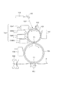
図3において、10は電磁誘導発熱層(導電体層、磁性体層、抵抗体層)を有する、電磁誘導発熱性の回転体としての円筒状の定着フィルム(定着ベルト)である。16は横断面略半円弧状樋型のフィルムガイド(ベルトガイド)部材であり、円筒状の定着フィルム10はこのフィルムガイド部材16の外側にルーズに外嵌させてある。15はフィルムガイド部材16の内側に配設した磁場発生手段であり、励磁コイル18とE型の磁性コア(芯材)17とからなる。30は弾性加圧ローラであり、定着フィルム10を挟ませてフィルムガイド部材16の下面と所定の圧接力をもって所定幅の定着ニップ部Nを形成させて相互圧接させてある。上記磁場発生手段15の磁性コア17は、定着ニップ部Nに対応位置させて配設してある。
【0016】
加圧ローラ30は、駆動手段Mにより矢示の反時計方向に回転駆動される。この加圧ローラ30の回転駆動による該加圧ローラ30と定着フィルム10の外面との摩擦力で定着フィルム10に回転力が作用して、該定着フィルム10がその内面が定着ニップ部Nにおいてフィルムガイド部材16の下面に密着して摺動しながら、矢示の時計方向に加圧ローラ30の回転周速度に略対応した周速度をもってフィルムガイド部材16の外回りを回転状態になる(加圧ローラ駆動方式)。
【0017】
フィルムガイド部材16は、定着ニップ部Nへの加圧、磁場発生手段15としての励磁コイル18と磁性コア17の支持、定着フィルム10の支持、該定着フィルム10の回転時の搬送安定性を図る役目をする。このフィルムガイド部材16は、磁束の通過を妨げない絶縁性の部材であり、高い荷重に耐えられる材料が用いられる。
【0018】
励磁コイル18は、不図示の励磁回路から供給される交番電流によって交番磁束を発生する。交番磁束は、定着ニップ部Nの位置に対応しているE型の磁性コア17により定着ニップ部Nに集中的に分布し、その交番磁束は、定着ニップ部Nにおいて定着フィルム10の電磁誘導発熱層に渦電流を発生させる。この渦電流は、電磁誘導発熱層の固有抵抗によって電磁誘導発熱層にジュール熱を発生させる。
【0019】
この定着フィルム10の電磁誘導発熱は、交番磁束を集中的に分布させた定着ニップ部Nにおいて集中的に生じて定着ニップ部Nが高効率に加熱される。定着ニップ部Nの温度は、不図示の温度検知手段を含む温調系により励磁コイル18に対する電流供給が制御されることで所定の温度が維持されるように温調される。
【0020】
而して、加圧ローラ30が回転駆動され、それに伴って円筒状の定着フィルム10がフィルムガイド部材16の外回りを回転し、励磁回路から励磁コイル18への給電により上記のように定着フィルム10の電磁誘導発熱がなされて定着ニップ部Nが所定の温度に立ち上がって温調された状態において、不図示の画像形成手段から搬送された未定着トナー画像tが形成された被記録材Pが定着ニップ部Nの定着フィルム10と加圧ローラ30との間に画像面が上向き、即ち、定着フィルム面に対向して導入され、定着ニップ部Nにおいて画像面が定着フィルム10の外面に密着して定着フィルム10と一緒に定着ニップ部Nを挟持搬送されていく。
【0021】
この定着ニップ部Nを定着フィルム10と一緒に被記録材Pが挟持搬送されていく過程において、定着フィルム10の電磁誘導発熱で加熱されて被記録材P上の未定着トナー画像tが加熱定着される。被記録材Pは、定着ニップ部Nを通過すると、回転中の定着フィルム10の外面から分離して排出搬送されていく。
【0022】
このような構成における電磁誘導加熱電源に用いるインバータ回路としては、大別して電流共振型電源方式と電圧共振方式がある。共振方式を用いるのは、比較的大きな電力を取扱う時、変換用のスイッチング素子の損失を低減させるために、スイッチング時に生じる電圧または電流の振動状態を積極的に生成し、スイッチング素子に最も電圧または電流及び両者の値が低い時を見計らってスイッチングを行う方式で、ソフトスイッチングと称しており、大電力を取扱う上で最も有効な方式であり、様々な方式が提案されている。
【0023】
従来例として図16に電圧共振方式インバータ回路を示す。図16において、202はスイッチング素子、203は共振コイル(励磁コイル)、205は共振コンデンサである。周知の電圧共振インバータの動作は、スイッチング素子202がオンして電力を共振コイル203に蓄積した後スイッチング素子202をオフすると、共振コイル203と共振コンデンサ205の定数で定まる周期で電圧が共振の弧を描きながら振動を開始する。この時の様子を図17に示す。
【0024】
図18に出力電力を絞り込むためにゲートスイッチング信号のオン幅を縮小して電力変換動作を行った時の動作波形を示す。出力電力を絞り込んだ時のスイッチング素子202の電圧波形は、共振コイル203の端子接続された電源電圧(破線で示すレベル)を基準として共振減衰するサイン波を描く。電圧の振動振幅は、共振コイル(励磁コイル)203に蓄積した励磁電力、即ち、スイッチング素子202のオン幅に依存するもので、省電力時には振動振幅が低く、電源電圧レベルから充分に電圧が低下せず、ゼロクロスが得られない。
【0025】
即ち、スイッチング素子202は、電源ラインを介して共振コンデンサ205の極めて低インピーダンスの負荷をスイッチングすることとなり、スイッチングオン時に過大な電流が流れてしまう。この過大な電流によりスイッチング素子202を破壊させない範囲は、電圧共振電源では最大出力の1/3程度までしか絞り込むことができず、設計を困難にしている。
【0026】
【発明が解決しようとする課題】
しかしながら、上述した従来技術においては下記のような問題があった。即ち、画像形成装置に搭載される定着加熱装置で用いる電力制御領域の要求幅は、1100W〜150Wのものが主流である。また、本件で提案する誘導加熱電源の方式としては電流共振方式と電圧共振方式に大別される中で、簡素な構成で実現できる電圧共振方式が主流である。
【0027】
ところが、従来の電圧共振方式での電力制御は、最大出力時の1/3程度、即ち上記例では350W迄しか電力を絞り込むことができず、それ以上に電力を絞り込もうとした際には電圧共振状態を逸脱してスイッチング素子に大電流が流れ破損させてしまうといった欠点があった。
【0028】
画像形成装置においてこのような電源で定着制御を行うと、連続プリント時の温度飽和状態において350Wでは電力過剰となり回路が間欠動作してしまう。このような間欠動作制御では温度の不安定動作を来すと共に、電圧共振回路は共振コンデンサとコイルの並列回路が付加されているため、起動時には過大な電流が流れスイッチング素子にストレスを与えてしまうという課題があった。
【0029】
本発明は、上述した点に鑑みなされたものであり、従来の電圧共振電源の弱点であった狭い出力制御幅を広げると共に、スイッチング制御素子として大電流を許容し低コストであるが、FETに比較して損失が大きいIGBT(Insulated Gate Bipolar Transistor)を採用した場合に特に好適な、ゲート信号波形を最適化し制御時におけるスイッチング損失を極小とすることが可能な画像形成装置用電源装置及びそれを用いた画像形成装置並びに定着装置を提供することを目的とする。
【0030】
【課題を解決するための手段】
上記目的を達成するために、本発明による画像形成装置用電源装置は、
電源に接続された第1のIGBT(Insulated Gate Bipolar Transistor)と、該第1のIGBTに直列接続された第1の蓄電手段と、該第1の蓄電手段に直列接続された第2のIGBTと、前記第1の蓄電手段及び前記第2のIGBTの接続点と前記電源との間に接続された磁場発生手段と、前記第2のIGBTに並列接続された第2の蓄電手段と、前記第1のIGBTに並列接続された第1の整流手段と、前記第2のIGBTに並列接続された第2の整流手段とを有する電圧共振コンバータ手段と、絶縁型トランスの出力端子を介して伝達される伝達電圧を波形整形して、前記第1及び第2のIGBTのゲートを駆動する駆動電圧として出力する絶縁型駆動回路手段であって、予め設定された閾値電圧を生成する閾値電圧生成手段と、前記伝達電圧の電圧下降時に、前記伝達電圧が前記閾値電圧を下回ったことを検出する検出手段と、前記検出に応答して前記絶縁型トランスの出力端子間を短絡する第1のスイッチング手段を有することを特徴とする絶縁型駆動回路手段とを有することを特徴とする。
【0031】
また、上記目的は、励磁コイルに電力を供給する電源装置であって、電力スイッチング半導体を含む電圧共振コンバータ回路と、電力スイッチング半導体を駆動する駆動回路とを有し、駆動回路が、トランスと、トランスの一次巻線に接続された第1のスイッチング回路と、電力スイッチング半導体を駆動するために、第1のスイッチング回路を駆動することによりトランスの二次巻線から出力される電圧を整流した信号を電力スイッチング半導体に出力する整流素子と、閾値電圧を設定するための閾値設定回路と、第1のスイッチング回路の駆動を停止した際に、トランスの二次巻線から出力される電圧が閾値電圧を下回ると、トランスの二次巻線の出力端子間を短絡して、電力スイッチング半導体の駆動を停止するための第2のスイッチング回路と、を有することを特徴とする電源装置によっても達成される。
また、上記目的は、記録媒体に画像を形成する画像形成手段と、電磁誘導発熱部材と、電磁誘導発熱部材に渦電流を誘導する磁束を生成する励磁コイルを有し、記録媒体に画像を定着するための定着手段と、電力スイッチング半導体を有する電圧共振コンバータ回路と、前記電力スイッチング半導体を駆動する駆動回路を有する電源装置と、を備える画像形成装置であって、駆動回路が、トランスと、トランスの一次巻線に接続された第1のスイッチング回路と、電力スイッチング半導体を駆動するために、第1のスイッチング回路を駆動することによりトランスの二次巻線から出力される電圧を整流した信号を電力スイッチング半導体に出力する整流素子と、閾値電圧を設定するための閾値設定回路と、第1のスイッチング回路の駆動を停止した際に、トランスの二次巻線から出力される電圧が閾値電圧を下回ると、トランスの二次巻線の出力端子間を短絡して、電力スイッチング半導体の駆動を停止するための第2のスイッチング回路と、を有することを特徴とする画像形成装置によっても達成される。
【0032】
【作用】
電圧共振コンバータは、電源に接続されたIGBT201と、IGBT201に直列接続された第1の共振コンデンサ204と、第1の共振コンデンサ204に直列接続されたIGBT202と、第1の共振コンデンサ204及びIGBT202の接続点と電源との間に接続された励磁コイル18と、IGBT202に並列接続された第2の共振コンデンサ205と、IGBT201、IGBT202にそれぞれ並列接続された回生ダイオード206、207とを有し、各々のIGBT201及び202のゲート制御信号は絶縁型駆動トランスの伝達電圧3からスイッチングタイミング信号を波形整形して生成し、確実なスイッチング動作を保証する構成としたものである。
【0033】
【発明の実施の形態】
以下、図面を参照して本発明をその好適な実施形態に基づいて説明する。
(第1の実施形態)
先ず、本発明の電源装置が適用される画像形成装置の一例について説明する。図2は本発明の第1の実施の形態に係る画像形成装置の構成を示す構成図である。本例では、画像形成装置として例えば電子写真カラープリンタの場合を例に説明するがこれに限定されるものではない。画像形成装置は、定着装置(像加熱装置)100、感光体ドラム(像担持体)101、帯電装置102、4色カラー現像装置104、中間転写体ドラム105、転写ローラ106、クリーナ107、ミラー109、レーザ光学箱(レーザスキャナ)110を備えている。
【0034】
上記各部の構成を動作と共に詳述すると、感光体ドラム(像担持体)101は、有機感光体やアモルファスシリコン感光体で構成されており、矢示の反時計方向に所定のプロセススピード(周速度)で回転駆動される。感光体ドラム101は、その回転過程で帯電ローラ等の帯電装置102で所定の極性・電位の一様な帯電処理を受ける。次いで、感光体ドラム101は、その帯電処理面にレーザ光学箱110から出力されるレーザ光103による目的の画像情報の走査露光処理を受ける。レーザ光学箱110は、不図示の画像読取装置等の画像信号発生装置からの目的画像情報の時系列電気デジタル画素信号に対応して変調(オン/オフ)したレーザ光103を出力して、回転中の感光体ドラム101面に走査露光した目的画像情報に対応した静電潜像を形成する。ミラー109は、レーザ光学箱110からの出力レーザ光を感光体ドラム101の露光位置に偏向させる。
【0035】
フルカラー画像の場合は、目的のフルカラー画像の第1の色分解成分画像、例えばイエロー成分画像についての走査露光・潜像形成がなされ、その潜像が4色カラー現像装置104のうちのイエロー現像器104Yの作動でイエロートナー画像として現像される。そのイエロートナー画像は、感光体ドラム101と中間転写体ドラム105との接触部(或いは近傍部)である1次転写部T1において中間転写体ドラム105の面に転写される。中間転写体ドラム105面に対するトナー画像転写後の回転感光体ドラム101面は、クリーナ107により転写残りトナー等の付着残留物の除去を受けて清掃される。
【0036】
上記のような帯電・走査露光・現像・一次転写・清掃のプロセスサイクルが、目的のフルカラー画像の第2の色分解成分画像(例えばマゼンタ成分画像、マゼンタ現像器104が作動)、第3の色分解成分画像(例えばシアン成分画像、シアン現像器104Cが作動)、第4の色分解成分画像(例えば黒成分画像、黒現像器104BKが作動)の各色分解成分画像について順次実行され、中間転写体ドラム105面にイエロートナー画像・マゼンタトナー画像・シアントナー画像・黒トナー画像の都合4色のトナー画像が順次重ねて転写されて、目的のフルカラー画像に対応したカラートナー画像が合成形成される。
【0037】
中間転写体ドラム105は、金属ドラム上に中抵抗の弾性層と高抵抗の表層を有するもので、感光体ドラム101に接触して或いは近接して感光体ドラム101と略同じ周速度で矢示の時計方向に回転駆動され、中間転写体ドラム105の金属ドラムにバイアス電位を与えて感光体ドラム101との電位差で、感光体ドラム101側のトナー画像を中間転写体ドラム105面側に転写させる。
【0038】
上記の回転中間転写体ドラム105面に合成形成されたカラートナー画像は、回転中間転写体ドラム105と転写ローラ106との接触ニップ部である二次転写部T2において、該二次転写部T2に不図示の給紙部から所定のタイミングで送り込まれた被記録材Pの面に転写されていく。転写ローラ106は、被記録材Pの背面からトナーと逆極性の電荷を供給することで、中間転写体ドラム105面側から被記録材P側へ合成カラートナー画像を順次に一括転写する。二次転写部T2を通過した被記録材Pは、中間転写体ドラム105の面から分離されて定着装置(像加熱装置)100へ導入され、未定着トナー画像の加熱定着処理を受けてカラー画像形成物として機外の不図示の排紙トレイに排出される。定着装置(像加熱装置)100については下記の(2)項で詳述する。
【0039】
被記録材Pに対するカラートナー画像転写後の回転中間転写体ドラム105は、上記のようにクリーナ107により転写残りトナー・紙粉等の付着残留物の除去を受けて清掃される。このクリーナ107は、常時は中間転写体ドラム105に非接触状態に保持されており、中間転写体ドラム105から被記録材Pに対するカラートナー画像の二次転写実行過程において中間転写体ドラム105に接触状態に保持される。また、転写ローラ106も、常時は中間転写体ドラム105に非接触状態に保持されており、中間転写体ドラム105から被記録材Pに対するカラートナー画像の二次転写実行過程において中間転写体ドラム105に被記録材Pを介して接触状態に保持される。
【0040】
本例の画像形成装置は、白黒画像などモノカラー画像のプリントモードも実行できる。また、両面画像プリントモード或いは多重画像プリントモードも実行できる。両面プリントモードの場合は、定着装置(像加熱装置)100を出た1面目画像プリント済みの被記録材Pは、不図示の再循環搬送機構を介して表裏反転されて再び二次転写部T2へ送り込まれて2面に対するトナー画像転写を受け、再度、定着装置(像加熱装置)100に導入されて2面に対するトナー画像の定着処理を受けることで両面画像プリントが出力される。
【0041】
多重画像プリントモードの場合は、定着装置(像加熱装置)100を出た1回面画像プリント済みの被記録材Pは、不図示の再循環搬送機構を介して表裏反転されずに再び二次転写部T2へ送り込まれて1回目画像プリント済みの面に2回目のトナー画像転写を受け、再度、定着装置(像加熱装置)100に導入されて2回目のトナー画像の定着処理を受けることで多重画像プリントが出力される。
【0042】
(2)定着装置(像加熱装置)100
次に、上述した画像形成装置の定着装置(像加熱装置)100について説明する。本例の定着装置(像加熱装置)100は、円筒状の電磁誘導発熱ベルトを用いた加圧ローラ駆動方式、電磁誘導加熱方式の装置である。図3は本発明の第1の実施の形態に係る画像形成装置における定着装置の要部の横断側面構成を示す構成図、図4は定着装置の要部の正面構成を示す構成図、図5は定着装置の要部の縦断正面構成を示す構成図である。
【0043】
定着装置(像加熱装置)100各部の構成を詳述すると、磁場発生手段は、磁性コア17a・17b・17c及び励磁コイル18からなる。磁性コア17a・17b・17cは、高透磁率の部材であり、フェライトやパーマロイ等といったトランスのコアに用いられる材料がよく、より好ましくは100KHz以上でも損失の少ないフェライトを用いるのがよい。励磁コイル18には、給電部18a・18bに励磁回路27(図6参照)を接続してある。この励磁回路27は、20KHzから500KHzの高周波をスイッチング電源で発生できるようになっている。励磁コイル18は、励磁回路27から供給される交番電流(高周波電流)によって交番磁束を発生する。
【0044】
16a、16bは横断面略半円弧状樋型のベルトガイド部材であり、開口側を互いに向かい合わせて略円柱体を構成し、外側に円筒状の電磁誘導性発熱ベルトである定着ベルト10をルーズに外嵌させてある。ベルトガイド部材16aは、磁場発生手段としての磁性コア17a・17b・17cと励磁コイル18を内側に保持している。また、ベルトガイド部材16aには、図5に示すように紙面垂直方向長手の良熱伝導部材40がニップ部Nの加圧ローラ30との対向面側で、定着ベルト10の内側に配設してある。本例においては、良熱伝導部材40にアルミニウムを用いている。良熱伝導部材40は熱伝導率が、
k=240[W・m−1・K−1]
であり、厚さ1[mm]である。
【0045】
また、良熱伝導部材40は、磁場発生手段である励磁コイル18と磁性コア17a・17b・17cから発生する磁場の影響を受けないように、この磁場の外に配設してある。具体的には、良熱伝導部材40を励磁コイル18に対して磁性コア17cを隔てた位置に配設し、励磁コイル18による磁路の外側に位置させて良熱伝導部材40に影響を与えないようにしている。
【0046】
22はベルトガイド部材16bの内面平面部に当接させて配設した横長の加圧用剛性ステイである。19は磁性コア17a・17b・17c及び励磁コイル18と加圧用剛性ステイ22の間を絶縁するための絶縁部材である。フランジ部材23a・23bは、ベルトガイド部材16a、16bのアセンブリの左右両端部に外嵌し、前記左右位置を固定しつつ回転自在に取り付け、定着ベルト10の回転時に該定着ベルト10の端部を受けて該定着ベルト10のベルトガイド部材長手に沿う、寄り移動を規制する役目をする。
【0047】
加圧部材としての加圧ローラ30は、芯金30aと、芯金30a周りに同心一体にローラ状に形成被覆させた、シリコンゴム・フッ素・フッ素樹脂などの耐熱性・弾性材層30bとで構成されており、芯金30aの両端部を装置の不図示のシャーシ側板金間に回転自在に軸受け保持させて配設してある。加圧用剛性ステイ22の両端部と装置シャーシ側のバネ受け部材29a・29bとの間にそれぞれ加圧バネ25a・25bを縮設することで、加圧用剛性ステイ22に押し下げ力を作用させている。これにより、ベルトガイド部材16aの下面と加圧ローラ30の上面とが定着ベルト10を挟んで圧接して所定幅の定着ニップ部Nが形成される。
【0048】
加圧ローラ30は、駆動手段Mにより矢示の反時計方向に回転駆動される。この加圧ローラ30の回転駆動による該加圧ローラ30と定着ベルト10の外面との摩擦力で定着ベルト10に回転力が作用し、定着ベルト10がその内面が定着ニップ部Nにおいて良熱伝導部材40の下面に密着して摺動しながら、矢示の時計方向に加圧ローラ30の回転周速度に略対応した周速度をもってベルトガイド部材16a、16bの外回りを回転状態になる。
【0049】
この場合、定着ニップ部Nにおける良熱伝導部材40の下面と定着ベルト10の内面との相互摺動摩擦力を低減化させるために、定着ニップ部Nの良熱伝導部材40の下面と定着ベルト10の内面との間に耐熱性グリスなどの潤滑剤を介在させる。或いは、良熱伝導部材40の下面を潤滑部材で被覆することもできる。これは、良熱伝導部材40としてアルミニウムを用いた場合のように表面滑り性が材質的によくない或いは仕上げ加工を簡素化した場合に、摺動する定着ベルト10に傷をつけて定着ベルト10の耐久性が悪化してしまうことを防ぐものである。
【0050】
良熱伝導部材40は、長手方向の温度分布を均一にする効果があり、例えば、小サイズ紙を通紙した場合、定着ベルト10での非通紙部の熱量が良熱伝導部材40へ伝熱し、良熱伝導部材40における長手方向の熱伝導により、非通紙部の熱量が小サイズ紙通紙部へ伝熱される。これにより、小サイズ紙通紙時の消費電力を低減させる効果も得られる。
【0051】
また、図6に示すように、ベルトガイド部材16aの周面に、その長手に沿い所定の間隔を置いて凸リブ部16eを形成具備させ、ベルトガイド部材16aの周面と定着ベルト10の内面との接触摺動抵抗を低減させて抵抗ベルト10の回転負荷を少なくしている。
【0052】
図7は交番磁束の発生の様子を模式的に表したものである。磁束Cは発生した交番磁束の一部を表す。磁性コア17a・17b・17cに導かれた交番磁束Cは、磁性コア17aと磁性コア17bとの間、そして磁性コア17aと磁性コア17cとの間において、定着ベルト10の電磁誘導発熱層1に渦電流を発生させる。この渦電流は、電磁誘導発熱層1の固有抵抗によって電磁誘導発熱層1にジュール熱(渦電流損)を発生させる。
【0053】
ここでの発熱量Qは、電磁誘導発熱層1を通る磁束の密度によって決まり図7のグラフのような分布を示す。図7のグラフは、縦軸が磁性コア17aの中心を0とした角度θで表した定着ベルト10における円周方向の位置を示し、横軸が定着ベルト10の電磁誘導発熱層1での発熱量Qを示す。ここで、発熱域Hは、最大発熱量をQとした場合、発熱量がQ/e以上の領域と定義する。これは、定着に必要な発熱量が得られる量である。
【0054】
この定着ニップ部Nの温度は、不図示の温度検知手段を含む温調系により励磁コイル18に対する電流供給が制御されることで所定の温度が維持されるように温調される。上記図3の26は定着ベルト10の温度を検知するサーミスタなどの温度センサであり、本例においては温度センサ26で測定した定着ベルト10の温度情報を基に定着ニップ部Nの温度を制御するようにしている。
【0055】
而して、定着ベルト10が回転し、励磁回路27から励磁コイル18への給電により上記のように定着ベルト10の電磁誘導発熱がなされて定着ニップ部Nが所定の温度に立ち上がって温調された状態において、画像形成手段部から搬送された未定着トナー画像tが形成された被記録材Pが定着ニップ部Nの定着ベルト10と加圧ローラ30との間に画像面が上向き、即ち定着ベルト面に対向して導入され、定着ニップ部Nにおいて画像面が定着ベルト10の外面に密着して定着ベルト10と一緒に定着ニップ部Nを挟持搬送されていく。
【0056】
この定着ニップ部Nを定着ベルト10と一緒に被記録材Pが挟持搬送されていく過程において、定着ベルト10の電磁誘導発熱で加熱されて被記録材P上の未定着トナー画像tが加熱定着される。被記録材Pは、定着ニップ部Nを通過すると回転定着ベルト10の外面から分離して排出搬送されていく。被記録材P上の加熱定着トナー画像は、定着ニップ部通過後、冷却して永久固着像となる。
【0057】
本例においては、上記図3に示すように、定着ベルト10のこの発熱域H(図7参照)の対向位置に暴走時の励磁コイル18への給電を遮断するため、温度検知素子であるサーモスイッチ150を配設している。
【0058】
図8は本例で使用した安全回路の回路図である。温度検知素子であるサーモスイッチ150は、+24VDC電源とリレースイッチ151と直列に接続されており、サーモスイッチ150が切れるとリレースイッチ151への給電が遮断されリレースイッチ151が動作し、励磁回路27への給電が遮断されることにより励磁コイル18への給電を遮断する構成をとっている。サーモスイッチ150はOFF動作温度を220度Cに設定した。また、サーモスイッチ150は、定着ベルト(フィルム)10の発熱域Hに対向して定着ベルト10の外面に非接触に配設した。サーモスイッチ150と定着ベルト10との間の距離は略2mmとした。これにより、定着ベルト10にサーモスイッチ150の接触による傷が付くことがなく、耐久による定着画像の劣化を防止することができる。
【0059】
本例によれば、装置故障による定着装置暴走時、図3のような定着ニップ部Nで発熱する構成とは違い、定着ニップ部Nに紙が挟まった状態で定着装置(定着器)が停止し、励磁コイル18に給電が続けられ定着ベルト10が発熱し続けた場合でも、紙が挟まっている定着ニップ部Nでは発熱していないために紙が直接加熱されることがない。また、発熱量が多い発熱域Hにはサーモスイッチ150が配設してあるため、サーモスイッチ150が220度Cを感知してサーモスイッチ150が切れた時点で、リレースイッチ151により励磁コイル18への給電が遮断される。また、本例によれば、紙の発火温度は約400度C近辺であるため紙が発火することなく、定着ベルト10の発熱を停止することができる。
【0060】
尚、温度検知素子としてサーモスイッチの他に温度ヒューズを用いることもできる。また、本例ではトナーtに低軟化物質を含有させたトナーを使用したため、定着装置にオフセット防止のためのオイル塗布機構を設けていないが、低軟化物質を含有させていないトナーを使用した場合にはオイル塗布機構を設けてもよい。また、低軟化物質を含有させたトナーを使用した場合にもオイル塗布や冷却分離を行ってもよい。
【0061】
次に、上述した定着装置100の励磁コイル18及び定着ベルト10について更に詳細に説明する。
(A)励磁コイル18
励磁コイル18は、コイル(線輪)を構成させる導線(電線)として一本ずつがそれぞれ絶縁被覆された銅製の細線を複数本束ねたもの(束線)を用い、これを複数回巻いて励磁コイルを形成している。本例では10ターン巻いて励磁コイル18を形成している。絶縁被覆は定着ベルト10の発熱による熱伝導を考慮して耐熱性を有する被覆を用いるのがよい。例えば、アミドイミドやポリイミドなどの被覆を用いるとよい。励磁コイル18は外部から圧力を加えて密集度を向上させてもよい。
【0062】
励磁コイル18の形状は、上記図3のように発熱層の曲面に沿うようにしている。本例では定着ベルト10の発熱層と励磁コイル18との間の距離は略2mmになるように設定した。励磁コイル保持部材19の材質としては絶縁性に優れ耐熱性のよいものがよい。例えば、フェノール樹脂、フッ素樹脂、ポリイミド樹脂、ポリアミド樹脂、ポリアミドイミド樹脂、PEEK樹脂、PES樹脂、PPS樹脂、PFA樹脂、PTFE樹脂、FEP樹脂、LCP樹脂などを選択するとよい。
【0063】
磁性コア17a・17b・17c及び励磁コイル18と定着ベルト10の発熱層の間の距離はできる限り近付けた方が磁束の吸収効率が高いのであるが、この距離が5mmを超えるとこの効率が著しく低下するため5mm以内にするのがよい。また、5mm以内であれば定着ベルト10の発熱層と励磁コイル18の距離が一定である必要はない。励磁コイル18の励磁コイル保持部材19からの引出線、即ち18a・18b(図6)については、励磁コイル保持部材19から外の部分について束線の外側に絶縁被覆を施している。
【0064】
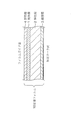
(B)定着ベルト(定着フィルム)10
図9は本例における定着ベルト(定着フィルム)10の層構成を示す説明図である。本例の定着ベルト(定着フィルム)10は、電電磁誘導発熱性の定着ベルト10の基層となる金属ベルト等で構成された発熱層1と、その外面に積層した弾性層2と、その外面に積層した離型層3との複合構造となっている。発熱層1と弾性層2との間の接着、弾性層2と離型層3との間の接着のため、各層間にプライマー層(不図示)を設けてもよい。略円筒形状である定着ベルト10において発熱層1が内面側であり、離型層3が外面側である。上述したように、発熱層1に交番磁束が作用することで発熱層1に渦電流が発生して発熱層1が発熱する。その熱が弾性層2・離型層3を介して定着ベルト10を加熱し、定着ニップ部Nに通紙される被加熱材としての被記録材Pを加熱してトナー画像の加熱定着がなされる。
【0065】
(a)発熱層1
発熱層1は、ニッケル、鉄、強磁性SUS、ニッケルーコバルト合金といった強磁性体の金属を用いるとよい。非磁性の金属でもよいが、より好ましくは磁束の吸収のよいニッケル、鉄、磁性ステンレス、コバルトーニッケル合金等の金属がよい。その厚みは次の式で表される表皮深さより厚く且つ200μm以下にすることが好ましい。表皮深さσ[m]は、励磁回路27の周波数f[Hz]と透磁率μと固有抵抗ρ[Ωm]で、
σ=503×(ρ/fμ)1/2
と表される。
【0066】
これは、電磁誘導で使われる電磁波の吸収の深さを示しており、これより深いところでは電磁波の強度は1/e以下になっており、逆に言うと殆どのエネルギはこの深さまでで吸収されている(図10参照)。図10は電磁波強度と発熱層深さとの関係を示す図である。発熱層1の厚さは好ましくは1〜100μmがよい。発熱層1の厚みが1μmよりも小さいと殆どの電磁エネルギが吸収しきれないため効率が悪くなる。また、発熱層1が100μmを超えると剛性が高くなりすぎ、また屈曲性が悪くなり回転体として使用するには現実的ではない。従って、発熱層1の厚みは1〜100μmが好ましい。
【0067】
(b)弾性層2
弾性層2は、シリコンゴム、フッ素ゴム、フルオロシリコンゴム等で耐熱性がよく熱伝導率がよい材質である。弾性層2の深さは10〜500μmが好ましい。この弾性層2は定着画像品質を保証するために必要な厚さである。カラー画像を印刷する場合、特に写真画像などでは被記録材P上で大きな面積に渡ってベタ画像が形成される。この場合、被記録材の凹凸或いはトナー層の凹凸に加熱面(離型層3)が追従できないと加熱ムラが発生し、伝熱量が多い部分と少ない部分で画像に光沢ムラが発生する。
【0068】
伝熱量が多い部分は光沢度が高く、伝熱量が少ない部分では光沢度が低い。弾性層2の厚さとしては、10μm以下では被記録材或いはトナー層の凹凸に追従しきれず画像光沢ムラが発生してしまう。また、弾性層2が1000μm以上の場合には弾性層2の熱抵抗が大きくなりクイックスタートを実現するのが難しくなる。より好ましくは弾性層2の厚みは50〜500μmがよい。
【0069】
弾性層2の硬度は、硬度が高すぎると被記録材或いはトナー層の凹凸に追従しきれず画像光沢ムラが発生してしまう。そこで、弾性層2の硬度としては60度(JIS−A)以下、より好ましくは45度(JIS−A)以下がよい。弾性層2の熱伝導率λに関しては、
6×10⁻⁴≦λ≦2×10⁻³[cal/cm・sec・deg.]
がよい。
【0070】
熱伝導率λが、
λ<6×10⁻⁴[cal/cm・sec・deg.]
の場合には、熱抵抗が大きく、定着ベルト10の表層(離型層3)における温度上昇が遅くなる。
【0071】
熱伝導率λが、
λ>2×10⁻³[cal/cm・sec・deg.]
の場合には、硬度が高くなりすぎたり、圧縮永久歪みが悪化する。
【0072】
よって、熱伝導率λは、
6×10⁻⁴≦λ≦2×10⁻³[cal/cm・sec・deg.]
がよい。より好ましくは、
8×10⁻⁴≦λ≦1.5×10⁻³[cal/cm・sec・deg.]
がよい。
【0073】
(c)離型層3
離型層3は、フッ素樹脂、シリコン樹脂、フルオロシリコンゴム、フッ素ゴム、シリコンゴム、PFA、PTFE、FEP等の離型性且つ耐熱性のよい材料を選択することができる。離型層3の厚さは1〜100μmが好ましい。離型層3の厚さが1μmよりも小さいと塗膜の塗ムラで離型性の悪い部分ができたり、耐久性が不足するといった問題が発生する。また、離型層3が100μmを超えると熱伝導が悪化するという問題が発生し、特に樹脂系の離型層の場合は硬度が高くなりすぎ、弾性層2の効果がなくなってしまう。
【0074】
また、図11に示すように、定着ベルト(定着フィルム)10の構成において、発熱層1のベルトガイド面側(発熱層1の弾性層2とは反対側面)に断熱層4を設けてもよい。断熱層4としては、フッ素樹脂、ポリイミド樹脂、ポリアミド樹脂、ポリアミドイミド樹脂、PEEK樹脂、PES樹脂、PPS樹脂、PFA樹脂、PTFE樹脂、FEP樹脂などの断熱樹脂がよい。
【0075】
また、断熱層4の厚さとしては10〜1000μmが好ましい。断熱層4の厚さが10μmよりも小さい場合には断熱効果が得られず、また、耐久性も不足する。一方、1000μmを超えると磁性コア17a・17b・17c及び励磁コイル18から発熱層1への距離が大きくなり、磁束が十分に発熱層1に吸収されなくなる。断熱層4は、発熱層1に発生した熱が定着ベルト10の内側に向かわないように断熱できるので、断熱層4がない場合と比較して被記録材P側への熱供給効率が良くなる。よって、消費電力を抑えることができる。
【0076】
図12は本発明の第1の実施の形態に係る画像形成装置における、後述の図1に示す出力コンバータを含む誘導加熱制御部の全体構成を示すブロック図である。画像形成装置の誘導加熱制御部は、電圧制御回路409、定着器ユニット部(Fuser)411、フィードバック制御回路413、ドライバ回路414を備えている。更に、上記電圧制御回路409は、過電流ブレーカ402、リレー403、整流回路(RECT)404、絶縁型ゲート駆動回路部405、406、電圧共振コンバータ部407、カレントトランス408を備えている。図中401は電源ライン入力端子、412は定着器の加熱オン/オフ信号を示す。
【0077】
上記要部の構成を動作と共に詳述すると、過電流ブレーカ402は、過電流を保護する。整流回路404は、交流入力から両波整流を行うブリッジ整流回路と高周波フィルタを行うコンデンサで構成されている。電圧共振コンバータ部407は、電流のスイッチングを行う。カレントトランス408は、電圧共振コンバータ部407でスイッチングされたスイッチング電流を検出するトランスであり、定着器(定着装置)の励磁コイル18と接続される。
【0078】
定着器ユニット部411は、電気部品構成としては上述した励磁コイル18と、温度検出サーミスタ(温度センサ)26と、過昇温を検出するサーモスイッチ150を有している。定着器の加熱オン/オフ信号412は、不図示の画像形成装置(プリンタ)シーケンスコントローラから送られてくる。フィードバック制御回路413は、定着器のサーミスタ温度検出値に基づき、目標温度と比較しながら制御両をコントロールする。ドライバ回路414は、フィードバック制御回路413からのフィードバック制御信号を受けて、本コンバータの制御形態に相応しい制御を行う。
【0079】
電源ライン入力端子401から交流入力電源を受け、過電流ブレーカ402及びリレー403を介して整流回路404に交流電源が印加されると、該整流回路404の両波整流ダイオードにより脈動化直流電源を生成する。その後、電圧共振コンバータ部407でスイッチング素子を交互スイッチングを行うように絶縁型ゲート駆動回路部405、406をドライブすることにより、励磁コイル18に高周波電圧が印加される。励磁コイル18に流れる電流を制御することにより、定着ベルト(定着フィルム)10に流れる渦電流を可変し、発熱電力を制御するものである。
【0080】
更に、図12に基づき説明すると、電源入力端子401から交流電力を受けると、交流電力は、過電流を保護する過電流ブレーカ402及びリレー403の接点を介して整流回路404に入る。ここで、リレー403の励磁巻線は定着器のベルト(フィルム)温度を検出し、ベルト(フィルム)温度が規定の温度を超え異常昇温したとき遮断するサーモスイッチ150の接点を介して励磁するように構成されている。仮にトラブルが生じ本定着器が異常昇温をした時、リレー403を遮断して励磁回路の電源を切り、熱暴走から定着器の安全を確保している。整流回路404では、不図示の整流ブリッジ回路により交流電源から直流化リップ波を生成し、LCフィルタを介して電圧共振コンバータ部407の電源として供給する。電圧共振コンバータ部407での動作については後述の図1で説明する。
【0081】
カレントトランス(電流検出トランス)408、絶縁型ゲート駆動回路部405、406は、ライブ電圧回路と二次電圧回路をトランスの絶縁処理によって二重絶縁を確保するよう構成されている。定着温度は温度センサ(サーミスタ)26で検出され、定着器の通紙状態や紙質、定着温度で異なる最適な制御係数を与えられた制御信号は、ドライバ回路414により本電源の電圧共振制御に相応しいオン幅制御信号で半導体スイッチング素子のゲート制御を行う。
【0082】
電圧共振方式コンバータでは、目標温度に対してその過不足をスイッチングオン幅で制御する。その構成及び動作について図1及び図13を用いて詳細に説明する。
図1は本発明の第1の実施の形態に係る、電圧共振方式電源装置の構成例を示す回路図である。本発明の第1の実施の形態に係る電源装置は、スイッチングIGBT201(第1のスイッチング手段)、主スイッチングIGBT202(第2のスイッチング手段)、第1の共振コンデンサ204(第1の蓄電手段)、第2の共振コンデンサ205(第2の蓄電手段)、回生ダイオード206(第1の整流手段)、回生ダイオード207(第2の整流手段)を備える電圧共振コンバータ部407と、2つのIGBT201及び202をそれぞれ駆動する2つのゲート駆動回路部405、406(後述)とから構成される。
【0083】
まず、電圧共振コンバータ部407について説明する。電源に接続されたスイッチングIGBT201には、第1の共振コンデンサ204が直列に接続されており、第1の共振コンデンサ204には、主スイッチングIGBT202が直列に接続されている。また、第1の共振コンデンサ204、主スイッチングIGBT202の接続点と電源との間には、磁気誘導加熱用の励磁コイル18が接続されており、主スイッチングIGBT202には、第2の共振コンデンサ205が並列に接続されている。また、スイッチングIGBT201、主スイッチングIGBT202には、それぞれ回生ダイオード(整流素子)206、207が並列に接続されている。
【0084】
また、図13は図1の回路構成における動作波形を示す説明図である。208はスイッチングIGBT201のゲート電圧波形、209は主スイッチングIGBT202のゲート電圧波形、210は主スイッチングIGBT202の電流波形、211は主スイッチングIGBT202の電圧波形、212は第1の共振コンデンサ204の電流波形、213は第2の共振コンデンサ205の電流波形、214はスイッチングIGBT201の電流波形、215は回生ダイオード206の電流波形、216は励磁コイル18の励磁電流波形である。
【0085】
次に、本回路の動作を詳述すると、先ず、主スイッチングIGBT202のスイッチングオンにより、電源(RECT304)より励磁コイル18に誘導電流波形210が流れる。スイッチングオフ(A点)と同時に励磁コイル18は電流を維持する方向のフライバック電圧211を発生する。
【0086】
本発明の第1の実施の形態の方式では、第1の共振コンデンサ204と第2の共振コンデンサ205の残留電荷の差が生じるため(後述する第1の共振コンデンサ204の残留電荷の影響)、主スイッチングIGBT202のオフ直後は第2の共振コンデンサ205と励磁コイル18で決まる共振周期ω=√(L×C)で定まる弧を描く。ここで、第1の共振コンデンサ204に対して、第2の共振コンデンサ205は、1/10程度の容量に設定してあるものとする。従って、オフ直後の電圧は高周期でフライバック電圧を発生する(A点〜B点の期間)。
【0087】
このフライバック電圧の振動は、第1の共振コンデンサ204の初期チャージ電圧まで上昇した時点(B点)で回生ダイオード206をオンし、第1の共振コンデンサ204及び第2の共振コンデンサ205の合成容量で緩やかなサイン波に切り替わり電圧上昇する。この時の第1の共振コンデンサ204の電流波形を212、回生ダイオード206の電流波形を215に示してある。また、第2の共振コンデンサ205の電流波形を213に示してある。
【0088】
時間に沿って電圧が上昇しω/4を経過した時点で最大点(C点)に到達する。一方、電流波形212では電圧波形の微分波形に相当するコサイン波が流れる結果、電圧の最大点(C点)では電流の最小値ゼロクロス波形となる。ゼロクロス点以降は回生ダイオード206がオフするため、スイッチングIGBT201のゲートをオンして電流を回生する(C点〜D点の期間)。この時のスイッチングIGBT201の電流波形を214に示した。スイッチングIGBT201をオフした時点(D点)で第1の共振コンデンサ204が切り離され、少容量の第2の共振コンデンサ205の共振となり、高周期な弧(D点〜E点の期間)を描く。第1の実施形態において特徴的なD点〜E点の期間について更に詳しく説明する。
【0089】
第2の共振コンデンサ205はD点で第1の共振コンデンサ204に流れていた放電電流を全て印加される。この状態を回路の振動に寄与する値、ダンピング=√(L/C)の変化として検証すると、Cを減じた結果、ダンピングファクタがCの減少分に比例して高まり短周期の強い振動が得られる効果を生じる。この強い振動電圧は電圧共振の最も重要な要素で、電圧振動によるフライバック電圧波形のゼロクロス、即ち、電圧波形211のE点を発生する。
【0090】
このE点は電流・電圧共に低く、スイッチング素子をスイッチした際にスイッチング損失を極小の状態とすることが可能である。また、回生電流のスイッチングを行ったスイッチングIGBT201についても、電源電圧近傍で相対的に電圧が低く、また、励磁負荷によってダンピングされ電流値の低い(D点)でのスイッチング動作であることから、スイッチングIGBT201及び主スイッチングIGBT202は極めて損失の低いスイッチングを行うことが可能となる。また、本構成では、インバータの起動時においても第1の共振コンデンサ204に接続されたスイッチングIGBT201をオフ状態から起動でき、共振電源の起動時に生じる過渡負担を極めて少なくすることができる。
【0091】
図14に、図16に示した従来方式の電圧共振コンバータでの動作波形を示した。また、図15に本発明の第1の実施の形態における同期充電型電圧共振方式コンバータでの電力を絞り込んだ時の各部の波形を示した。
【0092】
図14の従来型電圧共振方式では、ゲート制御をオフした直後から共振コンデンサと励磁コイルによる定数で共振が開始され、図14で211の応答波形を示す。電圧振動は回路構成からも分かるように電源電圧Vcc(図14の破線)を中心とした振動波形応答である。出力を絞り込んでいるため、電流波形は211に示したように三角波の最大電流が少なく、従って共振回路に蓄積された電力が少ないため、電圧振動は電源電圧Vccから充分な低下が得られず、波形211の電圧(Vf)が残存してしまう。この残存電圧は共振コンデンサにより極めて低インピーダンス化されており、従って、この状態でスイッチング素子をオンすると、過大な電流をスイッチング素子に流してしまい、素子にダメージを与えてしまう。この状態が図14のスイッチング素子の電流波形210に示してある。
【0093】
一方、図15の本発明の第1の実施の形態に係る同期充電型電圧共振方式の電力を絞り込んだ時の各部の波形では、電力を同様に絞り込んだ場合でも、D点〜E点の少容量の第2の共振コンデンサ205の切替操作による高ダンピング動作によって、充分な電圧振動振幅で電圧のゼロクロスが得られており、主スイッチングIGBT202のオンタイミング(E点)では電圧・電流共に極小条件が成立するため、スイッチングによる過大な電流は生じず、低損失スイッチングを実現している。
【0094】
ここで上述説明したスイッチング素子は極めて大電流のスイッチング電流を負担するため、特に電磁調理器等で近年盛んに使われだしたIGBT(Insulated Gate Bipolar Transistor)を用いている、今後将来に渡り、IGBTは更にその製品分野を拡幅してゆくであろう電力スイッチング素子であり、FETに比較して低コストで大電流を実現することが可能である。
【0095】
ところがIGBTは大電流をスイッチングする目的には添っているものの、FETのような高速スイッチング素子に比較して、その構造上スイッチング部がNPN接合トランジスタの構造であることからスイッチングスピードが低い。従って、IGBTを如何にして効率良く動作させるかが、製品のコストを大きく左右することになる。
【0096】
ここで、IGBTは単純にはトランジスタのコレクタ及びエミッタのスイッチング端子と、コントロールされるMOSゲート構造のコントロール端子を兼ね備えており、従って制御信号はゲート端子に電圧を印加することによる電界動作を行う。このゲートは主にエミッタ間とで比較的大きな静電容量を有しており、この静電容量が高速スイッチングを実現する上で阻害要因となる。従って、このゲート容量の充放電を如何にして高速で適正化してゲート電圧波形を与えるかが重要である。
【0097】
次に、図1に示した電源装置における、ゲート駆動回路部(405、406)について説明する。なお、ゲート駆動回路部(405、406)は同一の構成を有するため、以下の説明については代表してゲート駆動回路部406について説明する。
【0098】
図1における電圧共振コンバータ部分に含まれるスイッチング素子IGBT202及び201の動作については上述説明した通りであり、交互のスイッチング動作を行い電力変換を実現している。
【0099】
従って、各々のスイッチング素子201及び202の基準点であるエミッタ電位は、コイル203のフライバック電圧と等電位の極めて高電圧の交流波形が発生している、従って、スイッチングIGBT201及び202は各々のエミッタを基準としたゲート電圧を互いに絶縁された状態で駆動されることが必要不可欠となる、
【0100】
このような絶縁型駆動を実現する回路のうち、トランスを用いた絶縁駆動方式が最も有効な方式である。それは、本方式では絶縁トランスは二次回路で生成したスイッチングパルス電圧波形を絶縁トランスで一次回路側に伝達し、ゲート回路では別電源を用いることなく伝達波形を波形整形するだけでゲート駆動可能な波形を得ることが可能であるからである。
【0101】
図22は、従来の絶縁型駆動回路の一例を示す回路図である。 図22において301はスイッチング素子201(202)に伝達する為の駆動スイッチング素子で、パルス幅変調信号でベースが駆動される。302はトランス励磁巻線で、対向する303の巻線とは絶縁されており絶縁距離または電線の被覆の絶縁により2重絶縁構成を実現している。304は整流素子、305は抵抗、306は電力スイッチング半導体素子ゲートにオフ信号を与えるためのスイッチング素子、307は電力スイッチング素子個別に規定されるゲート抵抗、309は巻線2の回生巻線に接続され励磁後の電流回生を行う回生ダイオード、310は電源供給端子である。
【0102】
このような絶縁処理された駆動回路ではしばしばパルストランスが用いられる。パルストランスは電圧波形とそれに伴う電流、即ち、駆動電力そのものを伝達出来る利点がある。これに対し、フォトカプラ等による伝達では伝達後DC電源を必要としてしまい、コスト面から不利な構成といえる。
【0103】
ただし、トランスによって伝達された電圧波形はトランスの構造から生じる磁束のリーケージインダクタンスや巻線による相互の容量による電圧振動現象によって、伝達波形は遅延(スリューレートの低下)やアンダーシュート、電圧振動が生じ電力スイッチング半導体の駆動信号としてそのまま用いることは不可能である。
【0104】
そのため、従来、パルストランスの励磁状態の期間は電力スイッチング半導体素子308をオンし、非励磁状態ではオフする為に、整流素子304及びゲート抵抗307を介してIGBT201(202)を駆動すると共に、非励磁状態においてはトランスのフライバック電圧を用いトランジスタ306の働きにより電力スイッチング半導体素子308のゲート電圧をソース電圧にターミネーションすることによりスイッチングオフを行うようにしている、
【0105】
しかしながら、上述したように、トランスそのものの特性によって、特に立ち下がり波形ではリーケージインダクタンスと巻線浮遊容量により駆動したトランジスタ301のスイッチング波形よりも遥かに緩慢なスイッチングオフ信号しか伝達することができない。その為、電力スイッチング半導体のスイッチング損失が増大し、熱損失の増大を来し、機器の熱設計を困難にしていた。
【0106】
そのため、図1に示す電源装置における絶縁型ゲート駆動回路部(405、406)では、閾値設定回路50及びスイッチング回路51をそれぞれ設けて、上述の問題を解決した回路を実現している。
【0107】
図19に、図1に示した電源装置における、絶縁駆動型ゲート駆動回路部306の所定位置における動作波形を示す波形図を示す。図19(a)はスイッチング素子301のベース駆動信号(パルス幅変調信号)、図19(b)は同素子301のコレクタ電流波形、図19(c)は同素子301のコレクタ電圧波形、図19(d)はトランスの伝達巻線303に誘導された電圧波形、図19(e)はスイッチングIGBTのゲート駆動電圧波形をそれぞれ示す。
【0108】
電源供給端子310にドライバ回路24からのDC電圧が印加され、やはりドライバ回路24から図19(a)に示すパルス幅変調信号が供給されると、スイッチング素子301はスイッチングを行う、その結果、励磁巻線302に図19(b)に示すスイッチング電流が流れる。
【0109】
この時スイッチング素子301のコレクタ電圧波形は図19(c)のように、電流波形(図19(b))を微分した波形となり、トランスの伝達巻線303には図19(d)に示す誘導電圧が発生する。
【0110】
この誘導電圧を整流素子304により整流することによって、図19(e)で示される波形の電圧信号が得られる。
図19(f)は、図19(e)における1つのパルス波形を拡大して示したものである、この波形において、電圧が急峻に下降する部分30は、伝達巻線303に生じた電圧の下降電圧の閾値設定回路50が設定した電圧値に従いスイッチング回路51が導通したことによって得られる。そして電力スイッチングIGBTのゲートをゲート抵抗307でターミネーションし低インピーダンスのゲートオフを実現している。
【0111】
図20は図1における閾値設定回路50及びスイッチング回路51の具体的な構成を示す回路図である、図22と同じ構成要素には同じ参照数字を付し、その説明は省略する。図20において閾値設定回路50は、トランスのダンピング抵抗311、ダイオード312、閾値決定抵抗313および314、閾値電圧のサンプリングコンデンサ315、CR回路319、及びエッジ信号生成回路30から構成される。また、スイッチング回路51はスイッチング素子21から構成される。
【0112】
ダイオード312により電力スイッチングIGBTのオン電圧を閾値決定抵抗である抵抗313及び314により分圧し、サンプリングコンデンサ315を充電する。前述したように、伝達巻線303には図19(d)に示す波形の電圧が誘起されており、パルス立上り状態ではトランジスタ318はベースのトリガ抵抗により電圧は急激に上昇し、一方うエミッタは閾値決定抵抗313及び314で減衰された比率で上昇する結果、トランジスタ318のベース、エミッタは逆バイアス状態となり、立上り時にはオフ状態のままである。
【0113】
次に、波形の立下り時における動作、即ち、図19(f)の時点における動作を説明する。伝達巻線303に誘起される電圧の立上り波形においては、トランジスタ318のベースは誘起電圧をCR回路319により接続されていることから同電位で動作する。一方、エミッタに接続されたサンプリングコンデンサ315にはゲートのオン電圧を閾値決定抵抗313,314で分割した電圧が蓄積しており、伝達巻線303の誘起電圧が下降時にサンプリングコンデンサ315の電圧を下回った時点でトランジスタ318のベース、エミッタ間が順方向バイアスされる。
その結果、サンプリングコンデンサ315はトランジスタ318を導通させ、トランジスタ318のコレクタにベースが接続されたスイッチング素子21が導通する。
【0114】
これにより、伝達巻線303の出力端子間が短絡される。そして、結果として電力スイッチングIGBTのゲートをゲート抵抗307でターミネーションすることで急速にゲート電荷を放出し、ターンオフさせ、図19(f)に示したゲート電圧波形を実現することができる。
【0115】
電力スイッチングIGBTが特に誘導性負荷をスイッチング時に生じる電流応答、及びフライバック電圧応答は電力スイッチングIGBTのオフ時における大電流、大電圧の振動が素子のASO(安全動作領域)を決定付ける。従って、上述したようなゲート信号を生成することはスイッチング素子の熱的ストレスを低減し、高効率なインバータ装置を提供することが可能である。
【0116】
また、閾値決定回路50に設定すべき電圧は電力スイッチングIGBTのゲートターンオフ電圧の上限値以上の値とすべきである。
例えば、電力スイッチング素子がFETである場合では、一般にゲート電圧4V近辺から導通を開始し、8V程度でそのスイッチング能力の充分な導通状態を示す。
【0117】
従って、オン電圧の値を16Vになるようにトランス巻線比を決定し、閾値電圧が8Vとなるように閾値決定抵抗313,314の比率を設定することで通常のオン状態におけるゲート電圧、即ち、16Vは充分にゲートをオンし且つ、ノイズマージンも充分確保できている。また、ターンオフ時の閾値8Vより急峻に下降するゲート電位は電力スイッチングIGBTを急速にオフ状態に移行するため、極めて低損失なパワースイッチング回路を実現することが可能である。
【0118】
(第2の実施形態)
図21は、本発明の第2の実施形態に係る電源装置における、絶縁型ゲート駆動回路部406’の構成例を示す回路図である。図21において、図20と同じ構成要素は同じ参照数値を付与し、説明は省略する。また、本実施形態において電圧共振コンバータ部407の回路構成は第1の実施形態と同一であるので説明は省く。
【0119】
本実施形態に係る回路が図1に示した第1の実施形態に係る回路と異なる点は、抵抗305及びスイッチング素子306の追加である。
スイッチング素子306は電力スイッチングIGBTのオフ時において、伝達巻線303に生じたフライバック電圧(図2(d)の波形における負の電圧領域)を利用して、追加したスイッチング素子306のベース電圧を順方向バイアスして導通させ、電力スイッチングIGBTをオフしておくよう動作する。このような構成とするすることにより、更に理想的なゲートパルスを生成することができる。
【0120】
また、上述実施形態においては、被駆動素子として電力スイッチングIGBT素子を用いた場合のみを説明したが、その他の任意のスイッチング素子の駆動に本発明に係る絶縁型ゲート駆動回路を用いることができる。
【0121】
【発明の効果】
以上説明したように、本発明に係る電源装置によれば、電圧共振コンバータ部が、電源に接続されたスイッチングIGBT201と、スイッチングIGBT201に直列接続された第1の共振コンデンサ204と、第1の共振コンデンサ204に直列接続された主スイッチングIGBT202と第1の共振コンデンサ204及び主スイッチングIGBT202の接続点と電源との間に接続された励磁コイル18と、主スイッチングIGBT202に並列接続された第2の共振コンデンサ205と、スイッチングIGBT201、主スイッチングIGBT202にそれぞれ並列接続された回生ダイオード206、207とを有するため、下記のような作用及び効果を奏する。
【0122】
磁気誘導加熱定着方式で定着ベルト(金属フィルム)の加熱を行うというオンデマンド定着を実現するために、高周波電源に電圧共振電源を採用し、且つ電圧共振コンデンサと直列にスイッチング素子を接続し、主スイッチングIGBTと交互にスイッチングを行うことにより、従来の電圧共振電源の弱点であった狭い出力制御幅を解決すると共に、制御時におけるスイッチング損失を極小とすることができる。
【0123】
即ち、上記の磁気誘導加熱定着方式で定着ベルト(金属フィルム)の加熱を行う磁気誘導加熱定着装置に用いられる電圧共振方式の電源において、電源に搭載される半導体に負担をかけることなく、出力電力を最大出力値からゼロまで可変可能なソフトスイッチング構成を実現できる。また、定着電力の制御幅拡大により、温度制御精度及び入力電圧範囲の余裕度を確保でき、従来の電圧共振コンデンサのような厳密な共振周期の管理に比べ、素子選定は比較的寛容性の広い電源構成を実現できる。これを項目別に整理すると下記の如くとなる。
【0124】
(1)オンデマンド(on demand)定着を実現する上で定着装置は当然、熱時定数が低く抑えられる。その熱応答のスピードから電力制御の線形性と制御応答性が極めて重要となる。このような出力制御幅を概略ゼロから最大出力まで連続可変できるため、フィードバック制御に既存のPID(Proportional plus Integral plus Derivative:比例・積分・微分)制御等を用いた時、その真価が発揮される。
【0125】
(2)上述した動作内容から、2つの共振状態(低周波共振と高周波共振)の組合わせであることから、電圧波形をサイン波と矩形波の中間の波形にできるため、従来の電圧共振波形(サイン半波)に比べ実効電圧値に対する最大値波形率が低減でき、スイッチング素子耐圧が低く抑えられ有利となる。
【0126】
(3)回路方式の要は切り替え時における短時間の高いダンピング係数による共振振動に起因した低損失化方式であるため、スイッチングタイミングの寛容度が高く、結果的に部品の組合わせによるばらつきに柔軟に対応でき、実現性及び生産性を高めることができる。
【0127】
(4)共振方式を採用しているため、大電力を取り扱うにも関わらず、スイッチング損失やスイッチングノイズを低く抑えることが可能となる。
【0128】
加えて、本発明に係る電源装置によれば、駆動電圧パルスのうち、特にスイッチングオフを行うゲートターンオフ時の電圧を予め設定した電圧と比較し、設定した電圧に到達した時点で急峻に立ち下げる絶縁型ゲート駆動回路部405、406を用いてスイッチング素子を駆動することにより、
1.閾値以下の部分で急峻なゲート電荷放出を行うため、ゲート電流は必要最小限のゲート過渡電流に止めており、駆動するスイッチング素子にダメージを与えない、
2.駆動するスイッチング素子のゲート電荷蓄積を極めて高速に放電でき、コントロール信号であるパルス幅変調信号に忠実な応答を示すことから最終出力である電力コントロールのリニアリティーが確保しやすい、
3.低損失で高速ターンオフスイッチングが実現できるので、熱設計がしやすく、プリンター装置など、一次回路と2重絶縁構造が要求される装置で極めて有効である、等の効果を有する。
【0129】
尚、本発明は、複数の機器から構成されるシステムに適用しても、1つの機器からなる装置に適用してもよい。また、本発明の第1及び第2の実施の形態では、本発明の電源装置を画像形成装置としての電子写真カラープリンタに搭載した場合を例に上げたが、これに限定されるものではなく、本発明の電源装置を用いた定着装置を搭載した他の画像形成装置に適用することも可能であることは言うまでない。
【図面の簡単な説明】
【図1】本発明の第1の実施の形態に係る電源装置の構成例を示す回路図である。
【図2】本発明の電源装置を適用可能な画像形成装置の構成例を示す図である。
【図3】図2に示す画像形成装置における定着装置の要部垂直側面図である。
【図4】図2に示す画像形成装置における定着装置の要部正面図である。
【図5】図4の垂直断面図である。
【図6】図2に示す画像形成装置における定着装置のベルトガイド部材・励磁コイル等を示す斜視図である。
【図7】図2に示す画像形成装置における定着装置の定着ベルト等での交番磁束の発生の様子を示す説明図である。
【図8】図2に示す画像形成装置における安全回路の構成例を示す回路図である。
【図9】図2に示す画像形成装置における定着ベルト(定着フィルム)の層構成の例を示す垂直断面図である。
【図10】電磁波強度と発熱層深さとの関係を示す図である。
【図11】図2に示す画像形成装置における定着ベルト(定着フィルム)の他の層構成例を示す垂直断面図である。
【図12】本発明の第1及び第2の実施の形態に係る画像形成装置における電圧共振方式コンバータを含む誘導加熱制御部の全体構成を示すブロック図である。
【図13】本発明の第1の実施の形態に係る画像形成装置における電圧共振方式コンバータでの動作波形を示す説明図である。
【図14】本発明の第1の実施の形態と比較するための従来方式の電圧共振コンバータでの動作波形を示す説明図である。
【図15】本発明の第1の実施の形態に係る画像形成装置における電圧共振方式コンバータでの電力を絞り込んだ時の各部の動作波形を示す説明図である。
【図16】従来例に係る電圧共振方式インバータ回路を示す回路図である。
【図17】従来例に係る共振コイルと共振コンデンサの定数で定まる周期で電圧が共振の弧を描きながら振動を開始する時の波形を示す説明図である。
【図18】従来例に係る出力電力を絞り込むためにゲートスイッチング信号のオン幅を縮小して電力変換動作を行った時の波形を示す説明図である。
【図19】図1の回路における所定位置での波形図である。
【図20】図1の回路を更に詳細に説明した図である。
【図21】本発明第2の実施形態に係る絶縁型ゲート駆動回路の構成例を示す図である。
【図22】従来の絶縁型半導体駆動回路の構成例を示す図である。[0001]
BACKGROUND OF THE INVENTION
The present invention relates to a power supply device and an image forming apparatus using the same.And fixing deviceMore particularly, a belt heating type heating device, and a power supply device suitable for use in an image forming apparatus such as an electrophotographic apparatus and an electrostatic recording apparatus provided with the heating apparatus as an image heating apparatus, and the same Image forming apparatus usingAnd fixing deviceAbout.
[0002]
[Prior art]
Conventionally, there is an image heating apparatus mounted on an image forming apparatus or the like. In the conventional example, for convenience, an image heating apparatus that is mounted on an image forming apparatus such as a copying machine or a printer and that heats and fixes a toner image on a recording material will be described as an example.
[0003]
In an image forming apparatus, a recording material (transfer material sheet, electrofax sheet, electrostatic recording paper, OHP sheet, printing paper, printing paper, electrophotographic process, electrostatic recording process, magnetic recording process, etc. As a fixing device that heats and fixes an unfixed image (toner image) of target image information formed and supported on a recording paper or the like by a transfer method or a direct method as a permanently fixed image on a recording material surface, a heat roller method is used. The device was widely used. Recently, belt heating systems have been put into practical use from the viewpoint of quick start and energy saving. An electromagnetic induction heating type apparatus has also been proposed. Hereinafter, various fixing devices in the image forming apparatus will be described.
[0004]
(A) Heat roller type fixing device
The heat roller type fixing device is basically composed of a pressure roller pair of a fixing roller (heating roller) and a pressure roller, and rotates the roller pair to fix the fixing nip portion, which is a mutual pressure contact portion of the roller pair, as an image fixing unit. The recording material on which the unfixed toner image to be formed is carried is introduced and nipped and conveyed, and the unfixed toner image is fixed on the surface of the recording material by the heat of the fixing roller and the pressure of the fixing nip portion. Is.
[0005]
In general, the fixing roller has an aluminum hollow metal roller as a base body (core metal), and a halogen lamp as a heat source is inserted and disposed in the inner space thereof. The temperature of the halogen lamp is controlled and controlled so that the temperature is maintained.
[0006]
In particular, as a fixing device of an image forming apparatus that performs full-color image formation that requires a capability of sufficiently melting and mixing a toner image of a maximum of four layers, a core metal of a fixing roller has a high heat capacity. In addition, a rubber elastic layer for enveloping and uniformly melting the toner image around the outer periphery of the metal core is provided, and the toner image is heated through the rubber elastic layer. There is also a configuration in which a heat source is also provided in the pressure roller so that the pressure roller is also heated and temperature-controlled.
[0007]
However, the heat roller type fixing device has a large heat capacity of the fixing roller even if the image forming apparatus is turned on and at the same time the energization of the halogen lamp that is the heat source of the fixing device is started. A considerable waiting time (wait time) is required until the temperature rises to a predetermined fixing temperature from the existing state, and the quick start property is lacking. In addition, it is necessary to energize the halogen lamp and maintain the fixing roller at a predetermined temperature control state so that the image forming operation can be executed at any time even when the image forming apparatus is in a standby state (non-image output). There were problems such as high power consumption.
[0008]
Further, in the case of using a fixing roller having a particularly large heat capacity, such as the fixing device of the above-described full-color image forming apparatus, a delay occurs in the temperature control and the temperature increase on the surface of the fixing roller. Problems such as offset occurred.
[0009]
(B) Film heating type fixing device
A film heating type fixing device has been proposed in, for example, Japanese Patent Laid-Open Nos. 63-313182, 2-157878, 4-44075, 4-204980 and the like.
That is, a nip portion is formed by sandwiching a heat resistant film (fixing film) between a ceramic heater as a heating element and a pressure roller as a pressure member, and the film in the nip portion and the pressure roller During this period, a recording material on which an unfixed toner image to be image-fixed is formed and supported is introduced and nipped and conveyed together with the film, so that the heat of the ceramic heater is transferred to the recording material through the film at the nip portion. In addition, the unfixed toner image is fixed to the surface of the recording material by heat and pressure with the applied pressure of the nip portion.
[0010]
This film heating type fixing device can be configured as an on-demand type device using a ceramic heater and a low heat capacity member as a film, and is a ceramic as a heat source only when image formation of the image forming apparatus is performed. It is only necessary to energize the heater so that it generates heat at the specified fixing temperature. The waiting time from turning on the image forming device to enabling image formation is short (quick start), and power consumption during standby is also large. There are advantages such as small (power saving). However, a full-color image forming apparatus that requires a large amount of heat or a fixing device for a high-speed model has a problem in terms of heat.
[0011]
(C) Electromagnetic induction heating type fixing device
Japanese Utility Model Laid-Open No. 51-109739 discloses an induction heating fixing apparatus that induces a current in a fixing roller by magnetic flux and generates heat by Joule heat. This makes it possible to directly heat the fixing roller by using the generation of induced current, and achieves a fixing process that is more efficient than a heat roller type fixing device using a halogen lamp as a heat source.
[0012]
However, since the energy of the alternating magnetic flux generated by the exciting coil as the magnetic field generating means is used for raising the temperature of the entire fixing roller, the heat dissipation loss is large, and the density of the fixing energy relative to the input energy is low and the efficiency is low.
[0013]
Therefore, in order to obtain energy that acts on fixing at high density, the excitation coil is brought close to the fixing roller, which is a heating element, or the alternating magnetic flux distribution of the excitation coil is concentrated in the vicinity of the fixing nip portion to achieve high efficiency fixing. A device was devised.
[0014]
For the sake of convenience, with reference to FIG. 3 used in an embodiment of the present invention to be described later, the schematic configuration of an example of an electromagnetic induction heating type fixing device that improves the efficiency by concentrating the alternating magnetic flux distribution of the exciting coil on the fixing nip will be described. While explaining.
[0015]
In FIG. 3,
[0016]
The
[0017]
The film guide member 16 is used to pressurize the fixing nip N, support the
[0018]
The
[0019]
The electromagnetic induction heat generation of the fixing
[0020]
Thus, the
[0021]
In the process in which the recording material P is nipped and conveyed through the fixing nip N together with the fixing
[0022]
The inverter circuit used for the electromagnetic induction heating power supply having such a configuration is roughly classified into a current resonance type power supply system and a voltage resonance system. The resonance method is used in order to reduce the loss of the switching element for conversion when handling a relatively large amount of power. This is a method of switching when the current and the values of both are low, and is called soft switching. It is the most effective method for handling large power, and various methods have been proposed.
[0023]
FIG. 16 shows a voltage resonance type inverter circuit as a conventional example. In FIG. 16, 202 is a switching element, 203 is a resonance coil (excitation coil), and 205 is a resonance capacitor. The operation of a known voltage resonance inverter is such that when the switching
[0024]
FIG. 18 shows operation waveforms when the power conversion operation is performed by reducing the ON width of the gate switching signal in order to narrow down the output power. The voltage waveform of the
[0025]
That is, the switching
[0026]
[Problems to be solved by the invention]
However, the above-described prior art has the following problems. That is, the required width of the power control region used in the fixing heating device mounted on the image forming apparatus is mainly 1100 W to 150 W. In addition, among the induction heating power supply systems proposed in this case, a voltage resonance system that can be realized with a simple configuration is mainly used among current resonance systems and voltage resonance systems.
[0027]
However, the power control by the conventional voltage resonance method can reduce the power only to about 1/3 of the maximum output, that is, 350 W in the above example, and when trying to narrow the power beyond that, There is a drawback that a large current flows through the switching element and breaks out of the voltage resonance state.
[0028]
When fixing control is performed with such a power source in the image forming apparatus, power is excessive at 350 W in a temperature saturation state during continuous printing, and the circuit operates intermittently. Such intermittent operation control causes unstable operation of the temperature, and the voltage resonance circuit has a parallel circuit of a resonance capacitor and a coil.AdditionTherefore, there is a problem that an excessive current flows at the time of start-up and stresses the switching element.
[0029]
The present invention has been made in view of the above points, and while widening the narrow output control range, which was a weak point of the conventional voltage resonance power supply, allows a large current as a switching control element and is low in cost. Compared with IGBT (Insulated Gate Bipolar Transistor), which has a large loss, it is possible to optimize the gate signal waveform and minimize the switching loss during control.For image forming equipmentPower supply andImage forming apparatus and fixing apparatus using the sameThe purpose is to provide.
[0030]
[Means for Solving the Problems]
In order to achieve the above object, a power supply device for an image forming apparatus according to the present invention comprises:
A first IGBT (Insulated Gate Bipolar Transistor) connected to a power source; a first power storage means connected in series to the first IGBT; and a second IGBT connected in series to the first power storage means A magnetic field generating means connected between a connection point of the first power storage means and the second IGBT and the power source; a second power storage means connected in parallel to the second IGBT; Voltage resonance converter means having a first rectifying means connected in parallel to one IGBT and a second rectifying means connected in parallel to the second IGBT, and transmitted via an output terminal of an insulating transformer. And a threshold voltage generation means for generating a preset threshold voltage, wherein the transmission voltage is waveform-shaped and output as a drive voltage for driving the gates of the first and second IGBTs. , When the transmission voltage drops, the transmission voltage reduces the threshold voltage. It has a detection means for detecting that it has turned, and an insulation type drive circuit means characterized by comprising a first switching means for short-circuiting between output terminals of the insulation type transformer in response to the detection. And
[0031]
Another object of the present invention is to provide a power supply device that supplies power to the exciting coil, and includes a voltage resonance converter circuit including a power switching semiconductor and a driving circuit that drives the power switching semiconductor, and the driving circuit includes a transformer, A first switching circuit connected to the primary winding of the transformer;By driving the first switching circuit to drive the power switching semiconductorTranceSecondary windingOrOutPowerVoltageRectifyFaithIssueOutput to power switching semiconductorA rectifying element to perform, a threshold setting circuit for setting a threshold voltage,When driving of the first switching circuit is stopped,TransformerFrom secondary windingoutputThe voltage to beThresholdBelow voltage,Between output terminals of transformer secondary windingThe short circuitAnd stop driving the power switching semiconductorAnd a second switching circuit for achieving the above.
The above purpose isRecordRecording mediumPainting on the bodyImage forming means for forming an image, electromagnetic induction heating member, and exciting coil for generating magnetic flux for inducing eddy current in the electromagnetic induction heating memberFixing means for fixing an image on a recording mediumAnd power switching semiconductorBodyA voltage resonant converter circuit having,in frontHas a drive circuit to drive the power switching semiconductorPower supplyWhenThePreparationAn image forming apparatusThe drive circuit includes a transformer and a first switching circuit connected to the primary winding of the transformer;A rectifying element that outputs a signal obtained by rectifying a voltage output from the secondary winding of the transformer to the power switching semiconductor by driving the first switching circuit to drive the power switching semiconductor;A threshold setting circuit for setting a threshold voltage;When the drive of the first switching circuit is stopped, if the voltage output from the secondary winding of the transformer falls below the threshold voltage, the output terminals of the secondary winding of the transformer are short-circuited, and the power switching semiconductor A second switching circuit for stopping driving;It is also achieved by an image forming apparatus characterized by having
[0032]
[Action]
The voltage resonant converter includes an
[0033]
DETAILED DESCRIPTION OF THE INVENTION
Hereinafter, the present invention will be described based on preferred embodiments with reference to the drawings.
(First embodiment)
First, an example of an image forming apparatus to which the power supply device of the present invention is applied will be described. FIG. 2 is a block diagram showing the configuration of the image forming apparatus according to the first embodiment of the present invention. In this example, an example of an electrophotographic color printer will be described as an example of the image forming apparatus, but the present invention is not limited to this. The image forming apparatus includes a fixing device (image heating device) 100, a photosensitive drum (image carrier) 101, a
[0034]
The configuration of each part will be described in detail together with the operation. The photosensitive drum (image carrier) 101 is composed of an organic photosensitive member or an amorphous silicon photosensitive member, and has a predetermined process speed (circumferential speed) in the counterclockwise direction indicated by an arrow. ). The
[0035]
In the case of a full-color image, scanning exposure and latent image formation are performed on a first color separation component image of the target full-color image, for example, a yellow component image, and the latent image is a yellow developing unit of the four-
[0036]
The process cycle of charging, scanning exposure, development, primary transfer, and cleaning as described above includes the second color separation component image of the target full-color image (for example, the magenta component image, the
[0037]
The
[0038]
The color toner image synthesized and formed on the surface of the rotating
[0039]
After the color toner image is transferred to the recording material P, the rotating
[0040]
The image forming apparatus of the present example can also execute a mono-color image print mode such as a monochrome image. A double-sided image print mode or a multiple image print mode can also be executed. In the double-sided printing mode, the recording material P on which the first-side image has been printed that has left the fixing device (image heating device) 100 is turned upside down via a recirculation conveyance mechanism (not shown) and is again transferred to the secondary transfer portion T2. The two-sided image print is output by receiving the toner image transfer on the two surfaces and again introducing the toner image to the fixing device (image heating device) 100 and receiving the toner image fixing process on the two surfaces.
[0041]
In the multiple image print mode, the recording material P on which the one-side image has been printed out of the fixing device (image heating device) 100 is re-secondary without being turned upside down through a recirculation conveyance mechanism (not shown). The toner image is transferred to the transfer portion T2 and subjected to the second toner image transfer on the surface on which the first image has been printed, and is again introduced into the fixing device (image heating device) 100 to undergo the second toner image fixing process. Multiple image prints are output.
[0042]
(2) Fixing device (image heating device) 100
Next, the fixing device (image heating device) 100 of the above-described image forming apparatus will be described. The fixing device (image heating device) 100 of this example is a pressure roller driving type electromagnetic induction heating type device using a cylindrical electromagnetic induction heating belt. FIG. 3 is a configuration diagram showing a cross-sectional side configuration of a main part of the fixing device in the image forming apparatus according to the first embodiment of the present invention, FIG. 4 is a configuration diagram showing a front configuration of the main part of the fixing device, and FIG. FIG. 3 is a configuration diagram illustrating a longitudinal front configuration of a main part of the fixing device.
[0043]
The configuration of each part of the fixing device (image heating device) 100 will be described in detail. The magnetic field generating means includes
[0044]
k = 240 [W · m-1・ K-1]
The thickness is 1 [mm].
[0045]
Further, the good
[0046]
[0047]
The
[0048]
The
[0049]
In this case, in order to reduce the mutual sliding frictional force between the lower surface of the good heat
[0050]
The good heat
[0051]
Further, as shown in FIG. 6,
[0052]
FIG. 7 schematically shows how the alternating magnetic flux is generated. A magnetic flux C represents a part of the generated alternating magnetic flux. The alternating magnetic flux C guided to the
[0053]
The calorific value Q here is determined by the density of the magnetic flux passing through the electromagnetic induction
[0054]
The temperature of the fixing nip portion N is controlled so that a predetermined temperature is maintained by controlling the current supply to the
[0055]
Thus, the fixing
[0056]
In the process in which the recording material P is nipped and conveyed together with the fixing
[0057]
In this example, as shown in FIG. 3, a thermostat as a temperature detecting element is used to cut off the power supply to the
[0058]
FIG. 8 is a circuit diagram of the safety circuit used in this example. The
[0059]
According to this example, when the fixing device runs away due to a device failure, the fixing device (fixing device) stops in a state where paper is caught in the fixing nip portion N, unlike the configuration where heat is generated in the fixing nip portion N as shown in FIG. Even when power is continuously supplied to the
[0060]
In addition to the thermo switch, a temperature fuse can be used as the temperature detection element. In this example, since the toner containing the low softening material is used in the toner t, the fixing device is not provided with an oil application mechanism for preventing offset, but the toner containing no low softening material is used. May be provided with an oil application mechanism. In addition, when a toner containing a low softening substance is used, oil application or cooling separation may be performed.
[0061]
Next, the
(A)
The
[0062]
The shape of the
[0063]
When the distances between the
[0064]
(B) Fixing belt (fixing film) 10
FIG. 9 is an explanatory diagram showing the layer structure of the fixing belt (fixing film) 10 in this example. The fixing belt (fixing film) 10 of this example includes a
[0065]
(A)
The
σ = 503 × (ρ / fμ)1/2
It is expressed.
[0066]
This indicates the depth of absorption of electromagnetic waves used in electromagnetic induction, and the intensity of electromagnetic waves is 1 / e or less deeper than this, and conversely most energy is absorbed up to this depth. (See FIG. 10). FIG. 10 is a diagram showing the relationship between the electromagnetic wave intensity and the heat generation layer depth. The thickness of the
[0067]
(B)
The
[0068]
A portion with a large amount of heat transfer has a high glossiness, and a portion with a small amount of heat transfer has a low glossiness. If the thickness of the
[0069]
If the hardness of the
6x10-Four≦ λ ≦ 2 × 10⁻³[Cal / cm · sec · deg. ]
Is good.
[0070]
The thermal conductivity λ is
λ <6 × 10-Four[Cal / cm · sec · deg. ]
In this case, the thermal resistance is large, and the temperature rise in the surface layer (release layer 3) of the fixing
[0071]
The thermal conductivity λ is
λ> 2 × 10⁻³[Cal / cm · sec · deg. ]
In this case, the hardness becomes too high, or the compression set is deteriorated.
[0072]
Therefore, the thermal conductivity λ is
6x10-Four≦ λ ≦ 2 × 10⁻³[Cal / cm · sec · deg. ]
Is good. More preferably,
8 × 10-Four≦ λ ≦ 1.5 × 10⁻³[Cal / cm · sec · deg. ]
Is good.
[0073]
(C) Release layer 3
For the release layer 3, a material having good release properties and heat resistance such as fluororesin, silicone resin, fluorosilicone rubber, fluororubber, silicone rubber, PFA, PTFE, FEP can be selected. The thickness of the release layer 3 is preferably 1 to 100 μm. When the thickness of the release layer 3 is smaller than 1 μm, there arises a problem that a part having poor release property is formed due to coating unevenness of the coating film or durability is insufficient. In addition, when the release layer 3 exceeds 100 μm, there is a problem that heat conduction is deteriorated. In particular, in the case of a resin release layer, the hardness becomes too high and the effect of the
[0074]
As shown in FIG. 11, in the configuration of the fixing belt (fixing film) 10, the
[0075]
Moreover, as thickness of the
[0076]
FIG. 12 is a block diagram showing an overall configuration of an induction heating control unit including an output converter shown in FIG. 1 described later in the image forming apparatus according to the first embodiment of the present invention. The induction heating control unit of the image forming apparatus includes a
[0077]
The configuration of the main part will be described in detail together with the operation. The rectifier circuit 404 includes a bridge rectifier circuit that performs both-wave rectification from an AC input and a capacitor that performs a high-frequency filter. The voltage
[0078]
The fixing
[0079]
When AC input power is received from the power line input terminal 401 and AC power is applied to the rectifier circuit 404 via the
[0080]
Further, referring to FIG. 12, when AC power is received from the power input terminal 401, the AC power enters the rectifier circuit 404 via the contact between the
[0081]
The current transformer (current detection transformer) 408 and the insulated gate
[0082]
In the voltage resonance type converter, the excess or deficiency with respect to the target temperature is controlled by the switching on width. The configuration and operation will be described in detail with reference to FIGS.
FIG. 1 is a circuit diagram showing a configuration example of a voltage resonance type power supply device according to the first embodiment of the present invention. The power supply device according to the first embodiment of the present invention includes a switching IGBT 201 (first switching means), a main switching IGBT 202 (second switching means), a first resonant capacitor 204 (first power storage means), A voltage
[0083]
First, the voltage
[0084]
FIG. 13 is an explanatory diagram showing operation waveforms in the circuit configuration of FIG. 208 is a gate voltage waveform of the switching
[0085]
Next, the operation of this circuit will be described in detail. First, when the
[0086]
In the system according to the first embodiment of the present invention, a difference in residual charge between the first
[0087]
This flyback voltage oscillation turns on the
[0088]
When the voltage increases with time and ω / 4 has elapsed, the maximum point (point C) is reached. On the other hand, in the
[0089]
The second
[0090]
The point E is low in both current and voltage, and the switching loss can be minimized when the switching element is switched. Also, the switching
[0091]
FIG. 14 shows operation waveforms in the voltage resonance converter of the conventional system shown in FIG. FIG. 15 shows the waveforms of the respective parts when the power is narrowed down in the synchronous charging type voltage resonance type converter in the first embodiment of the present invention.
[0092]
In the conventional voltage resonance method of FIG. 14, resonance starts with a constant by the resonance capacitor and the exciting coil immediately after the gate control is turned off, and a
[0093]
On the other hand, in the waveform of each part when the power of the synchronous charging type voltage resonance method according to the first embodiment of the present invention shown in FIG. 15 is narrowed, even when the power is similarly narrowed, the points D to E are small. The zero damping of the voltage is obtained with sufficient voltage oscillation amplitude by the high damping operation by the switching operation of the second
[0094]
Since the switching element described above bears an extremely large switching current, it uses an IGBT (Insulated Gate Bipolar Transistor) that has been actively used in recent years especially in electromagnetic cookers, etc. It is a power switching device that will expand its product field, and can realize a large current at a lower cost than FETs.
[0095]
However, although the IGBT meets the purpose of switching a large current, it has a switching speed lower than that of a high-speed switching element such as an FET because the switching portion is an NPN junction transistor structure. Therefore, how to operate the IGBT efficiently depends greatly on the cost of the product.
[0096]
Here, the IGBT simply has the switching terminals of the collector and emitter of the transistor and the control terminal of the MOS gate structure to be controlled, so that the control signal performs an electric field operation by applying a voltage to the gate terminal. This gate mainly has a relatively large capacitance between the emitters, and this capacitance becomes an obstacle to realizing high-speed switching. Therefore, it is important how to charge and discharge the gate capacitance at high speed to give a gate voltage waveform.
[0097]
Next, the gate drive circuit portion (405, 406) in the power supply device shown in FIG. 1 will be described. Note that since the gate drive circuit portions (405, 406) have the same configuration, the following description will be made on the gate
[0098]
The operations of the
[0099]
Therefore, the emitter potential which is the reference point of each switching
[0100]
Of the circuits that realize such an insulation type drive, an insulation drive method using a transformer is the most effective method. In this method, the isolation transformer transmits the switching pulse voltage waveform generated by the secondary circuit to the primary circuit side by the isolation transformer, and the gate circuit can be driven by simply shaping the transmission waveform without using a separate power supply. This is because a waveform can be obtained.
[0101]
FIG. 22 is a circuit diagram showing an example of a conventional insulated drive circuit. In FIG. 22,
[0102]
Such an insulated drive circuit often uses a pulse transformer. The pulse transformer has an advantage that it can transmit the voltage waveform and the accompanying current, that is, the driving power itself. On the other hand, transmission using a photocoupler or the like requires a DC power source after transmission, which is a disadvantageous configuration in terms of cost.
[0103]
However, the voltage waveform transmitted by the transformer is subject to delay (decrease in slew rate), undershoot, and voltage oscillation due to the voltage oscillation phenomenon caused by the leakage inductance of the magnetic flux generated from the transformer structure and the mutual capacitance of the windings. The generated power switching semiconductor cannot be used as it is as a drive signal.
[0104]
Therefore, conventionally, the IGBT 201 (202) is driven through the rectifying
[0105]
However, as described above, due to the characteristics of the transformer itself, particularly in the falling waveform, only a switching off signal that is much slower than the switching waveform of the
[0106]
Therefore, the insulated gate drive circuit portions (405, 406) in the power supply device shown in FIG. 1 are each provided with the
[0107]
FIG. 19 is a waveform diagram showing operation waveforms at predetermined positions of the insulated drive gate
[0108]
When the DC voltage from the driver circuit 24 is applied to the
[0109]
At this time, the collector voltage waveform of the
[0110]
By rectifying the induced voltage by the rectifying
FIG. 19 (f) is an enlarged view of one pulse waveform in FIG. 19 (e). In this waveform, the
[0111]
FIG. 20 is a circuit diagram showing a specific configuration of the
[0112]
The
[0113]
Next, the operation at the falling edge of the waveform, that is, the operation at the time of FIG. In the rising waveform of the voltage induced in the transmission winding 303, the base of the
As a result, the
[0114]
Thereby, the output terminals of the transmission winding 303 are short-circuited. As a result, by terminating the gate of the power switching IGBT with the
[0115]
The current response generated when the power switching IGBT particularly switches an inductive load, and the flyback voltage response are determined by the large current and large voltage oscillation when the power switching IGBT is turned off, and the ASO (safe operation area) of the device. Therefore, generating the gate signal as described above can reduce the thermal stress of the switching element and provide a highly efficient inverter device.
[0116]
Further, the voltage to be set in the threshold
For example, in the case where the power switching element is an FET, conduction is generally started from around the gate voltage of 4V, and a conduction state having sufficient switching capability is exhibited at about 8V.
[0117]
Therefore, the transformer winding ratio is determined so that the on-voltage value is 16V, and the ratio of the threshold
[0118]
(Second Embodiment)
FIG. 21 is a circuit diagram showing a configuration example of the insulated gate
[0119]
The circuit according to this embodiment is different from the circuit according to the first embodiment shown in FIG. 1 in that a
The switching
[0120]
In the above-described embodiment, only the case where the power switching IGBT element is used as the driven element has been described. However, the insulated gate driving circuit according to the present invention can be used for driving any other switching element.
[0121]
【The invention's effect】
As described above, according to the power supply device of the present invention, the voltage resonance converter unit includes the switching
[0122]
In order to realize on-demand fixing, in which the fixing belt (metal film) is heated by the magnetic induction heating fixing method, a voltage resonance power source is adopted as a high frequency power source, and a switching element is connected in series with the voltage resonance capacitor. By performing switching alternately with the switching IGBT, it is possible to solve the narrow output control width, which was a weak point of the conventional voltage resonance power supply, and to minimize the switching loss during the control.
[0123]
That is, in the voltage resonance type power source used in the magnetic induction heating and fixing device that heats the fixing belt (metal film) by the above magnetic induction heating and fixing method, the output power is not imposed on the semiconductor mounted on the power source. It is possible to realize a soft switching configuration that can vary the maximum output value from zero to zero. In addition, the control range of the fixing power can be expanded to ensure the temperature control accuracy and the margin of the input voltage range, and the element selection is relatively wide-ranging compared to the strict resonance cycle management like the conventional voltage resonance capacitor. A power supply configuration can be realized. This is organized as follows.
[0124]
(1) In order to realize on-demand fixing, the fixing device naturally has a low thermal time constant. From the speed of the thermal response, the linearity and control response of power control are extremely important. Since the output control range can be continuously varied from approximately zero to the maximum output, the true value is exhibited when the existing PID (Proportional Plus Integral Plus Derivative) control is used for feedback control. .
[0125]
(2) From the above-described operation content, the voltage waveform can be an intermediate waveform between a sine wave and a rectangular wave because it is a combination of two resonance states (low frequency resonance and high frequency resonance). Compared with (sine half-wave), the maximum value waveform ratio with respect to the effective voltage value can be reduced, and the switching element withstand voltage is suppressed to be low, which is advantageous.
[0126]
(3) The key point of the circuit system is a low loss system caused by resonance vibration due to a high damping coefficient in a short time at the time of switching, so the tolerance of switching timing is high, and as a result, it is flexible to variations due to the combination of parts. Can improve the feasibility and productivity.
[0127]
(4) Since the resonance method is adopted, it is possible to keep switching loss and switching noise low despite handling a large amount of power.
[0128]
In addition, according to the power supply device of the present invention, among the drive voltage pulses, the voltage at the time of gate turn-off for switching off is compared with a preset voltage, and when the preset voltage is reached, the voltage sharply falls. By driving the switching element using the insulated gate
1. Because the gate charge is sharply released below the threshold, the gate current is kept to the minimum necessary gate transient current, and does not damage the switching element that is driven.
2. The gate charge accumulation of the driving switching element can be discharged very quickly, and since it shows a faithful response to the pulse width modulation signal that is the control signal, it is easy to ensure the linearity of power control that is the final output
3. Since low-loss and high-speed turn-off switching can be realized, the thermal design is easy, and it is very effective in a device such as a printer device that requires a primary circuit and a double insulation structure.
[0129]
The present invention may be applied to a system composed of a plurality of devices or an apparatus composed of a single device. In the first and second embodiments of the present invention, the case where the power supply apparatus of the present invention is mounted on an electrophotographic color printer as an image forming apparatus has been described as an example. However, the present invention is not limited to this. It goes without saying that the present invention can be applied to other image forming apparatuses equipped with a fixing device using the power supply device of the present invention.
[Brief description of the drawings]
FIG. 1 is a circuit diagram showing a configuration example of a power supply device according to a first embodiment of the present invention.
FIG. 2 is a diagram illustrating a configuration example of an image forming apparatus to which the power supply device of the present invention can be applied.
3 is a vertical side view of an essential part of a fixing device in the image forming apparatus shown in FIG.
4 is a front view of a principal part of a fixing device in the image forming apparatus shown in FIG.
FIG. 5 is a vertical sectional view of FIG. 4;
6 is a perspective view showing a belt guide member, an excitation coil and the like of the fixing device in the image forming apparatus shown in FIG.
7 is an explanatory diagram showing a state in which an alternating magnetic flux is generated on a fixing belt or the like of the fixing device in the image forming apparatus shown in FIG.
8 is a circuit diagram showing a configuration example of a safety circuit in the image forming apparatus shown in FIG. 2. FIG.
9 is a vertical sectional view showing an example of a layer configuration of a fixing belt (fixing film) in the image forming apparatus shown in FIG.
FIG. 10 is a diagram showing a relationship between electromagnetic wave intensity and heat generation layer depth.
11 is a vertical sectional view showing another example of the layer structure of the fixing belt (fixing film) in the image forming apparatus shown in FIG.
FIG. 12 is a block diagram showing the overall configuration of an induction heating control unit including a voltage resonance type converter in the image forming apparatus according to the first and second embodiments of the present invention.
FIG. 13 is an explanatory diagram showing operation waveforms in the voltage resonance type converter in the image forming apparatus according to the first embodiment of the present invention.
FIG. 14 is an explanatory diagram showing operation waveforms in a conventional voltage resonant converter for comparison with the first embodiment of the present invention.
FIG. 15 is an explanatory diagram showing operation waveforms of each part when the power in the voltage resonance type converter in the image forming apparatus according to the first embodiment of the present invention is narrowed down.
FIG. 16 is a circuit diagram showing a voltage resonance type inverter circuit according to a conventional example.
FIG. 17 is an explanatory diagram showing a waveform when a voltage starts to vibrate while drawing a resonance arc at a period determined by constants of a resonance coil and a resonance capacitor according to a conventional example.
FIG. 18 is an explanatory diagram showing waveforms when a power conversion operation is performed by reducing the ON width of a gate switching signal in order to narrow down output power according to a conventional example.
FIG. 19 is a waveform diagram at a predetermined position in the circuit of FIG. 1;
FIG. 20 is a diagram illustrating the circuit of FIG. 1 in more detail.
FIG. 21 is a diagram showing a configuration example of an insulated gate drive circuit according to a second embodiment of the present invention.
FIG. 22 is a diagram illustrating a configuration example of a conventional insulated semiconductor drive circuit.
Claims (17)
電源に接続された第1のIGBT(Insulated Gate Bipolar Transistor)と、
該第1のIGBTに直列接続された第1の蓄電手段と、
該第1の蓄電手段に直列接続された第2のIGBTと、
前記第1の蓄電手段及び前記第2のIGBTの接続点と前記電源との間に接続された磁場発生手段と、
前記第2のIGBTに並列接続された第2の蓄電手段と、
前記第1のIGBTに並列接続された第1の整流手段と、
前記第2のIGBTに並列接続された第2の整流手段とを有する電圧共振コンバータ手段と、
絶縁型トランスの出力端子を介して伝達される伝達電圧を波形整形して、前記第1及び第2のIGBTのゲートを駆動する駆動電圧として出力する絶縁型駆動回路手段であって、
予め設定された閾値電圧を生成する閾値電圧生成手段と、
前記伝達電圧の電圧下降時に、前記伝達電圧が前記閾値電圧を下回ったことを検出する検出手段と、
前記検出に応答して前記絶縁型トランスの出力端子間を短絡する第1のスイッチング手段を有することを特徴とする絶縁型駆動回路手段とを有することを特徴とする画像形成装置用電源装置。A power supply device used in an image forming apparatus,
A first IGBT (Insulated Gate Bipolar Transistor) connected to the power supply;
First power storage means connected in series to the first IGBT;
A second IGBT connected in series to the first power storage means;
Magnetic field generating means connected between a connection point of the first power storage means and the second IGBT and the power source;
A second power storage means connected in parallel to the second IGBT;
First rectifying means connected in parallel to the first IGBT;
Voltage resonant converter means having second rectifier means connected in parallel to the second IGBT;
Insulated drive circuit means for shaping a transmission voltage transmitted through an output terminal of an insulated transformer and outputting the waveform as a drive voltage for driving the gates of the first and second IGBTs,
Threshold voltage generating means for generating a preset threshold voltage;
Detecting means for detecting that the transmission voltage falls below the threshold voltage when the transmission voltage drops;
A power supply device for an image forming apparatus, comprising: an insulation type drive circuit means comprising first switching means for short-circuiting between output terminals of the insulation type transformer in response to the detection.
前記画像を加熱定着するヒータと、
前記ヒータに電源を供給する請求項1乃至請求項5のいずれか1項に記載の画像形成装置用電源装置とを有することを特徴とする画像形成装置。An image forming means for forming an image;
A heater for heating and fixing the image;
An image forming apparatus comprising: the power supply device for an image forming apparatus according to claim 1, wherein power is supplied to the heater.
ヒータと、
請求項1乃至請求項5のいずれか1項に記載の画像形成装置用電源装置とを有することを特徴とする定着装置。A fixing device used in an image forming apparatus,
A heater,
A fixing device comprising the power supply device for an image forming apparatus according to claim 1.
電力スイッチング半導体を含む電圧共振コンバータ回路と、
前記電力スイッチング半導体を駆動する駆動回路とを有し、
前記駆動回路が、
トランスと、
前記トランスの一次巻線に接続された第1のスイッチング回路と、
前記電力スイッチング半導体を駆動するために、前記第1のスイッチング回路を駆動することにより前記トランスの二次巻線から出力される電圧を整流した信号を前記電力スイッチング半導体に出力する整流素子と、
閾値電圧を設定するための閾値設定回路と、
前記第1のスイッチング回路の駆動を停止した際に、前記トランスの二次巻線から出力される電圧が前記閾値電圧を下回ると、前記トランスの二次巻線の出力端子間を短絡して、前記電力スイッチング半導体の駆動を停止するための第2のスイッチング回路と、
を有することを特徴とする電源装置。A power supply device for supplying power to an excitation coil,
A voltage resonant converter circuit including a power switching semiconductor;
A drive circuit for driving the power switching semiconductor,
The drive circuit is
A transformer,
A first switching circuit connected to the primary winding of the transformer;
To drive the power switching semiconductor, rectifier for outputting a signal obtained by rectifying the voltage secondary winding or RaIzuru force of the transformer by driving the first switching circuit to the power switching semiconductor Elements,
A threshold setting circuit for setting a threshold voltage;
When the driving of the first switching circuit is stopped, if the voltage output from the secondary winding of the transformer falls below the threshold voltage, the output terminals of the secondary winding of the transformer are short-circuited , A second switching circuit for stopping driving of the power switching semiconductor ;
A power supply device comprising:
前記電源装置は、
前記第1及び第2の前記電力スイッチング半導体を駆動するための第1及び第2の前記駆動回路を有することを特徴とする請求項9記載の電源装置。The voltage resonant converter circuit includes first and second of said power switching semiconductor,
The power supply device
Power supply of claim 9, wherein the to have a first and a second of said drive circuit for driving the first and second of said power switching semiconductor.
前記第1及び第2の前記電力スイッチング半導体の間に直列接続された第1のコンデンサと、
前記第1の電力スイッチング半導体に並列接続された第1の整流手段と、
前記第2の電力スイッチング半導体に並列接続された第2のコンデンサと、
前記第2の電力スイッチング半導体に並列接続された第2の整流手段とを有し、
前記励磁コイルが、前記第1の電力スイッチング半導体の1端子と、前記第2の電力スイッチング半導体の1端子の間に接続されることを特徴とする請求項10記載の電源装置。The voltage resonant converter circuit is
A first capacitor connected in series between the first and second of said power switching semiconductor,
First rectifying means connected in parallel to the first power switching semiconductor;
A second capacitor connected in parallel to the second power switching semiconductor;
Second rectifying means connected in parallel to the second power switching semiconductor,
The power supply device according to claim 10, wherein the exciting coil is connected between one terminal of the first power switching semiconductor and one terminal of the second power switching semiconductor.
前記駆動回路が、前記コンデンサに充電された前記閾値電圧と、前記トランスの二次巻線からの出力とを比較する比較回路をさらに有することを特徴とする請求項13記載の電源装置。The threshold setting circuit has a capacitor charged to the threshold voltage;
Said drive circuit, and the threshold voltage stored in the capacitor, the transformer further Yusuke power supply of claim 13, wherein Rukoto a comparator circuit for comparing the output from the secondary winding.
前記第3のスイッチング回路は、前記トランスの二次巻線に生じるフライバック電圧により導通することを特徴とする請求項9に記載の電源装置。The drive circuit further includes a third switching circuit for short-circuiting between output terminals of the secondary winding of the transformer;
It said third switching circuit includes a power supply device according to claim 9, characterized by conducting the flyback voltage generated in the secondary winding of the transformer.
電磁誘導発熱部材と、
前記電磁誘導発熱部材に渦電流を誘導する磁束を生成する励磁コイルと、
該励磁コイルに電力を供給する請求項9乃至15のいずれか1項に記載の電源装置とを有することを特徴とする定着装置。A fixing device,
An electromagnetic induction heating member;
An exciting coil for generating magnetic flux for inducing eddy current in the electromagnetic induction heating member;
A fixing device characterized in that it comprises a power supply device according to any one of claims 9乃optimum 15 for supplying power to the exciting coil.
電磁誘導発熱部材と、前記電磁誘導発熱部材に渦電流を誘導する磁束を生成する励磁コイルを有し、前記記録媒体に画像を定着するための定着手段と、
電力スイッチング半導体を有する電圧共振コンバータ回路と、前記電力スイッチング半導体を駆動する駆動回路を有する電源装置と、
を備える画像形成装置であって、
前記駆動回路が、
トランスと、
前記トランスの一次巻線に接続された第1のスイッチング回路と、
前記電力スイッチング半導体を駆動するために、前記第1のスイッチング回路を駆動することにより前記トランスの二次巻線から出力される電圧を整流した信号を前記電力スイッチング半導体に出力する整流素子と、
閾値電圧を設定するための閾値設定回路と、
前記第1のスイッチング回路の駆動を停止した際に、前記トランスの二次巻線から出力される電圧が前記閾値電圧を下回ると、前記トランスの二次巻線の出力端子間を短絡して、前記電力スイッチング半導体の駆動を停止するための第2のスイッチング回路と、
を有することを特徴とする画像形成装置。Image forming means for forming the images on the serial Rokunakadachi body,
An electromagnetic induction heat generating member; and a fixing means for fixing an image on the recording medium, the magnetic induction heat generating member having an exciting coil for generating a magnetic flux for inducing eddy current in the electromagnetic induction heat generating member;
A power supply device for chromatic and voltage resonant converter circuit having a power switching semiconductors a drive circuit for driving the front Stories power switching semiconductor,
An image forming apparatus Ru provided with,
The drive circuit is
A transformer,
A first switching circuit connected to the primary winding of the transformer;
A rectifying element that outputs a signal obtained by rectifying a voltage output from a secondary winding of the transformer to the power switching semiconductor by driving the first switching circuit to drive the power switching semiconductor;
A threshold setting circuit for setting a threshold voltage;
When the driving of the first switching circuit is stopped, if the voltage output from the secondary winding of the transformer falls below the threshold voltage, the output terminals of the secondary winding of the transformer are short-circuited, A second switching circuit for stopping driving of the power switching semiconductor;
An image forming apparatus comprising:
Priority Applications (3)
| Application Number | Priority Date | Filing Date | Title |
|---|---|---|---|
| JP2000333339A JP4592040B2 (en) | 1999-11-11 | 2000-10-31 | Power supply device for image forming apparatus, image forming apparatus using the same, and fixing device |
| US09/705,727 US6373232B1 (en) | 1999-11-11 | 2000-11-06 | Power supply device for image forming apparatus, and image forming apparatus using the same |
| KR10-2000-0066743A KR100392577B1 (en) | 1999-11-11 | 2000-11-10 | Power supply device for image forming apparatus, and image forming apparatus using the same |
Applications Claiming Priority (3)
| Application Number | Priority Date | Filing Date | Title |
|---|---|---|---|
| JP32120599 | 1999-11-11 | ||
| JP11-321205 | 1999-11-11 | ||
| JP2000333339A JP4592040B2 (en) | 1999-11-11 | 2000-10-31 | Power supply device for image forming apparatus, image forming apparatus using the same, and fixing device |
Publications (3)
| Publication Number | Publication Date |
|---|---|
| JP2001201968A JP2001201968A (en) | 2001-07-27 |
| JP2001201968A5 JP2001201968A5 (en) | 2007-11-22 |
| JP4592040B2 true JP4592040B2 (en) | 2010-12-01 |
Family
ID=26570403
Family Applications (1)
| Application Number | Title | Priority Date | Filing Date |
|---|---|---|---|
| JP2000333339A Expired - Fee Related JP4592040B2 (en) | 1999-11-11 | 2000-10-31 | Power supply device for image forming apparatus, image forming apparatus using the same, and fixing device |
Country Status (3)
| Country | Link |
|---|---|
| US (1) | US6373232B1 (en) |
| JP (1) | JP4592040B2 (en) |
| KR (1) | KR100392577B1 (en) |
Families Citing this family (17)
| Publication number | Priority date | Publication date | Assignee | Title |
|---|---|---|---|---|
| US6930293B2 (en) * | 2002-02-04 | 2005-08-16 | Canon Kabushiki Kaisha | Induction heating apparatus, heat fixing apparatus and image forming apparatus |
| US6977492B2 (en) | 2002-07-10 | 2005-12-20 | Marvell World Trade Ltd. | Output regulator |
| JP2004303466A (en) * | 2003-03-28 | 2004-10-28 | Canon Inc | Heater drive circuit |
| JP4356666B2 (en) * | 2005-08-29 | 2009-11-04 | 富士ゼロックス株式会社 | Heating device and fixing device |
| JP4759350B2 (en) * | 2005-09-13 | 2011-08-31 | キヤノン株式会社 | Image heating device |
| JP2011109811A (en) * | 2009-11-17 | 2011-06-02 | Canon Inc | Power supply device, heating device using the same, and image forming device |
| US8306448B2 (en) * | 2010-07-22 | 2012-11-06 | Xerox Corporation | Fuser system and heat source power circuit |
| JP5629566B2 (en) * | 2010-12-14 | 2014-11-19 | キヤノン株式会社 | Image forming apparatus |
| JP5990883B2 (en) * | 2011-09-16 | 2016-09-14 | 株式会社リコー | Power supply device and voltage switching method for power supply device |
| CN103213508B (en) * | 2012-01-18 | 2016-06-01 | 比亚迪股份有限公司 | A kind of electric motor car running control system |
| JP6071306B2 (en) * | 2012-07-30 | 2017-02-01 | キヤノン株式会社 | Image heating device |
| JP6429532B2 (en) * | 2014-08-19 | 2018-11-28 | キヤノン株式会社 | Power supply device, fixing device, and image forming apparatus provided with fixing device |
| JP6577847B2 (en) * | 2015-11-27 | 2019-09-18 | 株式会社沖データ | Heating apparatus and image forming apparatus |
| JP6607822B2 (en) * | 2016-04-27 | 2019-11-20 | 株式会社沖データ | High voltage power supply device and image forming apparatus |
| CN108024403B (en) * | 2016-11-03 | 2021-03-19 | 佛山市顺德区美的电热电器制造有限公司 | Electromagnetic heating system and control method and device thereof |
| US11342749B1 (en) | 2019-11-22 | 2022-05-24 | Smart Wires Inc. | Integration of a power flow control unit |
| US11165422B2 (en) | 2020-04-01 | 2021-11-02 | Delta Electronics, Inc. | Gate driver circuit with reduced power semiconductor conduction loss |
Citations (5)
| Publication number | Priority date | Publication date | Assignee | Title |
|---|---|---|---|---|
| JPS596624A (en) * | 1982-07-02 | 1984-01-13 | Hitachi Ltd | Circuit for driving gate of mosfet |
| JPS6359775A (en) * | 1986-08-29 | 1988-03-15 | Matsushita Electric Works Ltd | Power source device |
| JPH0856145A (en) * | 1994-07-20 | 1996-02-27 | At & T Corp | Gate drive of power mosfet switch |
| JPH0865125A (en) * | 1994-07-20 | 1996-03-08 | At & T Corp | Gate drive circuit of power mosfet switch |
| JPH11145810A (en) * | 1997-11-06 | 1999-05-28 | Shimada Phys & Chem Ind Co Ltd | Drive circuit |
Family Cites Families (13)
| Publication number | Priority date | Publication date | Assignee | Title |
|---|---|---|---|---|
| EP0295901B1 (en) | 1987-06-16 | 1995-12-20 | Canon Kabushiki Kaisha | An image fixing apparatus |
| JP2516886B2 (en) | 1987-06-16 | 1996-07-24 | キヤノン株式会社 | Image heating device |
| JP2646444B2 (en) | 1988-12-12 | 1997-08-27 | キヤノン株式会社 | Image heating fixing device |
| US5083168A (en) | 1988-11-15 | 1992-01-21 | Canon Kabushiki Kaisha | Fixing device and fixing heater for use in the same |
| DE69117806T2 (en) | 1990-06-11 | 1996-08-22 | Canon Kk | Heater with continuous film |
| JP2884714B2 (en) | 1990-06-11 | 1999-04-19 | キヤノン株式会社 | Image heating device |
| US5210579A (en) | 1990-11-30 | 1993-05-11 | Canon Kabushiki Kaisha | Image fixing apparatus having a parting resin layer for reducing frictional resistance of the film through which the image is heated |
| JP2900604B2 (en) | 1990-11-30 | 1999-06-02 | キヤノン株式会社 | Image heating device |
| US5801359A (en) | 1994-07-08 | 1998-09-01 | Canon Kabushiki Kaisha | Temperature control that defects voltage drop across excitation coil in image heating apparatus |
| JPH09172779A (en) * | 1995-07-11 | 1997-06-30 | Meidensha Corp | Sine wave input converter circuit |
| US5819150A (en) | 1996-06-28 | 1998-10-06 | Canon Kabushiki Kaisha | Image heating apparatus |
| JPH10104975A (en) | 1996-09-27 | 1998-04-24 | Canon Inc | Image heating device |
| JP2000245161A (en) * | 1999-02-24 | 2000-09-08 | Canon Inc | Power supply equipment and voltage resonance |
-
2000
- 2000-10-31 JP JP2000333339A patent/JP4592040B2/en not_active Expired - Fee Related
- 2000-11-06 US US09/705,727 patent/US6373232B1/en not_active Expired - Lifetime
- 2000-11-10 KR KR10-2000-0066743A patent/KR100392577B1/en active IP Right Grant
Patent Citations (5)
| Publication number | Priority date | Publication date | Assignee | Title |
|---|---|---|---|---|
| JPS596624A (en) * | 1982-07-02 | 1984-01-13 | Hitachi Ltd | Circuit for driving gate of mosfet |
| JPS6359775A (en) * | 1986-08-29 | 1988-03-15 | Matsushita Electric Works Ltd | Power source device |
| JPH0856145A (en) * | 1994-07-20 | 1996-02-27 | At & T Corp | Gate drive of power mosfet switch |
| JPH0865125A (en) * | 1994-07-20 | 1996-03-08 | At & T Corp | Gate drive circuit of power mosfet switch |
| JPH11145810A (en) * | 1997-11-06 | 1999-05-28 | Shimada Phys & Chem Ind Co Ltd | Drive circuit |
Also Published As
| Publication number | Publication date |
|---|---|
| US6373232B1 (en) | 2002-04-16 |
| KR100392577B1 (en) | 2003-07-23 |
| KR20010060295A (en) | 2001-07-06 |
| JP2001201968A (en) | 2001-07-27 |
Similar Documents
| Publication | Publication Date | Title |
|---|---|---|
| JP4592040B2 (en) | Power supply device for image forming apparatus, image forming apparatus using the same, and fixing device | |
| US6246843B1 (en) | Image heating apparatus | |
| EP1026556A2 (en) | Image heating apparatus | |
| US20090238593A1 (en) | Heating apparatus and induction heating control method | |
| US6346800B1 (en) | Power supply device and fixing device operating with the power supply device | |
| JP4717292B2 (en) | Image forming apparatus | |
| JP2002169410A (en) | Fixing device and image forming device | |
| JP4136210B2 (en) | Heating apparatus and image forming apparatus | |
| US20020023920A1 (en) | Image heating apparatus using induction heating method | |
| US6608289B2 (en) | Heating apparatus and image forming apparatus | |
| JP2003347030A (en) | Heating device, image heating device, and image forming device | |
| JP4332274B2 (en) | Image forming apparatus | |
| JP2000223253A (en) | Heating device | |
| JP2006114283A (en) | Heating device, control method of heating device, and image forming device | |
| JPH11126678A (en) | Heating device and image forming device | |
| JP4355392B2 (en) | Fixing device | |
| JP2002169393A (en) | Heating device and image forming device provided with the same device | |
| JP3584132B2 (en) | Image heating device | |
| JP2002043048A (en) | Heating device and image-forming device | |
| JP3787426B2 (en) | Heating device | |
| JP2000245161A (en) | Power supply equipment and voltage resonance | |
| JP4194530B2 (en) | Fixing device | |
| JP2001102163A (en) | Heater, image heater and image forming apparatus | |
| JP2002184563A (en) | Heating device and image forming device | |
| JP4845919B2 (en) | Image forming apparatus |
Legal Events
| Date | Code | Title | Description |
|---|---|---|---|
| A521 | Written amendment |
Free format text: JAPANESE INTERMEDIATE CODE: A523 Effective date: 20071005 |
|
| A621 | Written request for application examination |
Free format text: JAPANESE INTERMEDIATE CODE: A621 Effective date: 20071005 |
|
| RD03 | Notification of appointment of power of attorney |
Free format text: JAPANESE INTERMEDIATE CODE: A7423 Effective date: 20071005 |
|
| RD04 | Notification of resignation of power of attorney |
Free format text: JAPANESE INTERMEDIATE CODE: A7424 Effective date: 20080825 |
|
| A131 | Notification of reasons for refusal |
Free format text: JAPANESE INTERMEDIATE CODE: A131 Effective date: 20100112 |
|
| A521 | Written amendment |
Free format text: JAPANESE INTERMEDIATE CODE: A523 Effective date: 20100312 |
|
| TRDD | Decision of grant or rejection written | ||
| A01 | Written decision to grant a patent or to grant a registration (utility model) |
Free format text: JAPANESE INTERMEDIATE CODE: A01 Effective date: 20100910 |
|
| A01 | Written decision to grant a patent or to grant a registration (utility model) |
Free format text: JAPANESE INTERMEDIATE CODE: A01 |
|
| A61 | First payment of annual fees (during grant procedure) |
Free format text: JAPANESE INTERMEDIATE CODE: A61 Effective date: 20100913 |
|
| FPAY | Renewal fee payment (event date is renewal date of database) |
Free format text: PAYMENT UNTIL: 20130924 Year of fee payment: 3 |
|
| R150 | Certificate of patent or registration of utility model |
Ref document number: 4592040 Country of ref document: JP Free format text: JAPANESE INTERMEDIATE CODE: R150 Free format text: JAPANESE INTERMEDIATE CODE: R150 |
|
| LAPS | Cancellation because of no payment of annual fees |