JP4585091B2 - Waveguide grating device - Google Patents
Waveguide grating device Download PDFInfo
- Publication number
- JP4585091B2 JP4585091B2 JP2000206869A JP2000206869A JP4585091B2 JP 4585091 B2 JP4585091 B2 JP 4585091B2 JP 2000206869 A JP2000206869 A JP 2000206869A JP 2000206869 A JP2000206869 A JP 2000206869A JP 4585091 B2 JP4585091 B2 JP 4585091B2
- Authority
- JP
- Japan
- Prior art keywords
- substrate
- waveguide grating
- center wavelength
- reflection center
- temperature
- Prior art date
- Legal status (The legal status is an assumption and is not a legal conclusion. Google has not performed a legal analysis and makes no representation as to the accuracy of the status listed.)
- Expired - Fee Related
Links
Images


Classifications
-
- G—PHYSICS
- G02—OPTICS
- G02B—OPTICAL ELEMENTS, SYSTEMS OR APPARATUS
- G02B6/00—Light guides; Structural details of arrangements comprising light guides and other optical elements, e.g. couplings
- G02B6/02—Optical fibres with cladding with or without a coating
- G02B6/02057—Optical fibres with cladding with or without a coating comprising gratings
- G02B6/02076—Refractive index modulation gratings, e.g. Bragg gratings
- G02B6/02195—Refractive index modulation gratings, e.g. Bragg gratings characterised by means for tuning the grating
- G02B6/022—Refractive index modulation gratings, e.g. Bragg gratings characterised by means for tuning the grating using mechanical stress, e.g. tuning by compression or elongation, special geometrical shapes such as "dog-bone" or taper
-
- G—PHYSICS
- G02—OPTICS
- G02B—OPTICAL ELEMENTS, SYSTEMS OR APPARATUS
- G02B6/00—Light guides; Structural details of arrangements comprising light guides and other optical elements, e.g. couplings
- G02B6/10—Light guides; Structural details of arrangements comprising light guides and other optical elements, e.g. couplings of the optical waveguide type
- G02B6/12—Light guides; Structural details of arrangements comprising light guides and other optical elements, e.g. couplings of the optical waveguide type of the integrated circuit kind
- G02B6/122—Basic optical elements, e.g. light-guiding paths
- G02B6/124—Geodesic lenses or integrated gratings
Landscapes
- Physics & Mathematics (AREA)
- General Physics & Mathematics (AREA)
- Optics & Photonics (AREA)
- Engineering & Computer Science (AREA)
- Microelectronics & Electronic Packaging (AREA)
- Optical Integrated Circuits (AREA)
- Diffracting Gratings Or Hologram Optical Elements (AREA)
Description
【0001】
【発明の属する技術分野】
本発明は、導波路グレーティングの反射中心波長制御方法並びに反射中心波長の温度依存性補償方法及びこれを用いた導波路グレーティングデバイスに関する。
【0002】
【従来の技術】
超高速波長多重光通信システムにおいて、波長多重信号を合分波する光合分波器や帯域通過フィルタ、あるいは伝送媒体となる光ファイバの分散を補償する分散補償器はキーデバイスとなるもので、それらの特性の向上は重要課題となっている。
特に近年、波長多重光通信システムの高度化に伴い、波長多重信号を合成/分波する光合分波器や帯域通過フィルタ、あるいは分散補償器の反射中心波長制御技術の向上あるいは反射中心波長の温度特性を向上させる必要性が高まってきた。
【0003】
図25に導波路グレーティングを利用した従来の帯域通過フィルタの一例を示す。ここで使用される導波路グレーティングは、ある特定の波長の光を反射する機能を有するもので、反射中心波長λcは次の(1)式で定義される。ここで、neffは導波路グレーティングの実効屈折率、Λは導波路グレーティングの周期である。
【0004】
λc/neff=2Λ (1)式
【0005】
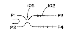
この図25に示した帯域通過フィルタにおいて、ポートP1から入力された光は3dBカプラ105で2分岐される。グレーティング102の反射中心波長λcと等しい波長の光、すなわち信号光はグレーティング102で反射されて再度3dBカプラ105で合波されてポートP2から出力される。グレーティングの反射中心波長λcと異なる波長の光、すなわちノイズ光はグレーティング102を透過してポートP3,4から出力される。このようにして、図25の帯域通過フィルタは、ノイズ光をカットし、信号光のみをポートP2から取り出すことができる。
【0006】
また、図26は導波路グレーティングを利用した合分波回路の一例を示すものである。この図26の従来例の合分波回路において、例えば種々の異なる波長の信号(λ1,λ2,λ3,・・・)がポートP1から入射されると、ある特定の波長の信号光のみ(図ではλ1)がグレーティング102で反射されてポートP2から出力される(分波)。それ以外の波長の信号光(λ2,λ3,・・・)はポートP4から出力される。またポートP3から入力された特定の波長の信号光(λ1の波長を有する光)はグレーティング102で反射されてポートP4から出力される(合波)。
【0007】
図27は導波路グレーティングを利用した分散補償器の一例を示すものである。光通信において、光信号の伝送媒体となる光ファイバは、屈折率が波長によって異なる分散を有しているため、光の波長によって伝送路を伝搬する速度が異なり、波長ごとに群遅延量が異なる。光パルス信号は波長成分に広がりを有するため、波長による群遅延差により数十キロ伝搬すると、図28に示すように、信号に広がりが生じてしまう(図28において、(a)は伝搬前の信号波形を示し、(b)は伝搬後の波形を示している。)。それ故、超高速光通信では光ファイバの分散を補償する技術が必要となる。
【0008】
光ファイバを伝搬するときの、波長と群遅延の関係は図29(a)に示すようになり、その微分で表される分散は図29(b)のように表される。よってこれを補償するためには図30(a)(b)にそれぞれ示すような群遅延と分散を有するデバイスが必要となり、これは、図27に示す分散補償器により実現できる。この分散補償器の導波路グレーティング102は、入力ポート側から離れるほどその周期が長くなるように形成されている。このように周期を変化させて形成することにより、光の波長により反射位置が異なり、図30(a)に示すようにのように群遅延に傾きが生じる。すなわち分散が図30(b)に示すように正の一定値となり、光ファイバの分散値と符号が逆になるために分散補償が可能となる。
【0009】
また、図31は導波路グレーティングを利用した可変分散補償器の一例を示すものである。分散補償器に要求される分散値(補償すべき分散値)は、伝送路として用いる光ファイバの長さや使用される状況等により異なるために、補償する分散値が固定された分散補償器を用いる場合、補償する分散値の異なる複数の分散補償器を準備してそれぞれ挿入してみて、最適なものを選択していた。これに対して、図31の可変分散補償器では分散値の微調整が可能であるため、最適化のための試行錯誤が必要になるという問題点を解決することが可能である。すなわち、図31に示す可変分散補償器において、温度印加手段24a,24bによって光導波路に熱が印加される。このとき温度印加手段24aと温度印加手段24bが発生する熱量を異なる値とすることで、導波路グレーティングに熱勾配を生じさせる。
【0010】
導波路グレーティングの等価屈折率neffは温度の関数となっているため温度印加手段24a,24bによって互いに異なる熱が印加されることによって生じさせた熱勾配は、光導波路の等価屈折率neffを導波路長手方向に対して傾斜させる。このようにすると、(1)式に示されるように反射中心波長はneffの関数となるため、導波路グレーティングの長手方向の位置によって反射中心波長が変化することになる。従って、熱勾配によっていわゆるチャープドグレーティングと同様な効果が生じ、波長に対応して反射点までの距離が異なるようになり、分散が発生する。このようにすると、温度勾配と群遅延及び分散の関係は図32(a)(b)(c)に示すようにでき、温度印加手段による温度勾配の変化により分散値の調整が可能となる。
【0011】
次に、以上の光デバイスに利用される導波路グレーティングの作製方法について説明する。導波路グレーティングの作製方法の代表的なものとしては、光誘起屈折率変化を利用したものが挙げられる。尚、光誘起屈折率変化とは、ゲルマニウムを添加した石英系導波路に紫外光を照射すると屈折率が変化する現象のことである。具体的には、導波路上に2つの紫外光を干渉させて干渉縞を形成すると、干渉縞の周期に対応した屈折率変化が生じ、導波路グレーティングが作製される。これによる屈折率の変化は0.001程度の小さなものであるが、グレーティングの周期が500nm程度と非常に小さいため、1cm程度の長さにすると、20000周期程度の導波路グレーティングを作製することができ、反射中心波長において簡単に概ね100%の反射率が得られる。
【0012】
このようにして作製された導波路グレーティングにおいて、グレーティング周期に製造バラツキがあるために、グレーティングの反射中心波長には一定のバラツキが存在する。また、導波路グレーティングの作製において、紫外光強度や照射時間が大きくなったり、セッティング等の条件により導波路グレーティングが導波路の光の進行方向の直角方向に対して傾いて作製されたりすると反射中心波長は大きくなる。従って、反射中心波長を調整する工程が必要であり、従来は導波路グレーティングを作製した後に、反射中心波長を測定して、所望の反射中心波長と異なる場合には紫外光を導波路グレーティングにさらに照射する方法(特開平9−288205号公報)、あるいは加熱処理を行う方法(特開平10−339821号公報)等を用いて反射中心波長を調整していた。
【0013】
また石英系の材料を用いた導波路の実効屈折率neffは温度により変化し、それに伴い反射中心波長λcも式(1)に従い図32(c)に示すように変化する。通常、石英系導波路上に作製したグレーティングでは、0.01nm/℃の割合で変化する屈折率を有しているので、帯域通過フィルタ、合分波器、分散補償器では、温度の変化により反射中心波長が変化しないように対策する必要がある。この温度変化により反射中心波長が変化するという問題は、材料そのものの温度特性に起因して発生するものであるために、従来は、ペルチェ素子等を用いて温度制御をしたり、導波路の屈折率とは逆符号の温度係数を持つ光学媒質を導波路上に被着する(特開平10−186167号公報)等の方法により反射中心波長の変化を防止していた。また、1999年電子情報通信学会総合大会において、荒井等により、「導波路型Add/Dropフィルタの温度特性補償」(C−3−98)と題して、導波路を形成した基板と比較して熱膨張係数の大きな金属板等を基板に接着するなどの手法が提案されている。
【0014】
【発明が解決しようとする課題】
しかしながら、紫外光を導波路グレーティングに再照射する方法や加熱処理を行う方法は、調整に時間がかかり安価に製造することができないという問題点があった。
また、温度特性を改善する(温度の変化による反射中心波長の変化を小さくする)構造に関しては、ペルチェ素子等を用いて温度制御する構造、導波路の屈折率とは逆符号の温度係数を持つ光学媒質を導波路上に被着する構造、基板と比較して熱膨張係数の大きな金属板等を基板に接着する構造のいずれの構造も、構造が複雑で製造に時間がかかるという問題点があった。
【0015】
そこで、本発明は、作製した後にその反射中心波長を従来例に比較して簡便に制御することができる導波路グレーティングデバイスを提供することを第1の目的とする。
また、本発明は、温度の変化による反射中心波長の変化を小さくすることができる導波路グレーティングデバイスを提供することを第2の目的とする。
さらに、作製した後にその反射中心波長を簡便に調整することができる導波路グレーティングの反射中心波長調整方法を提供することを第3の目的とする。
【0016】
【課題を解決するための手段】
以上の目的を達成するために、本発明に係る導波路グレーティングデバイスは、ブラッグ波長を有する導波路グレーティングを有する基板と、上記導波路グレーティングに接続された光導波路と、ケースと、上記基板の第1の主面に接して上記基板を上記ケース内で支持する基板支持体と、上記ケース内に設けられ、上記第1の主面とは反対側の上記基板の第2の主面に接し、上記基板と直交する方向に移動可能、又は固定された基板押圧手段と、を備え、
上記基板押圧手段によって上記基板を撓ませて固定し、
上記基板支持体もしくは基板押圧手段、又は上記基板支持体及び上記基板押圧手段の両方が、温度の変化に対応して変化する該導波路グレーティングの反射中心波長の変化を打ち消す熱膨張係数を有し、
上記基板押圧手段は、それぞれ基板に接する第1と第2の先端表面を有し、かつ該第1と第2の先端表面が上記導波路グレーティングを跨ぐように設けられた荷重分割部を先端部に有することを特徴とする。
以上のように構成することにより、簡単な構成で温度補償できる。
【0017】
また、本発明に係る導波路グレーティングデバイスは、荷重の集中を緩和するために、上記基板支持体の先端表面を上記基板と線状に接するようにすることが好ましい。
【0018】
また、本発明に係る導波路グレーティングデバイスにおいて、上記基板支持体は、荷重の集中を緩和するために、上記基板に平行な一直線を軸として曲率を有する円弧形状の先端表面を有し、その先端表面で上記基板と線状に接するようにすることがさらに好ましい。
【0019】
また、本発明に係る導波路グレーティングデバイスでは、上記基板押圧手段の先端部に、それぞれ基板に接する第1と第2の先端表面を有し、かつ該第1と第2の先端表面が上記導波路グレーティングを跨ぐように設けられた荷重分割部を設けるようにしている。これにより、荷重に対して基板の導波路グレーティングが形成された部分に生じる応力をほぼ均一に発生させることができる。
【0020】
さらに、本発明に係る導波路グレーティングデバイスでは、上記導波路グレーティングが形成された基板の表面もしくは反対側の表面が有機材料によりコートされていることが好ましい。
【0021】
また、本発明に係る導波路グレーティングデバイスでは、上記有機材料によるコートに代えて、上記ケース内に上記基板を気密封止するようにしてもよい。
【0022】
【発明の実施の形態】
以下、図面を参照しながら、本発明に係る実施の形態について説明する。
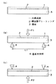
まず、個々の実施の形態を説明する前に、図1〜図4を用いて、本発明の原理について説明する。以下の説明において、1は光導波路、2は導波路グレーティング、3は基板、4は基板支持部である。
図1(a)に示すように、導波路1の一部分の屈折率を周期的に変化させてなる導波路グレーティング2が形成された基板3を、図1(b)に示すように基板支持部4を用いて支持し、基板3の上面から外力(応力)をかけると基板が撓み導波路グレーティング2のグレーティング周期Λが小さくなり、従来技術の項で示した(1)式により表される反射中心波長は小さくなる。またこれとは逆に、図1(c)に示すように外力(応力)をかけることにより反射中心波長は大きくなる。
【0023】
図1(b)(c)に示す方向に応力をかけたときの、反射中心波長と応力との関係をそれぞれ図2(a),(b)に示す。このようにして、応力のかけ方によりグレーティング周期Λを縮めたり伸ばしたりできるので、反射中心波長を任意に調整することが可能である。また、基板支持部4間の距離L1と基板の厚みt1の比t1/L1が小さくなるほど図2の直線の勾配は急となり、同じ応力に対する反射中心波長の変化量を大きくできる。実際にはt1/L1<0.2とならないと応力に対する反射中心波長の変化量を大きくできないので、t1/L1<0.2とすることが好ましい。
【0024】
また、温度が変化すると導波路グレーティング2の部分の実効屈折率が変化し、(1)式により表される反射中心波長の温度による変化は、図3のようになる。従って、温度変化とともに印加する応力を適度に変化させることにより、実効屈折率の変化量を印加する応力により打ち消すようにすると、温度特性を補償して図4に示すように、温度の変化に対する反射中心波長が変化しないようにできる。
以下、図面を参照しながら、反射中心波長制御(調整)及び温度特性補償に関する具体的な構成を各実施の形態において説明する。
【0025】
実施の形態1.
本発明に係る実施の形態1の導波路グレーティングデバイス12は、信号光の波長の光を通過させる帯域通過特性を有し信号光に含まれるノイズを除去する帯域通過フィルタ(BPF)であって、導波路グレーティング2の反射中心波長を調整するための応力調整用スクリュー8を備えたことを特徴としている。
【0026】
すなわち、実施の形態1の導波路グレーティングデバイス12においては、図5に示すように、一対の導波路1と3dBカプラ5と導波路グレーティング2が形成された基板3が、ケース7の底面に所定の間隔を隔てて設けられた2つの基板支持部4を用いて支持され、ケース7の上部板には、応力付加手段として応力調整用スクリュー(基板押厚手段)8が2つの基板支持部4の間で基板3に接するように設けられている。このようにして、実施の形態1では、導波路グレーティングデバイス12を作製した後に、ケースに設けられた応力調整用スクリュー8で基板3に外力を加えて導波路グレーティング2の反射中心波長を調整することにより、フィルタの帯域通過特性を調整することができるようにしたことを特徴としている。
【0027】
以下、本実施の形態1の導波路グレーティングデバイス12の各構成要素について図5(a)(b)を参照して詳細に説明する。
導波路1は、例えば、ゲルマニウムを添加した石英系の導波路を基板3の上面に互いに線対称となるように1対形成される。尚、2つの導波路1の一部を互いに近接するように形成して3dBカプラ5を導波路の一部を用いて形成する。
導波路グレーティング2は、例えば、紫外光を用いて各導波路の一部にそれぞれ干渉縞を形成することにより、所定の周期で屈折率を変化させて、それぞれの導波路1の一部に形成される。尚、導波路グレーティング2は、互いに線対称となるように各導波路1にそれぞれ形成される。
【0028】
ファイバコネクタ6は、導波路1の各一端に接続され、基板3の一端に固定される。
基板支持部4は、ケース1の底面に所定の間隔を隔てて設けられる。
その基板支持部4により、導波路1、3dBカプラ5及び導波路グレーティング2が形成されかつファイバコネクタ6が設けられた基板3がその下面で支持される。
ここで、基板支持体4は、基板3と線で接触するように構成され、基板支持体4の基板3と接する先端部分は基板3に平行な軸について曲率を有する円弧形状とすることが好ましい。
応力調整用スクリュー8は、基板支持部4によって固定された基板3を導波路グレーティング2が形成された部分で撓ませることができるように、スクリューの先端が基板3の上面に接するようにケース7の上部板に取りつけられる。
基板押圧する手段である応力調整用スクリュー8の先端部分は、荷重を1点に集中させないように、1点を中心として曲率を有する円弧形状、又は基板3と平行な一つの直線を軸として曲率を有する円弧形状とすることが好ましい。
【0029】
以上のように構成された実施の形態1の帯域通過フィルタにおいて、ポートP1から入力された光は3dBカプラ5で2分岐される。2分岐された光のうち、導波路グレーティング2の反射中心波長λcの光、すなわち信号光は導波路グレーティング2で反射されて再度3dBカプラ5で合波されてポートP2から出力される。グレーティングの反射中心波長以外の光すなわちノイズ光はグレーティングを透過してポートP3,4から出力される。このように帯域通過フィルタはノイズ光をカットし、信号光のみを取り出す機能を有する。
【0030】
本実施の形態1の帯域通過フィルタでは、導波路グレーティング2が形成された部分に応力調整用スクリュー8により外力を印可できる構造となっており、図5に示した構成では、印可した外力により基板3を撓ませてその撓み量に応じて導波路グレーティング2の周期を小さくして、その反射中心波長を小さくして所望の値に調節することができる。
また、導波路グレーティング2の反射中心波長を製造時(調整前)より大きくすることにより調整する場合には、図5の構成において、導波路1が形成された表面を下にして基板3を基板支持部4にセットして応力調整用スクリュー8により外力を印加して反射中心波長を調整するようにすればよい。
【0031】
すなわち、本実施の形態1の帯域通過フィルタの構成では、導波路グレーティング2の反射中心波長(フィルタの通過帯域の中心周波数)が所望値より大きい場合には、導波路1が形成された表面を上(応力調整用スクリュー8と対向する側)になるように基板3を基板支持部4により支持して、応力調整用スクリュー8により外力を印加して基板を撓ませてグレーティング周期を小さくすることにより反射中心波長を調整する。
また、導波路グレーティング2の反射中心波長(フィルタの通過帯域の中心周波数)が所望値より小さい場合には、導波路1が形成された表面を下(応力調整用スクリュー8と反対側)になるように基板3を基板支持部4により支持して、応力調整用スクリュー8により外力を印加して基板を撓ませてグレーティング周期を大きくすることにより反射中心波長を調整する。
例えば、所望の反射中心波長が1553.0nmである帯域通過フィルタを製造する場合において、調整前の帯域通過フィルタの反射中心波長が1552.5nmである場合には、導波路1が形成された表面を下にして基板3を基板支持部4により支持して、応力調整用スクリュー8により外力を印加して反射中心波長を調整する。
【0032】
帯域通過フィルタの反射中心波長の調節は図6に示す光学測定系を用いて行うことができる。
本光学測定系では、広帯域光源9として例えば、EDFA(Erbium-Doped Fiber Amplifier)の自然放出光を用いることができ、その広帯域光源9から放出される光を光アイソレータ11を介してポートP1から帯域通過フィルタに入力し、ポートP2から出力される光を光アイソレータ11を介してスペクトルアナライザ10に入力して波長特性を観測する。
製造時より反射中心波長を大きくして調整する場合の一例を示すと、図7のようになる。すなわち、応力調整用スクリュー8を回して外力を印加することにより反射中心波長を長波長側にシフトさせることができ、所望の反射中心波長が得られた位置でスクリュー8を固定する。実施の形態1の構成及び図6の測定系を用いて、精度は±0.01nm程度で、非常に精密に合わせることができる。
【0033】
次に、ケース7内における、基板支持部4による基板3の支持(固定)方法について説明する。
上述したように、本発明に係る実施の形態1では、基板3を撓ませることにより、導波路クレーティング2の中心波長を変化させている。従って、本実施の形態1では、ケース7内に、基板3の荷重による撓みを阻害することなく、基板3を固定する必要がある。
ケース7内における基板支持部4と基板3との固定方法として接着剤等を用いて接着する方法が考えられるが、本発明者らの検討によれば、基板支持部4と基板3及び応力調整用スクリュー8と基板3とをそれぞれ接着すると、荷重による中心波長の変化量が極めて小さいことが明らかになった。
【0034】
図8は、基板支持部4と基板3及び応力調整用スクリュー8と基板3とをそれぞれ接着した場合と接着しない場合とにおける、荷重に対する中心波長の変化を示すグラフである。
ここで、本検討では、基板3は厚さが1mmのものを用い、2つの基板支持部4の間隔は14mmとして図8に示す結果を得た。
図8から明らかなように、基板支持部4と基板3及び応力調整用スクリュー8と基板3とをそれぞれ接着すると、荷重に対する中心波長の変化量が極めて小さくなる。
そこで、本実施の形態1においては、図9に示すように、所望の中心波長に設定した時に、基板に所定の荷重がかかるようにして基板を撓ませ固定している。
尚、本実施の形態1では、1000g(1kg)の荷重をかければ、実用上十分な固定が可能である。
【0035】
図10は、荷重に対する中心波長のシフト量を示すグラフであり、基板3の厚さhが、0.52mmの場合、0.71mmの場合、1.0mmの場合についてそれぞれ、理論値と実測値とを示している。
図10から、所望の中心波長が1555.0nmである導波路グレーティングデバイスを0.7mmの厚さの基板を用いて構成する場合、荷重をかけていない場合の反射中心波長が1555.7nmになるように基板を作製すれば、約1kgの荷重をかけた時に所望の波長にできかつ接着することなくケース7内に基板3を固定することができる。
尚、図10において、基板3を導波路グレーティングが形成された表面を基板支持体4に対向させて支持した時における基板を撓ませるための荷重を正とし、基板3を導波路グレーティングが形成された表面を応力調整用スクリュー8に対向させて支持した時における基板を撓ませる荷重を負として表した。
【0036】
また、以上のように、本実施の形態1では、基板支持部4と基板3及び応力調整用スクリュー8と基板3とをそれぞれ接着することなく、荷重をかけることにより基板3を固定しているので、基板支持部と基板3とを以下のような形状にしてより確実に基板3を固定することが好ましい。
図11(a)(b)は、基板3を固定する凹部4cを有する基板支持部4aを用い、その凹部4cに基板3を嵌め合わせた例(第1の例)を示している。
また、この第1の例では、基板支持部4aの内側に接するように、基板3の下面に凸部3aを設け基板3の固定をより確実にしている。
以上のように構成された基板支持部4aと凸部3aを有する基板3とを用いて構成することにより、荷重による基板3の撓みを阻害することなく、より確実に固定することができる。
【0037】
また、図11(c)(d)は、凹部4cを有する基板支持部4aを用いた他の例(第2の例)を示すものである。この第2の例では、基板支持部4aの外側に接するように、基板3の下面に凸部3bを設け基板3の固定をより確実にしている。
以上のように構成された基板支持部4aと凸部3bを有する基板3とを用いて構成しても、荷重による基板3の撓みを阻害することなく、より確実に固定することができる。
【0038】
また、図12(a)(b)は、図11と同様、凹部4cを有する基板支持部4aを用いた他の例(第3の例)を示すものである。この第3の例では、基板支持部4aの凹部にかみ合うように、基板3の下面に溝3cを設け基板3の固定をより確実にしている。
以上のように構成された基板支持部4aと溝3cを有する基板3とを用いて構成しても、荷重による基板3の撓みを阻害することなく、より確実に基板3を固定することができる。
【0039】
またさらに、図12(c)(d)は、基板3の両側において閉じた溝3dを基板3の下面に形成し、その溝3dに基板支持部4bをかみ合わせることにより、基板支持部4bにより基板3を支持するようにした例を示している。
以上のようにしても、上述の第1〜第3の例と同様、荷重による基板3の撓みを阻害することなく、より確実に基板3を固定することができる。
【0040】
以上のように構成された実施の形態1の帯域通過フィルタ(導波路グレーティングデバイス)は、帯域通過フィルタの反射中心波長を製造時の最終段階(組み立てが終了した段階)で簡便に調整することができ、歩留まりを向上させることができるとともに、コストを低減することができる。
【0041】
また、本実施の形態1では、基板支持部4と基板3及び応力調整用スクリュー8と基板3とをそれぞれ接着することなく、荷重をかけることにより基板3を固定しているので、帯域通過フィルタの反射中心波長の調整量を大きくすることができ、より歩留まりを向上させることができ、さらにコストを低減することができる。
また、図11及び図12に示す固定構造を採用することにより、より確実にケース7内に基板3を固定することができ、耐振動性等の信頼性を向上させることができる。
尚、図11及び図12に示す固定構造は、後述する他の実施の形態にも採用することができ、それらの各実施の形態において、耐振動性等の信頼性を向上させることができる。
【0042】
実施の形態2.
本発明に係る実施の形態2の導波路グレーティングデバイスは、実施の形態1の帯域通過フィルタ(BPF)において、導波路グレーティング2の反射中心波長を調整するための応力調整用スクリュー8を所定の熱膨張係数を有する材料で構成することにより周囲温度の変化に対応させて導波路グレーティング2にかかる応力を変化させ、温度による反射中心波長の変化を補償できるようにしたものである。実施の形態2の帯域通過フィルタにおいて、上述以外の点は実施の形態1と同様に構成される。
【0043】
具体的には、例えば、温度特性を補償しない場合に、温度と反射中心波長の関係が図3に示すようになった場合、これを補償するために、応力調整用スクリュー8及び基板支持部4の熱膨張係数がケース7に比較して大きくなるように材料を選択する。このように構成すると、温度が高くなるとケース7に比較してスクリュー8と基板支持部4が大きく膨張するので、基板の導波路グレーティング2が形成された部分に印加される曲げ応力は強くなり、図2(a)に示すように反射中心波長が小さくなる方向へ働くために温度特性を補償することができる。本実施の形態2において、応力調整用スクリュー8及び基板支持部4の材料としてポリスチレンを用い、ケース7の材料としてアルミニウムを用いることができる。
【0044】
応力調整用スクリュー8及び基板支持部4の材料としてポリスチレンを用い、ケース7の材料としてアルミニウムを用いた、本実施の形態2に係る帯域通過フィルタの一例を以下に示す。
まず、本例では、室温での所望の反射中心波長1545.0nmに対し、応力印加前の反射中心波長は1545.2nmであった。このように所望の反射中心波長に対して、0.2nmだけ大きかったため、導波路が形成された表面を上に向けて基板をケース7にセットした。その後、図13の光学測定系において恒温槽14の温度を25℃にして、反射中心波長を観測しながら応力調整用スクリュー8を回転させて、反射中心波長を1545.0nmになるように調整した。
【0045】
次に恒温槽14の温度を変えながら反射中心波長を観測した。その結果、温度に対する反射中心波長の変化率は、10℃〜80℃において0.002nm/℃であり、従来と比較して1/5に低減された。
【0046】
以上のように構成された実施の形態2の帯域通過フィルタは、実施の形態1と同様の作用効果を有するとともに、さらに温度特性の向上させることができる。
【0047】
実施の形態3.
本実施の形態3の帯域通過フィルタは、実施の形態2の帯域通過フィルタにおいて、導波路1が形成された表面を下(応力調整用スクリュー8と反対側)になるように基板3を基板支持部4により支持した以外は実施の形態2と同様に構成される。
このようにセットすることにより、導波路グレーティング2の反射中心波長が所望の値と比べて小さな場合に、応力調整用スクリュー8で曲げ応力を印加することにより反射中心波長を大きくでき所望の値に調節できる。
【0048】
また、実施の形態3の構成において、温度特性を補償しない場合は、温度と反射中心波長の関係は図3のようになる。これを補償するために、ケース7の熱膨張係数がスクリュー8及び基板支持部4と比較して大きくなるように材料を選択する。このような構成では、温度が高くなり、ケースの側面が膨張すると導波路に印加される応力は弱まり、図2(b)に示すように反射中心波長が小さくなる方向へ働くために温度特性が補償される。本実施の形態3ではケース7にポリスチレンを用い、スクリュー8及び基板支持部4にアルミニウムを用いることができる。尚、ここではケース7全体をポリスチレンとしてもよいし、ケース側面のみにポリスチレン等の熱膨張係数の大きい材料を使用するようにしてもよい。
【0049】
以下に本実施の形態3に係る一例を示す。
本例では、室温での所望の反射中心波長1556.5nmに対し、応力印加前の反射中心波長は1556.2nmと、0.3nmだけ小さかった。そのため、導波路が形成された表面を下に向けて基板3をケース7に配置した。その後、図13に示す光学測定系において恒温槽の温度を25℃とし、反射中心波長を観測しながら応力調整スクリュー8を回転させて、反射中心波長が1556.5nmとなるように調整した。次に恒温槽の温度を変えながら反射中心波長を観測した。その結果、温度に対する反射中心波長の変化率は−20℃〜50℃において0.002nm/℃と、従来と比較して1/5に低減することができた。
以上のように、本実施の形態3の帯域通過フィルタは、実施の形態2と同様の作用効果を有する。
【0050】
実施の形態4.
本実施の形態4の帯域通過フィルタは、図14に示すように、以下の点が実施の形態1の帯域通過フィルタとは異なり、他の部分は実施の形態1と同様に構成される。
実施の形態1と異なる点
(1)導波路1が形成された表面が基板支持部4に接するように基板3を基板支持部4上に配置した。
(2)実施の形態1の応力調整スクリュー8に代えて、後述する比較器18の出力端子が接続された応力調整用アクチュエータ20を用いて構成した。
(3)ケース7内の導波路グレーティング2に近接して設けられた温度検出素子16と、その検出素子16に接続された例えばサーミスタや半導体デバイスなどからなる温度検出回路17と、温度検出回路17の出力端子が負側の入力端子に接続され正側の入力端子に基準電圧発生回路19が接続された比較器18とからなる応力制御回路を備えた。
【0051】
以上のように構成された実施の形態4の帯域通過フィルタは、導波路グレーティング2にアクチュエータ20により応力を印加できる構造となっており、反射中心波長を所望の値に調節できるのみならず、周囲温度の変化とともに導波路グレーティング2にかける曲げ応力を変化させることができ、温度による反射中心波長の変化を補償することができる。
【0052】
次に、本実施の形態4における応力制御回路の動作を説明する。
温度検出回路17は、温度検出手段16により計測された温度を電圧に変換して比較器18の負側の入力端子に入力する。また、基準電圧発生回路19は、基準電圧を比較器18の正側の入力端子に入力する。比較器18は、温度検出回路17から入力される電圧と基準電圧とを比較して誤差信号をアクチュエータ20に入力する。このようにして、アクチュエータ20は導波路グレーティング2の周辺の温度に基いて温度によって変化するグレーティングの反射中心波長を補償するように制御される。
【0053】
以下に、本実施の形態4に係る帯域通過フィルタの一例を示す。
まず、図14に示す構成の帯域通過フィルタを作製したところ、所望の反射中心波長1555.1nmに対し、応力印加前の反射中心波長は1554.7nmと、0.4nm小さかった。そこで、導波路1が形成された基板の表面を下に向けてケース7にセットした。そして、図13の光学測定系を用いて、恒温槽14の温度25℃において反射中心波長を観測しながら、基準電圧発生回路19の電圧を変えて反射中心波長を調整した。調整した結果1555.1nmとなった。
次に恒温槽14の温度を変えながら反射中心波長を観測した。その結果、温度に対する反射中心波長の変化率は0.001nm/℃と、従来と比較して1/10に低減されていた。
このように本実施の形態4の帯域通過フィルタは、反射中心波長の簡便な制御と、さらには温度特性の向上に有効であることが確認できた。
【0054】
実施の形態5.
図15は本発明に係わる実施の形態5の導波路グレーティングデバイスの平面図(a)及び断面図(b)である。この実施の形態5の導波路グレーティングデバイスは波長可変型合分波回路としての機能を有する。
実施の形態5において、まず、基板3に1対の導波路1が対称に形成される。
ここで、導波路1は、所定の間隔を隔てた2箇所において互いに近接するように形成し、その近接部分により3dBカプラ5a,5bを構成する。
また、3dBカプラ5a,5bの間の導波路1にそれぞれ導波路グレーティング2を形成する。尚、導波路1は基板3一端及び他端においてファイバコネクタ6に接続される。
【0055】
以上のように、導波路1、3dBカプラ5a,5b及び導波路グレーティング2が形成された基板3をケース7の底面に所定の間隔を隔てて設けられた基板支持部4上により支持する。
【0056】
尚、本実施の形態5では、図15(a)に示すように、導波路グレーティング2が形成された領域の基板の厚みを比較的小さな力で撓むように研磨により薄くしている。われわれの検討によれば、研磨した領域の導波路長手方向の長さをL2とし、基板の厚みをt2とした場合、その比がt2/L2<0.5を満足するようにt2,L2を設定すると、比較的小さな力で効果的に基板3を撓ませることができ、応力調整用アクチュエータ20に印加する電圧に対する反射中心波長の変化を実用的な範囲にできる。
また、t2/L2は小さくなるほど、電圧に対する反射中心波長の変化の勾配は図20に示すように急になる。しかしt2を薄くしすぎると機械的強度が保たれなくなるために反射中心波長のシフト量が数nm程度になるように応力を印加したところで基板3は破壊されてしまうので、研磨後の基板の厚さは必要な反射中心波長の変化量と基板3の機械的強度を考慮してその最適値が決定される。
【0057】
以上のように成された実施の形態5の導波路グレーティングデバイス72である波長可変型合分波回路において、数種類の波長(λ1,λ2,λ3,・・・)を有する信号は、ポートP1から入射され、(1)式に対応した特定の単一波長の信号光のみ(λn)が導波路グレーティング2により反射されてポートP2から出力され(分波)、それ以外の波長の信号光はポートP4から出力される。またポートP3から入力された特定の波長の信号光(λn)は導波路グレーティング2で反射されてポートP4から出力される(合波)。
【0058】
ここで、特に実施の形態5の波長可変型合分波回路では、導波路グレーティング2の反射中心波長はアクチュエータ20により任意に選択できるという特徴を有している。すなわち、アクチュエータ20に電圧をかけることにより導波路グレーティング2に曲げ応力が印加され、グレーティング周期が長くなり反射中心波長は(1)式に従い変化する。電圧と反射中心波長の関係は図16に示すようになるので、電圧を変化させることにより合波及び分波する波長を任意に選択できる。すなわち、電圧V1の際には図17(a)に模式的に示すようにλ1の光信号を合分波でき、電圧V2の際にはλ2の光信号を合分波できる。
【0059】
本実施の形態5に係る1つの例として、導波路グレーティング2が形成された領域の基板の厚みt2を研磨により0.5mmとし、研磨した領域の導波路長手方向の長さL2とt2の比はt2/L2=0.1としたものを作製した。
尚、本実施の形態5では、研磨することにより基板3の厚さを薄くしたが、本発明はこれに限らず、エッチング等の技術を用いて薄くするようにしても良い。
従来、基板上に形成された導波路グレーティングを利用した合分波回路では、反射中心波長が固定されたものしかなかったが、本実施の形態5の合分波回路により反射中心波長をアクチュエーターにより変化させることができる合分波回路が提供できるようになる。
【0060】
実施の形態6.
実施の形態6の合分波回路は、図19に示すように、実施の形態5の合分波回路において導波路グレーティング2が形成されかつ薄く研磨された部分に有機材料層21を形成して、薄くした基板の撓みを阻害しないようにその部分の機械的強度を強くした点が実施の形態5とは異なり他の部分は実施の形態5と同様に構成される。
【0061】
このように構成することで、本実施の形態6では導波路グレーティング存在する領域の基板の厚みt2を研磨により0.1mmとすることができ、研磨した領域の導波路長手方向の長さL2とt2の比はt2/L2=0.01とすることができた。尚、基板を薄くするためには、研磨に代えてエッチング等の技術を用いても良い。また、有機材料層21は、スピンコーティング等により導波路が形成された基板3の表面、該表面の反対側の表面及び基板側面にそれぞれ0.5mmづつポリメチルメタクリレート(PMMA)等を成膜することにより形成することができる。
【0062】
具体的には、PMMAのクロロフォルム溶液に電化移動型カルバゾール、可溶化フタロシアニンを溶解し、その溶液をスピンコーターにセットされた導波路の表面に滴下した。遠心力により表面において薄い液層となり、溶液が蒸発するとPMMAの膜が形成される。
このようにすることで、本実施の形態6の合分波回路では、実施の形態5と同様、アクチュエータ20により応力を印加することで反射中心波長を可変とすることができ、実施の形態5に比較してさらに基板を薄くして有機材料をコーティングしたことにより可変範囲を20nmと非常に大きくすることができる。
【0063】
実施の形態7.
本発明に係る実施の形態7の導波路グレーティングデバイスは、図33に示すように、実施の形態1の帯域通過フィルタにおいて、導波路グレーティング2に代えて、徐々にグレーティング周期が大きくなるように形成された導波路グレーティング2aを用いて構成し、分散補償器として機能させたものである。上述以外は実施の形態1と同様に構成される。
【0064】
本実施の形態7の分散補償器において、ポートP1から入力された光は3dBカプラで2分岐される。導波路グレーティング2aの反射中心波長λcの光すなわち信号光は導波路グレーティング2aで反射され再度3dBカプラで合波されてポートP2から出力される。ここで、特に分散補償器では、光ファイバーによる負の分散を打ち消す正の分散を得るためには上述のように導波路グレーティングの周期を入射ポート側から離れるに従い大きくしているので、導波路グレーティングの周期の変化に対応した分散特性を有する。
【0065】
すなわち、光ファイバーを伝送する光パルス信号は、λcを中心として多少波長広がりが生じているため、伝送前において図20(a)に示すような波形をしていた光パルス信号は、光ファイバを数十キロ伝搬した後においてはファイバの分散により図20(b)に示すように、時間的に広がりを生じる。これを補正するために、光ファイバの分散が図29に示すように負の値になっているのに対し、分散補償器の分散は正の値となっており、両者の分散を合わせてゼロになるようにグレーティングの周期を入射ポート側から離れるに従い大きくしている。
これによって、数十キロのファイバを伝搬したことにより広がった光パルス信号は、分散補償器を通過することにより図20(c)に示すような波形にでき、光ファイバを伝送する前の波形に補正される。
【0066】
本実施の形態7の分散補償器は、導波路グレーティング2にスクリュー8により応力を印加できる構造となっており、反射中心波長を所望の値に調節できる。本実施例では導波路が形成された基板の表面が応力調整用スクリュー8に接するようにセットしており、また応力調整用スクリュー8、基板支持部4、ケース7が適当な熱膨張係数を有し、周囲温度の変化とともに導波路グレーティング2にかかる応力が変化し、温度による反射中心波長のシフトを補償できるようになっている。
温度特性を補償しない場合は、温度と反射中心波長の関係は図3のようになるが、これを補償するために、応力調整スクリュー8及び基板支持部4の熱膨張係数をケース7と比較して大きくなるように材料を選択する。このように構成すると、温度が高くなって応力調整スクリュー8及び基板支持部4が膨張すると導波路グレーティング2に印加される応力が強くなり、図2(a)より反射中心波長が小さくなる方向へ働くために温度特性が補償される。
【0067】
本実施の形態7の具体例としてはケース7にアルミニウムを用い、スクリュー8及び基板支持部4にポリスチレンを用いた。
作製したものが、室温での所望の反射中心波長1551.0mに対し、応力印加前の反射中心波長は1552.0nmと、1.0nm大きかったため、導波路表面をスクリュー側に向けてケースにセットした。そして、図13の光学測定系において恒温槽14の温度を25℃とし、反射中心波長を観測しながらスクリューを回転させて、反射中心波長が1551.0nmとなるように調整した。精度は±0.01nm程度で、非常に精密に合わせることができた。
【0068】
従来はある決められた反射中心波長の分散補償器を作製するのは難しかったが、本実施の形態7の分散補償器により一度作製した分散補償器の反射中心波長を非常に簡便に調整することが可能となり、製造歩留まりを向上させることができ、コスト低減が可能となる。さらに本発明は温度特性の向上に有効であることが確認できた。
【0069】
実施の形態8.
本発明に係る実施の形態8の導波路グレーティングデバイスは、可変分散補償器であって、図21は、その可変分散補償器の分散特性を変化させる構成を説明するための模式的なブロック図であり、図22はその可変分散補償器の反射中心波長の調整及び温度特性の調整方法を説明するための模式的なブロック図である。
本実施の形態8の可変分散補償器は、
(1)図21に示す導波路グレーティング2の両側に設けられた導波路グレーティング2に熱勾配を形成する温度印加手段24と、各温度印加手段に接続された、温度検出回路17、基準電圧発生器19及び比較器18からなる熱勾配制御回路を備え、
(2)実施の形態7の応力調整スクリュー8に代えて、比較器18の出力端子が接続された応力調整用アクチュエータ20を用い、
(3)ケース7内の導波路グレーティング2に近接して設けられた温度検出素子16と、その検出素子16に接続された例えばサーミスタや半導体デバイスなどからなる温度検出回路17と、温度検出回路17の出力端子が負側の入力端子に接続され正側の入力端子に基準電圧発生回路19が接続された比較器18とからなる応力制御回路を備えた点が実施の形態7の可変分散補償器とは異なり、他の部分は実施の形態7と同様に構成される。
【0070】
この実施の形態8の可変分散補償器は、実施の形態7の可変分散補償器と同様の機能を有しさらに以下のような特徴を有する。
すなわち、分散補償器に要求される分散値は、ファイバの長さや使用される状況等により異なり、従来はいくつもの異なる分散値を有する分散補償器を挿入してみて、最適なものを選択していたので、その選択に非常に手間がかかっていた。しかし本実施の形態8の可変分散補償器によれば、選択にかかる手間を無くすことができる。
【0071】
すなわち、本実施の形態8の可変分散補償器では、図21に示す導波路グレーティング2の両側に設けられた温度印加手段24を用い、各温度印加手段に接続された温度検出回路17、基準電圧発生器19及び比較器18によって導波路グレーティング2に熱勾配を形成することにより、その熱勾配に対応した分散値に設定することができる。
従って、本実施の形態8の可変分散補償器では、ファイバの長さや使用される状況等による分散値に応じて、導波路グレーティング2に与える熱勾配を調整することにより、必要な分散値に設定することができる。
【0072】
また、本実施の形態の可変分散補償器は、導波路グレーティングにアクチュエータにより応力を印加できる構造となっており、反射中心波長を所望の値に調節できる。
さらに、グレーティング部中央の温度変化とともに導波路グレーティングにかかる応力が変化し、分散値を変化させたときの温度変化による反射中心波長のシフトを補償する構成となっている。
温度特性を補償しない場合は、温度と反射中心波長の関係は図3のようになる。これを補償するための応力制御回路は、温度検出手段16により計測された温度が温度検出回路17により電圧に変換され、その電圧と基準電圧発生回路19から入力される基準電圧と比較器18で比較される。そして、比較器18が発生する誤差信号によってアクチュエータ20は制御される。
【0073】
本実施の形態8の具体例を示せば、まず、室温での所望の反射中心波長1555.0nmに対し、応力印加前の反射中心波長は1556.5nmと、1.5nm大きかったため、導波路表面をスクリュー側に向けてケース7にセットした。そして、図13の光学測定系を用いて、恒温槽14の温度25℃における反射中心波長を観測しながら、基準電圧発生回路19の電圧を変えて反射中心波長を調整した。調整した結果1555.0nmとなった。アクチュエータ20による調整により±0.01nm程度の精度で反射中心波長を調整できた。
【0074】
また、アクチュエータ20を固定し、温度勾配により分散値を変化させたときの反射中心波長の変化は図24(a)に示すようになった。次にアクチュエータ20を動作させたときの分散値と反射中心波長の変化は図24(b)に示すようになり、反射中心波長の変化を低く抑えることができた。
以上説明したように、従来はある決められた反射中心波長の可変分散補償器を作製するのは難しかったが、本実施の形態8の構成により一度作製した可変分散補償器の反射中心波長を非常に簡便に調整することが可能となり、製造歩留まりを向上させることができ、コスト低減が可能となった。
さらに本発明は分散値を変化させたときの反射中心波長の安定化に有効であることが確認できた。
【0075】
実施の形態9.
本発明に係る実施の形態9の導波路グレーティングデバイスは、図34に示すように、実施の形態1の導波路グレーディングデバイス(帯域通過フィルタ)において、ケース7、応力調整用スクリュー8及び基板支持部4に代えてそれぞれ、ケース107、応力調整用スクリュー108及び基板支持部104を用いて構成した以外は、実施の形態1と同様に構成される。
ここで、特に本実施の形態9の導波路グレーティングデバイス(帯域通過フィルタ)では、導波路グレーティング2の反射中心波長の温度による変化を補償するように、応力調整用スクリュー108、基板支持部104及びケース107の熱膨張係数をそれぞれ設定したことを特徴とする。
【0076】
具体的には、実施の形態9の導波路グレーティングデバイスでは、導波路グレーティング2を形成した基板の表面を応力調整用スクリュー108に対向するように構成し、応力調整用スクリュー108及び基板支持部104をケース107より熱膨張係数が大きい材料を選択して構成し、応力調整用スクリュー108、基板支持部104及びケース107の各寸法を導波路グレーティング2の反射中心波長の温度による変化を補償するように設定している。
【0077】
以上のように構成された実施の形態9の導波路グレーティングデバイスでは、温度が高くなるとケース107に比較して応力調整用スクリュー108及び基板支持部104が大きく膨張するので、導波路グレーティング2に印加される曲げ圧力は強くなり、図2(a)に示すように反射中心波長が小さくなる。
これにより、図3に示す導波路グレーティング2の反射中心波長の温度依存性(温度上昇に伴い反射中心波長が大きくなる)を補償することができ、図4に示すように温度が変化しても反射中心波長が変化しないようにできる。
【0078】
また、実施の形態9の導波路グレーティングデバイス(帯域通過フィルタ)は、実施の形態1と同様に、応力調整スクリュー108をしめこむ事により導波路グレーティング表面に圧縮応力が働くためグレーティング周期が短くなり、反射中心波長を低波長側に調節できるので、反射中心波長を容易に調整することができる。
【0079】
以上のように本発明に係る実施の形態9の導波路グレーティングデバイスは、実施の形態1と同様の作用効果を有し、さらに温度特性を良くできる。
【0080】
次に、実施の形態9の導波路グレーティングデバイスの具体例を示す。
尚、本発明は以下の具体例に限定されるものではない。
本具体例では、横50mm、高さ20mm、奥行き20mmのインバール(熱膨張係数:1×10⁻⁶)製のケース107と、それぞれアルミニウム(熱膨張係数:24×10-6)からなる応力調整用スクリュー108及び基板支持部104とを用い、目標反射中心波長が1545.0nmの帯域通過フィルタを作製した。
【0090】
本具体例において、室温での応力印加前の反射中心波長は1545.2nmであり、所望の反射中心波長1545.0nmに対して0.2nmだけ大きかった。そこで、図13の光学系において恒温槽14の温度を25℃とし、反射中心波長を観測しながら応力調整用スクリュー108を回転させて、反射中心波長を1545.0nmに調整した。
そして、恒温槽14の温度を変えながら反射中心波長を観測した結果、温度に対する反射中心波長の変化率は10℃〜80℃において0.002nm/℃と、従来と比較して1/5に低減された。
本具体例により実施の形態9の導波路グレーティングデバイスは、反射中心波長の簡便な制御が可能でかつ温度特性の向上させることができることが確認できた。
【0091】
以上の実施の形態9の導波路グレーティングデバイスでは、導波路グレーティング2を形成した基板の表面を応力調整用スクリュー108に対向するように構成して、応力調整用スクリュー108及び基板支持部104の熱膨張係数がケース107と比較して大きくなるように選択して、導波路グレーティング2の反射中心波長の温度による変化を補償した。
しかしながら、本発明はこれに限られず、導波路グレーティング2を形成した基板の表面とは反対側の面を応力調整用スクリュー108に対向するように構成して、応力調整用スクリュー108及び基板支持部104の熱膨張係数がケース107と比較して小さくなるように選択して、導波路グレーティング2の反射中心波長の温度による変化を補償するようにしてもよい。
尚、導波路グレーティングの形成された面を基板支持部104に向けてケース107にセットするように構成する場合、曲げ応力印加前の導波路グレーティング2の反射中心波長が所望の中心波長以下になるように設定し、応力調整用スクリューにより調整する。
【0092】
実施の形態10.
本発明に係る実施の形態10の導波路グレーティングデバイスは、図35に示すように、基板支持部204を埋め込むための2つの凹部207a,207bを有するケース207内に導波路グレーティング2が形成された基板3が以下のように設けられている。
尚、本実施の形態10において実施の形態1と同様のものには同様の符号を付して示している。
【0093】
実施の形態10の導波路グレーティングデバイスにおいて、基板支持部204はそれぞれケース207の凹部207a,207bにその一部が埋め込まれるように設けられる。
導波路グレーティング2が形成された基板3は、導波路グレーティング2が形成された表面が基板支持部204に対向するように基板支持部204上に載置されて固定される。
応力調整用スクリュー208は、基板3の導波路グレーティング2が形成された表面とは反対側の表面に接するように設けられる。
【0094】
そして、本実施の形態10の導波路グレーティングデバイスにおいて、応力調整用スクリュー108及び基板支持部104の熱膨張係数がケース107の熱膨張係数より小さくなるように各材料を選択して、導波路グレーティング2の反射中心波長の温度による変化を補償するようにしている。
【0095】
本実施の形態10の導波路デバイス(帯域通過フィルタ)において、導波路グレーティングが形成された基板3の表面は基板支持部204と対向するように設けられているので、応力調整用スクリュー208をしめこむ事により導波路グレーティング表面に引張り応力が働くように基板3が撓む。これにより、導波路グレーティング2の周期を長くできるので、反射中心波長を高波長側にシフトさせて調整できる。
また、本実施の形態10では、応力調整スクリュー208及び基板支持部204の熱膨張係数がケース207の熱膨張係数に比較して小さくなるように設定しているので、温度が高くなると応力調整スクリュー208及び基板支持部204よりケース207の方が大きく膨張する。これにより、基板3の撓みが小さくなり、導波路グレーティング2の周期が短くなるので、導波路グレーティング2の温度に対する反射中心波長の変化を補償することができる。
【0096】
以上のように本発明に係る実施の形態10の導波路グレーティングデバイスは、実施の形態1と同様、反射中心波長の調整を容易にでき、かつ温度特性を良く(反射中心波長の温度に対する変化率を小さく)できる。
さらに、実施の形態10の導波路グレーティングデバイスは、基板支持部204がケース207の凹部207a,207bに埋め込まれた構造となっているため、ケースの高さを実施の形態1等に比較して小さくできる。
【0097】
次に、実施の形態10の導波路グレーティングデバイスの具体例を示す。
尚、本発明は以下の具体例に限定されるものではない。
本具体例では、横50mm、高さ15mm、奥行き20mmのアルミニウム(熱膨張係数:24×10-6)製のケース207と、それぞれインバール(熱膨張係数:1×10⁻⁶)からなる応力調整用スクリュー208及び基板支持部204とを用い、目標反射中心波長が1545.0nmの帯域通過フィルタを作製した。
【0098】
本具体例における、室温での応力印加前の反射中心波長は、1544.8nmであり、目標値の1545.0nmに対して0.2nmだけ小さかった。そこで、図13の光学測定系において恒温槽14の温度を25℃とし、反射中心波長を観測しながら応力調整用スクリュー208を回転させて、反射中心波長を1545.0nmに調整した。
そして、恒温槽14の温度を変えながら反射中心波長を観測した結果、温度に対する反射中心波長の変化率は、10℃〜80℃の温度範囲において0.002nm/℃と、従来と比較して1/5に低減された。
また、基板支持部204がケース207に埋め込まれた構造となっているため、ケースの高さを実施の形態9の具体例に比較して2/3にすることができた。
【0099】
実施の形態11.
本発明に係る実施の形態11の導波路グレーティングデバイスは、図36に示すように、実施の形態9の導波路グレーティングデバイス(帯域通過フィルタ)において、基板支持部104、応力調整用スクリュー108に代えてそれぞれ、基板支持部304、応力調整用スクリュー308を用いて構成した以外は、実施の形態9と同様に構成される。
ここで、本実施の形態11において、基板支持部304、応力調整用スクリュー308はそれぞれ、基板3と接する先端部分が曲率を有する円弧形状とされており、これにより基板3を撓ませた時の基板3の破壊を防止してデバイスの信頼性を向上させたものである。
尚、曲率を有する円弧形状とは、基板支持体304の基板3と接する先端部分を基板3に平行な軸を中心とする円弧形状とすることであり、応力調整用スクリュー8の先端部分を、1点を中心として曲率を有する円弧形状とすることである。
また、本発明では、応力調整用スクリュー8の先端部分を、基板3と平行な一つの直線を中心とする円弧形状にしてもよい。
【0100】
また、実施の形態11において、実施の形態9と同様、導波路グレーティング2を形成した基板の表面を応力調整用スクリュー308に対向するように構成しているので、実施の形態9と同様に応力調整用スクリュー308及び基板支持部304をケース107より熱膨張係数が大きい材料を選択して構成し、応力調整用スクリュー308、基板支持部304及びケース107の各寸法を導波路グレーティング2の反射中心波長の温度による変化を補償するように設定している。
【0101】
以上のように構成された実施の形態11の導波路グレーティングデバイスは、実施の形態9の導波路グレーティングデバイスと同様の作用効果を有し、さらにデバイスの信頼性を向上させることができる。
【0102】
次に、実施の形態11の導波路グレーティングデバイスの具体例について説明する。尚、本発明は以下の具体例に限定されるものではない。
本具体例では、横50mm、高さ20mm、奥行き20mmのインバール(熱膨張係数:1×10⁻⁶)製のケース107と、それぞれアルミニウム(熱膨張係数:24×10-6)からなる応力調整用スクリュー308及び基板支持部304とを用い、目標反射中心波長が1545.0nmの帯域通過フィルタを作製した。
ここで、応力調整用スクリュー308及び基板支持部304の先端部分はそれぞれ、曲率半径が3mmの円弧形状とした。
【0103】
本具体例における応力印加前の導波路グレーティング2の室温での反射中心波長は1545.2nmであり、所望の反射中心波長1545.0nmに対して0.2nmだけ大きかった。
そこで、図13の光学系において恒温槽14の温度を25℃とし、反射中心波長を観測しながら応力調整用スクリュー308を回転させて、反射中心波長を1545.0nmに調整した。
次に、恒温槽14の温度を変えながら反射中心波長を観測した結果、温度に対する反射中心波長の変化率は10℃〜80℃において0.002nm/℃であり、従来と比較して1/5に低減された。
また、−20℃〜80℃までの熱サイクル試験を行った結果、基板支持部及び応力付加部の先端が尖った形状の場合には500サイクル程度で破壊されたのに対し、先端を円弧状にした本具体例の場合では1000サイクル程度となり、信頼性が向上したことが確認された。
【0104】
実施の形態12.
本発明に係る実施の形態12の導波路グレーティングデバイスは、図37に示すように、実施の形態9の導波路グレーティングデバイスにおいて、応力調整用スクリュー108とケース107とに代えてそれぞれ、2つの応力調整用スクリュー408a,408bとその2つの応力調整用スクリュー408a,408bを取りつけることができるケース407を用いて構成した以外は実施の形態9と同様に構成される。このように構成された実施の形態12の導波路グレーティングデバイスは、温度特性を向上させることができるだけではなく、さらに温度変化による波長スペクトルの変化を防止することができるという特徴を有する。
【0105】
ここで、実施の形態12において、2つの応力調整用スクリュー408a,408bは導波路グレーティング2の両側において基板3を加圧するように配置され、応力調整用スクリュー408a,408bが導波路グレーティング2に直接あたらないように構成している。
【0106】
次に、実施の形態12の導波路グレーティングデバイスの具体例を示す。
尚、本発明は以下の具体例に限定されるものではない。
本具体例では、横50mm、高さ20mm、奥行き20mmのインバール(熱膨張係数:1×10⁻⁶)製のケース407と、それぞれアルミニウム(熱膨張係数:24×10-6)からなる応力調整用スクリュー408a,408b及び基板支持部104とを用い、目標反射中心波長が1545.0nmの帯域通過フィルタを作製した。
【0107】
本具体例において、室温での応力印加前の反射中心波長は1545.2nmであり、所望の反射中心波長1545.0nmに対して0.2nmだけ大きかった。そこで、図13の光学系において恒温槽14の温度を25℃とし、反射中心波長を観測しながら応力調整用スクリュー408a,408bを回転させて、反射中心波長を1545.0nmに調整した。
そして、恒温槽14の温度を変えながら反射中心波長を観測した結果、温度に対する反射中心波長の変化率は10℃〜80℃において0.002nm/℃と、従来と比較して1/5に低減された。
【0108】
また、恒温槽14の温度を変えながら反射中心波長とともに、波長スペクトルの形状を観測したところ、温度の変化によって波長スペクトルはほとんど変化しなかった。
すなわち、実施の形態9のように導波路グレーティング2の上に応力調整用スクリューが接する場合には、10℃〜80℃まで温度を変えると多少、波長スペクトルの形状が変化する。これは、導波路グレーティング2に応力調整用スクリュー108により直接力がかかるためにその部分の屈折率が光弾性効果により変化してしまうことによるものである。これに対して、本実施の形態12のように2つの応力調整用スクリュー408a,408bにより、導波路グレーティング2の両側の部分を導波路グレーティング2の部分をさけて加圧する事により導波路グレーティング2部分の屈折率を変化させずに加圧できる。これにより、導波路グレーティング2の部分の屈折率を変化させることなく温度特性を補償できるので、温度特性を良好にしかつ加圧による波長スペクトルの変化を防止できる。
【0109】
実施の形態13.
本発明に係る実施の形態13の導波路グレーティングデバイス(帯域通過フィルタ)は、図38に示すように、実施の形態9の導波路グレーティングデバイスにおいて、応力調整用スクリュー108及びケース107に代えてそれぞれ、応力調整用スクリュー508と、その応力調整用スクリュー508を取りつけるための調整スクリュー取り付け部507aを有するケース507とを用いて構成した以外は実施の形態1と同様に構成される。
【0110】
ここで、実施の形態13の導波路グレーティングデバイスにおいて、調整スクリュー取り付け部507aはケース507の上面から突出するように設けられ、これによりケース507の全体の厚さを薄くしつつ温度補償をするために必要な長さを有する応力調整用スクリュー508を用いることができる。
また、図38の実施の形態13の導波路グレーティングデバイスでは、導波路グレーティング2を形成した基板の表面を応力調整用スクリュー508に対向するように構成しているので、応力調整用スクリュー508及び基板支持部104の熱膨張係数がケース507と比較して大きくなるように選択して、導波路グレーティング2の反射中心波長の温度による変化を補償している。
【0111】
次に、実施の形態13の導波路グレーティングデバイスの具体例について説明する。尚、本発明は以下の具体例に限定されるものではない。
本具体例では、横50mm、高さ15mm、奥行き20mmのインバール(熱膨張係数:1×10⁻⁶)製のケース507と、それぞれアルミニウム(熱膨張係数:24×10-6)からなる応力調整用スクリュー508及び基板支持部104とを用い、目標反射中心波長が1545.0nmの帯域通過フィルタを作製した。
尚、本具体例において、ケース507の調整スクリュー取り付け部507aが設けられた部分の高さは、20mmとした。
また、ケース507は調整スクリュー取り付け部507aを含め全てインバール製とした。
【0112】
本具体例において、応力印加前の導波路グレーティング2の室温での反射中心波長は1545.2nmであり、所望の反射中心波長1545.0nmに対して0.2nmだけ大きかった。
そこで、図13の光学系において恒温槽14の温度を25℃とし、反射中心波長を観測しながら応力調整用スクリュー508を回転させて、反射中心波長を1545.0nmに調整した。
次に、恒温槽14の温度を変えながら反射中心波長を観測した。
その結果、温度に対する反射中心波長の変化率は10℃〜80℃において0.002nm/℃であり、従来と比較して1/5に低減された。
【0113】
以上のように本実施の形態13の導波路グレーティングデバイスは、ケース507のうちの調整スクリュー取り付け部507aを除いた部分の厚さ(15mm)を、実施の形態9の導波路グレーティングデバイスのケース107の厚さ(20mm)に比較して薄くでき、かつ実施の形態9の導波路グレーティングデバイスと同等の温度特性を実現することができる。
【0114】
実施の形態14.
本発明に係る実施の形態14の導波路グレーティングデバイス(帯域通過フィルタ)は、図39に示すように、応力調整用スクリュー608と基板3との間にブレード608aを設け、これにより信頼性を向上させたことを特徴とする。
詳細には、実施の形態9のケース107と同様に構成されたケース607の底面に互いに平行に基板支持部604を設け、その基板支持部604の上に導波路グレーティング及び導波路が形成された基板3を配置する。
ここで、基板支持部604の先端部分(基板3と接触する先端部分)は、基板3と平行な軸を中心とする円弧形状に形成される。
また、基板3は、基板3の導波路グレーティング及び導波路が形成された面とは反対側の面が基板支持部604に接するように設けられる。
【0115】
また、ブレード608aは、例えばテフロンからなり、基板3と接する先端部分が基板3に平行な軸を中心とする円弧形状とされており、そのブレード608aの長手方向が導波路グレーティングと直交するように、応力調整用スクリュー608直下の導波路グレーティング上に設けられる。
尚、本実施の形態14では、基板支持部604の基板3と接する先端部分も基板3に平行な軸を中心とする円弧形状とされている。
実施の形態14において、応力調整用スクリュー608及び基板支持部604の熱膨張係数はケース607の熱膨張係数に比較して大きくなるように設定して、導波路グレーティング2の反射中心波長の温度による変化を補償している。
【0116】
以上のように構成された実施の形態14の導波路グレーティングデバイスは、応力調整用スクリュー608をしめこむ(下に移動させて基板が撓む方向に力を加える)ことにより、反射中心波長を高くなる方向に調整でき、かつ応力調整用スクリュー608及び基板支持部604とケース607との間の熱膨張の差により反射中心波長の温度による変化を補償することができる。
また、実施の形態14の導波路グレーティングデバイスは、ブレード608a、基板支持部604の各先端部分(基板3と接する部分)を曲率を有する円弧状としているので、基板の1点に力を集中させることなく基板3に荷重をかけることができるので、基板3の破壊を防止できる。
【0117】
次に、実施の形態14の導波路グレーティングデバイスの具体例について説明する。尚、本発明は以下の具体例に限定されるものではない。
本具体例では、横50mm、高さ20mm、奥行き20mmのアルミニウム(熱膨張係数:24×10-6)製のケース607と、それぞれテフロン(熱膨張係数:90×10-6)からなる応力調整用スクリュー608、基板支持部604及びブレード608aを用い、目標反射中心波長が1545.0nmの帯域通過フィルタを作製した。
【0118】
本具体例において、応力印加前の導波路グレーティング2の室温での反射中心波長は1545.2nmであり、所望の反射中心波長1545.0nmに対して0.2nmだけ大きかった。
そこで、図13の光学系において恒温槽14の温度を25℃とし、反射中心波長を観測しながら応力調整用スクリュー608を回転させて、反射中心波長を1545.0nmに調整した。
次に、恒温槽14の温度を変えながら反射中心波長を観測した。
その結果、温度に対する反射中心波長の変化率は10℃〜80℃において0.002nm/℃であり、従来と比較して1/5に低減された。
また、−20℃〜80℃までの熱サイクル試験を行った結果、基板支持部及び応力付加部の先端が尖った形状の場合には500サイクル程度で破壊されたのに対し、先端を円弧状にしたテフロンからなる基板支持部604及びブレード608aを用いた本具体例では2000サイクル程度まで破壊がなく、信頼性が向上したことが確認された。
【0119】
実施の形態15.
本発明に係る実施の形態15の導波路グレーティングデバイス(分散補償器)は、応力調整用スクリュー708と基板3との間にコの字型の荷重分割具708aを設け、これにより導波路グレーティング2aの上に直接荷重が加わらないようにしたことを特徴とする。
具体的には、図40に示すように、基板3上に荷重分割具708aを導波路グレーティング2aを跨ぐように載置し、その荷重分割具708aの上から応力調整用スクリュー708により荷重をかけるようにしている。
尚、図40の導波路グレーティングデバイスにおいて、ケース707、基板支持部704はそれぞれ、実施の形態9のケース107、基板支持部104と同様に構成される。
尚、荷重分割具708aの先端部分(基板3と接触する先端部分)は、基板の破壊を防止し信頼性を向上させるために曲率を有する円弧形状にすることが好ましい。
【0120】
実施の形態15において、基板3は、基板3の導波路グレーティング及び導波路が形成された面とは反対側の面が基板支持部704に接するように設けられ、応力調整用スクリュー708及び基板支持部704の熱膨張係数はケース707の熱膨張係数に比較して大きくなるように設定して、導波路グレーティング2aの反射中心波長の温度による変化を補償している。
【0121】
以上のように構成された実施の形態15の導波路グレーティングデバイス(分散補償器)は、実施の形態7の分散補償器と同様の分散補償動作をし、実施の形態7の分散補償器と同様、又は以下のような優れた特徴を有する。
(1)実施の形態15の導波路グレーティングデバイスは、応力調整用スクリュー708をしめこむ(下に移動させて基板が撓む方向に力を加える)ことにより、反射中心波長を小さくなる方向に調整できる。
(2)応力調整用スクリュー708及び基板支持部704とケース707との間の熱膨張の差により反射中心波長の温度による変化を補償することができる。
(3)上述の(1)の調整、及び(2)の温度補償した時の、分散補償特性の劣化(分散値の変化)が実施の形態7の分散補償器に比較して小さい。
【0122】
すなわち、分散補償器としては温度が変化しても分散値は一定であることが望まれるが、分散値を変化させないようにするためには導波路グレーティングに応力が均一に印加されることと、歪みにより屈折率変化が生じないことが必要になる。
しかしながら、応力調整用スクリューにより直接、導波路グレーティング2aが形成された部分に荷重をかけると、導波路グレーティング2aにかかる圧縮応力は多少不均一となり、さらに応力調整用スクリューと接する部分の導波路グレーティング2aの屈折率は光弾性効果により多少変化するため、波長特性や分散特性が変化する。
しかし、本実施の形態15の導波路グレーティングデバイスのように、荷重分割具708aを介して、導波路グレーティング2aに直接荷重がかからないように応力を印加するようにすると、導波路グレーティング2a部にかかる圧縮応力は略均一とできる。また、導波路グレーティング2aに直接力が加わらないために光弾性効果によって導波路グレーティングの屈折率が変化することもない。
これらの理由により、実施の形態15の導波路グレーティングデバイス(分散補償器)では、波長特性や分散特性の劣化が防止できる。
【0123】
以上のように実施の形態15の導波路グレーティングデバイスによれば、一度作製した分散補償器の反射中心波長を極めて簡便に調整することが可能となり、製造歩留まりを向上させることが可能となり、かつコスト低減が可能となる。
【0124】
次に、実施の形態15の導波路グレーティングデバイスの具体例について説明する。尚、本発明は以下の具体例に限定されるものではない。
本具体例では、横50mm、高さ20mm、奥行き20mmのインバール(熱膨張係数:1×10⁻⁶)製のケース707と、それぞれアルミニウム(熱膨張係数:24×10-6)からなる応力調整用スクリュー708、基板支持部704及び荷重分割具708aを用い、目標反射中心波長が1551.0nmの分散補償器を作製した。
【0125】
本具体例において、応力印加前の導波路グレーティング2aの室温での反射中心波長は1552.0nmであり、所望の反射中心波長1551.0nmに対して1.0nmだけ大きかった。
そこで、図13の光学系において恒温槽14の温度を25℃とし、反射中心波長を観測しながら応力調整用スクリュー708を回転させて、反射中心波長を1551.0nmに調整した。
次に、恒温槽14の温度を変えながら反射中心波長を観測した。
その結果、温度に対する反射中心波長の変化率は10℃〜80℃において0.002nm/℃であり、従来と比較して1/5に低減された。
また、上述の温度範囲において、分散特性の劣化を小さくできることが確認された。
【0126】
図41(a)は、一点で荷重した時と、本実施の形態15に示すように2点で荷重した時の基板3に生じる歪量の分布を示すグラフである。
具体的には、厚さ1mmの基板3を、図41(b)に示すように、x=0の位置とx=20mmの位置で支持し、x1の位置(x=4mm)とx3の位置(x=16mm)の2つの場所に均等に荷重をかけて基板3を撓ませた時の歪量(2点荷重)と、x2の位置(x=10mm)のみに荷重をかけて基板3を撓ませた時の歪量(1点荷重)とをそれぞれx軸上の複数のポイントについてシミュレーションして、各x軸上の距離に対応させて示したものである。
ここで、図41(b)のシミュレーションは、有限要素法を用いて行った。また、図41(a)には、x=0mm〜x=10mmにおける歪量を示しているが、x=10mm〜x=20mmにおいても同様の歪量を示すことは試料の対称性から明らかである。
【0127】
図41(a)に示すように、2点荷重では、荷重をかけた2つの点の間において、歪量が一定値を示しているのに対し(x1(x=4mm)〜x3(x=16mm)の間)、1点荷重では、荷重点x2に向かって単調に減少し歪量が一定になる範囲は存在しない。
以上のことから、荷重をかけた2つの点の間に導波路グレーティングを形成するようにすれば、言いかえれば、導波路グレーティングが形成された部分を跨ぐように2点で荷重するようにすれば、荷重により導波路グレーティングが形成された部分の歪量を一定にできるので、荷重による分散特性の劣化を防止できる。
以上実施の形態15では、分散補償器について説明したが、合分波器や帯域通過フィルタなど、他の導波路グレーティングデバイスに2点荷重を適用することにより、本実施の形態15と同様にデバイス特性を劣化させることなく導波路グレーティングの中心波長を調整することができる。
【0128】
以上の実施の形態15では、荷重分割具708aを導波路グレーティング2aの長手方向にまたがるように構成しているが、本発明はこれに限られず図42に示すように、導波路グレーティング2aを幅方向にまたがるように構成してもよい。このように配置された荷重分割具708bを用いて基板3に荷重をかけた場合、基板3が撓み始めると荷重分割具708bの4つの隅で基板3と接することになり、実施の形態15と同様、導波路グレーティングを長手方向に跨がって荷重がかかることになるので、実施の形態15と同様の作用効果が得られる。
また、図42に示すように荷重すると、光導波路1が形成された部分には、直接荷重をかけることがないので、実施の形態15に比較してさらに荷重による特性の劣化を小さくできる。
【0129】
実施の形態16.
本発明に係る実施の形態16の導波路グレーティングデバイスは、実施の形態15と同様の分散補償器であって、実施の形態15の導波路グレーティングデバイスにおいて、コの字型の荷重分割具708aに代えて平板型の荷重分割具808aを用いて構成したことを特徴としている。
具体的には、図43に示すように、基板3上に荷重分割具808aを導波路グレーティング2a上に載置し、その荷重分割具808aの上から応力調整用スクリュー808により荷重をかけるようにしている。
尚、図43の導波路グレーティングデバイスにおいて、ケース807、基板支持部804はそれぞれ、実施の形態9のケース107、基板支持部104と同様に構成される。
【0130】
実施の形態16において、基板3は、基板3の導波路グレーティング及び導波路が形成された面とは反対側の面が基板支持部804に接するように設けられ、応力調整用スクリュー808及び基板支持部804の熱膨張係数はケース807の熱膨張係数に比較して大きくなるように設定して、導波路グレーティング2aの反射中心波長の温度による変化を補償している。
【0131】
以上のように構成された実施の形態16の導波路グレーティングデバイス(分散補償器)は、実施の形態15の分散補償器と同様の分散補償動作をし、実施の形態15の分散補償器と同様の優れた作用効果を有する。
【0132】
次に、実施の形態16の導波路グレーティングデバイスの具体例について説明する。尚、本発明は以下の具体例に限定されるものではない。
本具体例では、横50mm、高さ20mm、奥行き20mmのインバール(熱膨張係数:1×10⁻⁶)製のケース807と、それぞれアルミニウム(熱膨張係数:24×10-6)からなる応力調整用スクリュー808、基板支持部804及び荷重分割具808aを用い、目標反射中心波長が1551.0nmの分散補償器を作製した。
【0133】
本具体例において、応力印加前の導波路グレーティング2aの室温での反射中心波長は1552.0nmであり、所望の反射中心波長1551.0nmに対して1.0nmだけ大きかった。
そこで、図13の光学系において恒温槽14の温度を25℃とし、反射中心波長を観測しながら応力調整用スクリュー808を回転させて、反射中心波長を1551.0nmに調整した。
次に、恒温槽14の温度を変えながら反射中心波長を観測した。
その結果、温度に対する反射中心波長の変化率は10℃〜80℃において0.002nm/℃であり、従来と比較して1/5に低減された。
また、上述の温度範囲において、実施の形態15と同様、分散特性の劣化を小さくできることが確認された。
また、以上の実施の形態16では、分散補償器を例に説明したが、本発明はこれに限られるものではなく、合分波器や帯域通過フィルタなど、他の導波路グレーティングデバイスにも適用することができる。
【0134】
実施の形態17.
本発明に係る実施の形態17の導波路グレーティングデバイスは、合分波器であって、基板3において導波路グレーティング2の両側に3dBカプラ5,5’が構成されてなる。すなわち、図34(a)に示す平面図において、ポートP3,P4と導波路グレーティング2の間の2つ導波路の一部が互いに結合するように近接して形成されて3dBカプラ5’が構成されている。
本実施の形態17の導波路グレーティングデバイス(合分波器)は、上述のように構成されて合分波器として動作する基板3が、図44に示すようにケース907内に設けられてなる。
【0135】
詳細には、ケース907に互いに対向して移動可能に設けられた応力調整用スクリュー908b,908d及び応力調整用スクリュー908c,908eによってケース907内に基板3が保持される。
そして、応力調整用スクリュー908b,908cの間に応力調整用スクリュー908aを設け、さらに応力調整用スクリュー908d,908eの間に応力調整用スクリュー908aと対向して基板3を挟むように基板支持部904を設けている。尚、応力調整用スクリュー908aと基板支持部904とは、基板3の導波路グレーティング2が形成された部分を挟むように設けている。
【0136】
以上のように構成された実施の形態17の導波路グレーティングデバイス(合分波器)は、数種類の波長の信号(λ1,λ2,λ3,・・・)がポートP1から入射されると、導波路グレーティング2の周期に対応して特定の波長の信号光のみ(λn)が導波路グレーティング2により反射されてポートP2から出力されれ(分波)、それ以外の波長の信号光はポートP4から出力される。またポートP3から入力された特定の波長の信号光(λn)は導波路グレーティング2で反射されてポートP4から出力される(合波)。
【0137】
以上のように構成された本実施の形態17の合分波器では、5個の応力調整スクリュー908a,908b,908c,908d,908eにより導波路グレーティング2が形成された部分に発生する応力を変化させることが反射中心波長を調節できる。
また、本実施の形態17では、ケース907及び応力調整用スクリュー908b,908c,908d,908eの熱膨張係数と比較して応力調整用スクリュー908aの熱膨張係数を大きく設定し、基板支持部904の熱膨張係数をケース907及び応力調整用スクリュー908b,908c,908d,908eの熱膨張係数と比較して小さく設定する。このように構成すると、温度が高くなると導波路グレーティング部分において圧縮応力が強くなり図2(a)に示すように反射中心波長が小さくなる方向へ働くために温度特性が補償され、逆に温度が低くなると基板支持部904側から押圧され、引張り応力が強まり温度特性が補償される。
【0138】
以上のように実施の形態17の導波路グレーティングデバイスでは、温度が高い場合には圧縮応力により反射中心波長の温度補償をし、温度が低い場合には引張り応力により反射中心波長の温度補償されるので、広い温度範囲において温度補償をすることができる。
【0139】
次に、実施の形態17の導波路グレーティングデバイスの具体例について説明する。尚、本発明は以下の具体例に限定されるものではない。
本具体例では、ケース907及び応力調整用スクリュー908b,908c,908d,908eにインバール(熱膨張係数:1×10⁻⁶)、応力調整用スクリュー908aにアルミニウム(熱膨張係数:24×10-6)、基板支持部904に結晶化ガラス(熱膨張係数:−6×10⁻⁶)をそれぞれ用い、目標反射中心波長が1545.0nmの合分波器を作製した。
尚、インバール製のケース907は、横50mm、高さ20mm、奥行き20mmの大きさとした。
【0140】
本具体例において、応力印加前の導波路グレーティング2の室温での反射中心波長は1545.2nmであり、所望の反射中心波長1545.0nmに対して0.2nmだけ大きかった。
そこで、図13の光学系において恒温槽14の温度を25℃とし、反射中心波長を観測しながら応力調整用スクリュー908a,908d,908eを回転させて、反射中心波長を1545.0nmに調整した。
尚、導波路グレーティング2の反射中心波長が目標の反射中心波長に比較して大きい場合は、応力調整用スクリュー908a,908d,908eを強く締め込んで導波路グレーティング2が形成されている部分に圧縮応力を発生させ、導波路グレーティング2の反射中心波長が目標の反射中心波長に比較して小さい場合は、応力調整用スクリュー908b,908cを強く締め込んで導波路グレーティング2が形成されている部分に引っ張り応力を発生させて調整すれば良い。
【0141】
次に、恒温槽14の温度を変えながら反射中心波長を観測した。
その結果、温度に対する反射中心波長の変化率は−40℃〜80℃において0.002nm/℃であり、従来と比較して1/5に低減された。
以上のように、本実施の形態17の導波路グレーティングデバイスにより反射中心波長の簡便な制御と、他の実施の形態に比較してさらには広範囲な温度特性の向上に有効であることが確認できた。
【0142】
以上の実施の形態17では、合分波器を例に説明したが、分散補償器や帯域通過フィルタ等の他の導波路グレーティングデバイスにも適用できる。
【0143】
実施の形態18.
本発明に係る実施の形態18の導波路グレーティングデバイスは、図45に示すように、実施の形態17と同様、合分波器であって、実施の形態17と同様に構成された基板3が、ケース117内に設けられてなる。
ここで、実施の形態18の導波路グレーティングデバイスにおいて、基板3はケース117の底面に互いに平行に設けられた基板支持部114の上に載置されている。
また、基板3の導波路グレーティング2が形成された部分には有機材料層119を形成し、その有機材料層119を介して応力調整用スクリュー118により基板3が撓むように荷重するようにした。
尚、防湿コートは基板3全体を覆うように形成するようにしても良い。
【0144】
本実施の形態18において、有機材料層119は、スピンコーティングにより導波路表面、基板表面及び基板側面にそれぞれ0.5mmづつポリメチルメタクリレート(PMMA)を成膜した。
具体的には、PMMAのクロロフォルム溶液に電化移動型カルバゾール、可溶化フタロシアニンを溶解し、その溶液をスピンコーターにセットされた基板3の導波路グレーティングが形成された表面に滴下し、遠心力により表面において薄い液層とした後、溶液を蒸発させて上述のPMMA膜とした。
【0145】
実施の形態18において、基板3は、基板3の導波路グレーティング及び導波路が形成された面とは反対側の面が基板支持部114に接するように設けられ、応力調整用スクリュー118及び基板支持部114の熱膨張係数はケース117の熱膨張係数に比較して大きくなるように設定して、導波路グレーティング2の反射中心波長の温度による変化を補償している。
【0146】
以上のように構成された実施の形態18の導波路グレーティングデバイス(合分波器)は、応力調整用スクリュー118をしめこむ(下に移動させて基板が撓む方向に力を加える)ことにより、反射中心波長を低波長側に調整できる。
また、応力調整用スクリュー118及び基板支持部114とケース117との間の熱膨張の差により反射中心波長の温度による変化を補償することができる。
【0147】
次に、実施の形態18の導波路グレーティングデバイスの具体例について説明する。尚、本発明は以下の具体例に限定されるものではない。
本具体例では、横50mm、高さ20mm、奥行き20mmのインバール(熱膨張係数:1×10⁻⁶)製のケース117と、それぞれアルミニウム(熱膨張係数:24×10-6)からなる応力調整用スクリュー118及び基板支持部114、目標反射中心波長が1545.0nmの合分波器を作製した。
【0148】
本具体例において、応力印加前の導波路グレーティング2aの室温での反射中心波長は1545.2nmであり、所望の反射中心波長1545.0nmに対して0.2nmだけ大きかった。
そこで、図13の光学系において恒温槽14の温度を25℃とし、反射中心波長を観測しながら応力調整用スクリュー118を回転させて、反射中心波長を1545.0nmに調整した。
次に、恒温槽14の温度を変えながら反射中心波長を観測した。
その結果、温度に対する反射中心波長の変化率は10℃〜80℃において0.002nm/℃であり、従来と比較して1/5に低減された。
【0149】
また、本実施の形態18の導波路グレーティングデバイスは、有機材料層119を形成しているので、信頼性を向上させることができる。
すなわち、導波路を形成する基板である石英膜やシリコン基板は、高温多湿の雰囲気において劣化し、機械的な強度が弱くなる。
しかしながら、本実施の形態18では有機材料層119を形成しているので、機械的強度の劣化を防止でき、信頼性を向上させることができる。
上述の本実施の形態18の具体例に係るサンプルを10個作製して、10℃〜80℃、90%RH温湿度サイクル試験を500サイクル行った結果、故障したサンプルは0個であった。
これに対して、有機材料層119がない場合、同様な試験を行った結果では、サンプル10個中5個がサンプル表面にひび割れが発生した。この結果から防湿コート部により信頼性が向上することが確認できた。
【0150】
実施の形態19.
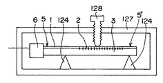
本発明に係る実施の形態19の導波路グレーティングデバイスは、図46に示すように、実施の形態18の導波路グレーティングデバイスにおいて、有機材料層119を取り除いて、その代わりにケース127内に窒素を封入して気密封止したものである。
具体的には、実施の形態18のケース117及び応力調整用スクリュー118に代えて、気密封止が可能なケース127及び応力調整用スクリュー128を用いて構成した。
尚、実施の形態19の導波路グレーティングデバイスにおいて、基板支持部124は、実施の形態18の基板支持部114と同様に構成した。
【0151】
実施の形態19において、基板3は、基板3の導波路グレーティング及び導波路が形成された面とは反対側の面が基板支持部124に接するように設けられ、応力調整用スクリュー128及び基板支持部124の熱膨張係数はケース127の熱膨張係数に比較して大きくなるように設定して、導波路グレーティング2の反射中心波長の温度による変化を補償している。
【0152】
以上のように構成された実施の形態19の導波路グレーティングデバイス(合分波器)は、応力調整用スクリュー128をしめこむ(下に移動させて基板が撓む方向に力を加える)ことにより、反射中心波長を低波長側に調整できる。
また、応力調整用スクリュー128及び基板支持部124とケース127との間の熱膨張の差により反射中心波長の温度による変化を補償することができる。
【0153】
次に、実施の形態19の導波路グレーティングデバイスの具体例について説明する。尚、本発明は以下の具体例に限定されるものではない。
本具体例では、横50mm、高さ20mm、奥行き20mmのインバール(熱膨張係数:1×10⁻⁶)製のケース127と、それぞれアルミニウム(熱膨張係数:24×10-6)からなる応力調整用スクリュー128及び基板支持部124、目標反射中心波長が1545.0nmの合分波器を作製した。
【0154】
本具体例において、応力印加前の導波路グレーティング2aの室温での反射中心波長は1545.2nmであり、所望の反射中心波長1545.0nmに対して0.2nmだけ大きかった。
そこで、図13の光学系において恒温槽14の温度を25℃とし、反射中心波長を観測しながら応力調整用スクリュー128を回転させて、反射中心波長を1545.0nmに調整した。
次に、恒温槽14の温度を変えながら反射中心波長を観測した。
その結果、温度に対する反射中心波長の変化率は10℃〜80℃において0.002nm/℃であり、従来と比較して1/5に低減された。
【0155】
また、本実施の形態19の導波路グレーティングデバイスでは、気密封止により基板3の機械的強度の劣化を防止し、信頼性を向上させている。
上述の本実施の形態19の具体例に係るサンプルを10個作製して、10℃〜80℃、90%RH温湿度サイクル試験を500サイクル行った結果、故障したサンプルは0個であった。
これに対して、気密封止をしない場合、同様な試験を行った結果では、サンプル10個中5個がサンプル表面にひび割れが発生した。この結果から防湿コート部により信頼性が向上することが確認できた。
【0156】
【発明の効果】
以上詳細に説明したように、本発明に係る導波路グレーティングデバイスは、上記基板支持体もしくは基板押圧手段、又は上記基板支持体及び上記基板押圧手段の両方が、温度の変化に対応して変化する該導波路グレーティングの反射中心波長の変化を打ち消す熱膨張係数を有し、上記基板押圧手段は、それぞれ基板に接する第1と第2の先端表面を有し、かつ該第1と第2の先端表面が上記導波路グレーティングを跨ぐように設けられた荷重分割部を先端部に有ているので、簡単な構成で温度補償できる。
【0157】
また、本発明に係る導波路グレーティングデバイスにおいて、上記基板支持体の先端表面を上記基板に平行な一直線を軸として曲率を有する円弧形状とすることにより、荷重の集中をより緩和することができるので、基板の破壊を防止でき、信頼性をより高くできる。
【0158】
また、本発明に係る導波路グレーティングデバイスでは、上記基板押圧手段の先端部に、それぞれ基板に接する第1と第2の先端表面を有し、かつ該第1と第2の先端表面が上記導波路グレーティングを跨ぐように設けられた荷重分割部を設けるようにしているので、荷重に対して基板の導波路グレーティングが形成された部分に生じる応力をほぼ均一に発生させることができ、応力の不均一により生じる特性の劣化を防止できる。
【0159】
さらに、本発明に係る導波路グレーティングデバイスでは、上記導波路グレーティングが形成された基板の表面に有機材料層を形成することにより信頼性をより向上させることができる。
【0160】
また、本発明に係る導波路グレーティングデバイスでは、上記防湿コートに代えて、上記ケース内に上記基板を気密封止するようにしても、信頼性を向上させることができる。
【図面の簡単な説明】
【図1】 本発明の原理を説明するための模式図である。
【図2】 導波路グレーティングにおける応力と反射中心波長の関係を示すグラフであって、(a)は導波路が形成された面が窪むように湾曲させた場合を示し、(b)は導波路が形成された面の反対側の面が窪むように湾曲させた場合を示す。
【図3】 温度補償しない場合の温度に対する反射中心波長を示すグラフである。
【図4】 温度補償した場合の温度に対する反射中心波長を示すグラフである。
【図5】 本発明に係る実施の形態1の構成を模式的に示す図であって、(a)は上方から見た平面図であり、(b)は側面からみた側面図である。
【図6】 実施の形態において用いた光学測定系を示すブロック図である。
【図7】 図6の光学測定系を用いて反射中心波長を調整する様子を模式的に示すグラフである。
【図8】 実施の形態1において、基板支持部4と基板3及び応力調整スクリュー8と基板3とをそれぞれ接着した場合と接着しない場合とにおける、荷重に対する中心波長の変化を示すグラフである。
【図9】 実施の形態1において、基板支持部4と基板3及び応力調整スクリュー8と基板3とをそれぞれ接着することなく、荷重により固定した例を示す図である。
【図10】 実施の形態1において、荷重に対する中心波長のシフト量を示すグラフである。
【図11】 実施の形態1における、基板支持部4と基板3の固定方法の一例を示す図である。
【図12】 実施の形態1における、基板支持部4と基板3の固定方法の他の例を示す図である。
【図13】 導波路グレーティングデバイスの温度特性を測定する測定系を示すブロック図である。
【図14】 本発明に係る実施の形態4の構成を模式的に示すブロック図である。
【図15】 本発明に係る実施の形態5の構成を模式的に示す図であって、(a)は上方から見た平面図であり、(b)は側面からみた側面図である。
【図16】 実施の形態4において、電圧を変化させたときの反射中心波長を示すグラフである。
【図17】 実施の形態4の導波路グレーティングデバイスにおいて、各ポートから出力されるパルス光の波形を示す図である。
【図18】 幅に対する厚さの比を変化させたときの、電圧に対する反射中心波長を示すグラフである。
【図19】 本発明に係る実施の形態6の構成を模式的に示す図であって、(a)は上方から見た平面図であり、(b)は側面からみた側面図である。
【図20】 本発明に係る実施の形態7の分散補償器の機能を説明するための図である。
【図21】 本発明に係る実施の形態8の可変分散補償器の分散特性を変化させる構成を説明するための模式的なブロック図である。
【図22】 実施の形態8の可変分散補償器の反射中心波長の調整及び温度特性の調整方法を説明するための模式的なブロック図である。
【図23】 実施の形態8の動作を説明するための、温度に対する反射中心波長を示すグラフである。
【図24】 実施の形態8の動作を説明するための、分散に対する反射中心波長を示すグラフである。
【図25】 導波路グレーティングデバイスの1つである帯域通過フィルタの構成を模式的に示す図である。
【図26】 導波路グレーティングデバイスの1つである合分波回路の構成を模式的に示す図である。
【図27】 導波路グレーティングデバイスの1つである分散補償器の構成を模式的に示す図である。
【図28】 光ファイバを通過する前の光パルス波形(a)と、光ファイバを通過した後の光パルス波形(b)を示す図である。
【図29】 分散補償器の動作を説明するための、波長に対する群遅延を示すグラフ(a)と波長に対する分散を示すグラフ(b)である。
【図30】 図29とは異なる特性の分散補償器の動作を説明するための、波長に対する群遅延を示すグラフ(a)と波長に対する分散を示すグラフ(b)である。
【図31】 補償値を可変できる分散補償器の構成を模式的に示す図である。
【図32】 補償値を可変できる分散補償器の動作を説明するためのグラフである。
【図33】 本発明に係る実施の形態7の分散補償器の構成を示す側面図である。
【図34】 本発明に係る実施の形態9の構成を模式的に示す図であって、(a)は上方から見た平面図であり、(b)は側面からみた側面図である。
【図35】 本発明に係る実施の形態10の構成を模式的に示す側面図である。
【図36】 本発明に係る実施の形態11の構成を模式的に示す側面図である。
【図37】 本発明に係る実施の形態12の構成を模式的に示す側面図である。
【図38】 本発明に係る実施の形態13の構成を模式的に示す側面図である。
【図39】 本発明に係る実施の形態14の構成を模式的に示す側面図である。
【図40】 本発明に係る実施の形態15の構成を模式的に示す図であって、(a)は横方向から見た側面図であり、(b)は端面方向からみた側面図である。
【図41】 (a)は、基板を、一点で荷重した時と、本実施の形態15に示すように2点で荷重した時の基板3に生じる歪量の分布を示すグラフであり、(b)は、(a)の評価条件を示す図である。
【図42】 本発明に係る実施の形態15の変形例の構成を模式的に示す図であって、(a)は横方向から見た側面図であり、(b)は端面方向からみた側面図である。
【図43】 本発明に係る実施の形態16の構成を模式的に示す側面図である。
【図44】 本発明に係る実施の形態17の構成を模式的に示す側面図である。
【図45】 本発明に係る実施の形態18の構成を模式的に示す側面図である。
【図46】 本発明に係る実施の形態19の構成を模式的に示す側面図である。
【符号の説明】
1 光導波路、2,2a 導波路グレーティング、3 基板、4,104,114,124,204,304,604,704,804,904 基板支持部、5 3dBカプラ、6 ファイバコネクタ、7,107,117,127,207,407,507,607,707,807,907 ケース、8,108,118,128,208,308,408a,408b,508,608,708,808,908a,908b,908c,908d,908e 応力調整用スクリュー、9 広帯域光源、10 スペクトルアナライザ、11 アイソレータ、12 導波路グレーティングデバイス、14 恒温槽、16 温度検出手段、17 温度検出回路、18 比較器、19 基準電圧発生回路、20 応力調整用アクチュエータ、21 有機材料層、22 光ファイバ、23 分散補償器、24 温度印加手段、119 防湿コート、207a,207b 凹部、507a 調整スクリュー取り付け部、608a ブレード、708a,708b 荷重分割具。[0001]
BACKGROUND OF THE INVENTION
The present invention relates to a reflection center wavelength control method for a waveguide grating, a temperature dependency compensation method for the reflection center wavelength, and a waveguide grating device using the same.
[0002]
[Prior art]
In ultra-high-speed wavelength division multiplexing optical communication systems, an optical multiplexer / demultiplexer, a bandpass filter for multiplexing / demultiplexing wavelength multiplexed signals, or a dispersion compensator for compensating for dispersion of an optical fiber as a transmission medium are key devices. Improvement of the characteristics is an important issue.
In recent years, with the advancement of wavelength division multiplexing optical communication systems, the reflection center wavelength control technology of optical multiplexer / demultiplexers, bandpass filters, or dispersion compensators that synthesize / demultiplex wavelength multiplexed signals is improved, or the temperature of the reflection center wavelength. The need to improve properties has increased.
[0003]
FIG. 25 shows an example of a conventional band pass filter using a waveguide grating. The waveguide grating used here has a function of reflecting light of a specific wavelength, and the reflection center wavelength λc is defined by the following equation (1). Where neffIs the effective refractive index of the waveguide grating, and Λ is the period of the waveguide grating.
[0004]
λc / neff= 2Λ Equation (1)
[0005]
In the bandpass filter shown in FIG. 25, the light input from the port P1 is branched into two by the 3
[0006]
FIG. 26 shows an example of a multiplexing / demultiplexing circuit using a waveguide grating. In the conventional multiplexing / demultiplexing circuit of FIG. 26, for example, when signals of various different wavelengths (λ1, λ2, λ3,...) Are incident from the port P1, only signal light of a specific wavelength (FIG. Then, λ1) is reflected by the
[0007]
FIG. 27 shows an example of a dispersion compensator using a waveguide grating. In optical communication, an optical fiber serving as an optical signal transmission medium has a dispersion in which the refractive index varies depending on the wavelength. Therefore, the speed of propagation through the transmission line differs depending on the wavelength of light, and the group delay amount varies depending on the wavelength. . Since the optical pulse signal has a spread in the wavelength component, if the signal propagates for several tens of kilometers due to the group delay difference depending on the wavelength, the signal spreads as shown in FIG. 28 ((a) in FIG. (B) shows the waveform after propagation. Therefore, ultra-high-speed optical communication requires a technique for compensating for the dispersion of the optical fiber.
[0008]
The relationship between the wavelength and the group delay when propagating through the optical fiber is as shown in FIG. 29A, and the dispersion expressed by the differentiation is shown as in FIG. 29B. Therefore, in order to compensate for this, devices having group delay and dispersion as shown in FIGS. 30A and 30B are necessary, which can be realized by the dispersion compensator shown in FIG. The waveguide grating 102 of this dispersion compensator is formed such that its period becomes longer as the distance from the input port side increases. By forming with the period changed in this way, the reflection position differs depending on the wavelength of the light, and the group delay is inclined as shown in FIG. That is, the dispersion becomes a positive constant value as shown in FIG. 30B, and the dispersion value can be compensated because the sign of the dispersion value of the optical fiber is reversed.
[0009]
FIG. 31 shows an example of a tunable dispersion compensator using a waveguide grating. The dispersion value required for the dispersion compensator (dispersion value to be compensated) varies depending on the length of the optical fiber used as the transmission path, the usage condition, and the like. Therefore, a dispersion compensator with a fixed dispersion value is used. In this case, a plurality of dispersion compensators having different dispersion values to be compensated are prepared and inserted, and the optimum one is selected. On the other hand, the variable dispersion compensator of FIG. 31 can finely adjust the dispersion value, so that the problem that trial and error for optimization is required can be solved. That is, in the tunable dispersion compensator shown in FIG. 31, heat is applied to the optical waveguide by the temperature applying means 24a and 24b. At this time, a heat gradient is generated in the waveguide grating by setting the amounts of heat generated by the temperature applying unit 24a and the temperature applying unit 24b to different values.
[0010]
Equivalent refractive index n of waveguide gratingeffIs a function of temperature, the thermal gradient generated when different heat is applied by the temperature applying means 24a and 24b is equivalent to the equivalent refractive index n of the optical waveguide.effIs inclined with respect to the longitudinal direction of the waveguide. In this way, the reflection center wavelength is n as shown in the equation (1).effTherefore, the reflection center wavelength changes depending on the position in the longitudinal direction of the waveguide grating. Therefore, the thermal gradient produces the same effect as a so-called chirped grating, and the distance to the reflection point differs according to the wavelength, thereby causing dispersion. In this way, the relationship between the temperature gradient, group delay, and dispersion can be as shown in FIGS. 32A, 32B, and 32C, and the dispersion value can be adjusted by changing the temperature gradient by the temperature application means.
[0011]
Next, a method for manufacturing a waveguide grating used in the above optical device will be described. As a typical method for producing a waveguide grating, there is a method using a light-induced refractive index change. The photoinduced refractive index change is a phenomenon in which the refractive index changes when ultraviolet light is irradiated onto a silica-based waveguide doped with germanium. Specifically, when interference fringes are formed by causing two ultraviolet lights to interfere with each other on the waveguide, a refractive index change corresponding to the period of the interference fringes occurs, and a waveguide grating is produced. The change in refractive index due to this is as small as about 0.001, but the period of the grating is as small as about 500 nm. Therefore, if the length is about 1 cm, a waveguide grating with about 20000 periods can be manufactured. It is possible to easily obtain a reflectance of approximately 100% at the reflection center wavelength.
[0012]
In the waveguide grating manufactured in this way, there is a manufacturing variation in the grating period, and therefore there is a certain variation in the reflection center wavelength of the grating. Also, in the production of a waveguide grating, if the ultraviolet light intensity or irradiation time is increased, or if the waveguide grating is produced tilted with respect to the direction perpendicular to the light traveling direction of the waveguide due to conditions such as setting, the reflection center The wavelength increases. Therefore, it is necessary to adjust the reflection center wavelength. Conventionally, after the waveguide grating is manufactured, the reflection center wavelength is measured. If the reflection center wavelength is different from the desired reflection center wavelength, ultraviolet light is further applied to the waveguide grating. The reflection center wavelength has been adjusted using an irradiation method (Japanese Patent Laid-Open No. 9-288205) or a heat treatment method (Japanese Patent Laid-Open No. 10-339821).
[0013]
In addition, the effective refractive index n of the waveguide using quartz-based materialeffChanges with temperature, and accordingly, the reflection center wavelength λc also changes as shown in FIG. In general, a grating fabricated on a quartz-based waveguide has a refractive index that changes at a rate of 0.01 nm / ° C. Therefore, the bandpass filter, multiplexer / demultiplexer, and dispersion compensator reflect with a change in temperature. It is necessary to take measures so that the center wavelength does not change. Since the problem that the reflection center wavelength changes due to this temperature change is caused by the temperature characteristics of the material itself, conventionally, temperature control is performed using a Peltier element, etc. A change in the reflection center wavelength is prevented by a method such as applying an optical medium having a temperature coefficient opposite to the rate on the waveguide (Japanese Patent Laid-Open No. 10-186167). At the 1999 IEICE General Conference, Arai et al. Titled “Temperature Characteristic Compensation of Waveguide Type Add / Drop Filter” (C-3-98) compared with a substrate on which a waveguide is formed. Techniques such as bonding a metal plate having a large thermal expansion coefficient to a substrate have been proposed.
[0014]
[Problems to be solved by the invention]
However, the method of re-irradiating the waveguide grating with ultraviolet light or the method of performing the heat treatment has a problem that adjustment takes time and cannot be manufactured at low cost.
In addition, regarding the structure that improves the temperature characteristics (decreases the change in the reflection center wavelength due to the temperature change), the structure is temperature controlled using a Peltier element or the like, and has a temperature coefficient opposite in sign to the refractive index of the waveguide. Both the structure in which the optical medium is deposited on the waveguide and the structure in which a metal plate having a larger thermal expansion coefficient than that of the substrate is bonded to the substrate have a problem that the structure is complicated and takes time to manufacture. there were.
[0015]
Accordingly, a first object of the present invention is to provide a waveguide grating device that can be easily controlled after its fabrication, compared to the conventional example.
A second object of the present invention is to provide a waveguide grating device that can reduce the change in the reflection center wavelength due to a change in temperature.
It is a third object of the present invention to provide a method for adjusting the reflection center wavelength of a waveguide grating that can easily adjust the reflection center wavelength after fabrication.
[0016]
[Means for Solving the Problems]
In order to achieve the above object, according to the present inventionGuidanceThe waveguide grating device includes a substrate having a waveguide grating having a Bragg wavelength, an optical waveguide connected to the waveguide grating, a case, and the substrate in contact with a first main surface of the substrate.UpA substrate support that is supported in the case, and is provided in the case, is in contact with the second main surface of the substrate opposite to the first main surface, and is movable in a direction perpendicular to the substrate. Or a fixed substrate pressing means,
The substrate is bent and fixed by the substrate pressing means.,
The substrate support or the substrate pressing means, or both the substrate support and the substrate pressing means have a thermal expansion coefficient that cancels the change in the reflection center wavelength of the waveguide grating that changes in response to a change in temperature.And
The substrate pressing means has first and second tip surfaces in contact with the substrate, respectively, and a load dividing portion provided so that the first and second tip surfaces straddle the waveguide grating. HaveIt is characterized by doing.
By configuring as described above, temperature compensation can be performed with a simple configuration.
[0017]
Further, according to the present inventionGuidanceIn the waveguide grating device, it is preferable that the tip surface of the substrate support is in linear contact with the substrate in order to reduce the concentration of load.
[0018]
Further, according to the present inventionGuidanceIn the waveguide grating device, the substrate support has an arc-shaped tip surface having a curvature with a straight line parallel to the substrate as an axis in order to reduce load concentration, and the tip surface is linear with the substrate. It is more preferable that the contact is made.
[0019]
Further, according to the present inventionGuidanceIn the waveguide grating device, the tip of the substrate pressing means has first and second tip surfaces in contact with the substrate, respectively, and the first and second tip surfaces are provided so as to straddle the waveguide grating. So as to provideHave.ThisThe stress generated in the portion of the substrate where the waveguide grating is formed with respect to the load can be generated almost uniformly.
[0020]
Furthermore, according to the present inventionGuidanceIn the waveguide grating device, the surface of the substrate on which the waveguide grating is formed or the surface on the opposite side is preferably coated with an organic material.
[0021]
Further, according to the present inventionGuidanceIn the waveguide grating device, the substrate may be hermetically sealed in the case instead of the coating with the organic material.
[0022]
DETAILED DESCRIPTION OF THE INVENTION
Embodiments according to the present invention will be described below with reference to the drawings.
First, before describing individual embodiments, the principle of the present invention will be described with reference to FIGS. In the following description, 1 is an optical waveguide, 2 is a waveguide grating, 3 is a substrate, and 4 is a substrate support.
As shown in FIG. 1 (a), a
[0023]
FIGS. 2A and 2B show the relationship between the reflection center wavelength and the stress when stress is applied in the directions shown in FIGS. In this way, since the grating period Λ can be shortened or extended depending on how stress is applied, it is possible to arbitrarily adjust the reflection center wavelength. Further, as the ratio t1 / L1 between the distance L1 between the
[0024]
Further, when the temperature changes, the effective refractive index of the waveguide grating 2 changes, and the change of the reflection center wavelength expressed by the equation (1) with the temperature is as shown in FIG. Accordingly, if the stress applied with the temperature change is appropriately changed to cancel the amount of change in the effective refractive index by the applied stress, the temperature characteristic is compensated and the reflection with respect to the temperature change is shown in FIG. The center wavelength can be prevented from changing.
Hereinafter, specific configurations regarding reflection center wavelength control (adjustment) and temperature characteristic compensation will be described with reference to the drawings.
[0025]
The waveguide
[0026]
That is, in the
[0027]
Hereafter, each component of the
For example, a pair of quartz-based waveguides doped with germanium are formed on the upper surface of the
The
[0028]
The
The
The
Here, the
The
The tip portion of the
[0029]
In the bandpass filter according to the first embodiment configured as described above, the light input from the port P1 is branched into two by the 3
[0030]
The bandpass filter according to the first embodiment has a structure in which an external force can be applied to the portion where the waveguide grating 2 is formed by the
When adjusting the reflection grating wavelength of the waveguide grating 2 by making it larger than that at the time of manufacture (before adjustment), the
[0031]
That is, in the configuration of the band pass filter of the first embodiment, when the reflection center wavelength of the waveguide grating 2 (center frequency of the pass band of the filter) is larger than a desired value, the surface on which the
When the reflection center wavelength of the waveguide grating 2 (the center frequency of the pass band of the filter) is smaller than a desired value, the surface on which the
For example, when a bandpass filter having a desired reflection center wavelength of 1553.0 nm is manufactured, when the reflection center wavelength of the bandpass filter before adjustment is 1552.5 nm, the surface on which the
[0032]
The reflection center wavelength of the band pass filter can be adjusted using the optical measurement system shown in FIG.
In this optical measurement system, for example, spontaneous emission light of an EDFA (Erbium-Doped Fiber Amplifier) can be used as the
An example of adjusting the reflection center wavelength to be larger than that at the time of manufacture is shown in FIG. That is, the reflection center wavelength can be shifted to the longer wavelength side by turning the
[0033]
Next, a method for supporting (fixing) the
As described above, in the first embodiment according to the present invention, the center wavelength of the waveguide grating 2 is changed by bending the
As a method of fixing the
[0034]
FIG. 8 is a graph showing changes in the center wavelength with respect to the load when the
Here, in this study, the
As is apparent from FIG. 8, when the
Therefore, in the first embodiment, as shown in FIG. 9, when the desired center wavelength is set, the substrate is bent and fixed so that a predetermined load is applied to the substrate.
In the first embodiment, if a load of 1000 g (1 kg) is applied, practically sufficient fixation is possible.
[0035]
FIG. 10 is a graph showing the shift amount of the center wavelength with respect to the load. When the thickness h of the
From FIG. 10, when a waveguide grating device having a desired center wavelength of 1555.0 nm is configured using a substrate having a thickness of 0.7 mm, the reflection center wavelength when no load is applied is 1555.7 nm. If the substrate is manufactured as described above, the
In FIG. 10, when the
[0036]
As described above, in the first embodiment, the
FIGS. 11A and 11B show an example (first example) in which a
Further, in the first example, the convex portion 3a is provided on the lower surface of the
By using the
[0037]
FIGS. 11C and 11D show another example (second example) using the
Even if it comprises using the board |
[0038]
12A and 12B show another example (third example) using the
Even if it comprises using the board |
[0039]
12 (c) and 12 (d) show that the
Even if it does as mentioned above, the board |
[0040]
The bandpass filter (waveguide grating device) of the first embodiment configured as described above can easily adjust the reflection center wavelength of the bandpass filter at the final stage of production (the stage where assembly is completed). In addition, the yield can be improved and the cost can be reduced.
[0041]
In the first embodiment, the
Further, by adopting the fixing structure shown in FIGS. 11 and 12, the
The fixing structure shown in FIGS. 11 and 12 can also be adopted in other embodiments described later, and in each of these embodiments, reliability such as vibration resistance can be improved.
[0042]
The waveguide grating device according to the second embodiment of the present invention uses a
[0043]
Specifically, for example, when the temperature characteristic is not compensated and the relationship between the temperature and the reflection center wavelength is as shown in FIG. 3, in order to compensate for this, the
[0044]
An example of the bandpass filter according to the second embodiment using polystyrene as the material for the
First, in this example, the reflection center wavelength before stress application was 1545.2 nm, while the desired reflection center wavelength at room temperature was 1545.0 nm. Thus, since it was larger by 0.2 nm than the desired reflection center wavelength, the substrate was set in the
[0045]
Next, the reflection center wavelength was observed while changing the temperature of the
[0046]
The bandpass filter according to the second embodiment configured as described above has the same effects as those of the first embodiment, and can further improve the temperature characteristics.
[0047]
The bandpass filter according to the third embodiment is the same as the bandpass filter according to the second embodiment, in which the
By setting in this way, when the reflection center wavelength of the waveguide grating 2 is smaller than a desired value, the reflection center wavelength can be increased by applying a bending stress with the
[0048]
In the configuration of the third embodiment, when the temperature characteristic is not compensated, the relationship between the temperature and the reflection center wavelength is as shown in FIG. In order to compensate for this, the material is selected so that the thermal expansion coefficient of the
[0049]
An example according to the third embodiment will be shown below.
In this example, the reflection center wavelength before stress application was 1556.2 nm, which was smaller by 0.3 nm than the desired reflection center wavelength 1556.5 nm at room temperature. Therefore, the
As described above, the bandpass filter according to the third embodiment has the same functions and effects as those of the second embodiment.
[0050]
As shown in FIG. 14, the bandpass filter of the fourth embodiment is different from the bandpass filter of the first embodiment in the following points, and other parts are configured in the same manner as in the first embodiment.
Differences from the first embodiment
(1) The
(2) Instead of the
(3) A
[0051]
The bandpass filter according to the fourth embodiment configured as described above has a structure in which stress can be applied to the waveguide grating 2 by the
[0052]
Next, the operation of the stress control circuit according to the fourth embodiment will be described.
The
[0053]
An example of the bandpass filter according to the fourth embodiment is shown below.
First, when the bandpass filter having the configuration shown in FIG. 14 was produced, the reflection center wavelength before stress application was 1554.7 nm, which was 0.4 nm smaller than the desired reflection center wavelength of 1555.1 nm. Therefore, the
Next, the reflection center wavelength was observed while changing the temperature of the
As described above, it was confirmed that the bandpass filter according to the fourth embodiment is effective for simple control of the reflection center wavelength and further improvement of temperature characteristics.
[0054]
FIG. 15A is a plan view and FIG. 15B is a cross-sectional view of the waveguide grating device according to the fifth embodiment of the present invention. The waveguide grating device of the fifth embodiment has a function as a wavelength variable type multiplexing / demultiplexing circuit.
In the fifth embodiment, first, a pair of
Here, the
A
[0055]
As described above, the
[0056]
In the fifth embodiment, as shown in FIG. 15A, the thickness of the substrate in the region where the waveguide grating 2 is formed is thinned by polishing so as to bend with a relatively small force. According to our study, when the length of the polished region in the longitudinal direction of the waveguide is L2 and the thickness of the substrate is t2, t2 and L2 are set so that the ratio satisfies t2 / L2 <0.5. When set, the
Further, as t2 / L2 becomes smaller, the gradient of the change of the reflection center wavelength with respect to the voltage becomes steeper as shown in FIG. However, if t2 is too thin, the mechanical strength cannot be maintained, and the
[0057]
In the wavelength tunable multiplexing / demultiplexing circuit which is the waveguide grating device 72 of the fifth embodiment configured as described above, signals having several kinds of wavelengths (λ1, λ2, λ3,...) Are transmitted from the port P1. Only signal light of a specific single wavelength corresponding to the expression (1) (λn) is reflected by the
[0058]
Here, in particular, the wavelength tunable multiplexing / demultiplexing circuit according to the fifth embodiment has a feature that the reflection center wavelength of the waveguide grating 2 can be arbitrarily selected by the
[0059]
As an example according to the fifth embodiment, the thickness t2 of the substrate in the region where the waveguide grating 2 is formed is 0.5 mm by polishing, and the ratio of the length L2 and t2 in the waveguide longitudinal direction of the polished region is as follows. Were prepared with t2 / L2 = 0.1.
In the fifth embodiment, the thickness of the
Conventionally, in the multiplexing / demultiplexing circuit using the waveguide grating formed on the substrate, only the reflection center wavelength is fixed, but the reflection center wavelength is changed by the actuator by the multiplexing / demultiplexing circuit of the fifth embodiment. A multiplexing / demultiplexing circuit that can be changed can be provided.
[0060]
As shown in FIG. 19, in the multiplexing / demultiplexing circuit of the sixth embodiment, an
[0061]
With this configuration, in the sixth embodiment, the thickness t2 of the substrate in the region where the waveguide grating exists can be reduced to 0.1 mm by polishing, and the length L2 of the polished region in the longitudinal direction of the waveguide The ratio of t2 could be t2 / L2 = 0.01. In order to make the substrate thin, a technique such as etching may be used instead of polishing. The
[0062]
Specifically, electromigration transfer carbazole and solubilized phthalocyanine were dissolved in a chloroform solution of PMMA, and the solution was dropped onto the surface of a waveguide set on a spin coater. A thin liquid layer is formed on the surface by centrifugal force, and a PMMA film is formed when the solution evaporates.
By doing so, in the multiplexing / demultiplexing circuit of the sixth embodiment, the reflection center wavelength can be made variable by applying stress by the
[0063]
As shown in FIG. 33, the waveguide grating device according to the seventh embodiment of the present invention is formed so that the grating period gradually increases in place of the waveguide grating 2 in the bandpass filter according to the first embodiment. The waveguide grating 2a is used and functions as a dispersion compensator. The configuration other than the above is the same as that of the first embodiment.
[0064]
In the dispersion compensator of the seventh embodiment, the light input from the port P1 is branched into two by the 3 dB coupler. The light having the reflection center wavelength λc of the waveguide grating 2a, that is, the signal light is reflected by the waveguide grating 2a, multiplexed again by the 3 dB coupler, and output from the port P2. Here, in particular, in the dispersion compensator, in order to obtain positive dispersion that cancels the negative dispersion caused by the optical fiber, the period of the waveguide grating is increased as the distance from the incident port side increases as described above. It has a dispersion characteristic corresponding to the change of the period.
[0065]
That is, since the optical pulse signal transmitted through the optical fiber has a wavelength spread slightly around λc, the optical pulse signal having a waveform as shown in FIG. After propagating for 10 kilometers, the fiber spreads in time as shown in FIG. 20B due to fiber dispersion. In order to correct this, the dispersion of the optical fiber has a negative value as shown in FIG. 29, whereas the dispersion of the dispersion compensator has a positive value. The grating period is increased as the distance from the incident port increases.
As a result, the optical pulse signal spread by propagating through the fiber of several tens of kilometers can be made into a waveform as shown in FIG. 20C by passing through the dispersion compensator, and the waveform before transmission through the optical fiber is obtained. It is corrected.
[0066]
The dispersion compensator of the seventh embodiment has a structure in which stress can be applied to the waveguide grating 2 by the
When the temperature characteristic is not compensated, the relationship between the temperature and the reflection center wavelength is as shown in FIG. 3. To compensate for this, the thermal expansion coefficients of the
[0067]
As a specific example of the seventh embodiment, aluminum is used for the
What was produced was 1.0 nm larger than the desired reflection center wavelength of 1551.0 m at room temperature, and the reflection center wavelength before applying stress was 1552.0 nm, so set the case with the waveguide surface facing the screw. did. In the optical measurement system of FIG. 13, the temperature of the
[0068]
Conventionally, it has been difficult to produce a dispersion compensator having a predetermined reflection center wavelength, but the reflection center wavelength of the dispersion compensator once produced by the dispersion compensator of the seventh embodiment can be adjusted very simply. Thus, the manufacturing yield can be improved and the cost can be reduced. Furthermore, it was confirmed that the present invention is effective in improving temperature characteristics.
[0069]
The waveguide grating device according to the eighth embodiment of the present invention is a tunable dispersion compensator, and FIG. 21 is a schematic block diagram for explaining a configuration for changing the dispersion characteristics of the tunable dispersion compensator. FIG. 22 is a schematic block diagram for explaining the method of adjusting the reflection center wavelength and the temperature characteristic of the tunable dispersion compensator.
The variable dispersion compensator of the eighth embodiment is
(1) A temperature application means 24 for forming a thermal gradient in the waveguide grating 2 provided on both sides of the waveguide grating 2 shown in FIG. 21, a
(2) In place of the
(3) A
[0070]
The variable dispersion compensator of the eighth embodiment has the same function as the variable dispersion compensator of the seventh embodiment and further has the following characteristics.
In other words, the dispersion value required for the dispersion compensator varies depending on the length of the fiber and the situation in which it is used. Conventionally, the dispersion compensator having several different dispersion values has been inserted, and the optimum one has been selected. As a result, the selection was very time-consuming. However, according to the tunable dispersion compensator of the eighth embodiment, it is possible to eliminate the trouble of selection.
[0071]
That is, in the tunable dispersion compensator of the eighth embodiment, the
Therefore, in the tunable dispersion compensator of the eighth embodiment, the necessary dispersion value is set by adjusting the thermal gradient applied to the waveguide grating 2 in accordance with the dispersion value depending on the length of the fiber, the usage condition, and the like. can do.
[0072]
The variable dispersion compensator of the present embodiment has a structure in which stress can be applied to the waveguide grating by an actuator, and the reflection center wavelength can be adjusted to a desired value.
Furthermore, the stress applied to the waveguide grating changes with the temperature change at the center of the grating portion, and the shift of the reflection center wavelength due to the temperature change when the dispersion value is changed is compensated.
When temperature characteristics are not compensated, the relationship between temperature and reflection center wavelength is as shown in FIG. In the stress control circuit for compensating for this, the temperature measured by the
[0073]
If the specific example of this
[0074]
Further, the change in the reflection center wavelength when the
As described above, conventionally, it has been difficult to manufacture a variable dispersion compensator having a predetermined reflection center wavelength, but the reflection center wavelength of a variable dispersion compensator once manufactured according to the configuration of the eighth embodiment is extremely low. Therefore, the manufacturing yield can be improved and the cost can be reduced.
Furthermore, it was confirmed that the present invention is effective for stabilizing the reflection center wavelength when the dispersion value is changed.
[0075]
As shown in FIG. 34, the waveguide grating device according to the ninth embodiment of the present invention is the same as the waveguide grading device (bandpass filter) according to the first embodiment. The configuration is the same as that of the first embodiment except that the configuration is made by using the
Here, in particular, in the waveguide grating device (bandpass filter) according to the ninth embodiment, the stress adjusting screw 108, the
[0076]
Specifically, in the waveguide grating device according to the ninth embodiment, the surface of the substrate on which the waveguide grating 2 is formed is configured to face the stress adjusting screw 108, and the stress adjusting screw 108 and the
[0077]
In the waveguide grating device according to the ninth embodiment configured as described above, the stress adjustment screw 108 and the
This can compensate for the temperature dependence of the reflection center wavelength of the waveguide grating 2 shown in FIG. 3 (the reflection center wavelength increases as the temperature rises), and even if the temperature changes as shown in FIG. The reflection center wavelength can be prevented from changing.
[0078]
Further, in the waveguide grating device (bandpass filter) according to the ninth embodiment, as in the first embodiment, the compression period is applied to the surface of the waveguide grating by inserting the stress adjusting screw 108 so that the grating period is shortened. Since the reflection center wavelength can be adjusted to the low wavelength side, the reflection center wavelength can be easily adjusted.
[0079]
As described above, the waveguide grating device according to the ninth embodiment of the present invention has the same operational effects as those of the first embodiment and can further improve the temperature characteristics.
[0080]
Next, a specific example of the waveguide grating device according to the ninth embodiment will be described.
The present invention is not limited to the following specific examples.
In this specific example, invar having a width of 50 mm, a height of 20 mm, and a depth of 20 mm (thermal expansion coefficient: 1 × 10⁻⁶)
[0090]
In this specific example, the reflection center wavelength before stress application at room temperature was 1545.2 nm, which was larger by 0.2 nm than the desired reflection center wavelength of 1545.0 nm. Therefore, in the optical system of FIG. 13, the temperature of the
As a result of observing the reflection center wavelength while changing the temperature of the
From this specific example, it was confirmed that the waveguide grating device according to the ninth embodiment can easily control the reflection center wavelength and can improve the temperature characteristics.
[0091]
In the waveguide grating device according to the ninth embodiment described above, the surface of the substrate on which the waveguide grating 2 is formed is configured to face the stress adjusting screw 108, so that the heat of the stress adjusting screw 108 and the
However, the present invention is not limited to this, and the surface opposite to the surface of the substrate on which the waveguide grating 2 is formed is configured to face the stress adjusting screw 108, so that the stress adjusting screw 108 and the substrate support portion are configured. The coefficient of
When the waveguide grating is formed so that the surface on which the waveguide grating is formed is set on the
[0092]
In the waveguide grating device according to the tenth embodiment of the present invention, as shown in FIG. 35, the waveguide grating 2 is formed in a case 207 having two
In the tenth embodiment, components similar to those in the first embodiment are denoted by the same reference numerals.
[0093]
In the waveguide grating device according to the tenth embodiment, the
The
The stress adjusting screw 208 is provided in contact with the surface of the
[0094]
Then, in the waveguide grating device according to the tenth embodiment, each material is selected so that the thermal expansion coefficients of the stress adjusting screw 108 and the
[0095]
In the waveguide device (bandpass filter) of the tenth embodiment, since the surface of the
In the tenth embodiment, since the thermal expansion coefficients of the stress adjustment screw 208 and the
[0096]
As described above, the waveguide grating device according to the tenth embodiment of the present invention can easily adjust the reflection center wavelength and has good temperature characteristics (the rate of change of the reflection center wavelength with respect to temperature), as in the first embodiment. Can be reduced).
Further, since the waveguide grating device of the tenth embodiment has a structure in which the
[0097]
Next, a specific example of the waveguide grating device according to the tenth embodiment will be described.
The present invention is not limited to the following specific examples.
In this specific example, aluminum having a width of 50 mm, a height of 15 mm, and a depth of 20 mm (thermal expansion coefficient: 24 × 10-6) Case 207 and Invar (thermal expansion coefficient: 1 × 10)-6A band pass filter having a target reflection center wavelength of 1545.0 nm was prepared using the stress adjusting screw 208 and the
[0098]
In this specific example, the reflection center wavelength before stress application at room temperature was 1544.8 nm, which was 0.2 nm smaller than the target value of 1545.0 nm. Therefore, in the optical measurement system of FIG. 13, the temperature of the
And as a result of observing the reflection center wavelength while changing the temperature of the
Further, since the
[0099]
As shown in FIG. 36, the waveguide grating device according to the eleventh embodiment of the present invention is the same as the waveguide grating device (bandpass filter) according to the ninth embodiment, instead of the
Here, in the eleventh embodiment, each of the
The arc shape having a curvature means that the tip portion of the
In the present invention, the tip portion of the
[0100]
In the eleventh embodiment, similarly to the ninth embodiment, since the surface of the substrate on which the waveguide grating 2 is formed is configured to face the
[0101]
The waveguide grating device according to the eleventh embodiment configured as described above has the same operational effects as the waveguide grating device according to the ninth embodiment, and can further improve the reliability of the device.
[0102]
Next, a specific example of the waveguide grating device according to the eleventh embodiment will be described. The present invention is not limited to the following specific examples.
In this specific example, invar having a width of 50 mm, a height of 20 mm, and a depth of 20 mm (thermal expansion coefficient: 1 × 10⁻⁶)
Here, each of the
[0103]
The reflection center wavelength of the
Therefore, in the optical system of FIG. 13, the temperature of the
Next, as a result of observing the reflection center wavelength while changing the temperature of the
In addition, as a result of performing a thermal cycle test from −20 ° C. to 80 ° C., when the tips of the substrate support part and the stress applying part were sharp, the tip was broken in about 500 cycles, whereas the tip was arcuate. In the case of this specific example, it was about 1000 cycles, and it was confirmed that the reliability was improved.
[0104]
As shown in FIG. 37, the waveguide grating device according to the twelfth embodiment of the present invention is different from the waveguide grating device according to the ninth embodiment in that two stresses are used instead of the stress adjusting screw 108 and the
[0105]
Here, in the twelfth embodiment, the two stress adjusting screws 408 a and 408 b are arranged so as to press the
[0106]
Next, a specific example of the waveguide grating device of the twelfth embodiment is shown.
The present invention is not limited to the following specific examples.
In this specific example, invar having a width of 50 mm, a height of 20 mm, and a depth of 20 mm (thermal expansion coefficient: 1 × 10⁻⁶)
[0107]
In this specific example, the reflection center wavelength before stress application at room temperature was 1545.2 nm, which was larger by 0.2 nm than the desired reflection center wavelength of 1545.0 nm. Therefore, in the optical system of FIG. 13, the temperature of the
As a result of observing the reflection center wavelength while changing the temperature of the
[0108]
Moreover, when the shape of the wavelength spectrum was observed together with the reflection center wavelength while changing the temperature of the
That is, when the stress adjusting screw is in contact with the waveguide grating 2 as in the ninth embodiment, the shape of the wavelength spectrum slightly changes when the temperature is changed from 10 ° C. to 80 ° C. This is because the waveguide grating 2 is directly subjected to stress by the stress adjusting screw 108, and the refractive index of the portion changes due to the photoelastic effect. On the other hand, the waveguide grating 2 is pressed by pressing the portions on both sides of the waveguide grating 2 with the two portions of the waveguide grating 2 away from each other by the two
[0109]
Embodiment 13 FIG.
A waveguide grating device (bandpass filter) according to the thirteenth embodiment of the present invention is different from the waveguide grating device according to the ninth embodiment in place of the stress adjusting screw 108 and the
[0110]
Here, in the waveguide grating device according to the thirteenth embodiment, the adjustment screw mounting portion 507a is provided so as to protrude from the upper surface of the
In the waveguide grating device of the thirteenth embodiment shown in FIG. 38, the surface of the substrate on which the waveguide grating 2 is formed is configured to face the
[0111]
Next, a specific example of the waveguide grating device according to the thirteenth embodiment will be described. The present invention is not limited to the following specific examples.
In this specific example, invar having a width of 50 mm, a height of 15 mm, and a depth of 20 mm (thermal expansion coefficient: 1 × 10⁻⁶)
In this specific example, the height of the portion of the
In addition, the
[0112]
In this specific example, the reflection center wavelength of the
Therefore, in the optical system of FIG. 13, the temperature of the
Next, the reflection center wavelength was observed while changing the temperature of the
As a result, the rate of change of the reflection center wavelength with respect to temperature was 0.002 nm / ° C. at 10 ° C. to 80 ° C., which was reduced to 1/5 compared to the conventional case.
[0113]
As described above, in the waveguide grating device according to the thirteenth embodiment, the thickness (15 mm) of the
[0114]
In the waveguide grating device (bandpass filter) according to the fourteenth embodiment of the present invention, as shown in FIG. 39, a
Specifically, a
Here, the tip portion of the substrate support portion 604 (tip portion in contact with the substrate 3) is formed in an arc shape centering on an axis parallel to the
The
[0115]
Further, the
In the fourteenth embodiment, the tip portion of the
In the fourteenth embodiment, the thermal expansion coefficients of the
[0116]
In the waveguide grating device of the fourteenth embodiment configured as described above, the reflection center wavelength is increased by tightening the stress adjusting screw 608 (moving it downward and applying a force in the direction in which the substrate bends). And the change of the reflection center wavelength due to the temperature can be compensated for by the difference in thermal expansion between the
Further, in the waveguide grating device according to the fourteenth embodiment, each tip portion (portion in contact with the substrate 3) of the
[0117]
Next, a specific example of the waveguide grating device according to the fourteenth embodiment will be described. The present invention is not limited to the following specific examples.
In this specific example, aluminum having a width of 50 mm, a height of 20 mm, and a depth of 20 mm (thermal expansion coefficient: 24 × 10-6)
[0118]
In this specific example, the reflection center wavelength of the
Therefore, in the optical system of FIG. 13, the temperature of the
Next, the reflection center wavelength was observed while changing the temperature of the
As a result, the rate of change of the reflection center wavelength with respect to temperature was 0.002 nm / ° C. at 10 ° C. to 80 ° C., which was reduced to 1/5 compared to the conventional case.
In addition, as a result of performing a thermal cycle test from −20 ° C. to 80 ° C., when the tips of the substrate support part and the stress applying part were sharp, the tip was broken in about 500 cycles, whereas the tip was arc In this specific example using the
[0119]
Embodiment 15 FIG.
In the waveguide grating device (dispersion compensator) according to the fifteenth embodiment of the present invention, a
Specifically, as shown in FIG. 40, a
In the waveguide grating device of FIG. 40, the
In addition, it is preferable that the front end portion of the
[0120]
In the fifteenth embodiment, the
[0121]
The waveguide grating device (dispersion compensator) of the fifteenth embodiment configured as described above performs the same dispersion compensation operation as the dispersion compensator of the seventh embodiment, and is the same as the dispersion compensator of the seventh embodiment. Or has the following excellent characteristics.
(1) In the waveguide grating device of the fifteenth embodiment, the reflection center wavelength is adjusted to be smaller by tightening the stress adjusting screw 708 (moving it downward and applying a force in the direction in which the substrate bends). it can.
(2) The change of the reflection center wavelength due to the temperature can be compensated by the difference in thermal expansion between the
(3) Deterioration of dispersion compensation characteristics (change in dispersion value) when the adjustment of (1) and the temperature compensation of (2) are performed are small compared to the dispersion compensator of the seventh embodiment.
[0122]
That is, as a dispersion compensator, it is desirable that the dispersion value is constant even when the temperature changes, but in order not to change the dispersion value, stress is uniformly applied to the waveguide grating, It is necessary that the refractive index does not change due to distortion.
However, when a load is directly applied to the portion where the waveguide grating 2a is formed by the stress adjusting screw, the compressive stress applied to the waveguide grating 2a becomes somewhat non-uniform, and the waveguide grating in the portion in contact with the stress adjusting screw further. Since the refractive index of 2a changes somewhat due to the photoelastic effect, the wavelength characteristics and dispersion characteristics change.
However, when stress is applied via the
For these reasons, the waveguide grating device (dispersion compensator) of the fifteenth embodiment can prevent the wavelength characteristics and the dispersion characteristics from deteriorating.
[0123]
As described above, according to the waveguide grating device of the fifteenth embodiment, it is possible to adjust the reflection center wavelength of the dispersion compensator once manufactured, and it is possible to improve the manufacturing yield and cost. Reduction is possible.
[0124]
Next, a specific example of the waveguide grating device according to the fifteenth embodiment will be described. The present invention is not limited to the following specific examples.
In this specific example, invar having a width of 50 mm, a height of 20 mm, and a depth of 20 mm (thermal expansion coefficient: 1 × 10⁻⁶)
[0125]
In this specific example, the reflection center wavelength of the waveguide grating 2a before stress application at room temperature was 1552.0 nm, which was larger by 1.0 nm than the desired reflection center wavelength of 1551.0 nm.
Therefore, in the optical system of FIG. 13, the temperature of the
Next, the reflection center wavelength was observed while changing the temperature of the
As a result, the rate of change of the reflection center wavelength with respect to temperature was 0.002 nm / ° C. at 10 ° C. to 80 ° C., which was reduced to 1/5 compared to the conventional case.
It was also confirmed that the degradation of the dispersion characteristics can be reduced in the above temperature range.
[0126]
FIG. 41A is a graph showing the distribution of the amount of strain generated in the
Specifically, as shown in FIG. 41B, the
Here, the simulation of FIG. 41B was performed using a finite element method. FIG. 41 (a) shows the amount of distortion at x = 0 mm to x = 10 mm, but it is clear from the symmetry of the sample that the same amount of distortion is shown at x = 10 mm to x = 20 mm. is there.
[0127]
As shown in FIG. 41 (a), in the two-point load, the strain amount shows a constant value between the two points to which the load is applied (x1 (x = 4 mm) to x3 (x = 16 mm)) With a one-point load, there is no range in which the amount of strain decreases monotonously toward the load point x2 and the strain amount becomes constant.
From the above, if the waveguide grating is formed between the two points to which the load is applied, in other words, the load is applied at two points so as to straddle the portion where the waveguide grating is formed. For example, the strain amount of the portion where the waveguide grating is formed by the load can be made constant, so that the dispersion characteristics can be prevented from deteriorating due to the load.
Although the dispersion compensator has been described in the fifteenth embodiment, a device similar to the fifteenth embodiment is applied by applying a two-point load to other waveguide grating devices such as a multiplexer / demultiplexer and a band pass filter. The center wavelength of the waveguide grating can be adjusted without degrading the characteristics.
[0128]
In the fifteenth embodiment described above, the
Further, when a load is applied as shown in FIG. 42, a load is not directly applied to a portion where the
[0129]
The waveguide grating device according to the sixteenth embodiment of the present invention is the same dispersion compensator as that of the fifteenth embodiment. In the waveguide grating device according to the fifteenth embodiment, a
Specifically, as shown in FIG. 43, a
In the waveguide grating device of FIG. 43, the
[0130]
In the sixteenth embodiment, the
[0131]
The waveguide grating device (dispersion compensator) of the sixteenth embodiment configured as described above performs the same dispersion compensation operation as the dispersion compensator of the fifteenth embodiment, and is the same as the dispersion compensator of the fifteenth embodiment. It has an excellent effect.
[0132]
Next, a specific example of the waveguide grating device according to the sixteenth embodiment will be described. The present invention is not limited to the following specific examples.
In this specific example, invar having a width of 50 mm, a height of 20 mm, and a depth of 20 mm (thermal expansion coefficient: 1 × 10⁻⁶)
[0133]
In this specific example, the reflection center wavelength of the waveguide grating 2a before stress application at room temperature was 1552.0 nm, which was larger by 1.0 nm than the desired reflection center wavelength of 1551.0 nm.
Therefore, in the optical system of FIG. 13, the temperature of the
Next, the reflection center wavelength was observed while changing the temperature of the
As a result, the rate of change of the reflection center wavelength with respect to temperature was 0.002 nm / ° C. at 10 ° C. to 80 ° C., which was reduced to 1/5 compared to the conventional case.
Further, in the above temperature range, it was confirmed that the degradation of the dispersion characteristics can be reduced as in the fifteenth embodiment.
In the above-described sixteenth embodiment, the dispersion compensator has been described as an example. However, the present invention is not limited to this, and can be applied to other waveguide grating devices such as a multiplexer / demultiplexer and a bandpass filter. can do.
[0134]
The waveguide grating device according to the seventeenth embodiment of the present invention is a multiplexer / demultiplexer, and 3
In the waveguide grating device (multiplexer / demultiplexer) of the seventeenth embodiment, the
[0135]
More specifically, the
A
[0136]
The waveguide grating device (multiplexer / demultiplexer) of the seventeenth embodiment configured as described above is guided when signals of several wavelengths (λ1, λ2, λ3,...) Are incident from the port P1. Corresponding to the period of the
[0137]
In the multiplexer / demultiplexer of the seventeenth embodiment configured as described above, the stress generated in the portion where the waveguide grating 2 is formed is changed by the five
In the seventeenth embodiment, the thermal expansion coefficient of the
[0138]
As described above, in the waveguide grating device according to the seventeenth embodiment, the temperature of the reflection center wavelength is compensated by compressive stress when the temperature is high, and the temperature of the reflection center wavelength is compensated by tensile stress when the temperature is low. Therefore, temperature compensation can be performed in a wide temperature range.
[0139]
Next, a specific example of the waveguide grating device according to the seventeenth embodiment will be described. The present invention is not limited to the following specific examples.
In this specific example, the
The
[0140]
In this specific example, the reflection center wavelength of the
Accordingly, in the optical system of FIG. 13, the temperature of the
When the reflection center wavelength of the waveguide grating 2 is larger than the target reflection center wavelength, the
[0141]
Next, the reflection center wavelength was observed while changing the temperature of the
As a result, the rate of change of the reflection center wavelength with respect to temperature was 0.002 nm / ° C. at −40 ° C. to 80 ° C., which was reduced to 1/5 compared with the conventional case.
As described above, it can be confirmed that the waveguide grating device according to the seventeenth embodiment is effective for simple control of the reflection center wavelength and for improving temperature characteristics over a wider range compared to the other embodiments. It was.
[0142]
In the above seventeenth embodiment, the multiplexer / demultiplexer has been described as an example, but the present invention can also be applied to other waveguide grating devices such as a dispersion compensator and a band pass filter.
[0143]
As shown in FIG. 45, the waveguide grating device according to the eighteenth embodiment of the present invention is a multiplexer / demultiplexer as in the seventeenth embodiment, and the
Here, in the waveguide grating device according to the eighteenth embodiment, the
In addition, an
The moisture-proof coat may be formed so as to cover the
[0144]
In the eighteenth embodiment, the
Specifically, electromigration transfer type carbazole and solubilized phthalocyanine are dissolved in a chloroform solution of PMMA, and the solution is dropped on the surface of the
[0145]
In the eighteenth embodiment, the
[0146]
In the waveguide grating device (multiplexer / demultiplexer) according to the eighteenth embodiment configured as described above, the
Further, the change in the reflection center wavelength due to the temperature can be compensated by the difference in thermal expansion between the
[0147]
Next, a specific example of the waveguide grating device according to the eighteenth embodiment will be described. The present invention is not limited to the following specific examples.
In this specific example, invar having a width of 50 mm, a height of 20 mm, and a depth of 20 mm (thermal expansion coefficient: 1 × 10⁻⁶)
[0148]
In this specific example, the reflection center wavelength of the waveguide grating 2a before stress application at room temperature was 1545.2 nm, which was 0.2 nm larger than the desired reflection center wavelength of 1545.0 nm.
Therefore, in the optical system of FIG. 13, the temperature of the
Next, the reflection center wavelength was observed while changing the temperature of the
As a result, the rate of change of the reflection center wavelength with respect to temperature was 0.002 nm / ° C. at 10 ° C. to 80 ° C., which was reduced to 1/5 compared to the conventional case.
[0149]
Moreover, since the waveguide grating device of the eighteenth embodiment has the
That is, a quartz film or a silicon substrate which is a substrate for forming a waveguide deteriorates in a high-temperature and high-humidity atmosphere, and the mechanical strength is weakened.
However, since the
Ten samples according to the specific example of the above-described eighteenth embodiment described above were produced and subjected to 10 cycles of 10 ° C. to 80 ° C. and 90% RH temperature / humidity cycle. As a result, the number of failed samples was zero.
On the other hand, when there was no
[0150]
As shown in FIG. 46, the waveguide grating device according to the nineteenth embodiment of the present invention is the same as the waveguide grating device according to the eighteenth embodiment, except that the
Specifically, instead of the
In the waveguide grating device according to the nineteenth embodiment, the
[0151]
In the nineteenth embodiment, the
[0152]
In the waveguide grating device (multiplexer / demultiplexer) according to the nineteenth embodiment configured as described above, the
Further, the change in the reflection center wavelength due to the temperature can be compensated by the difference in thermal expansion between the
[0153]
Next, a specific example of the waveguide grating device according to the nineteenth embodiment will be described. The present invention is not limited to the following specific examples.
In this specific example, invar having a width of 50 mm, a height of 20 mm, and a depth of 20 mm (thermal expansion coefficient: 1 × 10⁻⁶)
[0154]
In this specific example, the reflection center wavelength of the waveguide grating 2a before stress application at room temperature was 1545.2 nm, which was 0.2 nm larger than the desired reflection center wavelength of 1545.0 nm.
Therefore, in the optical system of FIG. 13, the temperature of the
Next, the reflection center wavelength was observed while changing the temperature of the
As a result, the rate of change of the reflection center wavelength with respect to temperature was 0.002 nm / ° C. at 10 ° C. to 80 ° C., which was reduced to 1/5 compared to the conventional case.
[0155]
In the waveguide grating device according to the nineteenth embodiment, the mechanical strength of the
Ten samples according to the specific example of the above-described nineteenth embodiment were produced and subjected to 10 cycles of 10 ° C. to 80 ° C. and 90% RH temperature / humidity cycle. As a result, the number of failed samples was zero.
On the other hand, in the case of not performing hermetic sealing, as a result of performing the same test, 5 out of 10 samples were cracked on the sample surface. From this result, it was confirmed that the moisture-proof coat portion improved the reliability.
[0156]
【The invention's effect】
As explained in detail above, according to the present inventionGuidanceWaveguide grating devicesThe substrate support or the substrate pressing means, or both the substrate support and the substrate pressing means have a thermal expansion coefficient that cancels the change in the reflection center wavelength of the waveguide grating that changes in response to a change in temperature. The substrate pressing means has first and second tip surfaces in contact with the substrate, respectively, and a load dividing portion provided so that the first and second tip surfaces straddle the waveguide grating. Temperature compensation with a simple configuration.
[0157]
Further, according to the present inventionGuidanceIn the waveguide grating device, since the tip surface of the substrate support has an arc shape having a curvature with a straight line parallel to the substrate as an axis, the concentration of load can be more relaxed, so that the destruction of the substrate can be prevented. , Can be more reliable.
[0158]
Further, according to the present inventionGuidanceIn the waveguide grating device, the tip of the substrate pressing means has first and second tip surfaces in contact with the substrate, respectively, and the first and second tip surfaces are provided so as to straddle the waveguide grating. So as to provideBecauseThe stress generated in the portion of the substrate where the waveguide grating is formed can be generated almost uniformly with respect to the load.,It is possible to prevent deterioration of characteristics caused by uneven stress.
[0159]
Furthermore, according to the present inventionGuidanceIn the waveguide grating device, the reliability can be further improved by forming an organic material layer on the surface of the substrate on which the waveguide grating is formed.
[0160]
Further, according to the present inventionGuidanceIn the waveguide grating device, the reliability can be improved even if the substrate is hermetically sealed in the case instead of the moisture-proof coat.
[Brief description of the drawings]
FIG. 1 is a schematic diagram for explaining the principle of the present invention.
FIG. 2 is a graph showing the relationship between stress and reflection center wavelength in a waveguide grating, where (a) shows the case where the waveguide is formed so that the surface on which the waveguide is formed is depressed; The case where it curves so that the surface on the opposite side of the formed surface may become depressed is shown.
FIG. 3 is a graph showing a reflection center wavelength with respect to temperature when temperature compensation is not performed;
FIG. 4 is a graph showing a reflection center wavelength with respect to temperature when temperature compensation is performed.
5A and 5B are diagrams schematically showing the configuration of the first embodiment according to the present invention, where FIG. 5A is a plan view seen from above, and FIG. 5B is a side view seen from the side.
FIG. 6 is a block diagram showing an optical measurement system used in the embodiment.
7 is a graph schematically showing how the reflection center wavelength is adjusted using the optical measurement system of FIG. 6; FIG.
FIG. 8 is a graph showing changes in the center wavelength with respect to load when the
FIG. 9 is a diagram showing an example in which the
10 is a graph showing the shift amount of the center wavelength with respect to the load in the first embodiment. FIG.
FIG. 11 is a diagram showing an example of a method for fixing the
12 is a diagram showing another example of a method for fixing the
FIG. 13 is a block diagram showing a measurement system for measuring temperature characteristics of a waveguide grating device.
FIG. 14 is a block diagram schematically showing the configuration of the fourth embodiment according to the present invention.
FIGS. 15A and 15B are diagrams schematically showing a configuration of a fifth embodiment according to the present invention, in which FIG. 15A is a plan view seen from above, and FIG. 15B is a side view seen from the side;
FIG. 16 is a graph showing the reflection center wavelength when the voltage is changed in the fourth embodiment.
FIG. 17 is a diagram illustrating a waveform of pulsed light output from each port in the waveguide grating device according to the fourth embodiment.
FIG. 18 is a graph showing the reflection center wavelength with respect to voltage when the ratio of thickness to width is changed.
FIGS. 19A and 19B are diagrams schematically showing a configuration of a sixth embodiment according to the present invention, in which FIG. 19A is a plan view seen from above, and FIG. 19B is a side view seen from the side;
FIG. 20 is a diagram for explaining the function of the dispersion compensator according to the seventh embodiment of the present invention.
FIG. 21 is a schematic block diagram for explaining a configuration for changing dispersion characteristics of a tunable dispersion compensator according to an eighth embodiment of the present invention;
FIG. 22 is a schematic block diagram for explaining a reflection center wavelength adjustment and temperature characteristic adjustment method of the tunable dispersion compensator according to the eighth embodiment;
FIG. 23 is a graph showing the reflection center wavelength with respect to temperature for explaining the operation of the eighth embodiment.
FIG. 24 is a graph showing the reflection center wavelength with respect to dispersion for explaining the operation of the eighth embodiment.
FIG. 25 is a diagram schematically showing a configuration of a band-pass filter that is one of the waveguide grating devices.
FIG. 26 is a diagram schematically showing a configuration of an multiplexing / demultiplexing circuit that is one of the waveguide grating devices.
FIG. 27 is a diagram schematically showing a configuration of a dispersion compensator which is one of the waveguide grating devices.
FIG. 28 is a diagram showing an optical pulse waveform (a) before passing through the optical fiber and an optical pulse waveform (b) after passing through the optical fiber.
FIG. 29 is a graph (a) showing a group delay with respect to a wavelength and a graph (b) showing dispersion with respect to a wavelength, for explaining the operation of the dispersion compensator.
30 is a graph (a) showing group delay with respect to wavelength and a graph (b) showing dispersion with respect to wavelength for explaining the operation of the dispersion compensator having characteristics different from those in FIG.
FIG. 31 is a diagram schematically illustrating a configuration of a dispersion compensator that can vary a compensation value;
FIG. 32 is a graph for explaining the operation of the dispersion compensator that can vary the compensation value;
FIG. 33 is a side view showing the configuration of the dispersion compensator according to the seventh embodiment of the present invention.
34 is a diagram schematically showing a configuration of a ninth embodiment according to the present invention, where (a) is a plan view seen from above, and (b) is a side view seen from the side. FIG.
FIG. 35 is a side view schematically showing the configuration of the tenth embodiment according to the present invention.
FIG. 36 is a side view schematically showing a configuration of an eleventh embodiment according to the present invention.
FIG. 37 is a side view schematically showing the configuration of the twelfth embodiment according to the present invention.
FIG. 38 is a side view schematically showing the configuration of the thirteenth embodiment according to the present invention.
FIG. 39 is a side view schematically showing the configuration of the fourteenth embodiment according to the present invention.
40 is a diagram schematically showing a configuration of a fifteenth embodiment according to the present invention, where (a) is a side view seen from the lateral direction, and (b) is a side view seen from the end surface direction. FIG. .
FIG. 41 (a) is a graph showing a distribution of strain amount generated in the
42 is a diagram schematically showing a configuration of a modified example of the fifteenth embodiment according to the present invention, where (a) is a side view seen from the lateral direction, and (b) is a side view seen from the end surface direction. FIG. FIG.
FIG. 43 is a side view schematically showing a configuration of an
FIG. 44 is a side view schematically showing the configuration of the seventeenth embodiment according to the present invention.
FIG. 45 is a side view schematically showing the configuration of the eighteenth embodiment according to the present invention.
FIG. 46 is a side view schematically showing the configuration of the nineteenth embodiment according to the present invention.
[Explanation of symbols]
DESCRIPTION OF
Claims (4)
上記導波路グレーティングに接続された光導波路と、
ケースと、
上記基板の第1の主面に接して上記基板を上記ケース内で支持する基板支持体と、
上記ケース内に設けられ、上記第1の主面とは反対側の上記基板の第2の主面に接し、上記基板と直交する方向に移動可能、又は固定された基板押圧手段と、を備え、
上記基板押圧手段によって上記基板を撓ませて固定し、
上記基板支持体もしくは基板押圧手段、又は上記基板支持体及び上記基板押圧手段の両方が、温度の変化に対応して変化する該導波路グレーティングの反射中心波長の変化を打ち消す熱膨張係数を有し、
上記基板押圧手段は、それぞれ基板に接する第1と第2の先端表面を有し、かつ該第1と第2の先端表面が上記導波路グレーティングを跨ぐように設けられた荷重分割部を先端部に有することを特徴とする導波路グレーティングデバイス。A substrate having a waveguide grating having a Bragg wavelength;
An optical waveguide connected to the waveguide grating;
Case and
A substrate support for supporting in the upper Symbol case the substrate in contact with the first main surface of the substrate,
A substrate pressing means provided in the case, in contact with the second main surface of the substrate opposite to the first main surface, and movable or fixed in a direction perpendicular to the substrate. ,
The substrate is bent and fixed by the substrate pressing means ,
The substrate support or substrate pressing means, or both the substrate support and the substrate pressing means, have a thermal expansion coefficient for canceling the change of the reflection center wavelength of the waveguide grating changes in response to changes in temperature ,
The substrate pressing means has first and second tip surfaces in contact with the substrate, respectively, and a load dividing portion provided so that the first and second tip surfaces straddle the waveguide grating. waveguide grating devices, characterized in that the perforated on.
Priority Applications (2)
| Application Number | Priority Date | Filing Date | Title |
|---|---|---|---|
| JP2000206869A JP4585091B2 (en) | 1999-08-19 | 2000-07-07 | Waveguide grating device |
| US09/640,000 US6522809B1 (en) | 1999-08-19 | 2000-08-17 | Waveguide grating device and method of controlling Bragg wavelength of waveguide grating |
Applications Claiming Priority (5)
| Application Number | Priority Date | Filing Date | Title |
|---|---|---|---|
| JP23268899 | 1999-08-19 | ||
| JP11-232688 | 2000-01-26 | ||
| JP2000017022 | 2000-01-26 | ||
| JP2000-17022 | 2000-01-26 | ||
| JP2000206869A JP4585091B2 (en) | 1999-08-19 | 2000-07-07 | Waveguide grating device |
Publications (3)
| Publication Number | Publication Date |
|---|---|
| JP2001281476A JP2001281476A (en) | 2001-10-10 |
| JP2001281476A5 JP2001281476A5 (en) | 2006-12-14 |
| JP4585091B2 true JP4585091B2 (en) | 2010-11-24 |
Family
ID=27331906
Family Applications (1)
| Application Number | Title | Priority Date | Filing Date |
|---|---|---|---|
| JP2000206869A Expired - Fee Related JP4585091B2 (en) | 1999-08-19 | 2000-07-07 | Waveguide grating device |
Country Status (2)
| Country | Link |
|---|---|
| US (1) | US6522809B1 (en) |
| JP (1) | JP4585091B2 (en) |
Families Citing this family (32)
| Publication number | Priority date | Publication date | Assignee | Title |
|---|---|---|---|---|
| CN1392961A (en) * | 2000-10-13 | 2003-01-22 | 古河电气工业株式会社 | Array waveguide type diffraction grating and light transmitting centre wavelength correcting method |
| FR2822240B1 (en) * | 2001-03-16 | 2003-09-05 | Highwave Optical Tech | FIBER OPTIC ATHERMIC DEVICE COMPRISING AN INTEGRATED COMPONENT |
| US6987908B2 (en) * | 2001-08-24 | 2006-01-17 | T-Networks, Inc. | Grating dispersion compensator and method of manufacture |
| EP1298466A1 (en) * | 2001-09-26 | 2003-04-02 | Aston Photonic Technologies Ltd. | Compensation of optical dispersion |
| US7110624B2 (en) * | 2001-12-14 | 2006-09-19 | Evans & Sutherland Computer Corporation | Fiber optic mechanical/thermal tuner and isolator |
| JP2003215367A (en) * | 2002-01-25 | 2003-07-30 | Mitsubishi Electric Corp | Optical device |
| US6842567B2 (en) * | 2002-02-07 | 2005-01-11 | Teraxion Inc. | Power efficient assemblies for applying a temperature gradient to a refractive index grating |
| JP4028340B2 (en) * | 2002-10-01 | 2007-12-26 | 古河電気工業株式会社 | Temperature compensated optical fiber grating components |
| CA2418382A1 (en) * | 2003-02-04 | 2004-08-04 | Teraxion Inc. | Athermally-passive, adjustable, chromatic dispersion compensator using a linearly chirped fbg |
| US8792531B2 (en) * | 2003-02-25 | 2014-07-29 | Finisar Corporation | Optical beam steering for tunable laser applications |
| US20050018964A1 (en) * | 2003-07-24 | 2005-01-27 | Yu Chen | Compensation of Bragg wavelength shift in a grating assisted direct coupler |
| WO2006055736A1 (en) | 2004-11-16 | 2006-05-26 | Illumina, Inc. | And methods and apparatus for reading coded microbeads |
| EP2104930A2 (en) | 2006-12-12 | 2009-09-30 | Evans & Sutherland Computer Corporation | System and method for aligning rgb light in a single modulator projector |
| WO2008080171A1 (en) * | 2006-12-22 | 2008-07-03 | Finisar Corporation | Optical transmitter having a widely tunable directly modulated laser and periodic optical spectrum reshaping element |
| US7941057B2 (en) * | 2006-12-28 | 2011-05-10 | Finisar Corporation | Integral phase rule for reducing dispersion errors in an adiabatically chirped amplitude modulated signal |
| US8131157B2 (en) | 2007-01-22 | 2012-03-06 | Finisar Corporation | Method and apparatus for generating signals with increased dispersion tolerance using a directly modulated laser transmitter |
| WO2008097928A1 (en) * | 2007-02-02 | 2008-08-14 | Finisar Corporation | Temperature stabilizing packaging for optoelectronic components in a transmitter module |
| US8027593B2 (en) | 2007-02-08 | 2011-09-27 | Finisar Corporation | Slow chirp compensation for enhanced signal bandwidth and transmission performances in directly modulated lasers |
| US7991291B2 (en) * | 2007-02-08 | 2011-08-02 | Finisar Corporation | WDM PON based on DML |
| US7991297B2 (en) | 2007-04-06 | 2011-08-02 | Finisar Corporation | Chirped laser with passive filter element for differential phase shift keying generation |
| US8204386B2 (en) | 2007-04-06 | 2012-06-19 | Finisar Corporation | Chirped laser with passive filter element for differential phase shift keying generation |
| US7760777B2 (en) * | 2007-04-13 | 2010-07-20 | Finisar Corporation | DBR laser with improved thermal tuning efficiency |
| US8160455B2 (en) | 2008-01-22 | 2012-04-17 | Finisar Corporation | Method and apparatus for generating signals with increased dispersion tolerance using a directly modulated laser transmitter |
| US8260150B2 (en) | 2008-04-25 | 2012-09-04 | Finisar Corporation | Passive wave division multiplexed transmitter having a directly modulated laser array |
| US8358317B2 (en) | 2008-05-23 | 2013-01-22 | Evans & Sutherland Computer Corporation | System and method for displaying a planar image on a curved surface |
| US8702248B1 (en) | 2008-06-11 | 2014-04-22 | Evans & Sutherland Computer Corporation | Projection method for reducing interpixel gaps on a viewing surface |
| US8077378B1 (en) | 2008-11-12 | 2011-12-13 | Evans & Sutherland Computer Corporation | Calibration system and method for light modulation device |
| TW201040604A (en) * | 2009-05-05 | 2010-11-16 | Nat Kaohsiung University Of Applied Scienses | Fiber optic sensor device |
| US8199785B2 (en) * | 2009-06-30 | 2012-06-12 | Finisar Corporation | Thermal chirp compensation in a chirp managed laser |
| US9641826B1 (en) | 2011-10-06 | 2017-05-02 | Evans & Sutherland Computer Corporation | System and method for displaying distant 3-D stereo on a dome surface |
| US9239431B1 (en) * | 2011-11-29 | 2016-01-19 | Sandia Corporation | Athermalization of resonant optical devices via thermo-mechanical feedback |
| US9816941B2 (en) * | 2016-03-28 | 2017-11-14 | Saudi Arabian Oil Company | Systems and methods for constructing and testing composite photonic structures |
Citations (5)
| Publication number | Priority date | Publication date | Assignee | Title |
|---|---|---|---|---|
| JPS6249307A (en) * | 1985-06-12 | 1987-03-04 | エヌ・ベ−・フイリツプス・フル−イランペンフアブリケン | Magnetooptic waveguide device for propagation mode conversion of device |
| JPH05157640A (en) * | 1991-12-09 | 1993-06-25 | Matsushita Electric Ind Co Ltd | Optical waveguide type stress sensor |
| JPH0792400A (en) * | 1993-09-20 | 1995-04-07 | Sumitomo Electric Ind Ltd | Optical waveguide |
| JPH08101310A (en) * | 1994-09-30 | 1996-04-16 | Nippon Telegr & Teleph Corp <Ntt> | Reflection type fiber grating filter |
| JPH08235603A (en) * | 1995-02-24 | 1996-09-13 | Ricoh Co Ltd | Optical waveguide-type detection apparatus |
Family Cites Families (11)
| Publication number | Priority date | Publication date | Assignee | Title |
|---|---|---|---|---|
| US5042898A (en) | 1989-12-26 | 1991-08-27 | United Technologies Corporation | Incorporated Bragg filter temperature compensated optical waveguide device |
| JP2682367B2 (en) | 1993-02-16 | 1997-11-26 | コクヨ株式会社 | Adjuster device for furniture |
| JPH09288205A (en) | 1996-04-19 | 1997-11-04 | Fujikura Ltd | Production of optical waveguide grating |
| US5774619A (en) * | 1996-05-15 | 1998-06-30 | Hughes Electronics Corporation | Precision deformation mechanism and method |
| JPH10186167A (en) | 1996-12-20 | 1998-07-14 | Toshiba Corp | Optical filter |
| JPH10339821A (en) | 1997-06-09 | 1998-12-22 | Sumitomo Electric Ind Ltd | Manufacture of optical waveguide type grating |
| US5978539A (en) | 1997-10-03 | 1999-11-02 | Lucent Technologies Inc. | Optical device having a temperature independent spectral response using nonplanar geometric distortion of a substrate |
| CA2353567C (en) * | 1998-12-04 | 2007-11-20 | Cidra Corporation | Bragg grating pressure sensor |
| JP3331180B2 (en) * | 1998-12-18 | 2002-10-07 | 日本電信電話株式会社 | Temperature-independent planar optical device |
| JP2000206348A (en) * | 1999-01-13 | 2000-07-28 | Furukawa Electric Co Ltd:The | Compensation method of light transmission wavelength of optical waveguide circuit |
| US6144789A (en) * | 1999-05-25 | 2000-11-07 | Lucent Technologies Inc. | Temperature compensating device for fiber gratings and a package therefor |
-
2000
- 2000-07-07 JP JP2000206869A patent/JP4585091B2/en not_active Expired - Fee Related
- 2000-08-17 US US09/640,000 patent/US6522809B1/en not_active Expired - Fee Related
Patent Citations (5)
| Publication number | Priority date | Publication date | Assignee | Title |
|---|---|---|---|---|
| JPS6249307A (en) * | 1985-06-12 | 1987-03-04 | エヌ・ベ−・フイリツプス・フル−イランペンフアブリケン | Magnetooptic waveguide device for propagation mode conversion of device |
| JPH05157640A (en) * | 1991-12-09 | 1993-06-25 | Matsushita Electric Ind Co Ltd | Optical waveguide type stress sensor |
| JPH0792400A (en) * | 1993-09-20 | 1995-04-07 | Sumitomo Electric Ind Ltd | Optical waveguide |
| JPH08101310A (en) * | 1994-09-30 | 1996-04-16 | Nippon Telegr & Teleph Corp <Ntt> | Reflection type fiber grating filter |
| JPH08235603A (en) * | 1995-02-24 | 1996-09-13 | Ricoh Co Ltd | Optical waveguide-type detection apparatus |
Also Published As
| Publication number | Publication date |
|---|---|
| US6522809B1 (en) | 2003-02-18 |
| JP2001281476A (en) | 2001-10-10 |
Similar Documents
| Publication | Publication Date | Title |
|---|---|---|
| JP4585091B2 (en) | Waveguide grating device | |
| US7164478B2 (en) | Apparatus and methods for stabilization and control of fiber devices and fiber devices including the same | |
| ES2399294T3 (en) | Method and system for integrated DWDM transmitters | |
| US6031948A (en) | Fused-fiber multi-window wavelength division multiplexer using an unbalanced Mach-Zehnder interferometer and method of making same | |
| JP2000206348A (en) | Compensation method of light transmission wavelength of optical waveguide circuit | |
| WO2018036035A1 (en) | Athermal arrayed wavelength grating with temperature compensation and manufacturing method thereof | |
| US6269202B1 (en) | Highly temperature stable filter for fiberoptic applications and system for altering the wavelength or other characteristics of optical devices | |
| JPWO2002033462A1 (en) | Arrayed waveguide type diffraction grating and method of correcting center wavelength of light transmission thereof | |
| JP2002031729A (en) | Array waveguide diffraction grating type optical multiplexer/demultiprexer | |
| WO2001090803A2 (en) | Optical add/drop multiplexer | |
| US6735364B2 (en) | Arrayed waveguide grating optical multiplexer/demultiplexer and method for manufacturing the same | |
| US6850654B2 (en) | Passive thermal compensation of all-fiber Mach-Zehnder interferometer | |
| US7177499B2 (en) | Athermal package for fiber bragg gratings with compensation for non-linear thermal response | |
| US20030016928A1 (en) | Optical waveguide | |
| CA2342098C (en) | Optical filter device for temperature dependence control | |
| US20040161197A1 (en) | Adjustable chromatic dispersion compensator | |
| US6735365B2 (en) | Fused fiber interleaver | |
| US6498879B1 (en) | Polarization-independent, environmentally stable optical fiber narrow band multi-window wavelength division multiplexer based on biconical tapered fusion coupler technology | |
| JP3956805B2 (en) | Optical module | |
| JP4477263B2 (en) | Method of manufacturing arrayed waveguide grating optical multiplexer / demultiplexer | |
| WO2010018757A1 (en) | Light multiplexer | |
| CA2379404A1 (en) | Optical coupling device | |
| US20030086176A1 (en) | Sandwiched thin film optical filter | |
| MATSUURA | Development of 12.5/25 GHz Optical Interleaving Filter Module with Isolator Function | |
| US6987909B1 (en) | Optical systems and athermalized optical component apparatuses and methods for use therein |
Legal Events
| Date | Code | Title | Description |
|---|---|---|---|
| A521 | Written amendment |
Free format text: JAPANESE INTERMEDIATE CODE: A523 Effective date: 20061031 |
|
| A621 | Written request for application examination |
Free format text: JAPANESE INTERMEDIATE CODE: A621 Effective date: 20061031 |
|
| A977 | Report on retrieval |
Free format text: JAPANESE INTERMEDIATE CODE: A971007 Effective date: 20080108 |
|
| A131 | Notification of reasons for refusal |
Free format text: JAPANESE INTERMEDIATE CODE: A131 Effective date: 20080909 |
|
| A521 | Written amendment |
Free format text: JAPANESE INTERMEDIATE CODE: A523 Effective date: 20081027 |
|
| RD03 | Notification of appointment of power of attorney |
Free format text: JAPANESE INTERMEDIATE CODE: A7423 Effective date: 20081027 |
|
| A131 | Notification of reasons for refusal |
Free format text: JAPANESE INTERMEDIATE CODE: A131 Effective date: 20090908 |
|
| A521 | Written amendment |
Free format text: JAPANESE INTERMEDIATE CODE: A523 Effective date: 20091030 |
|
| TRDD | Decision of grant or rejection written | ||
| A01 | Written decision to grant a patent or to grant a registration (utility model) |
Free format text: JAPANESE INTERMEDIATE CODE: A01 Effective date: 20100831 |
|
| A01 | Written decision to grant a patent or to grant a registration (utility model) |
Free format text: JAPANESE INTERMEDIATE CODE: A01 |
|
| A61 | First payment of annual fees (during grant procedure) |
Free format text: JAPANESE INTERMEDIATE CODE: A61 Effective date: 20100903 |
|
| R150 | Certificate of patent or registration of utility model |
Free format text: JAPANESE INTERMEDIATE CODE: R150 |
|
| FPAY | Renewal fee payment (event date is renewal date of database) |
Free format text: PAYMENT UNTIL: 20130910 Year of fee payment: 3 |
|
| R250 | Receipt of annual fees |
Free format text: JAPANESE INTERMEDIATE CODE: R250 |
|
| LAPS | Cancellation because of no payment of annual fees |