JP4581011B2 - Electrical parts and manufacturing method - Google Patents
Electrical parts and manufacturing method Download PDFInfo
- Publication number
- JP4581011B2 JP4581011B2 JP2008282499A JP2008282499A JP4581011B2 JP 4581011 B2 JP4581011 B2 JP 4581011B2 JP 2008282499 A JP2008282499 A JP 2008282499A JP 2008282499 A JP2008282499 A JP 2008282499A JP 4581011 B2 JP4581011 B2 JP 4581011B2
- Authority
- JP
- Japan
- Prior art keywords
- film
- insulating
- cavity
- electrical component
- functional element
- Prior art date
- Legal status (The legal status is an assumption and is not a legal conclusion. Google has not performed a legal analysis and makes no representation as to the accuracy of the status listed.)
- Expired - Fee Related
Links
Images


Classifications
-
- B—PERFORMING OPERATIONS; TRANSPORTING
- B81—MICROSTRUCTURAL TECHNOLOGY
- B81B—MICROSTRUCTURAL DEVICES OR SYSTEMS, e.g. MICROMECHANICAL DEVICES
- B81B7/00—Microstructural systems; Auxiliary parts of microstructural devices or systems
- B81B7/0032—Packages or encapsulation
- B81B7/0035—Packages or encapsulation for maintaining a controlled atmosphere inside of the chamber containing the MEMS
- B81B7/0038—Packages or encapsulation for maintaining a controlled atmosphere inside of the chamber containing the MEMS using materials for controlling the level of pressure, contaminants or moisture inside of the package, e.g. getters
-
- H—ELECTRICITY
- H01—ELECTRIC ELEMENTS
- H01L—SEMICONDUCTOR DEVICES NOT COVERED BY CLASS H10
- H01L23/00—Details of semiconductor or other solid state devices
- H01L23/02—Containers; Seals
- H01L23/04—Containers; Seals characterised by the shape of the container or parts, e.g. caps, walls
- H01L23/053—Containers; Seals characterised by the shape of the container or parts, e.g. caps, walls the container being a hollow construction and having an insulating or insulated base as a mounting for the semiconductor body
- H01L23/055—Containers; Seals characterised by the shape of the container or parts, e.g. caps, walls the container being a hollow construction and having an insulating or insulated base as a mounting for the semiconductor body the leads having a passage through the base
-
- B—PERFORMING OPERATIONS; TRANSPORTING
- B81—MICROSTRUCTURAL TECHNOLOGY
- B81C—PROCESSES OR APPARATUS SPECIALLY ADAPTED FOR THE MANUFACTURE OR TREATMENT OF MICROSTRUCTURAL DEVICES OR SYSTEMS
- B81C1/00—Manufacture or treatment of devices or systems in or on a substrate
- B81C1/00436—Shaping materials, i.e. techniques for structuring the substrate or the layers on the substrate
- B81C1/00444—Surface micromachining, i.e. structuring layers on the substrate
- B81C1/00468—Releasing structures
- B81C1/00476—Releasing structures removing a sacrificial layer
-
- B—PERFORMING OPERATIONS; TRANSPORTING
- B81—MICROSTRUCTURAL TECHNOLOGY
- B81B—MICROSTRUCTURAL DEVICES OR SYSTEMS, e.g. MICROMECHANICAL DEVICES
- B81B2201/00—Specific applications of microelectromechanical systems
- B81B2201/02—Sensors
- B81B2201/0221—Variable capacitors
-
- B—PERFORMING OPERATIONS; TRANSPORTING
- B81—MICROSTRUCTURAL TECHNOLOGY
- B81B—MICROSTRUCTURAL DEVICES OR SYSTEMS, e.g. MICROMECHANICAL DEVICES
- B81B2203/00—Basic microelectromechanical structures
- B81B2203/04—Electrodes
Description
本発明は、例えば半導体集積回路に内蔵される電気部品とその製造方法に係わり、機械的に動作可能な構成を有するMEMS(Micro Electro Mechanical System)に関する。 The present invention relates to an electrical component incorporated in, for example, a semiconductor integrated circuit and a manufacturing method thereof, and relates to a micro electro mechanical system (MEMS) having a mechanically operable configuration.
MEMSは、可動部を有する機能素子であるため、可動部の動作空間としてのキャビティ(空洞)を必要とし、このキャビティは、外気の浸入を遮断して機能素子を保護するため、気密封止されている。 Since MEMS is a functional element having a movable part, it requires a cavity as an operating space of the movable part, and this cavity is hermetically sealed in order to protect the functional element by blocking intrusion of outside air. ing.
従来、気密封止は金属封止法、ハンダ封止法、ガラス封止法などのように、ガスが透過しない封止材を用いて行われていた。 Conventionally, hermetic sealing has been performed using a sealing material that does not transmit gas, such as a metal sealing method, a solder sealing method, and a glass sealing method.
然しながら、金属封止法やハンダ封止法は、機能素子や電気配線と封止金属との間に寄生容量が生じるため、機能素子の特性に影響を与える問題がある。 However, the metal sealing method and the solder sealing method have a problem of affecting the characteristics of the functional element because a parasitic capacitance is generated between the functional element or the electric wiring and the sealing metal.
ガラス封止法は、封止温度が300〜400℃と高いため、耐熱性の低い機能素子の気密封止には適さないという問題がある。 Since the glass sealing method has a high sealing temperature of 300 to 400 ° C., there is a problem that it is not suitable for hermetic sealing of functional elements having low heat resistance.
これに対して、基板上の犠牲膜をエッチングして形成されたキャビティ内に気密封止された機能素子が知られている。(例えば、特許文献1参照。)。 On the other hand, a functional element hermetically sealed in a cavity formed by etching a sacrificial film on a substrate is known. (For example, refer to Patent Document 1).
特許文献1に開示された機能素子は、シリコン基板上の機能素子が犠牲膜で覆われ、犠牲膜上に開口を有する耐エッチング膜が形成される。この開口を通して犠牲膜がエッチングされることにより犠牲膜によりキャビティが形成され、このキャビティ内に機能素子が収納される。この後、犠牲膜上にシリコン窒化膜が形成されて開口が封止されることにより、キャビティ内が気密封止される。
In the functional element disclosed in
然しながら、特許文献1に開示された技術において、シリコン窒化膜はSi基板に対して圧縮力が大きいため、キャビティを形成する耐エッチング膜の変形を引き起こし、キャビティを経時的に変形させる問題がある。
However, in the technique disclosed in
開口の封止に用いるシリコン窒化膜を薄くすれば、膜の応力も小さくなる。しかし、シリコン窒化膜を薄くした場合、開口からキャビティ内へシリコン窒化膜が落下することを防止し、且つ開口を封止するために、開口のサイズを十分小さくする必要がある。このため、小さい開口から犠牲膜を除去するために長時間を要し、また、エッチング不足により、キャビティ内に犠牲膜の残るという問題がある。
本発明は、信頼性の高い電位部品とその製造方法を提供しようとするものである。 The present invention seeks to provide a highly reliable potential component and a method for manufacturing the same.
本発明の電気部品の態様は、機能素子を有する基板と、前記基板とともに前記機能素子を収納する空洞を形成し、複数の貫通孔を有する絶縁性の第1の膜と、前記複数の貫通孔の上面を塞いで前記第1の膜上に形成され、前記第1の膜よりガス透過率の大きい絶縁性の第2の膜と、少なくとも前記第2の膜上に形成され、前記第2の膜よりガス透過率の小さい絶縁性の第3の膜と、前記第3の膜上に形成され、前記第3の膜より伸縮性の大きい絶縁性の第4の膜と、を具備することを特徴とする。
本発明の電気部品の製造方法は、基板上に機能素子を形成し、前記基板と複数の貫通孔を有する絶縁性の第1の膜とにより前記機能素子を収納する空洞を形成し、前記複数の貫通孔の上面を塞ぐため、前記第1の膜上に前記第1の膜よりガス透過率の大きい絶縁性の第2の膜を形成し、少なくとも前記第2の膜上に前記第2の膜よりガス透過率の小さい絶縁性の第3の膜を形成し、前記第3の膜上に前記第3の膜より伸縮性の大きい絶縁性の第4の膜を形成したことを特徴とする。
An aspect of the electrical component of the present invention includes: a substrate having a functional element; an insulating first film having a plurality of through holes that forms a cavity for housing the functional element together with the substrate; and the plurality of through holes An insulating second film having a higher gas permeability than the first film, and at least the second film, and is formed on the first film. An insulating third film having a gas permeability smaller than that of the film; and an insulating fourth film formed on the third film and having a higher elasticity than the third film. Features.
In the method for manufacturing an electrical component according to the present invention, a functional element is formed on a substrate, and a cavity for accommodating the functional element is formed by the substrate and an insulating first film having a plurality of through holes. In order to block the upper surface of the through-hole, an insulating second film having a higher gas permeability than the first film is formed on the first film, and at least the second film is formed on the second film. An insulating third film having a gas permeability smaller than that of the film is formed, and an insulating fourth film having a higher elasticity than the third film is formed on the third film. .
本発明によれば、信頼性の高い電気部品とその製造方法を提供できる。 ADVANTAGE OF THE INVENTION According to this invention, a reliable electrical component and its manufacturing method can be provided.
以下、本発明の実施の形態について、図面を参照して説明する。 Embodiments of the present invention will be described below with reference to the drawings.
(第1の実施例)
図1乃至図4を用いて、本発明の第1の実施例に係る電気部品について説明する。図1は電気部品を示す断面図、図2乃至図4は電気部品の製造工程の要部を順に示す断面図である。
(First embodiment)
The electrical component according to the first embodiment of the present invention will be described with reference to FIGS. FIG. 1 is a cross-sectional view showing an electrical component, and FIGS. 2 to 4 are cross-sectional views sequentially showing a main part of an electrical component manufacturing process.
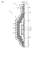
図1に示すように、本実施例の電気部品10は、機能素子11を有する基板12と、基板12とともに機能素子11を収納するキャビティ13を形成し、複数の貫通孔14aを有する絶縁性の第1の膜14と、複数の貫通孔14aの上面を塞いで第1の膜14上に形成され、第1の膜14よりガス透過率の大きい絶縁性の第2の膜15と、を具備している。
As shown in FIG. 1, the
更に、電気部品10は、第2の膜15上に形成され、第2の膜15よりガス透過率の小さい絶縁性の第3の膜16と、第3の膜16上に形成され、第3の膜16より伸縮性の大きい絶縁性の第4の膜17と、を具備している。
Further, the
基板12は、例えばシリコン基板であり、基板12上の絶縁膜18は、例えばシリコン酸化膜である。この絶縁膜18上に機能素子11が形成されている。機能素子11は、例えば静電駆動型のMEMS可変容量キャパシタである。
The
MEMS可変容量キャパシタは、例えばアルミニウムの第1電極11aと、第1電極11aに対向するアルミニウムの第2電極11bにより構成されている。この可変容量キャパシタは、第1電極11aと第2電極11bの間に電圧を印加すると、静電引力によって第1部電極11aと第2電極11bとの間の距離が変化することにより容量が変化する。
The MEMS variable capacitance capacitor includes, for example, an aluminum
キャビティ13は、機能素子11の動作空間を確保するための領域である。キャビティ13内は、乾燥雰囲気、または真空雰囲気に保たれている。このため、有害ガス、例えば水分によるアルミニウム製の第1および第2電極11a、11bの劣化が防止され、MEMS可変容量キャパシタの特性劣化が防止されている。本実施例では、電極材料としてアルミニウムを用いた例を示している。しかし、電気的信頼性の向上、動作回数の増加に伴って徐々に塑性変形を伴うクリープ現象を低減させるため、銅(Cu)を添加したアルミニウム合金を用いることが望ましい。
The
第1の膜14は、Si―O結合を主成分とするシリコン化合物、例えば厚さが1μm程度のシリコン酸化膜であり、機能素子11を外部から保護するためのキャップとしての無機膜である。
The
第1の膜14の複数の貫通孔(開口)14aは、後述するように機能素子11を形成した後、犠牲層をエッチングして除去し、キャビティ13を形成するためのものである。すなわち、犠牲層は、貫通孔14aを通してエッチングされる。
The plurality of through holes (openings) 14 a of the
第2の膜15は、有機膜、例えば炭素を主成分とする紫外線硬化型樹脂であり、具体的にはプレポリマー、モノマー、光重合開始剤、添加剤などからなる樹脂膜である。この第2の膜15は、後述するように、キャビティ13を形成した後、貫通孔14aの上面を塞いで第1の膜14を被覆する。さらに、第2の膜15は、キャビティ13内の有害ガスを通過して排出し、キャビティ13内の雰囲気を調整する機能を有している。
The
従って、水分などの有害ガスがキャビティ13内から短時間で排気されるように、第2の膜15のガス透過率は、第1の膜14のガス透過率より大きく、且つキャビティ13の内容積に応じて大きいほど好ましい。
Therefore, the gas permeability of the
すなわち、MEMSに代表される機能素子を収納するキャビティ13のサイズが、例えば2×2×0.04mm程度とすると、第2の膜15のガス透過率は、例えば水分の透過率の場合、1×10⁻¹⁵m2/sより大きいことが実用上望ましい。
That is, if the size of the
第3の膜16は、第2の膜15の上面を被覆する無機膜である。第3の膜16は、第2の膜15よりガス透過率が小さいSi−N結合を主成分とするシリコン化合物、例えばシリコン窒化膜であり、水分などの有害ガスが第2の膜15を透過してキャビティ13内に浸入することを防止する。
The
シリコン窒化膜は緻密な膜であり、そのガス透過率は非常に小さく、例えば厚さ1μm以下の薄膜でもガスの透過は無視することができる。 The silicon nitride film is a dense film, and its gas permeability is very small. For example, gas permeation can be ignored even for a thin film having a thickness of 1 μm or less.
シリコン窒化膜は膜応力が、例えば〜1.5GPaと大きい。したがって、膜応力により第1の膜14が経時的に変形するのを防止するため、シリコン窒化膜の膜厚は0.3μm以下に設定することが望ましい。またピンポール等の無い膜質を確保するため、シリコン窒化膜の膜厚を0.1μm以上に設定することが望ましい。
The silicon nitride film has a large film stress, for example, ~ 1.5 GPa. Therefore, in order to prevent the
更に、第2の膜15の側面15aの全周は、第2の膜15よりガス透過率の小さい絶縁性の第5の膜19で覆われている。この第5の膜19は、例えば第3の膜16と同じ材質の膜である。このため、第2の膜15の側面15aから水分などの有害ガスが膜内に浸入し、膜を伝ってキャビティ13内に浸入することが防止されている。
Further, the entire circumference of the
第4の膜17は、有機膜、例えばエポキシ系樹脂であり、第1乃至第3の膜14、15、16を有するキャビティ構造体の機械的強度を補強し、熱応力によりシリコン窒化膜にクラックが生じることを防止して熱安定性を確保する。
The
第2の膜15の外側には、機能素子11を外部に電気的に接続するための電極部20が形成されている。電極部20は、配線21と、有機膜23と、バンプ24と、絶縁膜25と、電極パッド26と金属膜27と、により構成されている。
On the outside of the
具体的には、配線21の一端部21aは機能素子11に接続され、他端部21bは基板12に沿って第2の膜15の外側に延伸され、電極パッド26を構成している。配線21は、例えばアルミニウムであり、絶縁膜18上に形成されている。
Specifically, one
配線21の他端部21bは絶縁膜25で覆われている。この絶縁膜25は、例えば第1の膜14に連続したシリコン酸化膜である。
The
有機膜23は、第2の膜15と距離Lだけ離間して絶縁膜25上に形成されている。この有機膜23は、例えば第2の膜15と同じ紫外線硬化型樹脂である。有機膜23と絶縁膜25は電極パッド26に対応して開口22を有している。
The
開口22内の電極パッド26上、開口22の内壁面および開口22周囲の有機膜23上に、UBM(Under Bump Metal)と呼ばれる金属膜27が形成されている。この金属膜27は、例えばニッケル合金と金の積層膜である。バンプ24は、開口22の内部および周囲の金属膜27上にオーバラップして形成されている。
A
金属膜27は、電極パッド26と例えばハンダボールからなるバンプ24との密着性を高めるために形成されている。すなわち、アルミニウムからなる電極パッド26は、ハンダボールからなるバンプ24との濡れ性が悪く、電極パッド26とハンダボールとを直接接合させることが難しいためである。
The
機能素子11の第1電極11aに接続された配線(図示せず)も、配線21と同様の構成であり、その説明は省略する。
A wiring (not shown) connected to the
図1に示す電気部品によれば、貫通孔14aの上面を塞ぐガス透過率の大きい第2の膜15は、塗布型有機膜である。このため、貫通孔14aのサイズ(直径又は開口面積)が大きくても、貫通孔14aを容易且つ確実に封止することができる。
According to the electrical component shown in FIG. 1, the
したがって、貫通孔14aのサイズや配置が制約されないため、サイズの大きい貫通孔14aを複数配置することにより、後述する犠牲膜のエッチングを短時間で確実に行うことが可能である。
Therefore, since the size and arrangement of the through
また、第2の膜15の上に形成されるガス透過率の小さい第3の膜16は、薄いシリコン窒化膜であるため、水分などの有害ガスがキャビティ13内に浸入するのを防止することができる。しかも、第3の膜16は、膜応力が小さいため、第1の膜14がシリコン窒化膜の膜応力により変形するのを防止することが可能である。
更に、伸縮性の大きい第4の膜17により薄いシリコン窒化膜をカバーしているので、キャビティ構造体の機械強度を補強し、熱安定性を確保することが可能である。
Further, since the
Furthermore, since the thin silicon nitride film is covered with the
また、ガス透過率の大きい第2の膜15の側面15aは、第3の膜16と同じガス透過率の小さい第5の膜19で覆われている。このため、第2の膜15の側面15aから水分などの有害ガスがキャビティ13内に浸入する恐れは少ない。したがって、第2の膜15の側面15aから水分などの有害ガスがキャビティ13内に浸入するのを防止する目的で、第2の膜15と同じ種類の有機膜23を第2の膜15に連続して形成する必要がない。このため、有機膜23にオーバラップした金属膜27のエッジから有機膜23にクラックが生じた場合に、クラックから水分などの有害ガスが浸入し、有機膜23から第2の膜15内を拡散してキャビティ13内に浸入するのを防止することが可能である。
Further, the
次に、図2乃至図4を用いて、上記電気部品10の製造方法について説明する。
Next, a method for manufacturing the
図2(a)に示すように、先ず、基板12の絶縁膜18上にアルミウム膜が形成される。このアルミニウム膜がフォトリソグラフィー法によりパターニングされ、機能素子11の第1電極11aと、ブリッジ状の第2電極11bの一部11cが形成される。
As shown in FIG. 2A, first, an aluminum film is formed on the insulating
次に、第1電極11aと第2電極11bの一部11cとの上面および側面を含む絶縁膜18上に、後述する犠牲層エッチングの保護膜(図示せず)が形成される。この保護膜は、例えば厚さ200nmのシリコン窒化膜と厚さ8nmのアルミナ膜との積層膜である。
Next, a sacrificial layer etching protective film (not shown) to be described later is formed on the insulating
次に、第1電極11aおよび第2電極11bの一部11cを覆い、第2電極11bの脚部に対応する位置に開口を有する第1犠牲膜41が形成される。この第1の犠牲膜41は、例えば厚さ10μm程度のポリイミド膜である。
次に、第1犠牲膜41上にアルミウム膜が形成され、このアルミニウム膜がフォトリソグラフィー法によりパターニングされて、ブリッジ状の第2電極11bが形成される。第2電極11bのサイズは、例えば2μm×1200μm程度である。
Next, a first
Next, an aluminum film is formed on the first
次に、図2(b)に示すように、再びポリイミドが塗布され、硬化されて第2犠牲膜42となるポリイミド膜が形成される。このポリイミド膜の上に素子形成部分を覆うように図示せぬレジスト膜が形成される。このレジスト膜をマスクとして、例えばRIE法によりポリイミド膜がエッチングされ、厚さが例えば6μmの第2犠牲膜42が形成される。レジスト膜とポリイミド膜により構成された第2犠牲膜42との選択比は、例えば1.5〜2.0である。これにより、機能素子11の周りが、第1犠牲膜41および第2犠牲膜42で覆われる。この第2犠牲膜42のパターン形成には、感光性材料を適用することも可能である。しかし、この場合、露光プロセスによる硬化、収縮により、パターンエッジが鋭角となり、第2犠牲膜上に形成する絶縁膜に亀裂を誘発する原因となる。このため、上記のようにレジスト膜をマスクとしてパターン形成するほうが望ましい。
Next, as shown in FIG. 2B, polyimide is applied again and cured to form a polyimide film that becomes the second
次に、図2(c)に示すように、前の処理結果として生じた構造上に、第1の膜14としてのアンドープシリコン酸化膜が、例えばCVD(Chemical vapor Deposition)法により厚さ1μm程度形成される。これにより、第2犠牲膜42の外側は第1の膜14により覆われる。
Next, as shown in FIG. 2C, an undoped silicon oxide film as the
次に、図2(d)に示すように、第1の膜14上に直径が例えば10μm程度の複数の開口43aを有するレジスト膜43が形成される。このレジスト膜43をマスクとして、例えばRIE(Reactive Ion Etching)法により、第1の膜14に複数の貫通孔14aが形成される。
Next, as illustrated in FIG. 2D, a resist film 43 having a plurality of
このとき、レジスト膜43と第1の膜14との選択比を調整することにより、貫通孔14aの形状が、第2犠牲膜42側からレジスト膜43側に向かって次第に径が大きくなることが望ましい。換言すると、貫通孔14aの形状がレジスト膜43側から第2犠牲膜42側に向かって次第に径が小さくなるテーパー形状であることが望ましい。
At this time, by adjusting the selection ratio between the resist film 43 and the
これは、後述する第1および第2犠牲膜41、42を除去した後に、貫通孔14aの封止特性を向上させるためである。
This is to improve the sealing characteristics of the through
次に、図3(a)に示すように、レジスト膜43が、例えばアッシャーを用いて剥離された後、貫通孔14aを通して第1および第2犠牲膜41、42がエッチングされる。このエッチングは、例えば酸素(O2)とCF4の混合ガスを用い、基板温度150℃で15分程度のプラズマ処理により行なわれる。第1および第2犠牲膜41、42の除去は、上記ドライエッチングに限らず、薬液を用いたウェットエッチングを適用することも可能である。
Next, as shown in FIG. 3A, after the resist film 43 is peeled off using, for example, an asher, the first and second
これにより、基板12と、複数の貫通孔14aを有する絶縁性の第1の膜14とにより、機能素子11を収納したキャビティ13が形成される。
Thereby, the
次に、図3(b)に示すように、前の処理の結果により生じた構造上に紫外線硬化型樹脂として紫外線硬化型エポキシ樹脂が塗布される。紫外線硬化型エポキシ樹脂の粘度は、約2000〜3000cpである。このため、第1の膜14の膜厚が1μm、貫通孔14aの直径が10μmである場合、第1の膜14上に厚さ10μmのエポキシ樹脂を形成した場合においても、貫通孔14aからキャビティ13内にエポキシ樹脂が浸入することはない。
Next, as shown in FIG. 3B, an ultraviolet curable epoxy resin is applied as an ultraviolet curable resin on the structure resulting from the previous treatment. The viscosity of the ultraviolet curable epoxy resin is about 2000 to 3000 cp. For this reason, when the film thickness of the
この後、図3(c)に示すように、感光性材料としての紫外線硬化型エポキシ樹脂にフォトリソグラフィー法を用いて紫外線が短時間照射され、パターニングされる。次いで、温度例えば200〜250℃でキュアすることにより樹脂が硬化され、厚さ10μm程度の第2の膜15が形成される。これにより、貫通孔14aの上面が塞がれ、キャビティ13が封止される。このとき、第2の膜15の側面15aが露出される。
Thereafter, as shown in FIG. 3C, the ultraviolet curable epoxy resin as the photosensitive material is irradiated with ultraviolet rays for a short time using a photolithography method and patterned. Next, the resin is cured by curing at a temperature, for example, 200 to 250 ° C., and a
次に、例えばホップレートにより、150℃×30分程度の熱処理が行われ、キャビティ13内の水分が、ガス透過率の大きい第2の膜15を透過させて除去される。これにより、キャビティ13内の雰囲気が、例えば湿度1%以下に調整される。
Next, heat treatment is performed at 150 ° C. for about 30 minutes, for example, with a hop rate, and moisture in the
この後、図4(a)に示すように、第2の膜15上及び側面15a上に第3の膜16が形成される。この第3の膜16は、例えば厚さが0.3μm程度のシリコン窒化膜(Si3N4)であり、例えばプロセスガスとしてSiH4とNH3を用い、250〜300℃程度の低温プラズマCVD(Chemical Vapor Deposition)法により形成される。これにより、ステップカバレッジの良い第3の膜16が形成される。
Thereafter, as shown in FIG. 4A, a
このようにして、第2の膜15上のガス透過率の小さい絶縁性の第3の膜16と、第2の膜15の側面を覆うガス透過率の小さい絶縁性の第5の膜19とが同時に形成され、キャビティ13が気密封止される。
In this way, the insulating
次に、図4(b)に示すように、第3の膜16上に、例えば厚さ100μm程度のエポキシ系樹脂が塗布され、キュアされる。これにより、第3の膜16を保護し、伸縮性を有する絶縁性の第4の膜17が形成される。
Next, as shown in FIG. 4B, an epoxy resin having a thickness of about 100 μm, for example, is applied on the
次に、周知の方法により、電極部20が形成される。例えば、配線21が第1の電極11aと同時に形成され、絶縁膜25は第1の膜14と同時に形成される。有機膜23は第2の膜15と同時に形成され、エッチングにより分離されるとともに、開口22が形成される。金属膜27は、無電解メッキ方により形成される。この後、金属膜27上に食んだバンプ24が形成される。
Next, the
このようにして、図1に示す機能素子11がキャビティ13内に収納された電気部品10が完成される。
Thus, the
以上説明したように、本実施例の電気部品10において、機能素子11は、第1の膜14と、第1の膜14よりガス透過率の大きい第2の膜15と、第2の膜15よりガス透過率の小さい第3の膜16と、第3の膜16より伸縮性の大きい第4の膜との積層構造により形成されたキャビティ13内に収納されている。
As described above, in the
その結果、キャビティ13内の雰囲気の調整が容易で、高い気密性と、堅牢性が得られる。従って信頼性の高い電気部品10を得ることができる。
As a result, the atmosphere in the
ここでは、第1の膜14が、シリコン酸化膜(SiO2)である場合について説明した。しかし、その他のSi−O結合を有するシリコン化合物、例えばLow−k材(SiOxCy)、シリコン酸窒化膜(SiOxNy)などを用いることも可能である。
Here, the case where the
また、ガス透過率の高い第2の膜15は、紫外線硬化型エポキシ樹脂である場合について説明した。しかし、これに代えて紫外線硬化型アクリル樹脂を用いることも可能である。また、周知の熱硬化型樹脂、電子ビーム硬化型樹脂は、例えばエポキシアクリレート系樹脂、フタル酸エステル系樹脂などでもよい。
Moreover, the case where the
さらに、ガス透過率の小さい第3の膜16は、シリコン窒化膜(Si3N4)である場合について説明した。しかし、その他のSi−N結合を有するシリコン化合物、例えばシリコン酸窒化膜(SiOxNy)などでも構わない。
Furthermore, the case where the
第3の膜16は、シリコン酸窒化膜を用いる場合、例えばプロセスガスとしてSiH4とNH3とN2Oを用いたプラズマCVD法により、250〜300℃程度の低温で形成することができる。
When the silicon oxynitride film is used, the
更に、第3の膜16は、シリコン炭化膜(SiC)、アルミニウム酸化膜(Al2O3)、アルミニウム窒化膜(AlN)を適用することも可能である。
Further, a silicon carbide film (SiC), an aluminum oxide film (Al 2 O 3 ), or an aluminum nitride film (AlN) can be applied to the
第3の膜16としてシリコン炭化膜を用いる場合、例えばプロセスガスとしてSiH4とCH4を用いたプラズマCVD法により、250〜300℃程度の低温で形成することができる。
When a silicon carbide film is used as the
第3の膜16をプラズマCVD法により形成する場合について説明したが、スパッタリング法や、真空蒸着法により形成することも可能である。
Although the case where the
スパッタリング法や、真空蒸着法は、陰になる部分のステップカバレッジが悪いため、基板12をプラネタリ方式で回転させながら全体的に均一に第3の膜16を形成する必要がある。
The sputtering method and the vacuum deposition method have poor step coverage in the shadowed portion, and therefore it is necessary to form the
スパッタリング法や真空蒸着法は、基板12を過熱する必要がないため、プラズマCVD法より更に低温で第3の膜16を形成できる利点がある。
The sputtering method and the vacuum evaporation method have an advantage that the
伸縮性の大きい第4の膜17は、エポキシ系樹脂に限定されるものではなく、ポリイミド系樹脂を用いることも可能である。
The
第3の膜16と第5の膜19は、同時に形成する場合について説明したが、これらを個別に形成してもよい。
Although the case where the
また、第2の膜15の側面15aから浸入する水分などの有害ガスの影響が無視できる場合、第5の膜19は無くても構わない。
Further, when the influence of harmful gas such as moisture entering from the
キャビティ13内の水分を除去する場合、加熱による方法について説明した。しかし、これに限らず、キャビティ13を乾燥ガスにより低湿度雰囲気に調整された容器内に収納し、分圧差によりキャビティ13内の水分を除去することも可能である。
In the case where the moisture in the
また、キャビティ13内を排気して、キャビティ13内を真空雰囲気に保持することも可能である。
It is also possible to evacuate the
真空雰囲気であれば、水分以外の有害ガス、例えば酸化性ガスや、腐食性ガスなども除去することができる。このため、電気部品10の使用中に、有害ガスに起因する機能素子11の特性低下、故障が生じることを防止することができる。
In a vacuum atmosphere, harmful gases other than moisture, such as oxidizing gases and corrosive gases, can be removed. For this reason, it can prevent that the characteristic fall of the
また、機能素子11は、静電駆動型のMEMS可変容量キャパシタである場合について説明した。しかし、これに限らず、圧電駆動型のMEMS可変容量キャパシタとすることも可能である。さらにその他のMEMS、例えば下部電極と上部電極とで圧電性薄膜を挟持し、機械的振動を阻害しないように圧電性薄膜の下側に凹部を有する基板に形成された薄膜圧電共振子(FBAR:Film Bulk Acoustic Resonator)とすることも可能である。
Further, the case where the
また、電極部20のパッド26上に、第1の膜14に連続した絶縁膜25を介して第2の膜15と同じ種類の有機膜23が形成されている場合について説明した。しかし、絶縁膜25を省略することも可能である。
Further, the case where the
(変形例)
図5、図6は、第1の実施例の変形例を示している。この変形例において、第1の実施例と同一部分には同一符号を付し異なる部分についてのみ説明する。
(Modification)
5 and 6 show a modification of the first embodiment. In this modification, the same parts as those in the first embodiment are denoted by the same reference numerals, and only different parts will be described.
第1の実施例において、第2の絶縁膜15の上には第3の絶縁膜16が形成されていた。これに対して、変形例において、第2の絶縁膜15と第3の絶縁膜16の間に例えばシリコン酸化膜44が形成されている。このシリコン酸化膜44は、第2の膜15を加工するためのハードマスクとして機能する。
In the first embodiment, the third insulating
図6(a)(b)(c)は、変形例の製造方法を示している。変形例において、第2の絶縁膜15の形成工程までは、第1の実施例の図2(a)乃至図3(b)と同様である。
6 (a), 6 (b), and 6 (c) show a manufacturing method of a modified example. In the modification, the steps up to the step of forming the second insulating
図6(a)に示すように、例えば紫外線硬化型エポキシ樹脂により構成された第2の膜15上に、例えば厚さ2μm程度のシリコン酸化膜44が、例えばプラズマCVD法により形成される。次に、シリコン酸化膜44上に、シリコン酸化膜44を加工するためのレジスト膜45が形成される。
As shown in FIG. 6A, a
次に、図6(b)に示すように、レジスト膜45をマスクとして、例えばRIE法によりシリコン酸化膜44がエッチングされる。この後、シリコン酸化膜44をマスクとしてプラズマ処理により、キャビティ13の外側の第2の膜15がエッチングされ、第2の膜15の側面15aが露出される。
Next, as shown in FIG. 6B, the
この後、図6(c)に示すように、シリコン酸化膜44上及び第2の膜15の露出された側面15a上に第3の膜16としてのシリコン窒化膜が形成される。このシリコン窒化膜の形成方法は第1の実施例と同様である。この後、第1の実施例と同様にして、第1のシリコン窒化膜の上に第4の膜17、及び電極部20が形成される。
Thereafter, as shown in FIG. 6C, a silicon nitride film as the
上記変形例によれば、第2の膜15を加工するためのハードマスクとしてのシリコン酸化膜44を形成している。このため、シリコン酸化膜44を用いて第2の膜15を確実に加工することができる。さらに、シリコン酸化膜44を形成することにより、キャビティ13の強度を向上することが可能である。
According to the above modification, the
(第2の実施例)
図7、図8は、第2の実施例を示している。第2の実施例において、第1の実施例と同一部分には同一符号を付し、異なる部分についてのみ説明する。
(Second embodiment)
7 and 8 show a second embodiment. In the second embodiment, the same parts as those in the first embodiment are denoted by the same reference numerals, and only different parts will be described.
第1の実施例において、第2の膜15は、第1の膜14の貫通孔14aを含む全面に形成されていた。これに対して、第2の実施例は、第2の膜15を貫通孔14a内にのみ形成する。
In the first embodiment, the
すなわち、図8に示すように、第1の膜14の貫通孔14a内にのみ第2の膜15が形成され、第1の膜14と第2の膜15の上に、例えばシリコン窒化膜により構成された第3の膜16が形成される。この第3の膜16の上に例えばエポキシ樹脂により構成された第4の膜17が形成されている。
That is, as shown in FIG. 8, the
図7乃至図8を参照して、第2の実施例の製造方法について説明する。 The manufacturing method of the second embodiment will be described with reference to FIGS.
図7(a)に示すように、第1の膜14の貫通孔14aを介して第1、第2の犠牲膜41、42を除去した後、第1の膜14上に第2の膜15が形成される。この第2の膜15は、塗布型有機材料、例えば紫外線硬化型エポキシ樹脂である。第2の膜15は、材料自体の表面張力と貫通孔14a及びキャビティ13内外の圧力差とのバランスによって、キャビティ13内部に入り込むことはない。このため、機能素子11上に貫通孔14aが形成された構造であっても機能素子11上に塗布型有機材料が成膜されることはない。
As shown in FIG. 7A, after the first and second
続いて、図7(b)に示すように、CDE(Chemical Dry Etching)法やRIE法などのドライプロセスを用いて、第2の膜15がエッチングされ、第1の膜14の貫通孔14a内のみに第2の膜15が残存される。このようにして、貫通孔14aが第2の膜15により封止される。
Subsequently, as shown in FIG. 7B, the
尚、この封止工程において、キャビティ13内部を真空にしたり、不活性ガスを充填したりすることも可能である。
In this sealing process, the inside of the
この後、図7(c)に示すように、第1の膜14及び第2の膜15上に第3の膜16が形成される。この第3の膜16は、例えば低温プラズマCVD法によりシリコン窒化膜16が、例えば数μm〜十μmの膜厚で形成される。第3の膜16は、シリコン窒化膜に限定されるものではなく、例えばインク・ジェット法などの手法を用いることにより、アルミニウム窒化膜(AlN)等のセラミック材料を用いることも可能である。このように、第3の膜16により第1の膜14及び第2の膜15を覆うことにより、キャビティ13内への水分やダストの浸入を防止でき、機能素子11への悪影響を防止できる。
Thereafter, as shown in FIG. 7C, the
必要であれば電極パッドなどの開孔部分を確保するために、第3の膜16をパターニングしてもよい。
If necessary, the
この後、図8に示すように、第3の膜16上に、例えば厚さ100μm程度のエポキシ系樹脂が塗布され、キュアされる。これにより、第3の膜16を保護し、伸縮性を有する絶縁性の第4の膜17が形成される。
Thereafter, as shown in FIG. 8, an epoxy resin having a thickness of, for example, about 100 μm is applied on the
上記第2の実施例によれば、無機膜により構成された第1の膜14の貫通孔14aのみに塗布型有機材料により構成された第2の膜15が形成されている。すなわち、図9に示すように、シリコン酸化膜やシリコン窒化膜に比べて、熱膨張係数(CTE)が大きく、シリコン酸化膜やシリコン窒化膜に比べて、ヤング率が小さい塗布型有機材料としてのエポキシ樹脂が貫通孔14aのみに形成されている。このため、シリコン酸化膜やシリコン窒化膜とヤング率やCTEが大きく異なるエポキシ樹脂の体積を大幅に低減できるため、プロセス中の熱により、シリコン酸化膜やシリコン窒化膜にクラックが生じたり、これらが剥がれたりすることを防止することができる。したがって、キャビティ13の信頼性を向上することができる。
According to the second embodiment, the
(変形例)
図10乃至図12は、図1に示す電極部20の変形例を示すものであり、絶縁膜25を有しない場合の構造を示す断面図である。但し、配線21が省略された断面図である。
(Modification)
10 to 12 show a modification of the
図10に示す電気部品50の電極部51において、パッド26上に第3の膜16と同じ種類の絶縁膜52が、第3の膜16に連続して形成されている。絶縁膜52はパッド26に達する開口22を有し、この開口22内に金属膜27が形成されている。さらに、金属膜27上にバンプ24が形成されている。
In the
図11に示す電気部品60の電極部61において、パッド26上に第2の膜15と同じ種類の有機膜62が、第4の膜17に接して形成されている。有機膜62はパッド26に達する開口22を有し、この開口22内に金属膜27が形成されている。さらに、金属膜27上にバンプ24が形成されている。
In the
図12に示す電気部品70の電極部71において、パッド26上に第4の膜17と同じ種類の有機膜72が、第4の膜17に連続して形成されている。有機膜72はパッド26に達する開口22を有し、この開口22内に金属膜27が形成されている。さらに、金属膜27上にバンプ24が形成されている。
In the
上記のように、各電極部20、51、61、71において、第2の膜15と同じ種類の有機膜が、第2の膜15に連続して形成されていなければ、電極部の構成は種々変形可能である。
As described above, in each
図10乃至図12に示す構成によれば、絶縁膜52、有機膜62、72にそれぞれオーバラップした金属膜27のエッジから、絶縁膜52、有機膜62、72にクラックが生じ、クラックから水分などの有害ガスが浸入した場合においても、水分などの有害ガスが第2の膜15内を拡散してキャビティ13内に浸入することを防止できる。
10 to 12, the insulating
本発明は、上記第1、第2の実施例及び変形例に限定されるものではなく、発明の要旨を変えない範囲で種々変形実施可能なことは勿論である。 The present invention is not limited to the first and second embodiments and modifications described above, and various modifications can be made without departing from the scope of the invention.
10、50、60、70…電気部品、11…機能素子、11a…第1電極、11b…第2電極、12…基板、13…キャビティ(空洞)、14a…貫通孔、14…第1の膜、15…第2の膜、15a…側面、16…第3の膜、17…第4の膜、18、25、52…絶縁膜、19…第5の膜、20、51、61、71…電極部、21…配線、22、43a…開口、23、62、72…有機膜、24…バンプ、26…パッド、27…金属膜(UBM)、41…第1犠牲膜、42…第2犠牲膜、43、45…レジスト膜、44…シリコン酸化膜。
DESCRIPTION OF
Claims (11)
前記基板とともに前記機能素子を収納する空洞を形成し、複数の貫通孔を有する絶縁性の第1の膜と、
前記複数の貫通孔の上面を塞いで前記第1の膜上に形成され、前記第1の膜よりガス透過率の大きい絶縁性の第2の膜と、
少なくとも前記第2の膜上に形成され、前記第2の膜よりガス透過率の小さい絶縁性の第3の膜と、
前記第3の膜上に形成され、前記第3の膜より伸縮性の大きい絶縁性の第4の膜と、
を具備することを特徴とする電気部品。 A substrate having functional elements;
Forming a cavity for housing the functional element together with the substrate, and an insulating first film having a plurality of through holes;
An insulating second film formed on the first film by closing upper surfaces of the plurality of through-holes and having a gas permeability higher than that of the first film;
An insulating third film formed on at least the second film and having a lower gas permeability than the second film;
An insulating fourth film formed on the third film and having a higher elasticity than the third film;
An electrical component comprising:
前記第2の膜と離間して前記配線の他端側を覆うとともに、前記配線の他端部に開口を有する有機膜と、
前記開口の周りの前記有機膜にオーバラップして、前記配線の他端部に接続されたバンプと、
を具備することを特徴とする請求項1乃至3のいずれかに記載の電気部品。 One end is connected to the functional element, and the wiring extends to the outside of the second film along the substrate;
An organic film having an opening at the other end of the wiring, and covering the other end of the wiring apart from the second film;
A bump connected to the other end of the wiring, overlapping the organic film around the opening;
The electrical component according to any one of claims 1 to 3, further comprising:
前記第2の膜が炭素を主成分とする熱硬化型樹脂、紫外線硬化型樹脂および電子ビーム硬化型樹脂のいずれかであり、The second film is any one of a thermosetting resin mainly composed of carbon, an ultraviolet curable resin, and an electron beam curable resin;
前記第3の膜がSi−N結合を主成分とするシリコン化合物であり、The third film is a silicon compound mainly composed of Si-N bonds;
前記第4の膜がエポキシ系樹脂、又はポリイミド系樹脂であることを特徴とする請求項1乃至5のいずれかに記載の電気部品。6. The electric component according to claim 1, wherein the fourth film is an epoxy resin or a polyimide resin.
前記基板と複数の貫通孔を有する絶縁性の第1の膜とにより前記機能素子を収納する空洞を形成し、A cavity for accommodating the functional element is formed by the substrate and the insulating first film having a plurality of through holes,
前記複数の貫通孔の上面を塞ぐため、前記第1の膜上に前記第1の膜よりガス透過率の大きい絶縁性の第2の膜を形成し、In order to block the upper surfaces of the plurality of through holes, an insulating second film having a larger gas permeability than the first film is formed on the first film,
少なくとも前記第2の膜上に前記第2の膜よりガス透過率の小さい絶縁性の第3の膜を形成し、Forming an insulating third film having a lower gas permeability than the second film on at least the second film;
前記第3の膜上に前記第3の膜より伸縮性の大きい絶縁性の第4の膜を形成したことを特徴とする電気部品の製造方法。A method of manufacturing an electrical component, wherein an insulating fourth film having a larger elasticity than the third film is formed on the third film.
前記犠牲膜上に、複数の貫通孔を有する絶縁性の第1の膜を形成し、Forming an insulating first film having a plurality of through holes on the sacrificial film;
前記複数の貫通孔を介して前記犠牲膜を除去し、前記空洞を形成することを特徴とする請求項10記載の電気部品の製造方法。11. The method of manufacturing an electrical component according to claim 10, wherein the sacrificial film is removed through the plurality of through holes to form the cavity.
Priority Applications (8)
| Application Number | Priority Date | Filing Date | Title |
|---|---|---|---|
| JP2008282499A JP4581011B2 (en) | 2008-01-25 | 2008-10-31 | Electrical parts and manufacturing method |
| TW098102544A TWI385784B (en) | 2008-01-25 | 2009-01-22 | Electrical device built into semiconductor integrated circuit |
| US12/358,869 US8309858B2 (en) | 2008-01-25 | 2009-01-23 | Electrical device including a functional element in a cavity |
| KR1020090005991A KR101057905B1 (en) | 2008-01-25 | 2009-01-23 | Electrical Devices Embedded in Semiconductor Integrated Circuits |
| CN2009100032764A CN101492149B (en) | 2008-01-25 | 2009-02-01 | Electrical device for structuring to semiconductor integrated circuit |
| CN201110253951.6A CN102336392B (en) | 2008-01-25 | 2009-02-01 | Be building up to the electrical part in semiconductor integrated circuit |
| US13/647,845 US8829359B2 (en) | 2008-01-25 | 2012-10-09 | Electrical device including a functional element in a cavity |
| US14/462,262 US9676608B2 (en) | 2008-01-25 | 2014-08-18 | Electrical device including a functional element in a cavity |
Applications Claiming Priority (2)
| Application Number | Priority Date | Filing Date | Title |
|---|---|---|---|
| JP2008015510 | 2008-01-25 | ||
| JP2008282499A JP4581011B2 (en) | 2008-01-25 | 2008-10-31 | Electrical parts and manufacturing method |
Publications (3)
| Publication Number | Publication Date |
|---|---|
| JP2009196078A JP2009196078A (en) | 2009-09-03 |
| JP2009196078A5 JP2009196078A5 (en) | 2010-05-13 |
| JP4581011B2 true JP4581011B2 (en) | 2010-11-17 |
Family
ID=40898069
Family Applications (1)
| Application Number | Title | Priority Date | Filing Date |
|---|---|---|---|
| JP2008282499A Expired - Fee Related JP4581011B2 (en) | 2008-01-25 | 2008-10-31 | Electrical parts and manufacturing method |
Country Status (5)
| Country | Link |
|---|---|
| US (3) | US8309858B2 (en) |
| JP (1) | JP4581011B2 (en) |
| KR (1) | KR101057905B1 (en) |
| CN (2) | CN101492149B (en) |
| TW (1) | TWI385784B (en) |
Cited By (1)
| Publication number | Priority date | Publication date | Assignee | Title |
|---|---|---|---|---|
| JP2014200857A (en) * | 2013-04-01 | 2014-10-27 | 株式会社東芝 | Mems device and manufacturing method of the same |
Families Citing this family (29)
| Publication number | Priority date | Publication date | Assignee | Title |
|---|---|---|---|---|
| JP2010219377A (en) * | 2009-03-18 | 2010-09-30 | Toshiba Corp | Semiconductor light-emitting device and method of manufacturing the same |
| JP2011049303A (en) * | 2009-08-26 | 2011-03-10 | Toshiba Corp | Electric component and method of manufacturing the same |
| US8569091B2 (en) * | 2009-08-27 | 2013-10-29 | International Business Machines Corporation | Integrated circuit switches, design structure and methods of fabricating the same |
| JP2011083881A (en) * | 2009-10-19 | 2011-04-28 | Toshiba Corp | Manufacturing method for mems device, and mems device |
| JP5479227B2 (en) * | 2010-05-28 | 2014-04-23 | 株式会社東芝 | Semiconductor device |
| JP5204171B2 (en) | 2010-08-25 | 2013-06-05 | 株式会社東芝 | Electrical component and manufacturing method thereof |
| JP5578012B2 (en) * | 2010-10-15 | 2014-08-27 | 三菱電機株式会社 | Air bridge manufacturing method |
| US8878071B2 (en) * | 2011-01-20 | 2014-11-04 | International Business Machines Corporation | Integrated device with defined heat flow |
| JP5760502B2 (en) * | 2011-02-25 | 2015-08-12 | 富士通株式会社 | Electronic device and manufacturing method thereof |
| JP2014057125A (en) * | 2012-09-11 | 2014-03-27 | Seiko Epson Corp | Electronic device, method of manufacturing the same, and oscillator |
| JP2014155980A (en) | 2013-02-15 | 2014-08-28 | Toshiba Corp | Electric component and method for producing the same |
| JP2014184513A (en) | 2013-03-22 | 2014-10-02 | Toshiba Corp | Electric component and method for producing the same |
| US9955949B2 (en) * | 2013-08-23 | 2018-05-01 | Canon Kabushiki Kaisha | Method for manufacturing a capacitive transducer |
| JP5985451B2 (en) * | 2013-09-06 | 2016-09-06 | 株式会社東芝 | MEMS device |
| US10163828B2 (en) * | 2013-11-18 | 2018-12-25 | Taiwan Semiconductor Manufacturing Company Ltd. | Semiconductor device and fabricating method thereof |
| JP2015174154A (en) * | 2014-03-13 | 2015-10-05 | 株式会社東芝 | Mems device and manufacturing method thereof |
| JP6314568B2 (en) * | 2014-03-18 | 2018-04-25 | セイコーエプソン株式会社 | MEMS device and manufacturing method thereof |
| JP2015223689A (en) * | 2014-05-30 | 2015-12-14 | 株式会社東芝 | Electronic component and manufacturing method of the same |
| CN105645349B (en) * | 2014-12-04 | 2017-09-22 | 中芯国际集成电路制造(上海)有限公司 | The forming method of MEMS |
| US20160229687A1 (en) * | 2015-02-09 | 2016-08-11 | Xintec Inc. | Chip package and fabrication method thereof |
| US10384929B2 (en) * | 2016-03-22 | 2019-08-20 | Murata Manufacturing Co., Ltd. | Impact element for a sensor device and a manufacturing method |
| JP6668286B2 (en) | 2016-04-01 | 2020-03-18 | スカイワークスフィルターソリューションズジャパン株式会社 | Electronic component and its manufacturing method, electronic device and its manufacturing method |
| JP6685839B2 (en) * | 2016-05-30 | 2020-04-22 | 株式会社東芝 | Gas detector |
| CN106744650B (en) * | 2016-12-26 | 2018-09-04 | 苏州工业园区纳米产业技术研究院有限公司 | MEMS discharges length detection structure and preparation method thereof |
| WO2018133940A1 (en) * | 2017-01-19 | 2018-07-26 | Osram Opto Semiconductors Gmbh | Method for producing an optoelectronic element |
| CN106865489B (en) * | 2017-02-14 | 2019-01-18 | 上海华虹宏力半导体制造有限公司 | The manufacturing method of MEMS device |
| JP6990997B2 (en) * | 2017-06-06 | 2022-01-12 | 株式会社日立製作所 | MEMS device |
| JP6370515B1 (en) * | 2017-11-14 | 2018-08-08 | 三菱電機株式会社 | Semiconductor device and manufacturing method thereof |
| KR102165882B1 (en) * | 2018-12-28 | 2020-10-14 | 주식회사 제이피드림 | Thin film package and method of forming the same |
Citations (9)
| Publication number | Priority date | Publication date | Assignee | Title |
|---|---|---|---|---|
| JP2004314292A (en) * | 2003-03-20 | 2004-11-11 | Robert Bosch Gmbh | Electromechanical system having controlled atmosphere. and method of manufacturing same |
| JP2006088268A (en) * | 2004-09-24 | 2006-04-06 | Nippon Telegr & Teleph Corp <Ntt> | Semiconductor device and method of manufacturing the same |
| JP2006190804A (en) * | 2005-01-06 | 2006-07-20 | Nippon Telegr & Teleph Corp <Ntt> | Semiconductor device and its manufacturing method |
| US7145213B1 (en) * | 2004-05-24 | 2006-12-05 | The United States Of America As Represented By The Secretary Of The Air Force | MEMS RF switch integrated process |
| JP2007524514A (en) * | 2003-02-25 | 2007-08-30 | アイシー メカニクス インコーポレイテッド | Micromachined assembly having a multilayer cap forming a cavity |
| JP2007222956A (en) * | 2006-02-21 | 2007-09-06 | Seiko Epson Corp | Mems device and manufacturing method of mems device |
| JP2007222957A (en) * | 2006-02-21 | 2007-09-06 | Seiko Epson Corp | Manufacturing method of mems device |
| JP2008188711A (en) * | 2007-02-05 | 2008-08-21 | Oki Electric Ind Co Ltd | Semiconductor device manufacturing method |
| JP2010082797A (en) * | 2007-10-22 | 2010-04-15 | Toshiba Corp | Micromachine device and method of manufacturing the same |
Family Cites Families (27)
| Publication number | Priority date | Publication date | Assignee | Title |
|---|---|---|---|---|
| JPS61123033A (en) | 1984-11-20 | 1986-06-10 | Matsushita Electric Ind Co Ltd | Structural body for protective film |
| JP2787953B2 (en) * | 1989-08-03 | 1998-08-20 | イビデン株式会社 | Electronic circuit board |
| WO1994014240A1 (en) | 1992-12-11 | 1994-06-23 | The Regents Of The University Of California | Microelectromechanical signal processors |
| US5994166A (en) * | 1997-03-10 | 1999-11-30 | Micron Technology, Inc. | Method of constructing stacked packages |
| JP3705919B2 (en) * | 1998-03-05 | 2005-10-12 | 三菱電機株式会社 | Semiconductor device and manufacturing method thereof |
| US6163957A (en) * | 1998-11-13 | 2000-12-26 | Fujitsu Limited | Multilayer laminated substrates with high density interconnects and methods of making the same |
| FR2792440B1 (en) * | 1999-04-19 | 2001-06-08 | Schlumberger Systems & Service | DEVICE WITH SECURE INTEGRATED CIRCUIT AGAINST ATTACKS PROCEDED BY CONTROLLED DESTRUCTION OF A COMPLEMENTARY LAYER |
| US7008812B1 (en) | 2000-05-30 | 2006-03-07 | Ic Mechanics, Inc. | Manufacture of MEMS structures in sealed cavity using dry-release MEMS device encapsulation |
| JP3874062B2 (en) * | 2000-09-05 | 2007-01-31 | セイコーエプソン株式会社 | Semiconductor device |
| WO2002027786A1 (en) * | 2000-09-25 | 2002-04-04 | Ibiden Co., Ltd. | Semiconductor element, method of manufacturing semiconductor element, multi-layer printed circuit board, and method of manufacturing multi-layer printed circuit board |
| JP4024563B2 (en) * | 2002-03-15 | 2007-12-19 | 株式会社日立製作所 | Semiconductor device |
| CN100340405C (en) * | 2002-08-06 | 2007-10-03 | 株式会社理光 | Electrostatic actuator formed by a semiconductor manufacturing process |
| TWI273090B (en) * | 2002-09-09 | 2007-02-11 | Mitsui Chemicals Inc | Method for modifying porous film, modified porous film and use of same |
| AU2003286572A1 (en) | 2002-10-23 | 2004-05-13 | Rutgers, The State University Of New Jersey | Processes for hermetically packaging wafer level microscopic structures |
| US7492019B2 (en) | 2003-03-07 | 2009-02-17 | Ic Mechanics, Inc. | Micromachined assembly with a multi-layer cap defining a cavity |
| US7075160B2 (en) | 2003-06-04 | 2006-07-11 | Robert Bosch Gmbh | Microelectromechanical systems and devices having thin film encapsulated mechanical structures |
| JP4544880B2 (en) | 2003-09-25 | 2010-09-15 | 京セラ株式会社 | Method for sealing micro electromechanical device |
| JP2005207959A (en) | 2004-01-26 | 2005-08-04 | Mitsubishi Electric Corp | Thin-film hollow structure |
| JP4020891B2 (en) * | 2004-06-14 | 2007-12-12 | 三洋電機株式会社 | Device mounting substrate manufacturing method |
| JP4534622B2 (en) | 2004-06-23 | 2010-09-01 | ソニー株式会社 | Functional element and manufacturing method thereof, fluid discharge head, and printing apparatus |
| US7714448B2 (en) | 2004-11-16 | 2010-05-11 | Rohm Co., Ltd. | Semiconductor device and method for manufacturing semiconductor device |
| US8389867B2 (en) * | 2005-09-30 | 2013-03-05 | Ibiden Co., Ltd. | Multilayered circuit substrate with semiconductor device incorporated therein |
| US20070158769A1 (en) | 2005-10-14 | 2007-07-12 | Cardiomems, Inc. | Integrated CMOS-MEMS technology for wired implantable sensors |
| JP4988217B2 (en) | 2006-02-03 | 2012-08-01 | 株式会社日立製作所 | Method for manufacturing MEMS structure |
| US7781267B2 (en) * | 2006-05-19 | 2010-08-24 | International Business Machines Corporation | Enclosed nanotube structure and method for forming |
| JP5016884B2 (en) * | 2006-09-29 | 2012-09-05 | 株式会社日立製作所 | Semiconductor device and manufacturing method thereof |
| JP2010219377A (en) | 2009-03-18 | 2010-09-30 | Toshiba Corp | Semiconductor light-emitting device and method of manufacturing the same |
-
2008
- 2008-10-31 JP JP2008282499A patent/JP4581011B2/en not_active Expired - Fee Related
-
2009
- 2009-01-22 TW TW098102544A patent/TWI385784B/en not_active IP Right Cessation
- 2009-01-23 KR KR1020090005991A patent/KR101057905B1/en not_active IP Right Cessation
- 2009-01-23 US US12/358,869 patent/US8309858B2/en active Active
- 2009-02-01 CN CN2009100032764A patent/CN101492149B/en not_active Expired - Fee Related
- 2009-02-01 CN CN201110253951.6A patent/CN102336392B/en not_active Expired - Fee Related
-
2012
- 2012-10-09 US US13/647,845 patent/US8829359B2/en active Active
-
2014
- 2014-08-18 US US14/462,262 patent/US9676608B2/en active Active
Patent Citations (9)
| Publication number | Priority date | Publication date | Assignee | Title |
|---|---|---|---|---|
| JP2007524514A (en) * | 2003-02-25 | 2007-08-30 | アイシー メカニクス インコーポレイテッド | Micromachined assembly having a multilayer cap forming a cavity |
| JP2004314292A (en) * | 2003-03-20 | 2004-11-11 | Robert Bosch Gmbh | Electromechanical system having controlled atmosphere. and method of manufacturing same |
| US7145213B1 (en) * | 2004-05-24 | 2006-12-05 | The United States Of America As Represented By The Secretary Of The Air Force | MEMS RF switch integrated process |
| JP2006088268A (en) * | 2004-09-24 | 2006-04-06 | Nippon Telegr & Teleph Corp <Ntt> | Semiconductor device and method of manufacturing the same |
| JP2006190804A (en) * | 2005-01-06 | 2006-07-20 | Nippon Telegr & Teleph Corp <Ntt> | Semiconductor device and its manufacturing method |
| JP2007222956A (en) * | 2006-02-21 | 2007-09-06 | Seiko Epson Corp | Mems device and manufacturing method of mems device |
| JP2007222957A (en) * | 2006-02-21 | 2007-09-06 | Seiko Epson Corp | Manufacturing method of mems device |
| JP2008188711A (en) * | 2007-02-05 | 2008-08-21 | Oki Electric Ind Co Ltd | Semiconductor device manufacturing method |
| JP2010082797A (en) * | 2007-10-22 | 2010-04-15 | Toshiba Corp | Micromachine device and method of manufacturing the same |
Cited By (1)
| Publication number | Priority date | Publication date | Assignee | Title |
|---|---|---|---|---|
| JP2014200857A (en) * | 2013-04-01 | 2014-10-27 | 株式会社東芝 | Mems device and manufacturing method of the same |
Also Published As
| Publication number | Publication date |
|---|---|
| TWI385784B (en) | 2013-02-11 |
| KR20090082148A (en) | 2009-07-29 |
| US20140353777A1 (en) | 2014-12-04 |
| US20090188709A1 (en) | 2009-07-30 |
| CN101492149B (en) | 2011-11-02 |
| TW200945551A (en) | 2009-11-01 |
| US9676608B2 (en) | 2017-06-13 |
| US20130032386A1 (en) | 2013-02-07 |
| US8829359B2 (en) | 2014-09-09 |
| KR101057905B1 (en) | 2011-08-19 |
| JP2009196078A (en) | 2009-09-03 |
| CN101492149A (en) | 2009-07-29 |
| CN102336392A (en) | 2012-02-01 |
| US8309858B2 (en) | 2012-11-13 |
| CN102336392B (en) | 2015-10-21 |
Similar Documents
| Publication | Publication Date | Title |
|---|---|---|
| JP4581011B2 (en) | Electrical parts and manufacturing method | |
| JP5204171B2 (en) | Electrical component and manufacturing method thereof | |
| KR100730854B1 (en) | Manufacturing method of electronic component, electronic component, and electronic equipment | |
| WO2006106831A1 (en) | Surface acoustic wave device and method for manufacturing same | |
| JP2006324894A (en) | Surface acoustic wave device and manufacturing method thereof | |
| JP2008153957A (en) | Hollow sealing element, its manufacturing method and mobile communication equipment using hollow sealing element | |
| KR101016531B1 (en) | Printed circuit board and fabrication method thereof | |
| JP2007318058A (en) | Electronic component and manufacturing method thereof | |
| JP2014184513A (en) | Electric component and method for producing the same | |
| CN110855264A (en) | Resonator packaging structure and manufacturing method thereof | |
| JP2008005464A (en) | Method of manufacturing surface acoustic wave device | |
| JP2011083881A (en) | Manufacturing method for mems device, and mems device | |
| JP2015223689A (en) | Electronic component and manufacturing method of the same | |
| JP4534794B2 (en) | Electronic components | |
| JP5104518B2 (en) | Surface acoustic wave device and manufacturing method thereof | |
| CN100525097C (en) | Electronic component and method for manufacturing the same | |
| JP6688490B2 (en) | Electronic device and manufacturing method thereof | |
| KR101455074B1 (en) | Module manufacturing method using a Surface Aucoustic Wave element, and module thereof | |
| JP6095308B2 (en) | Semiconductor device and manufacturing method thereof | |
| JP5460069B2 (en) | Semiconductor substrate, semiconductor package, and semiconductor substrate manufacturing method | |
| KR101336150B1 (en) | Surface acoustic wave device and method of manufacturing the same | |
| JP2007149816A (en) | Electronic component, manufacturing method thereof and electronic equipment | |
| JP2008093812A (en) | Mems-semiconductor composite circuit and mems element | |
| KR101354977B1 (en) | Surface acoustic wave device having a structure of hollowness, and method of manufacturing the same | |
| JPS63260053A (en) | Manufacture of semiconductor device |
Legal Events
| Date | Code | Title | Description |
|---|---|---|---|
| A521 | Written amendment |
Free format text: JAPANESE INTERMEDIATE CODE: A523 Effective date: 20100331 |
|
| A621 | Written request for application examination |
Free format text: JAPANESE INTERMEDIATE CODE: A621 Effective date: 20100331 |
|
| A871 | Explanation of circumstances concerning accelerated examination |
Free format text: JAPANESE INTERMEDIATE CODE: A871 Effective date: 20100331 |
|
| A977 | Report on retrieval |
Free format text: JAPANESE INTERMEDIATE CODE: A971007 Effective date: 20100722 |
|
| TRDD | Decision of grant or rejection written | ||
| A975 | Report on accelerated examination |
Free format text: JAPANESE INTERMEDIATE CODE: A971005 Effective date: 20100728 |
|
| A01 | Written decision to grant a patent or to grant a registration (utility model) |
Free format text: JAPANESE INTERMEDIATE CODE: A01 Effective date: 20100803 |
|
| A01 | Written decision to grant a patent or to grant a registration (utility model) |
Free format text: JAPANESE INTERMEDIATE CODE: A01 |
|
| A61 | First payment of annual fees (during grant procedure) |
Free format text: JAPANESE INTERMEDIATE CODE: A61 Effective date: 20100830 |
|
| FPAY | Renewal fee payment (event date is renewal date of database) |
Free format text: PAYMENT UNTIL: 20130903 Year of fee payment: 3 |
|
| FPAY | Renewal fee payment (event date is renewal date of database) |
Free format text: PAYMENT UNTIL: 20130903 Year of fee payment: 3 |
|
| LAPS | Cancellation because of no payment of annual fees |