JP4578846B2 - White light emitting device and light emitting device - Google Patents
White light emitting device and light emitting device Download PDFInfo
- Publication number
- JP4578846B2 JP4578846B2 JP2004111718A JP2004111718A JP4578846B2 JP 4578846 B2 JP4578846 B2 JP 4578846B2 JP 2004111718 A JP2004111718 A JP 2004111718A JP 2004111718 A JP2004111718 A JP 2004111718A JP 4578846 B2 JP4578846 B2 JP 4578846B2
- Authority
- JP
- Japan
- Prior art keywords
- light
- emitting layer
- layer
- light emitting
- emission
- Prior art date
- Legal status (The legal status is an assumption and is not a legal conclusion. Google has not performed a legal analysis and makes no representation as to the accuracy of the status listed.)
- Expired - Fee Related
Links
- 239000000463 material Substances 0.000 claims description 178
- IBHBKWKFFTZAHE-UHFFFAOYSA-N n-[4-[4-(n-naphthalen-1-ylanilino)phenyl]phenyl]-n-phenylnaphthalen-1-amine Chemical compound C1=CC=CC=C1N(C=1C2=CC=CC=C2C=CC=1)C1=CC=C(C=2C=CC(=CC=2)N(C=2C=CC=CC=2)C=2C3=CC=CC=C3C=CC=2)C=C1 IBHBKWKFFTZAHE-UHFFFAOYSA-N 0.000 claims description 16
- 230000001681 protective effect Effects 0.000 claims description 6
- 229910004116 SrO 2 Inorganic materials 0.000 claims description 2
- 239000010410 layer Substances 0.000 description 255
- 239000010408 film Substances 0.000 description 69
- 238000004768 lowest unoccupied molecular orbital Methods 0.000 description 31
- BASFCYQUMIYNBI-UHFFFAOYSA-N platinum Chemical compound [Pt] BASFCYQUMIYNBI-UHFFFAOYSA-N 0.000 description 30
- 238000000034 method Methods 0.000 description 22
- 239000000758 substrate Substances 0.000 description 22
- 238000002347 injection Methods 0.000 description 17
- 239000007924 injection Substances 0.000 description 17
- 238000004770 highest occupied molecular orbital Methods 0.000 description 16
- 238000001228 spectrum Methods 0.000 description 16
- 239000003566 sealing material Substances 0.000 description 15
- CUJRVFIICFDLGR-UHFFFAOYSA-N acetylacetonate Chemical compound CC(=O)[CH-]C(C)=O CUJRVFIICFDLGR-UHFFFAOYSA-N 0.000 description 13
- 229910052782 aluminium Inorganic materials 0.000 description 11
- 239000012212 insulator Substances 0.000 description 11
- 239000010409 thin film Substances 0.000 description 11
- 230000005281 excited state Effects 0.000 description 10
- 239000000178 monomer Substances 0.000 description 10
- 238000000295 emission spectrum Methods 0.000 description 9
- 229910052751 metal Inorganic materials 0.000 description 9
- 239000002184 metal Substances 0.000 description 9
- 229910052757 nitrogen Inorganic materials 0.000 description 9
- -1 4,6-difluorophenyl Chemical group 0.000 description 8
- STTGYIUESPWXOW-UHFFFAOYSA-N 2,9-dimethyl-4,7-diphenyl-1,10-phenanthroline Chemical compound C=12C=CC3=C(C=4C=CC=CC=4)C=C(C)N=C3C2=NC(C)=CC=1C1=CC=CC=C1 STTGYIUESPWXOW-UHFFFAOYSA-N 0.000 description 7
- 238000010586 diagram Methods 0.000 description 7
- 230000005525 hole transport Effects 0.000 description 7
- 229910052744 lithium Inorganic materials 0.000 description 7
- UHOVQNZJYSORNB-UHFFFAOYSA-N Benzene Chemical group C1=CC=CC=C1 UHOVQNZJYSORNB-UHFFFAOYSA-N 0.000 description 6
- NRTOMJZYCJJWKI-UHFFFAOYSA-N Titanium nitride Chemical compound [Ti]#N NRTOMJZYCJJWKI-UHFFFAOYSA-N 0.000 description 6
- XLOMVQKBTHCTTD-UHFFFAOYSA-N Zinc monoxide Chemical compound [Zn]=O XLOMVQKBTHCTTD-UHFFFAOYSA-N 0.000 description 6
- XAGFODPZIPBFFR-UHFFFAOYSA-N aluminium Chemical compound [Al] XAGFODPZIPBFFR-UHFFFAOYSA-N 0.000 description 6
- 230000000052 comparative effect Effects 0.000 description 6
- 230000005283 ground state Effects 0.000 description 6
- 238000005215 recombination Methods 0.000 description 6
- 230000006798 recombination Effects 0.000 description 6
- 229910052783 alkali metal Inorganic materials 0.000 description 5
- 150000001340 alkali metals Chemical class 0.000 description 5
- 230000000903 blocking effect Effects 0.000 description 5
- 239000000969 carrier Substances 0.000 description 5
- 238000006243 chemical reaction Methods 0.000 description 5
- 150000001875 compounds Chemical class 0.000 description 5
- 230000001747 exhibiting effect Effects 0.000 description 5
- 238000005259 measurement Methods 0.000 description 5
- 229910004261 CaF 2 Inorganic materials 0.000 description 4
- XUIMIQQOPSSXEZ-UHFFFAOYSA-N Silicon Chemical compound [Si] XUIMIQQOPSSXEZ-UHFFFAOYSA-N 0.000 description 4
- 239000004020 conductor Substances 0.000 description 4
- 238000004519 manufacturing process Methods 0.000 description 4
- 229910052697 platinum Inorganic materials 0.000 description 4
- 238000007789 sealing Methods 0.000 description 4
- 229910052710 silicon Inorganic materials 0.000 description 4
- 239000010703 silicon Substances 0.000 description 4
- IYZMXHQDXZKNCY-UHFFFAOYSA-N 1-n,1-n-diphenyl-4-n,4-n-bis[4-(n-phenylanilino)phenyl]benzene-1,4-diamine Chemical compound C1=CC=CC=C1N(C=1C=CC(=CC=1)N(C=1C=CC(=CC=1)N(C=1C=CC=CC=1)C=1C=CC=CC=1)C=1C=CC(=CC=1)N(C=1C=CC=CC=1)C=1C=CC=CC=1)C1=CC=CC=C1 IYZMXHQDXZKNCY-UHFFFAOYSA-N 0.000 description 3
- OAICVXFJPJFONN-UHFFFAOYSA-N Phosphorus Chemical compound [P] OAICVXFJPJFONN-UHFFFAOYSA-N 0.000 description 3
- 229910052581 Si3N4 Inorganic materials 0.000 description 3
- 229910052784 alkaline earth metal Inorganic materials 0.000 description 3
- 150000001342 alkaline earth metals Chemical class 0.000 description 3
- QVGXLLKOCUKJST-UHFFFAOYSA-N atomic oxygen Chemical compound [O] QVGXLLKOCUKJST-UHFFFAOYSA-N 0.000 description 3
- 229910052791 calcium Inorganic materials 0.000 description 3
- 229910052799 carbon Inorganic materials 0.000 description 3
- 230000008859 change Effects 0.000 description 3
- 239000003086 colorant Substances 0.000 description 3
- 150000004696 coordination complex Chemical class 0.000 description 3
- 239000000539 dimer Substances 0.000 description 3
- 150000002500 ions Chemical class 0.000 description 3
- 229910052749 magnesium Inorganic materials 0.000 description 3
- IJGRMHOSHXDMSA-UHFFFAOYSA-N nitrogen Substances N#N IJGRMHOSHXDMSA-UHFFFAOYSA-N 0.000 description 3
- 150000002894 organic compounds Chemical group 0.000 description 3
- 239000001301 oxygen Substances 0.000 description 3
- 229910052760 oxygen Inorganic materials 0.000 description 3
- HQVNEWCFYHHQES-UHFFFAOYSA-N silicon nitride Chemical compound N12[Si]34N5[Si]62N3[Si]51N64 HQVNEWCFYHHQES-UHFFFAOYSA-N 0.000 description 3
- 229910052709 silver Inorganic materials 0.000 description 3
- 239000002356 single layer Substances 0.000 description 3
- 239000000126 substance Substances 0.000 description 3
- 238000001771 vacuum deposition Methods 0.000 description 3
- 238000007740 vapor deposition Methods 0.000 description 3
- 239000011787 zinc oxide Substances 0.000 description 3
- UOCMXZLNHQBBOS-UHFFFAOYSA-N 2-(1,3-benzoxazol-2-yl)phenol zinc Chemical compound [Zn].Oc1ccccc1-c1nc2ccccc2o1.Oc1ccccc1-c1nc2ccccc2o1 UOCMXZLNHQBBOS-UHFFFAOYSA-N 0.000 description 2
- GEQBRULPNIVQPP-UHFFFAOYSA-N 2-[3,5-bis(1-phenylbenzimidazol-2-yl)phenyl]-1-phenylbenzimidazole Chemical compound C1=CC=CC=C1N1C2=CC=CC=C2N=C1C1=CC(C=2N(C3=CC=CC=C3N=2)C=2C=CC=CC=2)=CC(C=2N(C3=CC=CC=C3N=2)C=2C=CC=CC=2)=C1 GEQBRULPNIVQPP-UHFFFAOYSA-N 0.000 description 2
- ZVFQEOPUXVPSLB-UHFFFAOYSA-N 3-(4-tert-butylphenyl)-4-phenyl-5-(4-phenylphenyl)-1,2,4-triazole Chemical compound C1=CC(C(C)(C)C)=CC=C1C(N1C=2C=CC=CC=2)=NN=C1C1=CC=C(C=2C=CC=CC=2)C=C1 ZVFQEOPUXVPSLB-UHFFFAOYSA-N 0.000 description 2
- DHDHJYNTEFLIHY-UHFFFAOYSA-N 4,7-diphenyl-1,10-phenanthroline Chemical compound C1=CC=CC=C1C1=CC=NC2=C1C=CC1=C(C=3C=CC=CC=3)C=CN=C21 DHDHJYNTEFLIHY-UHFFFAOYSA-N 0.000 description 2
- XKRFYHLGVUSROY-UHFFFAOYSA-N Argon Chemical compound [Ar] XKRFYHLGVUSROY-UHFFFAOYSA-N 0.000 description 2
- OKTJSMMVPCPJKN-UHFFFAOYSA-N Carbon Chemical compound [C] OKTJSMMVPCPJKN-UHFFFAOYSA-N 0.000 description 2
- 229910018068 Li 2 O Inorganic materials 0.000 description 2
- 229920001609 Poly(3,4-ethylenedioxythiophene) Polymers 0.000 description 2
- VYPSYNLAJGMNEJ-UHFFFAOYSA-N Silicium dioxide Chemical compound O=[Si]=O VYPSYNLAJGMNEJ-UHFFFAOYSA-N 0.000 description 2
- 239000007983 Tris buffer Substances 0.000 description 2
- NIXOWILDQLNWCW-UHFFFAOYSA-N acrylic acid group Chemical group C(C=C)(=O)O NIXOWILDQLNWCW-UHFFFAOYSA-N 0.000 description 2
- 229910045601 alloy Inorganic materials 0.000 description 2
- 239000000956 alloy Substances 0.000 description 2
- 239000012298 atmosphere Substances 0.000 description 2
- 230000008901 benefit Effects 0.000 description 2
- UFVXQDWNSAGPHN-UHFFFAOYSA-K bis[(2-methylquinolin-8-yl)oxy]-(4-phenylphenoxy)alumane Chemical compound [Al+3].C1=CC=C([O-])C2=NC(C)=CC=C21.C1=CC=C([O-])C2=NC(C)=CC=C21.C1=CC([O-])=CC=C1C1=CC=CC=C1 UFVXQDWNSAGPHN-UHFFFAOYSA-K 0.000 description 2
- 229910052792 caesium Inorganic materials 0.000 description 2
- 239000010406 cathode material Substances 0.000 description 2
- 229910052804 chromium Inorganic materials 0.000 description 2
- 239000011651 chromium Substances 0.000 description 2
- PMHQVHHXPFUNSP-UHFFFAOYSA-M copper(1+);methylsulfanylmethane;bromide Chemical compound Br[Cu].CSC PMHQVHHXPFUNSP-UHFFFAOYSA-M 0.000 description 2
- ZYGHJZDHTFUPRJ-UHFFFAOYSA-N coumarin Chemical compound C1=CC=C2OC(=O)C=CC2=C1 ZYGHJZDHTFUPRJ-UHFFFAOYSA-N 0.000 description 2
- GNTDGMZSJNCJKK-UHFFFAOYSA-N divanadium pentaoxide Chemical compound O=[V](=O)O[V](=O)=O GNTDGMZSJNCJKK-UHFFFAOYSA-N 0.000 description 2
- 238000001704 evaporation Methods 0.000 description 2
- 230000005284 excitation Effects 0.000 description 2
- 238000000605 extraction Methods 0.000 description 2
- 239000011152 fibreglass Substances 0.000 description 2
- 239000011521 glass Substances 0.000 description 2
- 238000010438 heat treatment Methods 0.000 description 2
- 230000003993 interaction Effects 0.000 description 2
- 238000004020 luminiscence type Methods 0.000 description 2
- 125000000040 m-tolyl group Chemical group [H]C1=C([H])C(*)=C([H])C(=C1[H])C([H])([H])[H] 0.000 description 2
- 230000007246 mechanism Effects 0.000 description 2
- 150000002739 metals Chemical class 0.000 description 2
- 239000000203 mixture Substances 0.000 description 2
- 229920003227 poly(N-vinyl carbazole) Polymers 0.000 description 2
- 229920002620 polyvinyl fluoride Polymers 0.000 description 2
- 229910052814 silicon oxide Inorganic materials 0.000 description 2
- 238000004544 sputter deposition Methods 0.000 description 2
- 229910052719 titanium Inorganic materials 0.000 description 2
- 239000010936 titanium Substances 0.000 description 2
- 229910052721 tungsten Inorganic materials 0.000 description 2
- 238000007738 vacuum evaporation Methods 0.000 description 2
- 239000011701 zinc Substances 0.000 description 2
- POILWHVDKZOXJZ-ARJAWSKDSA-M (z)-4-oxopent-2-en-2-olate Chemical compound C\C([O-])=C\C(C)=O POILWHVDKZOXJZ-ARJAWSKDSA-M 0.000 description 1
- FQJQNLKWTRGIEB-UHFFFAOYSA-N 2-(4-tert-butylphenyl)-5-[3-[5-(4-tert-butylphenyl)-1,3,4-oxadiazol-2-yl]phenyl]-1,3,4-oxadiazole Chemical compound C1=CC(C(C)(C)C)=CC=C1C1=NN=C(C=2C=C(C=CC=2)C=2OC(=NN=2)C=2C=CC(=CC=2)C(C)(C)C)O1 FQJQNLKWTRGIEB-UHFFFAOYSA-N 0.000 description 1
- QKZFBFSFZILINR-UHFFFAOYSA-N 3-methyl-N-[4-[4-(N-(3-methylphenyl)anilino)phenyl]phenyl]-N-phenylaniline Chemical compound CC=1C=C(C=CC1)N(C1=CC=C(C=C1)C1=CC=C(N(C2=CC=CC=C2)C2=CC(=CC=C2)C)C=C1)C1=CC=CC=C1.CC=1C=C(C=CC1)N(C1=CC=C(C=C1)C1=CC=C(N(C2=CC=CC=C2)C2=CC(=CC=C2)C)C=C1)C1=CC=CC=C1 QKZFBFSFZILINR-UHFFFAOYSA-N 0.000 description 1
- 125000004860 4-ethylphenyl group Chemical group [H]C1=C([H])C(=C([H])C([H])=C1*)C([H])([H])C([H])([H])[H] 0.000 description 1
- FCNCGHJSNVOIKE-UHFFFAOYSA-N 9,10-diphenylanthracene Chemical compound C1=CC=CC=C1C(C1=CC=CC=C11)=C(C=CC=C2)C2=C1C1=CC=CC=C1 FCNCGHJSNVOIKE-UHFFFAOYSA-N 0.000 description 1
- 239000004925 Acrylic resin Substances 0.000 description 1
- 229920000178 Acrylic resin Polymers 0.000 description 1
- 229920002799 BoPET Polymers 0.000 description 1
- VYZAMTAEIAYCRO-UHFFFAOYSA-N Chromium Chemical compound [Cr] VYZAMTAEIAYCRO-UHFFFAOYSA-N 0.000 description 1
- 229910052691 Erbium Inorganic materials 0.000 description 1
- WHXSMMKQMYFTQS-UHFFFAOYSA-N Lithium Chemical compound [Li] WHXSMMKQMYFTQS-UHFFFAOYSA-N 0.000 description 1
- 239000005041 Mylar™ Substances 0.000 description 1
- ATJFFYVFTNAWJD-UHFFFAOYSA-N Tin Chemical compound [Sn] ATJFFYVFTNAWJD-UHFFFAOYSA-N 0.000 description 1
- 229910052769 Ytterbium Inorganic materials 0.000 description 1
- 229910008322 ZrN Inorganic materials 0.000 description 1
- 125000005595 acetylacetonate group Chemical group 0.000 description 1
- 229910001508 alkali metal halide Inorganic materials 0.000 description 1
- 150000008045 alkali metal halides Chemical class 0.000 description 1
- 229910000272 alkali metal oxide Inorganic materials 0.000 description 1
- 239000010405 anode material Substances 0.000 description 1
- 229910052786 argon Inorganic materials 0.000 description 1
- 150000004982 aromatic amines Chemical class 0.000 description 1
- 230000004888 barrier function Effects 0.000 description 1
- 239000002585 base Substances 0.000 description 1
- 229910052790 beryllium Inorganic materials 0.000 description 1
- ATBAMAFKBVZNFJ-UHFFFAOYSA-N beryllium atom Chemical compound [Be] ATBAMAFKBVZNFJ-UHFFFAOYSA-N 0.000 description 1
- 230000015572 biosynthetic process Effects 0.000 description 1
- XZCJVWCMJYNSQO-UHFFFAOYSA-N butyl pbd Chemical compound C1=CC(C(C)(C)C)=CC=C1C1=NN=C(C=2C=CC(=CC=2)C=2C=CC=CC=2)O1 XZCJVWCMJYNSQO-UHFFFAOYSA-N 0.000 description 1
- 239000003990 capacitor Substances 0.000 description 1
- 238000005229 chemical vapour deposition Methods 0.000 description 1
- 238000010549 co-Evaporation Methods 0.000 description 1
- 229920001940 conductive polymer Polymers 0.000 description 1
- 229960000956 coumarin Drugs 0.000 description 1
- 235000001671 coumarin Nutrition 0.000 description 1
- JRUYYVYCSJCVMP-UHFFFAOYSA-N coumarin 30 Chemical compound C1=CC=C2N(C)C(C=3C4=CC=C(C=C4OC(=O)C=3)N(CC)CC)=NC2=C1 JRUYYVYCSJCVMP-UHFFFAOYSA-N 0.000 description 1
- 230000006866 deterioration Effects 0.000 description 1
- 150000004985 diamines Chemical class 0.000 description 1
- 238000003618 dip coating Methods 0.000 description 1
- 230000009977 dual effect Effects 0.000 description 1
- 239000000975 dye Substances 0.000 description 1
- 230000000694 effects Effects 0.000 description 1
- 230000005684 electric field Effects 0.000 description 1
- 238000005401 electroluminescence Methods 0.000 description 1
- 239000003822 epoxy resin Substances 0.000 description 1
- 230000008020 evaporation Effects 0.000 description 1
- 239000007850 fluorescent dye Substances 0.000 description 1
- 150000004820 halides Chemical class 0.000 description 1
- RBTKNAXYKSUFRK-UHFFFAOYSA-N heliogen blue Chemical compound [Cu].[N-]1C2=C(C=CC=C3)C3=C1N=C([N-]1)C3=CC=CC=C3C1=NC([N-]1)=C(C=CC=C3)C3=C1N=C([N-]1)C3=CC=CC=C3C1=N2 RBTKNAXYKSUFRK-UHFFFAOYSA-N 0.000 description 1
- 150000002460 imidazoles Chemical class 0.000 description 1
- 239000012535 impurity Substances 0.000 description 1
- 229910052738 indium Inorganic materials 0.000 description 1
- AMGQUBHHOARCQH-UHFFFAOYSA-N indium;oxotin Chemical compound [In].[Sn]=O AMGQUBHHOARCQH-UHFFFAOYSA-N 0.000 description 1
- 238000001095 inductively coupled plasma mass spectrometry Methods 0.000 description 1
- 239000011261 inert gas Substances 0.000 description 1
- 229940079865 intestinal antiinfectives imidazole derivative Drugs 0.000 description 1
- 229910052741 iridium Inorganic materials 0.000 description 1
- GKOZUEZYRPOHIO-UHFFFAOYSA-N iridium atom Chemical compound [Ir] GKOZUEZYRPOHIO-UHFFFAOYSA-N 0.000 description 1
- 238000010030 laminating Methods 0.000 description 1
- 238000003475 lamination Methods 0.000 description 1
- 239000002346 layers by function Substances 0.000 description 1
- 239000008204 material by function Substances 0.000 description 1
- 229910052759 nickel Inorganic materials 0.000 description 1
- PXHVJJICTQNCMI-UHFFFAOYSA-N nickel Substances [Ni] PXHVJJICTQNCMI-UHFFFAOYSA-N 0.000 description 1
- TWNQGVIAIRXVLR-UHFFFAOYSA-N oxo(oxoalumanyloxy)alumane Chemical compound O=[Al]O[Al]=O TWNQGVIAIRXVLR-UHFFFAOYSA-N 0.000 description 1
- 238000005192 partition Methods 0.000 description 1
- 125000002080 perylenyl group Chemical group C1(=CC=C2C=CC=C3C4=CC=CC5=CC=CC(C1=C23)=C45)* 0.000 description 1
- CSHWQDPOILHKBI-UHFFFAOYSA-N peryrene Natural products C1=CC(C2=CC=CC=3C2=C2C=CC=3)=C3C2=CC=CC3=C1 CSHWQDPOILHKBI-UHFFFAOYSA-N 0.000 description 1
- 150000005041 phenanthrolines Chemical class 0.000 description 1
- IEQIEDJGQAUEQZ-UHFFFAOYSA-N phthalocyanine Chemical compound N1C(N=C2C3=CC=CC=C3C(N=C3C4=CC=CC=C4C(=N4)N3)=N2)=C(C=CC=C2)C2=C1N=C1C2=CC=CC=C2C4=N1 IEQIEDJGQAUEQZ-UHFFFAOYSA-N 0.000 description 1
- 239000004033 plastic Substances 0.000 description 1
- 229920003023 plastic Polymers 0.000 description 1
- 229920000172 poly(styrenesulfonic acid) Polymers 0.000 description 1
- 229920000767 polyaniline Polymers 0.000 description 1
- 229910021420 polycrystalline silicon Inorganic materials 0.000 description 1
- 229920000647 polyepoxide Polymers 0.000 description 1
- 229920000728 polyester Polymers 0.000 description 1
- 229920005591 polysilicon Polymers 0.000 description 1
- 229940005642 polystyrene sulfonic acid Drugs 0.000 description 1
- 150000004032 porphyrins Chemical class 0.000 description 1
- 239000010453 quartz Substances 0.000 description 1
- 229910052761 rare earth metal Inorganic materials 0.000 description 1
- 150000002910 rare earth metals Chemical class 0.000 description 1
- 239000011347 resin Substances 0.000 description 1
- 229920005989 resin Polymers 0.000 description 1
- 238000001004 secondary ion mass spectrometry Methods 0.000 description 1
- 239000004065 semiconductor Substances 0.000 description 1
- 238000004528 spin coating Methods 0.000 description 1
- 238000003860 storage Methods 0.000 description 1
- 229910052712 strontium Inorganic materials 0.000 description 1
- 229910052718 tin Inorganic materials 0.000 description 1
- 238000002834 transmittance Methods 0.000 description 1
- 239000012780 transparent material Substances 0.000 description 1
- TVIVIEFSHFOWTE-UHFFFAOYSA-K tri(quinolin-8-yloxy)alumane Chemical compound [Al+3].C1=CN=C2C([O-])=CC=CC2=C1.C1=CN=C2C([O-])=CC=CC2=C1.C1=CN=C2C([O-])=CC=CC2=C1 TVIVIEFSHFOWTE-UHFFFAOYSA-K 0.000 description 1
- WFKWXMTUELFFGS-UHFFFAOYSA-N tungsten Chemical compound [W] WFKWXMTUELFFGS-UHFFFAOYSA-N 0.000 description 1
- 239000010937 tungsten Substances 0.000 description 1
- YVTHLONGBIQYBO-UHFFFAOYSA-N zinc indium(3+) oxygen(2-) Chemical compound [O--].[Zn++].[In+3] YVTHLONGBIQYBO-UHFFFAOYSA-N 0.000 description 1
- GWDUZCIBPDVBJM-UHFFFAOYSA-L zinc;2-(2-hydroxyphenyl)-3h-1,3-benzothiazole-2-carboxylate Chemical compound [Zn+2].OC1=CC=CC=C1C1(C([O-])=O)SC2=CC=CC=C2N1.OC1=CC=CC=C1C1(C([O-])=O)SC2=CC=CC=C2N1 GWDUZCIBPDVBJM-UHFFFAOYSA-L 0.000 description 1
- QEPMORHSGFRDLW-UHFFFAOYSA-L zinc;2-(2-hydroxyphenyl)-3h-1,3-benzoxazole-2-carboxylate Chemical compound [Zn+2].OC1=CC=CC=C1C1(C([O-])=O)OC2=CC=CC=C2N1.OC1=CC=CC=C1C1(C([O-])=O)OC2=CC=CC=C2N1 QEPMORHSGFRDLW-UHFFFAOYSA-L 0.000 description 1
Images


Classifications
-
- Y02B20/181—
Landscapes
- Electroluminescent Light Sources (AREA)
Description
本発明は、陽極と、陰極と、電界を加えることで発光が得られる化合物を含む層(以下、「電界発光層」と記す)と、を有する発光素子、およびそれを用いた発光装置に関する。また特に、白色発光を呈する発光素子、およびそれを用いたフルカラーの発光装置に関する。 The present invention relates to a light-emitting element having an anode, a cathode, and a layer containing a compound capable of emitting light by applying an electric field (hereinafter referred to as “electroluminescent layer”), and a light-emitting device using the same. In particular, the present invention relates to a light emitting element that emits white light and a full color light emitting device using the light emitting element.
発光素子は、一対の電極(陽極と陰極)間に電界発光層を挟んでなり、その発光機構は、両電極間に電圧を印加した際に陽極から注入される正孔(ホール)と、陰極から注入される電子が、電界発光層において再結合することにより電界発光層中の発光中心で再結合して分子励起子を形成し、その分子励起子が基底状態に戻る際にエネルギーを放出して発光するといわれている。なお、励起状態には一重項励起と三重項励起が知られ、発光はどちらの励起状態を経ても可能であると考えられている。 The light emitting element has an electroluminescent layer sandwiched between a pair of electrodes (anode and cathode), and the light emitting mechanism is composed of a hole injected from the anode when a voltage is applied between both electrodes, and a cathode. The electrons injected from the recombination in the electroluminescent layer recombine at the luminescent center in the electroluminescent layer to form molecular excitons, and release energy when the molecular excitons return to the ground state. Is said to emit light. Note that singlet excitation and triplet excitation are known as excited states, and light emission is considered to be possible through either excited state.
電界発光層は、発光性材料からなる発光層のみの単層構造の場合もあるが、発光層だけでなく、複数の機能性材料からなる正孔注入層、正孔輸送層、正孔阻止層(ホールブロッキング層)、電子輸送層、電子注入層などが積層形成される場合もある。 The electroluminescent layer may have a single layer structure composed of only a light emitting layer made of a light emitting material, but not only a light emitting layer but also a hole injection layer, a hole transport layer, and a hole blocking layer made of a plurality of functional materials. (Hole blocking layer), electron transport layer, electron injection layer, etc. may be laminated.
なお、発光層においては、ホスト物質に蛍光物質を極めて少量(代表的にはホスト物質を基準に約10-3モル%以下)存在させることにより、発光の色調を適宜変えるという方法が知られている(例えば、特許文献1参照。)。 In the light emitting layer, a method is known in which the color tone of light emission is appropriately changed by allowing a very small amount of fluorescent material (typically about 10 −3 mol% or less based on the host material) to be present in the host material. (For example, refer to Patent Document 1).
その他、光の色調を変える方法としては、発光層で得られた青色発光を発光源とし、色変換材料で形成された色変換層において、その発光色を所望の色に変換させる手法(以下、CCM方式という)や、発光層で得られた白色発光を発光源とし、カラーフィルターにより、その発光色を所望の色に変換させる方法(以下、CF方式という)が知られている。 In addition, as a method for changing the color tone of light, a method of converting the emitted color into a desired color in a color conversion layer formed of a color conversion material using blue light emission obtained in the light emitting layer as a light emission source (hereinafter, referred to as a color conversion layer) CCM method) and a method (hereinafter referred to as CF method) in which white light emission obtained in a light emitting layer is used as a light source and the light emission color is converted into a desired color by a color filter are known.
しかし、CCM方式を用いた場合、原理的に青色から赤色への色変換効率が悪いため、赤色発光を行う場合に問題が生じる。また、色変換材料自体が蛍光体であるため、太陽光などの外光によって画素が発光してしまい、コントラストが悪くなるという問題点もある。そのため、これらの問題を有しないCF方式の方が好ましい方法であると考えられている。 However, when the CCM method is used, since the color conversion efficiency from blue to red is low in principle, there is a problem when red light is emitted. In addition, since the color conversion material itself is a phosphor, the pixel emits light due to external light such as sunlight, resulting in a problem of poor contrast. Therefore, the CF method that does not have these problems is considered to be a preferable method.
CF方式を用いる場合において、多くの光がカラーフィルターに吸収されることから、輝度の高い白色発光を呈する発光素子(以下、白色発光素子という)が要求される。 In the case of using the CF method, since a large amount of light is absorbed by the color filter, a light emitting element that emits white light with high luminance (hereinafter referred to as a white light emitting element) is required.
白色発光素子に関しては、様々な材料を用い、様々な構造を有する素子が報告されているが、異なる発光色を呈する複数の材料を用いて白色発光を得ているため、発光色のバランス(ホワイトバランス)を制御することは、非常に重要であるにもかかわらず、難しい問題となっている。 Regarding white light-emitting elements, elements having various structures using various materials have been reported, but since white light emission is obtained using a plurality of materials exhibiting different emission colors, the balance of the emission colors (white Controlling the balance is a difficult issue, despite being very important.
例えば、発光層に青色発光、緑色発光、および赤色発光を呈する材料を混在させて白色発光を得るという白色発光素子の場合において、各発光色を呈する材料の発光のピーク強度は、電流密度に応じてそれぞれ異なる変化を示すという結果が報告されている(例えば、非特許文献1(Fig.2)参照。)。このような素子を形成した場合、充分な輝度を得ようと電流密度を高めると、各発光色の発光のピーク強度が、それぞれ異なる割合で変化してしまうため、これらの発光色のピーク強度がパラメータとなるホワイトバランスを制御することは非常に困難である。 For example, in the case of a white light emitting device that obtains white light emission by mixing materials that emit blue light, green light, and red light in the light emitting layer, the peak intensity of light emission of the material that exhibits each light emission color depends on the current density. Have been reported to show different changes (see, for example, Non-Patent Document 1 (FIG. 2)). When such an element is formed, if the current density is increased in order to obtain sufficient luminance, the peak intensity of light emission of each emission color changes at a different rate. It is very difficult to control white balance as a parameter.
そこで、本発明では、白色発光における色のバランス(ホワイトバランス)を容易に制御できる発光素子を提供することを目的とする。 Therefore, an object of the present invention is to provide a light emitting element that can easily control the color balance (white balance) in white light emission.
上記課題を解決するために研究を重ねた結果、本発明者は白色発光を得るために用いる複数の発光材料のうち、発光材料の濃度をある一定の濃度範囲とすることにより、電流密度を増加させた場合でもピーク強度の変化の割合が発光材料によって変わらないことを見出した。 As a result of repeated research to solve the above problems, the present inventor has increased the current density by setting the concentration of the luminescent material within a certain concentration range among the plurality of luminescent materials used to obtain white light emission. It has been found that the ratio of the change in peak intensity does not change depending on the light emitting material even when it is used.
そこで、本発明では、発光素子の電界発光層において、1種または2種類以上の発光材料を含む第1の発光層と、2種類の発光材料を含み、かつ、そのうちの1種類が10wt%〜40wt%、好ましくは12.5wt%〜20wt%の濃度で存在する第2の発光層とを含むことを特徴とする。 Therefore, in the present invention, the electroluminescent layer of the light emitting element includes a first light emitting layer containing one or more kinds of light emitting materials, two kinds of light emitting materials, and one of them is 10 wt% to And a second light emitting layer present at a concentration of 40 wt%, preferably 12.5 wt% to 20 wt%.
なお、上記構成において、第1の発光層からは、1種または2種類以上の発光材料を用いることにより400nm〜500nmの波長領域に発光ピークを有する青色発光が得られ、また、第2の発光層からは、2種類の材料として、ホスト材料と燐光材料を用い、燐光材料を10wt%〜40wt%、好ましくは12.5wt%〜20wt%の濃度で存在させることにより、500nm〜550nmの波長領域に発光ピークを有する緑色発光と、550nm〜700nmの波長領域に発光ピークを有する赤色(もしくはオレンジ色)発光が得られる。ただし、ここでは燐光材料として、励起状態の原子または分子と基底状態の原子または分子が結合した2量体であるエキシマーを形成することができる材料を用いることとする。 Note that in the above structure, blue light emission having an emission peak in a wavelength region of 400 nm to 500 nm is obtained from the first light-emitting layer by using one or two or more kinds of light-emitting materials, and second light emission From the layer, a host material and a phosphorescent material are used as two types of materials, and the phosphorescent material is present at a concentration of 10 wt% to 40 wt%, preferably 12.5 wt% to 20 wt%, thereby allowing a wavelength region of 500 nm to 550 nm. Green light emission having a light emission peak in red and red (or orange) light emission having a light emission peak in a wavelength region of 550 nm to 700 nm can be obtained. However, here, as the phosphorescent material, a material capable of forming an excimer that is a dimer in which an atom or molecule in an excited state and an atom or molecule in a ground state are bonded is used.
以上の様に、青色発光が得られる第1の発光層と、緑色発光および赤色(もしくはオレンジ色)発光が得られる第2の発光層とを分離して形成することにより、第1の発光層を形成する上での濃度制御等が容易になるため製造しやすくなるといった利点がある。また、同一の発光層から全ての発光色が得られる場合に比べて、発光層内部での異分子間(例えばエキサイプレックス)の相互作用による発光波長の変動やピーク強度の低下等を抑える効果も期待できる。 As described above, the first light-emitting layer is formed by separating the first light-emitting layer from which blue light emission can be obtained and the second light-emitting layer from which green light emission and red (or orange) light emission can be obtained. There is an advantage that it is easy to manufacture because the concentration control or the like in forming the film becomes easy. In addition, compared to the case where all emission colors can be obtained from the same light emitting layer, it is also expected to have an effect of suppressing fluctuations in light emission wavelength and decrease in peak intensity due to interaction between different molecules (for example, exciplex) inside the light emitting layer. it can.
さらに、第2の発光層において、上述した濃度範囲で燐光材料を存在させることにより、燐光材料から形成されるエキシマーの数を制御できるだけでなく、第2の発光層から得られる発光(緑色発光、赤色発光)と同時に第1の発光層から青色発光を得ることができる。また、この場合には、燐光材料から得られる燐光発光(緑色発光)およびエキシマーからの発光(赤色(もしくはオレンジ色)発光)におけるピーク強度(両者の強度比は濃度によって決まることから、同じと見なすことができる)と、第1の発光層における青色発光のピーク強度は、電流密度を高めた場合にほぼ同じ割合で変化するため、制御しやすく、ホワイトバランスの良い白色発光を容易に得ることができる。 Furthermore, in the second light emitting layer, the presence of the phosphorescent material in the concentration range described above can not only control the number of excimers formed from the phosphorescent material, but also the light emission (green light emission, Simultaneously with the red light emission, blue light emission can be obtained from the first light emitting layer. Further, in this case, the peak intensity (the intensity ratio between the two is determined by the concentration) in the phosphorescence emission (green emission) obtained from the phosphorescent material and the emission from the excimer (red (or orange) emission) is regarded as the same. The peak intensity of blue light emission in the first light-emitting layer changes at almost the same rate when the current density is increased, so that it is easy to control and white light emission with good white balance can be easily obtained. it can.
従って、本発明の構成は、一対の電極間に電界発光層を有する発光素子であって、前記電界発光層は、400nm〜500nmの波長領域に発光ピークを有する第1の発光層および500nm〜700nmの波長領域に発光ピークを有する第2の発光層を少なくとも有し、前記第2の発光層は、10wt%〜40wt%、好ましくは12.5wt%〜20wt%の濃度の燐光材料を含むことを特徴とする有機発光素子である。 Therefore, the structure of the present invention is a light emitting element having an electroluminescent layer between a pair of electrodes, wherein the electroluminescent layer includes a first light emitting layer having an emission peak in a wavelength region of 400 nm to 500 nm and 500 nm to 700 nm. at least a second light-emitting layer that have a peak emission in the wavelength region of the second light-emitting layer, 10 wt% 40 wt%, preferably containing a phosphorescent material concentration of 12.5 wt% 20 wt% This is an organic light-emitting element.
また、本発明の構成は、一対の電極間に電界発光層を有する発光素子であって、前記電界発光層は、400nm〜500nmの波長領域に発光ピークを有する第1の発光層および500nm〜700nmの波長領域に発光ピークを有する第2の発光層を少なくとも有し、前記第2の発光層は、10−4mol/cm3以上、10−3mol/cm3以下の濃度のエキシマーを形成する燐光材料を含むことを特徴とする発光素子である。
The structure of the present invention is a light-emitting element having an electroluminescent layer between a pair of electrodes, the electroluminescent layer including a first light-emitting layer having an emission peak in a wavelength region of 400 nm to 500 nm and 500 nm to 700 nm. at least a second light-emitting layer that have a peak emission in the wavelength region of, the second light-emitting layer, 10 -4 mol / cm 3 or more, 10 -3 mol / cm 3 excimers the following concentrations A light-emitting element including a phosphorescent material to be formed.
なお、前記燐光材料を上述した濃度範囲とすることにより、前記第2の発光層における緑色発光(500nm〜550nmの波長領域に発光ピークを有する)のピーク強度に対する赤色(もしくはオレンジ色)発光(550nm〜700nmの波長領域に発光ピークを有する)のピーク強度の比を50%〜150%、好ましくは70%〜130%とすることができる。 By setting the phosphorescent material in the above-described concentration range, red (or orange) light emission (550 nm) with respect to the peak intensity of green light emission (having a light emission peak in the wavelength region of 500 nm to 550 nm) in the second light emitting layer. The ratio of peak intensities (having a light emission peak in the wavelength region of ˜700 nm) can be 50% to 150%, preferably 70% to 130%.
また、前記燐光材料を上述した濃度範囲とすることにより、前記発光素子から得られる輝度を100〜2000cd/m2、好ましくは300〜1000cd/m2とすることができる。 In addition, by setting the phosphorescent material in the above-described concentration range, the luminance obtained from the light-emitting element can be set to 100 to 2000 cd / m 2 , preferably 300 to 1000 cd / m 2 .
さらに、前記燐光材料を上述した濃度範囲とすることにより、前記燐光材料の一部がエキシマー状態を形成できる分子間距離となるように存在させることができる。 Furthermore, by setting the phosphorescent material in the above-described concentration range, a part of the phosphorescent material can exist so as to have an intermolecular distance capable of forming an excimer state.
さらに、前記燐光材料を上述した濃度範囲とすることにより、金属錯体からなる燐光材料を含み、かつ前記燐光材料の中心金属間の距離を2〜20Åとすることができる。
Furthermore, by setting the phosphorescent material in the above-described concentration range, it is possible to include a phosphorescent material made of a metal complex and to make the distance between the central metals of the
なお、上記各構成において、前記第2の発光層の膜厚は、20nm〜50nm、好ましくは25nm〜40nmとするのが好ましい。 Note that in each of the above structures, the thickness of the second light-emitting layer is preferably 20 nm to 50 nm, preferably 25 nm to 40 nm.
上記各構成において、前記第1の発光層から得られる発光スペクトルは400nm〜500nmの波長領域に発光ピークを示し、前記第2の発光層から得られる発光スペクトルは500nm〜700nmの波長領域に複数の発光ピークを示し、かつ、前記複数の発光ピークのいずれかがエキシマー発光であることを特徴とする発光素子である。 In each of the above configurations, an emission spectrum obtained from the first light emitting layer exhibits an emission peak in a wavelength region of 400 nm to 500 nm, and an emission spectrum obtained from the second light emitting layer has a plurality of emission spectra in a wavelength region of 500 nm to 700 nm. The light-emitting element has a light emission peak, and any one of the plurality of light emission peaks is excimer light emission.
上記各構成において、前記燐光材料は、白金を中心金属とする金属錯体であることを特徴とする。 In each of the above structures, the phosphorescent material is a metal complex having platinum as a central metal.
また、上述した発光素子を用いて形成された発光装置および電気器具も本発明に含めるものとする。 In addition, a light-emitting device and an electric appliance formed using the above-described light-emitting element are also included in the present invention.
本発明に示すように白色発光を得るために用いる複数の発光材料のうち、発光材料の濃度をある一定の濃度範囲とすることにより、白色発光における色のバランス(ホワイトバランス)を容易に制御できる発光素子を提供することができる。 As shown in the present invention, among a plurality of light emitting materials used for obtaining white light emission, the color balance (white balance) in white light emission can be easily controlled by setting the concentration of the light emitting material within a certain concentration range. A light-emitting element can be provided.
本発明における電界発光素子は、一対の電極(陽極及び陰極)間に少なくとも第1の発光層と第2の発光層と含む電界発光層を挟持させた構造を有する。なお、図1(A)に示すように第1の発光層では、キャリアの再結合により発光材料が励起され、モノマーとして励起状態を形成することにより発光(青色発光:hν1)が得られる。また、第2の発光層では、キャリアの再結合等により燐光材料が励起され、モノマーとして励起状態を形成することにより得られる燐光発光(緑色発光:hν2)と、励起状態にあるモノマーと、基底状態にあるモノマーとが励起2量体(エキシマー)を形成することにより得られるエキシマー発光(赤色(もしくはオレンジ色):hν2')の両方の発光が同時に得られる。 The electroluminescent element in the present invention has a structure in which an electroluminescent layer including at least a first luminescent layer and a second luminescent layer is sandwiched between a pair of electrodes (anode and cathode). As shown in FIG. 1A, in the first light-emitting layer, the light-emitting material is excited by carrier recombination, and light emission (blue light emission: hν 1 ) is obtained by forming an excited state as a monomer. In the second light-emitting layer, the phosphorescent material is excited by carrier recombination or the like, and the phosphorescent light emission (green light emission: hν 2 ) obtained by forming an excited state as a monomer, the monomer in the excited state, Both emission of excimer emission (red (or orange): hν 2 ′) obtained by forming an excited dimer (excimer) with a monomer in the ground state can be obtained simultaneously.
第2の発光層において、燐光材料から得られるエキシマー状態は、図1(B)に示すように燐光材料の励起状態よりもエネルギー状態が低いため、エキシマー発光(hν2')は、通常の燐光発光(hν2)よりも必ず長波長側(具体的には数十nm以上長波長側)に現れる。従って、本発明のように緑色発光を呈する波長領域に燐光発光が得られる燐光材料を用いた場合には、エキシマー発光が赤色発光を呈する波長領域に現れることになる。したがって、本発明では、燐光材料から得られる緑色発光および赤色発光と、他の発光材料から得られる青色発光とを組み合わせることにより、赤色、緑色、青色の各波長領域にピークを有し、なおかつ高効率な白色発光を得ることができる。 In the second light-emitting layer, excimer state obtained from the phosphorescent material has a lower energy state than the excited state of the phosphorescent material as shown in FIG. 1 (B), excimer emission (hv 2 ') is usually phosphorescent It always appears on the longer wavelength side (specifically, on the longer wavelength side of several tens of nm or more) than the emission (hν 2 ). Therefore, when a phosphorescent material capable of obtaining phosphorescence emission in a wavelength region exhibiting green light emission is used as in the present invention, excimer light emission appears in a wavelength region exhibiting red light emission. Therefore, in the present invention, by combining green light emission and red light emission obtained from the phosphorescent material and blue light emission obtained from the other light emitting material, there is a peak in each wavelength region of red, green, and blue, and high Efficient white light emission can be obtained.
なお、燐光材料からエキシマー状態を形成するためには、励起状態にあるモノマーが基底状態にあるモノマーとの相互作用により2量体を形成しやすい状態にすることが必要となる。具体的には、第2の発光層において燐光材料をホスト材料中に10wt%〜40wt%、さらに12.5wt%〜20wt%の濃度で存在させることがより好ましい。その他、白金錯体のように平面性の高い構造を持つ燐光材料をゲスト材料として用い、これらの燐光材料の中心イオン(もしくは原子)間距離をある範囲内とすることが好ましい。なお、本発明では、基底状態にある燐光材料(モノマー)と、励起状態にある燐光材料(モノマー)が、それぞれ図1(C)に示す位置(a)および位置(b)にそれぞれ存在する場合には、中心イオン間距離:d1は、2〜5Åであることが好ましい。しかし、基底状態にある燐光材料(モノマー)が、位置(c)に存在する場合でも励起状態にある燐光材料(モノマー)との相互作用が可能であり、また、本発明における燐光材料の分子構造における平均半径(r)が6〜9Å程度であることから、本発明における中心イオン間距離:d2は、2Å≦d2≦20Åとすることがより好ましい。 Note that in order to form an excimer state from a phosphorescent material, it is necessary to make a dimer easily formed by the interaction of a monomer in an excited state with a monomer in a ground state. Specifically, it is more preferable that the phosphorescent material is present in the host material at a concentration of 10 wt% to 40 wt%, and further 12.5 wt% to 20 wt% in the second light emitting layer. In addition, it is preferable that a phosphor material having a highly planar structure such as a platinum complex is used as a guest material, and the distance between central ions (or atoms) of these phosphor materials is within a certain range. In the present invention, the phosphorescent material (monomer) in the ground state and the phosphorescent material (monomer) in the excited state are respectively present at the positions (a) and (b) shown in FIG. In this case, the distance between central ions: d 1 is preferably 2 to 5 mm. However, even when the phosphorescent material (monomer) in the ground state exists at the position (c), it can interact with the phosphorescent material (monomer) in the excited state, and the molecular structure of the phosphorescent material in the present invention Since the average radius (r) is about 6 to 9 cm, the distance between central ions in the present invention: d 2 is more preferably 2Å ≦ d 2 ≦ 20 ″.
なお、青色発光を呈する第1の発光層は、単一物質(青色の発光体)を用いて形成してもよいし、ホスト材料と青色の発光体であるゲスト材料を用いて形成してもよい。 Note that the first light-emitting layer that emits blue light may be formed using a single substance (blue light-emitting body) or a host material and a guest material that is a blue light-emitting body. Good.
さらに、本発明の発光素子を形成する上で、第1の発光層と第2の発光層の両方を発光させるためのデバイス設計が必要となる。具体的には、電界発光層を構成する第1の発光層、第2の発光層や、その他の層との間におけるイオン化ポテンシャルの関係を最適なものとする必要がある。 Furthermore, when forming the light emitting element of the present invention, it is necessary to design a device for emitting light from both the first light emitting layer and the second light emitting layer. Specifically, it is necessary to optimize the ionization potential relationship between the first light-emitting layer, the second light-emitting layer, and other layers constituting the electroluminescent layer.
なお、このデバイス設計は、電界発光層を形成する機能層の構造により異なるため、以下にいくつかの好ましい形態について、素子構造とバンドダイアグラムの関係について説明する。 Since this device design varies depending on the structure of the functional layer forming the electroluminescent layer, the relationship between the element structure and the band diagram will be described below for some preferred embodiments.
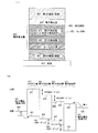
(実施の形態1)
本実施の形態1では、図2(A)に示すように基板200上に第1の電極201、電界発光層202、および第2の電極203が形成され、電界発光層202が第1の発光層211、第2の発光層212、および電子輸送層213からなる積層構造を有する場合について説明する。なお、第1の発光層211は、発光体を有し、第2の発光層212には、ホスト材料251と、発光体となる燐光材料252とが含まれており、燐光材料からは、燐光発光およびエキシマー発光が得られる。
(Embodiment 1)
In this
なお、第1の発光層211に用いる発光体(発光材料)としては、N,N’−ビス(3−メチルフェニル)−N,N’−ジフェニル−1,1’−ビフェニル−4,4’−ジアミン(略称:TPD)や、その誘導体である4,4'−ビス[N−(1−ナフチル)−N−フェニル−アミノ]−ビフェニル(略称:α−NPD)などのホール輸送性を持つ青色の蛍光材料や、ビス(2−メチル−8−キノリノラト)−(4−ヒドロキシ−ビフェニリル)−アルミニウム(略称:BAlq)、ビス[2−(2−ヒドロキシフェニル)−ベンゾオキサゾラト]亜鉛(略称:Zn(BOX)2)、などの電子輸送性を持つ青色の蛍光材料を用いればよい。また、青色の各種蛍光色素をゲスト材料として用いてもよく、ペリレン、9,10−ジフェニルアントラセン、クマリン系色素(クマリン30等)、などが挙げられる。さらに、燐光材料を用いてもよく、ビス(4,6−ジフルオロフェニル)ピリジナト−N,C2')(アセチルアセトナト)イリジウム(略称:Ir(Fppy)2(acac))等がある。これらは全て、400nm以上500nm以下に発光の最大ピークを示すため、本発明の第1の発光層211に用いる発光体として好適である。
Note that a light-emitting material (light-emitting material) used for the first light-emitting
また、第2の発光層212に用いる発光体(燐光材料)としては、白金を中心金属とする金属錯体が有効である。具体的には、下記構造式(1)〜(4)で示される物質を10wt%〜40wt%、好ましくは12.5wt%〜20wt%の濃度で存在させることにより、燐光発光とそのエキシマー発光の両方を得ることができる。ただし、本発明においてはこれらに限定されることはなく、燐光発光とエキシマー発光の両方を同時に発する燐光材料であれば何を用いてもよい。
As the light emitter (phosphorescent material) used for the second

なお、本発明の第1の発光層にゲスト材料を用いる場合や、第2の発光層において発光体と共に用いるホスト材料としては、以下に示す例に代表されるホール輸送材料や電子輸送材料を用いることができる。また、4,4’−N,N’−ジカルバゾリル−ビフェニル(略称:CBP)などのバイポーラ性の材料も用いることができる。 In addition, when using a guest material for the 1st light emitting layer of this invention, or a host material used with a light-emitting body in a 2nd light emitting layer, the hole transport material and electron transport material represented by the example shown below are used. be able to. Alternatively, a bipolar material such as 4,4′-N, N′-dicarbazolyl-biphenyl (abbreviation: CBP) can be used.
ホール輸送材料としては、芳香族アミン系(すなわち、ベンゼン環−窒素の結合を有するもの)の化合物が好適である。広く用いられている材料として、例えば、N,N’−ビス(3−メチルフェニル)−N,N’−ジフェニル−1,1’−ビフェニル−4,4’−ジアミン(略称:TPD)や、その誘導体である4,4'−ビス[N−(1−ナフチル)−N−フェニル−アミノ]−ビフェニル(略称:α−NPD)などがある。また、4,4',4''−トリス(N,N−ジフェニル−アミノ)−トリフェニルアミン(略称:TDATA)や、4,4',4''−トリス[N−(3−メチルフェニル)−N−フェニル−アミノ]−トリフェニルアミン(略称:MTDATA)などのスターバースト型芳香族アミン化合物が挙げられる。 As the hole transport material, an aromatic amine-based compound (that is, a compound having a benzene ring-nitrogen bond) is suitable. As a widely used material, for example, N, N′-bis (3-methylphenyl) -N, N′-diphenyl-1,1′-biphenyl-4,4′-diamine (abbreviation: TPD), 4,4'-bis [N- (1-naphthyl) -N-phenyl-amino] -biphenyl (abbreviation: α-NPD) which is a derivative thereof. In addition, 4,4 ′, 4 ″ -tris (N, N-diphenyl-amino) -triphenylamine (abbreviation: TDATA) and 4,4 ′, 4 ″ -tris [N- (3-methylphenyl) ) -N-phenyl-amino] -triphenylamine (abbreviation: MTDATA) and the like.
また、電子輸送材料としては、トリス(8−キノリノラト)アルミニウム(略称:Alq3)、トリス(4−メチル−8−キノリノラト)アルミニウム(略称:Almq3)、ビス(10−ヒドロキシベンゾ[h]−キノリナト)ベリリウム(略称:BeBq2)、BAlq、Zn(BOX)2、ビス[2−(2−ヒドロキシフェニル)−ベンゾチアゾラト]亜鉛(略称:Zn(BTZ)2)などの金属錯体が挙げられる。さらに、金属錯体以外にも、2−(4−ビフェニリル)−5−(4−tert−ブチルフェニル)−1,3,4−オキサジアゾール(略称:PBD)、1,3−ビス[5−(p−tert−ブチルフェニル)−1,3,4−オキサジアゾール−2−イル]ベンゼン(略称:OXD−7)などのオキサジアゾール誘導体、3−(4−tert−ブチルフェニル)−4−フェニル−5−(4−ビフェニリル)−1,2,4−トリアゾール(略称:TAZ)、3−(4−tert−ブチルフェニル)−4−(4−エチルフェニル)−5−(4−ビフェニリル)−1,2,4−トリアゾール(略称:p−EtTAZ)などのトリアゾール誘導体、2,2’,2”−(1,3,5−ベンゼントリイル)トリス[1−フェニル−1H−ベンズイミダゾール](略称:TPBI)のようなイミダゾール誘導体、バソフェナントロリン(略称:BPhen)、バソキュプロイン(略称:BCP)などのフェナントロリン誘導体等が挙げられる。 As an electron transporting material, tris (8-quinolinolato) aluminum (abbreviation: Alq 3 ), tris (4-methyl-8-quinolinolato) aluminum (abbreviation: Almq 3 ), bis (10-hydroxybenzo [h]- Metal complexes such as quinolinato) beryllium (abbreviation: BeBq 2 ), BAlq, Zn (BOX) 2 , and bis [2- (2-hydroxyphenyl) -benzothiazolate] zinc (abbreviation: Zn (BTZ) 2 ). In addition to metal complexes, 2- (4-biphenylyl) -5- (4-tert-butylphenyl) -1,3,4-oxadiazole (abbreviation: PBD), 1,3-bis [5- Oxadiazole derivatives such as (p-tert-butylphenyl) -1,3,4-oxadiazol-2-yl] benzene (abbreviation: OXD-7), 3- (4-tert-butylphenyl) -4 -Phenyl-5- (4-biphenylyl) -1,2,4-triazole (abbreviation: TAZ), 3- (4-tert-butylphenyl) -4- (4-ethylphenyl) -5- (4-biphenylyl) ) -1,2,4-triazole (abbreviation: p-EtTAZ) derivative, 2,2 ′, 2 ″-(1,3,5-benzenetriyl) tris [1-phenyl-1H-benzimidazole ] Examples thereof include imidazole derivatives such as (abbreviation: TPBI), phenanthroline derivatives such as bathophenanthroline (abbreviation: BPhen), bathocuproin (abbreviation: BCP), and the like.
なお、電子輸送層213には、上述した電子輸送材料を用いることができる。
Note that the electron transporting material described above can be used for the
次に、この構造を有する素子構造を形成する場合におけるバンドダイアグラムを図2(B)に示す。図中では、第1の電極201のHOMO準位(イオン化ポテンシャル)220、第1の発光層211のHOMO準位(イオン化ポテンシャル)221およびLUMO準位222、第2の発光層212のホスト材料の薄膜状態におけるHOMO準位(イオン化ポテンシャル)223およびLUMO準位224、第2の発光層212のゲスト材料(燐光材料)のHOMO準位(イオン化ポテンシャル)225およびLUMO準位226、電子輸送層213のHOMO準位(イオン化ポテンシャル)227およびLUMO準位228、第2の電極203のLUMO準位229を、それぞれ示してある。
Next, FIG. 2B shows a band diagram in the case of forming an element structure having this structure. In the figure, the HOMO level (ionization potential) 220 of the
この場合、第1の発光層211のイオン化ポテンシャル221と第2の発光層212全体(すなわち、第2の発光層のホスト材料251と燐光材料252とを含む状態)のイオン化ポテンシャル(ここでは、ホスト材料251のイオン化ポテンシャルを第2の発光層212全体のイオン化ポテンシャルとみなす)223とのエネルギーギャップ230が十分に大きい(具体的には、0.4eV以上)ことが好ましい。もし、エネルギーギャップ230が小さいと、第1の発光層211はホール輸送性であるため、第1の発光層211から第2の発光層212にホールが侵入し、最終的にキャリアのほとんどは第2の発光層212で再結合することになる。そうすると、第2の発光層212が緑色〜赤色領域の発光を呈するため、より短波長の青色発光を呈する第1の発光層211にエネルギー移動することができず、第2の発光層212のみが発光してしまう。
In this case, the
従って、エネルギーギャップ230を十分に大きくすることにより、キャリアの大多数が、第1の発光層211と第2の発光層212との界面近傍において再結合する。そして、少数のキャリアが第2の発光層212で再結合するか、部分的には燐光材料のHOMO準位214にトラップ、第1の発光層211および第2の発光層212の両方での発光を得ることができる。
Therefore, by making the
なお、第1の発光層211において、ホスト材料に青色発光を呈するゲスト材料を含む構成とする場合も同様である。すなわち、第1の発光層211全体(すなわち、第1の発光層のホスト材料と青色発光を呈するゲスト材料とを含む状態)のイオン化ポテンシャル221と第2の発光層212全体(第2の発光層のホスト材料251と燐光材料252とを含む状態)のイオン化ポテンシャル223とのエネルギーギャップ230が大きい(具体的には、0.4eV以上)ことが好ましい。
Note that the same applies to the first light-emitting
また、第2の発光層212全体(すなわち、第2の発光層のホスト材料221と燐光材料222とを含む状態)のイオン化ポテンシャル223と電子輸送層213のイオン化ポテンシャル227とのエネルギーギャップ231が大きい(具体的には、0.4eV以上)ことが好ましい。ここで、エネルギーギャップ231を大きくすることにより、キャリアであるホールを第2の発光層212に閉じ込めることができるため、第2の発光層212において効率的に再結合させることができる。
In addition, the
さらに、第1の発光層211のLUMO準位222と第2の発光層212全体(すなわち、第2の発光層のホスト材料251と燐光材料252とを含む状態)のLUMO準位(ここでは、ホスト材料のLUMO準位を第2の発光層全体のLUMO準位とみなす)224とのエネルギーギャップ232が大きい(具体的には、0.4eV以上)ことが好ましい。ここで、エネルギーギャップ232を大きくすることにより、キャリアである電子を第2の発光層212に閉じ込めることができるため、第2の発光層212において効率的に再結合させることができる。
Furthermore, the LUMO level (here, the state including the host material 251 and the phosphorescent material 252 of the second light emitting layer) of the
すなわち、本実施の形態1においては、エネルギーギャップ230、231、232を有するバンド構造とすることにより、より効率的に第1の発光層211および第2の発光層212からの発光を得ることができる。
That is, in the first embodiment, light emission from the first light-emitting
(実施の形態2)
本実施の形態2では、図3(A)に示すように基板300上に第1の電極301、電界発光層302、および第2の電極303が形成され、電界発光層302が第1の発光層311、および第2の発光層312からなる積層構造を有する場合について説明する。なお、第2の発光層312には、ホスト材料351と、燐光材料352とが含まれており、燐光材料からは、燐光発光およびエキシマー発光が得られる。
(Embodiment 2)
In
本実施の形態2における構造は、実施の形態1で示した構造のうち、電界発光層に電子輸送層を含まない構造であり、電子輸送層を形成する工程を減らすことができるというメリットを有している。なお、発光効率を維持するために第2の発光層312のホスト材料321に電子輸送性に優れた材料を用いることが好ましい。
The structure in
なお、本実施の形態2の場合において、第1の発光層311、および第2の発光層312に用いる材料は、実施の形態1に示した材料と同じ材料を用いることができる。
Note that in the case of
次に、この構造を有する素子構造を形成する場合におけるバンドダイアグラムを図3(B)に示す。図中では、第1の電極301のHOMO準位(イオン化ポテンシャル)320、第1の発光層311のHOMO準位(イオン化ポテンシャル)321およびLUMO準位322、第2の発光層312のホスト材料の薄膜状態におけるHOMO準位(イオン化ポテンシャル)323およびLUMO準位324、第2の発光層312のゲスト材料(燐光材料)のHOMO準位(イオン化ポテンシャル)325およびLUMO準位326、第2の電極303のLUMO準位327を、それぞれ示してある。
Next, a band diagram in the case of forming an element structure having this structure is shown in FIG. In the figure, the HOMO level (ionization potential) 320 of the
本実施の形態2の場合においても、第1の発光層311および第2の発光層312からの発光をより効率的に得るためには、第1の発光層311のイオン化ポテンシャル321と第2の発光層312全体(すなわち、第2の発光層のホスト材料351と燐光材料352とを含む状態)のイオン化ポテンシャル(ここでは、ホスト材料351のイオン化ポテンシャルを第2の発光層312全体のイオン化ポテンシャルとみなす)323とのエネルギーギャップ341が実施の形態1の場合と同様に十分に大きい(具体的には、0.4eV以上)ことが好ましく、さらに第1の発光層311のLUMO準位322と第2の発光層312全体(すなわち、第2の発光層のホスト材料351と燐光材料352とを含む状態)のLUMO準位(ここでは、ホスト材料351のLUMO準位を第2の発光層312全体のLUMO準位とみなす)324とのエネルギーギャップ342が実施の形態1の場合と同様に十分に大きい(具体的には、0.3eV以上)ことが好ましい。
Also in the case of the second embodiment, in order to obtain light emission from the first
なお、第1の発光層311において、ホスト材料に青色発光を呈するゲスト材料を含む構成とする場合も同様である。すなわち、第1の発光層311全体(すなわち、第1の発光層のホスト材料と青色発光を呈するゲスト材料とを含む状態)のイオン化ポテンシャル(ここでは、第1の発光層のホスト材料のイオン化ポテンシャルを第1の発光層311全体のイオン化ポテンシャルとみなす)321と第2の発光層312全体(第2の発光層のホスト材料351と燐光材料352とを含む状態)のイオン化ポテンシャル323とのエネルギーギャップ341が大きい(具体的には、0.4eV以上)ことが好ましい。
Note that the same applies to the case where the first light-emitting
(実施の形態3)
本実施の形態3では、図4(A)に示すように基板400上に第1の電極401、電界発光層402、および第2の電極403が形成され、電界発光層402がホール注入層411、第1の発光層412、第2の発光層413、および電子輸送層414からなる積層構造を有する場合について説明する。なお、第2の発光層413には、ホスト材料451と、燐光材料452とが含まれており、燐光材料からは、燐光発光およびエキシマー発光が得られる。
(Embodiment 3)
In
ホール注入層411に用いる材料としては、先に示したTPD、α−NPD、TDATA、MTDATA等の上述したホール輸送材料の他、以下に示すホール輸送材料を用いることができる。
As a material used for the
ホール注入材料としては、有機化合物であればポルフィリン系の化合物が有効であり、フタロシアニン(略称:H2−Pc)、銅フタロシアニン(略称:Cu−Pc)等を用いることができる。また、導電性高分子化合物に化学ドーピングを施した材料もあり、ポリスチレンスルホン酸(略称:PSS)をドープしたポリエチレンジオキシチオフェン(略称:PEDOT)や、ポリアニリン(略称:PAni)、ポリビニルカルバゾール(略称:PVK)などを用いることもできる。また、五酸化バナジウムのような無機半導体の薄膜や、酸化アルミニウムなどの無機絶縁体の超薄膜も有効である。 The hole injection material, it is effective to a porphyrin-based compound as long as it is an organic compound, phthalocyanine (abbreviation: H 2 -Pc), copper phthalocyanine (abbreviation: Cu-Pc), or the like can be used. There are also materials obtained by chemically doping conductive polymer compounds, such as polyethylenedioxythiophene (abbreviation: PEDOT) doped with polystyrene sulfonic acid (abbreviation: PSS), polyaniline (abbreviation: PAni), and polyvinylcarbazole (abbreviation). : PVK) can also be used. In addition, an inorganic semiconductor thin film such as vanadium pentoxide or an ultra-thin film of an inorganic insulator such as aluminum oxide is also effective.
また、第1の発光層412、第2の発光層413、および電子輸送層414に用いる発光体、もしくは材料としては、実施の形態1に示したものと同じ材料をそれぞれ用いることができる。
As the light-emitting body or material used for the first light-emitting
次に、この構造を有する素子構造を形成する場合におけるバンドダイアグラムを図4(B)に示す。図中では、第1の電極401のHOMO準位(イオン化ポテンシャル)420、ホール注入層411のHOMO準位(イオン化ポテンシャル)421およびLUMO準位422、第1の発光層412のHOMO準位(イオン化ポテンシャル)423およびLUMO準位424、第2の発光層413のホスト材料におけるHOMO準位(イオン化ポテンシャル)425およびLUMO準位426、第2の発光層413のゲスト材料(燐光材料)のHOMO準位(イオン化ポテンシャル)427およびLUMO準位428、電子輸送層414のHOMO準位(イオン化ポテンシャル)429およびLUMO準位430、第2の電極403のLUMO準位431を、それぞれ示してある。
Next, FIG. 4B shows a band diagram in the case of forming an element structure having this structure. In the figure, the HOMO level (ionization potential) 420 of the
なお、本実施の形態3において示す構造は、実施の形態1に示した構造に、ホール注入層411が加わった構造を有している。
Note that the structure shown in
本実施の形態3の場合には、第1の発光層412および第2の発光層413からの発光をより効率的に得るためには、第1の発光層412のイオン化ポテンシャル423と第2の発光層413全体(すなわち、第2の発光層のホスト材料451と燐光材料452とを含む状態)のイオン化ポテンシャル(ここでは、ホスト材料451のイオン化ポテンシャルを第2の発光層413全体のイオン化ポテンシャルとみなす)425とのエネルギーギャップ441が十分に大きい(具体的には、0.4eV以上)ことが好ましく、第2の発光層413全体(すなわち、第2の発光層のホスト材料451と燐光材料452とを含む状態)のイオン化ポテンシャル425と電子輸送層414のイオン化ポテンシャル429とのエネルギーギャップ442が、十分に大きい(具体的には、0.4eV以上)ことが好ましく、さらに、第1の発光層412のLUMO準位424と第2の発光層413全体(すなわち、第2の発光層のホスト材料451と燐光材料452とを含む状態)のLUMO準位(ここでは、ホスト材料451のLUMO準位を第2の発光層413全体のLUMO準位とみなす)426とのエネルギーギャップ443が実施の形態1の場合と同様に十分に大きい(具体的には、0.3eV以上)ことが好ましい。さらに、ホール注入層411のLUMO準位422と第1の発光層412のLUMO準位423とのエネルギーギャップ444が十分に大きい(具体的には、0.3eV以上)ことが好ましい。
In the case of
なお、このようにホール注入層411のLUMO準位422と第1の発光層412のLUMO準位423とのエネルギーギャップ444を確保することにより、第1の発光層412に電子を閉じ込めることができるので、第1の発光層412におけるキャリアの再結合を効率よく行うことができる。
Note that by securing the energy gap 444 between the
また、第1の発光層412において、ホスト材料に青色発光を呈するゲスト材料を含む構成とする場合も同様である。すなわち、第1の発光層412全体(すなわち、第1の発光層のホスト材料と青色発光を呈するゲスト材料とを含む状態)のイオン化ポテンシャル(ここでは、第1の発光層のホスト材料のイオン化ポテンシャルを第1の発光層412全体のイオン化ポテンシャルとみなす)423と第2の発光層413全体(第2の発光層のホスト材料451と燐光材料452とを含む状態)のイオン化ポテンシャル425とのエネルギーギャップ441が大きい(具体的には、0.4eV以上)ことが好ましい。
The same applies to the case where the first light-emitting
以上のようにして、実施の形態1〜3で示した代表的な構造を有する本発明を適用すれば、このように単純な素子構造で赤色、緑色、青色の各波長領域にピークを持つ白色発光素子が達成できる。
As described above, when the present invention having the typical structure shown in
なお、上述した構造は、本発明における好ましい構造の一例に過ぎず、本発明の発光素子の電界発光層は、少なくとも上述した第1の発光層と第2の発光層とを含めばよい。すなわち、ここでは、挙げなかったが、従来の発光素子で知られているような、発光以外の機能を示す層(例えば、電子注入層等)を適宜組み合わせてもよい。 Note that the above-described structure is merely an example of a preferable structure in the present invention, and the electroluminescent layer of the light-emitting element of the present invention may include at least the first light-emitting layer and the second light-emitting layer described above. That is, although not mentioned here, layers showing functions other than light emission (such as an electron injection layer) as known in conventional light emitting elements may be combined as appropriate.
電子注入層に用いることができる電子注入材料としては、上述した電子輸送材料を用いることができる。その他に、LiF、CsFなどのアルカリ金属ハロゲン化物や、CaF2のようなアルカリ土類ハロゲン化物、Li2Oなどのアルカリ金属酸化物のような絶縁体の超薄膜がよく用いられる。また、リチウムアセチルアセトネート(略称:Li(acac)や8−キノリノラト−リチウム(略称:Liq)などのアルカリ金属錯体も有効である。 As the electron injecting material that can be used for the electron injecting layer, the above-described electron transporting material can be used. In addition, an ultra-thin film of an insulator such as an alkali metal halide such as LiF or CsF, an alkaline earth halide such as CaF 2 , or an alkali metal oxide such as Li 2 O is often used. In addition, alkali metal complexes such as lithium acetylacetonate (abbreviation: Li (acac) and 8-quinolinolato-lithium (abbreviation: Liq) are also effective.
また、本発明の発光素子は、発光を取り出すために少なくともどちらか一方の電極が透明な材料で形成されていれば良いため、通常、基板上に形成される第1の電極が透明である構造(下面出射構造ともいう)や、第1の電極上に電界発光層を形成した後積層される第2の電極が透明である構造(上面出射構造ともいう)、さらに、両方の電極が透明である構造(両面出射構造ともいう)とすることもできる。 In the light-emitting element of the present invention, since at least one of the electrodes only needs to be formed of a transparent material in order to extract light emission, the first electrode formed on the substrate is usually transparent. (Also referred to as a bottom emission structure), a structure in which the second electrode laminated after forming the electroluminescent layer on the first electrode is transparent (also referred to as a top emission structure), and both electrodes are transparent. A certain structure (also referred to as a dual emission structure) may be employed.
なお、本実施の形態1〜3に示した第1の電極(201、301、401)、または第2の電極(203、303、403)のいずれか一方に用いる陽極材料としては、仕事関数の大きい導電性材料を用いることが好ましい。陽極側を光の取り出し方向とするのであれば、インジウム−スズ酸化物(ITO)、インジウム−亜鉛酸化物(IZO)等の透明導電性材料を用いればよい。また、陽極側を遮光性とするのであれば、TiN、ZrN、Ti、W、Ni、Pt、Cr等の単層膜の他、窒化チタンとアルミニウムを主成分とする膜との積層、窒化チタン膜とアルミニウムを主成分とする膜と窒化チタン膜との三層構造等を用いることができる。あるいは、Ti、Al等の反射性電極の上に上述した透明導電性材料を積層する方法でもよい。 Note that an anode material used for either the first electrode (201, 301, 401) or the second electrode (203, 303, 403) described in the first to third embodiments is a work function. It is preferable to use a large conductive material. If the anode side is the light extraction direction, a transparent conductive material such as indium-tin oxide (ITO) or indium-zinc oxide (IZO) may be used. If the anode side is to be light-shielding, a single layer film such as TiN, ZrN, Ti, W, Ni, Pt, Cr, etc., a laminate of titanium nitride and a film mainly composed of aluminum, titanium nitride A three-layer structure of a film, a film containing aluminum as its main component, and a titanium nitride film can be used. Or the method of laminating | stacking the transparent conductive material mentioned above on reflective electrodes, such as Ti and Al, may be used.
また、陰極材料としては、仕事関数の小さい導電性材料を用いることが好ましく、具体的には、LiやCs等のアルカリ金属、およびMg、Ca、Sr等のアルカリ土類金属、およびこれらを含む合金(Mg:Ag、Al:Li、Li:Agなど)の他、YbやEr等の希土類金属を用いて形成することもできる。また、LiF、CsF、CaF2、Li2O等の電子注入層を用いる場合は、アルミニウム等の通常の導電性薄膜を用いることができる。また、陰極側を光の取り出し方向とする場合は、LiやCs等のアルカリ金属、およびMg、Ca、Sr等のアルカリ土類金属を含む超薄膜と、透明導電膜(ITO、IZO、ZnO等)との積層構造を用いればよい。あるいは、アルカリ金属またはアルカリ土類金属と電子輸送材料を共蒸着した電子注入層を形成し、その上に透明導電膜(ITO、IZO、ZnO等)を積層してもよい。 Moreover, it is preferable to use a conductive material having a small work function as the cathode material. Specifically, the cathode material includes alkali metals such as Li and Cs, alkaline earth metals such as Mg, Ca, and Sr, and these. In addition to alloys (Mg: Ag, Al: Li, Li: Ag, etc.), they can also be formed using rare earth metals such as Yb and Er. Further, LiF, CsF, in the case of using an electron injecting layer such as CaF 2, Li 2 O, may be used usual conductive thin film such as aluminum. When the cathode side is the light extraction direction, an ultrathin film containing an alkali metal such as Li or Cs and an alkaline earth metal such as Mg, Ca, or Sr, and a transparent conductive film (ITO, IZO, ZnO, etc.) ) And a stacked structure may be used. Alternatively, an electron injection layer in which an alkali metal or an alkaline earth metal and an electron transport material are co-evaporated may be formed, and a transparent conductive film (ITO, IZO, ZnO, or the like) may be stacked thereon.
なお、以上で述べた本発明の発光素子を作製するに当たっては、発光素子中の各層の積層法を限定されるものではない。積層が可能ならば、真空蒸着法やスピンコート法、インクジェット法、ディップコート法など、どの様な手法を選んでも良いものとする。 Note that in manufacturing the light-emitting element of the present invention described above, the stacking method of each layer in the light-emitting element is not limited. As long as lamination is possible, any method such as a vacuum deposition method, a spin coating method, an ink jet method, or a dip coating method may be selected.
以下に、本発明の実施例について説明する。 Examples of the present invention will be described below.
本実施例では、本発明の発光素子の素子構造および作製方法について、図5を用いて説明する。 In this example, an element structure and a manufacturing method of a light-emitting element of the present invention will be described with reference to FIGS.
まず、絶縁表面を有するガラス基板500上に発光素子の陽極501が形成される。材料として透明導電膜であるITOを用い、スパッタリング法により110nmの膜厚で形成する。陽極501の形状は、2mm×2mmの大きさとする。
First, an
次に、陽極501上に電界発光層502が形成される。なお、本実施例では、電界発光層502がホール注入層511、正孔輸送性の第1の発光層512、第2の発光層513、電子輸送層514、電子注入層515からなる積層構造とした。第1の発光層512には、その発光が青色である材料、具体的には、発光スペクトルの最大ピークが400〜500nmである材料を用いる。また、第2の発光層513には、ホスト材料および燐光発光を呈するゲスト材料を用いる。
Next, the
はじめに、陽極501が形成された基板を真空蒸着装置の基板ホルダーに陽極501が形成された面を下方にして固定し、真空蒸着装置の内部に備えられた蒸発源にCu−Pcを入れ、抵抗加熱法を用いた真空蒸着法により20nmの膜厚でホール注入層511を形成する。
First, the substrate on which the
次に、正孔輸送性および発光性に優れた材料により第1の発光層512を形成する。ここでは、α−NPDを同様の方法により、30nmの膜厚で形成する。
Next, the first light-emitting
さらに、第2の発光層513を形成する。なお、本実施例では、ホスト材料521としてCBPを用い、ゲスト材料(燐光材料)522として上記構造式(1)で表されるPt(ppy)acacを用い、その濃度が15wt%となるように調整し、共蒸着法により20nmの膜厚で形成する。 Further, a second light emitting layer 513 is formed. In this embodiment, CBP is used as the host material 521, Pt (ppy) acac represented by the structural formula (1) is used as the guest material (phosphorescent material) 522, and the concentration thereof is 15 wt%. It is adjusted and formed with a film thickness of 20 nm by a co-evaporation method.
また、第2の発光層513の上には電子輸送層514が形成される。なお、電子輸送層514は、BCP(バソキュプロイン)を用いて、蒸着法により20nmの膜厚で形成する。その上に、電子注入層515としてCaF2を2nm形成し、積層構造を有する電界発光層502を形成する。
In addition, an electron transport layer 514 is formed over the second light-emitting layer 513. Note that the electron-transport layer 514 is formed with a thickness of 20 nm by a vapor deposition method using BCP (bathocuproin). On top of this, 2 nm of CaF 2 is formed as the
最後に、陰極503を形成する。なお、本実施例では、アルミニウム(Al)を抵抗加熱による真空蒸着法により100nm形成し陰極503を形成する。
Finally, the
以上により、本発明の発光素子が形成される。なお、本実施例に示す構造では、第1の発光層512および第2の発光層513においてそれぞれ発光が得られるため、全体として白色発光を呈する素子を形成することができる。
Thus, the light emitting element of the present invention is formed. Note that in the structure shown in this embodiment, light emission can be obtained in each of the first light-emitting
なお、本実施例では、基板上に陽極を形成する場合について説明したが、本発明はこれに限定されることはなく、基板上に陰極を形成することもできる。ただし、この場合(すなわち陽極と陰極とを入れ替えた場合)には、電界発光層の積層順が本実施例で示した場合と逆になる。 In this embodiment, the case where the anode is formed on the substrate has been described. However, the present invention is not limited to this, and the cathode can be formed on the substrate. However, in this case (that is, when the anode and the cathode are interchanged), the order of stacking the electroluminescent layers is reversed from the case shown in this embodiment.
さらに、本実施例では、陽極501は透明電極であり、陽極501側から電界発光層502で生じた光を出射させる構成としているが、本発明はこれに限定されることはなく、透過率を確保するために適した材料を選択することにより陰極503側から光を出射させる構成とすることもできる。
Further, in this embodiment, the
本実施例では、実施例1で示した素子構造を有する発光素子(ITO/Cu−Pc(20nm)/α−NPD(30nm)/CBP+Pt(ppy)acac:15wt%(20nm)/BCP(30nm)/CaF(2nm)/Al(100nm))の素子特性について説明する。なお、上記構造を有する発光素子の発光スペクトルを図8のスペクトル1、および図9に示す。また、電気的特性について図10〜図13のプロット1に示す。
In this example, a light-emitting element having the element structure shown in Example 1 (ITO / Cu—Pc (20 nm) / α-NPD (30 nm) / CBP + Pt (ppy) acac: 15 wt% (20 nm) / BCP (30 nm) The device characteristics of / CaF (2 nm) / Al (100 nm)) will be described. Note that an emission spectrum of the light-emitting element having the above structure is illustrated in FIG. 8 and FIG. Moreover, it shows in the
図8のスペクトル1は、上記構造を有する発光素子に1mAの電流を流した際(約960cd/m2時)の発光スペクトルである。スペクトル1に示す結果から、第一発光層を形成するα−NPDの青色(〜450nm)、第二発光層に含まれるPt(ppy)acacの燐光発光による緑色(〜490nmおよび〜530nm)、第二発光層に含まれるPt(ppy)acacのエキシマー発光による橙色(〜570nm)の3成分を持つ白色発光が得られることがわかる。CIE色度座標は、(x、y)=(0.346、0.397)であり、見た目にもほぼ白色であった。
ここで、第一発光層に用いたα−NPDおよび第二発光層のホスト材料に用いたCBPのイオン化ポテンシャルを測定したところ、α−NPDは約5.3eV、CBPは約5.9eVであり、その差は約0.6eVであった。すなわち、0.4eV以上という本発明の好ましい条件を満たしており、このことが良好な白色発光につながっていると考えられる。なお、イオン化ポテンシャルの測定は、光電子分光装置AC−2(理研計器社製)を用いて行った。 Here, when the ionization potential of α-NPD used for the first light emitting layer and CBP used for the host material of the second light emitting layer was measured, α-NPD was about 5.3 eV, and CBP was about 5.9 eV. The difference was about 0.6 eV. That is, the preferable condition of the present invention of 0.4 eV or more is satisfied, and this is considered to lead to good white light emission. The ionization potential was measured using a photoelectron spectrometer AC-2 (manufactured by Riken Keiki Co., Ltd.).
また、図9は、上記構造を有する発光素子に流す電流量を変化させた場合の各スペクトルを測定した結果である。ここでは、スペクトルa(0.1mA)、スペクトルb(1mA)、スペクトルc(5mA)と電流値を変化させた場合の測定結果を示す。この結果から明らかなように、電流値を増加させても(輝度を上げても)、スペクトル形状はほとんど変化せず、本発明の発光素子が電流値の変化に影響を受けない安定した白色発光を示すことがわかった。 FIG. 9 shows the results of measuring each spectrum when the amount of current flowing through the light-emitting element having the above structure is changed. Here, the measurement results when the spectrum a (0.1 mA), the spectrum b (1 mA), the spectrum c (5 mA), and the current value are changed are shown. As is clear from this result, even when the current value is increased (increasing the brightness), the spectrum shape hardly changes, and the light-emitting element of the present invention is not affected by the change in the current value. It was found that
上記構造を有する発光素子の電気的特性として、図10における輝度−電流特性においては、プロット1に示すように、電流密度が10mA/cm2の場合において460cd/m2程度の輝度が得られた。
As the electrical characteristics of the light-emitting element having the above structure, in the luminance-current characteristics in FIG. 10, as shown in
また、図11に示す輝度−電圧特性においては、プロット1に示すように、9Vの電圧を印加したところ120cd/m2程度の輝度が得られた。
In the luminance-voltage characteristics shown in FIG. 11, when a voltage of 9 V was applied as shown in
また、図12に示す電流効率−輝度特性においては、プロット1に示すように、100cd/m2の輝度が得られた場合における電流効率は4.6cd/A程度であった。
In the current efficiency-luminance characteristics shown in FIG. 12, as shown in
さらに、図13に示す電流−電圧特性においては、プロット1に示すように、9Vの電圧を印加したところ0.12mA程度の電流が流れた。
Furthermore, in the current-voltage characteristics shown in FIG. 13, when a voltage of 9 V was applied as shown in
また、ICP−MSにより、上述した発光素子中におけるPtの量を定量したところ、Ptの量は21ngであった。単位面積あたりの原子濃度に換算すると、5.4×10¹⁴atoms/cm2であった。 Further, when the amount of Pt in the light-emitting element described above was quantified by ICP-MS, the amount of Pt was 21 ng. In terms of atomic concentration per unit area, it was 5.4 × 10 14 atoms / cm 2 .
さらに、二次イオン質量分析(Secondary Ion Mass Spectrometry:SIMS)によってPt濃度の深さ方向分析を行い、上述のPtの量を元に換算して、Ptの単位体積あたりの濃度を算出した。その結果、Ptの単位体積あたりの濃度の最大値は、2.0×10²⁰atoms/cm3程度であった。モル濃度に換算すると、3.3×10-4mol/cm3となる。したがって、エキシマーを形成する燐光材料の濃度が10-4〜10-3mol/cm3であれば、エキシマー発光が可能になると考えられる。 Further, Pt concentration in the depth direction was analyzed by secondary ion mass spectrometry (SIMS), and the Pt concentration per unit volume was calculated based on the amount of Pt described above. As a result, the maximum concentration of Pt per unit volume was about 2.0 × 10 20 atoms / cm 3 . When converted to a molar concentration, it becomes 3.3 × 10 −4 mol / cm 3 . Therefore, if the concentration of the phosphorescent material forming the excimer is 10 −4 to 10 −3 mol / cm 3 , excimer emission is considered possible.
また、上述の通り、Ptの単位体積あたりの濃度の最大値は2.0×10²⁰atoms/cm3であることから、Pt錯体1個が占める平均体積は、5.0×10-27m3/atomとなる。つまり、Pt錯体が均一に分散していると考えた場合、Pt錯体は1.7nm立方に1個の割合で分散していることになる。したがってこの場合、燐光材料の金属原子(本実施例ではPt原子)間の距離は、17Å程度である。以上の結果から、本発明においては、燐光材料の中心金属間の距離は20Å以下であることが好ましいと言える。 Further, as described above, since the maximum value of the Pt concentration per unit volume is 2.0 × 10 20 atoms / cm 3 , the average volume occupied by one Pt complex is 5.0 × 10 −27 m. 3 / atom. That is, when it is considered that the Pt complex is uniformly dispersed, the Pt complex is dispersed at a rate of one per 1.7 nm cube. Therefore, in this case, the distance between the metal atoms (Pt atoms in this embodiment) of the phosphorescent material is about 17 mm. From the above results, in the present invention, it can be said that the distance between the central metals of the phosphorescent material is preferably 20 mm or less.
[比較例1]
これに対して、実施例1で示した場合と発光層に含まれるPt(ppy)acacの濃度を変えて作製した発光素子の発光スペクトルを、図8のスペクトル2およびスペクトル3に示す。なお、Pt(ppy)acacの濃度が、7.9wt%の場合における測定結果がスペクトル2、2.5wt%の場合における測定結果がスペクトル3である。また、いずれの場合も、素子に1mAの電流を流した際のスペクトルである。
[Comparative Example 1]
In contrast, the emission spectra of the light-emitting elements manufactured by changing the concentration of Pt (ppy) acac contained in the light-emitting layer as shown in Example 1 are shown in
スペクトル3で示されるように、2.5wt%の濃度では、第一発光層を形成するα−NPDの青色(〜450nm)と、第二発光層に含まれるPt(ppy)acacの緑色(〜490nmおよび530nm)のみしか観測されず、その結果白色発光とはならなかった。また、スペクトル2で示されるように、7.9wt%の濃度においては、わずかにPt(ppy)acacのエキシマー発光が560nm付近にショルダーとしてスペクトルに加わっているものの、そのピークは十分ではなく、十分な白色は得られなかった。
As shown in
また、これらの素子の電気的特性を測定した。Pt(ppy)acacの濃度が7.9wt%の素子の測定結果を図10〜13のプロット2に示し、2.5wt%の素子の測定結果を図10〜13のプロット3に示す。
In addition, the electrical characteristics of these elements were measured. The measurement results of the element having a Pt (ppy) acac concentration of 7.9 wt% are shown in
図10における輝度−電流特性においては、電流密度が10mA/cm2の場合、7.9wt%の素子は180cd/m2程度の輝度が得られ、2.5wt%の素子は115cd/m2程度の輝度が得られた。 Brightness in Figure 10 - In current characteristics, current densities of 10 mA / cm 2, elements of 7.9 wt% is obtained luminance of about 180 cd / m 2, elements of 2.5 wt% is 115cd / m 2 about Was obtained.
また、図11に示す輝度−電圧特性においては、9Vの電圧を印加したところ、7.9wt%の素子は93cd/m2程度の輝度が得られ、2.5wt%の素子は73cd/m2程度の輝度が得られた。 The luminance shown in FIG. 11 - In the voltage characteristics, was applied with a voltage of 9V, elements of 7.9 wt% is obtained luminance of about 93cd / m 2, elements of 2.5 wt% is 73cd / m 2 A degree of brightness was obtained.
また、図12に示す電流効率−輝度特性においては、100cd/m2の輝度が得られた場合、7.9wt%の素子の電流効率は1.8cd/A程度であり、2.5wt%の素子の電流効率は1.1cd/A程度であった。 In the current efficiency-luminance characteristics shown in FIG. 12, when a luminance of 100 cd / m 2 is obtained, the current efficiency of a 7.9 wt% element is about 1.8 cd / A, and 2.5 wt%. The current efficiency of the device was about 1.1 cd / A.
さらに、図13に示す電流−電圧特性においては、9Vの電圧を印加したところ、7.9wt%の素子は0.21mA程度の電流が流れ、2.5wt%の素子は0.27mA程度の電流が流れた。 Furthermore, in the current-voltage characteristics shown in FIG. 13, when a voltage of 9 V is applied, a current of about 0.21 mA flows through a 7.9 wt% element, and a current of about 0.27 mA flows through a 2.5 wt% element. Flowed.
以上の結果から(特に、図13に示す電流−電圧特性の結果から)、本発明の発光素子はゲスト材料であるPt(ppy)acacの濃度が高濃度(15wt%)であるにもかかわらず、低濃度(7.9wt%、2.5wt%)で形成された発光素子と同程度の電気特性を有していることがわかる。 From the above results (particularly, from the results of the current-voltage characteristics shown in FIG. 13), the light-emitting element of the present invention has a high concentration (15 wt%) of Pt (ppy) acac as a guest material. It can be seen that the light-emitting element formed at a low concentration (7.9 wt%, 2.5 wt%) has the same electrical characteristics.
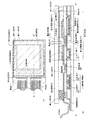
本実施例では、絶縁表面を有する基板上に、本発明の白色発光を呈する発光素子を備えた発光装置(上面出射構造)を作製する例を図6に示す。なお、上面出射構造とは、絶縁表面を有する基板とは逆側から光を取り出す構造である。 In this embodiment, an example of manufacturing a light-emitting device (a top emission structure) including a light-emitting element that emits white light according to the present invention over a substrate having an insulating surface is shown in FIG. Note that the top emission structure is a structure in which light is extracted from a side opposite to a substrate having an insulating surface.
図6(A)は、発光装置を示す上面図、図6(B)は図6(A)をA−A’で切断した断面図である。点線で示された601はソース信号線駆動回路、602は画素部、603はゲート側駆動回路である。また、604は透明な封止基板、605は第1シール材であり、第1シール材605で囲まれた内側は、透明な第2シール材607で充填されている。なお、第1シール材605には基板間隔を保持するためのギャップ材が含有されている。 6A is a top view illustrating the light-emitting device, and FIG. 6B is a cross-sectional view taken along line A-A ′ in FIG. 6A. Reference numeral 601 indicated by a dotted line denotes a source signal line driver circuit, 602 denotes a pixel portion, and 603 denotes a gate side driver circuit. Reference numeral 604 denotes a transparent sealing substrate, reference numeral 605 denotes a first sealing material, and the inside surrounded by the first sealing material 605 is filled with a transparent second sealing material 607. Note that the first sealing material 605 contains a gap material for maintaining the distance between the substrates.
なお、608は、ソース側駆動回路601及びゲート側駆動回路603に入力される信号を伝送するための接続配線であり、外部入力端子となるFPC(フレキシブルプリントサーキット)609からビデオ信号やクロック信号を受け取る。なお、ここではFPCしか図示されていないが、このFPCにはプリント配線基盤(PWB)が取り付けられていても良い。 Reference numeral 608 denotes a connection wiring for transmitting a signal input to the source side driver circuit 601 and the gate side driver circuit 603, and a video signal and a clock signal are received from an FPC (flexible printed circuit) 609 serving as an external input terminal. receive. Although only the FPC is shown here, a printed wiring board (PWB) may be attached to the FPC.
次に、断面構造について図6(B)を用いて説明する。基板610上には駆動回路及び画素部が形成されているが、ここでは、駆動回路としてソース側駆動回路601と画素部602が示されている。 Next, a cross-sectional structure will be described with reference to FIG. A driver circuit and a pixel portion are formed over the substrate 610. Here, a source side driver circuit 601 and a pixel portion 602 are shown as driver circuits.
なお、ソース側駆動回路601はnチャネル型TFT623とpチャネル型TFT624とを組み合わせたCMOS回路が形成される。また、駆動回路を形成するTFTは、公知のCMOS回路、PMOS回路もしくはNMOS回路で形成しても良い。また、本実施例では、基板上に駆動回路を形成したドライバー一体型を示すが、必ずしもその必要はなく、基板上ではなく外部に形成することもできる。また、ポリシリコン膜を活性層とするTFTの構造は特に限定されず、トップゲート型TFTであってもよいし、ボトムゲート型TFTであってもよい。
Note that the source side driver circuit 601 is a CMOS circuit in which an n-
また、画素部602はスイッチング用TFT611と、電流制御用TFT612とそのドレインに電気的に接続された第1の電極(陽極)613を含む複数の画素により形成される。電流制御用TFT612としてはnチャネル型TFTであってもよいし、pチャネル型TFTであってもよいが、陽極と接続させる場合、pチャネル型TFTとすることが好ましい。また、保持容量(図示しない)を適宜設けることが好ましい。なお、ここでは無数に配置された画素のうち、一つの画素の断面構造のみを示し、その一つの画素に2つのTFTを用いた例を示したが、3つ、またはそれ以上のTFTを適宜、用いてもよい。
The pixel portion 602 is formed of a plurality of pixels including a switching
ここでは第1の電極(陽極)613がTFTのドレインと直接接している構成となっているため、第1の電極(陽極)613の下層はシリコンからなるドレインとオーミックコンタクトのとれる材料層とし、有機化合物を含む層と接する最上層を仕事関数の大きい材料層とすることが望ましい。例えば、窒化チタン膜とアルミニウムを主成分とする膜と窒化チタン膜との3層構造とすると、配線としての抵抗も低く、且つ、良好なオーミックコンタクトがとれ、且つ、陽極として機能させることができる。また、第1の電極(陽極)613は、窒化チタン膜、クロム膜、タングステン膜、Zn膜、Pt膜などの単層としてもよいし、3層以上の積層を用いてもよい。 Here, since the first electrode (anode) 613 is in direct contact with the drain of the TFT, the lower layer of the first electrode (anode) 613 is a material layer that can be in ohmic contact with the drain made of silicon, The uppermost layer in contact with the layer containing an organic compound is preferably a material layer having a high work function. For example, when a three-layer structure of a titanium nitride film, a film containing aluminum as a main component, and a titanium nitride film is used, the resistance as a wiring is low, a good ohmic contact can be obtained, and the film can function as an anode. . The first electrode (anode) 613 may be a single layer such as a titanium nitride film, a chromium film, a tungsten film, a Zn film, or a Pt film, or may be a stack of three or more layers.
また、第1の電極(陽極)613の両端には絶縁物(バンク、隔壁、障壁、土手などと呼ばれる)614が形成される。絶縁物614は有機樹脂膜もしくは珪素を含む絶縁膜で形成すれば良い。ここでは、絶縁物614として、ポジ型の感光性アクリル樹脂膜を用いて図6に示す形状の絶縁物を形成する。 In addition, insulators (referred to as banks, partition walls, barriers, banks, or the like) 614 are formed on both ends of the first electrode (anode) 613. The insulator 614 may be formed using an organic resin film or an insulating film containing silicon. Here, as the insulator 614, a positive-type photosensitive acrylic resin film is used to form the insulator having the shape shown in FIG.
成膜性を良好なものとするため、絶縁物614の上端部または下端部に曲率を有する曲面が形成されるようにする。例えば、絶縁物614の材料としてポジ型の感光性アクリルを用いた場合、絶縁物614の上端部のみに曲率半径(0.2μm〜3μm)を有する曲面を持たせることが好ましい。また、絶縁物614として、感光性の光によってエッチャントに不溶解性となるネガ型、或いは光によってエッチャントに溶解性となるポジ型のいずれも使用することができる。 In order to improve the film forming property, a curved surface having a curvature is formed at the upper end portion or the lower end portion of the insulator 614. For example, when positive photosensitive acrylic is used as a material for the insulator 614, it is preferable that only the upper end portion of the insulator 614 has a curved surface with a curvature radius (0.2 μm to 3 μm). As the insulator 614, either a negative type that becomes insoluble in an etchant by photosensitive light or a positive type that becomes soluble in an etchant by light can be used.
また、絶縁物614を窒化アルミニウム膜、窒化酸化アルミニウム膜、炭素を主成分とする薄膜、または窒化珪素膜からなる保護膜で覆ってもよい。 Alternatively, the insulator 614 may be covered with a protective film made of an aluminum nitride film, an aluminum nitride oxide film, a thin film containing carbon as its main component, or a silicon nitride film.
また、第1の電極(陽極)613上には、蒸着法によって電界発光層615を選択的に形成する。さらに、電界発光層615上には第2の電極(陰極)616が形成される。陰極としては、仕事関数の小さい材料(Al、Ag、Li、Ca、またはこれらの合金Mg:Ag、Mg:In、Al:Li、またはCaN)を用いればよい。 Further, an electroluminescent layer 615 is selectively formed over the first electrode (anode) 613 by an evaporation method. Further, a second electrode (cathode) 616 is formed on the electroluminescent layer 615. As the cathode, a material having a low work function (Al, Ag, Li, Ca, or an alloy thereof Mg: Ag, Mg: In, Al: Li, or CaN) may be used.
ここでは、発光が透過するように、第2の電極(陰極)616として、膜厚を薄くした仕事関数の小さい金属薄膜と、透明導電膜(ITO、IZO、ZnO等)との積層を用いる。こうして、第1の電極(陽極)613、電界発光層615、及び第2の電極(陰極)616からなる電界発光素子618が形成される。 Here, a stack of a thin metal film with a small work function and a transparent conductive film (ITO, IZO, ZnO, or the like) is used as the second electrode (cathode) 616 so that light emission is transmitted. Thus, an electroluminescent element 618 including the first electrode (anode) 613, the electroluminescent layer 615, and the second electrode (cathode) 616 is formed.
本実施例では、電界発光層615として、実施例1で示した積層構造を用いる。すなわち、正孔注入層であるCu−Pc(20nm)、ホール輸送性の第1の発光層であるα−NPD(30nm)、第2の発光層であるCBP+Pt(ppy)acac:15wt%(20nm)、電子輸送層であるBCP(30nm)を順次積層することにより形成する。なお、第2の電極(陰極)として仕事関数の小さい金属薄膜を用いているため、ここでは電子注入層(CaF2)を用いる必要はない。
In this embodiment, the stacked structure shown in
このようにして形成された電界発光素子618は、白色発光を呈する。なお、ここでは、フルカラー化を実現するために着色層631と遮光層(BM)632からなるカラーフィルター(簡略化のため、ここではオーバーコート層は図示しない)を設けている。 The electroluminescent element 618 thus formed emits white light. Here, in order to realize full color, a color filter including a colored layer 631 and a light shielding layer (BM) 632 (for simplicity, an overcoat layer is not shown here) is provided.
また、電界発光素子618を封止するために透明保護積層617を形成する。この透明保護積層617は、第1の無機絶縁膜と、応力緩和膜と、第2の無機絶縁膜との積層からなっている。第1の無機絶縁膜および第2の無機絶縁膜としては、スパッタ法またはCVD法により得られる窒化珪素膜、酸化珪素膜、酸化窒化珪素膜(SiNO膜(組成比N>O)またはSiON膜(組成比N<O))、炭素を主成分とする薄膜(例えばDLC膜、CN膜)を用いることができる。これらの無絶縁膜は水分に対して高いブロッキング効果を有しているが、膜厚が厚くなると膜応力が増大してピーリングや膜剥がれが生じやすい。 In addition, a transparent protective laminate 617 is formed to seal the electroluminescent element 618. The transparent protective laminated layer 617 is formed of a laminated layer of a first inorganic insulating film, a stress relaxation film, and a second inorganic insulating film. As the first inorganic insulating film and the second inorganic insulating film, a silicon nitride film, a silicon oxide film, a silicon oxynitride film (SiNO film (composition ratio N> O) or SiON film (by a sputtering method or a CVD method) ( A composition ratio N <O)) and a thin film mainly containing carbon (for example, a DLC film or a CN film) can be used. These non-insulating films have a high blocking effect against moisture. However, as the film thickness increases, the film stress increases and peeling or film peeling tends to occur.
しかし、第1の無機絶縁膜と第2の無機絶縁膜との間に応力緩和膜を挟むことで、応力を緩和するとともに水分を吸収することができる。また、成膜時に何らかの原因で第1の無機絶縁膜に微小な穴(ピンホールなど)が形成されたとしても、応力緩和膜で埋められ、さらにその上に第2の無機絶縁膜を設けることによって、水分や酸素に対して極めて高いブロッキング効果を有する。 However, by sandwiching the stress relaxation film between the first inorganic insulating film and the second inorganic insulating film, stress can be relaxed and moisture can be absorbed. Even if a minute hole (pinhole or the like) is formed in the first inorganic insulating film for some reason during film formation, it is filled with a stress relaxation film and a second inorganic insulating film is provided thereon. Therefore, it has a very high blocking effect against moisture and oxygen.
また、応力緩和膜としては、無機絶縁膜よりも応力が小さく、且つ、吸湿性を有する材料が好ましい。加えて、透光性を有する材料であることが望ましい。また、応力緩和膜としては、α―NPD、BCP、MTDATA、Alq3などの有機化合物を含む材料膜を用いてもよく、これらの材料膜は、吸湿性を有し、膜厚が薄ければ、ほぼ透明である。また、MgO、SrO2、SrOは吸湿性及び透光性を有し、蒸着法で薄膜を得ることができるため、応力緩和膜に用いることができる。 Further, as the stress relaxation film, a material having a lower stress than the inorganic insulating film and having a hygroscopic property is preferable. In addition, it is desirable that the material has translucency. Further, as the stress relaxation film, a material film containing an organic compound such as α-NPD, BCP, MTDATA, or Alq 3 may be used, and these material films have a hygroscopic property and are thin. It is almost transparent. In addition, MgO, SrO 2 , and SrO have hygroscopicity and translucency, and a thin film can be obtained by a vapor deposition method. Therefore, they can be used as a stress relaxation film.
本実施例では、シリコンターゲットを用い、窒素とアルゴンを含む雰囲気で成膜した膜、即ち、水分やアルカリ金属などの不純物に対してブロッキング効果の高い窒化珪素膜を第1の無機絶縁膜または第2の無機絶縁膜として用い、応力緩和膜として蒸着法によりAlq3の薄膜を用いる。また、透明保護積層に発光を通過させるため、透明保護積層のトータル膜厚は、可能な限り薄くすることが好ましい。 In this embodiment, a film formed in an atmosphere containing nitrogen and argon using a silicon target, that is, a silicon nitride film having a high blocking effect against impurities such as moisture and alkali metal is used as the first inorganic insulating film or the first film. 2 as an inorganic insulating film, and an Alq 3 thin film is used as a stress relaxation film by vapor deposition. Moreover, in order to allow light emission to pass through the transparent protective laminate, it is preferable to make the total thickness of the transparent protective laminate as thin as possible.
また、電界発光素子618を封止するために不活性気体雰囲気下で第1シール材605、第2シール材607により封止基板604を貼り合わせる。なお、第1シール材605、第2シール材607としてはエポキシ系樹脂を用いるのが好ましい。また、第1シール材605、第2シール材607はできるだけ水分や酸素を透過しない材料であることが望ましい。 In addition, in order to seal the electroluminescent element 618, the sealing substrate 604 is bonded to the first sealing material 605 and the second sealing material 607 in an inert gas atmosphere. Note that it is preferable to use an epoxy resin as the first sealing material 605 and the second sealing material 607. Further, the first sealing material 605 and the second sealing material 607 are desirably materials that do not transmit moisture and oxygen as much as possible.
また、本実施例では封止基板604を構成する材料としてガラス基板や石英基板の他、FRP(Fiberglass−Reinforced Plastics)、PVF(ポリビニルフロライド)、マイラー、ポリエステルまたはアクリル等からなるプラスチック基板を用いることができる。また、第1シール材605、第2シール材607を用いて封止基板604を接着した後、さらに側面(露呈面)を覆うように第3のシール材で封止することも可能である。 In this embodiment, a plastic substrate made of FRP (Fiberglass-Reinforced Plastics), PVF (polyvinyl fluoride), Mylar, polyester, acrylic, or the like is used as a material constituting the sealing substrate 604 in addition to a glass substrate or a quartz substrate. be able to. Further, after the sealing substrate 604 is bonded using the first sealing material 605 and the second sealing material 607, it is also possible to seal with a third sealing material so as to cover the side surface (exposed surface).
以上のようにして電界発光素子618を第1シール材605、第2シール材607に封入することにより、電界発光素子618を外部から完全に遮断することができ、外部から水分や酸素といった電界発光層615の劣化を促す物質が侵入することを防ぐことができる。従って、信頼性の高い発光装置を得ることができる。 By encapsulating the electroluminescent element 618 in the first sealing material 605 and the second sealing material 607 as described above, the electroluminescent element 618 can be completely shut off from the outside, and electroluminescence such as moisture and oxygen from the outside. Intrusion of a substance that promotes deterioration of the layer 615 can be prevented. Therefore, a highly reliable light-emitting device can be obtained.
また、第1の電極(陽極)613として透明導電膜を用いれば両面発光型の発光装置を作製することもできる。 In addition, when a transparent conductive film is used as the first electrode (anode) 613, a double-sided light-emitting device can be manufactured.
なお、本実施例に示す発光装置は、実施例1に示した電界発光素子の素子構成だけでなく本発明を用いて形成される電界発光素子の構成を組み合わせて実施することが可能である。
Note that the light-emitting device described in this embodiment can be implemented by combining not only the element configuration of the electroluminescent element described in
本実施例4では、本発明の発光素子を有する発光装置を用いて完成させた様々な電気器具について説明する。 In Example 4, various electric appliances completed using a light emitting device having a light emitting element of the present invention will be described.
本発明の発光素子を有する発光装置を用いて作製された電気器具として、ビデオカメラ、デジタルカメラ、ゴーグル型ディスプレイ(ヘッドマウントディスプレイ)、ナビゲーションシステム、音響再生装置(カーオーディオ、オーディオコンポ等)、ノート型パーソナルコンピュータ、ゲーム機器、携帯情報端末(モバイルコンピュータ、携帯電話、携帯型ゲーム機または電子書籍等)、記録媒体を備えた画像再生装置(具体的にはデジタルビデオディスク(DVD)等の記録媒体を再生し、その画像を表示しうる表示装置を備えた装置)などが挙げられる。これらの電気器具の具体例を図7に示す。 As an electric appliance manufactured using a light-emitting device having the light-emitting element of the present invention, a video camera, a digital camera, a goggle-type display (head-mounted display), a navigation system, a sound reproduction device (car audio, audio component, etc.), a notebook Type personal computer, game machine, portable information terminal (mobile computer, mobile phone, portable game machine, electronic book, etc.), and image playback device equipped with a recording medium (specifically, a recording medium such as a digital video disc (DVD)) For example, a device provided with a display device capable of reproducing and displaying the image. Specific examples of these electric appliances are shown in FIG.
図7(A)は表示装置であり、筐体7101、支持台7102、表示部7103、スピーカー部7104、ビデオ入力端子7105等を含む。本発明の発光素子を有する発光装置をその表示部7103に用いることにより作製される。なお、表示装置は、パソコン用、TV放送受信用、広告表示用などの全ての情報表示用装置が含まれる。
FIG. 7A illustrates a display device, which includes a
図7(B)はノート型パーソナルコンピュータであり、本体7201、筐体7202、表示部7203、キーボード7204、外部接続ポート7205、ポインティングマウス7206等を含む。本発明の発光素子を有する発光装置をその表示部7203に用いることにより作製される。
FIG. 7B illustrates a laptop personal computer, which includes a
図7(C)はモバイルコンピュータであり、本体7301、表示部7302、スイッチ7303、操作キー7304、赤外線ポート7305等を含む。本発明の発光素子を有する発光装置をその表示部7302に用いることにより作製される。
FIG. 7C illustrates a mobile computer, which includes a
図7(D)は記録媒体を備えた携帯型の画像再生装置(具体的にはDVD再生装置)であり、本体7401、筐体7402、表示部A7403、表示部B7404、DVD等の記録媒体読み込み部7405、操作キー7406、スピーカー部7407等を含む。表示部A7403は主として画像情報を表示し、表示部B7404は主として文字情報を表示するが、本発明の発光素子を有する発光装置をこれら表示部A7403およびB7404に用いることにより作製される。なお、記録媒体を備えた画像再生装置には家庭用ゲーム機器なども含まれる。
FIG. 7D illustrates a portable image reproducing device (specifically, a DVD reproducing device) provided with a recording medium, which reads a recording medium such as a
図7(E)はゴーグル型ディスプレイ(ヘッドマウントディスプレイ)であり、本体7501、表示部7502、アーム部7503を含む。本発明の発光素子を有する発光装置をその表示部7502に用いることにより作製される。
FIG. 7E illustrates a goggle type display (head mounted display), which includes a
図7(F)はビデオカメラであり、本体7601、表示部7602、筐体7603、外部接続ポート7604、リモコン受信部7605、受像部7606、バッテリー7607、音声入力部7608、操作キー7609、接眼部7610等を含む。本発明の発光素子を有する発光装置をその表示部7602に用いることにより作製される。
FIG. 7F illustrates a video camera, which includes a main body 7601, a
ここで図7(G)は携帯電話であり、本体7701、筐体7702、表示部7703、音声入力部7704、音声出力部7705、操作キー7706、外部接続ポート7707、アンテナ7708等を含む。本発明の発光素子を有する発光装置をその表示部7703に用いることにより作製される。
Here, FIG. 7G shows a mobile phone, which includes a
その他にも、本発明における発光素子は、面光源として機能する照明器具や建物の壁等に用いることもできる。 In addition, the light-emitting element of the present invention can also be used for lighting fixtures or building walls that function as surface light sources.
以上の様に、本発明の発光素子を有する発光装置の適用範囲は極めて広く、また、本発明の発光素子は、白色発光における色のバランス(ホワイトバランス)を容易に制御できることから、この発光素子を含む発光装置をあらゆる分野の電気器具に適用することにより、色のバランスの良い表示を実現することができる。 As described above, the applicable range of the light emitting device having the light emitting element of the present invention is extremely wide, and the light emitting element of the present invention can easily control the color balance (white balance) in white light emission. By applying a light emitting device including the above to electric appliances in all fields, display with a good color balance can be realized.
Claims (10)
前記電界発光層は、400nm〜500nmの波長領域に発光ピークを有する第1の発光層と、500nm〜700nmの波長領域に発光ピークを有する第2の発光層と、を少なくとも有し、
前記第1の発光層は、α−NPDを含み、
前記第2の発光層は、15wt%〜40wt%の濃度のエキシマーを形成する下記構造式(1)で表される燐光材料を含み、前記燐光材料からの燐光発光と前記燐光材料からのエキシマー発光とを共に発することを特徴とする白色発光素子。
The electroluminescent layer has at least a first light emitting layer having an emission peak in a wavelength region of 400 nm to 500 nm, and a second light emitting layer having an emission peak in a wavelength region of 500 nm to 700 nm,
The first light emitting layer includes α-NPD,
The second light emitting layer, viewed contains a phosphorescent material represented by the following structural formula to form excimers concentration of 15wt% ~40wt% (1), excimer from phosphorescent and the phosphorescent material from the phosphorescent material A white light-emitting element that emits light together .
前記白色発光素子上に設けられた第1の無機絶縁膜と、
前記第1の無機絶縁膜上に設けられた応力緩和膜と、
前記応力緩和膜上に設けられた第2の無機絶縁膜と、を有し、
前記第1の発光層は、α−NPDを含み、
前記第2の発光層は、15wt%〜40wt%の濃度のエキシマーを形成する下記構造式(1)で表される燐光材料を含み、前記燐光材料からの燐光発光と前記燐光材料からのエキシマー発光とを共に発することを特徴とする発光装置。
A first inorganic insulating film provided on the white light emitting element;
A stress relaxation film provided on the first inorganic insulating film;
A second inorganic insulating film provided on the stress relaxation film,
The first light emitting layer includes α-NPD,
The second light emitting layer, viewed contains a phosphorescent material represented by the following structural formula to form excimers concentration of 15wt% ~40wt% (1), excimer from phosphorescent and the phosphorescent material from the phosphorescent material A light- emitting device that emits light together .
前記応力緩和膜は、Alq3であることを特徴とする発光装置。 In claim 2,
The light-emitting device, wherein the stress relaxation film is Alq 3 .
前記応力緩和膜は、α−NPD、BCP、又はMTDATAのいずれかであることを特徴とする発光装置。 In claim 2,
The light-emitting device, wherein the stress relaxation film is α - NPD, BCP, or MTDATA.
前記応力緩和膜は、MgOであることを特徴とする発光装置。 In claim 2,
The light-emitting device, wherein the stress relaxation film is MgO.
前記応力緩和膜は、SrO2であることを特徴とする発光装置。 In claim 2,
The light-emitting device, wherein the stress relaxation film is SrO 2 .
前記応力緩和膜は、SrOであることを特徴とする発光装置。 In claim 2,
The light-emitting device, wherein the stress relaxation film is SrO.
前記第1の無機絶縁膜、前記応力緩和膜、及び前記第2の無機絶縁膜により、透明保護積層が形成されることを特徴とする発光装置。 In any one of Claims 2 thru | or 7,
A transparent protective laminate is formed by the first inorganic insulating film, the stress relaxation film, and the second inorganic insulating film.
960cd/m2以下で発光することを特徴とする白色発光素子。 In claim 1,
A white light-emitting element which emits light at 960 cd / m 2 or less.
前記白色発光素子は960cd/m2以下で発光することを特徴とする発光装置。 In any one of Claims 2 thru | or 8,
The white light emitting element emits light at 960 cd / m 2 or less.
Priority Applications (1)
| Application Number | Priority Date | Filing Date | Title |
|---|---|---|---|
| JP2004111718A JP4578846B2 (en) | 2003-04-09 | 2004-04-06 | White light emitting device and light emitting device |
Applications Claiming Priority (2)
| Application Number | Priority Date | Filing Date | Title |
|---|---|---|---|
| JP2003105135 | 2003-04-09 | ||
| JP2004111718A JP4578846B2 (en) | 2003-04-09 | 2004-04-06 | White light emitting device and light emitting device |
Publications (3)
| Publication Number | Publication Date |
|---|---|
| JP2004327432A JP2004327432A (en) | 2004-11-18 |
| JP2004327432A5 JP2004327432A5 (en) | 2007-05-10 |
| JP4578846B2 true JP4578846B2 (en) | 2010-11-10 |
Family
ID=33512999
Family Applications (1)
| Application Number | Title | Priority Date | Filing Date |
|---|---|---|---|
| JP2004111718A Expired - Fee Related JP4578846B2 (en) | 2003-04-09 | 2004-04-06 | White light emitting device and light emitting device |
Country Status (1)
| Country | Link |
|---|---|
| JP (1) | JP4578846B2 (en) |
Families Citing this family (17)
| Publication number | Priority date | Publication date | Assignee | Title |
|---|---|---|---|---|
| WO2005101912A1 (en) * | 2004-04-14 | 2005-10-27 | Konica Minolta Holdings, Inc. | Organic electroluminescence device, display unit and lighting apparatus |
| CN101847653B (en) * | 2004-05-21 | 2013-08-28 | 株式会社半导体能源研究所 | Light emitting element and light emitting device using the same |
| WO2005117500A1 (en) * | 2004-05-27 | 2005-12-08 | Idemitsu Kosan Co., Ltd. | White organic electroluminescent device |
| DE502005002342D1 (en) * | 2005-03-15 | 2008-02-07 | Novaled Ag | Light-emitting component |
| JP2007073620A (en) * | 2005-09-05 | 2007-03-22 | Fujifilm Corp | Organic electroluminescent element |
| EP1784055A3 (en) | 2005-10-17 | 2009-08-05 | Semiconductor Energy Laboratory Co., Ltd. | Lighting system |
| US20070236140A1 (en) * | 2006-04-05 | 2007-10-11 | Hsiang-Lun Hsu | System for displaying images including electroluminescent device and method for fabricating the same |
| KR101223719B1 (en) * | 2006-05-23 | 2013-01-18 | 삼성디스플레이 주식회사 | White organic light-emitting device and the method for preparing the same |
| WO2008035571A1 (en) * | 2006-09-20 | 2008-03-27 | Konica Minolta Holdings, Inc. | Organic electroluminescence element |
| JP5030742B2 (en) | 2006-11-30 | 2012-09-19 | 株式会社半導体エネルギー研究所 | Light emitting element |
| JP5497284B2 (en) * | 2008-12-08 | 2014-05-21 | ユー・ディー・シー アイルランド リミテッド | White organic electroluminescence device |
| JP5670223B2 (en) * | 2010-03-17 | 2015-02-18 | ユー・ディー・シー アイルランド リミテッド | Organic electroluminescence device |
| US8969854B2 (en) * | 2011-02-28 | 2015-03-03 | Semiconductor Energy Laboratory Co., Ltd. | Light-emitting layer and light-emitting element |
| JP6386136B2 (en) * | 2012-04-13 | 2018-09-05 | 株式会社半導体エネルギー研究所 | LIGHT EMITTING ELEMENT, LIGHT EMITTING DEVICE, ELECTRONIC DEVICE, AND LIGHTING DEVICE |
| JP6159037B2 (en) * | 2012-04-20 | 2017-07-05 | 株式会社半導体エネルギー研究所 | Light emitting element, lighting device, light emitting device, display device, electronic device |
| JP6076153B2 (en) | 2012-04-20 | 2017-02-08 | 株式会社半導体エネルギー研究所 | LIGHT EMITTING ELEMENT, LIGHT EMITTING DEVICE, DISPLAY DEVICE, ELECTRONIC DEVICE, AND LIGHTING DEVICE |
| US10439156B2 (en) * | 2013-05-17 | 2019-10-08 | Semiconductor Energy Laboratory Co., Ltd. | Light-emitting element, light-emitting device, display device, lighting device, and electronic device |
Citations (2)
| Publication number | Priority date | Publication date | Assignee | Title |
|---|---|---|---|---|
| WO2002015645A1 (en) * | 2000-08-11 | 2002-02-21 | The Trustees Of Princeton University | Organometallic compounds and emission-shifting organic electrophosphorescence |
| JP2003045676A (en) * | 2001-07-26 | 2003-02-14 | Junji Kido | Organic electroluminescent element |
-
2004
- 2004-04-06 JP JP2004111718A patent/JP4578846B2/en not_active Expired - Fee Related
Patent Citations (3)
| Publication number | Priority date | Publication date | Assignee | Title |
|---|---|---|---|---|
| WO2002015645A1 (en) * | 2000-08-11 | 2002-02-21 | The Trustees Of Princeton University | Organometallic compounds and emission-shifting organic electrophosphorescence |
| JP2004506305A (en) * | 2000-08-11 | 2004-02-26 | ザ、トラスティーズ オブ プリンストン ユニバーシティ | Organometallic compounds and radiation-transfer organic electrophosphors |
| JP2003045676A (en) * | 2001-07-26 | 2003-02-14 | Junji Kido | Organic electroluminescent element |
Also Published As
| Publication number | Publication date |
|---|---|
| JP2004327432A (en) | 2004-11-18 |
Similar Documents
| Publication | Publication Date | Title |
|---|---|---|
| US10033008B2 (en) | Electroluminescent element and light-emitting device | |
| JP4531342B2 (en) | White organic light emitting device and light emitting device | |
| JP6010150B2 (en) | Light emitting element | |
| US9385339B2 (en) | Organic light-emitting element and light-emitting device with the organic light-emitting element | |
| KR101215860B1 (en) | Light emitting element and light emitting device using the element | |
| JP4578846B2 (en) | White light emitting device and light emitting device | |
| US8920940B2 (en) | Light-emitting element and light-emitting device | |
| JP4869665B2 (en) | LIGHT EMITTING ELEMENT, LIGHT EMITTING DEVICE, AND LIGHTING DEVICE | |
| JP5137330B2 (en) | LIGHT EMITTING ELEMENT, LIGHT EMITTING DEVICE, AND ELECTRONIC DEVICE | |
| KR101215287B1 (en) | The lighting device |
Legal Events
| Date | Code | Title | Description |
|---|---|---|---|
| A521 | Request for written amendment filed |
Free format text: JAPANESE INTERMEDIATE CODE: A523 Effective date: 20070319 |
|
| A621 | Written request for application examination |
Free format text: JAPANESE INTERMEDIATE CODE: A621 Effective date: 20070319 |
|
| A131 | Notification of reasons for refusal |
Free format text: JAPANESE INTERMEDIATE CODE: A131 Effective date: 20100406 |
|
| A521 | Request for written amendment filed |
Free format text: JAPANESE INTERMEDIATE CODE: A523 Effective date: 20100526 |
|
| A131 | Notification of reasons for refusal |
Free format text: JAPANESE INTERMEDIATE CODE: A131 Effective date: 20100615 |
|
| A521 | Request for written amendment filed |
Free format text: JAPANESE INTERMEDIATE CODE: A523 Effective date: 20100720 |
|
| TRDD | Decision of grant or rejection written | ||
| A01 | Written decision to grant a patent or to grant a registration (utility model) |
Free format text: JAPANESE INTERMEDIATE CODE: A01 Effective date: 20100824 |
|
| A01 | Written decision to grant a patent or to grant a registration (utility model) |
Free format text: JAPANESE INTERMEDIATE CODE: A01 |
|
| A61 | First payment of annual fees (during grant procedure) |
Free format text: JAPANESE INTERMEDIATE CODE: A61 Effective date: 20100825 |
|
| FPAY | Renewal fee payment (event date is renewal date of database) |
Free format text: PAYMENT UNTIL: 20130903 Year of fee payment: 3 |
|
| R150 | Certificate of patent or registration of utility model |
Ref document number: 4578846 Country of ref document: JP Free format text: JAPANESE INTERMEDIATE CODE: R150 Free format text: JAPANESE INTERMEDIATE CODE: R150 |
|
| FPAY | Renewal fee payment (event date is renewal date of database) |
Free format text: PAYMENT UNTIL: 20130903 Year of fee payment: 3 |
|
| R250 | Receipt of annual fees |
Free format text: JAPANESE INTERMEDIATE CODE: R250 |
|
| R250 | Receipt of annual fees |
Free format text: JAPANESE INTERMEDIATE CODE: R250 |
|
| R250 | Receipt of annual fees |
Free format text: JAPANESE INTERMEDIATE CODE: R250 |
|
| R250 | Receipt of annual fees |
Free format text: JAPANESE INTERMEDIATE CODE: R250 |
|
| R250 | Receipt of annual fees |
Free format text: JAPANESE INTERMEDIATE CODE: R250 |
|
| R250 | Receipt of annual fees |
Free format text: JAPANESE INTERMEDIATE CODE: R250 |
|
| R250 | Receipt of annual fees |
Free format text: JAPANESE INTERMEDIATE CODE: R250 |
|
| R250 | Receipt of annual fees |
Free format text: JAPANESE INTERMEDIATE CODE: R250 |
|
| R250 | Receipt of annual fees |
Free format text: JAPANESE INTERMEDIATE CODE: R250 |
|
| LAPS | Cancellation because of no payment of annual fees |