JP4564109B2 - Separate amplifier including hook switch controller - Google Patents
Separate amplifier including hook switch controller Download PDFInfo
- Publication number
- JP4564109B2 JP4564109B2 JP50326299A JP50326299A JP4564109B2 JP 4564109 B2 JP4564109 B2 JP 4564109B2 JP 50326299 A JP50326299 A JP 50326299A JP 50326299 A JP50326299 A JP 50326299A JP 4564109 B2 JP4564109 B2 JP 4564109B2
- Authority
- JP
- Japan
- Prior art keywords
- circuit
- amplifier
- bias
- state
- hook switch
- Prior art date
- Legal status (The legal status is an assumption and is not a legal conclusion. Google has not performed a legal analysis and makes no representation as to the accuracy of the status listed.)
- Expired - Fee Related
Links
Images


Classifications
-
- H—ELECTRICITY
- H04—ELECTRIC COMMUNICATION TECHNIQUE
- H04M—TELEPHONIC COMMUNICATION
- H04M11/00—Telephonic communication systems specially adapted for combination with other electrical systems
- H04M11/06—Simultaneous speech and data transmission, e.g. telegraphic transmission over the same conductors
-
- H—ELECTRICITY
- H04—ELECTRIC COMMUNICATION TECHNIQUE
- H04M—TELEPHONIC COMMUNICATION
- H04M1/00—Substation equipment, e.g. for use by subscribers
- H04M1/738—Interface circuits for coupling substations to external telephone lines
Description
発明の背景
モデム等のような電話インターフェース装置は、通常、電話線をコンピュータのようなユーザ装置に接続するために使用される。一般的にいって、これらの装置は、通常、コンピュータに接続するための装置インターフェース、および電話線に接続するための電話線インターフェースを含む。電話線インターフェースは、通常、普通データ・アクセス装置(DAA)と呼ばれるタイプの回路を含む。この回路は、種々の電話線信号を送受信し、そうでない場合には、通常必要とする電話線インターフェースの働きをする。
インターフェース装置の上記回路は、ユーザ装置と電話線との間を分離する一方で、コンピュータから信号を受信し、上記信号を電話線に送る分離アンプ回路を含むことができる。アンプ回路は、相互に光学的に分離している一方で、相互に光学的接続している第一および第二の増幅段を含むことができる。通常の方法の場合には、アンプの第一の段が、光学的に第二のアンプ段のホトダイオードのような感光素子に接続している発光ダイオード(LED)のような発光素子を駆動する。光学的接続を行うために、反射ドームが、通常、LEDおよびホトダイオードを覆うように設置されている。
通常、ユーザ装置から第一のアンプ段に送られた信号は、二極信号である。すなわち、そのレベルが正の電圧と負の電圧との間を変動する信号である。分離アンプが、クリップを起こさないで二極信号を受信することができるようにするために、インターフェース装置は、通常、二極入力信号を処理することができるように、アンプのDCレベルを上げるために、アンプにDCプリバイアスを継続的に掛けるプリバイアス回路を含む。
インターフェース装置は、また、電流が、公衆電話網(PSTN)と、ユーザ装置との間を流れることができるように、「オフフック」状態で、電話線と接続するようになっている、通常、「フック・スイッチ」と呼ばれる切り換え回路を含むことができる。「オンフック」状態の場合には、PSTNに電流が流れるのを防止するために、フック・スイッチはオフになる。従来のフック・スイッチ回路は、制御信号により、ユーザ装置で制御されているリレーを含む。上記信号は、作動した場合、電話線と接続させるためにリレーをオンにし、作動しない場合には、リレーをオフにする。
ある従来システムの場合には、フック・スイッチ制御信号は、フック・スイッチ自身から光学的に分離している。制御信号は、ホトトランジスタまたはホトダイオードのような、感光装置に、光学的に接続しているLEDのような発光素子を作動させる。フック・スイッチ信号が作動した場合には、ホトダイオードは、フック・スイッチをオンにし、それにより、電話線に接続するために、オフフック状態になる。
クラウゼの米国特許第5,555,293号は、通常の従来技術のインターフェース構成のDAA電話インターフェース装置を開示している。上記特許293が開示しているDAAは、電話線と加入者装置との間で信号を伝送するために使用される複数の段と光学的に接続している分離アンプを含む。上記装置は、またオフフック制御ラインにより駆動される別々のフック・スイッチ回路を含む。オフフック制御装置は、一組のFET装置を含むフック・スイッチ回路に光学的に接続している。それ故、上記米国特許は、ライン信号分離/増幅およびフック・スイッチ制御を行うための、個々のそして別々の回路を使用する従来技術のシステムを開示している。
それ故、例えば、DAAのような従来技術の電話インターフェース装置は、例えば、モデム、コンピュータのようなユーザ装置と、電話ネットワークとの間のインターフェース機能を行い、制御するために多数の回路を含む。このようなハードウェアに重点を置くシステムは、非常に高価になる場合があり、そのため、このようなシステムの電子構成部品の数を減らすことは、全体のサイズおよびコストを削減するために重要であるといえる。
発明の概要
本発明は、電話線と、モデムおよび/またはホスト・コンピュータのようなユーザ装置との間でインターフェースとしての働きをするインターフェース回路および方法に関する。本発明の回路は、ユーザ電話装置と電話線とを接続し、また電話装置と電話線との間で信号の交換をする分離アンプ回路を含む。信号の二極変動を処理することができるように、アンプ回路にバイアスまたはプリバイアスを掛けるため、バイアス手段がアンプ回路に接続している。バイアス手段は、アンプ回路にプリバイアスが掛かっているバイアス状態と、アンプ回路にプリバイアスが掛かっていない非バイアス状態との間を切り換わることができるように、切り換えが可能になっている。インターフェース回路は、また電話線への電話装置の接続を制御するフック・スイッチ回路を含む。フック・スイッチは、電流が電話装置と電話線との間を流れることができる接続状態と、電流が流れることができない非接続状態との間を切り換えることができる。インターフェース回路は、またバイアス手段が、バイアス状態と非バイアス状態との間で切り換えられた場合、フック・スイッチが接続状態と非接続状態との間で切り換わるように、フック・スイッチ回路にバイアス手段を接続するための手段を含む。それ故、本発明は、フック・スイッチを制御すると、アンプに対するプリバイアスが制御され、および/またはアンプに対するプリバイアスを制御すると、フック・スイッチも制御される電話インターフェース回路を提供する。
ある実施形態の場合には、分離アンプ回路は、電話線とユーザ電話装置との間で必要なDC分離を行うために、光学的に相互に接続している第一のアンプ段と第二のアンプ段を含む。光学的接続装置は、反射ドームのような反射素子の下に、LEDのような発光素子を含む。電流がLEDを通って流れると、反射ドームにより、光がホトトランジスタまたはホトダイオードのような第一の感光装置に送られ、また、第二のアンプ段に接続している第一のアンプ段および第二の感光装置に送られる。LEDを流れる電流は、また電話線に送られている信号の二極性を処理するために、アンプにDCバイアスを掛ける。LEDを流れる電流は、プリバイアスおよび第一および第二のアンプ段の接続を外部から制御することができるように、トランジスタのようなスイッチへ送られる制御信号により制御される。
ある実施形態の場合には、フック・スイッチ回路は、第一および第二のアンプ段を接続するために使用される同じ光学的反射素子の近くに設置されている、ホトダイオードまたはホトトランジスタのような感光装置を含む。アンプにプリバイアスを掛けるために、プリバイアス信号が作動すると、LEDからフック・スイッチ回路の感光装置に光が送られる。フック・スイッチがオンになり、その結果、電流が電話線を流れる。そのため、プリバイアス・スイッチを作動するために使用される制御信号も、オフフック状態になるために、フック・スイッチがオンになった場合、プリバイアスもアンプ回路に掛けられるように、フック・スイッチを動作させる。
本発明のインターフェース回路は、プリバイアスの作動とフック・スイッチの機能とを一回の動作で行う。ある実施形態の場合には、この動作は、同じ光学的反射ドームの下で、複数の光学的に接続している回路を形成することにより達成される。より詳細に説明すると、ある実施形態の場合には、第一および第二のアンプ段用の感光装置、およびフック・スイッチ回路およびLEDは、すべて、同じ光学的反射ドームの下に形成される。
本発明の電話インターフェース回路および方法は、従来のアプローチと比較すると多くの利点を持つ。例えば、アンプのプリバイアス機能と、フック・スイッチ機能とを一緒にすることにより、本発明は、回路のスペースおよびコストを削減する。一つの光学的分離/接続装置が、複数のアンプ段およびフック・スイッチ制御回路を光学的に分離し/接続するために使用される。従来使用されていた複数の装置の代わりに、一つの光学的接続装置を使用することにより、回路のスペースとコストが削減されるが、これは競争の激しい無線通信ハードウェア業界においては極めて重要なことである。
また、切り換えプリバイアスを使用することにより、インターフェース回路の全体の電力消費がかなり削減される。それ故、インターフェースが、オフフック状態で使用中の間だけ、プリバイアスが掛けられ、電力が消費される。従来のシステムの場合には、プリバイアスが継続的に掛けられ、その結果、何時でも電力が無駄に消費される。
【図面の簡単な説明】
添付の図面に示す、本発明の好適な実施形態のより詳細な説明を読めば、本発明の上記および他の目的および特徴および利点を理解することができるだろう。全図面中、同じ部品には類似の参照番号がつけてある。図面の縮尺は、必ずしも正確なものではなく、本発明の原理を説明することに重点をおいている。
図1は、本発明のインターフェース回路の一実施形態のブロック図である。
図2は、図1のインターフェース回路の詳細な略図である。
図3は、送信信号が存在していない、オフフック状態でのアンプ出力電圧対時間の簡単なグラフである。
図4Aは、本発明の回路に送られる、例示としての二極電圧信号の簡単な図である。
図4Bは、図4Aの送信信号がアンプに掛けられた場合の、オフフック状態でのアンプ出力電圧対時間の簡単なグラフである。
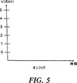
図5は、オンフック状態でのアンプ出力電圧対時間の簡単なグラフである。
好適な実施形態の詳細な説明
図1は、本発明のインターフェース回路10のある実施形態の簡単なブロック図である。回路10は、DDAの機能を実行することができ、そのため、コンピュータおよび/またはモデムのようなユーザ装置と、電話線12により、インターフェース回路10に接続している公衆電話網(PSTN)との間で、インターフェースとしての働きをする。回路10は、送信(Tx)モードおよび受信モードを供給し、送信モードの場合、信号は、ユーザ装置から電話線12に送られ、受信(Rx)モードの場合には、信号は電話線12からユーザ装置へ伝送される。
送信分離アンプは、第一のアンプ段14および第二のアンプ段16を含み、これらアンプ段は、光学的接続回路またはオプトカプラ18により、光学的に相互に分離され、また相互に接続している。ユーザ装置からの送信信号は、Txライン37に接続している第一のアンプ段14のところで受信され、第一のアンプ段14により増幅、または処理され、オプトカプラ18により第二のアンプ段16に送られる。第二のアンプ段16からの増幅された送信信号は、ハイブリッド・インターフェース回路20に送られる。上記ハイブリッド・インターフェース回路20は、2−4線式コンバータとして働き、フック・スイッチ制御ライン24によりオンになった場合、フック・スイッチ22を通して、送信信号を電話線12に送る。
2−4線式コンバータ20により、回路10およびユーザ装置は、標準2線チップおよびリング電話線12を使用する、送信/受信構成で動作することができる。送信モードおよび受信モードは、それぞれ、二本の線を使用し、2−4線式コンバータは、インターフェースの動作モードにより、送信回路および受信回路の間で二本の標準チップおよびリング電話線を切り換える。
アンプのプリバイアスは、ライン26を通して、オプトカプラ18により、アンプに送られる。制御ライン28上のオフフック/プリバイアス制御信号が作動すると、プリバイアスがアンプに送られる。さらに、オフフック/プリバイアス信号が作動すると、インターフェース回路10は、フック・スイッチ制御ライン24により、オフフック状態になる。フック・スイッチ制御ライン24が作動すると、フック・スイッチ22がオンになり、その結果、電流が、PSTNとユーザ装置との間の電話線12を流れることができる。それ故、分離アンプにプリバイアスを送るのにも、インターフェース回路10のフック状態、すなわち、フック・スイッチ22を制御するのにも、一本の制御ライン28が使用される。制御ライン28が作動していない場合には、分離アンプ回路にプリバイアスが掛からなくなり、フック・スイッチ22がオフになり、その結果、電流が電話線12へまた電話線12へ流れることができなくなる。
上記回路の受信部分は、プリバイアスおよびフック・スイッチ制御を除けば、送信部分に類似している。受信分離アンプは、光学的接続回路またはオプトカプラ34により、第二のアンプ段32に接続している第一のアンプ段30を含む。PSTNからの信号は、電話線12から、フック・スイッチ22および2−4線式コンバータ20を通して、ライン36に沿って受信回路に転送される。増幅された受信信号は、ライン38によりユーザ装置に伝送される。
図2は、本発明のインターフェース回路10のある実施形態のより詳細な略図である。本発明の分離アンプ回路は、抵抗R1、R2およびR3、アンプ50および58および光学的接続回路52を含み、上記光学的接続回路52は、LED53、および感光トランジスタまたはホトダイオード55および56含むことができる。分離アンプは、ユニポーラ光起電形アンプである。ライン37のところのTxターミナルに送られた入力信号は、通常、アース電位を挟んで上下に変動する二極正弦波形である。アンプは単端子電源VCCから電力の供給を受けているので、アースのところで信号がクリップするのを防止するために、プリバイアスがアンプに掛けられる。ライン82上の合成アンプ回路の出力電圧Vは、下記式により表わされる。
![]()
K3=K2/K1
ここで、K1はLED53を流れる電流の、ホトダイオード55が発生した電流に対する電流伝達比率であり、
K2は、LED53を流れる電流の、ホトダイオード56が発生する電流に対する電流伝達比率である。
入力信号V0は、アース電位を中心にして上下に変動するので、また単極の電源VCCを使用しているので、プリバイアスがアンプに掛けられ、その結果、ライン82のところのアンプの出力Vは、アース電位よりは上、VCCよりは下のレベルのところのDC静出力電圧VQに設定され、ライン37のところの入力信号は、単端子アンプ50によりクリップされない。VQは、通常、VCC/2に設定される。
この場合、送信信号がTxターミナルに掛かっていない場合には、すなわち、V0=0である場合で、全体の伝達利得K3=1と仮定した場合には、式1は下記式のように簡単になる。
![]()
この静出力電圧VQは、LED電流Ifを流すアンプ50の非反転ノードのところのノード91に注入される電流により発生する。その大きさがIfと同じである、結果として得られる光電流I1は、ノード91から流れだし、その結果、ノード91は、事実上アース電位に維持される。数式で表わせば、I1(If)(K1)となる。LED53の出力光線も、ホトダイオード56に当り、電流I2が、アンプ58の非反転ノードのところに流れる。その結果、82のところでの出力電圧V=(I2)(R3)となる。
それ故、オフフック/プリバイアス信号が作動すると(ロー)、トランジスタ54が電流Ifを流し、その結果、LED53が発光する。この光は、オプトカプラ52のところの反射ドームにより、ホトダイオード55および56に反射され、その結果、アンプ段50および58は、オプトカプラ52により接続され、ライン82のところに出力電圧Vが送られる。Tx入力に信号が入力していない場合には、プリバイアスが掛けられ、その結果、DC静電圧VQだけがライン82のところに現われる。しかし、送信信号が入力している場合には、ライン82のところの出力電圧Vは、式1に示すように変調される。
82のところの出力信号は、2−4線式コンバータの機能を果たす回路60に送られ、上記コンバータにより、本発明の回路の送信機能および受信機能を、2−4線式コンバータ60を通して、標準2線式PSTNに接続している4本のラインで実行することができる。送信信号は、ライン84を通して、フック・スイッチとして機能するペアのPNPダーリントン・トランジスタ62に送られる。ペアのダーリントン・トランジスタ62が、ライン86を通して、飽和状態に作動すると、その中を電流が流れ、ライン84上の出力信号が、ダイオード・ブリッジ回路64を通して、電話線12のチップおよびリング・ラインに送られる。
図2に示すように、本発明のある実施形態の場合には、ペアのダーリントン・トランジスタフック・スイッチ62は、制御ライン86を通して動作し、その状態は、光学的接続回路52のホトトランジスタ57を通って流れる電流により制御される。ホトトランジスタ57は、LED53およびホトダイオード55および56用の、同じ反射ドームの下に位置していて、そのため、LED53を流れる電流は、同時に三つのすべての装置55、56および57に送られる。すでに説明したとおり、オフフック/プリバイアス信号が作動(ロー)し、電流IfがLED53を通って流れると、アンプ段50および58は一緒に接続される。さらに、ホトトランジスタ57も、同時に作動し、その結果、ペアのダーリントン・トランジスタ62を通って電流が流れる。すなわち、フック・スイッチ62がオンになり、電流が電話線12を通して流れることができるようになる。回路66は、電話線からの電流が流れ易いように、低いDC抵抗および高いACインピーダンスを持つジャイレータ回路または電子インダクタである。
インターフェース装置10の受信回路は、抵抗R7およびR8、アンプ68および80、電源回路78および光学的接続回路70を含み、上記光学的接続回路70は、LED72およびホトダイオード74および76、および光学的反射ドームを含む。電話線12のチップおよびリング・ラインのところで受信した入力信号は、ダイオード・ブリッジ64により、ダーリントン・トランジスタフック・スイッチ62を通し、ライン84を経由して、2−4線式コンバータ60に送られる。回路60は、入力信号を受信回路に転送する。アンプ68の第一の増幅段が、電源78から電力の供給を受けているLED72を駆動する。回路78は、電話線12からの生の電力を使用して、受信回路に調整された電力を供給する。変調した入力信号は、ライン81に接続している受信回路に送られる。上記信号は、アンプ68および抵抗R8を通して、LED72の出力を変調する。入力信号は、反射ドームにより、光学的接続装置70を通してホトダイオード76に送られ、上記ホトダイオードは、この信号をアンプ80に送信する。処理された受信信号は、ライン38を通して、ユーザ装置またはモデムに送られ、処理される。
図3−図5は、本発明のインターフェース回路10の種々の動作状態を示す、電圧対時間のグラフである。このグラフは、VCC=5ボルト、K3=1の場合のものである。
図3は、Txに入力送信信号が存在しない状態、すなわち、V0=0の場合の、ライン82のところの電圧Vのグラフである。この図は、またインターフェース回路が、オフフック状態にある場合の状況も示す。この場合、ライン82のところの出力電圧Vは、V=VQ、静DC出力電圧である時間の間一定である。
図4Aは、Tx入力に掛けられた例示としての時変信号のグラフである。通常、入力信号は、V0の振幅を持つ二極信号である。すなわち、図4Aに示すように、信号電圧は、時間の経過とともに、正の値(0ボルト以上)と負の値(0ボルト以下)との間を変動する。
図4Bは、本発明のインターフェース回路が、オフフック状態であり、V0のピーク電圧を持つ図4Aの二極信号が、Tx入力に掛けられている状態を示す。ライン82のところの電圧Vは、VQのバイアスDC値程度変化する時変信号である。
図5は、システムがオンフック状態、すなわち、オフフック/プリバイアス信号が作動していないで(ハイ)の状態で、そのため、電流IfがLED53を通って流れていない状態での、ライン82のところの電圧Vである。この状態の場合、アンプ段50および58は、相互に分離され、プリバイアスは回路に掛かっていない。その結果、ライン82のところの信号Vは、0ボルトの一定のレベルである。
好適な実施形態を参照しながら、本発明を詳細に図示し、説明してきたが、当業者なら、下記の請求の範囲に記載する、本発明の精神および範囲から逸脱することなしに、形式および詳細な点を種々に変更することができることを理解することができるだろう。Background of the Invention Telephone interface devices such as modems are typically used to connect telephone lines to user devices such as computers. Generally speaking, these devices typically include a device interface for connecting to a computer and a telephone line interface for connecting to a telephone line. A telephone line interface typically includes a type of circuit commonly referred to as a data access device (DAA). This circuit sends and receives various telephone line signals, otherwise it acts as a telephone line interface that is normally required.
The circuitry of the interface device may include a separation amplifier circuit that receives a signal from a computer and sends the signal to the telephone line while separating between the user equipment and the telephone line. The amplifier circuit may include first and second amplification stages that are optically isolated from each other while being optically connected to each other. In the normal method, the first stage of the amplifier drives a light emitting element such as a light emitting diode (LED) that is optically connected to a photosensitive element such as a photodiode of the second amplifier stage. In order to make an optical connection, a reflective dome is usually placed over the LED and photodiode.
Usually, the signal sent from the user device to the first amplifier stage is a bipolar signal. That is, a signal whose level fluctuates between a positive voltage and a negative voltage. In order to allow the separation amplifier to receive a bipolar signal without causing clipping, the interface device usually increases the DC level of the amplifier so that it can process the bipolar input signal. And a pre-bias circuit for continuously applying a DC pre-bias to the amplifier.
The interface device is also adapted to connect to the telephone line in an “off-hook” state so that current can flow between the public telephone network (PSTN) and the user equipment. A switching circuit called a “hook switch” can be included. In the “on hook” state, the hook switch is turned off to prevent current from flowing through the PSTN. A conventional hook switch circuit includes a relay that is controlled by a user device by a control signal. When activated, the signal turns on the relay to connect to the telephone line, otherwise it turns off the relay.
In some conventional systems, the hook switch control signal is optically separated from the hook switch itself. The control signal activates a light emitting element, such as an LED, optically connected to the photosensitive device, such as a phototransistor or photodiode. When the hook switch signal is activated, the photodiode goes off-hook to turn on the hook switch and thereby connect to the telephone line.
Clause U.S. Pat. No. 5,555,293 discloses a DAA telephone interface device having a conventional prior art interface configuration. The DAA disclosed in the above patent 293 includes a separation amplifier that is optically connected to a plurality of stages used to transmit signals between the telephone line and the subscriber unit. The apparatus also includes a separate hook switch circuit driven by an off-hook control line. The off-hook controller is optically connected to a hook switch circuit that includes a set of FET devices. Therefore, the above U.S. patent discloses a prior art system that uses individual and separate circuits for line signal separation / amplification and hook switch control.
Thus, prior art telephone interface devices such as, for example, DAA include a number of circuits to perform and control interface functions between user devices such as modems, computers, and the telephone network. Such hardware-focused systems can be very expensive, so reducing the number of electronic components in such systems is important to reduce overall size and cost. It can be said that there is.
The present invention relates to an interface circuit and method that serves as an interface between a telephone line and a user device such as a modem and / or a host computer. The circuit of the present invention includes a separation amplifier circuit for connecting a user telephone device and a telephone line and exchanging signals between the telephone device and the telephone line. A biasing means is connected to the amplifier circuit to bias or pre-bias the amplifier circuit so that bipolar signal variations can be processed. The bias means can be switched so as to be able to switch between a bias state in which the amplifier circuit is pre-biased and a non-bias state in which the amplifier circuit is not pre-biased. The interface circuit also includes a hook switch circuit that controls the connection of the telephone device to the telephone line. The hook switch can switch between a connected state where current can flow between the telephone device and the telephone line and a disconnected state where current cannot flow. The interface circuit also biases the hook switch circuit so that when the biasing means is switched between a biased state and an unbiased state, the hook switch switches between a connected state and an unconnected state. Means for connecting. Therefore, the present invention provides a telephone interface circuit in which controlling the hook switch controls the pre-bias for the amplifier and / or controlling the pre-bias for the amplifier also controls the hook switch.
In some embodiments, the isolation amplifier circuit includes a first amplifier stage and a second amplifier that are optically interconnected to provide the necessary DC isolation between the telephone line and the user telephone device. Includes an amplifier stage. The optical connecting device includes a light emitting element such as an LED under a reflective element such as a reflective dome. As current flows through the LED, the reflective dome directs light to a first photosensitive device, such as a phototransistor or photodiode, and the first amplifier stage and the second amplifier stage connected to the second amplifier stage. Sent to the second photosensitive device. The current flowing through the LED also applies a DC bias to the amplifier to handle the bipolar nature of the signal being sent to the telephone line. The current flowing through the LED is controlled by a control signal sent to a switch such as a transistor so that the pre-bias and the connection of the first and second amplifier stages can be controlled externally.
In some embodiments, the hook switch circuit is a photodiode or phototransistor, such as a photodiode or phototransistor, installed near the same optical reflective element used to connect the first and second amplifier stages. Includes a photosensitive device. When the pre-bias signal is activated to pre-bias the amplifier, light is sent from the LED to the photosensitive device of the hook switch circuit. The hook switch is turned on so that current flows through the telephone line. Therefore, since the control signal used to operate the pre-bias switch is also in the off-hook state, when the hook switch is turned on, the pre-bias is also applied to the amplifier circuit. Make it work.
The interface circuit of the present invention performs the pre-bias operation and the hook switch function in a single operation. In some embodiments, this operation is accomplished by forming a plurality of optically connected circuits under the same optical reflective dome. More specifically, in one embodiment, the photosensitive device for the first and second amplifier stages, and the hook switch circuit and LED are all formed under the same optical reflective dome.
The telephone interface circuit and method of the present invention has many advantages compared to conventional approaches. For example, by combining the pre-bias function of the amplifier and the hook switch function, the present invention reduces circuit space and cost. One optical isolation / connection device is used to optically isolate / connect multiple amplifier stages and hook switch control circuits. The use of a single optical connection device instead of multiple devices previously used reduces circuit space and cost, which is crucial in the competitive wireless communications hardware industry. That is.
Also, by using a switching pre-bias, the overall power consumption of the interface circuit is significantly reduced. Therefore, the interface is pre-biased and consumes power only while the interface is in use off-hook. In the case of the conventional system, the pre-bias is continuously applied, and as a result, power is wasted at any time.
[Brief description of the drawings]
These and other objects and features and advantages of the present invention will be understood upon reading of a more detailed description of the preferred embodiment of the present invention shown in the accompanying drawings. Like reference numerals refer to like parts throughout the drawings. The scale of the drawings is not necessarily accurate, but focuses on explaining the principles of the invention.
FIG. 1 is a block diagram of an embodiment of an interface circuit of the present invention.
FIG. 2 is a detailed schematic diagram of the interface circuit of FIG.
FIG. 3 is a simple graph of amplifier output voltage versus time in the off-hook state where no transmission signal is present.
FIG. 4A is a simplified diagram of an exemplary bipolar voltage signal sent to the circuit of the present invention.
FIG. 4B is a simple graph of amplifier output voltage versus time in an off-hook state when the transmission signal of FIG. 4A is applied to the amplifier.
FIG. 5 is a simple graph of amplifier output voltage versus time in the on-hook state.
Detailed Description of the Preferred Embodiment FIG. 1 is a simplified block diagram of one embodiment of an
The transmission separation amplifier includes a
The 2-4
The pre-bias of the amplifier is sent to the amplifier through line 26 by
The receive portion of the circuit is similar to the transmit portion except for pre-bias and hook switch control. The receive separation amplifier includes a
FIG. 2 is a more detailed schematic diagram of an embodiment of the
![]()
K3 = K2 / K1
Here, K1 is a current transmission ratio of the current flowing through the LED 53 to the current generated by the photodiode 55,
K2 is a current transmission ratio of the current flowing through the LED 53 to the current generated by the photodiode 56.
Since the input signal V 0 fluctuates up and down around the ground potential, and since a single-pole power supply V CC is used, a pre-bias is applied to the amplifier, and as a result, the amplifier at
In this case, when the transmission signal is not applied to the Tx terminal, that is, when V 0 = 0, and assuming that the entire transmission gain K3 = 1,
![]()
This static output voltage V Q is generated by the current injected into the
Therefore, when the off-hook / pre-bias signal is activated (low), transistor 54 conducts current If and, as a result, LED 53 emits light. This light is reflected by the reflection dome at the
The output signal at 82 is sent to a
As shown in FIG. 2, in one embodiment of the present invention, a pair of Darlington transistor hook switches 62 operate through a
The receiving circuit of the
3-5 are voltage versus time graphs illustrating various operating states of the
FIG. 3 is a graph of the voltage V at
FIG. 4A is a graph of an exemplary time-varying signal multiplied by a Tx input. Usually, the input signal is a bipolar signal having an amplitude of V 0 . That is, as shown in FIG. 4A, the signal voltage fluctuates between a positive value (0 volts or more) and a negative value (0 volts or less) with the passage of time.
FIG. 4B shows a state in which the interface circuit of the present invention is in an off-hook state and the bipolar signal of FIG. 4A having a peak voltage of V 0 is applied to the Tx input. Voltage V at the
FIG. 5 shows at
While the invention has been illustrated and described in detail with reference to a preferred embodiment, those skilled in the art will recognize the form and form described in the following claims without departing from the spirit and scope of the invention. It will be understood that the details can be varied in various ways.
Claims (18)
前記電話装置と電話線の間に接続され、前記電話装置と前記電話線との間で信号を供給するためのアンプ回路と、
前記アンプ回路に提供され前記アンプ回路が、二極信号を処理することができるように、前記アンプ回路にバイアスを掛けるためのバイアス手段であって、バイアス状態と、非バイアス状態の間を切り換わることのできるバイアス手段と、
前記電話線への前記電話回路の接続を制御するためのフック・スイッチ回路であって、接続状態と非接続状態との間を切り換わることのできるフック・スイッチ回路と、
前記バイアス手段が、前記バイアス状態と前記非バイアス状態との間を切り換わるにつれて、前記フック・スイッチが、前記接続状態と、前記非接続状態との間を切り換わるように、前記バイアス手段を前記フック・スイッチ回路に接続するための手段と、を備えるインターフェース回路。An interface circuit for providing an interface to between the telephone device and the telephone line,
An amplifier circuit for supplying a signal to and from the connected between the telephone device and the telephone line, the telephone line and the telephone device,
The amplifier circuit is provided wherein the amplifier circuit is, to be able to handle bipolar signals, a biasing means for biasing said amplifier circuit, conversion cut and biased, between the non-bias state and bias means that can I Rukoto,
A hook switch circuit for controlling the connection of said telephone circuit to said telephone line, and a hook switch circuit capable of conversion I Rukoto off between the connected state and the disconnected state,
Said biasing means, as Waru switch the between the non-bias state and the bias state, the hook switch is, with the connection state, to so that I switch the between the non-connected state, the bias interface circuit and means for connecting the unit to the hook switch circuit.
第一のアンプ段と、
第二のアンプ段と、
アンプ回路に接続され、前記アンプ回路が、二極信号を処理することができるように、前記アンプ回路にバイアスを掛けるためのバイアス手段であって、バイアス状態と非バイアス状態との間を切り換えることができるバイアス手段と、
切り換え可能な信号出力を提供するための切り換え可能な信号出力回路であって、前記バイアス手段が前記バイアス状態と非バイアス状態との間を切り換わるにつれて、切り換え可能な信号出力が、第一の状態と第二の状態との間で切り換わるように、前記バイアス手段に接続されている切り換え可能な信号出力回路と、
前記第一のアンプ段を前記第二のアンプ段に光学的に接続するためのものであって、前記バイアス手段を前記切り換え可能な信号出力回路に光学的に接続している光学的接続手段とを備える分離アンプ。A separation amplifier,
The first amplifier stage,
A second amplifier stage,
Connected to the amplifier circuit, the amplifier circuit, to be able to handle bipolar signals, a biasing means for biasing said amplifier circuit, to switch between the bias state and non bias state Bias means that can
A switchable signal output circuit order to provide a switchable signal output, as the biasing means Waru switch the between the bias state and non bias state, switchable signal output, the first A switchable signal output circuit connected to the biasing means to switch between a state and a second state;
Optical connection means for optically connecting the first amplifier stage to the second amplifier stage, and optically connecting the bias means to the switchable signal output circuit; Separate amplifier with.
発光を反射するための光学的反射素子と、
前記光学的反射素子からの反射発光を、受光するための複数の感光装置であって、前記感光装置の中の一方が、前記フック・スイッチ回路に接続していて、前記感光装置の他方が、前記第一および第二のアンプ段の中の一つに接続している複数の感光装置とを備える分離アンプ。14. The separation amplifier according to claim 13, wherein the optical connecting means is
An optical reflective element for reflecting light emission;
A plurality of photosensitive devices for receiving reflected light from the optical reflecting element, wherein one of the photosensitive devices is connected to the hook switch circuit, and the other of the photosensitive devices is A separation amplifier comprising a plurality of photosensitive devices connected to one of the first and second amplifier stages;
前記電話装置と前記電話線との間で信号を結合するために、前記電話装置と前記電話線との間にアンプ回路を接続するステップと、
前記アンプ回路が二極信号を処理することができるように、前記アンプ回路にバイアスを掛けるための、前記アンプ回路にバイアス回路を接続するステップであって、前記バイアス回路がバイアス状態と非バイアス状態との間を切り換わることが可能となっているステップと、
前記電話線への前記電話装置の接続を制御するためのフック・スイッチ回路を提供するステップであって、前記フック・スイッチが、接続状態と非接続状態との間を切り換えることが可能となっているステップと、
前記バイアス回路が前記バイアス状態と前記非バイアス状態との間で切り換わるにつれて、前記フック・スイッチ回路が前記接続状態と前記非接続状態との間を切り換わるように、前記フック・スイッチに前記バイアス回路を接続するステップと含む方法。A method subjecting Hisage an interface between the telephone line and the telephone device,
Connecting an amplifier circuit between the telephone device and the telephone line to couple a signal between the telephone device and the telephone line;
As can be said amplifier circuit to process a bipolar signal, the amplifier circuit for biasing the, a step of connecting the bias circuit to the amplifier circuit, the bias circuit is biased and non-biased state a step that is the possible conversion I Rukoto off between,
Providing a hook switch circuit for controlling connection of the telephone device to the telephone line, the hook switch being able to switch between a connected state and a disconnected state. And steps
As the bias circuit that button switches the mode between the non-bias state and the bias condition, in so that I switch the between the hook switch circuit the non-connected state to the connected state, the hook Connecting the bias circuit to a switch.
Applications Claiming Priority (3)
| Application Number | Priority Date | Filing Date | Title |
|---|---|---|---|
| US08/873,674 | 1997-06-12 | ||
| US08/873,674 US5946394A (en) | 1997-06-12 | 1997-06-12 | Isolation amplifier with hook switch control |
| PCT/US1998/012269 WO1998057476A1 (en) | 1997-06-12 | 1998-06-12 | Isolation amplifier with hook switch control |
Publications (3)
| Publication Number | Publication Date |
|---|---|
| JP2002504287A JP2002504287A (en) | 2002-02-05 |
| JP2002504287A5 JP2002504287A5 (en) | 2005-12-22 |
| JP4564109B2 true JP4564109B2 (en) | 2010-10-20 |
Family
ID=25362110
Family Applications (1)
| Application Number | Title | Priority Date | Filing Date |
|---|---|---|---|
| JP50326299A Expired - Fee Related JP4564109B2 (en) | 1997-06-12 | 1998-06-12 | Separate amplifier including hook switch controller |
Country Status (6)
| Country | Link |
|---|---|
| US (1) | US5946394A (en) |
| EP (1) | EP1002411B1 (en) |
| JP (1) | JP4564109B2 (en) |
| AU (1) | AU7838498A (en) |
| TW (1) | TW380348B (en) |
| WO (1) | WO1998057476A1 (en) |
Families Citing this family (18)
| Publication number | Priority date | Publication date | Assignee | Title |
|---|---|---|---|---|
| US6192125B1 (en) * | 1998-07-01 | 2001-02-20 | Texas Instruments Incorporated | Optical coupling circuit for a data access arrangement (DAA) |
| US6681012B1 (en) * | 1999-09-23 | 2004-01-20 | Nortel Networks Limited | Directional receiver coupling arrangement with frequency selectivity and gain control for DSL |
| US6376933B1 (en) | 1999-12-31 | 2002-04-23 | Honeywell International Inc. | Magneto-resistive signal isolator |
| US7110525B1 (en) | 2001-06-25 | 2006-09-19 | Toby Heller | Agent training sensitive call routing system |
| JP4503890B2 (en) | 2001-08-06 | 2010-07-14 | 株式会社リコー | Facsimile machine |
| US7139391B2 (en) * | 2001-10-30 | 2006-11-21 | Integration Associates, Inc. | DAA hook switch |
| JP2003234623A (en) * | 2002-02-12 | 2003-08-22 | Sharp Corp | Light receiving amplifier circuit and optical pickup using the same |
| US7372952B1 (en) | 2002-03-07 | 2008-05-13 | Wai Wu | Telephony control system with intelligent call routing |
| US7277491B2 (en) * | 2002-05-14 | 2007-10-02 | Ess Technology, Inc. | Data access arrangement using a high frequency transformer for electrical isolation |
| US7103175B2 (en) * | 2003-01-08 | 2006-09-05 | Vtech Telecommunications Limited | Systems and methods for an electronic hook switch for customer premises equipment |
| US9818136B1 (en) | 2003-02-05 | 2017-11-14 | Steven M. Hoffberg | System and method for determining contingent relevance |
| EP1447961A1 (en) * | 2003-02-12 | 2004-08-18 | Integration Associates Inc. | Hook switch circuit and power circuit for electronic telephone line interface |
| US7676034B1 (en) | 2003-03-07 | 2010-03-09 | Wai Wu | Method and system for matching entities in an auction |
| US8874477B2 (en) | 2005-10-04 | 2014-10-28 | Steven Mark Hoffberg | Multifactorial optimization system and method |
| US8300798B1 (en) | 2006-04-03 | 2012-10-30 | Wai Wu | Intelligent communication routing system and method |
| US10191220B2 (en) * | 2012-12-21 | 2019-01-29 | Volcano Corporation | Power-efficient optical circuit |
| US9088282B2 (en) * | 2013-01-25 | 2015-07-21 | Apple Inc. | Proximity sensors with optical and electrical sensing capabilities |
| AU2015343339A1 (en) | 2014-11-03 | 2017-06-15 | Genentech, Inc. | Methods and biomarkers for predicting efficacy and evaluation of an OX40 agonist treatment |
Family Cites Families (28)
| Publication number | Priority date | Publication date | Assignee | Title |
|---|---|---|---|---|
| US3772514A (en) * | 1971-11-08 | 1973-11-13 | Capintec Inc | Isolation amplifier |
| US4137428A (en) * | 1977-10-27 | 1979-01-30 | Bell Telephone Laboratories, Incorporated | Optically actuated bidirectional semiconductor switch |
| JPS5555655A (en) * | 1978-10-20 | 1980-04-23 | Nippon Telegr & Teleph Corp <Ntt> | Selection unit for telephone line |
| US4282604A (en) * | 1979-04-04 | 1981-08-04 | Jefferson William T | Optical isolation circuit for bidirectional communication lines |
| US4310725A (en) * | 1980-01-17 | 1982-01-12 | Solid State Systems, Inc. | Interface for private branch exchange |
| US4317964A (en) * | 1980-07-30 | 1982-03-02 | Bell Telephone Laboratories, Incorporated | Off-hook/on-hook status check circuit |
| FR2548494B1 (en) * | 1983-06-30 | 1985-10-31 | Horlogerie Photograph Fse | COMPUTER TELEPHONE-TERMINAL ASSEMBLY WITH SINGLE DECIMAL KEYBOARD AND LOCAL SWITCHABLE POWER |
| US4558183A (en) * | 1983-10-03 | 1985-12-10 | Cellutron Corporation | Opto-coupler interfacing circuit |
| US4591663A (en) * | 1983-11-17 | 1986-05-27 | Trad, Inc. | Servo-linearized opto-electronic analog interface |
| USH118H (en) * | 1984-10-11 | 1986-09-02 | At&T Bell Laboratories | Synthesized sound telephone alerting means |
| US4727535A (en) * | 1985-04-08 | 1988-02-23 | Rapitech System Inc. | Telephone network coupler |
| US4723267A (en) * | 1985-06-17 | 1988-02-02 | Octocom Systems, Inc. | Telephone line interface and dialer circuitry for telecommunications equipment |
| US4742538A (en) * | 1985-07-05 | 1988-05-03 | Melita Electronic Labs, Inc. | Current source and off-hook detector |
| US4860345A (en) * | 1986-12-22 | 1989-08-22 | Protel, Inc. | Telephone system and method operated from central office loop current |
| AU618651B2 (en) * | 1989-02-02 | 1992-01-02 | Alcatel Australia Limited | Battery boosted dial memory |
| US5291545A (en) * | 1990-10-02 | 1994-03-01 | Intertex Data Ab | Apparatus and method for determining the state of a telephone line |
| GB9102290D0 (en) * | 1991-02-02 | 1991-03-20 | Mixalloy Ltd | Production of flat products |
| US5245654A (en) * | 1991-10-10 | 1993-09-14 | Cermetek Microelectronics, Inc. | Solid state isolation device using opto-isolators |
| US5280526C1 (en) * | 1992-05-26 | 2001-05-01 | Paradyne Corp | Transformer-less hybrid circuit |
| US5369687A (en) * | 1992-12-17 | 1994-11-29 | Practical Peripherals, Inc. | Apparatus for electrically isolating a telephone line from a data device |
| US5734703A (en) * | 1993-05-26 | 1998-03-31 | Hitachi Maxell, Ltd. | Hybrid circuit and data communication apparatus |
| DE69421884T2 (en) * | 1993-09-30 | 2000-05-11 | Siemens Comp Inc | Linear bidirectional optocoupler |
| US5438210A (en) * | 1993-10-22 | 1995-08-01 | Worley; Eugene R. | Optical isolation connections using integrated circuit techniques |
| EP0651541B1 (en) * | 1993-10-29 | 2001-01-10 | STMicroelectronics S.r.l. | Telephone subscriber circuit with galvanic isolating element for driving the on/off states of a telephone line |
| DE19503164A1 (en) * | 1994-02-04 | 1995-08-10 | Siemens Comp Inc | Optically coupled data switching system and handset cradle switch |
| WO1996005686A1 (en) * | 1994-08-10 | 1996-02-22 | Cp Clare Corporation | Bilateral switch for modem applications |
| US5751803A (en) * | 1995-11-08 | 1998-05-12 | Shmuel Hershkovit | Telephone line coupler |
| US5600715A (en) * | 1996-02-28 | 1997-02-04 | Lucent Technologies Inc. | Integrated loop current detector apparatus for a PSTN modem |
-
1997
- 1997-06-12 US US08/873,674 patent/US5946394A/en not_active Expired - Lifetime
-
1998
- 1998-06-12 JP JP50326299A patent/JP4564109B2/en not_active Expired - Fee Related
- 1998-06-12 AU AU78384/98A patent/AU7838498A/en not_active Abandoned
- 1998-06-12 TW TW087109368A patent/TW380348B/en not_active IP Right Cessation
- 1998-06-12 WO PCT/US1998/012269 patent/WO1998057476A1/en active Application Filing
- 1998-06-12 EP EP98926583.0A patent/EP1002411B1/en not_active Expired - Lifetime
Also Published As
| Publication number | Publication date |
|---|---|
| US5946394A (en) | 1999-08-31 |
| AU7838498A (en) | 1998-12-30 |
| EP1002411B1 (en) | 2013-10-23 |
| JP2002504287A (en) | 2002-02-05 |
| TW380348B (en) | 2000-01-21 |
| EP1002411A1 (en) | 2000-05-24 |
| EP1002411A4 (en) | 2010-07-21 |
| WO1998057476A8 (en) | 1999-04-15 |
| WO1998057476A1 (en) | 1998-12-17 |
Similar Documents
| Publication | Publication Date | Title |
|---|---|---|
| JP4564109B2 (en) | Separate amplifier including hook switch controller | |
| US5280526A (en) | Transformer-less hybrid circuit | |
| US5946393A (en) | Data access arrangement | |
| US4893331A (en) | System allowing selective connection of various types of external apparatuses to telephone set | |
| US5579144A (en) | Data access arrangement having improved transmit-receive separation | |
| US5528686A (en) | Transformerless hybrid circuit having direct powered line-side amplifiers | |
| US6211719B1 (en) | Power control circuit for a line driver | |
| US6192125B1 (en) | Optical coupling circuit for a data access arrangement (DAA) | |
| US6272220B1 (en) | Electronically switched optically coupled line interface | |
| JPH0851496A (en) | Hybrid circuit and modem containing no transformer | |
| US4727535A (en) | Telephone network coupler | |
| US6757381B1 (en) | Design of telephone line interface circuits using a two chip opto-coupler with LEDs integrated onto silicon chips | |
| US4953200A (en) | Private branch exchange capable of discriminating different types of telephone sets connected thereto | |
| US6377681B1 (en) | Signal line driving circuit with self-controlled power dissipation | |
| GB2106755A (en) | Detector circuit for communication lines | |
| WO1988006386A1 (en) | Telephone network coupler | |
| US6353347B1 (en) | Power control circuit for a line driver | |
| EP1533985B1 (en) | Direct access arrangement | |
| EP0651540B1 (en) | Telephone subscriber circuit with galvanic isolating element | |
| JPH046281Y2 (en) | ||
| US5466944A (en) | Optically-coupled differential line receiver | |
| JP3005438B2 (en) | Speech network circuit | |
| KR950002583B1 (en) | Key-phone system | |
| EP1447961A1 (en) | Hook switch circuit and power circuit for electronic telephone line interface | |
| WO1996002103A1 (en) | A telephone interface circuit |
Legal Events
| Date | Code | Title | Description |
|---|---|---|---|
| A521 | Request for written amendment filed |
Free format text: JAPANESE INTERMEDIATE CODE: A523 Effective date: 20050610 |
|
| A621 | Written request for application examination |
Free format text: JAPANESE INTERMEDIATE CODE: A621 Effective date: 20050610 |
|
| RD04 | Notification of resignation of power of attorney |
Free format text: JAPANESE INTERMEDIATE CODE: A7424 Effective date: 20050610 |
|
| A977 | Report on retrieval |
Free format text: JAPANESE INTERMEDIATE CODE: A971007 Effective date: 20071005 |
|
| A131 | Notification of reasons for refusal |
Free format text: JAPANESE INTERMEDIATE CODE: A131 Effective date: 20081021 |
|
| A601 | Written request for extension of time |
Free format text: JAPANESE INTERMEDIATE CODE: A601 Effective date: 20090120 |
|
| A602 | Written permission of extension of time |
Free format text: JAPANESE INTERMEDIATE CODE: A602 Effective date: 20090302 |
|
| TRDD | Decision of grant or rejection written | ||
| A01 | Written decision to grant a patent or to grant a registration (utility model) |
Free format text: JAPANESE INTERMEDIATE CODE: A01 Effective date: 20100706 |
|
| A01 | Written decision to grant a patent or to grant a registration (utility model) |
Free format text: JAPANESE INTERMEDIATE CODE: A01 |
|
| A61 | First payment of annual fees (during grant procedure) |
Free format text: JAPANESE INTERMEDIATE CODE: A61 Effective date: 20100730 |
|
| FPAY | Renewal fee payment (event date is renewal date of database) |
Free format text: PAYMENT UNTIL: 20130806 Year of fee payment: 3 |
|
| R150 | Certificate of patent or registration of utility model |
Free format text: JAPANESE INTERMEDIATE CODE: R150 |
|
| R250 | Receipt of annual fees |
Free format text: JAPANESE INTERMEDIATE CODE: R250 |
|
| R250 | Receipt of annual fees |
Free format text: JAPANESE INTERMEDIATE CODE: R250 |
|
| R250 | Receipt of annual fees |
Free format text: JAPANESE INTERMEDIATE CODE: R250 |
|
| R250 | Receipt of annual fees |
Free format text: JAPANESE INTERMEDIATE CODE: R250 |
|
| LAPS | Cancellation because of no payment of annual fees |