JP4562919B2 - Method and apparatus for implementing dynamic display memory - Google Patents
Method and apparatus for implementing dynamic display memory Download PDFInfo
- Publication number
- JP4562919B2 JP4562919B2 JP2000594101A JP2000594101A JP4562919B2 JP 4562919 B2 JP4562919 B2 JP 4562919B2 JP 2000594101 A JP2000594101 A JP 2000594101A JP 2000594101 A JP2000594101 A JP 2000594101A JP 4562919 B2 JP4562919 B2 JP 4562919B2
- Authority
- JP
- Japan
- Prior art keywords
- memory
- graphics
- operand
- control component
- address
- Prior art date
- Legal status (The legal status is an assumption and is not a legal conclusion. Google has not performed a legal analysis and makes no representation as to the accuracy of the status listed.)
- Expired - Fee Related
Links
Images


Classifications
-
- G—PHYSICS
- G09—EDUCATION; CRYPTOGRAPHY; DISPLAY; ADVERTISING; SEALS
- G09G—ARRANGEMENTS OR CIRCUITS FOR CONTROL OF INDICATING DEVICES USING STATIC MEANS TO PRESENT VARIABLE INFORMATION
- G09G5/00—Control arrangements or circuits for visual indicators common to cathode-ray tube indicators and other visual indicators
- G09G5/36—Control arrangements or circuits for visual indicators common to cathode-ray tube indicators and other visual indicators characterised by the display of a graphic pattern, e.g. using an all-points-addressable [APA] memory
- G09G5/363—Graphics controllers
-
- G—PHYSICS
- G09—EDUCATION; CRYPTOGRAPHY; DISPLAY; ADVERTISING; SEALS
- G09G—ARRANGEMENTS OR CIRCUITS FOR CONTROL OF INDICATING DEVICES USING STATIC MEANS TO PRESENT VARIABLE INFORMATION
- G09G5/00—Control arrangements or circuits for visual indicators common to cathode-ray tube indicators and other visual indicators
- G09G5/36—Control arrangements or circuits for visual indicators common to cathode-ray tube indicators and other visual indicators characterised by the display of a graphic pattern, e.g. using an all-points-addressable [APA] memory
- G09G5/39—Control of the bit-mapped memory
- G09G5/393—Arrangements for updating the contents of the bit-mapped memory
-
- G—PHYSICS
- G09—EDUCATION; CRYPTOGRAPHY; DISPLAY; ADVERTISING; SEALS
- G09G—ARRANGEMENTS OR CIRCUITS FOR CONTROL OF INDICATING DEVICES USING STATIC MEANS TO PRESENT VARIABLE INFORMATION
- G09G2360/00—Aspects of the architecture of display systems
- G09G2360/12—Frame memory handling
- G09G2360/122—Tiling
Landscapes
- Engineering & Computer Science (AREA)
- Physics & Mathematics (AREA)
- Computer Hardware Design (AREA)
- General Physics & Mathematics (AREA)
- Theoretical Computer Science (AREA)
- Computer Graphics (AREA)
- Memory System Of A Hierarchy Structure (AREA)
- Image Input (AREA)
- Image Processing (AREA)
Description
【0001】
(発明の分野)
本発明は、グラフィックスのチップセットに関し、より具体的に述べれば、グラフィックス・メモリのマネジメントに関する。
【0002】
(関連技術の説明)
一般に、自身のメモリを制御することができるグラフィックス・サブシステムを備えることはよく知られており、この種のサブシステムは、通常、システムバスによって、CPU、メインメモリ、およびその他のデバイス、たとえば補助記憶デバイス等に接続される。この種のシステムバスは、CPU、メインメモリ、およびその他のデバイスに接続される。これによりCPUは、バスに接続されているあらゆるものにアクセスすることができる。グラフィックス・サブシステムは、しばしば、当該グラフィックス・サブシステムからのみアクセス可能な高速メモリを含んでいる。それに加えて、通常はシステムバスを介して、この種のサブシステムがメインメモリ内のオペランドにアクセスすることもある。
【0003】
こういったシステムにおいては、CPUが、グラフィックス・オペランドに対するオペレーションを実行しなければならないことも少なくない。しかしながら、これらのオペランドのオーガナイゼーションは、グラフィックス・サブシステムによって制御される。そのため、CPUがグラフィックス・サブシステムからオペランドを獲得することが必要になる。これに対して、CPUまたは関連するメモリ・マネジメント・ユニット(MMU)がグラフィックス・オペランドのオーガナイゼーションを制御することがあり、その場合にはグラフィックス・サブシステムが、そのオペレーションのためにCPUまたはMMUからデータを獲得しなければならなくなる。いずれの場合においても、一方のデバイスが、そのタスクを実行するために他方のデバイスに対してデータを要求しなければならないことから、ある程度の効率の低下が招かれる。
【0004】
別のシステムにおいては、CPUとグラフィックス・サブシステムが、ともにグラフィックス・オペランドのオーガナイゼーションを制御する。この種のシステムにおいては、CPUおよびグラフィックス・サブシステムが、互いにオペランドを要求する必要がなくなるが、メモリ内においてグラフィックス・オペランドの移動があった時点で互いの情報の交換が必要となり、それが行われない場合にはアクセス不能となる。その結果、グラフィックス・オペランドに対する各オペレーションに、オーバーヘッドの増加がもたらされる。
【0005】
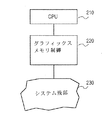
図1は、従来技術のシステムを示している。この図を参照すると、グラフィックス・アドレス変換器100(GAT 100)がグラフィックス・デバイス・コントローラ120(GDC 120)に接続されており、さらにそれがグラフィックス・デバイス130に接続されている。またGAT 100は、バスに接続されており、それによってメインメモリ160、補助記憶170、メモリ・マネジメント・ユニット150(MMU 150)に接続されている。中央処理ユニット140(CPU 140)は、MMU 150に接続されており、それによってメインメモリ160および補助記憶170にアクセスする。またCPU 140は、GAT 100に対する制御接続を有し、それによってCPU 140によるGAT 100の制御が可能になる。メインメモリ160は、セグメント・バッファ110を包含している。
【0006】
CPU 140は、メインメモリ160ならびに補助記憶170内に記憶されているグラフィックス・オペランドに対するオペレーションを行う。これを容易にするために、MMU 150は、各種オペランドがどこに記憶されているかについてのレコードを維持しつつ、メインメモリ160および補助記憶170をマネージする。メモリ内においてオペランドが移動させられると、MMU 150は、そのオペランドのロケーションのレコードを更新する。GDC 120もまた、メインメモリ160ならびに補助記憶170内に記憶されているグラフィックス・オペランドに対するオペレーションを行う。これを容易にするために、GAT 100は、グラフィックス・オペランドがどこに記憶されているかについてのレコードを維持しており、メモリ内においてオペランドの移動があったときには、それらのレコードを更新する。その結果、CPU 140もしくはGDC 120が、グラフィックス・オペランドの移動をもたらすアクションを行った場合には、必ずMMU 150ならびにGAT 100双方のレコードが更新されなければならないことになる。MMU 150およびGAT 100のレコードの間の一貫性を維持することは、メインメモリ160もしくは補助記憶170のいずれに対するアクセスにおいても多くのエラーに遭遇する可能性があることから、高度に同期化されたオペレーションを必要とする。
【0007】
たとえば、CPU 140が、補助記憶170からメモリのセグメントをメインメモリ160内のセグメント・バッファ110に移動し、それによってセグメント・バッファ110内の以前の内容を上書きすることがある。その種のアクションが発生したとき、MMU 150は、そのレコードを更新して、セグメント・バッファ110内にはどのようなオペランドがあり、どのオペランドがセグメント・バッファ110から削除されたかを継続的に追跡する。これらのオペランドのうちのいずれかがグラフィックス・オペランドである場合には、CPU 140がGAT 100をその制御の下に置いて、GAT 100に対して、関連する各種グラフィックス・オペランドに関するレコードを更新させる。さらに、CPU 140がセグメント・バッファ110を上書きしたとき、GDC 120がセグメント・バッファ110にアクセスしていると、GDC 120は壊れたデータもしくは正しくないデータに対してオペレーションを行うことになる。
【0008】
(発明の要約)
本発明は、ダイナミック・ディスプレイ・メモリを実装するための方法および装置である。本発明の一実施態様は、中央処理ユニットとメモリの間の仲裁に適したメモリ制御ハブである。このメモリ制御ハブは、グラフィックス・メモリ制御コンポーネントおよびメモリ制御コンポーネントを包含している。
【0009】
添付図面には、限定の意図ではなく例示を目的として本発明を示した。
【0010】
(詳細な説明)
本発明は、グラフィックス・データを使用する任意のシステムにおける改良されたグラフィックス・オペランドの処理およびオーバーヘッド・プロセッシングの除去を視野に入れている。以下、ダイナミック・ディスプレイ・メモリを実装するための方法および装置について説明する。以下の説明においては、本発明の完全な理解の提供に資するために例示を目的として多数の具体的な詳細を示す。しかしながら、当業者であれば、これらの具体的な詳細を用いなくても本発明の実施が可能なことは明らかであろう。なお、本発明が不明瞭になることを避けるため、構造ならびにデバイスの表現についてはブロック図の形式を用いている。
【0011】
この明細書において「一実施形態」もしくは「実施形態」と言うときは、当該実施形態に関連して説明されている特定の特徴、構造もしくは特性が、本発明の実施形態の少なくとも1つに含まれていることを意味する。また本明細書の随所に用いている「一実施形態において」という表現は、必ずしもすべてが同じ実施形態を参照している必要がないものとする。
【0012】
図2は、システムの一実施形態を示している。CPU 210は、中央処理ユニットであり、この分野において周知である。グラフィックス・メモリ制御220が、CPU 210および、システム残部230に結合されている。グラフィックス・メモリ制御220は、システム残部230内に含まれるメモリ内のグラフィックス・オペランドのロケーションを追跡すること、およびCPU 210からのグラフィックス・オペランドの仮想アドレスをシステム残部230による使用に適したシステム・アドレスに変換することが可能なロジックを具体化する。つまり、CPU 210がオペランドにアクセスするとき、グラフィックス・メモリ制御220は、当該オペランドがグラフィックス・オペランドであるか否かを判断する。それがグラフィックス・オペランドである場合には、グラフィックス・メモリ制御220は、CPU 210によって示された仮想アドレスに対応するシステム・メモリ・アドレスを決定する。続いてグラフィックス・メモリ制御220は、適切なシステム・アドレスを使用してシステム残部230内の当該オペランドにアクセスし、CPU 210のためのアクセスを完成する。
【0013】
そのオペランドがグラフィックス・オペランドでないと判断されると、グラフィックス・メモリ制御220は、システム残部230がCPU 210によるメモリ・アクセスに適切に応答できるようにする。この種の応答は、この分野においてよく知られており、限定する意図はないが、メモリ・アクセスの完成、エラーのシグナリング、あるいは仮想アドレスから対応する物理アドレスへの変換ならびにそれによるオペランドのアクセスが挙げられる。メモリに対するCPUのアクセスには、読み出しならびに書き込みアクセスが含まれ、その種のアクセスの完成には、適切なロケーションに対するそのオペランドの書き込み、もしくは適切なロケーションからのそのオペランドの読み出しが含まれる。
【0014】
図2の装置は図3を参照することによってさらによく理解することができる。図3に示したプロセスは、開始ステップ300から始まり、CPUアクセス・ステップ310に進む。CPUアクセス・ステップ310は、CPU 210によるグラフィックス・オペランドのアクセスに関係し、CPU 210は、仮想アドレスに基づいてメモリ・ロケーションに対するメモリ・アクセスを実行することによってグラフィックス・オペランドにアクセスする。その後、プロセスはグラフィックス・マッピング・ステップ320に進み、そこでグラフィックス・メモリ制御220がマップもしくはその他の変換を行い、CPU 210によって供給された仮想アドレスからシステム残部230内における使用に適したシステム・アドレスもしくはその他のアドレスを求める。さらにプロセスは、システム・アクセス・ステップ330に進み、システム残部230が、このシステム・アドレスを使用して適切なメモリ・アクセスを実行してグラフィックス・オペランドの位置決めをし、その後、終了ステップ340においてプロセスが終了する。
【0015】
当業者にとっては明らかであろうが、図2のブロック図は、CPU 210およびグラフィックス・メモリ制御220を別体のコンポーネントとして描かれている。しかしながら、CPU 210およびグラフィックス・メモリ制御220を単一の集積回路の部分とすることもできる。
【0016】
次に図4を参照すると、システムの別な実施形態がより詳細に示されている。図4において、CPU 410は、MMU 420を含み、MCH 430に結合されている。MCH 430は、グラフィックス・デバイス440、アドレス・リオーダ・ステージ450、およびGTT 460(グラフィックス変換テーブル)を含んでいる。MCH 430には、さらにローカル・メモリ480、メインメモリ470、ディスプレイ490、およびI/Oデバイス496が結合されている。ローカル・メモリ480は、グラフィックス・オペランド485を含んでおり、メインメモリ470は、グラフィックス・オペランド475を含んでいる。MCH 430とI/Oデバイス496は、I/Oバス493を介して結合されている。グラフィックス・デバイス440およびCPU 410は、いずれもアドレス・リオーダ・ステージ450に対するアクセスを有する。一実施形態においては、一貫性を理由として、GTT 460の修正がCPU 410のみに限られ、したがってCPU 410だけがグラフィックス・オペランドのメモリ内におけるロケーションを変更することができる。
【0017】
図4に示したシステムのオペレーションは、図5に示したオペレーションの方法を参照することによってさらによく理解することができる。CPUアクセス・ステップ510は、CPU 410がグラフィックス・オペランドの仮想アドレスに対してアクセスを実行すること表している。MMUプロセッシング・ステップ520は、MMU 420がマップもしくはその他の変換を行い、CPU 410によって供給された仮想アドレスからCPU 410外のメモリのアクセスにおける使用に適したシステム・アドレスを求めること表している。ここで、CPU 410によってアクセスされたグラフィックス・オペランドがCPU 410内のキャッシュに収められていた場合に、MMU 420がCPU 410外のメモリにアクセスしないことがある。しかしながら、ほとんどのグラフィックス・オペランドはキャッシュ不可能であり、したがってメモリ・アクセスはCPUの外に向けられる。
【0018】
判断ステップ530においてMCH 430は、MMU 420からのシステム・アドレスがグラフィックス・メモリの範囲内に含まれるか否かをチェックする。グラフィックス・メモリの範囲は、グラフィックス・デバイス440による使用のためにGTT 460によってマップされたアドレスの範囲である。システム・アドレスがグラフィックス・メモリの範囲内になければ、プロセスがアクセス・ステップ540に進み、MCH 430が、通常の方式に従ってそのシステム・アドレスによるメモリ・アクセスを実行する。通常これは、ある種のアドレス変換、そのアドレスが特定のメモリ・デバイスに導くか否かの判断、およびその特定のデバイスに対するアクセスを伴う。
【0019】
システム・アドレスがグラフィックス・メモリの範囲内に含まれるときには、プロセスは判断ステップ550に進み、そのアドレスが囲い込み済み領域内に含まれるか否かをアドレス・リオーダ・ステージ450が判断する。アドレス・リオーダ・ステージ450の一実施形態は、囲い込み済み領域としてアドレス・リオーダ・ステージ450が使用するように割り当てられたメモリの特定部分を区切る情報を収めた囲い込みレジスタを包含している。これらの囲い込み済み領域は、他のメモリと異なる態様においてオーガナイゼーションし、あるいはシステム・メモリの残部と何らかの形で異なるものとすることができる。一実施形態においては、囲い込み済み領域の内容がタイリングもしくは再オーガナイゼーションされるが、これはグラフィックス・オペランドに関連付けされたメモリが、矩形、方形、立体、その他の形状等の空間形式を論理的に模したタイルを形成するようにオーガナイゼーションできることを意味する。システム・アドレスが囲い込み済み領域内に含まれると判断されると、リオーダ・ステップ560においてシステム・アドレスに対する適切なリオーダが実行される。この種のリオーダは、一般に、いくつかの単純な算術的再計算を含み、ルックアップ・テーブルの使用を通じても実行することができる。
【0020】
リオーダ・ステップ560に続いて、マッピング・ステップ570において、リオーダ後のアドレスが物理アドレスにマップされる。リオーダが必要ない場合にも、同様にマッピング・ステップ570において、MMU 420から供給されたシステム・アドレスが物理アドレスにマップされる。このマッピング・ステップは、通常、変換テーブルの使用を必要とし、この場合においては、GTT 460、すなわちアドレスもしくはシステム・アドレスの範囲とメインメモリまたはローカル・メモリ内の特定のロケーションとの対応関係を示すエントリを含んでいるグラフィックス変換テーブルが使用される。MCH 430によるアクセス・ステップ540のメモリ・アクセスにおいても、類似の変換テーブルが使用される。最後に、アクセス・ステップ580において、アクセス・ステップ540と類似の態様に従って変換後のアドレスが使用されてアクセスが行なわれる。その後、終了ステップ590においてこのプロセスが終了する。
【0021】
図6は、システムのさらに別の実施形態を示している。CPU 610は、MMU 620を含み、メモリ制御630に結合されている。メモリ制御630は、グラフィックス・メモリ制御640を含み、バス660に結合されている。バス660には、さらにローカル・メモリ650、システム・メモリ690、入力デバイス680、および出力デバイス670が接続されている。CPU 610がオペランドに対するアクセスを要求した後は、メモリ制御630が、CPU 610から供給されたアドレスを変換し、バス660に結合されている任意の他のコンポーネント内のオペランドにバス660でアクセスすることができる。そのオペランドがグラフィックス・オペランドであった場合には、グラフィックス・メモリ制御640が、CPU 610から供給されたアドレスの適切な操作ならびに変換を行って、メモリ制御630に関して説明したアクセスと同じ類のアクセスを行う。
【0022】
図8は、システムのさらに別の実施形態およびグラフィックス・オペランドに対するアクセスの方法を示している。グラフィックス・オペランド仮想アドレス805は、CPUで実行されているプログラムから見たアドレスである。MMU 810は、CPUの内部メモリ・マネジメント・ユニットである。一実施形態においては、それが、仮想アドレスとシステム・アドレスの対応関係を示すエントリを含んだルックアップ・テーブルを使用して仮想アドレスをシステム・アドレスに変換する。メモリ範囲815は、MMU 810によってマップされたメモリの構造であり、MMU 810が生成したグラフィックス・オペランドに関する各システム・アドレスは、このメモリ・スペースのいずれかの部分をアドレスする。図示した部分は、一実施形態においてCPUがアクセスすることができるグラフィックス・メモリであり、このメモリ範囲の他の部分は、入力デバイスまたは出力デバイス等のデバイスに対応する。
【0023】
グラフィックス・メモリ・スペース825は、グラフィックス・デバイスから見たグラフィックス・メモリの構造である。グラフィックス・デバイス・アクセス820は、一実施形態において、グラフィックス・デバイスがCPUによってアクセス可能なメモリの残部に対するアクセスを有していないことから、グラフィックス・デバイスがオフセットNを伴わずにメモリにアクセスすること、すなわちCPUおよびMMU 810によってグラフィックス・メモリ・スペースに対するアクセスに使用される部分のオフセットを伴わずにメモリにアクセスすることを示している。メモリ範囲815およびグラフィックス・メモリ・スペース825のいずれも本質的に線形であり、これはCPU上におけるプログラムの実行にとって、またグラフィックス・デバイスによるアクセスにとって必要な構造である(一実施形態においては、そのサイズが64MBになる)。
【0024】
グラフィックス・デバイス・アクセス820からアドレスが与えられると、あるいはMMU 810からメモリにアクセスするためのシステム・アドレスが与えられると、アドレス・リオーダ・ステージ835がそれらのアドレスに対するオペレーションを行う。アドレス・リオーダ・ステージ835は、囲い込みレジスタ830の内容とそれを照合することによって、与えられたアドレスが囲い込み済み領域内に含まれるか否かを判断する。そのアドレスが囲い込み済み領域内に含まれるときには、アドレス・リオーダ・ステージ835が、囲い込みレジスタ830内の他の情報、すなわちリオーダ済みアドレス・スペース840内のメモリをどのようにオーガナイゼーションするかということを指定する情報に基づいてそのアドレスを変換する。リオーダ済みアドレス・スペース840は、メモリとCPUもしくはグラフィックス・デバイスの間における転送レートを最適化するために、異なる方式に従ってメモリをオーガナイゼーションすることができる。オーガナイゼーションの方式は2つ挙げられ、一方は線形オーガナイゼーション、他方はタイリング・オーガナイゼーションである。線形オーガナイゼーションされたアドレス・スペース、たとえば線形スペース843、849、および858はすべて、アドレス・リオーダ・ステージ835の観点から考えてメモリ内に逐次到来するアドレスを有する。
【0025】
タイリングされたアドレス、たとえばタイリング済みスペース846、852、および855におけるアドレスは、図7に示した態様に整列される。各タイルは、そのタイル内のロケーションを行ごとにカウントするアドレスを有し、全体的な構造としては、所定のタイルの各アドレスがそれに後続するタイル内のすべてのアドレスより前のアドレスになり、それに先行するタイル内のすべてのアドレスより後のアドレスになる。一実施形態においては、タイルのサイズが2kBに制限され、タイリング済みスペースの幅(タイル数により測定)が2の累乗でなければならない。タイリング済みスペース846、852、および855に用いられているピッチがタイリング済みスペースの幅である。しかしながら、1つのタイル内のすべてのアドレスが実際のオペランドに対応している必要はなく、したがってタイリング済みスペース846、852、および855内の「×」によってマークされたアドレスは、実際のオペランドに対応する必要はない。それに加えて、この種の不要なタイルは、スクラッチ・メモリ・ページに対応させることもできる。当業者にとっては明らかであろうが、上記以外のサイズ、形状、および制限を用いてタイルを設計することは可能であり、またタイル内のアドレスを図7に示した方法と異なる方法を用いて整理することもできる。
【0026】
メモリとグラフィックス・デバイスもしくはCPUのいずれか間のグラフィックス・オペランドの転送におけるシステム・リソースの最適な使用、もしくはほぼ最適な使用に向けて形状およびサイズを設定できるので、タイリング済みスペースは有用である。つまり、これらの形状は、グラフィックス・オブジェクトもしくは表面に対応するように設計される。わかりやすく述べれば、タイリング済みスペースは、システムのオペレーションの間に動的に割り当ておよび割り当て解除を行うことができる。タイリング済みスペース内におけるアドレスの整理は、各種の方法を用いて行うことが可能であり、それには図7に示した行優先(X軸)順序だけでなく、列優先(Y軸)順序およびその他の整理方法も含まれる。
【0027】
図8に戻るが、リオーダ済みアドレス・スペース840内のアドレスに対するアクセスは、GTT 865(グラフィックス変換テーブル)と協働するGTLB 860(グラフィックス変換ルックアサイド・バッファ)を通じてなされる。GTT 865自体は、通常、一実施形態におけるシステム・メモリ870内に記憶され、グラフィックス・メモリ・スペース825内のアドレスに割り当てられているシステム・メモリ870の部分の内側に記憶される必要はない。一実施形態においては、GTLB 860およびGTT 865に、アドレスのセットとシステム・メモリ870もしくはローカル・メモリ875内のロケーションのセットを関連付けするルックアップ・テーブルの形式が用いられる。この分野においてよく知られているように、TLBまたは変換テーブルは、各種の方法を用いて実装することができる。しかしながら、GTLB 860およびGTT 865は、グラフィックス・デバイスによる使用に特化されており、グラフィックス・オペランドに関するアドレスとメモリを関連付けするためにだけ使用できることから、他のTLBおよび変換テーブルとは異なる。この制約は、GTLB 860ないしはGTT 865のコンポーネントによってもたらされるものではなく、むしろGTLB 860およびGTT 865を包含するシステム設計によってもたらされる。GTLB 860は、好ましくはメモリ制御ハブ内に含められ、またGTT 865は、そのメモリ制御ハブを介してアクセス可能になる。
【0028】
システム・メモリ870は、通常、システムのランダム・アクセス・メモリを表すが、別の形式のストレージとすることもできる。また実施形態によっては、ローカル・メモリ875を含まないこともある。ローカル・メモリ875は、通常、グラフィックス・デバイスを伴う使用のための専用メモリを表し、システムが機能する上ではなくてもよい。
【0029】
以上の詳細な説明においては、具体的な実施形態を参照して本発明の方法および装置の説明を行ってきた。しかしながら、本発明の精神ならびに範囲はより広範であり、それから逸脱することなく、それらに対する各種の修正ないしは変更が可能であることは明らかである。したがって、本件明細書ならびに図面は、例示に過ぎず、限定を意図したものではないことを理解する必要がある。
【図面の簡単な説明】
【図1】 従来技術のグラフィックス・ディスプレイ・システムを示している。
【図2】 システムの一実施形態を示している。
【図3】 システムのオペレーションの、可能性のあるモードを表したフローチャートである。
【図4】 システムの別の実施形態を示している。
【図5】 システムのオペレーションの、可能性のあるモードを表したフローチャートである。
【図6】 システムの別の実施形態を示している。
【図7】 タイリングされたメモリを示している。
【図8】 システム内におけるメモリ・アクセスを示している。[0001]
(Field of Invention)
The present invention relates to a graphics chipset, and more specifically to graphics memory management.
[0002]
(Description of related technology)
In general, it is well known to have a graphics subsystem that can control its own memory, and this type of subsystem is usually connected by a system bus to a CPU, main memory, and other devices, such as Connected to auxiliary storage device. This type of system bus is connected to the CPU, main memory, and other devices. This allows the CPU to access anything connected to the bus. Graphics subsystems often include high-speed memory that is accessible only from the graphics subsystem. In addition, such subsystems may access operands in main memory, usually via the system bus.
[0003]
In such systems, the CPU often has to perform operations on graphics operands. However, the organization of these operands is controlled by the graphics subsystem. This requires the CPU to obtain operands from the graphics subsystem. In contrast, a CPU or associated memory management unit (MMU) may control the organization of graphics operands, in which case the graphics subsystem may be responsible for the operation of the CPU or MMU. You will have to get data from. In either case, one device must request data from the other device in order to perform its task, resulting in some degree of efficiency loss.
[0004]
In another system, the CPU and graphics subsystem together control the organization of graphics operands. In this type of system, the CPU and graphics subsystem do not need to request each other's operands, but they must exchange information with each other when the graphics operand moves in memory. If this is not done, it becomes inaccessible. The result is increased overhead for each operation on the graphics operand.
[0005]
FIG. 1 shows a prior art system. Referring to this figure, a graphics address translator 100 (GAT 100) is connected to a graphics device controller 120 (GDC 120), which is further connected to a
[0006]
The
[0007]
For example,
[0008]
(Summary of the Invention)
The present invention is a method and apparatus for implementing a dynamic display memory. One embodiment of the present invention is a memory control hub suitable for arbitration between a central processing unit and memory. The memory control hub includes a graphics memory control component and a memory control component.
[0009]
The accompanying drawings illustrate the invention for purposes of illustration and not limitation.
[0010]
(Detailed explanation)
The present invention contemplates improved graphics operand processing and removal of overhead processing in any system that uses graphics data. In the following, a method and apparatus for implementing a dynamic display memory will be described. In the following description, for purposes of illustration, numerous specific details are set forth in order to provide a thorough understanding of the present invention. However, it will be apparent to one skilled in the art that the present invention may be practiced without these specific details. In order to avoid obscuring the present invention, a block diagram format is used for structure and device representation.
[0011]
In this specification, reference to “one embodiment” or “an embodiment” includes at least one embodiment of the present invention that includes a particular feature, structure, or characteristic described in connection with the embodiment. Means that Also, the phrase “in one embodiment” as used throughout this specification is not necessarily all referring to the same embodiment.
[0012]
FIG. 2 illustrates one embodiment of the system. The
[0013]
If it is determined that the operand is not a graphics operand,
[0014]
The apparatus of FIG. 2 can be better understood with reference to FIG. The process shown in FIG. 3 begins at
[0015]
As will be apparent to those skilled in the art, the block diagram of FIG. 2 depicts
[0016]
Referring now to FIG. 4, another embodiment of the system is shown in more detail. In FIG. 4,
[0017]
The operation of the system shown in FIG. 4 can be better understood with reference to the method of operation shown in FIG.
[0018]
In
[0019]
When the system address is contained within the graphics memory, the process proceeds to
[0020]
Following the
[0021]
FIG. 6 illustrates yet another embodiment of the system.
[0022]
FIG. 8 illustrates yet another embodiment of the system and method of access to graphics operands. The graphics operand
[0023]
The
[0024]
Given addresses from graphics device access 820 or system addresses for accessing memory from
[0025]
Tiled addresses, such as addresses in
[0026]
Tiling space is useful because the shape and size can be set for optimal or near optimal use of system resources in the transfer of graphics operands between memory and either a graphics device or CPU It is. That is, these shapes are designed to correspond to graphics objects or surfaces. For simplicity, tiling space can be dynamically allocated and deallocated during system operation. Arrangement of addresses in the tiled space can be performed using various methods, including not only the row priority (X axis) order shown in FIG. 7 but also the column priority (Y axis) order and Other organizing methods are also included.
[0027]
Returning to FIG. 8, accesses to addresses in the reordered
[0028]
[0029]
In the foregoing detailed description, the method and apparatus of the present invention have been described with reference to specific embodiments. It will be apparent, however, that the spirit and scope of the present invention is broader and that various modifications and changes can be made thereto without departing from it. Accordingly, it is to be understood that this specification and the drawings are illustrative only and are not intended to be limiting.
[Brief description of the drawings]
FIG. 1 illustrates a prior art graphics display system.
FIG. 2 illustrates one embodiment of a system.
FIG. 3 is a flowchart illustrating possible modes of operation of the system.
FIG. 4 illustrates another embodiment of the system.
FIG. 5 is a flowchart showing possible modes of operation of the system.
FIG. 6 illustrates another embodiment of the system.
FIG. 7 shows a tiled memory.
FIG. 8 illustrates memory access within the system.
Claims (5)
メインメモリまたはシステムメモリの少なくとも1つを含む第1メモリと、
ローカルメモリを含む第2メモリと、
入力デバイスと、
前記第1メモリおよび前記入力デバイスに結合されたバスと、
グラフィックス・デバイスと、そして 前記中央プロセッサに結合され、かつ前記バスに結合され、そしてまた前記第2メモリにも結合されたメモリ制御ハブであって、前記グラフィックス・デバイスを含むメモリ制御ハブとから構成され; 上記メモリ制御ハブは第1メモリ内と第2メモリ内のオペランドにアクセスするためにグラフィックス・メモリ制御コンポーネントを具備し、かつ第1メモリ内のオペランドにアクセルするためにメモリ制御コンポーネントを具備し、
前記グラフィックス・メモリ制御コンポーネントは、グラフィックス変換テーブルを使用して、前記メモリ内のグラフィックス・オペランドが第1メモリか或は第2メモリにあるのかの決定を行い、また前記グラフィックス変換テーブルは、複数のエントリを包含し、これらエントリの夫々は、仮想アドレスとシステム・アドレスの関連付けを行い、この仮想アドレスは、前記中央プロセッサによって使用され、また上記システム・アドレスは前記第1又は第2メモリのいづれかによって使用され、前記中央プロセッサは前記グラフィックス変換テーブルを修正することを特徴とするダイナミック・ディスプレイ・メモリを実装するための装置。A central processor;
A first memory including at least one of main memory or system memory;
A second memory including a local memory;
An input device;
A bus coupled to the first memory and the input device;
A memory control hub coupled to the central processor and coupled to the bus and also coupled to the second memory, the memory control hub including the graphics device; The memory control hub comprises a graphics memory control component for accessing operands in the first memory and the second memory, and a memory control component for accessing the operands in the first memory. Comprising
The graphics memory control component uses a graphics conversion table to determine whether a graphics operand in the memory is in a first memory or a second memory, and the graphics conversion table Includes a plurality of entries, each of which associates a virtual address with a system address, the virtual address being used by the central processor, and the system address being the first or second An apparatus for implementing a dynamic display memory used by any of the memories, wherein the central processor modifies the graphics conversion table.
メインメモリまたはシステムメモリの少なくとも1つを含む第1メモリと、
ローカルメモリを含む第2メモリと、
入力デバイスと、
前記第1メモリおよび前記入力デバイスに結合されるバスと、
グラフィックス・デバイスと、および、
前記中央プロセッサに結合され、かつ前記バスに結合され、そしてまた前記第2メモリにも結合されたメモリ制御ハブであって、前記グラフィックス・デバイスを含むメモリ制御ハブとから構成され、
上記メモリ制御ハブは上記第1メモリと第2メモリ内のオペランドにアクセスするグラフィックス・メモリ制御コンポーネントとを具備すると共に第1メモリ内のオペランドにアクセスするメモリ制御コンポーネントを具備し、
前記グラフィックス・メモリ制御コンポーネントは、前記中央プロセッサからのグラフィックス・オペランドの仮想アドレスを、システム・アドレスに変換するものであり、前記システム・アドレスは、前記第1かまたは第2のメモリ内のグラフィックス・オペランドのロケーションに対応していることを特徴とするダイナミック・ディスプレイ・メモリを実装するための装置。A central processor;
A first memory including at least one of main memory or system memory;
A second memory including a local memory;
An input device;
A bus coupled to the first memory and the input device;
A graphics device, and
A memory control hub coupled to the central processor and coupled to the bus and also coupled to the second memory, the memory control hub including the graphics device;
The memory control hub includes a memory control component to access the operand in the first memory as well as and a graphics memory control component to access the operand of the first memory and the second memory,
The graphics memory control component translates a virtual address of a graphics operand from the central processor into a system address, the system address being in the first or second memory A device for implementing a dynamic display memory characterized by corresponding to the location of a graphics operand.
ローカルメモリを含む第2メモリと、
前記中央プロセッサに結合された入力デバイスと、
前記中央プロセッサに結合された出力デバイスと、
グラフィックス・コントローラと、
バスと、そして 前記中央プロセッサに結合され、かつ前記バスに結合され、また前記グラフィックス・コントローラに結合され、そして前記第1メモリおよび前記第2メモリに結合されたメモリ制御ハブであって、前記第1メモリ内および前記第2メモリ内でオペランドにアクセスするためにグラフィックス・メモリ制御コンポーネントを有し、そして更に前記第1メモリ内でオペランドにアクセスするためにメモリ制御コンポーネントを有するメモリ制御ハブとから構成され、
前記グラフィックス・コントローラは、グラフィックス・メモリ制御コンポーネントを使用して前記第1メモリ内又は前記第2メモリ内に収められている複数のグラフィックス・オペランドにアクセスし、そして 前記中央プロセッサは、グラフィックス・メモリ制御コンポーネントを使用して前記グラフィックス・オペランドにアクセスする、ことを特徴とするダイナミック・ディスプレイ・メモリを実装するための装置。A central processor; a first memory including at least one of a main memory or a system memory;
A second memory including a local memory;
An input device coupled to the central processor;
An output device coupled to the central processor;
A graphics controller,
A memory control hub coupled to the bus and to the central processor and coupled to the bus and to the graphics controller and to the first memory and the second memory, the first has a the graphics memory control component to access operands within and in said second memory memory, and further memory control having a memory control component to access the operand in the first memory Consisting of a hub and
The graphics controller uses a graphics memory control component to access a plurality of graphics operands contained in the first memory or the second memory; and A device for implementing a dynamic display memory, wherein the graphics operand is accessed using a memory control component.
中央プロセッサが仮想アドレスのオペランドにアクセスするステップと、
メモリ制御コンポーネントが、前記オペランドがグラフィックス・オペランドであるか否かについて決定するステップと、
前記オペランドがグラフィックス・オペランドでない場合には、前記メモリ制御コンポーネントが前記仮想アドレスに対応するシステム・アドレスのオペランドにアクセスするステップと、そして 前記オペランドがグラフィックス・オペランドである場合には、前記メモリ制御コンポーネントのグラフィックス・メモリ制御コンポーネントが前記仮想アドレスに対応するシステム・アドレスの前記第1メモリ又は前記第2メモリのいづれか1つにあるオペランドにアクセスするステップであって、前記第1のメモリはメインメモリまたはシステムメモリの少なくとも1つを含み、前記第2のメモリはローカルメモリを含むステップと、を包含することを特徴とする方法。In a method of accessing memory,
A central processor accessing a virtual address operand;
A memory control component determines whether the operand is a graphics operand;
If the operand is not a graphics operand, the memory control component accesses an operand at a system address corresponding to the virtual address; and if the operand is a graphics operand, the memory A graphics memory control component of the control component accessing an operand in one of the first memory or the second memory at a system address corresponding to the virtual address, wherein the first memory is Including at least one of main memory or system memory, and wherein the second memory includes local memory.
メインメモリまたはシステムメモリの少なくとも1つを含む第1メモリと、
ローカルメモリを含む第2メモリと、
前記中央プロセッサに結合され、かつ前記第1および第2メモリの双方に結合されたメモリ・コントローラとから構成され、
前記メモリ・コントローラはグラフィックス制御コンポーネントおよびメモリ制御コンポーネントを有し、
前記グラフィックス制御コンポーネントは、前記中央プロセッサによってアクセスされたオペランドがグラフィックス・オペランドであるか否かについての決定を行い、前記オペランドがグラフィックス・オペランドである場合には前記オペランドのアドレスを第1メモリ又は第2メモリのどちらか一方内の前記オペランドのロケーションに対応するアドレスに変換することを特徴とするダイナミック・ディスプレイ・メモリを実装するための装置。A central processor;
A first memory including at least one of main memory or system memory;
A second memory including a local memory;
A memory controller coupled to the central processor and coupled to both the first and second memories;
The memory controller has a graphics control component and a memory control component;
The graphics control component makes a determination as to whether an operand accessed by the central processor is a graphics operand, and if the operand is a graphics operand, the address of the operand is first. An apparatus for implementing a dynamic display memory, which translates to an address corresponding to the location of the operand in either the memory or the second memory.
Applications Claiming Priority (3)
| Application Number | Priority Date | Filing Date | Title |
|---|---|---|---|
| US09/231,609 US6362826B1 (en) | 1999-01-15 | 1999-01-15 | Method and apparatus for implementing dynamic display memory |
| US09/231,609 | 1999-01-15 | ||
| PCT/US2000/000776 WO2000042594A1 (en) | 1999-01-15 | 2000-01-12 | Method and apparatus for implementing dynamic display memory |
Publications (3)
| Publication Number | Publication Date |
|---|---|
| JP2002535763A JP2002535763A (en) | 2002-10-22 |
| JP2002535763A5 JP2002535763A5 (en) | 2006-03-09 |
| JP4562919B2 true JP4562919B2 (en) | 2010-10-13 |
Family
ID=22869956
Family Applications (1)
| Application Number | Title | Priority Date | Filing Date |
|---|---|---|---|
| JP2000594101A Expired - Fee Related JP4562919B2 (en) | 1999-01-15 | 2000-01-12 | Method and apparatus for implementing dynamic display memory |
Country Status (10)
| Country | Link |
|---|---|
| US (2) | US6362826B1 (en) |
| EP (1) | EP1141930B1 (en) |
| JP (1) | JP4562919B2 (en) |
| KR (1) | KR100433499B1 (en) |
| CN (1) | CN1135477C (en) |
| AU (1) | AU3470700A (en) |
| DE (1) | DE60038871D1 (en) |
| HK (1) | HK1038091A1 (en) |
| TW (1) | TWI250482B (en) |
| WO (1) | WO2000042594A1 (en) |
Families Citing this family (39)
| Publication number | Priority date | Publication date | Assignee | Title |
|---|---|---|---|---|
| US6545684B1 (en) * | 1999-12-29 | 2003-04-08 | Intel Corporation | Accessing data stored in a memory |
| US6538650B1 (en) * | 2000-01-10 | 2003-03-25 | Intel Corporation | Efficient TLB entry management for the render operands residing in the tiled memory |
| US7710425B1 (en) * | 2000-06-09 | 2010-05-04 | 3Dlabs Inc. Ltd. | Graphic memory management with invisible hardware-managed page faulting |
| US6704021B1 (en) * | 2000-11-20 | 2004-03-09 | Ati International Srl | Method and apparatus for efficiently processing vertex information in a video graphics system |
| US6795079B2 (en) * | 2001-02-15 | 2004-09-21 | Sony Corporation | Two-dimensional buffer pages |
| US7038691B2 (en) * | 2001-02-15 | 2006-05-02 | Sony Corporation | Two-dimensional buffer pages using memory bank alternation |
| US7379069B2 (en) | 2001-02-15 | 2008-05-27 | Sony Corporation | Checkerboard buffer using two-dimensional buffer pages |
| US6828977B2 (en) * | 2001-02-15 | 2004-12-07 | Sony Corporation | Dynamic buffer pages |
| US7205993B2 (en) * | 2001-02-15 | 2007-04-17 | Sony Corporation | Checkerboard buffer using two-dimensional buffer pages and using memory bank alternation |
| US6803917B2 (en) | 2001-02-15 | 2004-10-12 | Sony Corporation | Checkerboard buffer using memory bank alternation |
| US20030058368A1 (en) * | 2001-09-24 | 2003-03-27 | Mark Champion | Image warping using pixel pages |
| US9058292B2 (en) * | 2004-12-29 | 2015-06-16 | Intel Corporation | System and method for one step address translation of graphics addresses in virtualization |
| US7444583B2 (en) * | 2005-05-27 | 2008-10-28 | Microsoft Corporation | Standard graphics specification and data binding |
| US7512752B2 (en) | 2005-05-31 | 2009-03-31 | Broadcom Corporation | Systems, methods, and apparatus for pixel fetch request interface |
| US7831780B2 (en) * | 2005-06-24 | 2010-11-09 | Nvidia Corporation | Operating system supplemental disk caching system and method |
| US7616218B1 (en) * | 2005-12-05 | 2009-11-10 | Nvidia Corporation | Apparatus, system, and method for clipping graphics primitives |
| US8593474B2 (en) * | 2005-12-30 | 2013-11-26 | Intel Corporation | Method and system for symmetric allocation for a shared L2 mapping cache |
| US8352709B1 (en) | 2006-09-19 | 2013-01-08 | Nvidia Corporation | Direct memory access techniques that include caching segmentation data |
| US8543792B1 (en) | 2006-09-19 | 2013-09-24 | Nvidia Corporation | Memory access techniques including coalesing page table entries |
| US8601223B1 (en) * | 2006-09-19 | 2013-12-03 | Nvidia Corporation | Techniques for servicing fetch requests utilizing coalesing page table entries |
| US8347064B1 (en) | 2006-09-19 | 2013-01-01 | Nvidia Corporation | Memory access techniques in an aperture mapped memory space |
| US7840732B2 (en) * | 2006-09-25 | 2010-11-23 | Honeywell International Inc. | Stacked card address assignment |
| US8700883B1 (en) | 2006-10-24 | 2014-04-15 | Nvidia Corporation | Memory access techniques providing for override of a page table |
| US8707011B1 (en) | 2006-10-24 | 2014-04-22 | Nvidia Corporation | Memory access techniques utilizing a set-associative translation lookaside buffer |
| US8504794B1 (en) | 2006-11-01 | 2013-08-06 | Nvidia Corporation | Override system and method for memory access management |
| US8706975B1 (en) | 2006-11-01 | 2014-04-22 | Nvidia Corporation | Memory access management block bind system and method |
| US8347065B1 (en) * | 2006-11-01 | 2013-01-01 | Glasco David B | System and method for concurrently managing memory access requests |
| US8533425B1 (en) | 2006-11-01 | 2013-09-10 | Nvidia Corporation | Age based miss replay system and method |
| US8607008B1 (en) | 2006-11-01 | 2013-12-10 | Nvidia Corporation | System and method for independent invalidation on a per engine basis |
| US8700865B1 (en) | 2006-11-02 | 2014-04-15 | Nvidia Corporation | Compressed data access system and method |
| US20080276067A1 (en) * | 2007-05-01 | 2008-11-06 | Via Technologies, Inc. | Method and Apparatus for Page Table Pre-Fetching in Zero Frame Display Channel |
| US8719547B2 (en) * | 2009-09-18 | 2014-05-06 | Intel Corporation | Providing hardware support for shared virtual memory between local and remote physical memory |
| US10146545B2 (en) | 2012-03-13 | 2018-12-04 | Nvidia Corporation | Translation address cache for a microprocessor |
| US9880846B2 (en) | 2012-04-11 | 2018-01-30 | Nvidia Corporation | Improving hit rate of code translation redirection table with replacement strategy based on usage history table of evicted entries |
| US10241810B2 (en) | 2012-05-18 | 2019-03-26 | Nvidia Corporation | Instruction-optimizing processor with branch-count table in hardware |
| US20140189310A1 (en) | 2012-12-27 | 2014-07-03 | Nvidia Corporation | Fault detection in instruction translations |
| US10108424B2 (en) | 2013-03-14 | 2018-10-23 | Nvidia Corporation | Profiling code portions to generate translations |
| US20140365930A1 (en) * | 2013-06-10 | 2014-12-11 | Hewlett-Packard Development Company, L.P. | Remote display of content elements |
| CN105518746B (en) * | 2014-12-24 | 2018-12-04 | 英特尔公司 | It is shadowed to mix on-demand graphics translation table |
Family Cites Families (20)
| Publication number | Priority date | Publication date | Assignee | Title |
|---|---|---|---|---|
| JPH01181163A (en) | 1988-01-13 | 1989-07-19 | Seiko Instr & Electron Ltd | Graphic display system |
| JP3350043B2 (en) | 1990-07-27 | 2002-11-25 | 株式会社日立製作所 | Graphic processing apparatus and graphic processing method |
| US5313577A (en) * | 1991-08-21 | 1994-05-17 | Digital Equipment Corporation | Translation of virtual addresses in a computer graphics system |
| JP2966182B2 (en) * | 1992-03-12 | 1999-10-25 | 株式会社日立製作所 | Computer system |
| US5450542A (en) * | 1993-11-30 | 1995-09-12 | Vlsi Technology, Inc. | Bus interface with graphics and system paths for an integrated memory system |
| WO1995015528A1 (en) | 1993-11-30 | 1995-06-08 | Vlsi Technology, Inc. | A reallocatable memory subsystem enabling transparent transfer of memory function during upgrade |
| JPH0850573A (en) * | 1994-08-04 | 1996-02-20 | Hitachi Ltd | Microcomputer |
| US5854637A (en) * | 1995-08-17 | 1998-12-29 | Intel Corporation | Method and apparatus for managing access to a computer system memory shared by a graphics controller and a memory controller |
| US5758177A (en) * | 1995-09-11 | 1998-05-26 | Advanced Microsystems, Inc. | Computer system having separate digital and analog system chips for improved performance |
| US6104417A (en) * | 1996-09-13 | 2000-08-15 | Silicon Graphics, Inc. | Unified memory computer architecture with dynamic graphics memory allocation |
| JPH10222459A (en) * | 1997-02-10 | 1998-08-21 | Hitachi Ltd | Function memory and data processor using the same |
| EP0884715A1 (en) | 1997-06-12 | 1998-12-16 | Hewlett-Packard Company | Single-chip chipset with integrated graphics controller |
| US6052133A (en) * | 1997-06-27 | 2000-04-18 | S3 Incorporated | Multi-function controller and method for a computer graphics display system |
| US6266753B1 (en) * | 1997-07-10 | 2001-07-24 | Cirrus Logic, Inc. | Memory manager for multi-media apparatus and method therefor |
| US5914730A (en) * | 1997-09-09 | 1999-06-22 | Compaq Computer Corp. | System and method for invalidating and updating individual GART table entries for accelerated graphics port transaction requests |
| US6157398A (en) * | 1997-12-30 | 2000-12-05 | Micron Technology, Inc. | Method of implementing an accelerated graphics port for a multiple memory controller computer system |
| US6097402A (en) * | 1998-02-10 | 2000-08-01 | Intel Corporation | System and method for placement of operands in system memory |
| US6477623B2 (en) * | 1998-10-23 | 2002-11-05 | Micron Technology, Inc. | Method for providing graphics controller embedded in a core logic unit |
| US6145039A (en) * | 1998-11-03 | 2000-11-07 | Intel Corporation | Method and apparatus for an improved interface between computer components |
| US6326973B1 (en) * | 1998-12-07 | 2001-12-04 | Compaq Computer Corporation | Method and system for allocating AGP/GART memory from the local AGP memory controller in a highly parallel system architecture (HPSA) |
-
1999
- 1999-01-15 US US09/231,609 patent/US6362826B1/en not_active Expired - Lifetime
-
2000
- 2000-01-12 KR KR10-2001-7008948A patent/KR100433499B1/en not_active IP Right Cessation
- 2000-01-12 CN CNB008026513A patent/CN1135477C/en not_active Expired - Fee Related
- 2000-01-12 AU AU34707/00A patent/AU3470700A/en not_active Abandoned
- 2000-01-12 EP EP00913225A patent/EP1141930B1/en not_active Expired - Lifetime
- 2000-01-12 DE DE60038871T patent/DE60038871D1/en not_active Expired - Lifetime
- 2000-01-12 WO PCT/US2000/000776 patent/WO2000042594A1/en active IP Right Grant
- 2000-01-12 JP JP2000594101A patent/JP4562919B2/en not_active Expired - Fee Related
- 2000-01-25 TW TW089100589A patent/TWI250482B/en not_active IP Right Cessation
-
2001
- 2001-11-05 US US09/993,217 patent/US6650332B2/en not_active Expired - Lifetime
- 2001-11-09 HK HK01107885A patent/HK1038091A1/en not_active IP Right Cessation
Also Published As
| Publication number | Publication date |
|---|---|
| WO2000042594A1 (en) | 2000-07-20 |
| HK1038091A1 (en) | 2002-03-01 |
| CN1347545A (en) | 2002-05-01 |
| EP1141930B1 (en) | 2008-05-14 |
| CN1135477C (en) | 2004-01-21 |
| AU3470700A (en) | 2000-08-01 |
| KR100433499B1 (en) | 2004-05-31 |
| US20020075271A1 (en) | 2002-06-20 |
| US6362826B1 (en) | 2002-03-26 |
| EP1141930A1 (en) | 2001-10-10 |
| WO2000042594A9 (en) | 2002-03-28 |
| US6650332B2 (en) | 2003-11-18 |
| JP2002535763A (en) | 2002-10-22 |
| DE60038871D1 (en) | 2008-06-26 |
| KR20020013832A (en) | 2002-02-21 |
| TWI250482B (en) | 2006-03-01 |
Similar Documents
| Publication | Publication Date | Title |
|---|---|---|
| JP4562919B2 (en) | Method and apparatus for implementing dynamic display memory | |
| US7777752B2 (en) | Method of implementing an accelerated graphics port for a multiple memory controller computer system | |
| US7913058B2 (en) | System and method for identifying TLB entries associated with a physical address of a specified range | |
| US6252612B1 (en) | Accelerated graphics port for multiple memory controller computer system | |
| JP3666689B2 (en) | Virtual address translation method | |
| US20070283108A1 (en) | Memory Management System | |
| US20040117587A1 (en) | Hardware managed virtual-to-physical address translation mechanism | |
| JPH0137773B2 (en) | ||
| JPH03220644A (en) | Computer apparatus | |
| AU2247492A (en) | Improving computer performance by simulated cache associativity | |
| US5749093A (en) | Enhanced information processing system using cache memory indication during DMA accessing | |
| US5293622A (en) | Computer system with input/output cache | |
| US7017024B2 (en) | Data processing system having no system memory | |
| US20050055528A1 (en) | Data processing system having a physically addressed cache of disk memory | |
| CA2313257C (en) | Accelerated graphics port for multiple memory controller computer system | |
| JPH04308953A (en) | Virtual address computer system | |
| CN114063934B (en) | Data updating device and method and electronic equipment | |
| US6918023B2 (en) | Method, system, and computer program product for invalidating pretranslations for dynamic memory removal | |
| JPH06222889A (en) | Peripheral device controller | |
| JPS6237754A (en) | Virtual extension storage system | |
| US20040117583A1 (en) | Apparatus for influencing process scheduling in a data processing system capable of utilizing a virtual memory processing scheme | |
| JPH04326437A (en) | Information processor | |
| JPH04358242A (en) | Device and method for translating address | |
| JPH04360252A (en) | Address conversion system for virtual storage in computer | |
| JPH0594367A (en) | Buffer storage device |
Legal Events
| Date | Code | Title | Description |
|---|---|---|---|
| A521 | Request for written amendment filed |
Free format text: JAPANESE INTERMEDIATE CODE: A523 Effective date: 20060117 |
|
| A621 | Written request for application examination |
Free format text: JAPANESE INTERMEDIATE CODE: A621 Effective date: 20060117 |
|
| A977 | Report on retrieval |
Free format text: JAPANESE INTERMEDIATE CODE: A971007 Effective date: 20090116 |
|
| A131 | Notification of reasons for refusal |
Free format text: JAPANESE INTERMEDIATE CODE: A131 Effective date: 20090127 |
|
| A521 | Request for written amendment filed |
Free format text: JAPANESE INTERMEDIATE CODE: A523 Effective date: 20090416 |
|
| A131 | Notification of reasons for refusal |
Free format text: JAPANESE INTERMEDIATE CODE: A131 Effective date: 20100216 |
|
| A521 | Request for written amendment filed |
Free format text: JAPANESE INTERMEDIATE CODE: A523 Effective date: 20100514 |
|
| A131 | Notification of reasons for refusal |
Free format text: JAPANESE INTERMEDIATE CODE: A131 Effective date: 20100615 |
|
| A521 | Request for written amendment filed |
Free format text: JAPANESE INTERMEDIATE CODE: A523 Effective date: 20100618 |
|
| TRDD | Decision of grant or rejection written | ||
| A01 | Written decision to grant a patent or to grant a registration (utility model) |
Free format text: JAPANESE INTERMEDIATE CODE: A01 Effective date: 20100720 |
|
| A01 | Written decision to grant a patent or to grant a registration (utility model) |
Free format text: JAPANESE INTERMEDIATE CODE: A01 |
|
| A61 | First payment of annual fees (during grant procedure) |
Free format text: JAPANESE INTERMEDIATE CODE: A61 Effective date: 20100728 |
|
| FPAY | Renewal fee payment (event date is renewal date of database) |
Free format text: PAYMENT UNTIL: 20130806 Year of fee payment: 3 |
|
| R150 | Certificate of patent or registration of utility model |
Free format text: JAPANESE INTERMEDIATE CODE: R150 |
|
| R250 | Receipt of annual fees |
Free format text: JAPANESE INTERMEDIATE CODE: R250 |
|
| R250 | Receipt of annual fees |
Free format text: JAPANESE INTERMEDIATE CODE: R250 |
|
| R250 | Receipt of annual fees |
Free format text: JAPANESE INTERMEDIATE CODE: R250 |
|
| LAPS | Cancellation because of no payment of annual fees |