JP4562894B2 - Antireflection film and manufacturing method thereof - Google Patents
Antireflection film and manufacturing method thereof Download PDFInfo
- Publication number
- JP4562894B2 JP4562894B2 JP2000317590A JP2000317590A JP4562894B2 JP 4562894 B2 JP4562894 B2 JP 4562894B2 JP 2000317590 A JP2000317590 A JP 2000317590A JP 2000317590 A JP2000317590 A JP 2000317590A JP 4562894 B2 JP4562894 B2 JP 4562894B2
- Authority
- JP
- Japan
- Prior art keywords
- fine particle
- fine particles
- particle layer
- layer
- transparent substrate
- Prior art date
- Legal status (The legal status is an assumption and is not a legal conclusion. Google has not performed a legal analysis and makes no representation as to the accuracy of the status listed.)
- Expired - Fee Related
Links
Images


Classifications
-
- C—CHEMISTRY; METALLURGY
- C03—GLASS; MINERAL OR SLAG WOOL
- C03C—CHEMICAL COMPOSITION OF GLASSES, GLAZES OR VITREOUS ENAMELS; SURFACE TREATMENT OF GLASS; SURFACE TREATMENT OF FIBRES OR FILAMENTS MADE FROM GLASS, MINERALS OR SLAGS; JOINING GLASS TO GLASS OR OTHER MATERIALS
- C03C17/00—Surface treatment of glass, not in the form of fibres or filaments, by coating
- C03C17/006—Surface treatment of glass, not in the form of fibres or filaments, by coating with materials of composite character
- C03C17/007—Surface treatment of glass, not in the form of fibres or filaments, by coating with materials of composite character containing a dispersed phase, e.g. particles, fibres or flakes, in a continuous phase
-
- G—PHYSICS
- G02—OPTICS
- G02B—OPTICAL ELEMENTS, SYSTEMS OR APPARATUS
- G02B1/00—Optical elements characterised by the material of which they are made; Optical coatings for optical elements
- G02B1/10—Optical coatings produced by application to, or surface treatment of, optical elements
- G02B1/11—Anti-reflection coatings
- G02B1/113—Anti-reflection coatings using inorganic layer materials only
-
- C—CHEMISTRY; METALLURGY
- C03—GLASS; MINERAL OR SLAG WOOL
- C03C—CHEMICAL COMPOSITION OF GLASSES, GLAZES OR VITREOUS ENAMELS; SURFACE TREATMENT OF GLASS; SURFACE TREATMENT OF FIBRES OR FILAMENTS MADE FROM GLASS, MINERALS OR SLAGS; JOINING GLASS TO GLASS OR OTHER MATERIALS
- C03C2217/00—Coatings on glass
- C03C2217/40—Coatings comprising at least one inhomogeneous layer
- C03C2217/43—Coatings comprising at least one inhomogeneous layer consisting of a dispersed phase in a continuous phase
- C03C2217/44—Coatings comprising at least one inhomogeneous layer consisting of a dispersed phase in a continuous phase characterized by the composition of the continuous phase
- C03C2217/445—Organic continuous phases
-
- C—CHEMISTRY; METALLURGY
- C03—GLASS; MINERAL OR SLAG WOOL
- C03C—CHEMICAL COMPOSITION OF GLASSES, GLAZES OR VITREOUS ENAMELS; SURFACE TREATMENT OF GLASS; SURFACE TREATMENT OF FIBRES OR FILAMENTS MADE FROM GLASS, MINERALS OR SLAGS; JOINING GLASS TO GLASS OR OTHER MATERIALS
- C03C2217/00—Coatings on glass
- C03C2217/40—Coatings comprising at least one inhomogeneous layer
- C03C2217/43—Coatings comprising at least one inhomogeneous layer consisting of a dispersed phase in a continuous phase
- C03C2217/46—Coatings comprising at least one inhomogeneous layer consisting of a dispersed phase in a continuous phase characterized by the dispersed phase
- C03C2217/465—Coatings comprising at least one inhomogeneous layer consisting of a dispersed phase in a continuous phase characterized by the dispersed phase having a specific shape
-
- C—CHEMISTRY; METALLURGY
- C03—GLASS; MINERAL OR SLAG WOOL
- C03C—CHEMICAL COMPOSITION OF GLASSES, GLAZES OR VITREOUS ENAMELS; SURFACE TREATMENT OF GLASS; SURFACE TREATMENT OF FIBRES OR FILAMENTS MADE FROM GLASS, MINERALS OR SLAGS; JOINING GLASS TO GLASS OR OTHER MATERIALS
- C03C2217/00—Coatings on glass
- C03C2217/40—Coatings comprising at least one inhomogeneous layer
- C03C2217/43—Coatings comprising at least one inhomogeneous layer consisting of a dispersed phase in a continuous phase
- C03C2217/46—Coatings comprising at least one inhomogeneous layer consisting of a dispersed phase in a continuous phase characterized by the dispersed phase
- C03C2217/47—Coatings comprising at least one inhomogeneous layer consisting of a dispersed phase in a continuous phase characterized by the dispersed phase consisting of a specific material
- C03C2217/475—Inorganic materials
- C03C2217/478—Silica
-
- C—CHEMISTRY; METALLURGY
- C03—GLASS; MINERAL OR SLAG WOOL
- C03C—CHEMICAL COMPOSITION OF GLASSES, GLAZES OR VITREOUS ENAMELS; SURFACE TREATMENT OF GLASS; SURFACE TREATMENT OF FIBRES OR FILAMENTS MADE FROM GLASS, MINERALS OR SLAGS; JOINING GLASS TO GLASS OR OTHER MATERIALS
- C03C2217/00—Coatings on glass
- C03C2217/70—Properties of coatings
- C03C2217/77—Coatings having a rough surface
-
- C—CHEMISTRY; METALLURGY
- C09—DYES; PAINTS; POLISHES; NATURAL RESINS; ADHESIVES; COMPOSITIONS NOT OTHERWISE PROVIDED FOR; APPLICATIONS OF MATERIALS NOT OTHERWISE PROVIDED FOR
- C09K—MATERIALS FOR MISCELLANEOUS APPLICATIONS, NOT PROVIDED FOR ELSEWHERE
- C09K2323/00—Functional layers of liquid crystal optical display excluding electroactive liquid crystal layer characterised by chemical composition
- C09K2323/06—Substrate layer characterised by chemical composition
-
- Y—GENERAL TAGGING OF NEW TECHNOLOGICAL DEVELOPMENTS; GENERAL TAGGING OF CROSS-SECTIONAL TECHNOLOGIES SPANNING OVER SEVERAL SECTIONS OF THE IPC; TECHNICAL SUBJECTS COVERED BY FORMER USPC CROSS-REFERENCE ART COLLECTIONS [XRACs] AND DIGESTS
- Y10—TECHNICAL SUBJECTS COVERED BY FORMER USPC
- Y10T—TECHNICAL SUBJECTS COVERED BY FORMER US CLASSIFICATION
- Y10T428/00—Stock material or miscellaneous articles
- Y10T428/24—Structurally defined web or sheet [e.g., overall dimension, etc.]
- Y10T428/24802—Discontinuous or differential coating, impregnation or bond [e.g., artwork, printing, retouched photograph, etc.]
- Y10T428/24893—Discontinuous or differential coating, impregnation or bond [e.g., artwork, printing, retouched photograph, etc.] including particulate material
-
- Y—GENERAL TAGGING OF NEW TECHNOLOGICAL DEVELOPMENTS; GENERAL TAGGING OF CROSS-SECTIONAL TECHNOLOGIES SPANNING OVER SEVERAL SECTIONS OF THE IPC; TECHNICAL SUBJECTS COVERED BY FORMER USPC CROSS-REFERENCE ART COLLECTIONS [XRACs] AND DIGESTS
- Y10—TECHNICAL SUBJECTS COVERED BY FORMER USPC
- Y10T—TECHNICAL SUBJECTS COVERED BY FORMER US CLASSIFICATION
- Y10T428/00—Stock material or miscellaneous articles
- Y10T428/24—Structurally defined web or sheet [e.g., overall dimension, etc.]
- Y10T428/24942—Structurally defined web or sheet [e.g., overall dimension, etc.] including components having same physical characteristic in differing degree
-
- Y—GENERAL TAGGING OF NEW TECHNOLOGICAL DEVELOPMENTS; GENERAL TAGGING OF CROSS-SECTIONAL TECHNOLOGIES SPANNING OVER SEVERAL SECTIONS OF THE IPC; TECHNICAL SUBJECTS COVERED BY FORMER USPC CROSS-REFERENCE ART COLLECTIONS [XRACs] AND DIGESTS
- Y10—TECHNICAL SUBJECTS COVERED BY FORMER USPC
- Y10T—TECHNICAL SUBJECTS COVERED BY FORMER US CLASSIFICATION
- Y10T428/00—Stock material or miscellaneous articles
- Y10T428/249921—Web or sheet containing structurally defined element or component
- Y10T428/249924—Noninterengaged fiber-containing paper-free web or sheet which is not of specified porosity
- Y10T428/24994—Fiber embedded in or on the surface of a polymeric matrix
- Y10T428/24995—Two or more layers
- Y10T428/249952—At least one thermosetting synthetic polymeric material layer
-
- Y—GENERAL TAGGING OF NEW TECHNOLOGICAL DEVELOPMENTS; GENERAL TAGGING OF CROSS-SECTIONAL TECHNOLOGIES SPANNING OVER SEVERAL SECTIONS OF THE IPC; TECHNICAL SUBJECTS COVERED BY FORMER USPC CROSS-REFERENCE ART COLLECTIONS [XRACs] AND DIGESTS
- Y10—TECHNICAL SUBJECTS COVERED BY FORMER USPC
- Y10T—TECHNICAL SUBJECTS COVERED BY FORMER US CLASSIFICATION
- Y10T428/00—Stock material or miscellaneous articles
- Y10T428/25—Web or sheet containing structurally defined element or component and including a second component containing structurally defined particles
-
- Y—GENERAL TAGGING OF NEW TECHNOLOGICAL DEVELOPMENTS; GENERAL TAGGING OF CROSS-SECTIONAL TECHNOLOGIES SPANNING OVER SEVERAL SECTIONS OF THE IPC; TECHNICAL SUBJECTS COVERED BY FORMER USPC CROSS-REFERENCE ART COLLECTIONS [XRACs] AND DIGESTS
- Y10—TECHNICAL SUBJECTS COVERED BY FORMER USPC
- Y10T—TECHNICAL SUBJECTS COVERED BY FORMER US CLASSIFICATION
- Y10T428/00—Stock material or miscellaneous articles
- Y10T428/29—Coated or structually defined flake, particle, cell, strand, strand portion, rod, filament, macroscopic fiber or mass thereof
- Y10T428/2982—Particulate matter [e.g., sphere, flake, etc.]
- Y10T428/2991—Coated
- Y10T428/2998—Coated including synthetic resin or polymer
Landscapes
- Chemical & Material Sciences (AREA)
- Physics & Mathematics (AREA)
- Optics & Photonics (AREA)
- General Physics & Mathematics (AREA)
- Engineering & Computer Science (AREA)
- Dispersion Chemistry (AREA)
- Composite Materials (AREA)
- Life Sciences & Earth Sciences (AREA)
- Inorganic Chemistry (AREA)
- Chemical Kinetics & Catalysis (AREA)
- General Chemical & Material Sciences (AREA)
- Geochemistry & Mineralogy (AREA)
- Materials Engineering (AREA)
- Organic Chemistry (AREA)
- Laminated Bodies (AREA)
- Surface Treatment Of Optical Elements (AREA)
- Optical Elements Other Than Lenses (AREA)
Description
【0001】
【発明の属する技術分野】
本発明は、CRT(陰極線管)、LCD(液晶表示器)、プラズマディスプレイ、エレクトロルミネッセンスなどの方式によるテレビ、パソコン、ワープロ、携帯電話、携帯情報端末などの個人用途及び商業用途ディスプレイ、太陽電池、レンズ、建築物の窓ガラス、乗り物の窓ガラス、カーブミラー、バックミラー、ゴーグルなどに用いられ、視認性、効率などを向上させることができる反射防止膜およびその製造方法に関するものである。
【0002】
【従来の技術】
従来の反射防止膜の製法としては、基材上に低屈折率層と高屈折率層の厚みを制御して任意の層数積層する方法が汎用されている。しかしながら、この方法は、一般に真空装置が必要でコストパフォーマンスの高い製法ではないという問題があった。そのため、真空装置が必要でない製法、層数を少なくできる構造が種々、提案されている。
【0003】
このうち、反射防止特性を飛躍的に向上させるため、低屈折率層を、空孔・空隙を導入した超低屈折率層とする手法としては、例えば、塗布法により、基材上に微粒子層を粒子間に空隙を有した状態で一層設ける方法を挙げることができる。このような方法によれば、微粒子の表面形状効果による屈折率連続変化による低反射性、さらには粒子間の空隙(空隙の屈折率は1)を利用したバルク(粒径で規定される厚みの層)の屈折率低下(平均屈折率低下)による低反射性により、シンプルな製法で高い性能を有する反射防止膜を得る事ができる。
【0004】
このような方法の例としては、例えば、微粒子が最密充填した塗膜およびその製法(特開平7−198904号公報)、厚さが粒径よりも薄いバインダ層で微粒子を一層分散・保持した塗膜(特開平5−42211号公報)、多孔質微粒子を一層基材上に形成した塗膜(特開平5−13021号公報)、超微粒子がバインダにより一層分散・保持された膜のバインダ部をドライエッチングにより除去して粒子間に空隙を導入した構造の反射防止膜およびその製法(特開平7−104103号公報)などを挙げることができる。
【0005】
また、塗布された層の微細な凹凸により、上記の粒子層と類似の作用を持たせた反射防止膜も報告されている。例えば、超微粒子とバインダから成る層をエッチング処理することにより微細な凹凸を設けた反射防止膜及びその製法(特許第2858821号公報)、ポリマーブレンド薄膜のミクロ相分離とそのポリマー内の特定成分の溶媒抽出により微細な空隙・空孔を形成する製法による反射防止膜(Ullrich Steinerら、Science、283巻、520ページ、1999年)などがある。
【0006】
上記の様々な手法は、全て簡便なプロセスをコンセプトとしたものであるが、それぞれ問題点をかかえている。すなわち、まず、粒子層を一層設ける様々な手法において、基材上に粒子層を一層設ける工程は、スライドコーティング法に代表されるようなコーティング法あるいはディップコーティング法で行われる。このスライドコーティング法に代表されるようなコーティング法においては、粒子を不規則な塊として凝集させることなく、また粒子が存在しない領域を視認性が損なわれない程度の面積に抑えて均一に塗布するのは非常に困難であるという問題があり、さらにコーティング速度もあまり上げることができないという問題があった。
【0007】
一方、ディップコーティング法においても同様な問題を抱えており、特にコーティング速度(基材引き上げ速度)については、均一な粒子最密充填構造を得るには、数十μmsec-1程度にする必要があり(Nagayamaら、Langmuir、12巻、1303ページ、1999年;特許第2905712号公報)、工業的現実性に極めて乏しいものである。
【0008】
【本発明が解決しようとする課題】
本発明は、上記問題点に鑑みてなされたものであり、基材表面と微粒子懸濁液、エマルジョンあるいはラテックス中の微粒子表面の静電的相互作用を積極的に用いることにより、透明基材上に微粒子を不規則な塊で凝集させることなく、かつ粒子が存在しない領域を視認性が損なわれない程度の大きさで生じさせることなく形成された微粒子層を有する反射防止膜、およびこのような反射防止膜の製造方法であって、原理的に微粒子層の成膜速度を従来法より格段に高めることのでき、したがって製造効率の良好な反射防止膜の製造方法を提供することを主目的とするものである。
【0009】
【課題を解決するための手段】
上記目的を達成するために、本発明は、請求項1に記載するように、透明基材と、上記透明基材表面に配され、少なくとも単層の微粒子を有する微粒子層とを有し、上記透明基材表面と上記微粒子とが少なくとも静電的相互作用により付着し、さらに上記微粒子層のバルクの屈折率が上記透明基材の屈折率より低いことを特徴とする反射防止膜を提供する。
【0010】
このように本発明においては、透明基材表面と微粒子との静電的相互作用により透明基材表面に微粒子を配し、微粒子層とするものであるので、単に透明基材を、例えば比較的濃厚な微粒子懸濁液、エマルジョン、あるいはラテックス等の微粒子分散液に浸漬する等の方法により塗布し、その後、透明基材と静電的相互作用により付着していない粒子を洗浄除去するだけで、微粒子層を形成することが可能であり、微粒子層中の微粒子間の空隙(空隙中に空気が存在する場合の屈折率は1)を利用したバルク(微粒子等により形成される微粒子層全体)の屈折率低下による低反射性を利用した反射防止膜とすることができ、簡便な工程で、性能の良好な反射防止膜を得ることができる。
【0011】
上記請求項1に記載された発明においては、請求項2に記載するように、上記透明基材表面と上記微粒子との静電的相互作用による付着が、上記透明基材表面上に高分子電解質からなる高分子電解質膜が形成され、この高分子電解質膜が有する極性と異なる極性を有する微粒子を用いることによりなされることが好ましい。
【0012】
透明基材表面と微粒子とを静電的相互作用により付着させるためには、透明基材表面に微粒子とは異なる極性、すなわち正負いずれかの極性を付与する必要がある。この際、透明基材表面の正負いずれかの電荷密度が高ければ、透明基材上に均一に微粒子が付着した微粒子層を形成することができ、高品質な反射防止膜とすることができる。また、高分子電解質はアニオン性、カチオン性、それらの密度やバランスを任意に選択できるので、微粒子表面の電荷がアニオン、カチオンのいずれか一方に限定されることがない。これらの理由により、上記透明基材表面上に高分子電解質からなる高分子電解質膜を形成し、この高分子電解質膜が有する極性と異なる極性を有する微粒子を用いることが好ましいのである。
【0013】
この際、請求項3に記載するように、上記高分子電解質膜が、互いに極性の異なる2種以上の高分子電解質が積層されて形成された多層膜であることが好ましい。微粒子層内の微粒子の不必要な多層化を防ぎ、均一で電荷密度の高い高分子電解質膜とすることができるからである。
【0014】
上記請求項2または請求項3に記載の発明においては、請求項4に記載するように、上記高分子電界質膜が、架橋された高分子電解質からなる膜であることが好ましい。同様に微粒子層内の微粒子の不必要な多層化を防ぎ、均一で電荷密度の高い高分子電解質膜とすることができるからである。
【0015】
上記請求項1から請求項4までのいずれかの請求項に記載の反射防止膜においては、請求項5に記載するように、上記透明基材表面と上記微粒子との付着が、上記静電的相互作用による付着に加えて、さらに補強的付着手段により付着されていることが好ましい。
【0016】
静電的相互作用のみでは、透明基材表面に対する微粒子の付着力が不足する場合があり、反射防止膜としての耐擦傷性に問題が生じる可能性がある。したがって、静電的相互作用に加えてさらに補強的付着手段により微粒子を透明基材表面に付着させることにより、微粒子が透明基材表面に強力に付着し、耐擦傷性の良好な反射防止膜とすることができる。
【0017】
上記請求項5に記載された反射防止膜においては、請求項6に記載するように、上記補強的付着手段が、上記透明基材表面と上記微粒子とを化学的かつ不可逆的に結合させる手段、上記透明基材表面と上記微粒子とを融着させる手段、および上記微粒子層表面に高分子薄膜を形成する手段からなる群から選択される少なくとも一つの手段であることが好ましい。このような補強的付着手段もしくはこれらを組み合わせて用いることにより、より耐擦傷性の良好な反射防止膜とすることが可能となるからである。
【0018】
本発明は、さらに請求項7に記載するように、透明基材と、上記透明基材表面に配され、少なくとも単層の微粒子を有し、かつ上記透明基材の屈折率より低いバルクの屈折率を有する微粒子層とを少なくとも具備し、上記微粒子層が、他の基材表面において基材表面と微粒子との静電的相互作用により基材表面に微粒子を付着させることにより形成した微粒子層であり、この微粒子層を上記透明基材上に転写させることにより形成されたものであることを特徴とする反射防止膜を提供する。
【0019】
このように、本発明の反射防止膜における微粒子層を、他の基材上に静電的相互作用により形成し、これを透明基材上に転写することにより形成すれば、正または負の電荷を有する基材を繰り返し使用することが可能となり、コスト面で有利となるからである。
【0020】
この場合、請求項8に記載するように、上記他の基材表面と上記微粒子との静電的相互作用による付着が、上記他の基材表面上に高分子電解質からなる高分子電解質膜が形成され、この高分子電解質膜が有する極性と異なる極性を有する微粒子を用いることによりなされることが好ましい。
【0021】
上記請求項2の場合と同様の理由から、基材上に均一に微粒子が付着した微粒子層を形成することができ、これを転写することにより高品質な反射防止膜とすることができ、さらに、同様微粒子表面の電荷がアニオン、カチオンのいずれか一方に限定されることがなく、材料選択の幅が広がるからである。
【0022】
この際、請求項9に記載するように、上記高分子電解質膜が、互いに極性の異なる2種以上の高分子電解質が積層されて形成された多層膜であることが好ましい。基材上に形成される微粒子層内の微粒子の不必要な多層化を防ぎ、均一で電荷密度の高い高分子電解質膜とすることができるからである。
【0023】
上記請求項8または請求項9に記載の発明においては、請求項10に記載するように、上記高分子電界質膜が、架橋された高分子電解質からなる膜であることが好ましい。同様に微粒子層内の微粒子の不必要な多層化を防ぎ、均一で電荷密度の高い高分子電解質膜とすることができると同時に、微粒子層の転写時における高分子電解質膜の損傷を防止することができ、基材上に形成された高分子電解質膜の転写耐久性が向上し、転写可能な回数が増加することから、低コストで反射防止膜を得ることができるからである。
【0024】
上記請求項7から請求項10までのいずれかの請求項に記載された反射防止膜においては、請求項11に記載するように、上記微粒子層中の微粒子と上記透明基材表面との付着が、上記透明基材表面と上記微粒子とを化学的かつ不可逆的に結合させる手段、上記透明基材表面と上記微粒子とを融着させる手段、上記微粒子層表面に高分子薄膜を形成する手段、および上記透明基材表面に粘着層を形成し上記微粒子を上記粘着層上に粘着させる手段からなる群から選択される少なくとも一つの付着手段によりなされることが好ましい。微粒子の透明基材上への付着力を増加させ、反射防止膜の耐擦傷性を向上させることができるからである。
【0025】
上記請求項1から請求項11までのいずかの請求項に記載の反射防止膜においては、請求項12に記載するように、上記微粒子層の膜厚が50nm〜300nmの範囲内であることが好ましい。上記範囲内とすることにより、可視光域における微粒子層の反射防止効果を向上させることができるからである。
【0026】
また、上記請求項1から請求項12までのいずれかの請求項に記載の反射防止膜においては、請求項13に記載するように、上記微粒子層に用いられる微粒子が、ポリマー類の微粒子およびシリカ微粒子からなる群から選択される少なくとも1種類以上の微粒子であり、その平均粒径が50nm〜300nmの範囲内であることが好ましい。上記範囲より平均粒径が小さい場合は、例えば微粒子を単層で形成した場合等においては、微粒子層の膜厚が薄すぎて十分な反射防止効果を得られない可能性があるからである。また、平均粒径が上記範囲を超えた場合は、単粒子膜が入射した可視光を散乱・拡散反射してしまい、可視光透過率を下げてしまう可能性があるからである。
【0027】
一方、上記請求項1から請求項11までのいずれかの請求項に記載の反射防止膜においては、請求項14に記載するように、前記微粒子層が少なくとも二つの層から構成されており、その内の一層の膜厚が、50nm〜300nmの範囲内であり、もう一つの層の膜厚が、1nm〜50nmの範囲内であることが好ましい。このようにすることにより、微粒子層全体の膜厚を調整することが可能となり、最も反射防止効果の高い波長を移動させて、反射防止効果が最も効率的となる位置とすることができるからである。
【0028】
さらに、上記請求項1から請求項14までのいずれかの請求項に記載された反射防止膜においては、請求項15に記載するように、上記微粒子層中の微粒子の体積分率が、10体積%〜90体積%の範囲内であることが好ましい。上記範囲より体積分率が小さい場合は、微粒子層が光学的に層として認識されず、反射防止効果を奏することができないからである。また、上記範囲より体積分率が大きい場合は、微粒子間の間隙が少なくなり、この間隙により微粒子層のバルクの屈折率を低減させ、反射防止効果を上げるという本発明の特徴的な効果を奏し得ない点で好ましくない。
【0029】
また、上記請求項1から請求項15までのいずれかの請求項に記載された反射防止膜においては、請求項16に記載するように、上記微粒子層のバルクの屈折率が、1.05〜1.70の範囲内であることが好ましい。バルクの屈折率を上記範囲内となるように微粒子層内に微粒子を充填することにより、得られる反射防止膜の反射防止効果を最も良好とすることができるからである。
【0030】
本発明においては、請求項17に記載するように、透明基材表面に電荷を付与する電荷付与工程と、この透明基材表面に付与された電荷と逆符号の表面電荷を有する微粒子を含有する微粒子分散液を上記透明基材上に塗布し、微粒子層を形成する微粒子層形成工程と、上記微粒子層が形成された透明基材を洗浄する洗浄工程とを含むことを特徴とする反射防止膜の製造方法を提供する。
【0031】
このように、透明基材上への微粒子層の形成が、微粒子を含有する微粒子分散液を塗布し、その後洗浄することにより行うことができることから、製造工程が簡略であり、かつ効率的である。したがって、コスト的に有利に反射防止膜を製造することが可能である。
【0032】
この際、請求項18に記載するように、上記透明基材表面に電荷を付与する電荷付与工程が、透明基材表面に、極性の異なる少なくとも2種類以上の高分子電解質を積層して形成した多層膜からなる高分子電解質膜および/または架橋された高分子電解質からなる高分子電解質膜を設ける工程であることが、上記請求項2から請求項4までの説明において記載された理由により好ましい。
【0033】
さらに本発明は、請求項19に記載するように、基材表面に電荷を付与する電荷付与工程と、この基材表面に付与された電荷と逆符号の表面電荷を有する微粒子を含有する微粒子分散液を上記透明基材上に塗布し、微粒子層を形成する微粒子層形成工程と、上記微粒子層が形成された基材を洗浄する洗浄工程と、上記基材上に形成された微粒子層を透明基材上に転写する転写工程とを有することを特徴とする反射防止膜の製造方法を提供する。
【0034】
このように、基材上に一旦微粒子層を形成し、これを透明基材上に転写することにより反射防止膜を形成するようにすれば、基材表面にのみ電荷を付与する電荷付与工程を施し、この基材を繰り返し用いることにより、透明基材上に電荷付与工程をおこなう必要がない。したがって、例えば高分子電解質膜の形成等の電荷付与工程を各透明基材毎に行う必要がないことから、工程を簡略化することが可能であり、コスト的に有利に反射防止膜を形成することができる。
【0035】
この場合、請求項20に記載するように、上記転写工程において、上記微粒子層中の微粒子と上記透明基材表面との付着手段が、上記透明基材表面と上記微粒子とを化学的かつ不可逆的に結合させる手段、上記透明基材表面と上記微粒子とを融着させる手段、上記微粒子層表面に高分子薄膜を形成する手段、および上記透明基材表面に粘着層を形成し上記微粒子を上記粘着層上に粘着させる手段からなる群から選択される少なくとも一つの手段であることが好ましい。最終的に得られる反射防止膜の耐擦傷性を向上させるためである。
【0036】
さらに、本発明は、請求項21に記載するように、基材表面に電荷を付与する電荷付与工程と、この基材表面に付与された電荷と逆符号の表面電荷を有する微粒子を含有する微粒子分散液を上記透明基材上に塗布し、微粒子層を形成する微粒子層形成工程と、上記微粒子層が形成された基材を洗浄する洗浄工程と、上記洗浄工程で洗浄された上記透明基材上の微粒子層を原版として刷版材料により型取りして刷版を作製する刷版作製工程と、上記刷版作製工程で製造された刷版を用いて透明基材上に微粒子複製層を形成する微粒子複製層形成工程とを有することを特徴とする反射防止膜の製造方法を提供する。このように刷版を作製して、これを用いて反射防止膜を複製することにより、従来のレンズフィルムや光拡散フィルムの製造工程をそのまま用いることができるので、初期投資が少なくて済み、結果的に得られる反射防止膜のコストを低下させることができるからである。
【0037】
上記請求項19から請求項21までのいずれかの請求項に記載の発明においては、請求項22に記載するように、上記基材表面に電荷を付与する電荷付与工程が、基材表面に、極性の異なる少なくとも2種類以上の高分子電解質を積層して形成した多層膜からなる高分子電解質膜および/または架橋された高分子電解質からなる高分子電解質膜を設ける工程であることが、上記請求項8から請求項10までの説明において記載された理由により好ましい。
【0038】
【発明の実施の形態】
本発明者は、公知の現象である、基材表面の電荷と希薄微粒子懸濁液中の微粒子表面の電荷との静電的相互作用により、基材表面に微粒子が吸着、付着あるいは接着する現象が反射防止膜の製造方法に適用でき、さらに上記基材表面に微粒子が付着してなる微粒子膜の成膜条件を種々検討することにより、高速で成膜できることを見出し、本発明を完成させるに至ったものである。以下、このような本発明の反射防止膜について詳細に説明する。
【0039】
本発明の反射防止膜は、透明基材上に直に微粒子層を設けることにより形成された第1実施態様と、微粒子層が一旦他の基材上に形成され、この微粒子層を透明基材上に転写することにより形成された第2実施態様に分けることができる。
以下、各々の実施態様について説明する。
【0040】
1.第1実施態様
本発明における第1実施態様の反射防止膜は、透明基材と、上記透明基材表面に配され、少なくとも単層の微粒子を有する微粒子層とを有し、上記透明基材表面と上記微粒子とが少なくとも静電的相互作用により付着し、さらに上記微粒子層のバルクの屈折率が上記透明基材の屈折率より低いことを特徴とするものである。
【0041】
このような本実施態様の特徴は、透明基材表面と微粒子との静電的相互作用により透明基材表面に微粒子を配し、微粒子層とする点にある。本実施形態は、このような特徴を有するものであるので、単に透明基材を、後述するような種々の塗布方法により、比較的濃厚な微粒子懸濁液、エマルジョン、あるいはラテックス等の微粒子分散液を塗布し、その後、透明基材と静電的相互作用により付着していない粒子を洗浄除去するだけで、均一に微粒子層を形成することが可能である。したがって、従来提案されていた反射防止膜製造方法では困難であった透明基材上への微粒子の均一な塗布が可能となり、より品質の良い反射防止膜とすることができる。さらに、本実施態様においては、上述した透明基材上への上記微粒子分散液の塗布は、例えばディップコート法等を用いることにより短時間で行うことが可能である。したがって、従来の微粒子を用いた反射防止膜を製造する方法に対して、短時間で製造することが可能であり、このため最終的に得られる反射防止膜のコストを低減させることができる。さらにまた、本実施態様においては、例えばディップコート法等を用いることにより、平面のみならず、曲面、筒状構造物の内面、複雑な形状の表面等であっても反射防止膜を形成することができる。
【0042】
以下、このような第1実施態様の反射防止膜を、各構成に分けて説明する。
【0043】
(透明基材)
本実施態様に用いられる透明基材は、通常反射防止膜に用いられる可視光域において透明な透明基材であればいかなるものであっても用いることができる。具体的な材料としては、樹脂、ガラス、金属、セラミックス等が適用でき、形状的にはフィルム、シート、板の他、上述したように曲面を有する形状、筒状構造物、複雑な形状等のいかなる形状の透明基材であっても用いることができる。
【0044】
樹脂基材としては、トリアセチルセルロース、ジアセチルセルロース、アセテートブチレートセルロース、ポリエーテルサルホン、ポリアクリル系樹脂、ポリウレタン系樹脂、ポリエステル、ポリカーボネート、ポリスルホン、ポリエーテル、トリメチルペンテン、ポリエーテルケトン、(メタ)アクリロニトリル等を挙げることができる。
【0045】
本実施態様に用いられる透明基材としては、PET、ガラス等を材料として用いたものが一般的である。
【0046】
(微粒子)
本実施態様に用いられる微粒子は、可視光域において透明な微粒子であり、かつ後述する微粒子層を形成した際にバルクの屈折率として透明基材の屈折率より小さい屈折率とすることができる微粒子であれば特に限定されるものでない。
【0047】
具体的に用いることができる無機材料の微粒子としては、MgF2(屈折率1.38)、SiO2(屈折率1.46)、AlF3(屈折率1.33〜1.39)、CaF2(屈折率1.44)、LiF(屈折率1.36〜1.37)、NaF(屈折率1.32〜1.34)、ThF4(屈折率1.45〜1.5)などの微粒子が挙げられる。
【0048】
また、有機材料の微粒子としては、ポリマー類の微粒子を挙げることができ、具体的には、架橋アクリル微粒子(例えば、綜研化学(株)製のMXシリーズ、MRシリーズ)、非架橋アクリル微粒子(例えば、綜研化学(株)製のMPシリーズ)、架橋ポリスチレン微粒子(例えば、綜研化学(株)製のSGPシリーズ)、非架橋ポリスチレン微粒子、架橋度の高い単分散ポリメチルメタクリレート微粒子(例えば、綜研化学(株)製のMSシリーズ、Mシリーズ)、これらの複合化微粒子、官能基導入微粒子等の微粒子を挙げることができる。
【0049】
本実施態様においては、上記微粒子の材料の内、シリカ(SiO2)微粒子もしくはポリマー類の微粒子を用いることが好ましい。
【0050】
本実施態様に用いることができる微粒子の平均粒径としては、50nm以上300nm以下が望ましく、70nm以上250nm以下がさらに望ましい。平均粒径が上記範囲より小さい場合は、微粒子を単層で形成して微粒子層とした場合に、微粒子層の膜厚が薄すぎて十分な反射防止効果を得られない可能性があることから好ましくない。また、平均粒径が上記範囲を越える場合は、微粒子を単層とした場合に、微粒子層が入射した可視光を散乱・拡散反射してしまい、可視光透過率を下げてしまうことから好ましくない。なお、この現象は、斜めから観察した時に特に顕著である。つまり、上記範囲を超えた微粒子で形成した場合は、透過率が低く角度依存性の高い反射防止膜となり、反射防止膜としては、一般的に不良となる可能性が高い。
【0051】
また、用いる微粒子の粒径分布は特に限定されるものではないが、比較的粒径分布の小さいものが好ましい。具体的には、粒径が300nmを越える微粒子を含まない、つまり、粒径分布範囲が300nm以下であることが好ましい。
【0052】
さらに、上記微粒子の屈折率は、後述する微粒子層を形成した際に、微粒子層の屈折率が透明基材の屈折率より小さくなるように形成できる程度の屈折率であれば特に限定されるものではないが、好ましくは屈折率が小さいものが用いられる。望ましい微粒子の屈折率としては、1.05〜1.70の範囲内、特に1.05〜1.55の範囲であることが望ましい。
【0053】
本発明においては、また反射防止効果に加えて帯電防止効果をも付与できる点から、微粒子として導電性微粒子を用いることも可能である。この導電性微粒子は単独で用いてもよく、またSiO2等の屈折率の低い微粒子と併用するようにしてもよい。
【0054】
このような導電性微粒子としては、ある程度の導電性を有する微粒子であれば特に限定されるものではないが、例えば、酸化スズ(SnO2)、アンチモンドープ酸化スズ、リンドープ酸化スズ、酸化亜鉛(ZnO)、酸化インジウム(In2O3)、スズドープ酸化インジウム等を挙げることができる。
【0055】
このような導電性微粒子を用いる場合の微粒子の平均粒径としては、帯電防止性の観点から、1nm以上50nm未満であることが好ましく、特に1nm以上35nm未満、中でも1nm以上30nm未満であることが好ましい。また、導電性微粒子が針状粒子である場合は、短軸の長さが上記平均粒径条件を満たしていれば、好適に用いることができる。
【0056】
(微粒子層)
このような微粒子が透明基材上に付着されて微粒子層が形成される。この微粒子層中の微粒子は、単層で付着されていても、複数層で形成されていてもよい。また、複数層で形成される場合は、複数の種類の微粒子、例えば屈折率の異なる微粒子をそれぞれの層に用いてもよい。
【0057】
また、本実施態様においては、この微粒子層を基材の片面のみに形成してもよいし、基材が板状の基板である場合はその両面に形成するようにしてもよい。
【0058】
本実施態様における微粒子層においては、上記微粒子の透明基材上への好ましい付着量、言い換えれば微粒子層中への微粒子の好ましい充填量としては、この付着量を微粒子層中の微粒子の体積百分率、すなわち微粒子層の単位体積当たりの微粒子占有率とした場合、10体積%〜90体積%の範囲内が好ましく、特に20体積%〜80体積%の範囲内であることが好ましい。微粒子の体積分率が上記範囲より小さい場合は、微粒子層が光学的に層として認識されない可能性があり、反射防止効果を奏し得ない可能性がある点で好ましくない。一方、体積分率が上記範囲より大きい場合は、微粒子間の間隙が少なくなってしまい、微粒子間の間隙により微粒子層のバルクの屈折率を低減させ反射防止効果を向上させるという本発明の特徴的な作用効果を奏し得ない可能性があるので好ましくない。なお、微粒子が真球状で単分散である場合の微粒子の微粒子層中の体積百分率の上限は、上記範囲にかかわらず、微粒子層中の微粒子が単層である場合は60体積%であり、多層である場合は74体積%となる。
【0059】
本実施態様における上記微粒子の微粒子層内における体積分率、すなわち微粒子層の単位体積当たりの微粒子占有率は、以下の二つの方法により求める。
【0060】
第1の方法は、体積分率をΦとした場合、次式(a)を用いて算出する方法である。
【0061】
Φ=πa3N/6Sd、ただしd≧an (a)
ここで、Sは基材表面積、aは微粒子の平均粒径、dは全粒子層厚み、nは粒子層数、Nは粒子数を示す。これらの値は、微粒子層表面および断面写真からの実測等により得る。
【0062】
特に粒子層が一層の場合は、d=aみなして次式(b)を用いることができる。
【0063】
Φ=πa2N/6S (b)
【0064】
第2の方法は、次式(c)を用いて算出する方法である。
Φ=(ncal−nair)/(np−nair) (c)
ここでnpは粒子の屈折率を示し、nairは粒子間の間隙の屈折率を示し、ncalはシュミレーションにより求められた微粒子層のバルクの屈折率を示す。なお、本発明の微粒子層は十分透明であることから、微粒子層が単層であっても、多層であっても反射スペクトルなどのデータを用いてシュミレーションにより微粒子層のバルクの屈折率を求めることができる。
【0065】
本実施態様における微粒子層は、通常上記微粒子とその間に存在する気体(通常は空気)とにより形成されるものである。しかしながら、本実施態様においては、これに限定されるものでなく、例えば後述する補強的付着手段を用いる場合等においては、所定の樹脂等が上記気体の代わりに存在してもよい。
【0066】
本実施態様においては、このような微粒子およびその間に存在する気体、さらにはその他の成分として存在する樹脂等を合わせたバルクとしての微粒子層の屈折率が、上記透明基材の屈折率より小さい必要がある。バルクの屈折率が透明基材の屈折率と同じもしくは大きい場合は、反射防止効果を付与することができないからである。
【0067】
この微粒子層におけるバルクの屈折率は、反射防止効果に大きな影響を与える重要な因子である。本実施態様においては、この微粒子層のバルクの屈折率を比較的容易に調整することができる。すなわち、付着させる微粒子の種類、付着させる量等を調節することにより、容易にバルクの屈折率を最適値とすることが可能であり、これにより最良の反射防止効果を有する反射防止膜を得ることができる。このバルクの屈折率の最適値は、透明基材の種類により変化するものではあるが、透明基材が汎用のガラス、PET等であるとした場合は、通常1.05〜1.60の範囲内であり、特に1.05〜1.50の範囲内、中でも1.05〜1.46範囲内であることが望ましい。
【0068】
また、微粒子層の膜厚も反射防止効果に大きな影響を与えるものであるが、本実施態様においては、50nm〜300nmの範囲内であることが好ましく、特に70nm〜250nmの範囲内であることが好ましい。微粒子層の膜厚が上記範囲を外れると、最終的に得られる反射防止膜の反射防止効果が低減してしまうからである。
【0069】
本発明においては、上述したように微粒子層を複数層としてもよいのであるが、この際、一つの層を比較的粒径の大きな微粒子を用いた膜厚の厚い層とし、他の層を比較的粒径の小さな微粒子を用いた膜厚の薄い層とした2層構造とすることが好ましい。これは、以下の理由によるものである。
【0070】
一般に、微粒子層の膜厚、すなわち微粒子層内の微粒子の粒径を変化させることにより、その膜が反射を最も防止する波長を変化させることができる。具体的には、微粒子層の膜厚(微粒子の粒径)が大きくなれば、その膜が反射を最も防止する光の波長も大きくなるのである。したがって、反射防止の用途に応じて、微粒子の粒径を選択して用い、反射防止効果が最も良好となるように微粒子層を形成するようにすればよい。しかしながら、市販されている微粒子の粒径は、一定の粒径に限定されている場合が多く、必要な粒径の微粒子が入手できない場合がある。
【0071】
このような場合に、上記市販されている一定の粒径を有する微粒子を用いて微粒子層を形成し(大きな粒径の微粒子を用いた微粒子層)、さらに小さい粒径の微粒子を用いた微粒子層を形成することにより、最も反射防止効果の高い波長を移動させて、反射防止効果が最も効率的となる位置に調整することができる。
【0072】
この場合、粒径の大きな微粒子を用いた微粒子層においては、微粒子層の膜厚が50〜300nmの範囲内であることが好ましく、特に70〜180nmの範囲内であることが好ましい。そして、この場合用いる微粒子の平均粒径が50〜300nmの範囲内の微粒子を用いることが好ましく、特に平均粒径が70〜180nmの範囲内となる微粒子を用いることが好ましい。これは、上述したように、平均粒径が上記範囲より小さい場合は、微粒子層の膜厚が薄すぎて十分な反射防止効果を得られない可能性があることから好ましくないからであり、また、平均粒径が上記範囲を越える場合は、微粒子層が入射した可視光を散乱・拡散反射してしまい、可視光透過率を下げてしまうことから好ましくないからである。
【0073】
一方、粒径の小さな微粒子を用いた微粒子層においては、微粒子層の膜厚が1〜50nmの範囲内であり、特に1〜30nmの範囲内であることが好ましい。そしてこの場合用いる微粒子の平均粒径が1〜50nmの範囲内となる微粒子を用いることが好ましく、特に平均粒径が1〜30nmの範囲内となる微粒子を用いることが好ましい。微粒子の平均粒径が小さければ小さいほど最も反射防止効果の高い波長の位置を細かく調整することができる点で好ましいが、上記範囲より平均粒径が小さい場合は、微粒子の取扱に問題が生じる可能性があるからである。
【0074】
本発明において、上記粒径の大きな微粒子を用いた層は単一の層に限定されるものではなく、複数の層から構成されてもよい。また上記粒径の小さな微粒子を用いた層も同様に単一の層である必要がなく、複数の層であってもよい。また、上記粒径の大きな微粒子を用いた層と、粒径の小さな微粒子を用いた層とは、透明基材上にいずれが先に形成されていてもよい。
【0075】
また、本発明においては、上記粒径の大きな層に用いられる微粒子の材質と、上記粒径の小さな層に用いられる微粒子の材質とが、同一の材質であっても、異なる材質であってもよい。例えば、粒径の大きな粒子の材質として、SiO2等の比較的屈折率の小さい材質のものを選択し、粒径の小さい粒子の材質として、上述した酸化すず等の導電性微粒子を用いるようにしてもよい。これにより、最も反射防止効果の高い波長の位置を調整して、全体としての反射防止効果を向上させると共に、反射防止膜に帯電防止効果を付与することが可能となる。
【0076】
(静電的相互作用)
本実施態様の特徴の一つに、上記透明基材上に微粒子が少なくとも静電的相互作用により付着している点がある。このように、透明基材上への微粒子の付着、言い換えると透明基材上での微粒子層の形成が静電的相互作用により行われているので、本実施態様においては微粒子が均一に透明基材上に配置され、反射防止効果の高い微粒子層を透明基材上に形成することができるのである。
【0077】
このような静電的相互作用により透明基材上に微粒子を付着させる場合は、特に限定されるものではないが、通常透明基材上に正負いずれかの電荷を付与し、この電荷と反対の極性を有する微粒子を用いることにより微粒子を静電的相互作用により透明基材上に付着させる方法が採られる。
【0078】
透明基材表面に電荷を付与する方法としては、単に物理的に透明基材表面を帯電させる場合と、物理的あるいは化学的に透明基材表面にイオン性官能基を付与する場合がある。本実施態様においては、前者は電荷の安定性に乏しいことから、後者の基材表面にイオン性官能基を付与する方法によることが好ましい。
【0079】
この基材表面にイオン性官能基を導入する手法としては、コロナ放電処理、グロー放電処理、プラズマ処理、加水分解処理、シランカップリング処理、高分子電解質の塗布、高分子電解質多層膜の形成などが挙げられるが、本実施態様においては、高分子電解質を塗布等することにより得られる高分子電解質膜を形成することが好ましい。これは、以下の理由による。
【0080】
まず、一般に透明基材表面の電荷密度が高い方が透明基材上に均一に微粒子が付着した反射防止効果の高い微粒子層を形成できる。一方、透明基材上に高分子電解質膜を形成することにより、他の方法と比較して電荷密度を高くすることができる。したがって、高分子電解質膜を透明基材上に形成し、この高分子電解質膜と微粒子との静電的相互作用により微粒子を透明基材上、すなわち高分子電解質上に付着させることにより、微粒子が均一に付着した微粒子層とすることができ、反射防止効果の高い反射防止膜とすることができる。
【0081】
また、コロナ放電処理、グロー放電処理、プラズマ処理、及び加水分解処理では、一般的に導入されるイオン性官能基はアニオン性基であることが多い。したがって、微粒子表面の電荷はカチオンに限定されることになる。一方、高分子電解質はアニオン性、カチオン性、それらの密度やバランスを任意に選択できるので、微粒子表面の電荷がアニオン、カチオンのいずれか一方に限定されることがない。この点からも透明基材表面に電荷を付与する方法としては、高分子電解質からなる高分子電解質膜を形成することが好ましい。
【0082】
なお、透明基材表面は、疎水性であることが多いことから、上記手法を併用することも基材表面に十分な電荷を付与する手法として効果的である。例えば、基材表面に、コロナ放電処理、グロー放電処理、プラズマ処理、加水分解処理、シランカップリング処理の少なくとも一つを施した後、高分子電解質塗布または、高分子電解質多層膜形成を行なうことも可能であり、好ましい方法である。
【0083】
高分子電解質膜を形成して透明基材表面に電荷を付与する場合、高分子電解質膜の膜厚は微粒子の平均粒径より薄いことが好ましく、さらに高分子電解質の膜厚を微粒子の平均粒径の50%未満とすることが好ましい。高分子電解質膜の膜厚が微粒子の平均粒径以上であると、微粒子が部分的に二層以上積層されて入射する可視光を散乱したり、微粒子間の空隙を減少する、あるいは埋めるなど、反射防止膜としては不良の膜となってしまう可能性があるので好ましくない。
【0084】
本実施態様において、このような高分子電解質膜としては、互いに極性の異なる2種以上の高分子電解質が積層されて形成された多層膜であることが好ましい。このような高分子電解質多層膜の形成方法としては、公知のいわゆる交互吸着膜作製法(Layer-by-Layer Assembly法)を好適に用いることができる。この方法は、基材をカチオン性高分子電解質水溶液とアニオン性高分子電解質水溶液とに交互に浸漬することによって、ナノオーダーの膜厚制御で基材上に高分子電解質多層膜を形成する手法である(例えばGero Decherら、Science、277巻、1232ページ、1997年;白鳥世明ら、信学技報、OME98-106、1998年;Joseph B. Schlenoffら、Macromolecules、32巻、8153ページ、1999年)。この方法によると、高分子電解質多層膜が微粒子の粒径以上の厚膜であっても、微粒子膜は、単粒子膜で形成される。なぜなら、高分子電解質多層膜は、媒体(主に水)不溶の高分子錯体になっており、ほとんど媒体に拡散せず、微粒子は高分子電解質多層膜の、ほとんど表面とのみ相互作用するからである。
【0085】
高分子電解質と微粒子を用いて交互多層膜を作製した例、あるいは単粒子膜を作製した例は、既に多く報告されている(例えば、交互多層膜:Kunitakeら、Chemistry Letters、125ページ、1997年;単粒子膜:Akashiら、Langmuir、14巻、4088ページ、1998年)。しかし、これらを含む先行技術において、単粒子膜の反射防止機能に着目した報告・記述は皆無である。
【0086】
また本実施態様においては、上記高分子電解質膜を形成する高分子電解質が架橋された高分子電解質であることが好ましい。架橋された高分子電解質を用いることにより、微粒子層において不必要で不都合な粒子の多層化を防止することができるからである。この架橋された高分子電解質は、高分子電解質を単層で形成する場合も、上記高分子電解質多層膜とした場合も好適に用いられ、高分子電解質多層膜とした場合は、その最上層のみ架橋された高分子電解質を用いてもよいし、全ての層を架橋された高分子電解質で形成してもよい。
【0087】
本実施態様において、このような高分子電解質膜を用いた静電相互作用により微粒子層を形成する場合であって、微粒子を複数層形成する場合は、高分子電解質膜を形成してこれに微粒子を付着させた後、さらにその上に高分子電解質膜を形成し再度微粒子を付着させる工程を繰り返す方法、また高分子電解質を所定の膜厚で形成し、これと微粒子分散液と接触させることにより高分子電解質膜を膨潤させ、この高分子電解質膜中に微粒子を取り込むことにより微粒子を複数層形成する方法等を用いることができる。
【0088】
本実施態様に用いられる高分子電解質としては、ポリエチレンイミンおよびその4級化物、ポリジアリルジメチルアンモニウムクロライド、ポリ(N,N’−ジメチル−3,5−ジメチレン−ピペリジニウムクロライド)、ポリアリルアミンおよびその4級化物、ポリジメチルアミノエチル(メタ)アクリレートおよびその4級化物、ポリジメチルアミノプロピル(メタ)アクリルアミドおよびその4級化物、ポリジメチル(メタ)アクリルアミドおよびその4級化物、ポリ(メタ)アクリル酸およびそのイオン化物、ポリスチレンスルホン酸ナトリウム、ポリ(2−アクリルアミド−2−メチル−1−プロパンスルホン酸)、ポリアミック酸、ポリビニルスルホン酸カリウム、さらには上記ポリマーを構成するモノマーと(メタ)アクリルアミド、2−ヒドロキシエチル(メタ)アクリレート、N−イソプロピル(メタ)アクリルアミドなどのノニオン性水溶液モノマーとの共重合体などを上げることができる。
【0089】
本実施態様においては、中でもポリエチレンイミン4級化物、ポリジアリルジメチルアンモニウムクロライド、ポリ(N,N’−ジメチル−3,5−ジメチレン−ピペリジニウムクロライド)、ポリアリルアミン4級化物、ポリジメチルアミノエチル(メタ)アクリレート4級化物、ポリジメチルアミノプロピル(メタ)アクリルアミド4級化物、ポリジメチル(メタ)アクリルアミド4級化物、ポリ(メタ)アクリル酸ナトリウム、ポリスチレンスルホン酸ナトリウム、ポリ(2−アクリルアミド−2−メチル−1−プロパンスルホン酸)、ポリビニルスルホン酸カリウム、さらには上記ポリマーを構成するモノマーと(メタ)アクリルアミド、2−ヒドロキシエチル(メタ)アクリレート、N−イソプロピル(メタ)アクリルアミドなどのノニオン性水溶液モノマーとの共重合体を用いることが好ましい。
【0090】
また、架橋された高分子電解質としては、上記高分子電解質を構成するモノマーとメチレンビスアクリルアミドなどの多官能モノマーとの架橋体や上記高分子電解質とアルデヒド類との反応による架橋体、上記高分子電解質への電子線、ガンマ線照射による架橋体などを挙げることができる。
【0091】
(補強的付着手段)
本実施態様の反射防止膜は、透明基材上に静電的相互作用により微粒子が付着して微粒子層を形成してなるものであるが、この微粒子が静電的相互作用によってのみ透明基材上に付着している場合は、実際の使用に際して耐擦傷性等に問題が生じる場合がある。このような場合は、微粒子の透明基材上への付着力を向上させる補強的付着手段を用いてもよい。
【0092】
このような補強的付着手段としては、これに限定されるものではないが、透明基材表面と微粒子とを化学的かつ不可逆的に結合させる手段、透明基材表面と微粒子とを融着させる手段、微粒子層表面に高分子薄膜を形成する手段等を挙げることができ、これらを単独で、もしくは組合わせて用いることができる。
【0093】
上記透明基材表面と微粒子とを化学的かつ不可逆的に結合させる手段とは、一般的なエステル結合、ウレタン結合、アミド結合、エーテル結合などを透明基材表面と微粒子との間に形成する手段である。すなわち、透明基材表面および微粒子表面にそれぞれ結合することにより上述したような化学的かつ不可逆的な結合を形成し得る官能基を導入し、静電的相互作用による微粒子層の形成時もしくはその後の工程において、この官能基を反応させて上述したような化学的かつ不可逆的な結合を形成する手段である。どのような化学的結合を用いるか、もしくは導入する官能基の種類等は、透明基材、微粒子の種類、反応性等を考慮して適宜選択することができる。
【0094】
上記透明基材表面と微粒子とを融着させる手段とは、静電的相互作用により微粒子層を形成した後、微粒子および/または透明基材を加熱し、透明基材表面と微粒子とを融着させる手段である。この手段を用いる際、微粒子としてシリカなどの無機酸化物や金属酸化物を用いる場合は、透明基材は無機ガラスであることが好ましい。透明基材が高分子であると、微粒子が融着する温度に上記透明基材が耐えられないからである。一方、微粒子が高分子の場合は、透明基材に高分子を用いる事ができることは言うまでもない。この場合は、微粒子のガラス転移温度よりも透明基材のガラス転移温度が高いことが好ましく、さらに好ましくは、微粒子の最低造膜温度よりも透明基材のガラス転移温度が高いことが好ましい。
【0095】
この手段を用いる場合において、ポリマー類の微粒子(高分子微粒子)は透明基材に融着可能な程度に架橋されていてもよい。また、高分子微粒子は、ガラス転移温度が高いコアとガラス転移温度が低いシェルを有する、いわゆるコア-シェル粒子であってもよい。この場合、コアのガラス転移温度は、基材のガラス転移温度よりも高くてもよい。
【0096】
さらにこの手段を用いる場合は、2種以上の微粒子を併用しても良い。例えば、シリカ微粒子と高分子微粒子を併用して高分子透明基材に単粒子膜を形成し、その後、高分子微粒子を基材及びシリカ粒子と適度に融着させることにより、密着性と耐擦傷性の両方に優れた反射防止膜を得ることが可能となる。
【0097】
上記微粒子層表面に高分子薄膜を形成する手段とは、透明基材上に静電的相互作用により微粒子を付着させ、微粒子層を形成した後、この微粒子層上に、高分子薄膜を形成する手段である。このような方法によっても、反射防止膜の耐擦傷性を高めることができ、さらにこの高分子薄膜にフッ素樹脂を用いることにより防汚性を高めることも可能となる。なお、このように微粒子層表面に高分子薄膜を形成する手段を用いた場合においては、上述したようにこの高分子薄膜を含む微粒子層のバルクとしての屈折率を透明基材より小さくすることが必要である。
【0098】
この場合、より高い耐擦傷性を得るために上記高分子薄膜は架橋したものを用いることも可能である。この場合、微粒子表面の官能基と高分子薄膜を形成している高分子に含まれる官能基が反応する場合も架橋に含まれるものとする。
【0099】
(その他)
本実施態様の反射防止膜には、通常の反射防止膜と同様に透明基材と微粒子層との間に他の層、例えば高屈折率層、中屈折率層、ハードコート等を形成してもよい。
【0100】
2.第1実施態様の製造方法
上記第1実施態様の反射防止膜は、透明基材表面に電荷を付与する電荷付与工程と、この透明基材表面に付与された電荷と逆符号の表面電荷を有する微粒子を含有する微粒子分散液を上記透明基材上に塗布し、微粒子層を形成する微粒子層形成工程と、上記微粒子層が形成された透明基材を洗浄する洗浄工程とにより製造することができる。以下、この第1実施態様の製造方法について説明する。
【0101】
(電荷付与工程)
本実施態様の製造方法においては、まず透明基材表面に電荷を付与する電荷付与工程が行われる。この透明基材に対する電荷の付与方法については、上記第1実施態様の説明における(静電的相互作用)の欄で説明した内容と同様の方法により透明基材に対して電荷を付与するものであるので、ここでの詳しい内容の説明は省略するが、最も好ましい方法(工程)は、上記説明と同様に、透明基材表面に極性の異なる少なくとも2種類以上の高分子電解質が積層されて形成された多層膜を設ける工程である。
【0102】
(微粒子層形成工程)
このようにして電荷が付与された透明基材上に微粒子分散液を塗布して微粒子層を形成する。この際の塗布方法としては、特に限定されるものではなく、公知の種々の塗布方法、例えばスプレーコート、バーコート等を用いることも可能であるが、微粒子分散液に電荷が付加された透明基材を浸漬する方法が特に好適に用いられる。
【0103】
本工程において用いられる微粒子分散液は、微粒子を、適当な媒体に分散・懸濁して形成されるものである。媒体系としては、水系が最も好ましい。これは、本実施態様が、透明基材表面と微粒子表面の静電的相互作用を利用しているからである。また、微粒子を安定に分散・懸濁させるために乳化剤や分散安定剤を用いてもよい。この場合、乳化剤及び分散安定剤はイオン性であるものが好ましく、基材表面の電荷と逆の符号、つまり、微粒子の表面電荷と同符号のイオン性であることが好ましい。
【0104】
このような組成の微粒子分散液としては、市販品を用いることが可能である。具体的には、日産化学工業(株)製の各種コロイダルシリカ、JSR(株)製の各種アクリルエマルジョンや各種ラテックスなどが挙げられる。また、綜研化学(株)製の各種高分子微粒子粉体などの微粒子を粉体として入手し、適当な乳化剤や分散安定剤存在下、水に分散させて微粒子分散液を作ることもできる。
【0105】
上記のような市販の微粒子分散液のpHは、酸性からアルカリ性まで様々である。上記電荷付与工程において、透明基材上の高分子電解質膜あるいは、高分子電解質が積層されてなる多層膜の表面が弱電解質高分子で形成されている場合であり、かつそれがカルボン酸系高分子のような弱アニオン性高分子電解質の場合は、微粒子分散液のpHは中性からアルカリ性であることが好ましい。これは、酸性下ではカルボキシル基のような弱アニオンは、イオン解離しないからである。また、例えば、イミン系高分子のような弱カチオン性高分子電解質の場合は、微粒子分散液のpHは中性から酸性であることが好ましい。なぜなら、アルカリ性下では、イミノ基のような弱カチオンはイオン解離しないからである。ポリスチレンスルホン酸ナトリウム塩のような強アニオン性高分子電解質やポリ塩化ジアリルジメチルアンモニウムのような強カチオン性高分子電解質を用いた場合は、酸性からアルカリ性までの微粒子分散液を用いることができる。これは、強電解質は、イオン解離性においてpHの影響を受けにくいからである。
【0106】
このような微粒子分散液の濃度を調整することにより、形成される微粒子層中の微粒子の密度を変化させることが可能である。そしてこの微粒子層中の微粒子の密度を変化させることにより微粒子層中のバルクの屈折率を変化させることが可能であることから、微粒子分散液中の微粒子の濃度は得られる反射防止膜の反射性能に大きく影響を与える因子であるといえる。このような微粒子分散液中の微粒子の濃度としては、目標とする微粒子層のバルクの屈折率や、微粒子の種類、どのような分散液であるか等の種々の要因によって大きく変化するものであるが、一般的には、3重量%〜60重量%、好ましくは5重量%〜50重量%の範囲内のものが用いられる。
【0107】
本実施態様の製造方法における微粒子層形成工程は、いわゆるラングミュア-ブロジェット法やディップコーティング法のような基材引き下げ時あるいは基材引き上げ時に成膜する手法とは、全く異なるものである。本工程の好ましい態様においては、透明基材を微粒子分散液に浸漬している状態において成膜する手法である。従って、枚葉式の成膜の場合は、基材の大小に関わらず成膜時間は原理的に同じである。言い換えれば、基材の微粒子分散液への必要な浸漬時間は、基材の大小に関わらず同じである。一方、ラングミュア-ブロジェット法やディップコーティング法の場合は、基材引き下げ最適速度あるいは基材引き上げ最適速度が規定されるため、基材が大きくなれば成膜時間も長くなる。さらに付け加えれば、本工程では、浸漬時間を数秒にすることも可能である。また、本工程では、枚葉式のみならず、いわゆる巻き取り式にも適用可能であるといった利点を有する。
【0108】
(洗浄工程)
このようにして微粒子層形成工程を行った後、洗浄工程を行うことにより、上記微粒子形成工程において静電的相互作用により透明基材に付着していない微粒子が洗浄除去される。この洗浄工程は、一般的な洗浄工程と同様にして行うことができる。
【0109】
(その他)
その他、必要であれば、上記第1実施態様の(補強的付着手段)の欄で説明したものと同様にして補強的付着手段を付加する工程を行ってもよい。このような工程を行うことにより、得られる反射防止膜の耐擦傷性を向上させることができる。
【0110】
3.第2実施態様
本発明の反射防止膜の第2実施態様は、透明基材と、上記透明基材表面に配され、少なくとも単層の微粒子を有し、かつ上記透明基材の屈折率より低いバルクの屈折率を有する微粒子層とを少なくとも具備し、
上記微粒子層が、他の基材表面において基材表面と微粒子との静電的相互作用により基材表面に微粒子を付着させることにより形成した微粒子層であり、この微粒子層を上記透明基材上に転写させることにより形成されたものであることを特徴とするものである。
【0111】
本実施態様が第1実施態様と異なる点は、本実施態様は、静電的相互作用による微粒子層を、反射防止膜の透明基材とは異なる他の基材上に予め形成し、これを透明基材上に転写することにより形成されている点にある。このような構成とすることにより、第2実施態様は以下のような利点を有する。
【0112】
すなわち、本実施態様においては、他の基材上に予め電荷を付与しておくことにより、この他の基材を繰り返して用いることが可能である。したがって、各反射防止膜の製造に際して、常に電荷付与工程を行う必要がないことから、コスト面で有利となる。
【0113】
また、微粒子層を形成する他の基材は、これ自身が最終的な反射防止膜の透明基材となることがないので、透明である等の限定は必要なく、材料選択の幅が広い。したがって、この基材表面に対する電荷の付与を容易に行うことができるという利点を有する。
【0114】
このような基材に用いられる材料としては、上記第1実施態様の説明中の透明基材の欄で説明した材料に加えて、不透明な材料を選択することも可能である。具体的には例えば、金属、ゴム、エラストマー等を用いることも可能であり、この基材上での微粒子層の形成をより容易に行うことができる。
【0115】
また、基材の形状としては、板状のもの等を挙げることができるが、ドラム状の基材であってもよい。基材をドラム状とすることにより、後述する転写工程を容易に行うことが可能となるからである。
【0116】
第2実施態様における基板と微粒子との静電的相互作用は、上記第1実施態様における透明基材と微粒子との静電的相互作用で説明したものと同様であり、好ましい例として高分子電解質膜を用いる点も同様である。本実施態様においては、特に高分子電解質膜に架橋された高分子電解質を用いることが好ましい。これは、上記第1実施態様で説明した理由に加えて、架橋された高分子電解質を用いた場合は、架橋のないものと比較して強度があることから、微粒子層を基材から透明基材に転写する際に高分子電解質膜が損傷することが少なく、高分子電解質膜の転写耐久性を向上させることが可能である。よって、一つの基板で多数の反射防止膜を製造でき、反射防止膜としてのコストを低減することができる。
【0117】
また、上記他の基材上に形成された微粒子層は、従来より用いられている転写方法(例えば、特開平07−225302号公報参照)を応用することにより容易に透明基材上に転写することができる。この転写時もしくは転写後の透明基材と微粒子層との付着手段としては、上記第1実施態様において説明した付着補強手段をそのまま用いることが可能であり、これらに加えて、透明基材表面に粘着層を形成し微粒子層中の微粒子をこの粘着層上に粘着させる手段を用いることも可能である。この粘着層の粘着力は、基材に対する微粒子の静電的相互作用による付着力より大きい必要があり、粘着層に用いることができる材料としては、この程度の粘着力を粒子に対して有するものであり、かつ可視光域において透明であれば特に限定されるものではない。具体的には、粘着性を示し透明性を有する感圧性粘着剤であればよく、このようなものとしては、例えばアクリル系粘着剤、ウレタン系粘着剤、シリコン系粘着剤、酢酸ビニル系粘着剤、およびそれらの適当な混合系粘着剤等を挙げることができる。より好ましくは、室温で粘着性を示すものがよい。この粘着層は、粒子を粘着させて粒子層をその上に転写させた後、熱、紫外光、電子線等により硬化されてもよい。
【0118】
上記各付着手段は、本実施態様においては複数組み合わせて用いることができる。
【0119】
なお、他の構成に関しては、上記第1実施態様と同様であるので、ここでの説明は省略する。また、本実施態様においても、上記第1実施態様と同様に、微粒子層と透明基材との間に必要であれば他の層、具体的には高屈折率層や中屈折率層等を形成してもよい。
【0120】
4.第2実施態様の製造方法
本発明の反射防止膜の第2実施態様の製造方法は、基材表面に電荷を付与する電荷付与工程と、この基材表面に付与された電荷と逆符号の表面電荷を有する微粒子を含有する微粒子分散液を上記透明基材上に塗布し、微粒子層を形成する微粒子層形成工程と、上記微粒子層が形成された基材を洗浄する洗浄工程と、上記基材上に形成された微粒子層を透明基材上に転写する転写工程とを有することを特徴とするものである。
【0121】
本実施態様の製造方法が上記第1の実施態様の製造方法と異なる点は、電荷付与工程が、透明基材ではなく他の基材に対して行われている点、およびこの他の基材上に形成された微粒子層を透明基材上に転写する転写工程がある点である。したがってこれ以外の点に関しては既に説明されたものと同様であるのでここでの説明は省略する。また上記相違点に関しても、上記第2実施態様の説明の欄ですでに説明しているので、ここでの説明は省略する。
【0122】
また、本実施態様の製造方法においても、上記第1の実施態様の製造方法と同様に、必要であれば微粒子と透明基材との付着力を向上させ、耐擦傷性を向上させるために付着手段を設けることが可能である。この付着手段も上記第1実施態様における説明と同様であるので、ここでの説明は省略するが、第2実施態様特有の付着手段である上記粘着層を用いた付着手段についてのみ、図1を用いて説明する。
【0123】
図1は、上記粘着層を用いた付着手段の一例を説明するためのものである。電荷付与工程により、ドラム状(管状)の基材1上に高分子電解質膜2が形成され、さらに微粒子層形成工程によりこの高分子電解質膜上に静電的相互作用により微粒子層3を付着させる。一方、透明基材4表面には粘着層5を形成する。(図1(a))。次いで、上記基材1を粘着層5上に所定の圧力を加えつつ回転させることにより、微粒子層3が、粘着層5上に転写される(図1(b))。微粒子層が除去された基材1は再利用される。そして、この粘着層5上に、熱、紫外線、電子線等のエネルギー6を照射することにより硬化させ、微粒子層3を粘着層5上に強固に付着させるのである。
【0124】
5.第3実施態様
本発明の第3実施態様は、基材上に微粒子層を形成し、これを原版として刷版を形成し、この刷版を用いて形成された反射防止膜である。以下、本発明の第3実施態様の製造方法について説明する。
【0125】
本発明の第3実施態様の反射防止膜の製造方法は、基材表面に電荷を付与する電荷付与工程と、この基材表面に付与された電荷と逆符号の表面電荷を有する微粒子を含有する微粒子分散液を上記透明基材上に塗布し、微粒子層を形成する微粒子層形成工程と、上記微粒子層が形成された基材を洗浄する洗浄工程と、上記洗浄工程で洗浄された上記透明基材上の微粒子層を原版として刷版材料により型取りして刷版を作製する刷版作製工程と、上記刷版作製工程で製造された刷版を用いて透明基材上に微粒子複製層を形成する微粒子複製層形成工程とを有することを特徴とするものである。
【0126】
このような方法により反射防止膜を製造すれば、従来の製造工程を用いることが可能であることから、得られる反射防止膜のコスト面で有利となる。
【0127】
上述した第3の実施態様の製造方法の内、電荷付与工程、微粒子層形成工程、および洗浄工程は上記第2実施態様の製造方法と同様であるので、ここでの説明は省略する。
【0128】
洗浄工程後、得られた微粒子層を有する基板は、刷版作製工程に供される。この刷版作製工程は、透明基材上に形成された微粒子層を原版として、刷版材料により型取りして刷版を作製する工程であるが、ここで用いられる型取り方法としては、例えばシリコーンゴムによる型取り、アクリル樹脂による型取り、ゲル化する材料による型取り、熱プレス法、めっき法等を挙げることができ、中でも、シリコーンゴムによる型取り、アクリル樹脂による型取り、熱プレス法、めっき法が好ましい。
【0129】
具体的な刷版作製工程の一例について、図2を用いて説明する。まず、電荷付与工程により基材1上に高分子電解質膜2を形成し、微粒子層形成工程においてこの高分子電解質膜2上に静電相互作用により付着した微粒子層3を形成し、洗浄工程において不要な微粒子が除去された基材1を準備する(図2(a))。次いで、この微粒子層3上に刷版材料7を塗布等することにより、微粒子層3の型取りを行う(図2(b))。そして、微粒子層3中の微粒子を除去することにより刷版8を得ることができる。
【0130】
なお、このようにして得られる刷版8中の微粒子の型は、図では正確に型取りされた例となっているが、本実施態様においては正確に型取りされていなくてもよい。すなわち、後述する微粒子複製層形成工程において、透明基材上に微粒子複製層が形成された際に、反射防止効果を奏する程度に型取りされていればよいのである。
【0131】
このような刷版作製工程に用いられる刷版材料としては、シリコーンゴム、アクリル樹脂、ゾル−ゲル材料、ポリプロピレン、ポリエチレン、ポリカーボネート、ニッケル、銅、銀、金、クロム等を挙げることができ、シリコーンゴム、アクリル樹脂、ポリプロピレン、ポリエチレン、ポリカーボネート、ニッケル、銅、クロムが好ましい。
【0132】
そして上記刷版作製工程により、得られた刷版を用いて、透明基材上に微粒子複製層を形成す微粒子複製層形成工程を行う。この微粒子複製層形成工程は、刷版を用いて透明基材上に微粒子の複製を形成することができる方法であれば特に限定されるものではない。具体的には、例えば、刷版の凹部にインク(微粒子複製層形成用材料)を充填し、これを透明基材上にプリントする方法を挙げることができる。なお、微粒子複製層形成用材料によっては、透明基材上にプリントされた後に熱、紫外線、電子線等により処理して硬化させるようにしてもよい。また、他の方法の例としては、透明基材上に予め微粒子複製層形成用材料を一層形成し、この層に刷版を押圧して刷版凹部に微粒子複製層形成用材料を挿入し、刷版を剥がすことにより透明基材上に微粒子複製層を形成する方法等も用いることができる。この場合も、微粒子複製層形成用材料によっては熱、紫外線、電子線等を照射して硬化させることも可能であるが、この場合の照射のタイミングとしては、刷版を剥離する前後のいずれであってもよい。
【0133】
このような微粒子複製層形成用材料としては、透明で成型可能な材料であれば特に限定されるものではないが、具体的には、アクリル系材料、ウレタン系材料、シリコーン系材料、酢酸ビニル系材料、ポリカーボネート等を挙げることができ、中でも、アクリル系材料、ウレタン系材料、ポリカーボネートが好ましい。
【0134】
上述した微粒子複製層形成工程において形成された微粒子複製層の形状は、原版である微粒子層と同一である必要はなく、微粒子複製層として反射防止効果を奏する程度に変形されたものであってもよい。
【0135】
なお、本発明は、上記実施形態に限定されるものではない。上記実施形態は例示であり、本発明の特許請求の範囲に記載された技術的思想と実質的に同一な構成を有し、同様な作用効果を奏するものは、いかなるものであっても本発明の技術的範囲に包含される。
【0136】
【実施例】
以下、本発明の反射防止膜について、実施例を通じてさらに具体的に説明する。
【0137】
[実施例1]
(基材への電荷付与:高分子電界質膜の形成)
交互吸着膜作製法によりポリ塩化ジアリルジメチルアンモニウム(PDDA)(アルドリッチ社製、分子量10万〜20万)20mM(モノマー単位換算)水溶液(純水に溶解)とポリスチレンスルホン酸ナトリウム(PSS)(アルドリッチ社製、分子量7万)20mM(モノマー単位換算)水溶液(純水に溶解)を用いて、ガラス基板の両面に交互吸着膜を成膜した。最上層の成膜は、PDDAで行なった。
【0138】
(単粒子膜成膜:微粒子層の形成)
上記基材をシリカゾル(日産化学(株)製、スノーテックZL、粒径70〜100nm)に30秒間、室温で浸漬した後に十分洗浄し、乾燥させて基材両面に単粒子膜が形成された試料1を作製した。
【0139】
[実施例2]
(基材への電荷付与:高分子電解質膜の形成)
スピンコーティングにより、ガラス基板表面にカチオン性高分子電解質(第一工業製薬(株)製、C-200H)超薄膜を形成した。
【0140】
(単粒子膜成膜:微粒子層の形成)
実施例1と同じシリカゾルを用い、実施例1と同様にして基材片面に単粒子膜を形成し試料2を作製した。
【0141】
[実施例3]
(基材への電荷付与:高分子電解質膜の形成)
トリアセチル化セルロース(TAC)フィルムを2規定水酸化カリウム水溶液で70℃で2分間処理し、表面を親水化処理した。処理後のTACフィルムを用い、PDDAとPSSをそれぞれ実施例1と同じ濃度で0.1M NaCl水に溶かした水溶液を用いてフィルム表面に交互吸着膜を成膜した。
【0142】
(単粒子膜成膜:微粒子層の形成)
上記基材を実施例1と同一材料を用い、同様に処理し、両面に単粒子膜が形成された試料3を作製した。
【0143】
[実施例4]
(単粒子膜成膜:微粒子層の形成)
実施例3と同じ作製法のTAC基材を固形分20wt%のアクリルエマルジョン(粒子径130nm)に30秒間浸漬し、その後洗浄し、フィルム両面に単粒子膜が形成された試料4を作製した。
【0144】
[実施例5]
(基材への電荷付与:高分子電解質膜の形成)
実施例1で用いた高分子電解質溶液を用いてガラス基板の両面に交互吸着膜を作製した。表面プローブ顕微鏡(SPM)で測定した膜厚は、2〜4nmであった。
【0145】
(単粒子膜成膜:微粒子層の形成)
コロイダルシリカ(日産化学(株)製、MP-1040、平均粒径110nm)に上記基材を10秒間浸漬し、その後洗浄し、単粒子膜を成膜した。両面に成膜したものを試料5、片面に成膜したものを試料6とする。
【0146】
[実施例6]
(基材への電荷付与:高分子電解質膜の形成)
実施例3で用いた高分子電解質溶液を用いてガラス基板上に交互吸着膜を成膜した。SPMで測定した膜厚は15〜20nmであった。
【0147】
(単粒子膜成膜:微粒子層の形成)
実施例5と同じコロイダルシリカを用いて、実施例5と同様にして単粒子膜を成膜した。両面に成膜したものを試料7、片面に成膜したものを試料8とする。
【0148】
[実施例7]
(基材への電荷付与:高分子電解質膜の形成)
ガラス基板上に、実施例6と同様にして片面に交互吸着膜を成膜した。
【0149】
(単粒子膜成膜:微粒子層の形成および熱処理)
上記ガラス基板上に、実施例4で用いたアクリルエマルジョンを用いて単粒子膜を成膜し、次いで、75℃で所定時間、熱処理した。これを試料9とする。なお、アクリル粒子のガラス転移温度は、69℃である。
【0150】
[実施例8]
(基材への電荷の付与:高分子電解質膜の形成)
実施例6と同様にして、基板両面に交互吸着膜を作製した。
【0151】
(単粒子膜成膜:微粒子層の形成)
JSR(株)製エマルジョンAE137(商品名)を用い、実施例1と同様にして単粒子膜を両面に成膜し、試料10を作製した。
【0152】
[実施例9]
(基材への電荷の付与:高分子電解質膜の形成)
実施例6と同様にして、基板両面に交互吸着膜を作製した。
【0153】
(単粒子膜成膜:微粒子層の形成)
JSR(株)製ラテックスJSR0693(商品名)を用い、実施例1と同様にして単粒子膜を両面に成膜し、試料11を作製した。
【0154】
[実施例10]
(基材への電荷の付与:高分子電解質膜の形成)
実施例6と同様にして、基板両面に交互吸着膜を作製した。
【0155】
(単粒子膜成膜:微粒子層の形成)
JSR(株)製エマルジョンAE373B(商品名)を用い、実施例1と同様にして単粒子膜を両面に成膜し、試料12を作製した。
【0156】
[実施例11]
(基材への第一の電荷の付与:高分子電解質膜の形成)
実施例1と同様にして、ガラス基板両面に交互吸着膜を作製した。
【0157】
(二層粒子膜成膜:第1の微粒子層の形成)
日産化学社製シリカゾルであるスノーテックス50(商品名)を用い、実施例1と同様にして第1の微粒子層を形成した。
【0158】
(第1の微粒子層への電荷の付与:高分子電解質膜の形成)
第1の微粒子層を形成した基材をPDDA溶液に2分間浸漬した後、純水で洗浄した。
【0159】
(二層微粒子膜成膜:第2の微粒子層の形成)
日産化学社製コロイダルシリカMP-1040(商品名)を用い、実施例1と同様にして第2の微粒子層を形成し、試料13とした。
【0160】
[実施例12]
(基材への電荷の付与:高分子電解質膜の形成)
アルドリッチ社製(ジアリルジメチルアンモニウムクロライド−アクリルアミド)共重合体(DDA-co-AAm)の20mM水溶液(0.1M NaCl含有)と実施例3で用いたPSS水溶液を用い、交互吸着膜を成膜した。最上層はDDA-co-AAmとした。
【0161】
(微粒子膜成膜:二層微粒子層の形成)
実施例1と同じスノーテックZL(商品名)を用い、実施例1と同様に成膜したところ、一度に二層積層された試料14が作製された。DDA-co-AAmは、PDDAと比べて微粒子と強い相互作用のないAAm成分を有するため微粒子分散相への拡散距離が長く、そのため微粒子層が一度に二層積層されたものと推定される。
【0162】
[実施例13]
(基材への第1電荷付与:高分子電解質膜の形成)
TACフィルムを実施例3と同様の方法でアルカリ処理した。このフィルム両面に、実施例1と同様の方法で交互吸着膜を作製した。
【0163】
(帯電防止膜製膜:第1の微粒子層形成)
石原産業製針状スズ(アンチモンドープ)水分散体FS−10D(商品名)を用い、第1の微粒子層を形成した。形成後のフィルムに濁りはほとんど認められなかった。表面抵抗値は、6.8×10⁹Ω/□であった。
【0164】
(第1の微粒子層への電荷付与:高分子電解質膜の形成)
第1の微粒子層を形成した基材をPDDA溶液に2分間浸漬した後、純水で洗浄した。
【0165】
(反射防止膜製膜:第2の微粒子層形成)
日産化学社製コロイダルシリカMP-1040(商品名)を用い、実施例1と同様にして第2の微粒子層を形成し、試料15とした。表面抵抗値は2.5×10¹⁰Ω/□であり、シリカ粒子層を形成してもなお、帯電防止性を保持していた。
【0166】
[実施例14]
(微粒子層の転写)
実施例5と同様にして片面に微粒子層を形成した試料を用い、セロハンテープ上に微粒子層を転写した。転写後のガラス基材の透過スペクトルは素ガラスと同様であり、転写が良好に行われた。微粒子層が転写されたセロハンテープの透過率は、素セロハンテープよりも向上した。
【0167】
[実施例15]
(微粒子層の型取り)
実施例4で用いたアクリルエマルジョンを用いて成膜した試料を用い、無電解メッキ法によりこの試料表面にニッケルをめっきした。このメッキ物をガラス基材から注意深く剥離した後、トルエンを用いてアクリル粒子を除き、刷版を作製した。
【0168】
(刷版を用いた微粒子層の複製)
上記刷版上に紫外線硬化型アクリル系組成物をキャストし、紫外線により硬化させた後、注意深く刷版より剥離した。この剥離物の透過率は、ガラス基板上にアクリル系組成物をキャストし硬化させたものより約2%高かった。
【0169】
[評価]
上記実施例1から実施例7までの試料1〜9を、下記の測定方法により透過率および反射率を測定した。
【0170】
(透過率スペクトルの測定方法)
島津製作所製分光光度計UV-3100PCを用い、入射角0°(垂直入射)で測定した。
【0171】
(反射率スペクトルの測定方法)
UV-3100PC、島津製作所製大型試料台MPC-3100、及び島津製作所製入射角5°用絶対反射率測定装置ASR-3105を用いた。試料には、基材の裏面反射を除くために、裏面に黒色テープを貼り付けた。
【0172】
(表面抵抗率の測定方法)
三菱化学製ハイレスターUP MCP−HT450(URSプローブ)を用い、電圧10V、湿度40%雰囲気で測定した。
【0173】
(試料1及び試料2の特性)
図3に試料1(点線)、試料2(破線)の透過率スペクトルをレファレンスの素ガラス(実線)のスペクトルと共に示した。明らかに反射による透過率ロスが低減しており、反射防止膜として機能していることがわかる。
【0174】
(試料3及び試料4の特性)
試料3、試料4、及び素TACフィルムの片面に黒テープを貼り付けた試料の入射角5°の正反射スペクトルを図4に示した。試料3が点線、試料4が破線、レファレンス(素TAC)が実線である。試料3、試料4共にレファレンスと比較して反射率が低く、反射防止膜として機能していることがわかる。
(試料5〜8の特性)
図5に試料5〜8の透過率スペクトル、図6に試料6および試料8の反射率スペクトルをレファレンスのガラスのスペクトルと共に示した。これらのデータより、高い反射防止能を有する膜が成膜できていることがわかる。
【0175】
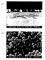
図7(a)および(b)に、実施例5の膜断面及び表面の走査型電子顕微鏡(SEM)写真を示した。
【0176】
(試料9の特性)
図8に試料9の反射スペクトルをレファレンスのガラス基板の反射スペクトルと共に示した。この結果は、熱処理条件を制御することにより、最低反射率を示す波長を制御できることを示している。粒子変形の効果と推定される。また、熱処理により、基材への粒子の密着性も向上した。
【0177】
図9(a)、(b)および図10(a)、(b)に、試料9の熱処理前及び75℃で100秒処理した後のSEM写真を示した。
【0178】
(試料10〜12の特性)
図11に透過スペクトルを示した。実線は試料10、破線は試料11、点線は試料12を示す。
【0179】
(試料13および試料14の特性)
図12に透過スペクトルを示した。実線は試料13、破線は試料14を示す。
【0180】
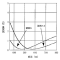
(二層品による最適反射防止波長の制御)
図13に反射スペクトルを示した。試料6は、MP-1040のみの一層品、試料13はスノーテックス50とMP-1040の二層品である。二層品にすることにより、最適反射防止波長を約480nmから約580nmにシフトさせることができた。
【0181】
(耐電防止性反射防止膜の分光特性)
図14に試料15の透過スペクトルを示した。図より明らかなように、可視光域において、透過率は95%を越え、最高97.8%であった。素TACの透過率は、素ガラスと同程度(92%弱)であった。なお、420nm以下の透過率ロスは、用いたTACフィルムの添加剤に基づく吸収によるものである。
【0182】
【発明の効果】
本発明の反射防止膜およびその製造方法によれば、高速で且つ大面積の部分に対して所望の透明基材上に微粒子層を容易に形成することができる。また、本発明においては、この微粒子層中の微粒子の付着量等を調整することが可能であり、反射防止効果を奏する最適な屈折率に設計することも可能である。したがって、低価格で高品質な反射防止膜を得ることができるという効果を奏する。
【図面の簡単な説明】
【図1】本発明の第2実施態様における付着手段の一例を説明する説明図である。
【図2】本発明の第3実施態様の製造方法における刷版作製工程の一例を示す説明図である。
【図3】実施例1および実施例2で得た試料の透過率を示すグラフである。
【図4】実施例3および実施例4で得た試料の反射率(入射角5°)を示すグラフである。
【図5】実施例5および実施例6で得た試料の透過率を示すグラフである。
【図6】実施例5および実施例6で得た試料の反射率(入射角5°)を示すグラフである。
【図7】(a)および(b)は実施例5で得た試料の平面および断面を示す走査型電子顕微鏡写真である。
【図8】実施例7で得た試料の反射率(入射角5°)を示すグラフである。
【図9】(a)および(b)は実施例7で得た加熱処理前の試料の平面および断面を示す走査型電子顕微鏡写真である。
【図10】(a)および(b)は実施例7で得た加熱処理後の試料の平面および断面を示す走査型電子顕微鏡写真である。
【図11】実施例8〜実施例10で得た試料の透過率を示すグラフである。
【図12】実施例11および実施例12で得た試料の透過率を示すグラフである。
【図13】実施例5および実施例11で得た試料の反射率を示すグラフである。
【図14】実施例13で得た試料の透過率を示すグラフである。
【符号の簡単な説明】
1 …… 基材
2 …… 高分子電解質膜
3 …… 微粒子層
4 …… 透明基材
5 …… 粘着層
8 …… 刷版[0001]
BACKGROUND OF THE INVENTION
The present invention relates to a display for personal use and commercial use such as CRT (cathode ray tube), LCD (liquid crystal display), plasma display, electroluminescence, television, personal computer, word processor, mobile phone, personal digital assistant, solar cell, The present invention relates to an antireflection film that can be used for lenses, window glass for buildings, window glass for vehicles, curved mirrors, rearview mirrors, goggles, and the like, and can improve visibility, efficiency, and the like, and a method for manufacturing the same.
[0002]
[Prior art]
As a conventional method for producing an antireflection film, a method of laminating an arbitrary number of layers on a substrate by controlling the thicknesses of a low refractive index layer and a high refractive index layer is widely used. However, this method has a problem that a vacuum apparatus is generally required and it is not a cost-effective manufacturing method. For this reason, various manufacturing methods that do not require a vacuum apparatus and structures that can reduce the number of layers have been proposed.
[0003]
Among these, in order to dramatically improve the antireflection characteristics, as a method of making the low refractive index layer an ultra-low refractive index layer into which pores / voids are introduced, for example, a fine particle layer is formed on a substrate by a coating method. A method of providing a single layer in a state having voids between the particles. According to such a method, low reflectivity due to a continuous change in the refractive index due to the surface shape effect of the fine particles, and also a bulk (with a thickness defined by the particle size) using voids between the particles (the refractive index of the voids is 1). Due to the low reflectivity due to the lowering of the refractive index of the layer), the antireflection film having high performance can be obtained by a simple production method.
[0004]
Examples of such a method include, for example, a coating film in which fine particles are closely packed and a method for producing the same (Japanese Patent Laid-Open No. 7-198904), and further dispersing and holding fine particles with a binder layer whose thickness is smaller than the particle size. Coating film (Japanese Patent Laid-Open No. 5-42211), coating film in which porous fine particles are formed on a single layer (Japanese Patent Laid-Open No. 5-13021), and binder portion of a film in which ultra fine particles are further dispersed and held by a binder For example, an antireflection film having a structure in which voids are removed by dry etching and voids are introduced between particles, and a manufacturing method thereof (Japanese Patent Laid-Open No. 7-104103).
[0005]
In addition, an antireflection film having a function similar to that of the above particle layer due to fine unevenness of the applied layer has been reported. For example, an antireflection film provided with fine irregularities by etching a layer composed of ultrafine particles and a binder, and a manufacturing method thereof (Patent No. 2858821), microphase separation of a polymer blend thin film, and specific components in the polymer There is an antireflection film (Ullrich Steiner et al., Science, 283, 520 pages, 1999) by a manufacturing method that forms fine voids / holes by solvent extraction.
[0006]
The various methods described above are all based on the concept of a simple process, but each has its own problems. That is, first, in various methods of providing a single particle layer, the step of providing a single particle layer on a substrate is performed by a coating method or a dip coating method as typified by a slide coating method. In a coating method represented by this slide coating method, the particles are not uniformly agglomerated as an irregular lump, and the region where the particles are not present is suppressed to an area that does not impair visibility and is uniformly applied. However, there was a problem that it was very difficult, and further, the coating speed could not be increased too much.
[0007]
On the other hand, the dip coating method has the same problem. Especially, the coating speed (base material pulling speed) is several tens of μmsec to obtain a uniform close-packed packing structure. -1 (Nagayama et al., Langmuir, Vol. 12, page 1303, 1999; Japanese Patent No. 2905712), which is extremely poor in industrial reality.
[0008]
[Problems to be solved by the present invention]
The present invention has been made in view of the above problems, and by positively using electrostatic interaction between the substrate surface and the particle surface in the particle suspension, emulsion or latex, An antireflection film having a fine particle layer formed without agglomerating fine particles into irregular lumps and without causing a region where the particles are not present to have such a size that visibility is not impaired, and A method for producing an antireflection film, which is capable of dramatically increasing the deposition rate of the fine particle layer as compared with the conventional method in principle, and thus provides a method for producing an antireflection film with good production efficiency. To do.
[0009]
[Means for Solving the Problems]
In order to achieve the above object, the present invention comprises a transparent base material and a fine particle layer having at least a single layer of fine particles arranged on the surface of the transparent base material, as described in
[0010]
As described above, in the present invention, the fine particles are arranged on the surface of the transparent substrate by electrostatic interaction between the surface of the transparent substrate and the fine particles to form a fine particle layer. Apply by a method such as immersing in a fine particle suspension, emulsion, or fine particle dispersion such as latex, and then wash away the particles that are not attached to the transparent substrate by electrostatic interaction. It is possible to form a fine particle layer, and the bulk (the whole fine particle layer formed by fine particles) using voids between fine particles in the fine particle layer (the refractive index is 1 when air exists in the voids) An antireflection film using low reflectivity due to a decrease in refractive index can be obtained, and an antireflection film having good performance can be obtained by a simple process.
[0011]
In the invention described in
[0012]
In order to adhere the transparent substrate surface and the fine particles by electrostatic interaction, it is necessary to impart a polarity different from the fine particles, that is, either positive or negative, to the transparent substrate surface. At this time, if either the positive or negative charge density on the surface of the transparent substrate is high, a fine particle layer in which fine particles are uniformly adhered can be formed on the transparent substrate, and a high-quality antireflection film can be obtained. In addition, since the polymer electrolyte can be arbitrarily selected from anionic property, cationic property, and their density and balance, the charge on the surface of the fine particles is not limited to either anion or cation. For these reasons, it is preferable to form a polymer electrolyte membrane made of a polymer electrolyte on the surface of the transparent substrate and use fine particles having a polarity different from that of the polymer electrolyte membrane.
[0013]
In this case, it is preferable that the polymer electrolyte membrane is a multilayer film formed by laminating two or more types of polymer electrolytes having different polarities. This is because unnecessary multi-layering of fine particles in the fine particle layer can be prevented, and a polymer electrolyte membrane having a uniform and high charge density can be obtained.
[0014]
In the invention described in
[0015]
In the antireflection film according to any one of
[0016]
Only electrostatic interaction may cause insufficient adhesion of fine particles to the surface of the transparent substrate, which may cause a problem in scratch resistance as an antireflection film. Therefore, in addition to electrostatic interaction, by attaching the fine particles to the surface of the transparent substrate by means of reinforcing adhesion, the anti-reflection film having good abrasion resistance and fine particles strongly adhere to the surface of the transparent substrate. can do.
[0017]
In the antireflection film according to
[0018]
The present invention further provides a bulk refraction having a transparent base material and at least a single layer of fine particles disposed on the surface of the transparent base material and having a refractive index lower than the refractive index of the transparent base material. A fine particle layer formed by adhering fine particles to the substrate surface by electrostatic interaction between the substrate surface and the fine particles on the other substrate surface. There is provided an antireflection film formed by transferring the fine particle layer onto the transparent substrate.
[0019]
Thus, if the fine particle layer in the antireflection film of the present invention is formed by electrostatic interaction on another substrate and transferred to a transparent substrate, positive or negative charge This is because it is possible to repeatedly use the base material having the above, which is advantageous in terms of cost.
[0020]
In this case, as described in claim 8, the adhesion due to electrostatic interaction between the other substrate surface and the fine particles is such that a polymer electrolyte membrane made of a polymer electrolyte is formed on the other substrate surface. It is preferable to use fine particles that are formed and have a polarity different from that of the polymer electrolyte membrane.
[0021]
For the same reason as in the case of
[0022]
In this case, as described in claim 9, the polymer electrolyte membrane is preferably a multilayer membrane formed by laminating two or more types of polymer electrolytes having different polarities. This is because unnecessary multi-layering of fine particles in the fine particle layer formed on the substrate can be prevented, and a polymer electrolyte membrane having a uniform and high charge density can be obtained.
[0023]
In the invention described in claim 8 or 9, as described in
[0024]
In the antireflection film according to any one of claims 7 to 10, as described in claim 11, adhesion between the fine particles in the fine particle layer and the surface of the transparent base material is prevented. Means for chemically and irreversibly bonding the transparent substrate surface and the fine particles, means for fusing the transparent substrate surface and the fine particles, means for forming a polymer thin film on the fine particle layer surface, and It is preferably made by at least one attachment means selected from the group consisting of means for forming an adhesive layer on the surface of the transparent substrate and causing the fine particles to adhere to the adhesive layer. This is because the adhesion force of the fine particles onto the transparent substrate can be increased, and the scratch resistance of the antireflection film can be improved.
[0025]
In the antireflection film according to any one of
[0026]
Further, in the antireflection film according to any one of
[0027]
On the other hand, in the antireflection film according to any one of
[0028]
Furthermore, in the antireflection film according to any one of
[0029]
Moreover, in the antireflection film according to any one of
[0030]
In the present invention, as described in claim 17, a charge imparting step for imparting a charge to the surface of the transparent substrate and fine particles having a surface charge with a sign opposite to the charge imparted to the surface of the transparent substrate are contained. An antireflection film comprising: a fine particle layer forming step of applying a fine particle dispersion onto the transparent substrate to form a fine particle layer; and a cleaning step of cleaning the transparent substrate on which the fine particle layer is formed. A manufacturing method is provided.
[0031]
As described above, since the formation of the fine particle layer on the transparent substrate can be performed by applying the fine particle dispersion containing fine particles and then washing, the manufacturing process is simple and efficient. . Therefore, it is possible to manufacture the antireflection film with an advantage in cost.
[0032]
At this time, as described in claim 18, the charge imparting step for imparting electric charge to the surface of the transparent substrate is formed by laminating at least two kinds of polymer electrolytes having different polarities on the surface of the transparent substrate. The step of providing a polymer electrolyte membrane made of a multilayer film and / or a polymer electrolyte membrane made of a crosslinked polymer electrolyte is preferred for the reasons described in the explanations of
[0033]
Further, according to the present invention, as described in claim 19, a charge imparting step for imparting a charge to the surface of the substrate, and a fine particle dispersion containing fine particles having a surface charge opposite in sign to the charge imparted to the substrate surface The liquid is applied onto the transparent substrate to form a fine particle layer, the washing step to wash the substrate on which the fine particle layer is formed, and the fine particle layer formed on the substrate is transparent. There is provided a method for producing an antireflection film, comprising a transfer step of transferring onto a substrate.
[0034]
As described above, once the fine particle layer is formed on the base material and the antireflection film is formed by transferring the fine particle layer onto the transparent base material, a charge applying step for applying a charge only to the surface of the base material is performed. By applying and repeatedly using this base material, it is not necessary to perform a charge imparting step on the transparent base material. Therefore, for example, it is not necessary to perform a charge imparting process such as formation of a polymer electrolyte film for each transparent substrate, so that the process can be simplified and an antireflection film is formed with an advantage in cost. be able to.
[0035]
In this case, as described in claim 20, in the transfer step, the adhesion means between the fine particles in the fine particle layer and the surface of the transparent substrate causes the transparent substrate surface and the fine particles to be chemically and irreversibly. Means for bonding to the transparent substrate surface and the fine particles, means for forming a polymer thin film on the fine particle layer surface, and forming an adhesive layer on the transparent substrate surface to adhere the fine particles to the fine particles. It is preferably at least one means selected from the group consisting of means for adhering onto the layer. This is for improving the scratch resistance of the antireflection film finally obtained.
[0036]
Furthermore, the present invention provides, as described in claim 21, a fine particle containing a charge imparting step for imparting a charge to the surface of the substrate, and a fine particle having a surface charge with a sign opposite to the charge imparted to the surface of the substrate. A dispersion layer is applied on the transparent base material to form a fine particle layer, a fine particle layer forming step, a cleaning step of cleaning the base material on which the fine particle layer is formed, and the transparent base material cleaned in the cleaning step Using the upper fine particle layer as an original plate, a plate making process is performed by using a printing plate material to form a printing plate, and a fine particle replication layer is formed on a transparent substrate using the printing plate produced in the above plate making process. There is provided a method for producing an antireflection film, comprising a fine particle replication layer forming step. By making a printing plate in this way and using it to duplicate the antireflection film, the conventional lens film and light diffusion film manufacturing process can be used as it is, so the initial investment can be reduced, and the result This is because the cost of the antireflective film obtained can be reduced.
[0037]
In the invention according to any one of claims 19 to 21, as described in claim 22, a charge imparting step for imparting a charge to the substrate surface is performed on the substrate surface. The above-mentioned process is a step of providing a polymer electrolyte membrane comprising a multilayer film formed by laminating at least two types of polymer electrolytes having different polarities and / or a polymer electrolyte membrane comprising a crosslinked polymer electrolyte. It is preferable for the reasons described in the description of items 8 to 10.
[0038]
DETAILED DESCRIPTION OF THE INVENTION
The present inventor is a known phenomenon that a fine particle is adsorbed, adhered or adhered to the surface of the substrate due to electrostatic interaction between the charge on the surface of the substrate and the charge on the surface of the fine particles in the diluted fine particle suspension. In order to complete the present invention, the present invention can be applied to a method for producing an antireflection film, and further, by examining various film formation conditions of a fine particle film in which fine particles adhere to the surface of the substrate, various film formation conditions can be found. It has come. Hereinafter, such an antireflection film of the present invention will be described in detail.
[0039]
The antireflection film of the present invention includes a first embodiment formed by providing a fine particle layer directly on a transparent substrate, and the fine particle layer is once formed on another substrate. It can be divided into a second embodiment formed by transferring it onto.
Each embodiment will be described below.
[0040]
1. First embodiment
The antireflection film according to the first embodiment of the present invention has a transparent base material and a fine particle layer having at least a single layer of fine particles disposed on the surface of the transparent base material. Is adhered by at least electrostatic interaction, and the bulk refractive index of the fine particle layer is lower than the refractive index of the transparent substrate.
[0041]
Such a feature of the present embodiment resides in that fine particles are arranged on the transparent substrate surface by electrostatic interaction between the transparent substrate surface and the fine particles to form a fine particle layer. Since this embodiment has such a feature, a transparent substrate is simply subjected to various dispersion methods such as those described later, and a fine particle dispersion such as a relatively concentrated fine particle suspension, emulsion, or latex. It is possible to uniformly form a fine particle layer simply by applying and then washing away the particles that are not adhered to the transparent substrate by electrostatic interaction. Therefore, it is possible to uniformly apply fine particles onto a transparent substrate, which has been difficult with the conventionally proposed methods for producing an antireflection film, so that an antireflection film with higher quality can be obtained. Furthermore, in this embodiment, the above-mentioned fine particle dispersion can be applied onto the transparent substrate in a short time by using, for example, a dip coating method. Therefore, it can be manufactured in a short time compared to the conventional method of manufacturing an antireflection film using fine particles, and thus the cost of the finally obtained antireflection film can be reduced. Furthermore, in this embodiment, for example, by using a dip coating method, an antireflection film is formed not only on a flat surface but also on a curved surface, the inner surface of a cylindrical structure, a complicated shape surface, or the like. Can do.
[0042]
Hereinafter, the antireflection film of the first embodiment will be described separately for each configuration.
[0043]
(Transparent substrate)
The transparent base material used in this embodiment can be any transparent base material that is transparent in the visible light region that is normally used for an antireflection film. As specific materials, resin, glass, metal, ceramics, etc. can be applied, and in terms of shape, in addition to films, sheets, plates, etc., as described above, curved shapes, cylindrical structures, complex shapes, etc. Any shape of transparent substrate can be used.
[0044]
Examples of resin base materials include triacetyl cellulose, diacetyl cellulose, acetate butyrate cellulose, polyether sulfone, polyacrylic resin, polyurethane resin, polyester, polycarbonate, polysulfone, polyether, trimethylpentene, polyether ketone, (meta ) Acrylonitrile and the like.
[0045]
As the transparent substrate used in the present embodiment, those using PET, glass or the like as a material are common.
[0046]
(Fine particles)
The fine particles used in the present embodiment are fine particles that are transparent in the visible light region, and fine particles that can have a refractive index smaller than the refractive index of the transparent substrate as a bulk refractive index when a fine particle layer described later is formed. If it is, it will not specifically limit.
[0047]
Specifically, inorganic fine particles that can be used include MgF. 2 (Refractive index 1.38), SiO 2 (Refractive index 1.46), AlF Three (Refractive index 1.33-1.39), CaF 2 (Refractive index 1.44), LiF (refractive index 1.36 to 1.37), NaF (refractive index 1.32 to 1.34), ThF Four Fine particles such as (refractive index 1.45 to 1.5).
[0048]
Examples of the fine particles of the organic material include fine particles of polymers. Specifically, crosslinked acrylic fine particles (for example, MX series and MR series manufactured by Soken Chemical Co., Ltd.), non-crosslinked acrylic fine particles (for example, , MP series manufactured by Soken Chemical Co., Ltd.), cross-linked polystyrene fine particles (for example, SGP series manufactured by Soken Chemical Co., Ltd.), non-cross-linked polystyrene fine particles, monodisperse polymethyl methacrylate fine particles with high cross-linking degree (for example, Soken Chemical ( MS series, M series), composite fine particles, and functional group-introduced fine particles.
[0049]
In this embodiment, silica (SiO 2 It is preferable to use fine particles or fine particles of polymers.
[0050]
The average particle size of the fine particles that can be used in this embodiment is preferably from 50 nm to 300 nm, and more preferably from 70 nm to 250 nm. When the average particle size is smaller than the above range, when the fine particles are formed as a single layer to form a fine particle layer, the film thickness of the fine particle layer may be too thin to obtain a sufficient antireflection effect. It is not preferable. Further, when the average particle diameter exceeds the above range, when the fine particles are formed into a single layer, the visible light incident on the fine particle layer is scattered and diffusely reflected, which is not preferable because the visible light transmittance is lowered. . This phenomenon is particularly remarkable when observed from an oblique direction. That is, when it is formed with fine particles exceeding the above range, it becomes an antireflection film having low transmittance and high angle dependency, and generally has a high possibility of being defective as an antireflection film.
[0051]
The particle size distribution of the fine particles used is not particularly limited, but those having a relatively small particle size distribution are preferred. Specifically, it is preferable not to include fine particles having a particle size exceeding 300 nm, that is, the particle size distribution range is 300 nm or less.
[0052]
Further, the refractive index of the fine particles is particularly limited as long as the refractive index of the fine particle layer can be formed so that the refractive index of the fine particle layer is smaller than the refractive index of the transparent substrate when the fine particle layer described later is formed. However, those having a small refractive index are preferably used. A desirable refractive index of the fine particles is desirably in the range of 1.05 to 1.70, particularly in the range of 1.05 to 1.55.
[0053]
In the present invention, conductive fine particles can also be used as the fine particles because an antistatic effect can be imparted in addition to the antireflection effect. These conductive fine particles may be used alone, or SiO 2 You may make it use together with microparticles | fine-particles with low refractive index, such as.
[0054]
Such conductive fine particles are not particularly limited as long as they are fine particles having a certain degree of conductivity. For example, tin oxide (SnO 2 ), Antimony-doped tin oxide, phosphorus-doped tin oxide, zinc oxide (ZnO), indium oxide (In 2 O Three ), Tin-doped indium oxide, and the like.
[0055]
In the case of using such conductive fine particles, the average particle size of the fine particles is preferably 1 nm or more and less than 50 nm, particularly 1 nm or more and less than 35 nm, particularly 1 nm or more and less than 30 nm from the viewpoint of antistatic properties. preferable. In addition, when the conductive fine particles are acicular particles, they can be suitably used as long as the minor axis length satisfies the above average particle diameter condition.
[0056]
(Fine particle layer)
Such fine particles are deposited on the transparent substrate to form a fine particle layer. The fine particles in the fine particle layer may be attached as a single layer or may be formed as a plurality of layers. In the case of being formed of a plurality of layers, a plurality of types of fine particles, for example, fine particles having different refractive indexes may be used for each layer.
[0057]
In the present embodiment, the fine particle layer may be formed only on one side of the base material, or may be formed on both sides when the base material is a plate-like substrate.
[0058]
In the fine particle layer in the present embodiment, a preferable adhesion amount of the fine particles on the transparent substrate, in other words, as a preferable filling amount of the fine particles in the fine particle layer, this adhesion amount is a volume percentage of the fine particles in the fine particle layer, That is, when the fine particle occupancy per unit volume of the fine particle layer is set, it is preferably in the range of 10% by volume to 90% by volume, and particularly preferably in the range of 20% by volume to 80% by volume. When the volume fraction of the fine particles is smaller than the above range, the fine particle layer may not be optically recognized as a layer, which is not preferable in that the antireflection effect may not be achieved. On the other hand, when the volume fraction is larger than the above range, the gap between the fine particles decreases, and the gap between the fine particles reduces the bulk refractive index of the fine particle layer and improves the antireflection effect. This is not preferable because it may not be possible to achieve a satisfactory effect. The upper limit of the volume percentage of fine particles in the fine particle layer when the fine particles are spherical and monodispersed is 60% by volume when the fine particles in the fine particle layer is a single layer, regardless of the above range. Is 74% by volume.
[0059]
In the present embodiment, the volume fraction of the fine particles in the fine particle layer, that is, the fine particle occupation rate per unit volume of the fine particle layer is obtained by the following two methods.
[0060]
The first method is a method of calculating using the following equation (a) when the volume fraction is Φ.
[0061]
Φ = πa Three N / 6Sd, where d ≧ an (a)
Here, S is the substrate surface area, a is the average particle size of the fine particles, d is the total particle layer thickness, n is the number of particle layers, and N is the number of particles. These values are obtained by actual measurement from the fine particle layer surface and cross-sectional photographs.
[0062]
In particular, in the case of a single particle layer, d = a can be considered and the following formula (b) can be used.
[0063]
Φ = πa 2 N / 6S (b)
[0064]
The second method is a method of calculating using the following equation (c).
Φ = (n cal -N air ) / (N p -N air (C)
Where n p Indicates the refractive index of the particle, n air Indicates the refractive index of the gap between particles, n cal Indicates the bulk refractive index of the fine particle layer determined by simulation. In addition, since the fine particle layer of the present invention is sufficiently transparent, the bulk refractive index of the fine particle layer is obtained by simulation using data such as a reflection spectrum regardless of whether the fine particle layer is a single layer or a multilayer. Can do.
[0065]
The fine particle layer in this embodiment is usually formed by the fine particles and a gas (usually air) existing therebetween. However, in the present embodiment, the present invention is not limited to this. For example, in the case where a reinforcing attachment means described later is used, a predetermined resin or the like may be present instead of the gas.
[0066]
In the present embodiment, the refractive index of the fine particle layer as a bulk including such fine particles and the gas existing therebetween and also the resin existing as other components needs to be smaller than the refractive index of the transparent substrate. There is. This is because when the bulk refractive index is the same as or larger than the refractive index of the transparent substrate, the antireflection effect cannot be imparted.
[0067]
The bulk refractive index in the fine particle layer is an important factor that greatly affects the antireflection effect. In this embodiment, the bulk refractive index of the fine particle layer can be adjusted relatively easily. That is, by adjusting the kind of fine particles to be attached, the amount to be attached, etc., it is possible to easily set the refractive index of the bulk to the optimum value, thereby obtaining an antireflection film having the best antireflection effect. Can do. The optimum value of the refractive index of the bulk varies depending on the type of the transparent substrate, but when the transparent substrate is general-purpose glass, PET, or the like, it is usually in the range of 1.05 to 1.60. In particular, it is desirable that it is in the range of 1.05 to 1.50, particularly in the range of 1.05 to 1.46.
[0068]
Further, the film thickness of the fine particle layer also greatly affects the antireflection effect, but in the present embodiment, it is preferably in the range of 50 nm to 300 nm, and particularly in the range of 70 nm to 250 nm. preferable. This is because if the film thickness of the fine particle layer is out of the above range, the antireflection effect of the finally obtained antireflection film is reduced.
[0069]
In the present invention, as described above, a plurality of fine particle layers may be provided. At this time, one layer is a thick layer using fine particles having a relatively large particle size, and the other layers are compared. It is preferable to have a two-layer structure with a thin layer using fine particles having a small target particle size. This is due to the following reason.
[0070]
Generally, by changing the film thickness of the fine particle layer, that is, the particle diameter of the fine particles in the fine particle layer, the wavelength at which the film prevents reflection most can be changed. Specifically, as the film thickness of the fine particle layer (particle diameter of the fine particles) increases, the wavelength of the light that prevents the reflection most increases. Therefore, the particle size of the fine particles may be selected and used according to the application of antireflection, and the fine particle layer may be formed so that the antireflection effect is the best. However, the particle size of commercially available fine particles is often limited to a certain particle size, and there are cases where fine particles having a required particle size are not available.
[0071]
In such a case, a fine particle layer is formed using the above-mentioned commercially available fine particles having a certain particle size (fine particle layer using fine particles having a large particle size), and a fine particle layer using fine particles having a smaller particle size. By forming, the wavelength having the highest antireflection effect can be moved and adjusted to the position where the antireflection effect is most efficient.
[0072]
In this case, in the fine particle layer using fine particles having a large particle diameter, the film thickness of the fine particle layer is preferably in the range of 50 to 300 nm, and particularly preferably in the range of 70 to 180 nm. In this case, it is preferable to use fine particles having an average particle diameter in the range of 50 to 300 nm, and it is particularly preferable to use fine particles having an average particle diameter in the range of 70 to 180 nm. This is because, as described above, when the average particle size is smaller than the above range, it is not preferable because the film thickness of the fine particle layer may be too thin to obtain a sufficient antireflection effect. If the average particle size exceeds the above range, the visible light incident on the fine particle layer is scattered and diffusely reflected, which is not preferable because the visible light transmittance is lowered.
[0073]
On the other hand, in the fine particle layer using fine particles having a small particle diameter, the film thickness of the fine particle layer is in the range of 1 to 50 nm, and particularly preferably in the range of 1 to 30 nm. In this case, it is preferable to use fine particles having an average particle diameter of 1 to 50 nm, and it is particularly preferable to use fine particles having an average particle diameter of 1 to 30 nm. The smaller the average particle size of the fine particles, the more preferable is that the position of the wavelength having the highest antireflection effect can be finely adjusted. However, if the average particle size is smaller than the above range, a problem may occur in the handling of the fine particles. Because there is sex.
[0074]
In the present invention, the layer using fine particles having a large particle size is not limited to a single layer, and may be composed of a plurality of layers. Similarly, the layer using fine particles having a small particle diameter is not necessarily a single layer, and may be a plurality of layers. Any of the layer using fine particles having a large particle diameter and the layer using fine particles having a small particle diameter may be formed on the transparent substrate first.
[0075]
In the present invention, the material of the fine particles used for the layer having a large particle diameter and the material of the fine particles used for the layer having a small particle diameter may be the same material or different materials. Good. For example, as a material of large particles, SiO 2 A material having a relatively small refractive index such as the above may be selected, and the conductive fine particles such as tin oxide described above may be used as the material for the particles having a small particle diameter. Accordingly, it is possible to adjust the position of the wavelength having the highest antireflection effect to improve the antireflection effect as a whole and to impart an antistatic effect to the antireflection film.
[0076]
(Electrostatic interaction)
One of the features of this embodiment is that fine particles are adhered to the transparent substrate by at least electrostatic interaction. As described above, the adhesion of the fine particles on the transparent substrate, in other words, the formation of the fine particle layer on the transparent substrate is performed by electrostatic interaction. Therefore, in this embodiment, the fine particles are uniformly transparent. A fine particle layer which is disposed on the material and has a high antireflection effect can be formed on the transparent substrate.
[0077]
In the case of attaching fine particles on a transparent substrate by such electrostatic interaction, there is no particular limitation, but usually a positive or negative charge is imparted on the transparent substrate, and the opposite of this charge is applied. By using polar fine particles, a method of adhering the fine particles on the transparent substrate by electrostatic interaction is employed.
[0078]
As a method for imparting a charge to the transparent substrate surface, there are a case where the surface of the transparent substrate is simply charged and a case where an ionic functional group is imparted to the surface of the transparent substrate physically or chemically. In the present embodiment, since the former has poor charge stability, it is preferable to use the latter method of imparting an ionic functional group to the substrate surface.
[0079]
Examples of techniques for introducing ionic functional groups on the surface of the substrate include corona discharge treatment, glow discharge treatment, plasma treatment, hydrolysis treatment, silane coupling treatment, polymer electrolyte coating, and formation of a polymer electrolyte multilayer film. In this embodiment, it is preferable to form a polymer electrolyte membrane obtained by applying a polymer electrolyte or the like. This is due to the following reason.
[0080]
First, in general, when the charge density on the surface of the transparent substrate is higher, a fine particle layer having a higher antireflection effect in which fine particles are uniformly adhered on the transparent substrate can be formed. On the other hand, by forming the polymer electrolyte membrane on the transparent substrate, the charge density can be increased as compared with other methods. Therefore, the polymer electrolyte membrane is formed on the transparent substrate, and the fine particles are deposited on the transparent substrate, that is, on the polymer electrolyte by electrostatic interaction between the polymer electrolyte membrane and the fine particles. It can be a fine particle layer that adheres uniformly, and can be an antireflection film having a high antireflection effect.
[0081]
In corona discharge treatment, glow discharge treatment, plasma treatment, and hydrolysis treatment, generally introduced ionic functional groups are often anionic groups. Therefore, the charge on the surface of the fine particles is limited to cations. On the other hand, since the polymer electrolyte can be arbitrarily selected from anionicity, cationicity, and their density and balance, the charge on the surface of the fine particles is not limited to either anion or cation. Also from this point, it is preferable to form a polymer electrolyte membrane made of a polymer electrolyte as a method for imparting a charge to the transparent substrate surface.
[0082]
In addition, since the transparent base material surface is often hydrophobic, it is effective to use the above method in combination as a method for imparting a sufficient charge to the base material surface. For example, after applying at least one of corona discharge treatment, glow discharge treatment, plasma treatment, hydrolysis treatment, silane coupling treatment to the surface of the base material, polymer electrolyte coating or polymer electrolyte multilayer film formation is performed. Is also possible and is the preferred method.
[0083]
When a polymer electrolyte membrane is formed to impart a charge to the surface of the transparent substrate, the thickness of the polymer electrolyte membrane is preferably thinner than the average particle size of the fine particles, and the thickness of the polymer electrolyte is further reduced to the average particle size of the fine particles It is preferable to be less than 50% of the diameter. When the film thickness of the polymer electrolyte membrane is equal to or greater than the average particle size of the fine particles, the fine particles are partially laminated in two or more layers to scatter incident visible light, reduce or fill voids between the fine particles, The antireflection film is not preferable because it may be a defective film.
[0084]
In the present embodiment, such a polymer electrolyte membrane is preferably a multilayer film formed by laminating two or more types of polymer electrolytes having different polarities. As a method for forming such a polymer electrolyte multilayer film, a known so-called alternating adsorption film manufacturing method (Layer-by-Layer Assembly method) can be suitably used. This method is a method of forming a polymer electrolyte multilayer film on a substrate with nano-order film thickness control by alternately immersing the substrate in a cationic polymer electrolyte aqueous solution and an anionic polymer electrolyte aqueous solution. (Eg Gero Decher et al., Science, 277, 1232, 1997; Shiratori Semei et al., IEICE Tech., OME98-106, 1998; Joseph B. Schlenoff et al., Macromolecules, 32, 8153, 1999. Year). According to this method, even if the polymer electrolyte multilayer film is thicker than the particle diameter of the fine particles, the fine particle film is formed as a single particle film. This is because the polymer electrolyte multilayer film is a polymer complex that is insoluble in the medium (mainly water), hardly diffuses into the medium, and the microparticles interact almost only with the surface of the polymer electrolyte multilayer film. is there.
[0085]
There have already been many reports of examples of producing alternating multilayer films using polymer electrolytes and fine particles, or producing single particle films (for example, alternating multilayer films: Kunitake et al., Chemistry Letters, page 125, 1997). Single particle film: Akashi et al., Langmuir, 14, 4088, 1998). However, in the prior art including these, there is no report / description focusing on the antireflection function of the single particle film.
[0086]
In this embodiment, the polymer electrolyte forming the polymer electrolyte membrane is preferably a crosslinked polymer electrolyte. This is because the use of a crosslinked polymer electrolyte can prevent unnecessary and inconvenient multilayering of particles in the fine particle layer. This cross-linked polymer electrolyte is preferably used when the polymer electrolyte is formed as a single layer or when the polymer electrolyte multilayer film is used. When the polymer electrolyte multilayer film is used, only the uppermost layer is used. A cross-linked polymer electrolyte may be used, or all layers may be formed of a cross-linked polymer electrolyte.
[0087]
In the present embodiment, when a fine particle layer is formed by electrostatic interaction using such a polymer electrolyte membrane, and when a plurality of fine particles are formed, a polymer electrolyte membrane is formed and fine particles are formed thereon. After the step of depositing the polymer electrolyte membrane, the method of repeating the step of forming the polymer electrolyte membrane thereon and depositing the fine particles again, or forming the polymer electrolyte with a predetermined film thickness and bringing it into contact with the fine particle dispersion For example, a method of forming a plurality of fine particles by swelling the polymer electrolyte membrane and incorporating the fine particles into the polymer electrolyte membrane can be used.
[0088]
Examples of the polymer electrolyte used in this embodiment include polyethyleneimine and its quaternized product, polydiallyldimethylammonium chloride, poly (N, N′-dimethyl-3,5-dimethylene-piperidinium chloride), polyallylamine and Quaternized product thereof, polydimethylaminoethyl (meth) acrylate and quaternized product thereof, polydimethylaminopropyl (meth) acrylamide and quaternized product thereof, polydimethyl (meth) acrylamide and quaternized product thereof, poly (meth) acrylic Acid and its ionized product, polystyrene sodium sulfonate, poly (2-acrylamido-2-methyl-1-propanesulfonic acid), polyamic acid, potassium polyvinyl sulfonate, and monomers constituting the polymer and (meth) acrylic acid A copolymer with a nonionic aqueous monomer such as imide, 2-hydroxyethyl (meth) acrylate, N-isopropyl (meth) acrylamide can be raised.
[0089]
In this embodiment, among others, polyethyleneimine quaternized product, polydiallyldimethylammonium chloride, poly (N, N'-dimethyl-3,5-dimethylene-piperidinium chloride), polyallylamine quaternized product, polydimethylaminoethyl (Meth) acrylate quaternized product, polydimethylaminopropyl (meth) acrylamide quaternized product, polydimethyl (meth) acrylamide quaternized product, sodium poly (meth) acrylate, sodium polystyrene sulfonate, poly (2-acrylamide-2) -Methyl-1-propanesulfonic acid), potassium polyvinyl sulfonate, and monomers constituting the polymer and (meth) acrylamide, 2-hydroxyethyl (meth) acrylate, N-isopropyl (meth) acrylamide, etc. It is preferable to use a copolymer with a nonionic aqueous monomer.
[0090]
The crosslinked polymer electrolyte includes a crosslinked product of a monomer constituting the polymer electrolyte and a polyfunctional monomer such as methylenebisacrylamide, a crosslinked product obtained by reaction of the polymer electrolyte with aldehydes, and the polymer. Examples thereof include a cross-linked product obtained by electron beam and gamma ray irradiation on the electrolyte.
[0091]
(Reinforcing attachment means)
The antireflection film of this embodiment is formed by forming fine particle layers by attaching fine particles to a transparent base material by electrostatic interaction. The fine base material is transparent substrate only by electrostatic interaction. If it adheres to the surface, there may be a problem in scratch resistance or the like in actual use. In such a case, a reinforcing attachment means for improving the adhesion force of the fine particles onto the transparent substrate may be used.
[0092]
Such reinforcing adhesion means is not limited to this, but means for chemically and irreversibly bonding the surface of the transparent base material and the fine particles, means for fusing the surface of the transparent base material and the fine particles. And a means for forming a polymer thin film on the surface of the fine particle layer. These can be used alone or in combination.
[0093]
The means for chemically and irreversibly bonding the transparent substrate surface and the fine particles is a means for forming a general ester bond, urethane bond, amide bond, ether bond, etc. between the transparent substrate surface and the fine particles. It is. That is, by introducing a functional group capable of forming a chemical and irreversible bond as described above by bonding to the surface of the transparent substrate and the surface of the fine particle, respectively, during or after the formation of the fine particle layer by electrostatic interaction In the process, this functional group is reacted to form a chemical and irreversible bond as described above. The type of chemical bond to be used or the type of functional group to be introduced can be appropriately selected in consideration of the transparent substrate, the type of fine particles, the reactivity, and the like.
[0094]
The means for fusing the transparent substrate surface and the fine particles is to form a fine particle layer by electrostatic interaction, and then heat the fine particles and / or the transparent substrate to fuse the transparent substrate surface and the fine particles. It is a means to make. When this means is used, when an inorganic oxide such as silica or a metal oxide is used as the fine particles, the transparent substrate is preferably inorganic glass. This is because if the transparent substrate is a polymer, the transparent substrate cannot withstand the temperature at which the fine particles are fused. On the other hand, when the fine particles are a polymer, it goes without saying that the polymer can be used for the transparent substrate. In this case, the glass transition temperature of the transparent substrate is preferably higher than the glass transition temperature of the fine particles, and more preferably, the glass transition temperature of the transparent substrate is higher than the minimum film-forming temperature of the fine particles.
[0095]
In the case of using this means, the polymer fine particles (polymer fine particles) may be crosslinked to the extent that they can be fused to the transparent substrate. The polymer fine particles may be so-called core-shell particles having a core having a high glass transition temperature and a shell having a low glass transition temperature. In this case, the glass transition temperature of the core may be higher than the glass transition temperature of the substrate.
[0096]
Further, when this means is used, two or more kinds of fine particles may be used in combination. For example, by forming a single particle film on a polymer transparent substrate using silica particles and polymer particles together, and then fusing the polymer particles to the substrate and silica particles appropriately, adhesion and scratch resistance It is possible to obtain an antireflection film excellent in both properties.
[0097]
The means for forming a polymer thin film on the surface of the fine particle layer is to form fine particle layers on the transparent substrate by depositing fine particles by electrostatic interaction and forming a fine particle layer on the fine particle layer. Means. Also by such a method, the anti-scratch property of the antireflection film can be enhanced, and further, the antifouling property can be enhanced by using a fluororesin for the polymer thin film. In the case where the means for forming the polymer thin film on the surface of the fine particle layer is used as described above, the refractive index as a bulk of the fine particle layer containing the polymer thin film can be made smaller than that of the transparent substrate as described above. is necessary.
[0098]
In this case, in order to obtain higher scratch resistance, it is possible to use a crosslinked polymer thin film. In this case, the case where the functional group on the surface of the fine particle reacts with the functional group contained in the polymer forming the polymer thin film is also included in the crosslinking.
[0099]
(Other)
In the antireflection film of this embodiment, other layers such as a high refractive index layer, a medium refractive index layer, a hard coat, etc. are formed between the transparent base material and the fine particle layer in the same manner as a normal antireflection film. Also good.
[0100]
2. Manufacturing method of the first embodiment
The antireflection film of the first embodiment includes a charge imparting step for imparting a charge to the surface of the transparent substrate, and a fine particle dispersion containing fine particles having a surface charge opposite in sign to the charge imparted to the surface of the transparent substrate. Can be produced by applying a fine particle layer on the transparent substrate to form a fine particle layer, and a washing step for washing the transparent substrate on which the fine particle layer is formed. Hereinafter, the manufacturing method of this 1st embodiment is demonstrated.
[0101]
(Charge application process)
In the manufacturing method of this embodiment, first, a charge imparting step for imparting a charge to the transparent substrate surface is performed. The charge imparting method for the transparent substrate is to impart charges to the transparent substrate by the same method as described in the section of (electrostatic interaction) in the description of the first embodiment. Therefore, the detailed description here is omitted, but the most preferable method (process) is formed by laminating at least two kinds of polymer electrolytes having different polarities on the surface of the transparent substrate, as described above. A step of providing the multilayer film.
[0102]
(Particle layer formation process)
The fine particle dispersion is applied on the transparent substrate thus charged to form a fine particle layer. The coating method at this time is not particularly limited, and various known coating methods such as spray coating and bar coating can be used. However, a transparent substrate in which a charge is added to the fine particle dispersion. A method of immersing the material is particularly preferably used.
[0103]
The fine particle dispersion used in this step is formed by dispersing and suspending fine particles in a suitable medium. As the medium system, an aqueous system is most preferable. This is because this embodiment uses the electrostatic interaction between the transparent substrate surface and the fine particle surface. Further, an emulsifier or a dispersion stabilizer may be used in order to stably disperse and suspend the fine particles. In this case, it is preferable that the emulsifier and the dispersion stabilizer are ionic, and it is preferable that the emulsifier and the dispersion stabilizer have the opposite sign to the charge on the surface of the substrate, that is, the ionic sign having the same sign as the surface charge of the fine particles.
[0104]
A commercially available product can be used as the fine particle dispersion having such a composition. Specific examples include various colloidal silicas manufactured by Nissan Chemical Industries, various acrylic emulsions and various latexes manufactured by JSR. In addition, fine particles such as various fine polymer powders manufactured by Soken Chemical Co., Ltd. can be obtained as powders and dispersed in water in the presence of a suitable emulsifier or dispersion stabilizer to form a fine particle dispersion.
[0105]
The pH of commercially available fine particle dispersions as described above varies from acidic to alkaline. In the charge imparting step, the surface of the polymer electrolyte membrane on the transparent substrate or the multilayer film formed by laminating the polymer electrolyte is formed of a weak electrolyte polymer, and this is a carboxylic acid-based polymer. In the case of a weak anionic polymer electrolyte such as a molecule, the pH of the fine particle dispersion is preferably neutral to alkaline. This is because weak anions such as carboxyl groups do not ionically dissociate under acidic conditions. For example, in the case of a weak cationic polymer electrolyte such as an imine polymer, the pH of the fine particle dispersion is preferably neutral to acidic. This is because a weak cation such as an imino group is not ionically dissociated under alkaline conditions. When a strong anionic polymer electrolyte such as polystyrene sulfonate sodium salt or a strong cationic polymer electrolyte such as polydiallyldimethylammonium chloride is used, a fine particle dispersion from acidic to alkaline can be used. This is because strong electrolytes are less susceptible to pH in ion dissociation properties.
[0106]
By adjusting the concentration of such a fine particle dispersion, it is possible to change the density of the fine particles in the formed fine particle layer. Since the refractive index of the bulk in the fine particle layer can be changed by changing the density of the fine particles in the fine particle layer, the concentration of the fine particles in the fine particle dispersion is determined by the reflection performance of the obtained antireflection film. It can be said that this is a factor that greatly affects The concentration of fine particles in such a fine particle dispersion greatly varies depending on various factors such as the target bulk particle refractive index, the kind of fine particles, and what kind of dispersion the dispersion is. However, in general, those in the range of 3 to 60% by weight, preferably 5 to 50% by weight are used.
[0107]
The fine particle layer forming step in the production method of the present embodiment is completely different from the method of forming a film at the time of pulling down the substrate or pulling up the substrate, such as the so-called Langmuir-Blodgett method or dip coating method. In a preferred embodiment of this step, the film is formed in a state where the transparent substrate is immersed in the fine particle dispersion. Therefore, in the case of single wafer type film formation, the film formation time is the same in principle regardless of the size of the substrate. In other words, the required immersion time of the substrate in the fine particle dispersion is the same regardless of the size of the substrate. On the other hand, in the case of the Langmuir-Blodgett method or the dip coating method, the optimum substrate pull-down speed or the optimum substrate pull-up speed is specified, so that the film formation time becomes longer as the substrate becomes larger. In addition, in this step, the immersion time can be set to several seconds. Further, this process has an advantage that it can be applied not only to a single wafer type but also to a so-called winding type.
[0108]
(Washing process)
After the fine particle layer forming step is performed in this manner, the cleaning step is performed, whereby the fine particles not attached to the transparent substrate are washed away by electrostatic interaction in the fine particle forming step. This cleaning step can be performed in the same manner as a general cleaning step.
[0109]
(Other)
In addition, if necessary, the step of adding the reinforcing attachment means may be performed in the same manner as described in the column of (Reinforcing attachment means) of the first embodiment. By performing such a process, the scratch resistance of the obtained antireflection film can be improved.
[0110]
3. Second embodiment
A second embodiment of the antireflection film of the present invention comprises a transparent base material, a bulk refractive index which is disposed on the surface of the transparent base material, has at least a single layer of fine particles, and is lower than the refractive index of the transparent base material. At least a fine particle layer having
The fine particle layer is a fine particle layer formed by adhering fine particles to the substrate surface by electrostatic interaction between the substrate surface and the fine particles on the other substrate surface, and the fine particle layer is formed on the transparent substrate. It is characterized by being formed by being transferred to the surface.
[0111]
This embodiment is different from the first embodiment in that this embodiment is such that a fine particle layer by electrostatic interaction is formed in advance on another substrate different from the transparent substrate of the antireflection film, It exists in the point formed by transcribe | transferring on a transparent base material. By adopting such a configuration, the second embodiment has the following advantages.
[0112]
That is, in this embodiment, it is possible to repeatedly use this other base material by applying a charge to the other base material in advance. Therefore, it is not necessary to always perform a charge application step in manufacturing each antireflection film, which is advantageous in terms of cost.
[0113]
In addition, the other base material forming the fine particle layer itself does not become a transparent base material of the final antireflection film, so that it is not necessary to be transparent, and there is a wide range of material selection. Therefore, there is an advantage that it is possible to easily apply charges to the surface of the base material.
[0114]
As a material used for such a substrate, an opaque material can be selected in addition to the material described in the column of the transparent substrate in the description of the first embodiment. Specifically, for example, metal, rubber, elastomer and the like can be used, and the fine particle layer can be more easily formed on the substrate.
[0115]
Moreover, as a shape of a base material, although a plate-shaped thing etc. can be mentioned, a drum-shaped base material may be sufficient. This is because the transfer process described later can be easily performed by making the base material into a drum shape.
[0116]
The electrostatic interaction between the substrate and the fine particles in the second embodiment is the same as that described in the electrostatic interaction between the transparent substrate and the fine particles in the first embodiment, and a polymer electrolyte is preferable as a preferred example. The same applies to the point of using a film. In this embodiment, it is particularly preferable to use a polymer electrolyte cross-linked to the polymer electrolyte membrane. This is because, in addition to the reason explained in the first embodiment, when a cross-linked polymer electrolyte is used, the fine particle layer is removed from the base material from the base material because it has strength as compared with the non-cross-linked one. The polymer electrolyte membrane is hardly damaged when transferred to the material, and the transfer durability of the polymer electrolyte membrane can be improved. Therefore, a large number of antireflection films can be manufactured with one substrate, and the cost as an antireflection film can be reduced.
[0117]
The fine particle layer formed on the other substrate can be easily transferred onto the transparent substrate by applying a transfer method conventionally used (see, for example, JP-A-07-225302). be able to. The adhesion reinforcing means described in the first embodiment can be used as it is as the adhesion means between the transparent base material and the fine particle layer during or after the transfer. It is also possible to use means for forming an adhesive layer and sticking the fine particles in the fine particle layer onto the adhesive layer. The adhesive force of this adhesive layer needs to be greater than the adhesive force due to the electrostatic interaction of the fine particles with the substrate, and as a material that can be used for the adhesive layer, it has this level of adhesive force on the particles It is not particularly limited as long as it is transparent in the visible light region. Specifically, it may be a pressure-sensitive pressure-sensitive adhesive that exhibits adhesiveness and has transparency, such as an acrylic pressure-sensitive adhesive, a urethane-based pressure-sensitive adhesive, a silicon-based pressure-sensitive adhesive, and a vinyl acetate-based pressure-sensitive adhesive. , And appropriate mixed adhesives thereof. More preferably, those that exhibit tackiness at room temperature are preferred. The adhesive layer may be cured by heat, ultraviolet light, electron beam, or the like after the particles are adhered and the particle layer is transferred thereon.
[0118]
In the present embodiment, a plurality of the above attachment means can be used in combination.
[0119]
Since other configurations are the same as those in the first embodiment, description thereof is omitted here. Also in this embodiment, as in the first embodiment, if necessary, another layer such as a high refractive index layer or a medium refractive index layer is provided between the fine particle layer and the transparent substrate. It may be formed.
[0120]
4). Manufacturing method of the second embodiment
The production method of the second embodiment of the antireflection film of the present invention comprises a charge imparting step for imparting a charge to the substrate surface, and fine particles having a surface charge with a sign opposite to the charge imparted to the substrate surface. A fine particle layer forming step for applying the fine particle dispersion onto the transparent substrate to form a fine particle layer, a washing step for washing the substrate on which the fine particle layer is formed, and a fine particle layer formed on the substrate. And a transfer step of transferring the material onto a transparent substrate.
[0121]
The manufacturing method of this embodiment is different from the manufacturing method of the first embodiment in that the charge imparting step is performed on another substrate instead of the transparent substrate, and this other substrate. There is a transfer step of transferring the fine particle layer formed on the transparent substrate. Accordingly, since the other points are the same as those already described, description thereof is omitted here. Further, since the difference is already described in the description of the second embodiment, the description is omitted here.
[0122]
Further, in the manufacturing method of this embodiment, as in the manufacturing method of the first embodiment, if necessary, the adhesion between the fine particles and the transparent substrate is improved, and the adhesion is made to improve the scratch resistance. Means can be provided. Since this attaching means is also the same as that described in the first embodiment, the description here is omitted, but only the attaching means using the adhesive layer, which is an attaching means unique to the second embodiment, is shown in FIG. It explains using.
[0123]
FIG. 1 is a view for explaining an example of an attaching means using the adhesive layer. The
[0124]
5). Third embodiment
The third embodiment of the present invention is an antireflective film formed by forming a fine particle layer on a substrate, forming a printing plate using this as an original plate, and using this printing plate. Hereinafter, the manufacturing method of the third embodiment of the present invention will be described.
[0125]
The method for producing an antireflection film according to the third embodiment of the present invention includes a charge imparting step for imparting a charge to the surface of the substrate, and fine particles having a surface charge with a sign opposite to the charge imparted to the surface of the substrate. A fine particle dispersion is applied to the transparent substrate to form a fine particle layer, a washing step for washing the substrate on which the fine particle layer is formed, and the transparent substrate washed in the washing step. A fine plate layer on a transparent substrate is prepared using a printing plate production process in which a fine particle layer on a material is used as a master plate to mold a printing plate material to produce a printing plate. And a fine particle replication layer forming step to be formed.
[0126]
If an antireflection film is manufactured by such a method, it is possible to use a conventional manufacturing process, which is advantageous in terms of the cost of the obtained antireflection film.
[0127]
Of the manufacturing method of the third embodiment described above, the charge imparting step, the fine particle layer forming step, and the cleaning step are the same as those of the manufacturing method of the second embodiment, and thus description thereof is omitted here.
[0128]
After the cleaning process, the obtained substrate having the fine particle layer is subjected to a plate making process. This printing plate making process is a process of making a printing plate by using a fine particle layer formed on a transparent substrate as a master and making a printing plate with a printing plate material. Examples include mold making with silicone rubber, mold making with acrylic resin, mold making with gelling material, hot pressing method, plating method, etc. Among them, die making with silicone rubber, die making with acrylic resin, hot pressing method The plating method is preferred.
[0129]
An example of a specific plate making process will be described with reference to FIG. First, the
[0130]
In addition, although the type | mold of the fine particle in the printing plate 8 obtained in this way is an example shape | molded correctly in the figure, it does not need to be accurately shape | molded in this embodiment. That is, in the fine particle replication layer forming step described later, it is sufficient that the mold is molded to such an extent that an antireflection effect is exhibited when the fine particle replication layer is formed on the transparent substrate.
[0131]
Examples of the plate material used in such a plate making process include silicone rubber, acrylic resin, sol-gel material, polypropylene, polyethylene, polycarbonate, nickel, copper, silver, gold, chromium, and the like. Rubber, acrylic resin, polypropylene, polyethylene, polycarbonate, nickel, copper, and chromium are preferable.
[0132]
And the fine particle replication layer formation process which forms a fine particle replication layer on a transparent base material is performed using the obtained printing plate by the said printing plate preparation process. The fine particle replica layer forming step is not particularly limited as long as it is a method capable of forming fine particle replicas on a transparent substrate using a printing plate. Specifically, for example, a method of filling a concave portion of a printing plate with ink (material for forming a fine particle replication layer) and printing it on a transparent substrate can be mentioned. Depending on the material for forming the fine particle replication layer, the material may be cured by heat, ultraviolet light, electron beam or the like after being printed on the transparent substrate. In addition, as an example of another method, a layer for forming a fine particle replication layer is formed in advance on a transparent substrate, and the printing plate is pressed into this layer to insert the material for forming a fine particle replication layer into a printing plate recess. A method of forming a fine particle replication layer on a transparent substrate by peeling off the printing plate can also be used. In this case as well, depending on the material for forming the fine particle replication layer, it is possible to cure by irradiating heat, ultraviolet rays, electron beams, etc., but the timing of irradiation in this case is either before or after peeling the printing plate. There may be.
[0133]
Such a material for forming a fine particle replication layer is not particularly limited as long as it is a transparent and moldable material. Specifically, acrylic material, urethane material, silicone material, vinyl acetate material Examples thereof include materials and polycarbonates, among which acrylic materials, urethane materials and polycarbonates are preferable.
[0134]
The shape of the fine particle duplicate layer formed in the fine particle duplicate layer forming step described above does not have to be the same as the fine particle layer as the original plate, and may be modified to such an extent that the fine particle duplicate layer has an antireflection effect. Good.
[0135]
The present invention is not limited to the above embodiment. The above-described embodiment is an exemplification, and the present invention has any configuration that has substantially the same configuration as the technical idea described in the claims of the present invention and that exhibits the same effects. Are included in the technical scope.
[0136]
【Example】
Hereinafter, the antireflection film of the present invention will be described more specifically through examples.
[0137]
[Example 1]
(Charge to substrate: Formation of polymer electrolyte membrane)
Polyadial diallyldimethylammonium chloride (PDDA) (molecular weight 100,000 to 200,000) 20mM (monomer unit conversion) aqueous solution (dissolved in pure water) and polystyrene sodium sulfonate (PSS) (Aldrich) An alternating adsorption film was formed on both surfaces of a glass substrate using a 20 mM (monomer unit conversion) aqueous solution (dissolved in pure water). The uppermost layer was formed by PDDA.
[0138]
(Single particle film formation: Formation of fine particle layer)
The substrate was immersed in silica sol (Nissan Chemical Co., Ltd., Snowtec ZL, particle size 70-100 nm) for 30 seconds at room temperature, and then washed thoroughly and dried to form a single particle film on both surfaces of the substrate.
[0139]
[Example 2]
(Charge to substrate: Formation of polymer electrolyte membrane)
A cationic polymer electrolyte (Daiichi Kogyo Seiyaku Co., Ltd., C-200H) ultra-thin film was formed on the glass substrate surface by spin coating.
[0140]
(Single particle film formation: Formation of fine particle layer)
Using the same silica sol as in Example 1, a single particle film was formed on one side of the substrate in the same manner as in Example 1 to prepare
[0141]
[Example 3]
(Charge to substrate: Formation of polymer electrolyte membrane)
A triacetylated cellulose (TAC) film was treated with a 2N aqueous potassium hydroxide solution at 70 ° C. for 2 minutes to hydrophilize the surface. Using the treated TAC film, an alternating adsorption film was formed on the film surface using an aqueous solution in which PDDA and PSS were dissolved in 0.1M NaCl water at the same concentration as in Example 1, respectively.
[0142]
(Single particle film formation: Formation of fine particle layer)
The base material was processed in the same manner using the same material as in Example 1 to prepare
[0143]
[Example 4]
(Single particle film formation: Formation of fine particle layer)
A TAC substrate having the same production method as in Example 3 was immersed in an acrylic emulsion having a solid content of 20 wt% (particle diameter: 130 nm) for 30 seconds and then washed to prepare
[0144]
[Example 5]
(Charge to substrate: Formation of polymer electrolyte membrane)
Using the polymer electrolyte solution used in Example 1, alternating adsorption films were formed on both surfaces of the glass substrate. The film thickness measured with a surface probe microscope (SPM) was 2 to 4 nm.
[0145]
(Single particle film formation: Formation of fine particle layer)
The substrate was immersed in colloidal silica (manufactured by Nissan Chemical Co., Ltd., MP-1040, average particle size 110 nm) for 10 seconds and then washed to form a single particle film.
[0146]
[Example 6]
(Charge to substrate: Formation of polymer electrolyte membrane)
An alternating adsorption film was formed on a glass substrate using the polymer electrolyte solution used in Example 3. The film thickness measured by SPM was 15 to 20 nm.
[0147]
(Single particle film formation: Formation of fine particle layer)
A single particle film was formed in the same manner as in Example 5 using the same colloidal silica as in Example 5. Sample 7 is formed on both sides, and sample 8 is formed on one side.
[0148]
[Example 7]
(Charge to substrate: Formation of polymer electrolyte membrane)
On the glass substrate, an alternate adsorption film was formed on one side in the same manner as in Example 6.
[0149]
(Single particle film formation: Formation of fine particle layer and heat treatment)
A single particle film was formed on the glass substrate using the acrylic emulsion used in Example 4, and then heat-treated at 75 ° C. for a predetermined time. This is designated as Sample 9. The glass transition temperature of acrylic particles is 69 ° C.
[0150]
[Example 8]
(Give charge to substrate: Formation of polymer electrolyte membrane)
In the same manner as in Example 6, alternating adsorption films were produced on both surfaces of the substrate.
[0151]
(Single particle film formation: Formation of fine particle layer)
A single particle film was formed on both surfaces in the same manner as in Example 1 using JSR Emulsion AE137 (trade name), and
[0152]
[Example 9]
(Give charge to substrate: Formation of polymer electrolyte membrane)
In the same manner as in Example 6, alternating adsorption films were produced on both surfaces of the substrate.
[0153]
(Single particle film formation: Formation of fine particle layer)
Using a latex JSR0693 (trade name) manufactured by JSR Corporation, a single particle film was formed on both sides in the same manner as in Example 1 to prepare Sample 11.
[0154]
[Example 10]
(Give charge to substrate: Formation of polymer electrolyte membrane)
In the same manner as in Example 6, alternating adsorption films were produced on both surfaces of the substrate.
[0155]
(Single particle film formation: Formation of fine particle layer)
A single particle film was formed on both surfaces in the same manner as in Example 1 using JSR Emulsion AE373B (trade name), to prepare Sample 12.
[0156]
[Example 11]
(Give first charge to substrate: Formation of polymer electrolyte membrane)
In the same manner as in Example 1, alternating adsorption films were produced on both surfaces of the glass substrate.
[0157]
(Bilayer particle film formation: formation of the first fine particle layer)
The first fine particle layer was formed in the same manner as in Example 1 using Snowtex 50 (trade name), a silica sol manufactured by Nissan Chemical Co., Ltd.
[0158]
(Give charge to first fine particle layer: formation of polymer electrolyte membrane)
The substrate on which the first fine particle layer was formed was immersed in a PDDA solution for 2 minutes and then washed with pure water.
[0159]
(Double-layer fine particle film formation: formation of second fine particle layer)
A second fine particle layer was formed in the same manner as in Example 1 using a colloidal silica MP-1040 (trade name) manufactured by Nissan Chemical Co., Ltd.
[0160]
[Example 12]
(Give charge to substrate: Formation of polymer electrolyte membrane)
An alternating adsorption film was formed using a 20 mM aqueous solution (containing 0.1 M NaCl) of an Aldrich (diallyldimethylammonium chloride-acrylamide) copolymer (DDA-co-AAm) and the PSS aqueous solution used in Example 3. The top layer was DDA-co-AAm.
[0161]
(Fine particle film formation: formation of two-layer fine particle layer)
Using the same Snow Tech ZL (trade name) as in Example 1 and forming a film in the same manner as in Example 1, a sample 14 laminated in two layers at a time was produced. Compared to PDDA, DDA-co-AAm has an AAm component that does not have a strong interaction with the fine particles, and therefore has a long diffusion distance to the fine particle dispersed phase. Therefore, it is presumed that two fine particle layers are laminated at a time.
[0162]
[Example 13]
(Give first charge to substrate: Formation of polymer electrolyte membrane)
The TAC film was alkali-treated in the same manner as in Example 3. An alternating adsorption film was produced on both surfaces of the film by the same method as in Example 1.
[0163]
(Antistatic film formation: first fine particle layer formation)
A first fine particle layer was formed by using an acicular tin (antimony dope) aqueous dispersion FS-10D (trade name) manufactured by Ishihara Sangyo. Almost no turbidity was observed in the formed film. The surface resistance value is 6.8 × 10 9 It was Ω / □.
[0164]
(Charge imparting to first fine particle layer: formation of polymer electrolyte membrane)
The substrate on which the first fine particle layer was formed was immersed in a PDDA solution for 2 minutes and then washed with pure water.
[0165]
(Antireflection film formation: second fine particle layer formation)
A second fine particle layer was formed in the same manner as in Example 1 using Colloidal Silica MP-1040 (trade name) manufactured by Nissan Chemical Co., Ltd. Surface resistance value is 2.5 × 10 Ten It was Ω / □, and even when the silica particle layer was formed, the antistatic property was maintained.
[0166]
[Example 14]
(Transfer of fine particle layer)
In the same manner as in Example 5, a sample having a fine particle layer formed on one side was used, and the fine particle layer was transferred onto a cellophane tape. The transmission spectrum of the glass substrate after the transfer was the same as that of the raw glass, and the transfer was performed well. The transmittance of the cellophane tape to which the fine particle layer was transferred was improved as compared with the raw cellophane tape.
[0167]
[Example 15]
(Making of fine particle layer)
Using the sample formed using the acrylic emulsion used in Example 4, nickel was plated on the surface of the sample by an electroless plating method. After carefully peeling this plated product from the glass substrate, acrylic particles were removed using toluene to prepare a printing plate.
[0168]
(Replication of fine particle layer using printing plate)
An ultraviolet curable acrylic composition was cast on the printing plate, cured with ultraviolet rays, and then carefully peeled from the printing plate. The transmittance of the peeled material was about 2% higher than that obtained by casting and curing an acrylic composition on a glass substrate.
[0169]
[Evaluation]
The transmittance | permeability and the reflectance were measured for the samples 1-9 from the said Example 1- Example 7 with the following measuring method.
[0170]
(Measurement method of transmittance spectrum)
Using a spectrophotometer UV-3100PC manufactured by Shimadzu Corporation, the measurement was performed at an incident angle of 0 ° (normal incidence).
[0171]
(Measurement method of reflectance spectrum)
A UV-3100PC, a large sample stand MPC-3100 manufactured by Shimadzu Corporation, and an absolute reflectance measuring apparatus ASR-3105 for an incident angle of 5 ° manufactured by Shimadzu Corporation were used. In order to remove the back surface reflection of the base material, a black tape was attached to the back surface of the sample.
[0172]
(Measurement method of surface resistivity)
Measurement was performed in a 10 V voltage and 40% humidity atmosphere using a Hirestar UP MCP-HT450 (URS probe) manufactured by Mitsubishi Chemical.
[0173]
(Characteristics of
FIG. 3 shows the transmittance spectra of Sample 1 (dotted line) and Sample 2 (broken line) together with the spectrum of the reference bare glass (solid line). Clearly, the transmittance loss due to reflection is reduced, and it can be seen that it functions as an antireflection film.
[0174]
(Characteristics of
FIG. 4 shows specular reflection spectra of
(Characteristics of
FIG. 5 shows the transmittance spectra of
[0175]
FIGS. 7A and 7B show a scanning electron microscope (SEM) photograph of the film cross section and surface of Example 5. FIG.
[0176]
(Characteristics of sample 9)
FIG. 8 shows the reflection spectrum of the sample 9 together with the reflection spectrum of the reference glass substrate. This result indicates that the wavelength exhibiting the minimum reflectance can be controlled by controlling the heat treatment conditions. Presumed to be the effect of particle deformation. Moreover, the adhesiveness of the particle | grains to a base material also improved by heat processing.
[0177]
FIGS. 9A, 9B, 10A, and 10B show SEM photographs of Sample 9 before heat treatment and after treatment at 75 ° C. for 100 seconds.
[0178]
(Characteristics of
FIG. 11 shows the transmission spectrum. A solid line indicates the
[0179]
(Characteristics of Sample 13 and Sample 14)
FIG. 12 shows the transmission spectrum. A solid line indicates the sample 13 and a broken line indicates the sample 14.
[0180]
(Control of optimal antireflection wavelength by double-layer product)
FIG. 13 shows the reflection spectrum. Sample 6 is a single-layer product of only MP-1040, and sample 13 is a two-layer product of Snowtex 50 and MP-1040. By using a two-layer product, the optimum antireflection wavelength could be shifted from about 480 nm to about 580 nm.
[0181]
(Spectral characteristics of anti-static antireflection film)
FIG. 14 shows the transmission spectrum of Sample 15. As is clear from the figure, in the visible light region, the transmittance exceeded 95% and was a maximum of 97.8%. The transmittance of the raw TAC was almost the same as that of the raw glass (a little less than 92%). The transmittance loss of 420 nm or less is due to absorption based on the TAC film additive used.
[0182]
【The invention's effect】
According to the antireflection film and the method for producing the same of the present invention, a fine particle layer can be easily formed on a desired transparent substrate at a high speed and a large area. Further, in the present invention, it is possible to adjust the adhesion amount of the fine particles in the fine particle layer, etc., and it is also possible to design an optimum refractive index that exhibits an antireflection effect. Therefore, there is an effect that a high-quality antireflection film can be obtained at a low price.
[Brief description of the drawings]
FIG. 1 is an explanatory diagram for explaining an example of an attaching means in a second embodiment of the present invention.
FIG. 2 is an explanatory diagram showing an example of a plate making process in the manufacturing method according to the third embodiment of the present invention.
3 is a graph showing the transmittance of the samples obtained in Example 1 and Example 2. FIG.
4 is a graph showing the reflectance (
5 is a graph showing the transmittance of the samples obtained in Example 5 and Example 6. FIG.
6 is a graph showing the reflectance (
7A and 7B are scanning electron micrographs showing the plane and cross section of the sample obtained in Example 5. FIG.
8 is a graph showing the reflectance (
9A and 9B are scanning electron micrographs showing a plane and a cross section of a sample before heat treatment obtained in Example 7. FIG.
10A and 10B are scanning electron micrographs showing a plane and a cross section of a sample after heat treatment obtained in Example 7. FIG.
11 is a graph showing the transmittance of samples obtained in Examples 8 to 10. FIG.
12 is a graph showing the transmittance of the samples obtained in Example 11 and Example 12. FIG.
13 is a graph showing the reflectance of the samples obtained in Example 5 and Example 11. FIG.
14 is a graph showing the transmittance of the sample obtained in Example 13. FIG.
[Brief description of symbols]
1 …… Base material
2 …… Polymer electrolyte membrane
3 ... Fine particle layer
4 ...... Transparent substrate
5 …… Adhesive layer
8 …… Printing plate
Claims (15)
前記透明基材表面上には、最上層に架橋された高分子電解質が位置するように、互いに極性の異なる2種以上の高分子電解質が積層されてなる高分子電解質膜が形成され、
前記架橋された高分子電解質が有する極性と異なる極性を有する微粒子を用いることにより前記透明基材表面と前記微粒子とが静電的相互作用により付着し、さらに前記微粒子層のバルクの屈折率が前記透明基材の屈折率より低いことを特徴とする反射防止膜。A transparent substrate, and a fine particle layer disposed on the surface of the transparent substrate and having at least a single layer of fine particles,
On the transparent substrate surface, a polymer electrolyte membrane is formed by laminating two or more kinds of polymer electrolytes having different polarities so that the polymer electrolyte crosslinked in the uppermost layer is located ,
By using fine particles having a polarity different from that of the cross-linked polymer electrolyte, the surface of the transparent substrate and the fine particles are adhered by electrostatic interaction, and the bulk refractive index of the fine particle layer is An antireflection film having a refractive index lower than that of a transparent substrate.
前記微粒子層が、他の基材表面において基材表面と微粒子との静電的相互作用により基材表面に微粒子を付着させることにより形成した微粒子層を前記透明基材上に転写することにより形成されたものであり、 The fine particle layer is formed by transferring the fine particle layer formed by attaching the fine particles to the surface of the base material by electrostatic interaction between the base material surface and the fine particles on the surface of the other base material onto the transparent base material. It has been
前記他の基材表面と前記微粒子との静電的相互作用による付着が、前記他の基材表面上に形成され、互いに極性の異なる2種以上の架橋された高分子電解質が積層されてなる高分子電解質膜の有する極性と異なる極性を有する微粒子を用いることによりなされることを特徴とする反射防止膜。 Adhesion due to electrostatic interaction between the other substrate surface and the fine particles is formed on the other substrate surface, and two or more kinds of crosslinked polymer electrolytes having different polarities are laminated. An antireflection film characterized in that it is formed by using fine particles having a polarity different from that of the polymer electrolyte film.
Priority Applications (7)
| Application Number | Priority Date | Filing Date | Title |
|---|---|---|---|
| JP2000317590A JP4562894B2 (en) | 2000-04-17 | 2000-10-18 | Antireflection film and manufacturing method thereof |
| EP20010919958 EP1275984B1 (en) | 2000-04-17 | 2001-04-16 | Antireflection film and method for manufacturing the same |
| EP20060123396 EP1752802A3 (en) | 2000-04-17 | 2001-04-16 | Antireflection film and method for manufacturing same |
| PCT/JP2001/003247 WO2001079894A1 (en) | 2000-04-17 | 2001-04-16 | Antireflection film and method for manufacturing the same |
| US10/018,718 US7128966B2 (en) | 2000-04-17 | 2001-04-16 | Antireflection film and method for manufacturing the same |
| DE2001630878 DE60130878T2 (en) | 2000-04-17 | 2001-04-16 | ANTI-REFLECTION LAYER AND METHOD OF MANUFACTURE |
| US11/526,342 US20070020406A1 (en) | 2000-04-17 | 2006-09-25 | Antireflection film and method for manufacturing the same |
Applications Claiming Priority (3)
| Application Number | Priority Date | Filing Date | Title |
|---|---|---|---|
| JP2000115270 | 2000-04-17 | ||
| JP2000-115270 | 2000-04-17 | ||
| JP2000317590A JP4562894B2 (en) | 2000-04-17 | 2000-10-18 | Antireflection film and manufacturing method thereof |
Publications (2)
| Publication Number | Publication Date |
|---|---|
| JP2002006108A JP2002006108A (en) | 2002-01-09 |
| JP4562894B2 true JP4562894B2 (en) | 2010-10-13 |
Family
ID=26590232
Family Applications (1)
| Application Number | Title | Priority Date | Filing Date |
|---|---|---|---|
| JP2000317590A Expired - Fee Related JP4562894B2 (en) | 2000-04-17 | 2000-10-18 | Antireflection film and manufacturing method thereof |
Country Status (5)
| Country | Link |
|---|---|
| US (2) | US7128966B2 (en) |
| EP (2) | EP1752802A3 (en) |
| JP (1) | JP4562894B2 (en) |
| DE (1) | DE60130878T2 (en) |
| WO (1) | WO2001079894A1 (en) |
Families Citing this family (49)
| Publication number | Priority date | Publication date | Assignee | Title |
|---|---|---|---|---|
| JP3971629B2 (en) * | 2001-04-06 | 2007-09-05 | 大日本印刷株式会社 | Fine particle layer laminated film and optical functional material using the same |
| JP5084081B2 (en) * | 2001-09-27 | 2012-11-28 | 大日本印刷株式会社 | Polymer fine particle layered product |
| EP1375015B1 (en) * | 2002-06-27 | 2006-04-26 | Fuji Photo Film Co., Ltd. | Surface functional member |
| DE10323709A1 (en) * | 2003-05-22 | 2004-12-09 | Preh Gmbh | solar sensor |
| US7034923B2 (en) * | 2004-01-21 | 2006-04-25 | Asml Netherlands B.V. | Optical element, lithographic apparatus comprising such optical element and device manufacturing method |
| US7749638B2 (en) * | 2004-03-18 | 2010-07-06 | Ricoh Company, Ltd. | Manufacturing method of lamination body of electrolytic body and particle, lamination body of electrolytic body and particle, electrochemical element, fuel battery, and portable machine |
| JP4606758B2 (en) * | 2004-03-18 | 2011-01-05 | 藤森工業株式会社 | Optical functional film |
| JP2008503891A (en) * | 2004-06-25 | 2008-02-07 | コーニンクレッカ フィリップス エレクトロニクス エヌ ヴィ | LED with improved light emissivity profile |
| JP2006065303A (en) * | 2004-07-28 | 2006-03-09 | Dainippon Printing Co Ltd | Antireflection structure and optical member having the same |
| JP2006065302A (en) * | 2004-07-28 | 2006-03-09 | Dainippon Printing Co Ltd | Antireflection structure and optical member having the same |
| US20060061868A1 (en) * | 2004-07-28 | 2006-03-23 | Dai Nippon Printing Co., Ltd. | Antireflection structure and optical material comprising the same |
| JP2006162711A (en) * | 2004-12-02 | 2006-06-22 | Kanagawa Acad Of Sci & Technol | Self-cleaning coating film having antireflection function and its constitution body |
| JP2006208726A (en) * | 2005-01-27 | 2006-08-10 | Dainippon Printing Co Ltd | Optical functional sheet |
| JP5011653B2 (en) * | 2005-04-18 | 2012-08-29 | 日立化成工業株式会社 | Low refractive index thin film and manufacturing method thereof |
| JP4747653B2 (en) * | 2005-04-18 | 2011-08-17 | 日立化成工業株式会社 | Low refractive index thin film and manufacturing method thereof |
| JP5082201B2 (en) * | 2005-04-18 | 2012-11-28 | 日立化成工業株式会社 | Low refractive index thin film and manufacturing method thereof |
| JP2006301126A (en) * | 2005-04-18 | 2006-11-02 | Hitachi Chem Co Ltd | Low refractive index film |
| JP5286632B2 (en) * | 2005-06-08 | 2013-09-11 | 日立化成株式会社 | Porous membrane and method for producing the same |
| US20090231714A1 (en) * | 2005-09-19 | 2009-09-17 | Yang Zhao | Transparent anti-reflective article and method of fabricating same |
| WO2007053242A2 (en) * | 2005-09-19 | 2007-05-10 | Wayne State University | Transparent hydrophobic article having self-cleaning and liquid repellant features and method of fabricating same |
| WO2007114852A2 (en) * | 2005-11-07 | 2007-10-11 | Micropyretics Heaters International, Inc. | Materials having an enhanced emissivity and methods for making the same |
| JP2009532312A (en) * | 2006-03-30 | 2009-09-10 | ローディア インコーポレイティド | Modified surface and method for modifying a surface |
| WO2008001670A1 (en) * | 2006-06-30 | 2008-01-03 | Oji Paper Co., Ltd. | Monoparticulate-film etching mask and process for producing the same, process for producing fine structure with the monoparticulate-film etching mask, and fine structure obtained by the production process |
| JP5347124B2 (en) * | 2007-03-30 | 2013-11-20 | 国立大学法人 香川大学 | Water and oil repellent and antifouling antireflection film, method for producing the same, lens, glass plate and glass formed therewith, optical device using them, solar energy utilization device, display |
| WO2008139598A1 (en) | 2007-05-01 | 2008-11-20 | Kazufumi Ogawa | A water repellent glass plate, manufacturing method thereof, and a vehicle or a paned window using the same |
| EP2219792B1 (en) * | 2007-11-06 | 2017-08-16 | Solvay USA Inc. | Articles having an interface between a polymer surface and a modified glass surface |
| JP2009175671A (en) * | 2007-12-27 | 2009-08-06 | Hitachi Chem Co Ltd | Antireflection film for microstructure and method for manufacturing the film |
| JP2009175673A (en) * | 2007-12-27 | 2009-08-06 | Hitachi Chem Co Ltd | Coating liquid set for low refractive index film |
| JP2009175672A (en) * | 2007-12-27 | 2009-08-06 | Hitachi Chem Co Ltd | Low refractive index film, method for manufacturing the same, and antireflection film containing low refractive index film |
| US8066390B2 (en) * | 2008-04-22 | 2011-11-29 | Fujifilm Corporation | Antiglare film, antireflection film, polarizing plate and image display device |
| WO2010044402A1 (en) | 2008-10-17 | 2010-04-22 | 日立化成工業株式会社 | Film having low refractive index and method for producing the same, anti-reflection film and method for producing the same, coating liquid set for film having low refractive index, substrate having microparticle-laminated thin film, and method for producing the same, and optical member |
| US9158038B2 (en) * | 2009-06-12 | 2015-10-13 | Sharp Kabushiki Kaisha | Antireflection film, display device and light transmissive member |
| JP2011048081A (en) * | 2009-08-26 | 2011-03-10 | Sony Corp | Optical element, reflection reducing working device, and reflection reducing working method |
| US8663732B2 (en) * | 2010-02-26 | 2014-03-04 | Corsam Technologies Llc | Light scattering inorganic substrates using monolayers |
| JP5226040B2 (en) * | 2010-07-08 | 2013-07-03 | 藤森工業株式会社 | Method for producing optical functional film |
| WO2012133943A1 (en) * | 2011-03-31 | 2012-10-04 | ソニー株式会社 | Printed material and photographic material |
| JP5854397B2 (en) * | 2011-09-05 | 2016-02-09 | 国立研究開発法人産業技術総合研究所 | Particle transfer method using nanoimprint film |
| US10059622B2 (en) | 2012-05-07 | 2018-08-28 | Guardian Glass, LLC | Anti-reflection glass with tin oxide nanoparticles |
| JP6396003B2 (en) * | 2013-06-03 | 2018-09-26 | 富士フイルム株式会社 | Optical member provided with antireflection film |
| WO2014207599A1 (en) * | 2013-06-24 | 2014-12-31 | Koninklijke Philips N.V. | Transfer of optical thin films and barrier films from releasable substrates for led manufacture |
| WO2015011786A1 (en) * | 2013-07-23 | 2015-01-29 | 日立マクセル株式会社 | Optical component having nanoparticle thin film and optical application device using same |
| JP6365946B2 (en) * | 2014-11-10 | 2018-08-01 | 株式会社豊田中央研究所 | Antireflection member, transfer member, and method of manufacturing antireflection member |
| US10451771B2 (en) | 2014-11-10 | 2019-10-22 | Kabushiki Kaisha Toyota Chuo Kenkyusho | Antireflection member, transfer member, and method for producing antireflection member |
| CN106483591B (en) * | 2015-09-02 | 2018-10-30 | 中国科学院理化技术研究所 | A kind of in-situ nano compacting anti-reflection surface texture and preparation method thereof |
| CN105118934B (en) * | 2015-09-17 | 2017-03-15 | 京东方科技集团股份有限公司 | Uneven particle layer preparation method, organic electroluminescence device and display device |
| JP6533005B2 (en) * | 2016-02-23 | 2019-06-19 | 富士フイルム株式会社 | Distance information acquisition apparatus and distance information acquisition method |
| JP6834433B2 (en) * | 2016-12-07 | 2021-02-24 | 東ソー株式会社 | Manufacturing method of fine uneven structure |
| US11885989B2 (en) | 2017-12-13 | 2024-01-30 | 3M Innovative Properties Company | High transmission light control film |
| JP2021533407A (en) | 2018-08-01 | 2021-12-02 | スリーエム イノベイティブ プロパティズ カンパニー | High transmittance optical control film |
Citations (5)
| Publication number | Priority date | Publication date | Assignee | Title |
|---|---|---|---|---|
| JPH07168004A (en) * | 1993-11-24 | 1995-07-04 | Seiko Epson Corp | Formation of antireflection film |
| JPH07198904A (en) * | 1993-12-28 | 1995-08-01 | Dainippon Printing Co Ltd | Close-packed coating film, its production and close-packed coating film forming film |
| JPH07225302A (en) * | 1993-12-02 | 1995-08-22 | Dainippon Printing Co Ltd | Transparent functional film containing functional superfine particle, transparent functional film and its production |
| JPH09222503A (en) * | 1996-02-19 | 1997-08-26 | Fuji Photo Film Co Ltd | Production of antireflection film and display device |
| JPH10167707A (en) * | 1996-12-16 | 1998-06-23 | Kagaku Gijutsu Shinko Jigyodan | Production of inorganic ultrathin film having controlled thickness |
Family Cites Families (19)
| Publication number | Priority date | Publication date | Assignee | Title |
|---|---|---|---|---|
| US3485658A (en) * | 1965-07-22 | 1969-12-23 | Du Pont | Plural monolayer coated article and process of making |
| GB8616186D0 (en) * | 1986-07-02 | 1986-08-06 | Ici Plc | Electroconductive coating composition |
| US4801476A (en) * | 1986-09-24 | 1989-01-31 | Exxon Research And Engineering Company | Method for production of large area 2-dimensional arrays of close packed colloidal particles |
| US5612128A (en) * | 1988-09-09 | 1997-03-18 | Hitachi, Ltd. | Ultra fine particles having uneven surfaces and treatment plate using same |
| US5843332A (en) * | 1991-10-21 | 1998-12-01 | Dai Nippon Printing Co., Ltd. | Polymer dispersion-type liquid crystal optical device and method for producing the same |
| JP3002327B2 (en) | 1992-04-10 | 2000-01-24 | 住友大阪セメント株式会社 | Paint for forming conductive / high refractive index film and transparent material laminate with conductive / high refractive index film |
| JP3332534B2 (en) * | 1993-12-02 | 2002-10-07 | 大日本印刷株式会社 | Method for producing transparent functional film |
| JP3323614B2 (en) * | 1993-12-27 | 2002-09-09 | 株式会社日立製作所 | Transparent member and its manufacturing method |
| WO1996025677A1 (en) * | 1995-02-17 | 1996-08-22 | Washi Kosan Co., Ltd. | Convex ultra-fine particle surface structure |
| US5580819A (en) * | 1995-03-22 | 1996-12-03 | Ppg Industries, Inc. | Coating composition, process for producing antireflective coatings, and coated articles |
| JP3351666B2 (en) * | 1995-10-20 | 2002-12-03 | 株式会社中戸研究所 | Antifogging antireflection film, optical component, and method for producing antifogging antireflection film |
| JPH10111401A (en) * | 1996-08-14 | 1998-04-28 | Daikin Ind Ltd | Article with antireflection treatment |
| US5919555A (en) * | 1996-11-06 | 1999-07-06 | Fuji Photo Film Co., Ltd. | Anti-reflection film and display device having the same |
| US6106948A (en) * | 1997-06-06 | 2000-08-22 | University Of Massachusetts | Nonlinear optical structure and methods of making |
| US6551701B1 (en) * | 1998-01-20 | 2003-04-22 | Kimberly-Clark Worldwide, Inc. | Coating composition containing beads of high refractive index |
| SG81995A1 (en) * | 1998-08-10 | 2001-07-24 | Sumitomo Bakelite Co | Transparent electromagnetic wave shield |
| US6187522B1 (en) * | 1999-03-25 | 2001-02-13 | Eastman Kodak Company | Scratch resistant antistatic layer for imaging elements |
| JP3779088B2 (en) * | 1999-03-25 | 2006-05-24 | 触媒化成工業株式会社 | Transparent conductive film-forming coating liquid, transparent conductive film-coated substrate, and display device |
| US6773801B2 (en) * | 2001-04-06 | 2004-08-10 | Dai Nippon Printing Co., Ltd. | Fine particle layer laminated film and optical functional material |
-
2000
- 2000-10-18 JP JP2000317590A patent/JP4562894B2/en not_active Expired - Fee Related
-
2001
- 2001-04-16 EP EP20060123396 patent/EP1752802A3/en not_active Withdrawn
- 2001-04-16 WO PCT/JP2001/003247 patent/WO2001079894A1/en active IP Right Grant
- 2001-04-16 US US10/018,718 patent/US7128966B2/en not_active Expired - Fee Related
- 2001-04-16 DE DE2001630878 patent/DE60130878T2/en not_active Expired - Lifetime
- 2001-04-16 EP EP20010919958 patent/EP1275984B1/en not_active Expired - Lifetime
-
2006
- 2006-09-25 US US11/526,342 patent/US20070020406A1/en not_active Abandoned
Patent Citations (5)
| Publication number | Priority date | Publication date | Assignee | Title |
|---|---|---|---|---|
| JPH07168004A (en) * | 1993-11-24 | 1995-07-04 | Seiko Epson Corp | Formation of antireflection film |
| JPH07225302A (en) * | 1993-12-02 | 1995-08-22 | Dainippon Printing Co Ltd | Transparent functional film containing functional superfine particle, transparent functional film and its production |
| JPH07198904A (en) * | 1993-12-28 | 1995-08-01 | Dainippon Printing Co Ltd | Close-packed coating film, its production and close-packed coating film forming film |
| JPH09222503A (en) * | 1996-02-19 | 1997-08-26 | Fuji Photo Film Co Ltd | Production of antireflection film and display device |
| JPH10167707A (en) * | 1996-12-16 | 1998-06-23 | Kagaku Gijutsu Shinko Jigyodan | Production of inorganic ultrathin film having controlled thickness |
Also Published As
| Publication number | Publication date |
|---|---|
| EP1752802A2 (en) | 2007-02-14 |
| DE60130878D1 (en) | 2007-11-22 |
| US20070020406A1 (en) | 2007-01-25 |
| US20020160166A1 (en) | 2002-10-31 |
| US7128966B2 (en) | 2006-10-31 |
| EP1275984A4 (en) | 2005-08-24 |
| EP1275984A1 (en) | 2003-01-15 |
| WO2001079894A1 (en) | 2001-10-25 |
| DE60130878T2 (en) | 2008-07-17 |
| JP2002006108A (en) | 2002-01-09 |
| EP1752802A3 (en) | 2007-02-21 |
| EP1275984B1 (en) | 2007-10-10 |
Similar Documents
| Publication | Publication Date | Title |
|---|---|---|
| JP4562894B2 (en) | Antireflection film and manufacturing method thereof | |
| JP2006208726A (en) | Optical functional sheet | |
| JP5011653B2 (en) | Low refractive index thin film and manufacturing method thereof | |
| JP3971629B2 (en) | Fine particle layer laminated film and optical functional material using the same | |
| JP5720247B2 (en) | Low refractive index film and method for producing the same, antireflection film and method for producing the same, coating liquid set for low refractive index film, substrate with fine particle laminated thin film and method for producing the same, and optical member | |
| WO2014024873A1 (en) | Light-reflective film, and light reflector produced using same | |
| WO2007032170A1 (en) | Antistatic anti-glare film | |
| WO2016208548A1 (en) | Optical film and optical laminate containing same | |
| CN101523240A (en) | Optically functional film | |
| JP2013007831A (en) | Low-refractive index film, manufacturing method thereof, antireflection film, manufacturing method thereof, and coating liquid set for low-refractive index film | |
| JPWO2013168714A1 (en) | Laminated glass | |
| JP5125046B2 (en) | Coating composition for low refractive index layer and antireflection film | |
| US20060061868A1 (en) | Antireflection structure and optical material comprising the same | |
| JP2007086774A (en) | Sheet-like optical member and manufacturing method thereof | |
| JP6307830B2 (en) | Low refractive index film and manufacturing method thereof, antireflection film and manufacturing method thereof, and coating liquid set for low refractive index film | |
| JP5286632B2 (en) | Porous membrane and method for producing the same | |
| JP2006301126A (en) | Low refractive index film | |
| JP2006297680A (en) | Thin film low in refractive index and its manufacturing method | |
| WO2015182639A1 (en) | Film for laminated glass, and laminated glass | |
| JP2009175671A (en) | Antireflection film for microstructure and method for manufacturing the film | |
| JP5082201B2 (en) | Low refractive index thin film and manufacturing method thereof | |
| JP4475555B2 (en) | Transparent material and manufacturing method thereof | |
| JP2010253686A (en) | Inorganic thin-film transfer material, method of producing the transfer material, molding having inorganic thin film, and method of manufacturing the molding | |
| JP2009175673A (en) | Coating liquid set for low refractive index film | |
| JP4248834B2 (en) | Method for producing low refractive index thin film and method for producing antireflection film |
Legal Events
| Date | Code | Title | Description |
|---|---|---|---|
| A621 | Written request for application examination |
Free format text: JAPANESE INTERMEDIATE CODE: A621 Effective date: 20070622 |
|
| A131 | Notification of reasons for refusal |
Free format text: JAPANESE INTERMEDIATE CODE: A131 Effective date: 20091208 |
|
| A521 | Written amendment |
Free format text: JAPANESE INTERMEDIATE CODE: A523 Effective date: 20100203 |
|
| A02 | Decision of refusal |
Free format text: JAPANESE INTERMEDIATE CODE: A02 Effective date: 20100302 |
|
| A521 | Written amendment |
Free format text: JAPANESE INTERMEDIATE CODE: A523 Effective date: 20100527 |
|
| A911 | Transfer of reconsideration by examiner before appeal (zenchi) |
Free format text: JAPANESE INTERMEDIATE CODE: A911 Effective date: 20100611 |
|
| TRDD | Decision of grant or rejection written | ||
| A01 | Written decision to grant a patent or to grant a registration (utility model) |
Free format text: JAPANESE INTERMEDIATE CODE: A01 Effective date: 20100727 |
|
| A01 | Written decision to grant a patent or to grant a registration (utility model) |
Free format text: JAPANESE INTERMEDIATE CODE: A01 |
|
| A61 | First payment of annual fees (during grant procedure) |
Free format text: JAPANESE INTERMEDIATE CODE: A61 Effective date: 20100728 |
|
| FPAY | Renewal fee payment (event date is renewal date of database) |
Free format text: PAYMENT UNTIL: 20130806 Year of fee payment: 3 |
|
| R150 | Certificate of patent or registration of utility model |
Free format text: JAPANESE INTERMEDIATE CODE: R150 |
|
| LAPS | Cancellation because of no payment of annual fees |