JP4561072B2 - Semiconductor device having MEMS switch - Google Patents
Semiconductor device having MEMS switch Download PDFInfo
- Publication number
- JP4561072B2 JP4561072B2 JP2003339156A JP2003339156A JP4561072B2 JP 4561072 B2 JP4561072 B2 JP 4561072B2 JP 2003339156 A JP2003339156 A JP 2003339156A JP 2003339156 A JP2003339156 A JP 2003339156A JP 4561072 B2 JP4561072 B2 JP 4561072B2
- Authority
- JP
- Japan
- Prior art keywords
- contact
- electrode
- fixed
- movable
- switch
- Prior art date
- Legal status (The legal status is an assumption and is not a legal conclusion. Google has not performed a legal analysis and makes no representation as to the accuracy of the status listed.)
- Expired - Fee Related
Links
Images


Classifications
-
- H—ELECTRICITY
- H01—ELECTRIC ELEMENTS
- H01H—ELECTRIC SWITCHES; RELAYS; SELECTORS; EMERGENCY PROTECTIVE DEVICES
- H01H59/00—Electrostatic relays; Electro-adhesion relays
- H01H59/0009—Electrostatic relays; Electro-adhesion relays making use of micromechanics
-
- H—ELECTRICITY
- H01—ELECTRIC ELEMENTS
- H01H—ELECTRIC SWITCHES; RELAYS; SELECTORS; EMERGENCY PROTECTIVE DEVICES
- H01H1/00—Contacts
- H01H1/0036—Switches making use of microelectromechanical systems [MEMS]
- H01H2001/0042—Bistable switches, i.e. having two stable positions requiring only actuating energy for switching between them, e.g. with snap membrane or by permanent magnet
-
- H—ELECTRICITY
- H01—ELECTRIC ELEMENTS
- H01H—ELECTRIC SWITCHES; RELAYS; SELECTORS; EMERGENCY PROTECTIVE DEVICES
- H01H1/00—Contacts
- H01H1/0036—Switches making use of microelectromechanical systems [MEMS]
- H01H2001/0063—Switches making use of microelectromechanical systems [MEMS] having electrostatic latches, i.e. the activated position is kept by electrostatic forces other than the activation force
Description
本発明は、静電力を駆動力にして機械的に動作するMEMS(Micro Electro Mechanical System)スイッチを有する半導体装置に関し、特に、MEMSスイッチに外部電源を停止してもスイッチのON、若しくは、OFFの情報を保持する機能をもたせてなる半導体装置に関する。 The present invention relates to a semiconductor device having a MEMS (Micro Electro Mechanical System) switch that operates mechanically using electrostatic force as a driving force, and in particular, the switch is turned on or off even when an external power supply is stopped. The present invention relates to a semiconductor device having a function of holding information.
微細加工技術の進歩により、現在では、130nmから90nmの半導体デバイスが生産されている。また、半導体製造装置の進歩により、ウェハサイズも直径200mmから300mmへと移行しつつある。このような、130nm以下の設計ルールで300mm径ウェハを用いる製造においては、一度に大量のチップが生産される。このとき、セルベースICなどでシステムLSIを開発できるのは、大量消費が期待できるユーザに限られる。少量・多品種ユーザにとってはマスク代や試作・開発コストの上昇により、セル・ベースICの開発の採算がとれなくなる可能性が高い。
これらの用途に向け、FPGAなどのプログラマブル・ロジックとマイコンを1チップ化したリコンフィグアラブル・ロジック(または、リコンフィグアラブル・プロセッサ)の開発がされている。これを用いることで、ユーザは自分で定義した機能をプログラマブル・ロジックへコンフィギュレーションすることで、カスタムLSIを瞬時に、簡単に実現できる。
プログラムに合わせてコンフィギュレーションを実現する部分にFPGAが用いられる。このFPGA部分は、例えば、4入力のルックアップテーブルとフリップフロップを組み合わせたものが1セルとなる。パワーON時にユーザプログラムを書き込んだフラッシュメモリ等のROMからコンフィギュレーションデータを転送し、各セルのフリップフロップの動作を確定させ、コンフィギュレーションデータを完了したことを制御レジスタに設定した後、論理動作を開始する。この構成では、コンフィギュレーションデータ即ちユーザプログラムをセルのフリップフロップ動作として記憶させるため、外部電源を停止した際にロジック状態が保持されない。
このようなリコンフィギュアラブル・ロジックを通信機器や民生用モバイル機器向けLSIに適用する検討も進められている。特に、民生用モバイル機器向けLSIに用いる場合、チップサイズの縮小と低消費電力化がキーとなる。
そのために、我々はフリップフロップの代わりにラッチ機能を有するMEMSスイッチを用いる検討を進めてきた。MEMSスイッチは、機械的に接点をON、OFFさせるため、ON抵抗〜0、OFF抵抗〜∞の理想的なスイッチである。MEMSスイッチにラッチ機能をもたせたいわゆるバイステーブルMEMSスイッチを用いれば、電圧保持回路を省略できることに加え、スイッチ保持時に電力が不要となるため、消費電力の低減が図れる。
加えて、回路ブロック毎の電源をダイナミックにON−OFFすることも可能である。従来もMOSトランジスタで電源管理を行う試みはなされてきたが、回路ブロックに流れる電流値に合わせ、トランジスタのチャネル幅を大きくする必要があり、全回路ブロックを対象に電源管理を行うとチップサイズも大きくなってしまった。これに対し、MEMSスイッチでは、金属接点に流れる電流値を大きくできることと、トランジスタと異なってSi基板表面ではなく配線層の中に作製することが可能であるため、チップサイズを大きくする必要がない。
これらMEMSスイッチのラッチ機構について、いろいろな取り組みがなされてきた。例えば、特許文献1(特開2001−176369号公報)では、図15に示すように、ラッチ用に磁性材料を適用している。このスイッチは可動電極13の表面の電気接点14と、可動電極13と対向する固定電極18表面の電気接点16を接触させることでONとなる。ここでは、基板11上に形成した可動電極13の上面に磁性材料15を配置し、それと対向する固定電極18の表面にも磁性材料17を配置している。可動電極13の下側に離間して配置したコイル12によって、可動電極上面の磁性材料15に磁化を与え、その磁力をスイッチのON状態の保持力に用いるものである。
また、特許文献2(特開平9−63293号公報)では、図16に示すように、ダイアフラム23をラッチとして用い、上に凸状態をOFF、下に凸状態で基板21に形成された下部電極22と接触し、ONとなるメモリセル(MEMSスイッチ)を実現する方法が明記されている。
その他、熱駆動を用いて機械的なラッチを実現する方法や、機械的な構造を工夫してラッチを実現する方法などが提案されている。
Due to advances in microfabrication technology, semiconductor devices of 130 to 90 nm are now being produced. Also, with the progress of semiconductor manufacturing equipment, the wafer size is also shifting from 200 mm in diameter to 300 mm. In manufacturing using a 300 mm diameter wafer with such a design rule of 130 nm or less, a large number of chips are produced at one time. At this time, a system LSI can be developed with a cell-based IC or the like only for users who can expect a large amount of consumption. For low-volume, high-mix users, there is a high possibility that the development of cell-based ICs will be unprofitable due to an increase in mask cost and prototyping / development costs.
For these applications, reconfigurable logic (or reconfigurable processor) in which programmable logic such as FPGA and a microcomputer are integrated into one chip has been developed. By using this, the user can instantly and easily realize a custom LSI by configuring the function defined by himself into programmable logic.
An FPGA is used as a part for realizing the configuration in accordance with the program. The FPGA portion is, for example, a combination of a 4-input look-up table and a flip-flop. Transfers configuration data from a ROM such as a flash memory in which a user program is written when the power is turned on, confirms the operation of the flip-flop of each cell, sets the completion of the configuration data in the control register, and then performs a logical operation. Start. In this configuration, since the configuration data, that is, the user program is stored as the flip-flop operation of the cell, the logic state is not held when the external power supply is stopped.
Studies are also underway to apply such reconfigurable logic to LSIs for communication devices and consumer mobile devices. In particular, when used in an LSI for a consumer mobile device, the key is to reduce the chip size and reduce the power consumption.
For this purpose, we have been studying using a MEMS switch having a latch function instead of a flip-flop. The MEMS switch is an ideal switch having an ON resistance of 0 and an OFF resistance of ∞ to mechanically turn the contact ON and OFF. If a so-called bistable MEMS switch having a latch function in the MEMS switch is used, the voltage holding circuit can be omitted, and power is not required when holding the switch, so that power consumption can be reduced.
In addition, the power supply for each circuit block can be dynamically turned on and off. Conventionally, attempts have been made to perform power management using MOS transistors, but it is necessary to increase the channel width of the transistor in accordance with the current value flowing through the circuit block. If power management is performed for all circuit blocks, the chip size also increases. It has grown up. On the other hand, in the MEMS switch, since the current value flowing through the metal contact can be increased and, unlike a transistor, it can be fabricated not in the surface of the Si substrate but in the wiring layer, there is no need to increase the chip size. .
Various efforts have been made on the latch mechanism of these MEMS switches. For example, in Patent Document 1 (Japanese Patent Laid-Open No. 2001-176369), as shown in FIG. 15, a magnetic material is applied for latching. This switch is turned on by bringing the
Further, in Patent Document 2 (Japanese Patent Laid-Open No. 9-63293), as shown in FIG. 16, the lower electrode formed on the
In addition, a method for realizing a mechanical latch using thermal drive, a method for realizing a latch by devising a mechanical structure, and the like have been proposed.
これらの公知例は概ね、磁性材料のような新材料を導入するか、デバイス表面に複雑な構造体を形成することで、ラッチ機能を実現するものである。新材料を用いる場合、特に磁性材料では、従来の半導体デバイスでは汚染物質として扱ってきた材料を導入することになり、コンタミネーションの管理や特別な洗浄を追加する必要がある。また、複雑な構造体を形成する場合、従来の半導体デバイスと並行してウェハ上に作製するためには、プロセスを複雑にする可能性が高い。
そのため、磁性材料などのような新材料を用いずに、簡単な構造でラッチ機能を有するMEMSスイッチを実現することが課題である。
These known examples generally implement a latch function by introducing a new material such as a magnetic material or forming a complicated structure on the device surface. When using a new material, especially a magnetic material, a material that has been treated as a contaminant in the conventional semiconductor device is introduced, and it is necessary to add contamination management and special cleaning. In the case of forming a complicated structure, it is highly likely that the process is complicated in order to manufacture on a wafer in parallel with a conventional semiconductor device.
Therefore, it is a problem to realize a MEMS switch having a simple structure and a latch function without using a new material such as a magnetic material.
本発明では、2つ以上のMEMSスイッチを組み合わせて、外部電源をオフしてもMEMSスイッチ自体のON状態、もしくはOFF状態を保持する機能を与える。MEMSスイッチにはホットスイッチとコールドスイッチと呼ばれる2種類のスイッチがある。ホットスイッチとは、可動電極と可動接点が同電位、即ち、可動電極本体が可動接点も兼ね電気信号の経路となるものである。一方、コールドスイッチでは可動電極と可動接点が絶縁されており、可動電極の駆動と、伝達すべき電気信号は独立して制御できる。 In the present invention, two or more MEMS switches are combined to provide a function of maintaining the ON state or the OFF state of the MEMS switch itself even when the external power supply is turned off. There are two types of MEMS switches called hot switches and cold switches. In the hot switch, the movable electrode and the movable contact have the same potential, that is, the movable electrode main body also serves as the movable contact and serves as an electric signal path. On the other hand, in the cold switch, the movable electrode and the movable contact are insulated, and the drive of the movable electrode and the electric signal to be transmitted can be controlled independently.
本発明では、2つのMEMSスイッチを直列に接続し、そのうち後段のスイッチをコールドスイッチとする。該コールドスイッチのスイッチ端子(可動接点)を保持するために、コールドスイッチ本体(可動電極)と、可動電極と対向する様に配置された固定電極とによりキャパシタを構成し、該コールドスイッチの前段のMEMSスイッチを介して該キャパシタに電荷を蓄積し、該電荷により生じるキャパシタの各電極(可動電極−固定電極)間の引力を該コールドスイッチの駆動力とする。前段のMEMSスイッチを介して行う該キャパシタの充放電により、充電時には該コールドスイッチがオン、放電時には該コールドスイッチがオフ動作を行う。 In the present invention, two MEMS switches are connected in series, and the subsequent switch is a cold switch. In order to hold the switch terminal (movable contact) of the cold switch, a capacitor is constituted by a cold switch body (movable electrode) and a fixed electrode arranged to face the movable electrode. Charge is accumulated in the capacitor via the MEMS switch, and the attractive force between each electrode (movable electrode-fixed electrode) generated by the charge is used as the driving force of the cold switch. Due to the charging / discharging of the capacitor performed through the MEMS switch in the previous stage, the cold switch is turned on during charging and the cold switch is turned off during discharging.
以上に説明したように、本発明によれば、2つ以上のMEMSスイッチを組み合わせ、かつ、末端のMEMSスイッチをコールドスイッチとし、該コールドスイッチの可動電極と固定電極間に電荷を蓄積させることで、MEMSスイッチにラッチ機構を与えることができる。 As described above, according to the present invention, two or more MEMS switches are combined, the terminal MEMS switch is a cold switch, and charges are accumulated between the movable electrode and the fixed electrode of the cold switch. A latch mechanism can be provided to the MEMS switch.
<実施形態1>
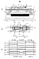
本発明のMEMSスイッチの第1の実施形態について、図1を用いて説明する。図1(a)は本発明のMEMSスイッチ部の断面構造、図1(b)はMEMSスイッチの平面図である。図1(a)は図1(b)のD−D’における断面構造に相当する。該MEMSスイッチは2つのスイッチで構成されている。本実施形態では前段のスイッチS1をホットスイッチ、後段のスイッチS2をコールドスイッチで作製している。
ホットスイッチS1では、キャパシタの2つの電極となる可動電極116、固定電極118の間に電位差を与えたときに、可動電極116が固定電極118に引きつけられ固定接点120に短絡し、ON動作となる。後段のコールドスイッチS2では、可動電極117と可動接点109との間に絶縁膜110が挟まれている。ホットスイッチと同様に、キャパシタの2つの電極となる可動電極117と固定電極119の間に電位差を与えると、可動電極117が固定電極119に引きつけられることになるが、可動接点109が可動電極117と絶縁されているので、可動接点109で2つの固定接点(配線)Y1,Y2を短絡させて、信号を伝達することになる。この動作を図1(b)の平面図と図1(c)のタイミングチャートで説明する。
<
A first embodiment of a MEMS switch according to the present invention will be described with reference to FIG. FIG. 1A is a cross-sectional structure of a MEMS switch portion of the present invention, and FIG. 1B is a plan view of the MEMS switch. FIG. 1A corresponds to a cross-sectional structure taken along the line DD ′ in FIG. The MEMS switch is composed of two switches. In the present embodiment, the front-stage switch S1 is made of a hot switch and the rear-stage switch S2 is made of a cold switch.
In the hot switch S1, when a potential difference is applied between the
スイッチS2をON動作させるときは、スイッチS1の可動電極端子A2を+Vcc、スイッチS1の固定電極端子A1をGND、スイッチS2の固定電極端子B1をGNDとする。スイッチS1の可動電極116と固定電極118の電位差が|Vcc|となり、スイッチS1はON状態となって可動電極116と固定接点120とが短絡される。スイッチS1がON状態でA2が+Vccとなっているので、スイッチS2の可動電極117の電位B2も+Vccとなり、スイッチS2の可動電極117と固定電極119間の電位差も|Vcc|となり、スイッチS2もON状態となる。このとき、スイッチS2の可動接点109が2つの配線端子(固定接点)Y1,Y2間をショートしY1=Y2となる。
その後、スイッチS1の可動電極端子A2をGNDにすると、スイッチS1はOFF状態となるが、スイッチS2の可動電極117には電荷が蓄積されているため、スイッチS2の固定電極119との間の電位差を維持することができ、スイッチS2はON状態を保持する。
When the switch S2 is turned on, the movable electrode terminal A2 of the switch S1 is set to + Vcc, the fixed electrode terminal A1 of the switch S1 is set to GND, and the fixed electrode terminal B1 of the switch S2 is set to GND. The potential difference between the
Thereafter, when the movable electrode terminal A2 of the switch S1 is set to GND, the switch S1 is turned off, but since the electric charge is accumulated in the
実際には、図1(c)に記載したように、スイッチS1をOFFする際に、スイッチS2の可動電極117と固定電極119間に蓄積された電荷は一部放電されてしまう。この放電電荷量が多いと、スイッチS2の可動電極117と固定電極119との電位差の低下が大きくなり、スイッチS2のON状態を保持できなくなる。そのため、スイッチS2のキャパシタの電極サイズをスイッチS1に比べて大きくし、蓄積電荷量を多くした。また、スイッチS1をOFF動作させるときには、スイッチS2の上下電極間隔(可動電極−固定電極間隔)は狭くなっているため、多少電位が低下してもON状態を保持することは可能である。
Actually, as described in FIG. 1C, when the switch S1 is turned OFF, the charge accumulated between the
次に、スイッチS1の固定電極端子A1を+Vccとすると、スイッチS1の可動電極116と固定電極118間の電位差は|Vcc|となり、スイッチS1はON状態となって可動電極116と固定接点120とが短絡する。この時、スイッチS1の可動電極端子A2がGNDであるため、スイッチS2の可動電極117の電位B2もGNDとなり、スイッチS2の固定電極119と同電位になるため、スイッチS2のキャパシタに蓄積された電荷は放電され、スイッチS2はOFF状態となる。
図1(a)に示したように、ホットスイッチS1の各端子A1,A2には電位供給回路C1のMOSトランジスタT1が接続される。同様に、コールドスイッチS2の固定接点端子Y1,Y2にも、スイッチング対象回路C2のMOSトランジスタT2が接続される。
Next, assuming that the fixed electrode terminal A1 of the switch S1 is + Vcc, the potential difference between the
As shown in FIG. 1A, the MOS transistor T1 of the potential supply circuit C1 is connected to the terminals A1 and A2 of the hot switch S1. Similarly, the MOS transistor T2 of the switching target circuit C2 is also connected to the fixed contact terminals Y1 and Y2 of the cold switch S2.
ホットスイッチS1を介さずにコールドスイッチS2のON−OFF制御をMOSトランジスタのスイッチ動作で実現することも理論的上は出きるが、現実的にはMOSトランジスタではOFF時のリーク電流により、コールドスイッチS2の蓄積電荷が徐々に放電されてON状態の保持が不可能である。そのため、本発明では物理的に電位供給回路を切り離すことができるMEMSスイッチS1を用いることで、ON状態の保持を確実に実行可能なものとしている。
また、上述の説明では、コールドスイッチS2の固定電極B1をGNDとし、可動電極B2に+Vccを与えることで、キャパシタの各電極間の電位差を|Vcc|としたが、固定電極B1に+Vcc、可動電極B2にGNDを与えることによって、各電極間の電位差を|Vcc|としてもスイッチS2のON動作,ON状態保持は可能である。この場合には、固定電極B1を電位供給回路C1に直接接続すると電位供給回路C1のMOSトランジスタのOFF時のリーク電流によってスイッチS2のON状態保持が不可能となってしまうため、図1(a),(b)でスイッチS2の可動電極117に接続されているスイッチS1の固定接点120をスイッチS2の固定電極119に接続する。
Although it is theoretically possible to realize the ON / OFF control of the cold switch S2 by the switching operation of the MOS transistor without using the hot switch S1, in reality, in the MOS transistor, the cold switch is caused by the leakage current at the OFF time. The accumulated charge of S2 is gradually discharged, and the ON state cannot be maintained. Therefore, in the present invention, by using the MEMS switch S1 that can physically disconnect the potential supply circuit, the ON state can be reliably held.
In the above description, the fixed electrode B1 of the cold switch S2 is set to GND, and + Vcc is applied to the movable electrode B2, so that the potential difference between the respective electrodes of the capacitor is | Vcc |. By applying GND to the electrode B2, the switch S2 can be turned on and maintained even if the potential difference between the electrodes is | Vcc |. In this case, if the fixed electrode B1 is directly connected to the potential supply circuit C1, the ON state of the switch S2 cannot be maintained due to the leakage current when the MOS transistor of the potential supply circuit C1 is OFF. ), (B), the fixed
なお、上述のコールドスイッチS2では、スイッチング対象回路C2に繋がる2つの固定接点Y1,Y2を設け、可動接点109で各固定接点Y1,Y2間を短絡させるものとなっているが、図2に示すようにコールドスイッチS2の固定接点を1つとし、固定接点Y2と可動接点Y1をスイッチング対象回路C2に接続することも可能である。但し、図2のコールドスイッチS2では固定接点の電気的引出しのためにコールドスイッチS2の可動部の重心と駆動力中心のアンバランスが発生する為、コールドスイッチの設計上は図1(b)のコールドスイッチS2の如き構成の方が好ましい。
次に、本実施形態のMEMSスイッチの製造方法を説明する。
図3(a)は電位供給回路C1,スイッチング対象回路C2のトランジスタを形成したウェハの上層にMEMSスイッチを形成する途中の工程を示したものである。尚、スイッチング対象回路部は図示を省略している。層間絶縁膜101内に下層配線102が埋め込まれている。この下層配線102がプラグ103を介してトランジスタT1に接続されている。層間絶縁膜101のキャップ膜104としてSiNを堆積し、SiN104と層間絶縁膜101を開口してプラグ103を埋込、平坦化した後にスイッチの固定電極や固定接点となる下層導電膜105を堆積する。ここでは、poly−Siを用いた。その上にホトリソ工程により、固定電極や固定接点のパターンをレジスト100に転写する。このレジストをマスクにpoly−Siをエッチングし、レジストを除去する(図3(b))。
In the above-described cold switch S2, two fixed contacts Y1 and Y2 connected to the switching target circuit C2 are provided, and the fixed contacts Y1 and Y2 are short-circuited by the
Next, a method for manufacturing the MEMS switch of this embodiment will be described.
FIG. 3A shows a process in the middle of forming the MEMS switch on the upper layer of the wafer on which the transistors of the potential supply circuit C1 and the switching target circuit C2 are formed. The switching target circuit unit is not shown. A
表面を洗浄した後、スイッチのギャップとなる犠牲膜106としてプラズマTEOSを堆積し、スイッチの固定接点に対向するところを開口したパターンをホトリソ工程を通してレジスト107に転写したのが図3(c)である。
このレジストをマスクに犠牲膜に窪み108を形成し、レジストを除去した状態が図3(d)である。この窪み108を形成せずにスイッチの可動電極,可動接点を形成することもできるが、可動電極116,可動接点109の固定接点120,105と接触させる部分を凸形状にした方がスイッチの信頼性は高くなる。
引き続き、表面を洗浄し、可動接点となる導電膜99としてpoly−Siを堆積し、コールドスイッチS2側の可動接点部にのみレジストパターン98をホトリソ工程により形成した(図4(a))。
これをマスクに電極端子109をパターニングし、レジスト98を除去したものが図4(b)である。
After cleaning the surface, plasma TEOS is deposited as a
FIG. 3D shows a state in which a
Subsequently, the surface was cleaned, poly-Si was deposited as a
The
次に、コールドスイッチS2の可動接点である電極端子109と犠牲層106の表面に絶縁膜110を堆積し、更に、コールドスイッチS2の電極端子109を覆うようにレジストパターン111を形成したものが図4(c)である。本実施形態ではこの絶縁膜110にアルミナを用いた。
絶縁膜110をドライエッチング除去し、レジスト111を除去した状態が図4(d)である。
さらに、洗浄工程を通し、ホトリソ工程で可動電極の接続口をレジストパターン112で形成したものが図5(a)である。
このレジスト112をマスクに犠牲層106をエッチングし、下層導電膜105の表面まで開口113し、レジスト112を除去した状態が図5(b)である。
この開口部113と犠牲層106の表面にスイッチの可動電極として導電膜114を堆積し、可動電極のパターンをレジスト115に転写したものが図5(c)である。本実施形態では、可動電極材料をpoly−Siとした。
このレジストパターン115をマスクに可動電極となる導電膜114をエッチングし、レジスト115を除去し(図5(d))、ホットスイッチとコールドスイッチの可動電極116,117部分を形成する。
Next, an insulating
FIG. 4D shows a state where the insulating
Further, FIG. 5A shows the case where the connection port of the movable electrode is formed by the resist pattern 112 in the photolithography process through the cleaning process.
FIG. 5B shows a state in which the
FIG. 5C shows a state in which a
Using this resist
その後、犠牲層106をウェット除去し、乾燥させて図1(a)のスイッチ構造が完成する。本実施形態では、犠牲層106の除去にはフッ酸水溶液を用いた。ウェットエッチ後に水洗を行うため、そのまま乾燥させると、水の表面張力により、可動電極116,117が固定電極118,119と固着してしまうため、水洗後にメタノール洗浄を行い、最終的には、炭酸ガスの超臨界乾燥を行った。
また、図には示していないが、スイッチ構造を形成した後、ガラスやセラミックで上部を封止し、外部環境と隔離する。この際に封止内部は不活性ガスを封入するか、減圧状態にすることが望ましい。
Thereafter, the
Although not shown in the figure, after the switch structure is formed, the upper part is sealed with glass or ceramic to isolate it from the external environment. At this time, it is desirable to seal the inside of the seal with an inert gas or to reduce the pressure.
図6はスイッチの平面図の例である。図6(a)は図3(b)まで工程を進めた段階の平面図である。下部導電膜105のパターニングを行った状態に相当している。図6(b)は図5(b)の工程まで進んだ状態の平面図であり、コールドスイッチS2の電極端子(可動接点)109と、下部導電膜1105と可動電極を接続するための開口113と、下部導電膜105との配置関係を示している。図6(c)は更に可動接点109と、下部導電膜105と、開口113と、可動電極116,117の配置関係を示した図である。開口113内部は可動電極材料のpoly−Siが埋め込まれている。この図はホットスイッチS1とコールドスイッチS2を各1つずつ使用して作製したラッチ機能付きMEMSスイッチの平面図となり、その動作については、図1を用いて前記した。
<実施形態2>
この他に、ホットスイッチを2つ使用し、コールドスイッチのラッチ機能を実現した本発明の第2の実施形態について説明する。
製造プロセスは、図3〜図5と同様である。スイッチの平面図を図7に示す。前述したように、本実施形態においても、ONまたはOFF状態を保持させるためのスイッチ(図7ではS3)のキャパシタの電極サイズは、前段のスイッチ(図7ではS1,S2)のキャパシタの電極サイズよりも大きくする方が望ましい。但し、図7では同じサイズで示している。この場合でも、スイッチのON電位を|Vcc|に比べて小さくすることで安定した動作ができる。図7(a)は図3(b)まで工程を進めた段階の平面図である。下部導電膜105のパターニングを行った状態に相当している。図7(b)は図5(b)の工程まで進んだ状態の平面図であり、コールドスイッチS3の電極端子(可動接点)109と、下部導電膜105と可動電極を接続するための開口113と、下部導電膜105との配置関係を示している。図7(c)は更に可動接点109と、下部導電膜105と、開口113と、可動電極116,117の配置関係を示した図である。開口113内部は可動電極材料のpoly−Siが埋め込まれている。
FIG. 6 is an example of a plan view of the switch. FIG. 6A is a plan view of the stage where the process has been advanced to FIG. This corresponds to a state where the lower
<
In addition, a second embodiment of the present invention in which two hot switches are used and a cold switch latch function is realized will be described.
The manufacturing process is the same as that shown in FIGS. A plan view of the switch is shown in FIG. As described above, also in this embodiment, the electrode size of the capacitor of the switch (S3 in FIG. 7) for maintaining the ON or OFF state is the electrode size of the capacitor of the preceding switch (S1, S2 in FIG. 7). It is desirable to make it larger. However, the same size is shown in FIG. Even in this case, stable operation can be achieved by making the ON potential of the switch smaller than | Vcc |. FIG. 7A is a plan view of the stage where the process has been advanced to FIG. This corresponds to a state where the lower
ホットスイッチS1、S2と、コールドスイッチS3を用いた、ラッチ機能付きMEMSスイッチの動作は図8のタイミングチャートで行った。ホットスイッチS1の可動電極端子A2をGNDとし、固定電極端子A1を+Vccに設定すると、スイッチS1はON状態となり、コールドスイッチS3の固定電極の電位C1がGND電位となる。ホットスイッチS2の方は、固定電極端子B1をGNDとし、可動電極端子B2を+Vccに設定し、スイッチS2をON状態にすると、コールドスイッチS3の可動電極117の電位C2が+Vccに設定される。この状態で、コールドスイッチS3の可動電極C1と固定電極C2間には|Vcc|の電位差が生じるため、コールドスイッチS3がON状態になり、可動接点109を介して信号端子(固定接点)Y1とY2がショートされ、Y1=Y2となる。
この状態から固定電極端子A1及び可動電極端子B2をGND電位に切換えてホットスイッチS1,S2をOFFしても、コールドスイッチS3の可動電極C1と固定電極C2間には電荷が蓄積されるため、静電引力が働き続け、コールドスイッチS3はON状態を保持することが出来る。この場合も、実際にはホットスイッチS1,S2をOFFする際に、コールドスイッチS3の可動電極C2の電荷が一部放電され、可動電極C1−固定電極C2の電位差は|Vcc|より低くなるが、スイッチのON電位を保持することは出来ている。
The operation of the MEMS switch with a latch function using the hot switches S1 and S2 and the cold switch S3 was performed according to the timing chart of FIG. When the movable electrode terminal A2 of the hot switch S1 is set to GND and the fixed electrode terminal A1 is set to + Vcc, the switch S1 is turned on, and the potential C1 of the fixed electrode of the cold switch S3 becomes the GND potential. In the case of the hot switch S2, when the fixed electrode terminal B1 is set to GND, the movable electrode terminal B2 is set to + Vcc, and the switch S2 is turned on, the potential C2 of the
Even if the fixed electrode terminal A1 and the movable electrode terminal B2 are switched to the GND potential and the hot switches S1 and S2 are turned off from this state, charges are accumulated between the movable electrode C1 and the fixed electrode C2 of the cold switch S3. The electrostatic attractive force continues to work, and the cold switch S3 can maintain the ON state. Also in this case, when the hot switches S1 and S2 are actually turned off, the charge of the movable electrode C2 of the cold switch S3 is partially discharged, and the potential difference between the movable electrode C1 and the fixed electrode C2 is lower than | Vcc |. The ON potential of the switch can be held.
コールドスイッチS3をOFFする場合は、スイッチS1の固定電極端子A1に+Vcc、可動電極端子A2をGND、スイッチS2の固定電極端子B1に+Vcc、可動電極端子B2をGNDとすることで、各ホットスイッチS1,S2をON状態にするが、コールドスイッチS3の固定電極C1と可動電極C2ともにGND電位となるため、蓄積された電荷が放電され、コールドスイッチS3はOFF状態となる。尚、コールドスイッチS3がオンを保持している状態において固定電極C1はGND電位となっている為、図8中の破線に示すように必ずしもホットスイッチS1をON状態としなくても、ホットスイッチS2のみを上記電圧印加条件でONさせることによってもコールドスイッチS3をOFFすることができる。 When the cold switch S3 is turned off, each hot switch is set by setting + Vcc to the fixed electrode terminal A1 of the switch S1, GND to the movable electrode terminal A2, + Vcc to the fixed electrode terminal B1 of the switch S2, and GND to the movable electrode terminal B2. Although S1 and S2 are turned on, since both the fixed electrode C1 and the movable electrode C2 of the cold switch S3 are at the GND potential, the accumulated charge is discharged and the cold switch S3 is turned off. Since the fixed electrode C1 is at the GND potential in a state where the cold switch S3 is kept on, the hot switch S2 does not necessarily have to be turned on as shown by the broken line in FIG. The cold switch S3 can also be turned OFF by turning ON only under the above voltage application conditions.
上述の第1の実施形態は、2つのスイッチで構成しているため本実施形態より面積を縮小することができる。これに対して、本実施の形態では、コールドスイッチS3のオン状態の保持時に固定電極をも完全なフローティングとするので、上述の第1の実施形態よりもコールドスイッチS3のON状態の保持をより確実なものとすることができる。
尚、本実施の形態においても、コールドスイッチS3を、図2に示すコールドスイッチS2のように固定接点を1つとし、固定接点と可動接点をスイッチング対象回路に接続する構成とすることが可能である。
<実施形態3>
第1,第2の実施形態で、ホットスイッチとコールドスイッチを組み合わせて作製したラッチ機能付きMEMSスイッチについて説明したが、同様の機能をコールドスイッチの組合せでも実現できる。その本発明の第3の実施形態を以下説明する。
図9は3つのコールドスイッチS1,S2,S3を用いてラッチ機能付きMEMSスイッチを構成した例である。(b)に平面図を示す。(a)の断面構造図は平面図(b)のD−D’断面を示している。(c)がラッチ機能を示すタイミングチャート図である。本構成では、スイッチS3をラッチ機能付きスイッチとし、スイッチS3がON状態のときに、可動接点215を介して2つの信号端子(固定接点)Y1とY2をショート(Y1=Y2)とし、スイッチS3がOFF状態のときに信号端子Y1とY2は切離し状態となる。このコールドスイッチを直列に接続したMEMSスイッチの製造方法については後述する。図9(a)に示したように、コールドスイッチS1〜S3の可動電極220と電極端子(可動接点)212は絶縁膜215で電気的に絶縁されている。固定電極221と可動電極220の電位差が|Vcc|以上のときに、該電極間の静電力によりスイッチがONとなる様に設計した。スイッチの動作は以下の通りである。
Since the first embodiment described above is composed of two switches, the area can be reduced as compared with the present embodiment. On the other hand, in the present embodiment, the fixed electrode is also completely floating when the cold switch S3 is kept in the on state, and therefore, the cold switch S3 is more kept in the on state than in the first embodiment. It can be certain.
Also in the present embodiment, the cold switch S3 can be configured to have one fixed contact and connect the fixed contact and the movable contact to the switching target circuit as in the cold switch S2 shown in FIG. is there.
<
In the first and second embodiments, the MEMS switch with a latch function manufactured by combining a hot switch and a cold switch has been described, but the same function can be realized by a combination of cold switches. The third embodiment of the present invention will be described below.
FIG. 9 shows an example in which a MEMS switch with a latch function is configured using three cold switches S1, S2, and S3. (B) shows a plan view. The cross-sectional structure diagram of (a) shows the DD ′ cross-section of the plan view (b). FIG. 6C is a timing chart illustrating a latch function. In this configuration, the switch S3 is a switch with a latch function, and when the switch S3 is in the ON state, the two signal terminals (fixed contacts) Y1 and Y2 are short-circuited (Y1 = Y2) via the
スイッチS1の固定電極端子A1をGND、可動電極端子A2を+Vccに設定すると、スイッチS1はON状態となり、スイッチS1先端の可動接点212が端子X1とスイッチS3の固定電極端子C1を接続して同電位とする。端子X1はGNDに設定されているので、スイッチS3の固定電極221もGNDに設定される。スイッチS2についても、固定電極端子B1をGND、可動電極端子B2を+Vccに設定することで、ON状態となり、スイッチS2先端の可動接点212が、スイッチS3の可動電極端子C2を端子X2とショートさせ、両者を同電位にする。この状態で、端子X2を+Vccに設定すると、スイッチS3の可動電極220と固定電極221間に|Vcc|の電位差が生じるためスイッチS3がON状態となり、スイッチS3先端の可動接点212が信号端子(固定接点)Y1とY2をショートさせる。
この状態から、スイッチS1の可動電極端子A2とスイッチS2の可動電極端子B2をGNDに設定し、スイッチS1およびスイッチS2をOFF状態にしても、スイッチS3の可動電極220−固定電極221間には電荷が蓄積されているため、静電力は維持され、スイッチS3のON状態を保持することができる。尚、スイッチS3がONの保持状態となった後に、端子X1はGND電位に設定する。
When the fixed electrode terminal A1 of the switch S1 is set to GND and the movable electrode terminal A2 is set to + Vcc, the switch S1 is turned on, and the
From this state, even if the movable electrode terminal A2 of the switch S1 and the movable electrode terminal B2 of the switch S2 are set to GND, and the switch S1 and the switch S2 are turned off, there is no gap between the
本実施形態では、コールドスイッチでスイッチS1,S2を構成したため、スイッチS1,S2をOFFするときに、スイッチS3から蓄積電荷の放電がない。そのため前述したホットスイッチとコールドスイッチとの組合せの第1,第2の実施形態に比べて、ON状態保持の信頼性の高いスイッチを作製することができる。
スイッチS3をOFFする場合は、スイッチS1の可動電極端子A2とスイッチS2の可動電極端子B2を各々+Vccに、スイッチS1の固定電極端子A1とスイッチS2の固定電極端子B1を各々GNDに設定し、スイッチS1とスイッチS2をON状態とする。さらに、端子X2をGNDに設定すれば、スイッチS3の可動電極220−固定電極221間に蓄積された電荷が放電される。これにより、スイッチS3の可動電極220−固定電極221間の静電力がなくなり、スイッチS3はOFFになる。
In the present embodiment, since the switches S1 and S2 are configured by cold switches, no accumulated charge is discharged from the switch S3 when the switches S1 and S2 are turned off. Therefore, compared to the first and second embodiments in which the hot switch and the cold switch are combined as described above, it is possible to manufacture a switch with high ON state retention.
When the switch S3 is turned OFF, the movable electrode terminal A2 of the switch S1 and the movable electrode terminal B2 of the switch S2 are each set to + Vcc, the fixed electrode terminal A1 of the switch S1 and the fixed electrode terminal B1 of the switch S2 are respectively set to GND, The switches S1 and S2 are turned on. Furthermore, if the terminal X2 is set to GND, the electric charge accumulated between the
図9(c)のタイミングチャートでは、スイッチS3をON状態にする際に、端子X1(固定電極端子C1)の設定電位をGNDとし、端子X2(可動電極端子C2)の設定電位を+Vccとしているが、図9(c)中に点線で示すように、各端子X1,X2(固定電極端子C1,可動電極端子C2)の設定電位を逆にしてもよい。さらに、各端子X1,X2(固定電極端子C1,可動電極端子C2)の設定電位は、GNDや+Vccでなくとも端子X1(固定電極端子C1)と端子X2(可動電極端子C2)の電位差が|Vcc|以上となる電位としてやればよい。なお、この点は、スイッチS1,S2をON状態にする際も同様である。
また、スイッチS3をOFF状態とする際に、端子X1(固定電極端子C1)及び端子X2(可動電極端子C2)の設定電位をGNDとしているが、必ずしも両者をGNDとする必要はなく、端子X1(固定電極端子C1)と端子X2(可動電極端子C2)の電位差を|Vcc|未満となるような電位を両者に設定すればよい。但し、端子X1(固定電極端子C1)及び端子X2(可動電極端子C2)の設定電位を同じ電位とすることにより、OFF状態の確実性を高めることができる。なお、この点は、スイッチS1,S2をOFF状態にする際も同様である。
In the timing chart of FIG. 9C, when the switch S3 is turned on, the set potential of the terminal X1 (fixed electrode terminal C1) is set to GND, and the set potential of the terminal X2 (movable electrode terminal C2) is set to + Vcc. However, as indicated by a dotted line in FIG. 9C, the set potentials of the terminals X1, X2 (fixed electrode terminal C1, movable electrode terminal C2) may be reversed. Furthermore, the set potential of each terminal X1, X2 (fixed electrode terminal C1, movable electrode terminal C2) is not GND or + Vcc, but the potential difference between terminal X1 (fixed electrode terminal C1) and terminal X2 (movable electrode terminal C2) is | What is necessary is just to set it as the electric potential used as Vcc | or more. This point is the same when the switches S1 and S2 are turned on.
Further, when the switch S3 is turned off, the set potential of the terminal X1 (fixed electrode terminal C1) and the terminal X2 (movable electrode terminal C2) is set to GND, but it is not always necessary to set both to GND, and the terminal X1 What is necessary is just to set a potential so that the potential difference between (fixed electrode terminal C1) and terminal X2 (movable electrode terminal C2) is less than | Vcc |. However, the certainty of the OFF state can be increased by setting the terminal X1 (fixed electrode terminal C1) and the terminal X2 (movable electrode terminal C2) to the same potential. This point is the same when the switches S1 and S2 are turned off.
図9(a)のコールドスイッチを用いたラッチ機能付きMEMSスイッチの製造方法を説明する。図3(d)までは、ホットスイッチとコールドスイッチの組合せの場合と同様である。
この後、表面を洗浄し、可動接点となる導電膜210を堆積する。本実施形態でも導電膜としてpoly−Siを用いた。ホトリソ工程で各コールドスイッチの可動接点部にレジストパターン211を形成し(図10(a))、これをマスクに電極端子212をパターニングし、レジストを除去する(図10(b))。
A method for manufacturing a MEMS switch with a latch function using the cold switch of FIG. 9A will be described. The process up to FIG. 3D is the same as the combination of the hot switch and the cold switch.
Thereafter, the surface is cleaned, and a
続いて、表面に絶縁膜213としてアルミナを堆積し、コールドスイッチの可動接点である電極端子212を覆うようにレジストパターン214を形成したものが図10(c)である。
該アルミナ絶縁膜213をドライエッチング除去し、レジスト214を除去した状態が図10(d)である。この状態では電極端子(可動接点)212はアルミナ絶縁膜215に覆われている。
さらに、洗浄工程を通し、ホトリソ工程で可動電極の接続口をレジストパターン216で形成し(図11(a))、このレジスト216をマスクに犠牲層207をエッチングし、下層導電膜205の表面まで開口217し、レジスト216を除去した状態が図11(b)である。
この表面にスイッチの可動電極となる導電膜218としてpoly−Siを堆積し、可動電極のパターンをレジスト219に転写したものが図11(c)である。
このレジストパターン219をマスクに可動電極となる導電膜218をエッチングし、レジスト219を除去し(図11(d))、各コールドスイッチの可動電極部分220を形成する。
Subsequently, FIG. 10C shows a case where alumina is deposited on the surface as an insulating
FIG. 10D shows a state where the
Further, through the cleaning process, the connection port of the movable electrode is formed by the resist
FIG. 11C shows poly-Si deposited as a
Using this resist
その後、犠牲層207をウェット除去し、乾燥させて図9(a)のスイッチ構造が完成する。
本実施形態ではMEMSスイッチを何れもコールドスイッチとしている為、各々の構成は同一のものとすることができ、スイッチング特性の設計が容易となるという効果も有している。なお、上述の第1,第2の実施形態では、本実施形態におけるスイッチS3の可動電極220,固定電極221に電位を供給するための図10(b)の端子X1,X2を作りこむ必要が無いため、本実施形態に較べ小面積にて実現できるという効果がある。
<実施形態4>
本発明では、MEMSスイッチの可動電極と固定電極の間に電荷を蓄積し、その電荷を保持することで、両電極間の静電力を維持し、スイッチのON状態を維持することを特徴としている。ここまで説明した各実施形態では、スイッチの動作環境として、減圧環境か、不活性ガス封入した環境としているが、スイッチをON状態で保持する場合、電極表面に微弱なリーク電流が流れ、蓄積電荷量を劣化させる可能性がある。
この対策として、固定電極、可動電極表面を絶縁膜で被覆することが効果的である。その本発明の第4の実施形態を以下説明する。
図12(a)は図3(b)と同工程を示す図で、層間絶縁膜表面にSiN膜304を堆積し、poly−Si下層電極305を形成した状態を表している。
図12(b)に示すように、この表面に、アルミナ絶縁膜306を堆積し、スイッチの可動接点が接触する部分に相当するところを開口したレジストパターン307をホトリソ工程で形成する。ここで堆積したアルミナ絶縁膜306が各スイッチの固定電極表面を被覆し、表面リーク電流を抑制する。
Thereafter, the
In the present embodiment, since all the MEMS switches are cold switches, the respective configurations can be the same, and the switching characteristics can be easily designed. In the first and second embodiments described above, it is necessary to create the terminals X1 and X2 in FIG. 10B for supplying a potential to the
<Embodiment 4>
The present invention is characterized in that charges are accumulated between the movable electrode and the fixed electrode of the MEMS switch, and the electrostatic force between the two electrodes is maintained and the switch is kept in an ON state by holding the charge. . In each of the embodiments described so far, the operating environment of the switch is a reduced pressure environment or an environment filled with an inert gas. However, when the switch is held in the ON state, a weak leakage current flows on the electrode surface, and the accumulated charge There is a possibility of deteriorating the amount.
As a countermeasure, it is effective to cover the surfaces of the fixed electrode and the movable electrode with an insulating film. The fourth embodiment of the present invention will be described below.
FIG. 12A is a diagram showing the same process as FIG. 3B, and shows a state in which the
As shown in FIG. 12B, an
レジストパターン307をマスクに、絶縁膜306をエッチングして開口部308を形成し、レジスト307を除去した状態が図12(c)である。
表面を洗浄した後、スイッチのギャップとなる犠牲膜309としてプラズマTEOSを堆積し、スイッチの可動接点形成部に相当するところを開口したパターンをホトリソ工程を通してレジスト310に転写したのが図12(d)である。
このレジストをマスクに犠牲膜に窪み311を形成し、レジストを除去した状態が図13(a)である。
この後、表面を洗浄し、可動接点となる導電膜312を堆積する。本実施形態でも導電膜としてpoly−Siを用いた。ホトリソ工程で各コールドスイッチの可動接点部にレジストパターン313を形成した(図13(b))。
これをマスクにスイッチの可動接点である電極端子314をパターニングし、レジスト313を除去する(図13(c))。
FIG. 12C shows a state where the insulating
After the surface is cleaned, plasma TEOS is deposited as a
FIG. 13A shows a state in which a
Thereafter, the surface is cleaned, and a
Using this as a mask, the
続いて、表面に絶縁膜315としてアルミナを堆積し、ホトリソ工程で可動電極の接続口をレジストパターン316で形成し(図13(d))、このレジスト316をマスクにアルミナ絶縁膜315,犠牲層309,下層電極表面のアルミナ絶縁膜306を連続エッチングし、下層導電膜305の表面まで開口317し、レジスト316を除去した状態が図14(a)である。
この表面にスイッチの可動電極となる導電膜318としてpoly−Siを堆積し、可動電極のパターンをレジスト319に転写したものが図14(b)である。
このレジストパターン319をマスクに可動電極となる導電膜318とその下のアルミナ絶縁膜315をエッチングし、レジスト319を除去し(図14(c))、各コールドスイッチの可動電極部分320を形成する。
Subsequently, alumina is deposited as an insulating
FIG. 14B shows the surface in which poly-Si is deposited as the
Using this resist
その後、犠牲層309をウェット除去し、乾燥させて図14(d)のスイッチ構造が完成する。
本実施形態では、固定電極などの下層電極305の表面をアルミナ306で覆い、かつ、可動電極320下側表面をアルミナ315で覆っているため、スイッチをON状態で保持した場合の可動電極−固定電極間の表面リーク電流を低減し、スイッチの信頼性を高くすることができる。
但し、可動電極320のpoly−Siと下側表面のアルミナ315が積層しているため、膜の応力制御に注意し、可動電極320の反りを抑制する必要がある。そのため、固定電極表面のみを絶縁膜306で被覆するのが最適である。
本実施形態は上述の各実施形態と組合せることによって、ON状態保持の信頼性を更に確実なものとすることができる。
Thereafter, the
In this embodiment, since the surface of the
However, since poly-Si of the
By combining this embodiment with the above-described embodiments, the reliability of maintaining the ON state can be further ensured.
11…従来技術における基板、12…コイル、13…可動電極、14…可動電極表面の電気接点、15…可動電極表面の磁性材料、16…固定電極表面の電気接点、17固定電極表面の磁性材料、18…固定電極、21…従来技術における基板、22…下部電極、23…ダイアフラム、101…層間絶縁膜、102…下層配線、103…プラグ、104…層間絶縁膜のキャップ膜、105…下層導電膜、106…犠牲膜、107…レジスト、108…犠牲層表面の凹パターン、109…電極端子パターン、110…絶縁膜、111…レジスト、112…レジスト、113…可動電極固定部用の開口パターン、114…導電膜、115…レジスト、116…ホットスイッチ可動電極、117…コールドスイッチ可動電極、118…ホットスイッチ固定電極、119…コールドスイッチ固定電極、205…下層電極、207…犠牲層、210…導電膜、211…レジスト、212…電極端子パターン、213…絶縁膜、214…レジスト、215…電極端子被覆絶縁膜、216…レジスト、217…可動電極固定部用の開口パターン、218…導電膜、219…レジスト、220…可動電極、221…固定電極、304…層間絶縁膜のキャップ膜、305…下層導電膜、306…絶縁膜、307…レジスト、308…開口部、309…犠牲膜、310…レジスト、311…犠牲膜表面の凹パターン、312…導電膜、313…レジスト、314…電極端子パターン、315…絶縁膜、316…レジスト、317…可動電極固定部用の開口パターン、318…導電膜、319…レジスト、320…可動電極。
DESCRIPTION OF
Claims (11)
第2の固定電極と、第2の固定接点と、第2の可動電極とを有し、キャパシタの電極を構成する前記第2の固定電極と前記第2の可動電極との電位差を制御することにより前記第2の固定接点と前記第2の可動電極の接触/非接触を制御可能な第2のMEMSスイッチとを有し、A second fixed electrode, a second fixed contact, and a second movable electrode are provided, and a potential difference between the second fixed electrode and the second movable electrode constituting the capacitor electrode is controlled. And a second MEMS switch capable of controlling contact / non-contact between the second fixed contact and the second movable electrode,
前記第2の固定接点が前記第1の可動電極又は前記第1の固定電極に接続され、前記第2の固定接点と前記第2の可動電極とを接触させた後に非接触とすることにより、前記第2の固定接点から供給される電荷を、前記第1の可動電極又は前記第1の固定電極に蓄積し、前記第1の固定接点と前記可動接点の接触を保持することを特徴とする半導体装置。The second fixed contact is connected to the first movable electrode or the first fixed electrode, and the second fixed contact and the second movable electrode are brought into contact with each other, and then brought into non-contact. The charge supplied from the second fixed contact is accumulated in the first movable electrode or the first fixed electrode, and the contact between the first fixed contact and the movable contact is maintained. Semiconductor device.
前記第1の固定接点及び前記第3の固定接点がスイッチング対象の回路に接続され、The first fixed contact and the third fixed contact are connected to a circuit to be switched;
前記第1の固定電極と前記第1の可動電極の間に電位差を与えることにより、前記可動接点が前記第1の固定接点及び前記第3の固定接点に接触し、前記第1の固定接点と前記第3の固定接点間が導通状態となることを特徴とする請求項1に記載の半導体装置。By applying a potential difference between the first fixed electrode and the first movable electrode, the movable contact contacts the first fixed contact and the third fixed contact, and the first fixed contact and The semiconductor device according to claim 1, wherein the third fixed contact is in a conductive state.
前記第1の固定電極,前記第2の固定電極及び前記第2の可動電極が電位供給回路に接続され、The first fixed electrode, the second fixed electrode, and the second movable electrode are connected to a potential supply circuit;
前記第1のMEMSスイッチのオン動作時,オン状態の保持時及びオフ動作時に、前記第1の固定電極に接地電位が供給され、A ground potential is supplied to the first fixed electrode when the first MEMS switch is turned on, held in an on state, and turned off.
前記第2の固定電極に接地電位,前記第2の可動電極に第1の電位を供給することにより、前記第1のMEMSスイッチをオン動作させ、By supplying a ground potential to the second fixed electrode and a first potential to the second movable electrode, the first MEMS switch is turned on,
その後、前記第2の可動電極に接地電位を供給することにより、前記第1のMEMSスイッチをオン状態に保持し、Thereafter, by supplying a ground potential to the second movable electrode, the first MEMS switch is held in an ON state,
その後、前記第2の可動電極に接地電位,前記第2の固定電極に前記第1の電位を供給することにより、前記第1のMEMSスイッチをオフ動作させることを特徴とする請求項1に記載の半導体装置。2. The first MEMS switch is then turned off by supplying a ground potential to the second movable electrode and supplying the first potential to the second fixed electrode. Semiconductor device.
前記第2の固定接点が前記第1の可動電極に接続され、前記第3の固定接点が前記第1の固定電極に接続されていることを特徴とする請求項1に記載の半導体装置。The semiconductor device according to claim 1, wherein the second fixed contact is connected to the first movable electrode, and the third fixed contact is connected to the first fixed electrode.
前記第2の固定電極及び前記第3の可動電極に第1の電位,前記第2の可動電極及び前記第3の固定電極に第2の電位を供給することにより、前記第1のMEMSスイッチをオン動作させ、By supplying a first potential to the second fixed electrode and the third movable electrode, and supplying a second potential to the second movable electrode and the third fixed electrode, the first MEMS switch is turned on. Turn on,
その後、前記第2の可動電極及び前記第3の固定電極に前記第1の電位を供給することにより、前記第1のMEMSスイッチをオン状態に保持し、Thereafter, by supplying the first potential to the second movable electrode and the third fixed electrode, the first MEMS switch is held in an on state,
その後、前記第2の可動電極に前記第1の電位,前記第2の固定電極に前記第2の電位を供給することにより、前記第1のMEMSスイッチをオフ動作させることを特徴とする請求項5に記載の半導体装置。The first MEMS switch is then turned off by supplying the first potential to the second movable electrode and the second potential to the second fixed electrode. 5. The semiconductor device according to 5.
第2の固定電極と、第2の固定接点と、第2の可動電極と、第2の可動接点とを有し、キャパシタの電極を構成する前記第2の固定電極と前記第2の可動電極との電位差を制御することにより前記第2の固定接点と前記第2の可動接点の接触/非接触を制御可能な第2のMEMSスイッチとを有し、The second fixed electrode, the second fixed contact, the second movable electrode, and the second movable contact, and the second fixed electrode and the second movable electrode constituting the capacitor electrode A second MEMS switch capable of controlling contact / non-contact of the second fixed contact and the second movable contact by controlling a potential difference between the second fixed contact and the second MEMS contact,
前記第2の固定接点が前記第1の可動電極又は前記第1の固定電極に接続され、The second fixed contact is connected to the first movable electrode or the first fixed electrode;
前記第2の固定接点と前記第2の可動電極とを接触させた後に非接触とすることにより、前記第2の固定接点から供給される電荷を、前記第1の可動電極又は前記第1の固定電極に蓄積し、前記第1の固定接点と前記可動接点の接触を保持することを特徴とする半導体装置。The contact between the second fixed contact and the second movable electrode is made non-contact, whereby the charge supplied from the second fixed contact is changed to the first movable electrode or the first movable electrode. A semiconductor device that accumulates in a fixed electrode and holds the contact between the first fixed contact and the movable contact.
前記第1の固定接点及び前記第3の固定接点がスイッチング対象の回路に接続され、The first fixed contact and the third fixed contact are connected to a circuit to be switched;
前記第1の固定電極と前記第1の可動電極の間に電位差を与えることにより、前記第1の可動接点が前記第1の固定接点及び前記第3の固定接点に接触し、前記第1の固定接点と前記第3の固定接点間が導通状態となることを特徴とする請求項7に記載の半導体装置。By applying a potential difference between the first fixed electrode and the first movable electrode, the first movable contact comes into contact with the first fixed contact and the third fixed contact, The semiconductor device according to claim 7, wherein the fixed contact and the third fixed contact are in a conductive state.
前記第2の固定接点が前記第1の可動電極に接続され、前記第3の固定接点が前記第1の固定電極に接続されていることを特徴とする請求項7に記載の半導体装置。The semiconductor device according to claim 7, wherein the second fixed contact is connected to the first movable electrode, and the third fixed contact is connected to the first fixed electrode.
前記第2のMEMSスイッチのオン動作により、前記第2の固定接点と前記第4の固定接点とが前記第2の可動接点を介して短絡され、By the ON operation of the second MEMS switch, the second fixed contact and the fourth fixed contact are short-circuited via the second movable contact,
前記第3のMEMSスイッチのオン動作により、前記第3の固定接点と前記第5の固定接点とが前記第3の可動接点を介して短絡され、By the ON operation of the third MEMS switch, the third fixed contact and the fifth fixed contact are short-circuited via the third movable contact,
前記第2の固定電極,前記第2の可動電極,前記第3の固定電極、前記第3の可動電極,前記第4の固定接点,前記第5の固定接点が電位供給回路に接続され、The second fixed electrode, the second movable electrode, the third fixed electrode, the third movable electrode, the fourth fixed contact, and the fifth fixed contact are connected to a potential supply circuit;
第1のMEMSスイッチがオンし得る電位差を前記第4の固定接点と前記第5の固定接点に供給し、前記第2のMEMSスイッチ及び前記第3のMEMSスイッチの各々をオンさせることにより、前記第1のMEMSスイッチをオン動作させ、By supplying a potential difference that can turn on the first MEMS switch to the fourth fixed contact and the fifth fixed contact, and turning on each of the second MEMS switch and the third MEMS switch, Turning on the first MEMS switch;
その後、前記第2のMEMSスイッチ及び前記第3のMEMSスイッチの各々をオフさせることにより、前記第1のMEMSスイッチをオン状態に保持し、Thereafter, by turning off each of the second MEMS switch and the third MEMS switch, the first MEMS switch is held in an ON state,
その後、第1のMEMSスイッチがオフし得る電位差を前記第4の固定接点と前記第5の固定接点に供給し、前記第2のMEMSスイッチ及び前記第3のMEMSスイッチの各々をオンさせることにより、前記第1のMEMSスイッチをオフ動作させることを特徴とする請求項10に記載の半導体装置。Thereafter, a potential difference that can be turned off by the first MEMS switch is supplied to the fourth fixed contact and the fifth fixed contact, and each of the second MEMS switch and the third MEMS switch is turned on. The semiconductor device according to claim 10, wherein the first MEMS switch is turned off.
Priority Applications (2)
| Application Number | Priority Date | Filing Date | Title |
|---|---|---|---|
| JP2003339156A JP4561072B2 (en) | 2003-09-30 | 2003-09-30 | Semiconductor device having MEMS switch |
| US10/788,369 US7045843B2 (en) | 2003-09-30 | 2004-03-01 | Semiconductor device using MEMS switch |
Applications Claiming Priority (1)
| Application Number | Priority Date | Filing Date | Title |
|---|---|---|---|
| JP2003339156A JP4561072B2 (en) | 2003-09-30 | 2003-09-30 | Semiconductor device having MEMS switch |
Publications (3)
| Publication Number | Publication Date |
|---|---|
| JP2005109071A JP2005109071A (en) | 2005-04-21 |
| JP2005109071A5 JP2005109071A5 (en) | 2006-02-09 |
| JP4561072B2 true JP4561072B2 (en) | 2010-10-13 |
Family
ID=34373343
Family Applications (1)
| Application Number | Title | Priority Date | Filing Date |
|---|---|---|---|
| JP2003339156A Expired - Fee Related JP4561072B2 (en) | 2003-09-30 | 2003-09-30 | Semiconductor device having MEMS switch |
Country Status (2)
| Country | Link |
|---|---|
| US (1) | US7045843B2 (en) |
| JP (1) | JP4561072B2 (en) |
Families Citing this family (12)
| Publication number | Priority date | Publication date | Assignee | Title |
|---|---|---|---|---|
| KR100803690B1 (en) * | 2006-08-10 | 2008-02-20 | 삼성전자주식회사 | Electro-mechanical non-volatile memory device and method for manufacturing the same |
| US7511994B2 (en) * | 2006-08-31 | 2009-03-31 | Micron Technology, Inc. | MEM suspended gate non-volatile memory |
| KR100781972B1 (en) * | 2006-09-18 | 2007-12-06 | 삼성전자주식회사 | Memory device and method manufacturing the same |
| DE102006061386B3 (en) * | 2006-12-23 | 2008-06-19 | Atmel Germany Gmbh | Integrated assembly, its use and method of manufacture |
| KR100842730B1 (en) | 2007-01-16 | 2008-07-01 | 삼성전자주식회사 | Multi-bit electro-mechanical memory device and method manufacturing the same |
| KR100882148B1 (en) * | 2007-06-22 | 2009-02-06 | 한국과학기술원 | Electrostatic actuator, the method of actuating the same and applicable devices using thereof |
| KR100867667B1 (en) * | 2008-04-18 | 2008-11-10 | 주식회사 엔아이씨테크 | Microstructure and method manufacturing the same |
| US8451077B2 (en) | 2008-04-22 | 2013-05-28 | International Business Machines Corporation | MEMS switches with reduced switching voltage and methods of manufacture |
| WO2011117105A2 (en) * | 2010-03-26 | 2011-09-29 | Elmos Semiconductor Ag | Micro-electromechanical device and use thereof |
| US8685778B2 (en) | 2010-06-25 | 2014-04-01 | International Business Machines Corporation | Planar cavity MEMS and related structures, methods of manufacture and design structures |
| US8436638B2 (en) | 2010-12-10 | 2013-05-07 | International Business Machines Corporation | Switch to perform non-destructive and secure disablement of IC functionality utilizing MEMS and method thereof |
| US20130299328A1 (en) * | 2012-05-14 | 2013-11-14 | Raytheon Company | Micro electro mechanical system (mems) microwave switch structures |
Citations (2)
| Publication number | Priority date | Publication date | Assignee | Title |
|---|---|---|---|---|
| JPH09199376A (en) * | 1996-01-18 | 1997-07-31 | Murata Mfg Co Ltd | Variable-capacitance capacitor |
| JPH11204013A (en) * | 1998-01-20 | 1999-07-30 | Nippon Telegr & Teleph Corp <Ntt> | Electrostatic moving contact element and logical operation device |
Family Cites Families (3)
| Publication number | Priority date | Publication date | Assignee | Title |
|---|---|---|---|---|
| EP0758128B1 (en) | 1995-08-09 | 2001-11-28 | Infineon Technologies AG | Memory device and fabrication method |
| US6124650A (en) | 1999-10-15 | 2000-09-26 | Lucent Technologies Inc. | Non-volatile MEMS micro-relays using magnetic actuators |
| US6625047B2 (en) * | 2000-12-31 | 2003-09-23 | Texas Instruments Incorporated | Micromechanical memory element |
-
2003
- 2003-09-30 JP JP2003339156A patent/JP4561072B2/en not_active Expired - Fee Related
-
2004
- 2004-03-01 US US10/788,369 patent/US7045843B2/en not_active Expired - Fee Related
Patent Citations (2)
| Publication number | Priority date | Publication date | Assignee | Title |
|---|---|---|---|---|
| JPH09199376A (en) * | 1996-01-18 | 1997-07-31 | Murata Mfg Co Ltd | Variable-capacitance capacitor |
| JPH11204013A (en) * | 1998-01-20 | 1999-07-30 | Nippon Telegr & Teleph Corp <Ntt> | Electrostatic moving contact element and logical operation device |
Also Published As
| Publication number | Publication date |
|---|---|
| JP2005109071A (en) | 2005-04-21 |
| US20050067621A1 (en) | 2005-03-31 |
| US7045843B2 (en) | 2006-05-16 |
Similar Documents
| Publication | Publication Date | Title |
|---|---|---|
| JP4561072B2 (en) | Semiconductor device having MEMS switch | |
| JP4489651B2 (en) | Semiconductor device and manufacturing method thereof | |
| CN101116174B (en) | Wafer bonded mos decoupling capacitor | |
| JP2010129371A (en) | Switch and esd protection element | |
| WO2006120810A1 (en) | Switching element | |
| TW201440192A (en) | MEMS structures | |
| JP2006210250A (en) | Microswitching element | |
| JP2002334645A (en) | Mems relay and manufacturing method of the same | |
| CN1979715A (en) | Switch using micro electro mechanical system | |
| US8537605B2 (en) | Nonvolatile semiconductor memory device having coplanar surfaces at resistance variable layer and wiring layer and manufacturing method thereof | |
| JP5135797B2 (en) | Switching element, switching element manufacturing method, rewritable logic integrated circuit, and memory element | |
| WO2004059726A1 (en) | Integrated antifuse structure for finfet and cmos devices | |
| TW413943B (en) | Self aligned contact pad in a semiconductor device and method for forming thereof | |
| CN107579056A (en) | Array base-plate structure and display device | |
| US9287050B2 (en) | MEMS and method of manufacturing the same | |
| KR20100030735A (en) | Piezoelectric transistor and method thereof | |
| US6750078B2 (en) | MEMS switch having hexsil beam and method of integrating MEMS switch with a chip | |
| US20070116406A1 (en) | Switch | |
| US7897996B2 (en) | Semiconductor device and method for manufacturing the same | |
| US8151444B2 (en) | Method for manufacturing connecting device for randomly connecting a number of transmitters and receivers | |
| CN104241034B (en) | Micro-electro-mechanical system (mems) structure and design structures | |
| JPWO2006070681A1 (en) | Switching element and rewritable logic integrated circuit | |
| US7995023B2 (en) | Flat panel display and method for driving the same | |
| CN115394917A (en) | Ferroelectric switching device, preparation method, control method and three-dimensional memory | |
| CN115425143A (en) | Ferroelectric switching device, preparation method, control method and three-dimensional memory |
Legal Events
| Date | Code | Title | Description |
|---|---|---|---|
| A521 | Written amendment |
Free format text: JAPANESE INTERMEDIATE CODE: A523 Effective date: 20051215 |
|
| A621 | Written request for application examination |
Free format text: JAPANESE INTERMEDIATE CODE: A621 Effective date: 20051215 |
|
| RD01 | Notification of change of attorney |
Free format text: JAPANESE INTERMEDIATE CODE: A7421 Effective date: 20060421 |
|
| A977 | Report on retrieval |
Free format text: JAPANESE INTERMEDIATE CODE: A971007 Effective date: 20090223 |
|
| A131 | Notification of reasons for refusal |
Free format text: JAPANESE INTERMEDIATE CODE: A131 Effective date: 20091006 |
|
| A521 | Written amendment |
Free format text: JAPANESE INTERMEDIATE CODE: A523 Effective date: 20091204 |
|
| A131 | Notification of reasons for refusal |
Free format text: JAPANESE INTERMEDIATE CODE: A131 Effective date: 20100413 |
|
| A521 | Written amendment |
Free format text: JAPANESE INTERMEDIATE CODE: A523 Effective date: 20100610 |
|
| TRDD | Decision of grant or rejection written | ||
| A01 | Written decision to grant a patent or to grant a registration (utility model) |
Free format text: JAPANESE INTERMEDIATE CODE: A01 Effective date: 20100706 |
|
| A01 | Written decision to grant a patent or to grant a registration (utility model) |
Free format text: JAPANESE INTERMEDIATE CODE: A01 |
|
| A61 | First payment of annual fees (during grant procedure) |
Free format text: JAPANESE INTERMEDIATE CODE: A61 Effective date: 20100719 |
|
| FPAY | Renewal fee payment (event date is renewal date of database) |
Free format text: PAYMENT UNTIL: 20130806 Year of fee payment: 3 |
|
| FPAY | Renewal fee payment (event date is renewal date of database) |
Free format text: PAYMENT UNTIL: 20130806 Year of fee payment: 3 |
|
| LAPS | Cancellation because of no payment of annual fees |