JP4560025B2 - Magnetic random access memory and manufacturing method thereof - Google Patents
Magnetic random access memory and manufacturing method thereof Download PDFInfo
- Publication number
- JP4560025B2 JP4560025B2 JP2006269334A JP2006269334A JP4560025B2 JP 4560025 B2 JP4560025 B2 JP 4560025B2 JP 2006269334 A JP2006269334 A JP 2006269334A JP 2006269334 A JP2006269334 A JP 2006269334A JP 4560025 B2 JP4560025 B2 JP 4560025B2
- Authority
- JP
- Japan
- Prior art keywords
- insulating film
- wiring
- contact
- random access
- access memory
- Prior art date
- Legal status (The legal status is an assumption and is not a legal conclusion. Google has not performed a legal analysis and makes no representation as to the accuracy of the status listed.)
- Expired - Fee Related
Links
Images


Classifications
-
- G—PHYSICS
- G11—INFORMATION STORAGE
- G11C—STATIC STORES
- G11C11/00—Digital stores characterised by the use of particular electric or magnetic storage elements; Storage elements therefor
- G11C11/02—Digital stores characterised by the use of particular electric or magnetic storage elements; Storage elements therefor using magnetic elements
- G11C11/16—Digital stores characterised by the use of particular electric or magnetic storage elements; Storage elements therefor using magnetic elements using elements in which the storage effect is based on magnetic spin effect
- G11C11/165—Auxiliary circuits
- G11C11/1653—Address circuits or decoders
- G11C11/1657—Word-line or row circuits
-
- G—PHYSICS
- G11—INFORMATION STORAGE
- G11C—STATIC STORES
- G11C11/00—Digital stores characterised by the use of particular electric or magnetic storage elements; Storage elements therefor
- G11C11/02—Digital stores characterised by the use of particular electric or magnetic storage elements; Storage elements therefor using magnetic elements
- G11C11/16—Digital stores characterised by the use of particular electric or magnetic storage elements; Storage elements therefor using magnetic elements using elements in which the storage effect is based on magnetic spin effect
- G11C11/165—Auxiliary circuits
- G11C11/1659—Cell access
-
- G—PHYSICS
- G11—INFORMATION STORAGE
- G11C—STATIC STORES
- G11C11/00—Digital stores characterised by the use of particular electric or magnetic storage elements; Storage elements therefor
- G11C11/02—Digital stores characterised by the use of particular electric or magnetic storage elements; Storage elements therefor using magnetic elements
- G11C11/16—Digital stores characterised by the use of particular electric or magnetic storage elements; Storage elements therefor using magnetic elements using elements in which the storage effect is based on magnetic spin effect
- G11C11/165—Auxiliary circuits
- G11C11/1673—Reading or sensing circuits or methods
-
- G—PHYSICS
- G11—INFORMATION STORAGE
- G11C—STATIC STORES
- G11C11/00—Digital stores characterised by the use of particular electric or magnetic storage elements; Storage elements therefor
- G11C11/02—Digital stores characterised by the use of particular electric or magnetic storage elements; Storage elements therefor using magnetic elements
- G11C11/16—Digital stores characterised by the use of particular electric or magnetic storage elements; Storage elements therefor using magnetic elements using elements in which the storage effect is based on magnetic spin effect
- G11C11/165—Auxiliary circuits
- G11C11/1675—Writing or programming circuits or methods
-
- H—ELECTRICITY
- H10—SEMICONDUCTOR DEVICES; ELECTRIC SOLID-STATE DEVICES NOT OTHERWISE PROVIDED FOR
- H10B—ELECTRONIC MEMORY DEVICES
- H10B61/00—Magnetic memory devices, e.g. magnetoresistive RAM [MRAM] devices
- H10B61/20—Magnetic memory devices, e.g. magnetoresistive RAM [MRAM] devices comprising components having three or more electrodes, e.g. transistors
- H10B61/22—Magnetic memory devices, e.g. magnetoresistive RAM [MRAM] devices comprising components having three or more electrodes, e.g. transistors of the field-effect transistor [FET] type
Landscapes
- Engineering & Computer Science (AREA)
- Computer Hardware Design (AREA)
- Mram Or Spin Memory Techniques (AREA)
- Hall/Mr Elements (AREA)
Description
本発明は、磁気抵抗(Magneto Resistive)効果を利用した磁気ランダムアクセスメモリ(MRAM:Magnetic Random Access Memory)及びその製造方法に関する。 The present invention relates to a magnetic random access memory (MRAM) using a magnetoresistive effect and a method for manufacturing the same.
近年、新たな原理により情報を記憶するメモリが数多く提案されている。そのうちの一つに、Roy Scheuerlein et. Al.によって提案されたトンネル型磁気抵抗(TMR:Tunneling Magneto Resistive)効果を利用した磁気ランダムアクセスメモリがある(例えば、非特許文献1参照)。 In recent years, many memories for storing information based on a new principle have been proposed. One of them is a magnetic random access memory using a tunneling magnetoresistive (TMR) effect proposed by Roy Scheuerlein et. Al. (For example, see Non-Patent Document 1).
磁気ランダムアクセスメモリは、MTJ(Magnetic Tunnel Junction)素子により、“1”、“0”−情報を記憶する。MTJ素子は、2つの磁性層(強磁性層)により絶縁層(トンネルバリア)を挟んだ構造を有する。MTJ素子に記憶される情報は、2つの磁性層のスピンの向きが平行か又は反平行かによって判断される。 The magnetic random access memory stores “1”, “0” -information by an MTJ (Magnetic Tunnel Junction) element. The MTJ element has a structure in which an insulating layer (tunnel barrier) is sandwiched between two magnetic layers (ferromagnetic layers). Information stored in the MTJ element is determined by whether the spin directions of the two magnetic layers are parallel or antiparallel.
MTJ素子に書き込まれたデータを読み出す場合、このMTJ素子に直列にスイッチ素子を接続し、選択されたリードワード線に接続されるスイッチ素子のみをオン状態として電流経路を作る。その結果、選択されたMTJ素子のみに電流が流れるため、そのMTJ素子のデータを読み出すことができる。 When reading data written in the MTJ element, a switch element is connected in series to the MTJ element, and only the switch element connected to the selected read word line is turned on to create a current path. As a result, a current flows only through the selected MTJ element, so that data of the MTJ element can be read.
スイッチ素子としてMOSFETを用いた場合、MTJ素子の短辺(磁化困難軸方向の幅)をF(Feature size)、長辺(磁化容易軸方向の幅)を2Fとすると、セルサイズは12F2となる。従って、磁気ランダムアクセスメモリのセルサイズは、DRAMやフラッシュメモリに対して大きい。そこで、容易軸書き込みのビット線をMTJ素子の下部に配置して、かつMTJ素子の下部電極とこの下部電極のコンタクトのフリンジをセルファラインにすれば、セルサイズは10F2となる。しかしながら、セルサイズの微細化がまだ不十分であった。
本発明は、セルサイズの微細化を図ることが可能な磁気ランダムアクセスメモリ及びその製造方法を提供する。 The present invention provides a magnetic random access memory capable of reducing the cell size and a method for manufacturing the same.
本発明の第1の視点による磁気ランダムアクセスメモリは、第1の書き込み電流が流れる第1の配線と、前記第1の配線の上方に前記第1の配線と離間して設けられ、第2の書き込み電流が流れる第2の配線と、前記第1及び第2の配線間に配置され、前記第1の配線の上面に接して配置され、固定層と前記第1及び第2の書き込み電流の少なくとも一方によって磁化の向きが変わる記録層と前記固定層及び前記記録層との間に設けられた非磁性層とを有する磁気抵抗効果素子と、前記磁気抵抗効果素子上に配置され、前記磁気抵抗効果素子と積層して一体に形成された金属層と、前記金属層、前記磁気抵抗効果素子及び前記第1の配線の側面に設けられた第1のサイド絶縁膜と、前記第1のサイド絶縁膜の側面と接して形成された第1のコンタクトと、前記金属層及び前記第1のコンタクト上に配置され、前記磁気抵抗効果素子と前記第1のコンタクトとを電気的に接続する第3の配線と、前記第1のサイド絶縁膜を介して、前記金属層、前記磁気抵抗効果素子及び前記第1の配線を覆う層間絶縁膜と、を具備し、前記第1のサイド絶縁膜の材料は、前記層間絶縁膜の材料と異なる。 A magnetic random access memory according to a first aspect of the present invention is provided with a first wiring through which a first write current flows, a first wiring above the first wiring, and spaced apart from the first wiring . A second wiring through which a write current flows and the first and second wirings are disposed in contact with an upper surface of the first wiring, and a fixed layer and at least one of the first and second write currents A magnetoresistive effect element having a recording layer whose magnetization direction changes depending on one side and a nonmagnetic layer provided between the fixed layer and the recording layer; and the magnetoresistive effect element disposed on the magnetoresistive effect element. A metal layer formed integrally with the element; a first side insulating film provided on a side surface of the metal layer, the magnetoresistive effect element, and the first wiring; and the first side insulating film. The first core formed in contact with the side surface of Tact, disposed on the metal layer and the first on the contact, through the third and the wiring, the first side insulating film for electrically connecting the first contacts and the magnetoresistive element An interlayer insulating film covering the metal layer, the magnetoresistive effect element, and the first wiring, and a material of the first side insulating film is different from a material of the interlayer insulating film.
本発明の第2の視点による磁気ランダムアクセスメモリの製造方法は、半導体基板上にスイッチング素子を形成する工程と、前記スイッチング素子の上方に、第1の書き込み電流が流れる第1の配線を形成する工程と、前記第1の配線上に、固定層と記録層と前記固定層及び前記記録層との間に設けられた非磁性層とを有する磁気抵抗効果素子を形成する工程と、前記磁気抵抗効果素子上に金属層を形成する工程と、前記第1の配線、前記磁気抵抗効果素子及び前記金属層の側面に第1のサイド絶縁膜を形成する工程と、前記金属層を覆い、前記第1のサイド絶縁膜の材料とは異なる材料が用いられる第1の層間絶縁膜を形成する工程と、前記第1の層間絶縁膜を平坦化し、前記金属層を露出させる工程と、前記第1のサイド絶縁膜の一部を露出するコンタクトホールを形成する工程と、前記コンタクトホール内に前記スイッチング素子に接続する第1のコンタクトを形成する工程と、前記第1のコンタクト及び前記金属層上に第2の配線を形成し、前記第2の配線で前記金属層と前記スイッチング素子とを電気的に接続する工程と、前記第2の配線上に第2の層間絶縁膜を形成する工程と、前記第2の層間絶縁膜上に、第2の書き込み電流が流れる第3の配線を形成する工程とを具備する。 In the method of manufacturing a magnetic random access memory according to the second aspect of the present invention, a step of forming a switching element on a semiconductor substrate and a first wiring through which a first write current flows are formed above the switching element. Forming a magnetoresistive effect element having a fixed layer, a recording layer, and a nonmagnetic layer provided between the fixed layer and the recording layer on the first wiring; and the magnetoresistance forming a metal layer on effect element, the first wiring, forming a first side insulating film on the side surfaces of the magnetoresistive element and the metal layer covers the metal layer, the second A step of forming a first interlayer insulating film using a material different from the material of the first side insulating film, a step of planarizing the first interlayer insulating film and exposing the metal layer, Part of the side insulating film Forming a contact hole to be exposed; forming a first contact connected to the switching element in the contact hole; forming a second wiring on the first contact and the metal layer; Electrically connecting the metal layer and the switching element by the second wiring; forming a second interlayer insulating film on the second wiring; and on the second interlayer insulating film And forming a third wiring through which the second write current flows .
本発明によれば、セルサイズの微細化を図ることが可能な磁気ランダムアクセスメモリ及びその製造方法を提供できる。 ADVANTAGE OF THE INVENTION According to this invention, the magnetic random access memory which can achieve size reduction of a cell size, and its manufacturing method can be provided.
本発明の実施の形態を以下に図面を参照して説明する。この説明に際し、全図にわたり、共通する部分には共通する参照符号を付す。 Embodiments of the present invention will be described below with reference to the drawings. In the description, common parts are denoted by common reference symbols throughout the drawings.
[1]第1の実施形態
[1−1]磁気ランダムアクセスメモリの基本例
図1は、本発明の第1の実施形態に係る磁気ランダムアクセスメモリの基本例の断面図を示す。図2(a)は、本発明の第1の実施形態に係るMTJ素子の周辺の平面図を示す。図2(b)は、本発明の第1の実施形態に係るゲート電極の周辺の平面図を示す。以下に、第1の実施形態に係る磁気ランダムアクセスメモリの基本例について説明する。
[1] First Embodiment [1-1] Basic Example of Magnetic Random Access Memory FIG. 1 is a sectional view of a basic example of a magnetic random access memory according to the first embodiment of the present invention. FIG. 2A is a plan view of the periphery of the MTJ element according to the first embodiment of the present invention. FIG. 2B is a plan view of the periphery of the gate electrode according to the first embodiment of the present invention. A basic example of the magnetic random access memory according to the first embodiment will be described below.
図1に示すように、半導体基板11上にゲート絶縁膜12を介してゲート電極13が形成されている。このゲート電極13の両側の半導体基板11内にはソース・ドレイン拡散層15が形成され、スイッチング素子としてのMOS(Metal Oxide Semiconductor)トランジスタTrが形成されている。ここで、ゲート電極13の側面にはサイド絶縁膜16が形成され、ゲート電極13の上面にはトップ絶縁膜14が形成されている。ゲート電極13は、読み出しワード線RWLとして機能する。
As shown in FIG. 1, a
ソース・ドレイン拡散層15にはコンタクト18が接続されている。このコンタクト18は、ゲート電極13及びサイド絶縁膜16と自己整合的に形成されている。従って、コンタクト18は、サイド絶縁膜16の側面と直接接している。コンタクト18の一部は、サイド絶縁膜16上に乗り上げている。
A
ゲート電極13の上方にはビット線BLが形成されている。このビット線BL上にMTJ素子MTJが形成されている。このMTJ素子MTJ上に例えば導電性のハードマスクHM(金属層)がMTJ素子MTJと積層で一体に形成されている。ハードマスクHMの平面形状は、例えばMTJ素子MTJの平面形状と同じである。MTJ素子MTJの磁化容易軸方向の側面は、ハードマスクHM及びビット線BLの側面と一致している。ハードマスクHMの前記側面、MTJ素子MTJの磁化容易軸方向の前記側面及びビット線BLの前記側面には、サイド絶縁膜24が形成されている。
A bit line BL is formed above the
ハードマスクHM上には配線27が形成されている。この配線27の下にはコンタクト26が形成されている。コンタクト26は、ハードマスクHM、MTJ素子MTJ、ビット線BL及びサイド絶縁膜24と自己整合的に形成されている。従って、コンタクト26は、サイド絶縁膜24の側面と直接接している。コンタクト26の一部は、サイド絶縁膜24上に乗り上げている。配線27における磁化容易軸方向の一方の側面はコンタクト26の側面と一致し、他方の側面はサイド絶縁膜24の側面と一致している。そして、配線27と離間して、MTJ素子MTJの上方には書き込みワード線WWLが形成されている。
A
ハードマスクHMの材料は、例えば、酸化されても導電性を有する金属(例えば、Ru)、酸化されても比較的安定した導電性を有する高融点金属(例えば、Ta、Ti、W)、耐酸化性に優れた高融点金属化合物(例えば、TiN、TaN、WN)などが望ましい。 The material of the hard mask HM is, for example, a metal having conductivity even when oxidized (for example, Ru), a refractory metal having relatively stable conductivity even when oxidized (for example, Ta, Ti, W), acid resistance, etc. A high melting point metal compound (for example, TiN, TaN, WN) or the like having excellent chemical properties is desirable.
サイド絶縁膜24の材料は、層間絶縁膜25の材料と異なることが望ましい。コンタクト26の形成時における両者のエッチング選択比を高めるためである。例えば、層間絶縁膜25をSiO2膜(シリコン酸化膜)で形成した場合、サイド絶縁膜24はSiN膜(シリコン窒化膜)又はAlxOy膜(アルミナ膜)で形成するとよい。
The material of the side
サイド絶縁膜16及びトップ絶縁膜14の材料は、層間絶縁膜17の材料と異なることが望ましい。コンタクト18の形成時におけるエッチング選択比を高めるためである。例えば、層間絶縁膜17をSiO2膜で形成した場合、サイド絶縁膜16及びトップ絶縁膜14はSiN膜又はAlxOy膜で形成するとよい。尚、サイド絶縁膜16とトップ絶縁膜14とは、材料の密着性等を鑑みると同じ材料が望ましいが、異なる材料でもよい。
The material of the
トップ絶縁膜14の膜厚Tt1は、サイド絶縁膜16の膜厚Ts1よりも厚いことが望ましい。これは、コンタクト18の形成時のエッチングによりゲート電極13の上端部等が削れることを、トップ絶縁膜14で十分に防止するためである。
The film thickness Tt1 of the top
トップ絶縁膜14の膜厚Tt1とサイド絶縁膜16の膜厚Ts1との関係は、例えば、Tt1×1/3≦Ts1≦Tt1×1/2を満たすことが望ましい。ここで、下限値は、主にコンタクト18の形成時のエッチング選択比と絶縁耐圧とに基づいて規定される。上限値は、コンタクト18の形成時のエッチングの際、コンタクトホールの最低限の幅(特にコンタクトホールホールのサイドの幅)が確保できるように規定される。
The relationship between the film thickness Tt1 of the top
サイド絶縁膜16の膜厚は、例えば10nmから50nm程度である。サイド絶縁膜24の膜厚は、例えば10nmから50nm程度である。このサイド絶縁膜16、24の膜厚は、エッチング時のダメージ吸収と絶縁耐圧により調整される。
The film thickness of the
図3乃至図9は、本発明の第1の実施形態に係る磁気ランダムアクセスメモリの基本例の製造工程の断面図を示す。以下に、第1の実施形態に係る磁気ランダムアクセスメモリの基本例の製造方法について説明する。 3 to 9 are sectional views showing the manufacturing steps of the basic example of the magnetic random access memory according to the first embodiment of the present invention. A method for manufacturing the basic example of the magnetic random access memory according to the first embodiment will be described below.
まず、図3に示すように、半導体基板(例えばシリコン基板)11内にSTI(Shallow Trench Isolation)構造の素子分離領域STIが形成される。次に、半導体基板11上にゲート絶縁膜12が形成され、このゲート絶縁膜12上に例えばポリシリコンからなるゲート電極13が形成される。そして、このゲート電極13上にトップ絶縁膜14が形成される。このトップ絶縁膜14は、例えばSiN膜からなる。その後、ゲート絶縁膜12、ゲート電極13及びトップ絶縁膜14が所望形状にパターニングされる。そして、半導体基板11内にソース・ドレイン拡散層15が形成される。ここで、ゲート電極13は、例えば読み出しワード線RWLとして機能する。
First, as shown in FIG. 3, an element isolation region STI having an STI (Shallow Trench Isolation) structure is formed in a semiconductor substrate (for example, a silicon substrate) 11. Next, a
次に、図4に示すように、半導体基板11及びトップ絶縁膜14上にサイド絶縁膜16が形成され、このサイド絶縁膜16がゲート絶縁膜12、ゲート電極13及びトップ絶縁膜14の側面に残るようにパターニングされる。サイド絶縁膜16は、例えばSiN膜からなる。
Next, as shown in FIG. 4, a
次に、図5に示すように、半導体基板11及びトップ絶縁膜14上に例えばSiO2膜からなる層間絶縁膜17が形成される。次に、例えばRIE(Reactive Ion Etching)により層間絶縁膜17内にコンタクトホールが形成され、このコンタクトホール内を例えばW(タングステン)で埋め込むことによりコンタクト18が形成される。ここで、コンタクトホールをサイド絶縁膜16の側面を露出するように開孔することで、コンタクト18をサイド絶縁膜16及びゲート電極13と自己整合的に形成できる。
Next, as shown in FIG. 5, an
次に、図6に示すように、コンタクト18に接続する配線19が形成され、この配線19が層間絶縁膜20で埋め込まれる。そして、配線19が露出するまで層間絶縁膜20が平坦化される。次に、配線19及び層間絶縁膜20上に例えばSiO2膜からなる層間絶縁膜21が形成され、この層間絶縁膜21上に例えばAlCuからなる配線22が形成される。そして、この配線22上にMTJ素子膜23及びハードマスクHMが形成される。次に、ハードマスクHMがパターニングされた後、配線22及びMTJ素子膜23が所望形状にパターニングされる。これにより、ビット線BL及びMTJ素子MTJが形成される。
Next, as shown in FIG. 6, a
次に、図7に示すように、ビット線BL、MTJ素子MTJ及びハードマスクHMの側面にサイド絶縁膜24が形成される。このサイド絶縁膜24は、例えばSiN膜からなる。
Next, as shown in FIG. 7, the
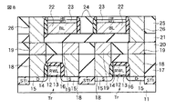
次に、図8に示すように、例えばSiO2膜からなる層間絶縁膜25が形成され、ハードマスクHMが覆われる。そして、ハードマスクHMが露出するまで層間絶縁膜25が平坦化される。その後、例えばRIEにより層間絶縁膜21、25内にコンタクトホールが形成され、サイド絶縁膜24の一部が露出される。この際、コンタクトホールの開口により、ハードマスクHMの一部が露出する場合もある。そして、コンタクトホール内を例えばWで埋め込むことにより、コンタクト26が形成される。このコンタクト26は配線19に接続される。
Next, as shown in FIG. 8, an
ここで、サイド絶縁膜24(例えばSiN膜)と層間絶縁膜25(例えばSiO2膜)とを異なる材料で形成することで、両者のエッチング選択比は高い。そして、コンタクトホールを、サイド絶縁膜24の側面を露出するように開孔し、MTJ素子MTJに隣接して形成する。これにより、コンタクト26を、サイド絶縁膜24、ビット線BL、MTJ素子MTJ及びハードマスクHMと自己整合的に形成できる。
Here, by forming the side insulating film 24 (for example, SiN film) and the interlayer insulating film 25 (for example, SiO 2 film) with different materials, the etching selectivity between them is high. Then, a contact hole is formed so as to expose the side surface of the
次に、図9に示すように、ハードマスクHM及びコンタクト26上に配線27が形成され、所望形状にパターニングされる。この配線27により、ハードマスクHMとトランジスタTrとが電気的に接続される。
Next, as shown in FIG. 9, a
最後に、図1に示すように、配線27が層間絶縁膜28で埋め込まれ、この層間絶縁膜28上に所望形状の配線29が形成される。この配線29は、書き込みワード線WWLとして機能する。
Finally, as shown in FIG. 1, the
[1−2]磁気ランダムアクセスメモリの変形例
図10は、本発明の第1の実施形態に係る磁気ランダムアクセスメモリの変形例の断面図を示す。以下に、第1の実施形態に係る磁気ランダムアクセスメモリの変形例について説明する。
[1-2] Modified Example of Magnetic Random Access Memory FIG. 10 is a sectional view of a modified example of the magnetic random access memory according to the first embodiment of the present invention. A modification of the magnetic random access memory according to the first embodiment will be described below.
図10に示すように、ハードマスクHMと配線27は、直接接していることに限定されず、コンタクト32を介して接続されていてもよい。この場合、ハードマスクHMの上面にはトップ絶縁膜31を設けておくことが望ましい。コンタクト26の形成時にハードマスクHM及びMTJ素子MTJの一部が削れることを防止するためである。
As shown in FIG. 10, the hard mask HM and the
ここで、トップ絶縁膜31とサイド絶縁膜24は、これらの周囲の層間絶縁膜21、25とエッチング選択比の高い材料が望ましい。従って、層間絶縁膜21、25が例えばSiO2膜で形成されている場合、トップ絶縁膜31とサイド絶縁膜24は例えばSiN膜又はAlxOy膜で形成するとよい。尚、トップ絶縁膜31とサイド絶縁膜24とは、材料の密着性等を鑑みると同じ材料を用いることが望ましいが、異なる材料の組み合わせでもよい。
Here, the top insulating
トップ絶縁膜31は、サイド絶縁膜24よりも厚いことが望ましい。これは、コンタクト26の形成時のエッチングによりハードマスクHM及びMTJ素子MTJの上端部等が削れることを、トップ絶縁膜31で十分に防止するためである。
The top insulating
図11及び図12は、本発明の第1の実施形態に係る磁気ランダムアクセスメモリの変形例の製造工程の断面図を示す。以下に、第1の実施形態に係る磁気ランダムアクセスメモリの変形例の製造方法について説明する。 11 and 12 are cross-sectional views showing a manufacturing process of a modification of the magnetic random access memory according to the first embodiment of the present invention. A method for manufacturing a modification of the magnetic random access memory according to the first embodiment will be described below.
まず、上述した図3乃至図5の工程を経た後、図11に示すように、コンタクト18に接続する配線19が形成され、この配線19が層間絶縁膜20で埋め込まれる。そして、配線19が露出するまで層間絶縁膜20が平坦化される。次に、配線19及び層間絶縁膜20上に層間絶縁膜21が形成され、この層間絶縁膜21上に例えばAlCuからなる配線22が形成される。この配線22上にMTJ素子膜23が形成され、このMTJ素子膜23上にハードマスクHMが形成される。そして、ハードマスクHM上にトップ絶縁膜31が形成される。このトップ絶縁膜31は、例えばSiN膜からなる。その後、配線22、MTJ素子膜23、ハードマスクHM及びトップ絶縁膜31が所望形状にパターニングされる。これにより、ビット線BL及びMTJ素子MTJが形成される。そして、ビット線BL、MTJ素子MTJ、ハードマスクHM及びトップ絶縁膜31の側面にサイド絶縁膜24が形成される。このサイド絶縁膜24は、例えばSiN膜からなる。
First, after the steps of FIGS. 3 to 5 described above, as shown in FIG. 11, a
次に、図12に示すように、例えばSiO2膜からなる層間絶縁膜25が形成される。そして、層間絶縁膜25がRIEで選択的に除去され、さらにトップ絶縁膜31がRIEで選択的に除去される。これにより、ハードマスクHMを露出するコンタクトホールが形成される。このコンタクトホールがW等で埋め込まれ、MTJ素子MTJに接続するコンタクト32が形成される。その後は、上記同様、コンタクト26、配線27、書き込みワード線WWLが順に形成される。
Next, as shown in FIG. 12, an
以上のような変形例によれば、図1の構造と同様の効果が得られるだけでなく、コンタクト32を形成することで、次のような効果も得ることができる。変形例では、MTJ素子MTJ(ハードマスクHM)と配線27との接触面積を図1の構造よりも小さくできるため、応力の影響が緩和され、磁気的に設計し易くなる。また、配線27の加工時にMTJ素子MTJに与えるエッチングダメージを抑制できる。
According to the above modification, not only the same effect as the structure of FIG. 1 can be obtained, but also the following effect can be obtained by forming the
[1−3]MTJ素子
(1)構造
図13は、本発明の第1の実施形態に係るMTJ素子の断面図を示す。以下に、MTJ素子について説明する。
[1-3] MTJ Element (1) Structure FIG. 13 is a sectional view of an MTJ element according to the first embodiment of the present invention. The MTJ element will be described below.
図13に示すように、MTJ素子MTJは、磁化が一軸方向に固定された固定層PF、磁化が反転する記録層FF、固定層PF及び記録層FFに挟まれた非磁性層NF、固定層PFの磁化を固定する反強磁性層(図示せず)を有する。 As shown in FIG. 13, the MTJ element MTJ includes a fixed layer PF whose magnetization is fixed in a uniaxial direction, a recording layer FF whose magnetization is reversed, a fixed layer PF, a nonmagnetic layer NF sandwiched between the recording layers FF, and a fixed layer. It has an antiferromagnetic layer (not shown) that fixes the magnetization of the PF.
固定層PF及び記録層FFは、図示するような単層に限定されない。例えば、固定層PF及び記録層FFは、複数の強磁性層からなる積層膜でもよい。固定層PF及び記録層FFの少なくとも一方は、第1の強磁性層/非磁性層/第2の強磁性層の3層からなり、第1及び第2の強磁性層の磁化方向が反平行状態となるように磁気結合(層間交換結合)した反強磁性結合構造であってもよいし、第1及び第2の強磁性層の磁化方向が平行状態となるように磁気結合(層間交換結合)した強磁性結合構造であってもよい。 The fixed layer PF and the recording layer FF are not limited to a single layer as illustrated. For example, the fixed layer PF and the recording layer FF may be a laminated film including a plurality of ferromagnetic layers. At least one of the fixed layer PF and the recording layer FF includes three layers of a first ferromagnetic layer / a nonmagnetic layer / a second ferromagnetic layer, and the magnetization directions of the first and second ferromagnetic layers are antiparallel. It may be an antiferromagnetic coupling structure that is magnetically coupled (interlayer exchange coupling) so as to be in a state, or magnetic coupling (interlayer exchange coupling) so that the magnetization directions of the first and second ferromagnetic layers are in a parallel state. ) Ferromagnetic coupling structure.
非磁性層NFは、図示するような1層の非磁性層からなるシングルジャンクション構造に限定されない。例えば、MTJ素子MTJは、非磁性層を2層有するダブルジャンクション構造であってもよい。このダブルジャンクション構造のMTJ素子MTJは、第1の固定層と、第2の固定層と、第1及び第2の固定層間に設けられた記録層と、第1の固定層及び記録層間に設けられた第1の非磁性層と、第2の固定層及び記録層間に設けられた第2の非磁性層とを有する。 The nonmagnetic layer NF is not limited to a single junction structure including one nonmagnetic layer as illustrated. For example, the MTJ element MTJ may have a double junction structure having two nonmagnetic layers. The MTJ element MTJ having a double junction structure includes a first fixed layer, a second fixed layer, a recording layer provided between the first and second fixed layers, and a first fixed layer and a recording layer. A first nonmagnetic layer, and a second nonmagnetic layer provided between the second fixed layer and the recording layer.
MTJ素子MTJの平面形状は、長方形に限定されない。例えば、MTJ素子MTJの平面形状は、楕円、円、六角形、菱型、平行四辺形、十字型、ビーンズ型(凹型)等種々変更可能である。但し、セルサイズの縮小の観点に鑑みれば、MTJ素子MTJの平面形状は、F(短辺)×2F(長辺)の長方形が望ましい。 The planar shape of the MTJ element MTJ is not limited to a rectangle. For example, the planar shape of the MTJ element MTJ can be variously changed such as an ellipse, a circle, a hexagon, a rhombus, a parallelogram, a cross, and a bean (concave). However, from the viewpoint of reducing the cell size, the planar shape of the MTJ element MTJ is desirably a rectangle of F (short side) × 2F (long side).
MTJ素子MTJにおける固定層PF、非磁性層NF及び記録層FFは、例えば一括加工されて同じ平面形状となっているが、これに限定されない。例えば、固定層PF及び非磁性層NFは四角形にし、記録層FFのみ十字形状にしてもよい。 The fixed layer PF, the nonmagnetic layer NF, and the recording layer FF in the MTJ element MTJ are, for example, collectively processed to have the same planar shape, but are not limited thereto. For example, the fixed layer PF and the nonmagnetic layer NF may be rectangular, and only the recording layer FF may have a cross shape.
(2)材料
固定層PF及び記録層FFの材料には、次のような強磁性材料が用いられる。例えば、Fe,Co,Ni、それらの積層膜、又はそれらの合金、スピン分極率の大きいマグネタイト、CrO2,RXMnO3−Y(R;希土類、X;Ca,Ba,Sr)等の酸化物の他、NiMnSb,PtMnSb等のホイスラー合金等を用いることが好ましい。また、これら磁性体には、強磁性を失わないかぎり、Ag,Cu,Au,Al,Mg,Si,Bi,Ta,B,C,O,N,Pd,Pt,Zr,Ir,W,Mo,Nb等の非磁性元素が多少含まれていてもよい。
(2) Material The following ferromagnetic materials are used for the material of the fixed layer PF and the recording layer FF. For example, Fe, Co, Ni, a laminated film thereof, or an alloy thereof, magnetite having a high spin polarizability, an oxide such as CrO 2 , RXMnO 3 -Y (R: rare earth, X: Ca, Ba, Sr), etc. In addition, it is preferable to use Heusler alloys such as NiMnSb and PtMnSb. In addition, these magnetic materials include Ag, Cu, Au, Al, Mg, Si, Bi, Ta, B, C, O, N, Pd, Pt, Zr, Ir, W, and Mo as long as ferromagnetism is not lost. , Nb and other nonmagnetic elements may be contained to some extent.
非磁性層NFの材料には、例えば、Al2O3,SiO2,MgO,AlN,Bi2O3,MgF2,CaF2,SrTiO2,AlLaO3等の様々な誘電体を使用することができる。これらの誘電体には、酸素、窒素、フッ素欠損が存在していてもかまわない。 For the material of the nonmagnetic layer NF, for example, various dielectrics such as Al 2 O 3 , SiO 2 , MgO, AlN, Bi 2 O 3 , MgF 2 , CaF 2 , SrTiO 2 , AlLaO 3 may be used. it can. These dielectrics may have oxygen, nitrogen, or fluorine deficiency.
ここで、非磁性層NFとしてMgO(酸化マグネシウム)、AlO(酸化アルミニウム、例えばAl2O3)等の絶縁体が用いられた場合、MTJ素子MTJはTMR(Tunneling Magneto Resistive)効果を有する。非磁性層NFとしてCu、Pt等の金属が用いられた場合、MTJ素子MTJはGMR(Giant Magneto Resistive)効果を有する。 Here, when an insulator such as MgO (magnesium oxide) or AlO (aluminum oxide, such as Al 2 O 3 ) is used as the nonmagnetic layer NF, the MTJ element MTJ has a TMR (Tunneling Magneto Resistive) effect. When a metal such as Cu or Pt is used as the nonmagnetic layer NF, the MTJ element MTJ has a GMR (Giant Magneto Resistive) effect.
(3)磁化配置
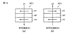
図14(a)及び(b)、図15(a)及び(b)は、本発明の第1の実施形態に係るMTJ素子の平行又は反平行の磁化配置の図を示す。
(3) Magnetization Arrangement FIGS. 14 (a) and 14 (b), 15 (a) and 15 (b) are diagrams showing parallel or antiparallel magnetization arrangements of the MTJ element according to the first embodiment of the present invention. .
図14(a)及び図15(a)に示すように、MTJ素子MTJの固定層PF及び記録層FFの磁化方向が平行(同じ向き)となった場合、非磁性層NFのトンネル抵抗は最も低くなる。この状態を、例えば“1”状態とする。 As shown in FIGS. 14A and 15A, when the magnetization directions of the fixed layer PF and the recording layer FF of the MTJ element MTJ are parallel (same direction), the tunnel resistance of the nonmagnetic layer NF is the highest. Lower. This state is, for example, a “1” state.
一方、図14(b)及び図15(b)に示すように、MTJ素子MTJの固定層PF及び記録層FFの磁化方向が反平行(逆向き)となった場合、非磁性層NFのトンネル抵抗は最も高くなる。この状態を、例えば“0”状態とする。 On the other hand, as shown in FIGS. 14B and 15B, when the magnetization directions of the fixed layer PF and the recording layer FF of the MTJ element MTJ are antiparallel (reverse), the tunnel of the nonmagnetic layer NF Resistance is highest. This state is, for example, a “0” state.
尚、固定層PF及び記録層FFの磁化の安定方向は、図14(a)及び(b)のように、膜面に対して平行な方向である平行磁化型でもよいし、図15(a)及び(b)に示すように、膜面に対して垂直な方向である垂直磁化型でもよい。 The stable directions of magnetization of the fixed layer PF and the recording layer FF may be a parallel magnetization type that is parallel to the film surface, as shown in FIGS. 14A and 14B, or FIG. ) And (b), a perpendicular magnetization type which is a direction perpendicular to the film surface may be used.
[1−4]書き込み方法
(1)磁場書き込み
書き込み方法として磁場書き込みを採用する場合、MTJ素子MTJへのデータ書き込みは次のように行われる。
[1-4] Writing Method (1) Magnetic Field Writing When magnetic field writing is adopted as a writing method, data writing to the MTJ element MTJ is performed as follows.
選択セルのMTJ素子MTJに対応するビット線BL及び書き込みワード線WWLがそれぞれ選択され、この選択されたビット線BL及び書き込みワード線WWLに書き込み電流をそれぞれ流す。この書き込み電流により発生した合成磁場をMTJ素子MTJに印加することで、MTJ素子MTJの磁化が平行又は反平行となる。 A bit line BL and a write word line WWL corresponding to the MTJ element MTJ of the selected cell are selected, and a write current is supplied to the selected bit line BL and write word line WWL. By applying a composite magnetic field generated by the write current to the MTJ element MTJ, the magnetization of the MTJ element MTJ becomes parallel or antiparallel.
例えば、書き込みワード線WWLの書き込み電流は一方向に流れ、ビット線BLの書き込み電流は両方向に流れる。この場合、ビット線BLに流れる書き込み電流の向きを変えることで、MTJ素子MTJの記録層の磁化の向きを変える。尚、書き込みワード線WWLの書き込み電流が両方向に流れてもよい。 For example, the write current of the write word line WWL flows in one direction, and the write current of the bit line BL flows in both directions. In this case, the direction of the magnetization of the recording layer of the MTJ element MTJ is changed by changing the direction of the write current flowing through the bit line BL. Note that the write current of the write word line WWL may flow in both directions.
(2)スピン注入書き込み
図14(a)及び(b)を用いて、スピン注入書き込みについて説明する。尚、電子e1、e2の流れる方向と電流の流れる方向とは勿論逆である。
(2) Spin Injection Writing Spin injection writing will be described with reference to FIGS. 14 (a) and 14 (b). Of course, the direction in which the electrons e1 and e2 flow is opposite to the direction in which the current flows.
まず、図14(a)に示すように、書き込み電流を固定層PFから記録層FFへ流すと、スピン偏極した電子(以下、スピン偏極電子と称す)e1は記録層FFから固定層PFへ流れ、固定層PFと平行なスピンを持つ電子は透過し、反平行のスピンを持つ電子が反射され、結果として、記録層FFの磁化方向と固定層PFの磁化方向が反平行磁化配置となる。 First, as shown in FIG. 14A, when a write current is passed from the fixed layer PF to the recording layer FF, spin-polarized electrons (hereinafter referred to as spin-polarized electrons) e1 are transferred from the recording layer FF to the fixed layer PF. Electrons having spins parallel to the fixed layer PF are transmitted and electrons having antiparallel spins are reflected. As a result, the magnetization direction of the recording layer FF and the magnetization direction of the fixed layer PF are antiparallel magnetization arrangements. Become.
一方、図14(b)に示すように、書き込み電流を記録層FFから固定層PFへ流すと、スピン偏極電子e2は固定層PFから記録層FFへ注入され、固定層PFの磁化方向と記録層FFの磁化方向21が平行磁化配置となる。
On the other hand, as shown in FIG. 14B, when a write current is passed from the recording layer FF to the fixed layer PF, spin-polarized electrons e2 are injected from the fixed layer PF to the recording layer FF, and the magnetization direction of the fixed layer PF The
尚、MTJ素子MTJへのデータ書き込みは、(1)磁場書き込みと(2)スピン注入書き込みとを組み合わせることも可能である。 Note that data writing to the MTJ element MTJ can be performed by combining (1) magnetic field writing and (2) spin injection writing.
[1−5]読み出し方法
MTJ素子MTJのデータ読み出しは、ビット線BLと読み出しワード線RWL間に電圧(又は電流)を印加し、電流(又は電圧)をセンスアンプ(図示せず)で検出することによって、MTJ素子MTJの“1”、“0”状態を判別する。
[1-5] Read Method For reading data from the MTJ element MTJ, a voltage (or current) is applied between the bit line BL and the read word line RWL, and the current (or voltage) is detected by a sense amplifier (not shown). Thus, the “1” and “0” states of the MTJ element MTJ are discriminated.
ここで、MTJ素子MTJの磁化配置が平行状態(例えば“1”状態)の場合は低抵抗となり、反平行状態(例えば“0”状態)の場合は高抵抗となる。従って、この抵抗値の違いを読み取ることで、MTJ素子の“1”、“0”の判別が可能である。 Here, when the magnetization arrangement of the MTJ element MTJ is in the parallel state (for example, “1” state), the resistance is low, and in the antiparallel state (for example, “0” state), the resistance is high. Therefore, it is possible to discriminate between “1” and “0” of the MTJ element by reading the difference in resistance value.
[1−6]効果
上記第1の実施形態によれば、MTJ素子MTJとスイッチング素子とをつなぐコンタクト26をビット線BL及びMTJ素子MTJに対して自己整合的に形成することで、コンタクト26がビット線BL及びMTJ素子MTJのサイド絶縁膜24と直接接する構造を実現する。つまり、MTJ素子MTJとMOSトランジスタTrとを接続するコンタクト26をMTJ素子MTJと隣接して配置でき、セルサイズを縮小できる。具体的には、図2(a)に示すように、MTJ素子MTJの短辺(磁化困難軸方向の幅)をF(Feature size)、長辺(磁化容易軸方向の幅)を2Fとすると、2F×4F=8F2のセルが実現でき、セルサイズの微細化を図ることができる。
[1-6] Effect According to the first embodiment, the
[2]第2の実施形態
第1の実施形態は、MTJ素子の横にスイッチング素子につながるコンタクトを配置したのに対し、第2の実施形態は、MTJ素子の下方にスイッチング素子につながるコンタクトを配置することで、セルサイズの更なる微細化を図っている。
[2] Second Embodiment In the first embodiment, the contact connected to the switching element is arranged beside the MTJ element, whereas in the second embodiment, the contact connected to the switching element is provided below the MTJ element. By arranging, the cell size is further miniaturized.
[2−1]磁気ランダムアクセスメモリの基本例
図16は、本発明の第2の実施形態に係る磁気ランダムアクセスメモリの基本例の断面図を示す。図17(a)は、本発明の第2の実施形態に係るMTJ素子の周辺の平面図を示す。図17(b)は、本発明の第2の実施形態に係るゲート電極の周辺の平面図を示す。以下に、第2の実施形態に係る磁気ランダムアクセスメモリの基本例について説明する。
[2-1] Basic Example of Magnetic Random Access Memory FIG. 16 is a sectional view of a basic example of a magnetic random access memory according to the second embodiment of the present invention. FIG. 17A is a plan view of the periphery of the MTJ element according to the second embodiment of the present invention. FIG. 17B is a plan view of the periphery of the gate electrode according to the second embodiment of the present invention. A basic example of the magnetic random access memory according to the second embodiment will be described below.
図16に示すように、第2の実施形態において、第1の実施形態と異なる点は、以下のようなMTJ素子MTJの周辺の構造である。 As shown in FIG. 16, the second embodiment is different from the first embodiment in the peripheral structure of the MTJ element MTJ as follows.
MOSトランジスタTrのソース・ドレイン拡散層15につながるコンタクト26上に配線27が形成され、この配線27の上面に接してMTJ素子MTJが形成されている。MTJ素子MTJは配線27と同じ平面形状を有する。MTJ素子MTJの磁化容易軸方向の側面は配線27の磁化容易軸方向の側面と一致し、MTJ素子MTJの磁化困難軸方向の側面は配線27の磁化困難軸方向の側面と一致する。MTJ素子MTJ上にはハードマスクHMが形成され、このハードマスクHM上にビット線BLが設けられている。
A
MTJ素子MTJの下方には、書き込みワード線WWLが配線27と離間して配置されている。この書き込みワード線WWLの磁化容易軸方向の側面にはサイド絶縁膜42が設けられ、書き込みワード線WWLの上面にはトップ絶縁膜41が設けられている。コンタクト26は、書き込みワード線WWL及びサイド絶縁膜42と自己整合的に形成されている。従って、コンタクト26は、サイド絶縁膜42の側面と直接接している。コンタクト26の一部は、サイド絶縁膜42上に乗り上げている。
Below the MTJ element MTJ, a write word line WWL is disposed apart from the
MOSトランジスタTrのソース・ドレイン拡散層15に接続されたコンタクト18のうちソース側のコンタクト18は、隣り合うMOSトランジスタTrで共有している。従って、隣り合うゲート電極13間の距離は、コンタクト18の幅とサイド絶縁膜16の膜厚の合計程度となる。
Of the
サイド絶縁膜42及びトップ絶縁膜41の材料は、層間絶縁膜25の材料と異なることが望ましい。コンタクト26の形成時における両者のエッチング選択比を高めるためである。例えば、層間絶縁膜25をSiO2膜で形成した場合、サイド絶縁膜42及びトップ絶縁膜41はSiN膜又はAlxOy膜で形成するとよい。尚、トップ絶縁膜41とサイド絶縁膜42とは、材料の密着性等を鑑みると同じ材料を用いることが望ましいが、異なる材料の組み合わせでもよい。
The material of the
サイド絶縁膜42の膜厚Ts2は、例えば10nm〜50nm程度である。このサイド絶縁膜42の膜厚Ts2は、トップ絶縁膜41の膜厚Tt2より薄くてもよい。例えば、Tt2×1/3≦Ts2≦Tt2×1/2を満たすことが望ましい。ここで、下限値は、主にコンタクト26の形成時のエッチング選択比と絶縁耐圧とに基づいて規定される。上限値は、コンタクト26の形成時のエッチングの際、コンタクトホールの最低限の幅(特にコンタクトホールホールのサイドの幅)が確保できるように規定される。
The film thickness Ts2 of the
図18乃至図22は、本発明の第2の実施形態に係る磁気ランダムアクセスメモリの基本例の製造工程の断面図を示す。以下に、第2の実施形態に係る磁気ランダムアクセスメモリの基本例の製造方法について説明する。 18 to 22 are sectional views showing the manufacturing steps of the basic example of the magnetic random access memory according to the second embodiment of the present invention. A method for manufacturing the basic example of the magnetic random access memory according to the second embodiment will be described below.
まず、上述した図3乃至図5の工程を経て、コンタクト18が、サイド絶縁膜16及びゲート電極13と自己整合的に形成される。
First, the
次に、図18に示すように、コンタクト18に接続する配線19が形成され、この配線19が層間絶縁膜20で埋め込まれる。そして、配線19が露出するまで層間絶縁膜20が平坦化される。次に、配線19及び層間絶縁膜20上に例えばSiO2膜からなる層間絶縁膜21が形成され、この層間絶縁膜21上に例えばAlCuからなる配線22が形成される。この配線22上には、例えばSiN膜からなるトップ絶縁膜41が形成される。その後、配線22及びトップ絶縁膜41が所望形状にパターニングされる。これにより、ビット線BLが形成される。
Next, as shown in FIG. 18, a
次に、図19に示すように、トップ絶縁膜41及び層間絶縁膜21上にサイド絶縁膜42が形成される。このサイド絶縁膜42は、例えばSiN膜からなる。
Next, as shown in FIG. 19, a
次に、図20に示すように、例えばRIEによりサイド絶縁膜42が選択的に除去され、ビット線BL及びトップ絶縁膜41の側面にサイド絶縁膜42が残される。
Next, as shown in FIG. 20, the
次に、図21に示すように、トップ絶縁膜41、サイド絶縁膜42及び層間絶縁膜21上に層間絶縁膜25が形成され、この層間絶縁膜25によりトップ絶縁膜41が覆われる。この層間絶縁膜25は、例えばSiO2膜からなる。次に、例えばCMPにより層間絶縁膜25を平坦化し、トップ絶縁膜41を露出させる。この際、トップ絶縁膜41上に層間絶縁膜25が部分的に残る場合もある。次に、例えばRIEにより層間絶縁膜21、25内にコンタクトホールが形成され、サイド絶縁膜42の一部が露出される。そして、このコンタクトホール内を例えばWで埋め込むことによりコンタクト26が形成される。このコンタクト26は配線19に接続される。
Next, as shown in FIG. 21, the
ここで、トップ絶縁膜41及びサイド絶縁膜42(例えばSiN膜)と層間絶縁膜21、25(例えばSiO2膜)とを異なる材料で形成することで、両者のエッチング選択比は高い。そして、コンタクトホールを、サイド絶縁膜42の側面を露出するように開孔し、書き込みワード線WWLに隣接して形成する。これにより、コンタクト26を、サイド絶縁膜42及び書き込みワード線WWLと自己整合的に形成できる。
Here, when the top insulating
次に、図22に示すように、コンタクト26及び層間絶縁膜25上に配線27が形成され、この配線27上にMTJ素子膜23が形成される。このMTJ素子膜23上にハードマスクHMが形成され、このハードマスクHMがパターニングされる。そして、配線27及びMTJ素子膜23が所望形状にパターニングされる。これにより、同じ平面形状を有する配線27及びMTJ素子MTJが形成される。
Next, as shown in FIG. 22, a
最後に、図16に示すように、MTJ素子MTJが層間絶縁膜28で埋め込まれ、ハードマスクHMが露出するまで層間絶縁膜28が平坦化される。次に、層間絶縁膜28及びMTJ素子MTJ上に所望形状の配線29が形成される。この配線29は、ビット線BLとして機能する。
Finally, as shown in FIG. 16, the MTJ element MTJ is embedded with the
[2−2]磁気ランダムアクセスメモリの変形例
(1)変形例1
図23は、本発明の第2の実施形態に係る磁気ランダムアクセスメモリの変形例1の断面図を示す。以下に、第2の実施形態に係る磁気ランダムアクセスメモリの変形例1について説明する。
[2-2] Modification of Magnetic Random Access Memory (1) Modification 1
FIG. 23 is a sectional view of Modification 1 of the magnetic random access memory according to the second embodiment of the present invention. A modification 1 of the magnetic random access memory according to the second embodiment will be described below.
図23に示すように、変形例1では、書き込みワード線WWLをいわゆるダマシンプロセスで形成している。このため、図16の構造ではサイド絶縁膜42は書き込みワード線WWLの側面にのみ形成されていたのに対し、図23の構造では書き込みワード線WWLの側面に形成された絶縁膜52は書き込みワード線WWLの底面にも形成されている。
As shown in FIG. 23, in the first modification, the write word line WWL is formed by a so-called damascene process. Therefore, in the structure of FIG. 16, the
そして、図23の構造では、配線の信頼性確保の観点から、書き込みワード線WWLと絶縁膜52間にバリアメタル膜53を設けることが望ましい。但し、このバリアメタル膜53は必ずしも設ける必要はない。書き込みワード線WWL、バリアメタル膜53及び絶縁膜52上にはトップ絶縁膜54が形成されている。トップ絶縁膜54の上面及びコンタクト26の上面は、配線27の底面と直接接している。
In the structure of FIG. 23, it is desirable to provide a
コンタクト26は、絶縁膜52及びビット線BLと自己整合的に形成されている。このため、コンタクト26の側面は、絶縁膜52の側面と直接接している。
The
トップ絶縁膜54と絶縁膜52は、これらの周囲の層間絶縁膜51とエッチング選択比の高い材料が望ましい。従って、層間絶縁膜51が例えばSiO2膜で形成されている場合、トップ絶縁膜54と絶縁膜52は例えばSiN膜、AlxOy膜、SiN/Ta/NiFe/Taの積層膜、FexOy膜のいずれかで形成するとよい。
The top insulating
トップ絶縁膜54は絶縁膜52よりも厚いことが望ましい。これは、コンタクト26の形成時のエッチングにより書き込みワード線WWLの上端部等が削れることを、トップ絶縁膜54で十分に防止するためである。
The top insulating
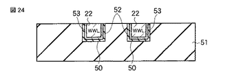
図24及び図28は、本発明の第2の実施形態に係る磁気ランダムアクセスメモリの変形例1の製造工程の断面図を示す。以下に、第2の実施形態に係る磁気ランダムアクセスメモリの変形例1の製造方法について説明する。ここでは、書き込みワード線WWLのダマシンプロセスについて説明するが、その他の製造工程は上述する第2の実施形態に係る磁気ランダムアクセスメモリの基本例の製造工程と同様である。 24 and 28 are cross-sectional views showing the manufacturing steps of Modification 1 of the magnetic random access memory according to the second embodiment of the present invention. The manufacturing method of Modification 1 of the magnetic random access memory according to the second embodiment will be described below. Here, the damascene process of the write word line WWL will be described, but other manufacturing steps are the same as those of the basic example of the magnetic random access memory according to the second embodiment described above.
まず、図24に示すように、例えばSiO2膜からなる層間絶縁膜51が例えばRIEにより選択的に除去され、層間絶縁膜51内に溝50が形成される。この溝50内及び層間絶縁膜51上に絶縁膜52が形成され、この絶縁膜52上にバリアメタル膜53が形成される。絶縁膜52は例えばSiN膜からなり、バリアメタル膜53はTaN等のTa系の材料からなる。そして、バリアメタル膜53上に例えばCuからなる配線22が形成される。その後、例えばCMPにより配線22、バリアメタル膜53及び絶縁膜52が平坦化され、層間絶縁膜51が露出される。
First, as shown in FIG. 24, the
次に、図25に示すように、配線22、バリアメタル膜53及び絶縁膜52の上部が除去され、溝50の上部に凹部55が形成される。
Next, as shown in FIG. 25, the upper portions of the
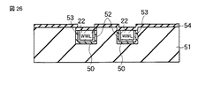
次に、図26に示すように、凹部55及び層間絶縁膜51上にトップ絶縁膜54が形成される。このトップ絶縁膜54は、例えばSiN膜からなる。
Next, as shown in FIG. 26, a top insulating
次に、図27に示すように、例えばCMPにより層間絶縁膜51上のトップ絶縁膜54が除去され、凹部55内のみにトップ絶縁膜54が残される。
Next, as shown in FIG. 27, the top insulating
次に、図28に示すように、例えばRIEにより層間絶縁膜51内にコンタクトホールが形成され、このコンタクトホール内を例えばWで埋め込むことによりコンタクト26が形成される。このコンタクト26は配線19(図示せず)に接続される。
Next, as shown in FIG. 28, a contact hole is formed in the
ここで、トップ絶縁膜54(例えばSiN膜)及び絶縁膜52(例えばSiN膜)と層間絶縁膜51(例えばSiO2膜)とを異なる材料で形成することで、両者のエッチング選択比は高い。そして、コンタクトホールを、絶縁膜52の側面を露出するように開孔し、書き込みワード線WWLに隣接して形成する。これにより、コンタクト26を、絶縁膜52及び書き込みワード線WWLと自己整合的に形成できる。
Here, by forming the top insulating film 54 (for example, SiN film) and the insulating film 52 (for example, SiN film) and the interlayer insulating film 51 (for example, SiO 2 film) with different materials, the etching selectivity between them is high. Then, a contact hole is formed so as to expose the side surface of the insulating
以上のような変形例1によれば、書き込みワード線WWLをダマシンプロセスで形成している。このため、図16と比べて、MTJ素子MTJと書き込みワード線WWLとを近づけることができる。従って、書き込みワード線WWLの書き込み電流を低減することができる。 According to Modification 1 as described above, the write word line WWL is formed by a damascene process. Therefore, compared with FIG. 16, the MTJ element MTJ and the write word line WWL can be brought closer to each other. Accordingly, the write current of the write word line WWL can be reduced.
(2)変形例2
図29は、本発明の第2の実施形態に係る磁気ランダムアクセスメモリの変形例2の断面図を示す。以下に、第2の実施形態に係る磁気ランダムアクセスメモリの変形例2について説明する。
(2)
FIG. 29 is a sectional view of
図29に示すように、ハードマスクHMとビット線BLは、直接接していることに限定されず、コンタクト62を介して接続されていてもよい。このコンタクト62は、層間絶縁膜61内にコンタクトホールを形成し、このコンタクトホール内に金属材を埋め込むことにより形成できる。
As shown in FIG. 29, the hard mask HM and the bit line BL are not limited to being in direct contact, and may be connected through a
尚、コンタクト62及びビット線BLは別々に金属材を埋め込んで形成することに限定されない。例えば、コンタクト62のコンタクトホールとビット線BLの溝を形成し、これらコンタクトホール及び溝を金属材で同時に埋め込み、コンタクト62及びビット線BLを形成することも可能である。
The
以上のような変形例2によれば、図16の構造と同様の効果が得られるだけでなく、コンタクト62を形成することで、次のような効果も得ることができる。変形例2では、MTJ素子MTJ(ハードマスクHM)とビット線BLとの接触面積を図16の構造よりも小さくできるため、応力の影響が緩和され、磁気的に設計し易くなる。また、ビット線BLの加工時にMTJ素子MTJに与えるエッチングダメージを抑制できる。
According to
[2−3]MTJ素子
第2の実施形態に係るMTJ素子MTJも、上述する第1の実施形態に係るMTJ素子MTJと同様であるため、説明は省略する。
[2-3] MTJ Element Since the MTJ element MTJ according to the second embodiment is the same as the MTJ element MTJ according to the first embodiment described above, the description thereof is omitted.
[2−4]書き込み方法
第2の実施形態に係る書き込み方法は、上述する第1の実施形態に係る書き込み方法と同様、磁場書き込み及びスピン注入書き込みのうち少なくとも一方の方法が採用される。
[2-4] Write Method As in the write method according to the first embodiment described above, at least one of magnetic field write and spin injection write is employed as the write method according to the second embodiment.
ここで、第2の実施形態は、第1の実施形態と比べて、ビット線BL及び書き込みワード線WWLの配置が異なる。 Here, the second embodiment differs from the first embodiment in the arrangement of the bit lines BL and the write word lines WWL.
第1の実施形態の場合、図2(a)に示すように、ビット線BLはMTJ素子MTJの磁化困難軸方向に延在され、書き込みワード線WWLはMTJ素子MTJの磁化容易軸方向に延在される。従って、MTJ素子MTJの磁化困難軸方向に延在する書き込み配線はビット線BLであるので、このビット線BLに流す書き込み電流がMTJ素子MTJの磁化容易軸方向に磁場を与えるため、このビット線BLの書き込み電流は両方向に流れることが望ましい。 In the case of the first embodiment, as shown in FIG. 2A, the bit line BL extends in the hard axis direction of the MTJ element MTJ, and the write word line WWL extends in the easy axis direction of the MTJ element MTJ. Be present. Accordingly, since the write wiring extending in the hard axis direction of the MTJ element MTJ is the bit line BL, the write current applied to the bit line BL applies a magnetic field in the easy axis direction of the MTJ element MTJ. It is desirable that the BL write current flow in both directions.
一方、第2の実施形態の場合、図17(a)に示すように、書き込みワード線WWLはMTJ素子MTJの磁化困難軸方向に延在され、ビット線BLはMTJ素子MTJの磁化容易軸方向に延在される。従って、MTJ素子MTJの磁化困難軸方向に延在する書き込み配線は書き込みワード線WWLであるので、この書き込みワード線WWLに流す書き込み電流がMTJ素子MTJの磁化容易軸方向に磁場を与えるため、この書き込みワード線WWLの書き込み電流は両方向に流れることが望ましい。 On the other hand, in the case of the second embodiment, as shown in FIG. 17A, the write word line WWL extends in the hard axis direction of the MTJ element MTJ, and the bit line BL extends in the easy axis direction of the MTJ element MTJ. To be extended to. Therefore, since the write wiring extending in the hard axis direction of the MTJ element MTJ is the write word line WWL, the write current flowing through the write word line WWL gives a magnetic field in the easy axis direction of the MTJ element MTJ. It is desirable that the write current of the write word line WWL flows in both directions.
[2−5]読み出し方法
第2の実施形態に係る読み出し方法は、上述する第1の実施形態に係る読み出し方法と同様であるため、説明は省略する。
[2-5] Read Method The read method according to the second embodiment is the same as the read method according to the first embodiment described above, and a description thereof will be omitted.
[2−6]効果
上記第2の実施形態によれば、MTJ素子MTJの下方の領域に、MTJ素子MTJ及びスイッチング素子をつなぐコンタクト26と書き込みワード線WWLとを配置する。そして、コンタクト26を書き込みワード線WWLに対して自己整合的に形成することで、コンタクト26が書き込みワード線WWLのサイド絶縁膜42と直接接する構造を実現する。つまり、MTJ素子MTJとMOSトランジスタTrとを接続するコンタクト26を書き込みワード線WWLと隣接して配置でき、セルサイズを縮小できる。具体的には、図17(a)に示すように、MTJ素子MTJの短辺(磁化困難軸方向の幅)をF、長辺(磁化容易軸方向の幅)を2Fとすると、2F×3F=6F2のセルが実現でき、第1の実施形態よりもセルサイズの微細化を図ることができる。
[2-6] Effect According to the second embodiment, the
[3]第3の実施形態
第3の実施形態は、上記第1及び第2の実施形態において、サイド絶縁膜等を磁性絶縁膜にする。例えば、図1及び図10のサイド絶縁膜24、図16及び図29のサイド絶縁膜42、図23の絶縁膜52の材料として、磁性絶縁材を用いる。
[3] Third Embodiment In the third embodiment, a side insulating film or the like is used as a magnetic insulating film in the first and second embodiments. For example, a magnetic insulating material is used as the material of the
この磁性絶縁材としては、例えば、絶縁性のフェライトや、(Fe、Co)−(B、Si、Hf、Zr、Sm、Ta、Al)−(F、O、N)系等の金属−非金属ナノグラニュラー膜があげられる。具体的に、絶縁性のフェライトは、例えば、Mn−Zn−フェライト、Ni−Zn−フェライト、MnFeO、CuFeO、FeO、NiFeOのうち少なくとも1つ以上の材料からなる。 Examples of the magnetic insulating material include insulative ferrite and metals such as (Fe, Co)-(B, Si, Hf, Zr, Sm, Ta, Al)-(F, O, N) -based non- An example is a metal nano granular film. Specifically, the insulating ferrite is made of, for example, at least one material of Mn—Zn—ferrite, Ni—Zn—ferrite, MnFeO, CuFeO, FeO, and NiFeO.
上記第3の実施形態によれば、第1及び第2の実施形態と同様の効果を得ることができる。 According to the third embodiment, the same effects as those of the first and second embodiments can be obtained.
さらに、第3の実施形態では、ビット線BL又は書き込みワード線WWLの側面を磁性絶縁膜で覆う。このため、この磁性絶縁膜がヨークとしての効果を発揮し、ビット線BL又は書き込みワード線WWLの作る電流磁界を選択セルに効率的に印加することができる。従って、書き込み電流が低減できるため、消費電力を低減することが可能となる。 Furthermore, in the third embodiment, the side surface of the bit line BL or the write word line WWL is covered with a magnetic insulating film. Therefore, this magnetic insulating film exhibits the effect as a yoke, and the current magnetic field generated by the bit line BL or the write word line WWL can be efficiently applied to the selected cell. Therefore, since the write current can be reduced, power consumption can be reduced.
また、ビット線BL又は書き込みワード線WWLの側面を磁性絶縁膜で覆うことにより、隣接するMTJ素子MTJへの漏れ磁界をより効率的に遮断することができる。従って、誤書き込みを抑制することができる。 Further, by covering the side surface of the bit line BL or the write word line WWL with a magnetic insulating film, the leakage magnetic field to the adjacent MTJ element MTJ can be blocked more efficiently. Accordingly, erroneous writing can be suppressed.
尚、図30及び図31に示すように、ビット線BLの底面に磁性絶縁膜71を設けたり、図32及び図33に示すように、書き込みワード線WWLの底面に磁性絶縁膜71を設けたりしてもよい。この場合、書き込み電流をさらに効率的に選択セルに印加することが可能となり、書き込み電流の低減効果を高めることができる。
As shown in FIGS. 30 and 31, a magnetic insulating
[4]第4の実施形態
第4の実施形態は、スイッチング素子としてダイオードを用いた例である。
[4] Fourth Embodiment The fourth embodiment is an example in which a diode is used as a switching element.
図34及び図35は、本発明の第4の実施形態に係わる磁気ランダムアクセスメモリの断面図を示す。以下に、第4の実施形態に係る磁気ランダムアクセスメモリについて説明する。 34 and 35 are sectional views of a magnetic random access memory according to the fourth embodiment of the present invention. The magnetic random access memory according to the fourth embodiment will be described below.
図34及び図35に示すように、上記各実施形態と異なる点は、スイッチング素子としてMOSトランジスタの代わりにダイオードDを用いている。このダイオードDは、例えばPN接合ダイオードであり、P型拡散層81とN型拡散層82からなる。
As shown in FIGS. 34 and 35, the difference from the above embodiments is that a diode D is used as a switching element instead of a MOS transistor. The diode D is a PN junction diode, for example, and includes a P-
上記第4の実施形態によれば、上記各実施形態と同様の効果を得ることができる。さらに、スイッチング素子としてダイオードDを用いることで、MOSFETのサイズの影響を受けないため、更なるセルの高密度化を実現できる。 According to the fourth embodiment, it is possible to obtain the same effects as in the above embodiments. Further, by using the diode D as a switching element, it is not affected by the size of the MOSFET, so that it is possible to further increase the cell density.
[5]第5の実施形態
第5の実施形態は、上記各実施形態におけるコンタクト26及び配線27の形成方法として、いわゆる「ヴィアホールプロセス」や「デュアルダマシンプロセス」を用いた例である。
[5] Fifth Embodiment The fifth embodiment is an example in which a so-called “via hole process” or “dual damascene process” is used as a method of forming the
図36(a)乃至(c)は、本発明の第5の実施形態に係わるヴィアホールプロセスを用いた磁気ランダムアクセスメモリの製造工程の概略的な断面図を示す。以下に、第5の実施形態に係るヴィアホールプロセスについて簡単に説明する。 36A to 36C are schematic cross-sectional views showing a manufacturing process of the magnetic random access memory using the via hole process according to the fifth embodiment of the present invention. The via hole process according to the fifth embodiment will be briefly described below.
図36(a)に示すように、層間絶縁膜25内にホール26’が開口される。次に、図36(b)に示すように、スパッタ法により例えばAlCu等のメタル材90が形成され、このメタル材90でホール26’が埋め込まれる。次に、図36(c)に示すように、RIEにより層間絶縁膜25上のメタル材90が加工される。以上の結果、コンタクト26及び配線27が形成される。
As shown in FIG. 36A, a
図37(a)乃至(d)は、本発明の第5の実施形態に係わるデュアルダマシンプロセスを用いた磁気ランダムアクセスメモリの製造工程の概略的な断面図を示す。以下に、第5の実施形態に係るデュアルダマシンプロセスについて簡単に説明する。 FIGS. 37A to 37D are schematic cross-sectional views showing a manufacturing process of a magnetic random access memory using a dual damascene process according to the fifth embodiment of the present invention. The dual damascene process according to the fifth embodiment will be briefly described below.
図37(a)に示すように、層間絶縁膜25内に配線溝27’が開口される。次に、図37(b)に示すように、配線溝27’の底面から層間絶縁膜25を開口し、ホール26’が形成される。次に、図37(c)に示すように、スパッタ法により例えばCu等のメタル材90が形成され、このメタル材90で配線溝27’及びホール26’が埋め込まれる。次に、図37(d)に示すように、層間絶縁膜25が露出するまでメタル材90がCMPで平坦化される。以上の結果、コンタクト26及び配線27が形成される。
As shown in FIG. 37A, a
尚、図36(a)乃至(c)、図37(a)乃至(d)は概略図であり、コンタクト26及び配線27の形状は各実施形態に適用できるように種々に変更可能であり、コンタクト26及び配線27の周囲に各実施形態に存在する素子(例えば図1のビット線BL等)を付加することも勿論可能である。
36 (a) to (c) and FIGS. 37 (a) to (d) are schematic views, and the shapes of the
その他、本発明は、上記各実施形態に限定されるものではなく、実施段階ではその要旨を逸脱しない範囲で、種々に変形することが可能である。さらに、上記実施形態には種々の段階の発明が含まれており、開示される複数の構成要件における適宜な組み合わせにより種々の発明が抽出され得る。例えば、実施形態に示される全構成要件から幾つかの構成要件が削除されても、発明が解決しようとする課題の欄で述べた課題が解決でき、発明の効果の欄で述べられている効果が得られる場合には、この構成要件が削除された構成が発明として抽出され得る。 In addition, the present invention is not limited to the above-described embodiments, and various modifications can be made without departing from the scope of the invention when it is practiced. Furthermore, the above embodiments include inventions at various stages, and various inventions can be extracted by appropriately combining a plurality of disclosed constituent elements. For example, even if some constituent requirements are deleted from all the constituent requirements shown in the embodiment, the problem described in the column of the problem to be solved by the invention can be solved, and the effect described in the column of the effect of the invention Can be obtained as an invention.
11…半導体基板、12…ゲート絶縁膜、13…ゲート電極、14,31,41,54…トップ絶縁膜、15…ソース・ドレイン拡散層、16,24,42…サイド絶縁膜、17,20,21,25,28,51,61…層間絶縁膜、18,26,32,62…コンタクト、19,22,27,29…配線、26’…ホール、27’…配線溝、50…溝、52…絶縁膜、53…バリアメタル膜、55…凹部、81…P型拡散層、82…N型拡散層、STI…素子分離領域、MTJ…MTJ素子、HM…ハードマスク、BL…ビット線、WWL…書き込みワード線、読み出しワード線RWL、Tr…MOSトランジスタ、D…ダイオード。
DESCRIPTION OF
Claims (4)
前記第1の配線の上方に前記第1の配線と離間して設けられ、第2の書き込み電流が流れる第2の配線と、
前記第1及び第2の配線間に配置され、前記第1の配線の上面に接して配置され、固定層と前記第1及び第2の書き込み電流の少なくとも一方に応じて磁化の向きが変わる記録層と前記固定層及び前記記録層との間に設けられた非磁性層とを有する磁気抵抗効果素子と、
前記磁気抵抗効果素子上に配置され、前記磁気抵抗効果素子と積層して一体に形成された金属層と、
前記金属層、前記磁気抵抗効果素子及び前記第1の配線の側面に設けられた第1のサイド絶縁膜と、
前記第1のサイド絶縁膜の側面と接して形成された第1のコンタクトと、
前記金属層及び前記第1のコンタクト上に配置され、前記磁気抵抗効果素子と前記第1のコンタクトとを電気的に接続する第3の配線と、
前記第1のサイド絶縁膜を介して、前記金属層、前記磁気抵抗効果素子及び前記第1の配線を覆う層間絶縁膜と、
を具備し、
前記第1のサイド絶縁膜の材料は、前記層間絶縁膜の材料と異なる、
ことを特徴とする磁気ランダムアクセスメモリ。 A first wiring through which a first write current flows ;
A second wiring provided above the first wiring and spaced apart from the first wiring and through which a second write current flows ;
Recording between the first wiring and the second wiring, in contact with the upper surface of the first wiring, and in which the magnetization direction changes according to at least one of the fixed layer and the first and second write currents a magnetoresistive element and a nonmagnetic layer disposed between the layers the fixed layer and the recording layer,
A metal layer disposed on the magnetoresistive effect element and integrally formed with the magnetoresistive effect element; and
A first side insulating film provided on a side surface of the metal layer, the magnetoresistive element, and the first wiring;
A first contact formed in contact with a side surface of the first side insulating film;
A third wiring disposed on the metal layer and the first contact and electrically connecting the magnetoresistive element and the first contact ;
An interlayer insulating film covering the metal layer, the magnetoresistive effect element, and the first wiring through the first side insulating film;
Comprising
The material of the first side insulating film is different from the material of the interlayer insulating film,
Magnetic random access memory characterized by that.
前記半導体基板上に形成されたゲート電極と、
前記半導体基板内のゲート電極の両側にそれぞれ設けられた第1及び第2の拡散層と、
前記ゲート電極の側面に形成された第2のサイド絶縁膜と、
前記第2のサイド絶縁膜の側面と接する側面を有し、前記第1のコンタクト及び前記第1の拡散層に接続された第2のコンタクトと
をさらに具備することを特徴とする請求項1に記載の磁気ランダムアクセスメモリ。 A semiconductor substrate;
A gate electrode formed on the semiconductor substrate;
First and second diffusion layers respectively provided on both sides of the gate electrode in the semiconductor substrate;
A second side insulating film formed on a side surface of the gate electrode;
2. The apparatus according to claim 1, further comprising a second contact having a side surface in contact with a side surface of the second side insulating film and connected to the first contact and the first diffusion layer. The magnetic random access memory described.
前記第1のトップ絶縁膜を貫通し、前記金属層と前記第3の配線とに接続された第2のコンタクトと
をさらに具備することを特徴とする請求項1に記載の磁気ランダムアクセスメモリ。 A first top insulating film formed on the upper surface of the metal layer;
The magnetic random access memory according to claim 1, further comprising: a second contact penetrating the first top insulating film and connected to the metal layer and the third wiring.
前記スイッチング素子の上方に、第1の書き込み電流が流れる第1の配線を形成する工程と、
前記第1の配線上に、固定層と記録層と前記固定層及び前記記録層との間に設けられた非磁性層とを有する磁気抵抗効果素子を形成する工程と、
前記磁気抵抗効果素子上に金属層を形成する工程と、
前記第1の配線、前記磁気抵抗効果素子及び前記金属層の側面に第1のサイド絶縁膜を形成する工程と、
前記金属層を覆い、前記第1のサイド絶縁膜の材料とは異なる材料が用いられる第1の層間絶縁膜を形成する工程と、
前記第1の層間絶縁膜を平坦化し、前記金属層を露出させる工程と、
前記第1のサイド絶縁膜の一部を露出するコンタクトホールを形成する工程と、
前記コンタクトホール内に前記スイッチング素子に接続する第1のコンタクトを形成する工程と、
前記第1のコンタクト及び前記金属層上に第2の配線を形成し、前記第2の配線で前記金属層と前記スイッチング素子とを電気的に接続する工程と、
前記第2の配線上に第2の層間絶縁膜を形成する工程と、
前記第2の層間絶縁膜上に、第2の書き込み電流が流れる第3の配線を形成する工程と
を具備することを特徴とする磁気ランダムアクセスメモリの製造方法。 Forming a switching element on a semiconductor substrate;
Forming a first wiring through which a first write current flows above the switching element;
Forming a magnetoresistive element having a fixed layer, a recording layer, and a nonmagnetic layer provided between the fixed layer and the recording layer on the first wiring;
Forming a metal layer on the magnetoresistive element;
Forming a first side insulating film on side surfaces of the first wiring, the magnetoresistive effect element, and the metal layer;
Forming a first interlayer insulating film that covers the metal layer and uses a material different from the material of the first side insulating film ;
Planarizing the first interlayer insulating film and exposing the metal layer;
Forming a contact hole exposing a portion of the first side insulating film;
Forming a first contact connected to the switching element in the contact hole;
Forming a second wiring on the first contact and the metal layer, and electrically connecting the metal layer and the switching element with the second wiring;
Forming a second interlayer insulating film on the second wiring;
Forming a third wiring through which a second write current flows on the second interlayer insulating film. A method of manufacturing a magnetic random access memory, comprising:
Priority Applications (3)
| Application Number | Priority Date | Filing Date | Title |
|---|---|---|---|
| JP2006269334A JP4560025B2 (en) | 2006-09-29 | 2006-09-29 | Magnetic random access memory and manufacturing method thereof |
| US11/839,265 US7706175B2 (en) | 2006-09-29 | 2007-08-15 | Magnetic random access memory and method of manufacturing the same |
| US12/605,072 US7920412B2 (en) | 2006-09-29 | 2009-10-23 | Magnetic random access memory and method of manufacturing the same |
Applications Claiming Priority (1)
| Application Number | Priority Date | Filing Date | Title |
|---|---|---|---|
| JP2006269334A JP4560025B2 (en) | 2006-09-29 | 2006-09-29 | Magnetic random access memory and manufacturing method thereof |
Publications (2)
| Publication Number | Publication Date |
|---|---|
| JP2008091537A JP2008091537A (en) | 2008-04-17 |
| JP4560025B2 true JP4560025B2 (en) | 2010-10-13 |
Family
ID=39260966
Family Applications (1)
| Application Number | Title | Priority Date | Filing Date |
|---|---|---|---|
| JP2006269334A Expired - Fee Related JP4560025B2 (en) | 2006-09-29 | 2006-09-29 | Magnetic random access memory and manufacturing method thereof |
Country Status (2)
| Country | Link |
|---|---|
| US (2) | US7706175B2 (en) |
| JP (1) | JP4560025B2 (en) |
Families Citing this family (89)
| Publication number | Priority date | Publication date | Assignee | Title |
|---|---|---|---|---|
| US8141235B1 (en) | 2006-06-09 | 2012-03-27 | Western Digital (Fremont), Llc | Method for manufacturing a perpendicular magnetic recording transducers |
| US7919826B2 (en) * | 2007-04-24 | 2011-04-05 | Kabushiki Kaisha Toshiba | Magnetoresistive element and manufacturing method thereof |
| US8125040B2 (en) * | 2008-04-18 | 2012-02-28 | Qualcomm Incorporated | Two mask MTJ integration for STT MRAM |
| US8264052B2 (en) * | 2008-08-28 | 2012-09-11 | Qualcomm Incorporated | Symmetric STT-MRAM bit cell design |
| WO2010048127A2 (en) | 2008-10-20 | 2010-04-29 | The Regents Of The University Of Michigan | A silicon based nanoscale crossbar memory |
| US7884433B2 (en) * | 2008-10-31 | 2011-02-08 | Magic Technologies, Inc. | High density spin-transfer torque MRAM process |
| US8587993B2 (en) | 2009-03-02 | 2013-11-19 | Qualcomm Incorporated | Reducing source loading effect in spin torque transfer magnetoresisitive random access memory (STT-MRAM) |
| JP2010225783A (en) * | 2009-03-23 | 2010-10-07 | Toshiba Corp | Semiconductor memory device |
| US9099118B1 (en) | 2009-05-26 | 2015-08-04 | Western Digital (Fremont), Llc | Dual damascene process for producing a PMR write pole |
| US8486285B2 (en) | 2009-08-20 | 2013-07-16 | Western Digital (Fremont), Llc | Damascene write poles produced via full film plating |
| US8169816B2 (en) * | 2009-09-15 | 2012-05-01 | Magic Technologies, Inc. | Fabrication methods of partial cladded write line to enhance write margin for magnetic random access memory |
| US9012307B2 (en) | 2010-07-13 | 2015-04-21 | Crossbar, Inc. | Two terminal resistive switching device structure and method of fabricating |
| US9601692B1 (en) | 2010-07-13 | 2017-03-21 | Crossbar, Inc. | Hetero-switching layer in a RRAM device and method |
| US9570678B1 (en) | 2010-06-08 | 2017-02-14 | Crossbar, Inc. | Resistive RAM with preferental filament formation region and methods |
| US8946046B1 (en) | 2012-05-02 | 2015-02-03 | Crossbar, Inc. | Guided path for forming a conductive filament in RRAM |
| US8441835B2 (en) | 2010-06-11 | 2013-05-14 | Crossbar, Inc. | Interface control for improved switching in RRAM |
| US8198144B2 (en) | 2010-06-11 | 2012-06-12 | Crossbar, Inc. | Pillar structure for memory device and method |
| US8351241B2 (en) | 2010-06-24 | 2013-01-08 | The Regents Of The University Of Michigan | Rectification element and method for resistive switching for non volatile memory device |
| GB2494361B (en) * | 2010-06-30 | 2014-01-01 | Ibm | Magnetic random access memory device and method for producing a magnetic random access memory device |
| US8374018B2 (en) | 2010-07-09 | 2013-02-12 | Crossbar, Inc. | Resistive memory using SiGe material |
| US8467227B1 (en) | 2010-11-04 | 2013-06-18 | Crossbar, Inc. | Hetero resistive switching material layer in RRAM device and method |
| US8569172B1 (en) | 2012-08-14 | 2013-10-29 | Crossbar, Inc. | Noble metal/non-noble metal electrode for RRAM applications |
| US8947908B2 (en) | 2010-11-04 | 2015-02-03 | Crossbar, Inc. | Hetero-switching layer in a RRAM device and method |
| US8168506B2 (en) | 2010-07-13 | 2012-05-01 | Crossbar, Inc. | On/off ratio for non-volatile memory device and method |
| US8884261B2 (en) | 2010-08-23 | 2014-11-11 | Crossbar, Inc. | Device switching using layered device structure |
| US8889521B1 (en) | 2012-09-14 | 2014-11-18 | Crossbar, Inc. | Method for silver deposition for a non-volatile memory device |
| US8404553B2 (en) | 2010-08-23 | 2013-03-26 | Crossbar, Inc. | Disturb-resistant non-volatile memory device and method |
| US8492195B2 (en) | 2010-08-23 | 2013-07-23 | Crossbar, Inc. | Method for forming stackable non-volatile resistive switching memory devices |
| US9401475B1 (en) | 2010-08-23 | 2016-07-26 | Crossbar, Inc. | Method for silver deposition for a non-volatile memory device |
| US8391049B2 (en) | 2010-09-29 | 2013-03-05 | Crossbar, Inc. | Resistor structure for a non-volatile memory device and method |
| US8558212B2 (en) | 2010-09-29 | 2013-10-15 | Crossbar, Inc. | Conductive path in switching material in a resistive random access memory device and control |
| US8502185B2 (en) | 2011-05-31 | 2013-08-06 | Crossbar, Inc. | Switching device having a non-linear element |
| USRE46335E1 (en) | 2010-11-04 | 2017-03-07 | Crossbar, Inc. | Switching device having a non-linear element |
| US8088688B1 (en) | 2010-11-05 | 2012-01-03 | Crossbar, Inc. | p+ polysilicon material on aluminum for non-volatile memory device and method |
| US8730719B1 (en) | 2010-12-03 | 2014-05-20 | Iii Holdings 1, Llc | MRAM with metal gate write conductors |
| CN103354952B (en) | 2010-12-17 | 2016-09-28 | 艾沃思宾技术公司 | The MAGNETIC RANDOM ACCESS MEMORY of the size with improvement is integrated |
| US8930174B2 (en) | 2010-12-28 | 2015-01-06 | Crossbar, Inc. | Modeling technique for resistive random access memory (RRAM) cells |
| US8815696B1 (en) | 2010-12-31 | 2014-08-26 | Crossbar, Inc. | Disturb-resistant non-volatile memory device using via-fill and etchback technique |
| US8791010B1 (en) | 2010-12-31 | 2014-07-29 | Crossbar, Inc. | Silver interconnects for stacked non-volatile memory device and method |
| US9153623B1 (en) | 2010-12-31 | 2015-10-06 | Crossbar, Inc. | Thin film transistor steering element for a non-volatile memory device |
| US8450710B2 (en) | 2011-05-27 | 2013-05-28 | Crossbar, Inc. | Low temperature p+ silicon junction material for a non-volatile memory device |
| US9620206B2 (en) | 2011-05-31 | 2017-04-11 | Crossbar, Inc. | Memory array architecture with two-terminal memory cells |
| US8394670B2 (en) | 2011-05-31 | 2013-03-12 | Crossbar, Inc. | Vertical diodes for non-volatile memory device |
| US8619459B1 (en) | 2011-06-23 | 2013-12-31 | Crossbar, Inc. | High operating speed resistive random access memory |
| JP5740225B2 (en) | 2011-06-29 | 2015-06-24 | 株式会社東芝 | Method of manufacturing resistance change memory |
| US8946669B1 (en) | 2012-04-05 | 2015-02-03 | Crossbar, Inc. | Resistive memory device and fabrication methods |
| US8659929B2 (en) | 2011-06-30 | 2014-02-25 | Crossbar, Inc. | Amorphous silicon RRAM with non-linear device and operation |
| US9564587B1 (en) | 2011-06-30 | 2017-02-07 | Crossbar, Inc. | Three-dimensional two-terminal memory with enhanced electric field and segmented interconnects |
| US9166163B2 (en) | 2011-06-30 | 2015-10-20 | Crossbar, Inc. | Sub-oxide interface layer for two-terminal memory |
| US9627443B2 (en) | 2011-06-30 | 2017-04-18 | Crossbar, Inc. | Three-dimensional oblique two-terminal memory with enhanced electric field |
| EP2735028A4 (en) | 2011-07-22 | 2015-05-06 | Crossbar Inc | Seed layer for a p + silicon germanium material for a non-volatile memory device and method |
| US10056907B1 (en) | 2011-07-29 | 2018-08-21 | Crossbar, Inc. | Field programmable gate array utilizing two-terminal non-volatile memory |
| US9729155B2 (en) | 2011-07-29 | 2017-08-08 | Crossbar, Inc. | Field programmable gate array utilizing two-terminal non-volatile memory |
| US8674724B2 (en) | 2011-07-29 | 2014-03-18 | Crossbar, Inc. | Field programmable gate array utilizing two-terminal non-volatile memory |
| KR20130016827A (en) * | 2011-08-09 | 2013-02-19 | 에스케이하이닉스 주식회사 | Semiconductor device and method for fabricating the same |
| US8716098B1 (en) | 2012-03-09 | 2014-05-06 | Crossbar, Inc. | Selective removal method and structure of silver in resistive switching device for a non-volatile memory device |
| US9087576B1 (en) | 2012-03-29 | 2015-07-21 | Crossbar, Inc. | Low temperature fabrication method for a three-dimensional memory device and structure |
| US9685608B2 (en) | 2012-04-13 | 2017-06-20 | Crossbar, Inc. | Reduced diffusion in metal electrode for two-terminal memory |
| US8658476B1 (en) | 2012-04-20 | 2014-02-25 | Crossbar, Inc. | Low temperature P+ polycrystalline silicon material for non-volatile memory device |
| US8796658B1 (en) | 2012-05-07 | 2014-08-05 | Crossbar, Inc. | Filamentary based non-volatile resistive memory device and method |
| US8765566B2 (en) | 2012-05-10 | 2014-07-01 | Crossbar, Inc. | Line and space architecture for a non-volatile memory device |
| US10096653B2 (en) | 2012-08-14 | 2018-10-09 | Crossbar, Inc. | Monolithically integrated resistive memory using integrated-circuit foundry compatible processes |
| US9583701B1 (en) | 2012-08-14 | 2017-02-28 | Crossbar, Inc. | Methods for fabricating resistive memory device switching material using ion implantation |
| US8946673B1 (en) | 2012-08-24 | 2015-02-03 | Crossbar, Inc. | Resistive switching device structure with improved data retention for non-volatile memory device and method |
| US9312483B2 (en) | 2012-09-24 | 2016-04-12 | Crossbar, Inc. | Electrode structure for a non-volatile memory device and method |
| US9576616B2 (en) | 2012-10-10 | 2017-02-21 | Crossbar, Inc. | Non-volatile memory with overwrite capability and low write amplification |
| US11068620B2 (en) | 2012-11-09 | 2021-07-20 | Crossbar, Inc. | Secure circuit integrated with memory layer |
| US8982647B2 (en) | 2012-11-14 | 2015-03-17 | Crossbar, Inc. | Resistive random access memory equalization and sensing |
| US9412790B1 (en) | 2012-12-04 | 2016-08-09 | Crossbar, Inc. | Scalable RRAM device architecture for a non-volatile memory device and method |
| US9406379B2 (en) | 2013-01-03 | 2016-08-02 | Crossbar, Inc. | Resistive random access memory with non-linear current-voltage relationship |
| US9112145B1 (en) | 2013-01-31 | 2015-08-18 | Crossbar, Inc. | Rectified switching of two-terminal memory via real time filament formation |
| US9324942B1 (en) | 2013-01-31 | 2016-04-26 | Crossbar, Inc. | Resistive memory cell with solid state diode |
| US8934280B1 (en) | 2013-02-06 | 2015-01-13 | Crossbar, Inc. | Capacitive discharge programming for two-terminal memory cells |
| KR102101407B1 (en) | 2013-03-14 | 2020-04-16 | 삼성전자주식회사 | Magnetoresistive random access device and method of manufacturing the same |
| KR101713871B1 (en) | 2013-03-14 | 2017-03-09 | 삼성전자주식회사 | Magnetoresistive random access device and method of manufacturing the same |
| KR20150015920A (en) * | 2013-08-02 | 2015-02-11 | 삼성전자주식회사 | Magnetic random access memory device and method of manufacturing the same |
| US10290801B2 (en) | 2014-02-07 | 2019-05-14 | Crossbar, Inc. | Scalable silicon based resistive memory device |
| US9425237B2 (en) | 2014-03-11 | 2016-08-23 | Crossbar, Inc. | Selector device for two-terminal memory |
| US9768234B2 (en) | 2014-05-20 | 2017-09-19 | Crossbar, Inc. | Resistive memory architecture and devices |
| US9633724B2 (en) | 2014-07-07 | 2017-04-25 | Crossbar, Inc. | Sensing a non-volatile memory device utilizing selector device holding characteristics |
| US10211397B1 (en) | 2014-07-07 | 2019-02-19 | Crossbar, Inc. | Threshold voltage tuning for a volatile selection device |
| US9460788B2 (en) | 2014-07-09 | 2016-10-04 | Crossbar, Inc. | Non-volatile memory cell utilizing volatile switching two terminal device and a MOS transistor |
| US10115819B2 (en) | 2015-05-29 | 2018-10-30 | Crossbar, Inc. | Recessed high voltage metal oxide semiconductor transistor for RRAM cell |
| US9685483B2 (en) | 2014-07-09 | 2017-06-20 | Crossbar, Inc. | Selector-based non-volatile cell fabrication utilizing IC-foundry compatible process |
| US9698201B2 (en) | 2014-07-09 | 2017-07-04 | Crossbar, Inc. | High density selector-based non volatile memory cell and fabrication |
| US9190260B1 (en) * | 2014-11-13 | 2015-11-17 | Globalfoundries Inc. | Topological method to build self-aligned MTJ without a mask |
| JP2016181598A (en) * | 2015-03-24 | 2016-10-13 | ルネサスエレクトロニクス株式会社 | Semiconductor device and manufacturing method of the same |
| US10109331B2 (en) | 2016-03-01 | 2018-10-23 | Toshiba Memory Corporation | Magnetic storage device with a wiring having a ferromagnetic layer |
| US10096362B1 (en) | 2017-03-24 | 2018-10-09 | Crossbar, Inc. | Switching block configuration bit comprising a non-volatile memory cell |
Citations (3)
| Publication number | Priority date | Publication date | Assignee | Title |
|---|---|---|---|---|
| JP2004080051A (en) * | 2003-11-04 | 2004-03-11 | Oki Electric Ind Co Ltd | Nonvolatile semiconductor memory device |
| JP2004179187A (en) * | 2002-11-22 | 2004-06-24 | Toshiba Corp | Magnetoresistive effect element and magnetic memory |
| JP2006054458A (en) * | 2004-08-09 | 2006-02-23 | Samsung Electronics Co Ltd | Magnetic ram device having contact plug between magnetic tunnel junction structure and substrate, and its manufacturing method |
Family Cites Families (9)
| Publication number | Priority date | Publication date | Assignee | Title |
|---|---|---|---|---|
| TW569442B (en) | 2001-12-18 | 2004-01-01 | Toshiba Corp | Magnetic memory device having magnetic shield layer, and manufacturing method thereof |
| JP3812498B2 (en) * | 2001-12-28 | 2006-08-23 | 日本電気株式会社 | Semiconductor memory device using tunnel magnetoresistive element |
| JP4053825B2 (en) | 2002-01-22 | 2008-02-27 | 株式会社東芝 | Semiconductor integrated circuit device |
| JP2004071881A (en) | 2002-08-07 | 2004-03-04 | Toshiba Corp | Semiconductor integrated circuit device and its manufacturing method |
| JP3908685B2 (en) * | 2003-04-04 | 2007-04-25 | 株式会社東芝 | Magnetic random access memory and writing method thereof |
| JP2005175357A (en) | 2003-12-15 | 2005-06-30 | Nissan Motor Co Ltd | Semiconductor device and method of manufacturing the same |
| JP2005340300A (en) * | 2004-05-24 | 2005-12-08 | Sony Corp | Magnetic memory device and manufacturing method thereof |
| JP2006294191A (en) * | 2005-04-14 | 2006-10-26 | Toshiba Corp | Method for reading data from magnetic random access memory |
| JP2007081280A (en) * | 2005-09-16 | 2007-03-29 | Fujitsu Ltd | Magnetoresistance effect element and magnetic memory apparatus |
-
2006
- 2006-09-29 JP JP2006269334A patent/JP4560025B2/en not_active Expired - Fee Related
-
2007
- 2007-08-15 US US11/839,265 patent/US7706175B2/en not_active Expired - Fee Related
-
2009
- 2009-10-23 US US12/605,072 patent/US7920412B2/en not_active Expired - Fee Related
Patent Citations (3)
| Publication number | Priority date | Publication date | Assignee | Title |
|---|---|---|---|---|
| JP2004179187A (en) * | 2002-11-22 | 2004-06-24 | Toshiba Corp | Magnetoresistive effect element and magnetic memory |
| JP2004080051A (en) * | 2003-11-04 | 2004-03-11 | Oki Electric Ind Co Ltd | Nonvolatile semiconductor memory device |
| JP2006054458A (en) * | 2004-08-09 | 2006-02-23 | Samsung Electronics Co Ltd | Magnetic ram device having contact plug between magnetic tunnel junction structure and substrate, and its manufacturing method |
Also Published As
| Publication number | Publication date |
|---|---|
| US20080080233A1 (en) | 2008-04-03 |
| JP2008091537A (en) | 2008-04-17 |
| US7920412B2 (en) | 2011-04-05 |
| US7706175B2 (en) | 2010-04-27 |
| US20100047930A1 (en) | 2010-02-25 |
Similar Documents
| Publication | Publication Date | Title |
|---|---|---|
| JP4560025B2 (en) | Magnetic random access memory and manufacturing method thereof | |
| JP4074281B2 (en) | Magnetic random access memory | |
| US10074690B2 (en) | Semiconductor device and method of manufacturing the same | |
| JP3906139B2 (en) | Magnetic random access memory | |
| JP4149647B2 (en) | Semiconductor memory device and manufacturing method thereof | |
| JP3677455B2 (en) | Nonvolatile magnetic storage device and method of manufacturing the same | |
| JP4373938B2 (en) | Magnetic random access memory | |
| JP2007273493A (en) | Magnetic memory device and its manufacturing method | |
| US20050270828A1 (en) | Magnetic memory device and manufacturing method thereof | |
| JP2004040006A (en) | Magnetic memory device and its manufacturing method | |
| JP2008159612A (en) | Semiconductor memory device | |
| JP2008159613A (en) | Magnetic random access memory and its writing method | |
| US20080241598A1 (en) | Magnetic random access memory having magnetoresistive element with nonmagnetic metal layer | |
| JP4719208B2 (en) | Manufacturing method of magnetic random access memory | |
| US10396275B2 (en) | Magnetic memory device | |
| JP2006278645A (en) | Magnetic memory device | |
| JP2009081390A (en) | Magnetic domain wall moving type mram, and manufacturing method thereof | |
| US6958503B2 (en) | Nonvolatile magnetic memory device | |
| US6894919B2 (en) | Magnetic random access memory | |
| JP3875627B2 (en) | Magnetic storage device and manufacturing method thereof | |
| JP2013041961A (en) | Resistance-changing memory, and method of manufacturing the same | |
| JP2007123512A (en) | Magnetic storage device | |
| JP3896072B2 (en) | Magnetic storage device and manufacturing method thereof | |
| JP2009146995A (en) | Magnetic memory device | |
| JP2005175374A (en) | Magnetic memory and its fabrication method |
Legal Events
| Date | Code | Title | Description |
|---|---|---|---|
| A621 | Written request for application examination |
Free format text: JAPANESE INTERMEDIATE CODE: A621 Effective date: 20080922 |
|
| A131 | Notification of reasons for refusal |
Free format text: JAPANESE INTERMEDIATE CODE: A131 Effective date: 20090728 |
|
| A521 | Request for written amendment filed |
Free format text: JAPANESE INTERMEDIATE CODE: A523 Effective date: 20090925 |
|
| TRDD | Decision of grant or rejection written | ||
| A01 | Written decision to grant a patent or to grant a registration (utility model) |
Free format text: JAPANESE INTERMEDIATE CODE: A01 Effective date: 20100629 |
|
| A01 | Written decision to grant a patent or to grant a registration (utility model) |
Free format text: JAPANESE INTERMEDIATE CODE: A01 |
|
| A61 | First payment of annual fees (during grant procedure) |
Free format text: JAPANESE INTERMEDIATE CODE: A61 Effective date: 20100723 |
|
| FPAY | Renewal fee payment (event date is renewal date of database) |
Free format text: PAYMENT UNTIL: 20130730 Year of fee payment: 3 |
|
| LAPS | Cancellation because of no payment of annual fees |