JP4558413B2 - Substrate, semiconductor device, substrate manufacturing method, and semiconductor device manufacturing method - Google Patents
Substrate, semiconductor device, substrate manufacturing method, and semiconductor device manufacturing method Download PDFInfo
- Publication number
- JP4558413B2 JP4558413B2 JP2004245468A JP2004245468A JP4558413B2 JP 4558413 B2 JP4558413 B2 JP 4558413B2 JP 2004245468 A JP2004245468 A JP 2004245468A JP 2004245468 A JP2004245468 A JP 2004245468A JP 4558413 B2 JP4558413 B2 JP 4558413B2
- Authority
- JP
- Japan
- Prior art keywords
- substrate
- base material
- wiring
- semiconductor element
- connection terminal
- Prior art date
- Legal status (The legal status is an assumption and is not a legal conclusion. Google has not performed a legal analysis and makes no representation as to the accuracy of the status listed.)
- Expired - Fee Related
Links
- 239000000758 substrate Substances 0.000 title claims description 238
- 239000004065 semiconductor Substances 0.000 title claims description 180
- 238000004519 manufacturing process Methods 0.000 title claims description 72
- 239000000463 material Substances 0.000 claims description 142
- 229910052751 metal Inorganic materials 0.000 claims description 82
- 239000002184 metal Substances 0.000 claims description 82
- 238000007747 plating Methods 0.000 claims description 75
- 239000011347 resin Substances 0.000 claims description 65
- 229920005989 resin Polymers 0.000 claims description 65
- 238000000034 method Methods 0.000 claims description 45
- 238000005498 polishing Methods 0.000 claims description 15
- 238000009713 electroplating Methods 0.000 claims description 13
- 229910000679 solder Inorganic materials 0.000 description 79
- 239000010949 copper Substances 0.000 description 44
- 238000009792 diffusion process Methods 0.000 description 37
- 230000002265 prevention Effects 0.000 description 25
- RYGMFSIKBFXOCR-UHFFFAOYSA-N Copper Chemical compound [Cu] RYGMFSIKBFXOCR-UHFFFAOYSA-N 0.000 description 14
- PXHVJJICTQNCMI-UHFFFAOYSA-N nickel Substances [Ni] PXHVJJICTQNCMI-UHFFFAOYSA-N 0.000 description 13
- 229910052802 copper Inorganic materials 0.000 description 12
- 238000001039 wet etching Methods 0.000 description 8
- 230000008569 process Effects 0.000 description 7
- 238000007772 electroless plating Methods 0.000 description 6
- 238000010586 diagram Methods 0.000 description 5
- 229910052782 aluminium Inorganic materials 0.000 description 4
- 239000011889 copper foil Substances 0.000 description 4
- 238000005530 etching Methods 0.000 description 4
- 229910052759 nickel Inorganic materials 0.000 description 4
- 229920001721 polyimide Polymers 0.000 description 4
- 238000004544 sputter deposition Methods 0.000 description 4
- 238000000151 deposition Methods 0.000 description 3
- 238000005304 joining Methods 0.000 description 3
- 238000007517 polishing process Methods 0.000 description 3
- 239000004593 Epoxy Substances 0.000 description 2
- 239000004642 Polyimide Substances 0.000 description 2
- XAGFODPZIPBFFR-UHFFFAOYSA-N aluminium Chemical compound [Al] XAGFODPZIPBFFR-UHFFFAOYSA-N 0.000 description 2
- 238000005452 bending Methods 0.000 description 2
- 238000005553 drilling Methods 0.000 description 2
- 238000000227 grinding Methods 0.000 description 2
- 238000010438 heat treatment Methods 0.000 description 2
- 238000000059 patterning Methods 0.000 description 2
- 238000003825 pressing Methods 0.000 description 2
- 238000005728 strengthening Methods 0.000 description 2
- 230000008901 benefit Effects 0.000 description 1
- 230000008859 change Effects 0.000 description 1
- 238000009413 insulation Methods 0.000 description 1
- 230000010354 integration Effects 0.000 description 1
- 238000012986 modification Methods 0.000 description 1
- 230000004048 modification Effects 0.000 description 1
- 238000005549 size reduction Methods 0.000 description 1
Images


Classifications
-
- H—ELECTRICITY
- H01—ELECTRIC ELEMENTS
- H01L—SEMICONDUCTOR DEVICES NOT COVERED BY CLASS H10
- H01L23/00—Details of semiconductor or other solid state devices
- H01L23/12—Mountings, e.g. non-detachable insulating substrates
- H01L23/14—Mountings, e.g. non-detachable insulating substrates characterised by the material or its electrical properties
- H01L23/15—Ceramic or glass substrates
-
- H—ELECTRICITY
- H01—ELECTRIC ELEMENTS
- H01L—SEMICONDUCTOR DEVICES NOT COVERED BY CLASS H10
- H01L21/00—Processes or apparatus adapted for the manufacture or treatment of semiconductor or solid state devices or of parts thereof
- H01L21/67—Apparatus specially adapted for handling semiconductor or electric solid state devices during manufacture or treatment thereof; Apparatus specially adapted for handling wafers during manufacture or treatment of semiconductor or electric solid state devices or components ; Apparatus not specifically provided for elsewhere
- H01L21/683—Apparatus specially adapted for handling semiconductor or electric solid state devices during manufacture or treatment thereof; Apparatus specially adapted for handling wafers during manufacture or treatment of semiconductor or electric solid state devices or components ; Apparatus not specifically provided for elsewhere for supporting or gripping
- H01L21/6835—Apparatus specially adapted for handling semiconductor or electric solid state devices during manufacture or treatment thereof; Apparatus specially adapted for handling wafers during manufacture or treatment of semiconductor or electric solid state devices or components ; Apparatus not specifically provided for elsewhere for supporting or gripping using temporarily an auxiliary support
-
- H—ELECTRICITY
- H01—ELECTRIC ELEMENTS
- H01L—SEMICONDUCTOR DEVICES NOT COVERED BY CLASS H10
- H01L21/00—Processes or apparatus adapted for the manufacture or treatment of semiconductor or solid state devices or of parts thereof
- H01L21/02—Manufacture or treatment of semiconductor devices or of parts thereof
- H01L21/04—Manufacture or treatment of semiconductor devices or of parts thereof the devices having potential barriers, e.g. a PN junction, depletion layer or carrier concentration layer
- H01L21/48—Manufacture or treatment of parts, e.g. containers, prior to assembly of the devices, using processes not provided for in a single one of the subgroups H01L21/06 - H01L21/326
- H01L21/4814—Conductive parts
- H01L21/4846—Leads on or in insulating or insulated substrates, e.g. metallisation
- H01L21/486—Via connections through the substrate with or without pins
-
- H—ELECTRICITY
- H01—ELECTRIC ELEMENTS
- H01L—SEMICONDUCTOR DEVICES NOT COVERED BY CLASS H10
- H01L23/00—Details of semiconductor or other solid state devices
- H01L23/28—Encapsulations, e.g. encapsulating layers, coatings, e.g. for protection
- H01L23/31—Encapsulations, e.g. encapsulating layers, coatings, e.g. for protection characterised by the arrangement or shape
- H01L23/3107—Encapsulations, e.g. encapsulating layers, coatings, e.g. for protection characterised by the arrangement or shape the device being completely enclosed
- H01L23/3114—Encapsulations, e.g. encapsulating layers, coatings, e.g. for protection characterised by the arrangement or shape the device being completely enclosed the device being a chip scale package, e.g. CSP
-
- H—ELECTRICITY
- H01—ELECTRIC ELEMENTS
- H01L—SEMICONDUCTOR DEVICES NOT COVERED BY CLASS H10
- H01L23/00—Details of semiconductor or other solid state devices
- H01L23/48—Arrangements for conducting electric current to or from the solid state body in operation, e.g. leads, terminal arrangements ; Selection of materials therefor
- H01L23/488—Arrangements for conducting electric current to or from the solid state body in operation, e.g. leads, terminal arrangements ; Selection of materials therefor consisting of soldered or bonded constructions
- H01L23/498—Leads, i.e. metallisations or lead-frames on insulating substrates, e.g. chip carriers
- H01L23/49811—Additional leads joined to the metallisation on the insulating substrate, e.g. pins, bumps, wires, flat leads
- H01L23/49816—Spherical bumps on the substrate for external connection, e.g. ball grid arrays [BGA]
-
- H—ELECTRICITY
- H01—ELECTRIC ELEMENTS
- H01L—SEMICONDUCTOR DEVICES NOT COVERED BY CLASS H10
- H01L23/00—Details of semiconductor or other solid state devices
- H01L23/48—Arrangements for conducting electric current to or from the solid state body in operation, e.g. leads, terminal arrangements ; Selection of materials therefor
- H01L23/488—Arrangements for conducting electric current to or from the solid state body in operation, e.g. leads, terminal arrangements ; Selection of materials therefor consisting of soldered or bonded constructions
- H01L23/498—Leads, i.e. metallisations or lead-frames on insulating substrates, e.g. chip carriers
- H01L23/49827—Via connections through the substrates, e.g. pins going through the substrate, coaxial cables
-
- H—ELECTRICITY
- H05—ELECTRIC TECHNIQUES NOT OTHERWISE PROVIDED FOR
- H05K—PRINTED CIRCUITS; CASINGS OR CONSTRUCTIONAL DETAILS OF ELECTRIC APPARATUS; MANUFACTURE OF ASSEMBLAGES OF ELECTRICAL COMPONENTS
- H05K1/00—Printed circuits
- H05K1/02—Details
- H05K1/11—Printed elements for providing electric connections to or between printed circuits
- H05K1/111—Pads for surface mounting, e.g. lay-out
- H05K1/112—Pads for surface mounting, e.g. lay-out directly combined with via connections
- H05K1/113—Via provided in pad; Pad over filled via
-
- H—ELECTRICITY
- H05—ELECTRIC TECHNIQUES NOT OTHERWISE PROVIDED FOR
- H05K—PRINTED CIRCUITS; CASINGS OR CONSTRUCTIONAL DETAILS OF ELECTRIC APPARATUS; MANUFACTURE OF ASSEMBLAGES OF ELECTRICAL COMPONENTS
- H05K1/00—Printed circuits
- H05K1/02—Details
- H05K1/11—Printed elements for providing electric connections to or between printed circuits
- H05K1/111—Pads for surface mounting, e.g. lay-out
- H05K1/112—Pads for surface mounting, e.g. lay-out directly combined with via connections
- H05K1/114—Pad being close to via, but not surrounding the via
-
- H—ELECTRICITY
- H05—ELECTRIC TECHNIQUES NOT OTHERWISE PROVIDED FOR
- H05K—PRINTED CIRCUITS; CASINGS OR CONSTRUCTIONAL DETAILS OF ELECTRIC APPARATUS; MANUFACTURE OF ASSEMBLAGES OF ELECTRICAL COMPONENTS
- H05K3/00—Apparatus or processes for manufacturing printed circuits
- H05K3/46—Manufacturing multilayer circuits
- H05K3/4644—Manufacturing multilayer circuits by building the multilayer layer by layer, i.e. build-up multilayer circuits
- H05K3/465—Manufacturing multilayer circuits by building the multilayer layer by layer, i.e. build-up multilayer circuits by applying an insulating layer having channels for the next circuit layer
-
- H—ELECTRICITY
- H05—ELECTRIC TECHNIQUES NOT OTHERWISE PROVIDED FOR
- H05K—PRINTED CIRCUITS; CASINGS OR CONSTRUCTIONAL DETAILS OF ELECTRIC APPARATUS; MANUFACTURE OF ASSEMBLAGES OF ELECTRICAL COMPONENTS
- H05K3/00—Apparatus or processes for manufacturing printed circuits
- H05K3/46—Manufacturing multilayer circuits
- H05K3/4644—Manufacturing multilayer circuits by building the multilayer layer by layer, i.e. build-up multilayer circuits
- H05K3/4682—Manufacture of core-less build-up multilayer circuits on a temporary carrier or on a metal foil
-
- H—ELECTRICITY
- H01—ELECTRIC ELEMENTS
- H01L—SEMICONDUCTOR DEVICES NOT COVERED BY CLASS H10
- H01L21/00—Processes or apparatus adapted for the manufacture or treatment of semiconductor or solid state devices or of parts thereof
- H01L21/02—Manufacture or treatment of semiconductor devices or of parts thereof
- H01L21/04—Manufacture or treatment of semiconductor devices or of parts thereof the devices having potential barriers, e.g. a PN junction, depletion layer or carrier concentration layer
- H01L21/50—Assembly of semiconductor devices using processes or apparatus not provided for in a single one of the subgroups H01L21/06 - H01L21/326, e.g. sealing of a cap to a base of a container
- H01L21/56—Encapsulations, e.g. encapsulation layers, coatings
- H01L21/563—Encapsulation of active face of flip-chip device, e.g. underfilling or underencapsulation of flip-chip, encapsulation preform on chip or mounting substrate
-
- H—ELECTRICITY
- H01—ELECTRIC ELEMENTS
- H01L—SEMICONDUCTOR DEVICES NOT COVERED BY CLASS H10
- H01L2221/00—Processes or apparatus adapted for the manufacture or treatment of semiconductor or solid state devices or of parts thereof covered by H01L21/00
- H01L2221/67—Apparatus for handling semiconductor or electric solid state devices during manufacture or treatment thereof; Apparatus for handling wafers during manufacture or treatment of semiconductor or electric solid state devices or components; Apparatus not specifically provided for elsewhere
- H01L2221/683—Apparatus for handling semiconductor or electric solid state devices during manufacture or treatment thereof; Apparatus for handling wafers during manufacture or treatment of semiconductor or electric solid state devices or components; Apparatus not specifically provided for elsewhere for supporting or gripping
- H01L2221/68304—Apparatus for handling semiconductor or electric solid state devices during manufacture or treatment thereof; Apparatus for handling wafers during manufacture or treatment of semiconductor or electric solid state devices or components; Apparatus not specifically provided for elsewhere for supporting or gripping using temporarily an auxiliary support
- H01L2221/68345—Apparatus for handling semiconductor or electric solid state devices during manufacture or treatment thereof; Apparatus for handling wafers during manufacture or treatment of semiconductor or electric solid state devices or components; Apparatus not specifically provided for elsewhere for supporting or gripping using temporarily an auxiliary support used as a support during the manufacture of self supporting substrates
-
- H—ELECTRICITY
- H01—ELECTRIC ELEMENTS
- H01L—SEMICONDUCTOR DEVICES NOT COVERED BY CLASS H10
- H01L2224/00—Indexing scheme for arrangements for connecting or disconnecting semiconductor or solid-state bodies and methods related thereto as covered by H01L24/00
- H01L2224/01—Means for bonding being attached to, or being formed on, the surface to be connected, e.g. chip-to-package, die-attach, "first-level" interconnects; Manufacturing methods related thereto
- H01L2224/10—Bump connectors; Manufacturing methods related thereto
- H01L2224/15—Structure, shape, material or disposition of the bump connectors after the connecting process
- H01L2224/16—Structure, shape, material or disposition of the bump connectors after the connecting process of an individual bump connector
- H01L2224/161—Disposition
- H01L2224/16151—Disposition the bump connector connecting between a semiconductor or solid-state body and an item not being a semiconductor or solid-state body, e.g. chip-to-substrate, chip-to-passive
- H01L2224/16221—Disposition the bump connector connecting between a semiconductor or solid-state body and an item not being a semiconductor or solid-state body, e.g. chip-to-substrate, chip-to-passive the body and the item being stacked
- H01L2224/16225—Disposition the bump connector connecting between a semiconductor or solid-state body and an item not being a semiconductor or solid-state body, e.g. chip-to-substrate, chip-to-passive the body and the item being stacked the item being non-metallic, e.g. insulating substrate with or without metallisation
- H01L2224/16237—Disposition the bump connector connecting between a semiconductor or solid-state body and an item not being a semiconductor or solid-state body, e.g. chip-to-substrate, chip-to-passive the body and the item being stacked the item being non-metallic, e.g. insulating substrate with or without metallisation the bump connector connecting to a bonding area disposed in a recess of the surface of the item
-
- H—ELECTRICITY
- H01—ELECTRIC ELEMENTS
- H01L—SEMICONDUCTOR DEVICES NOT COVERED BY CLASS H10
- H01L2224/00—Indexing scheme for arrangements for connecting or disconnecting semiconductor or solid-state bodies and methods related thereto as covered by H01L24/00
- H01L2224/01—Means for bonding being attached to, or being formed on, the surface to be connected, e.g. chip-to-package, die-attach, "first-level" interconnects; Manufacturing methods related thereto
- H01L2224/26—Layer connectors, e.g. plate connectors, solder or adhesive layers; Manufacturing methods related thereto
- H01L2224/31—Structure, shape, material or disposition of the layer connectors after the connecting process
- H01L2224/32—Structure, shape, material or disposition of the layer connectors after the connecting process of an individual layer connector
- H01L2224/321—Disposition
- H01L2224/32151—Disposition the layer connector connecting between a semiconductor or solid-state body and an item not being a semiconductor or solid-state body, e.g. chip-to-substrate, chip-to-passive
- H01L2224/32221—Disposition the layer connector connecting between a semiconductor or solid-state body and an item not being a semiconductor or solid-state body, e.g. chip-to-substrate, chip-to-passive the body and the item being stacked
- H01L2224/32225—Disposition the layer connector connecting between a semiconductor or solid-state body and an item not being a semiconductor or solid-state body, e.g. chip-to-substrate, chip-to-passive the body and the item being stacked the item being non-metallic, e.g. insulating substrate with or without metallisation
-
- H—ELECTRICITY
- H01—ELECTRIC ELEMENTS
- H01L—SEMICONDUCTOR DEVICES NOT COVERED BY CLASS H10
- H01L2224/00—Indexing scheme for arrangements for connecting or disconnecting semiconductor or solid-state bodies and methods related thereto as covered by H01L24/00
- H01L2224/73—Means for bonding being of different types provided for in two or more of groups H01L2224/10, H01L2224/18, H01L2224/26, H01L2224/34, H01L2224/42, H01L2224/50, H01L2224/63, H01L2224/71
- H01L2224/732—Location after the connecting process
- H01L2224/73201—Location after the connecting process on the same surface
- H01L2224/73203—Bump and layer connectors
- H01L2224/73204—Bump and layer connectors the bump connector being embedded into the layer connector
-
- H—ELECTRICITY
- H01—ELECTRIC ELEMENTS
- H01L—SEMICONDUCTOR DEVICES NOT COVERED BY CLASS H10
- H01L2224/00—Indexing scheme for arrangements for connecting or disconnecting semiconductor or solid-state bodies and methods related thereto as covered by H01L24/00
- H01L2224/80—Methods for connecting semiconductor or other solid state bodies using means for bonding being attached to, or being formed on, the surface to be connected
- H01L2224/81—Methods for connecting semiconductor or other solid state bodies using means for bonding being attached to, or being formed on, the surface to be connected using a bump connector
- H01L2224/81001—Methods for connecting semiconductor or other solid state bodies using means for bonding being attached to, or being formed on, the surface to be connected using a bump connector involving a temporary auxiliary member not forming part of the bonding apparatus
- H01L2224/81005—Methods for connecting semiconductor or other solid state bodies using means for bonding being attached to, or being formed on, the surface to be connected using a bump connector involving a temporary auxiliary member not forming part of the bonding apparatus being a temporary or sacrificial substrate
-
- H—ELECTRICITY
- H01—ELECTRIC ELEMENTS
- H01L—SEMICONDUCTOR DEVICES NOT COVERED BY CLASS H10
- H01L2224/00—Indexing scheme for arrangements for connecting or disconnecting semiconductor or solid-state bodies and methods related thereto as covered by H01L24/00
- H01L2224/80—Methods for connecting semiconductor or other solid state bodies using means for bonding being attached to, or being formed on, the surface to be connected
- H01L2224/83—Methods for connecting semiconductor or other solid state bodies using means for bonding being attached to, or being formed on, the surface to be connected using a layer connector
- H01L2224/83001—Methods for connecting semiconductor or other solid state bodies using means for bonding being attached to, or being formed on, the surface to be connected using a layer connector involving a temporary auxiliary member not forming part of the bonding apparatus
- H01L2224/83005—Methods for connecting semiconductor or other solid state bodies using means for bonding being attached to, or being formed on, the surface to be connected using a layer connector involving a temporary auxiliary member not forming part of the bonding apparatus being a temporary or sacrificial substrate
-
- H—ELECTRICITY
- H01—ELECTRIC ELEMENTS
- H01L—SEMICONDUCTOR DEVICES NOT COVERED BY CLASS H10
- H01L2924/00—Indexing scheme for arrangements or methods for connecting or disconnecting semiconductor or solid-state bodies as covered by H01L24/00
- H01L2924/01—Chemical elements
- H01L2924/01078—Platinum [Pt]
-
- H—ELECTRICITY
- H01—ELECTRIC ELEMENTS
- H01L—SEMICONDUCTOR DEVICES NOT COVERED BY CLASS H10
- H01L2924/00—Indexing scheme for arrangements or methods for connecting or disconnecting semiconductor or solid-state bodies as covered by H01L24/00
- H01L2924/01—Chemical elements
- H01L2924/01079—Gold [Au]
-
- H—ELECTRICITY
- H01—ELECTRIC ELEMENTS
- H01L—SEMICONDUCTOR DEVICES NOT COVERED BY CLASS H10
- H01L2924/00—Indexing scheme for arrangements or methods for connecting or disconnecting semiconductor or solid-state bodies as covered by H01L24/00
- H01L2924/15—Details of package parts other than the semiconductor or other solid state devices to be connected
- H01L2924/151—Die mounting substrate
- H01L2924/153—Connection portion
- H01L2924/1531—Connection portion the connection portion being formed only on the surface of the substrate opposite to the die mounting surface
- H01L2924/15311—Connection portion the connection portion being formed only on the surface of the substrate opposite to the die mounting surface being a ball array, e.g. BGA
-
- H—ELECTRICITY
- H05—ELECTRIC TECHNIQUES NOT OTHERWISE PROVIDED FOR
- H05K—PRINTED CIRCUITS; CASINGS OR CONSTRUCTIONAL DETAILS OF ELECTRIC APPARATUS; MANUFACTURE OF ASSEMBLAGES OF ELECTRICAL COMPONENTS
- H05K2201/00—Indexing scheme relating to printed circuits covered by H05K1/00
- H05K2201/09—Shape and layout
- H05K2201/09009—Substrate related
- H05K2201/09036—Recesses or grooves in insulating substrate
-
- H—ELECTRICITY
- H05—ELECTRIC TECHNIQUES NOT OTHERWISE PROVIDED FOR
- H05K—PRINTED CIRCUITS; CASINGS OR CONSTRUCTIONAL DETAILS OF ELECTRIC APPARATUS; MANUFACTURE OF ASSEMBLAGES OF ELECTRICAL COMPONENTS
- H05K2201/00—Indexing scheme relating to printed circuits covered by H05K1/00
- H05K2201/09—Shape and layout
- H05K2201/09209—Shape and layout details of conductors
- H05K2201/095—Conductive through-holes or vias
- H05K2201/09563—Metal filled via
-
- H—ELECTRICITY
- H05—ELECTRIC TECHNIQUES NOT OTHERWISE PROVIDED FOR
- H05K—PRINTED CIRCUITS; CASINGS OR CONSTRUCTIONAL DETAILS OF ELECTRIC APPARATUS; MANUFACTURE OF ASSEMBLAGES OF ELECTRICAL COMPONENTS
- H05K2201/00—Indexing scheme relating to printed circuits covered by H05K1/00
- H05K2201/09—Shape and layout
- H05K2201/09818—Shape or layout details not covered by a single group of H05K2201/09009 - H05K2201/09809
- H05K2201/09845—Stepped hole, via, edge, bump or conductor
-
- H—ELECTRICITY
- H05—ELECTRIC TECHNIQUES NOT OTHERWISE PROVIDED FOR
- H05K—PRINTED CIRCUITS; CASINGS OR CONSTRUCTIONAL DETAILS OF ELECTRIC APPARATUS; MANUFACTURE OF ASSEMBLAGES OF ELECTRICAL COMPONENTS
- H05K3/00—Apparatus or processes for manufacturing printed circuits
- H05K3/10—Apparatus or processes for manufacturing printed circuits in which conductive material is applied to the insulating support in such a manner as to form the desired conductive pattern
- H05K3/107—Apparatus or processes for manufacturing printed circuits in which conductive material is applied to the insulating support in such a manner as to form the desired conductive pattern by filling grooves in the support with conductive material
-
- H—ELECTRICITY
- H05—ELECTRIC TECHNIQUES NOT OTHERWISE PROVIDED FOR
- H05K—PRINTED CIRCUITS; CASINGS OR CONSTRUCTIONAL DETAILS OF ELECTRIC APPARATUS; MANUFACTURE OF ASSEMBLAGES OF ELECTRICAL COMPONENTS
- H05K3/00—Apparatus or processes for manufacturing printed circuits
- H05K3/10—Apparatus or processes for manufacturing printed circuits in which conductive material is applied to the insulating support in such a manner as to form the desired conductive pattern
- H05K3/20—Apparatus or processes for manufacturing printed circuits in which conductive material is applied to the insulating support in such a manner as to form the desired conductive pattern by affixing prefabricated conductor pattern
- H05K3/205—Apparatus or processes for manufacturing printed circuits in which conductive material is applied to the insulating support in such a manner as to form the desired conductive pattern by affixing prefabricated conductor pattern using a pattern electroplated or electroformed on a metallic carrier
-
- H—ELECTRICITY
- H05—ELECTRIC TECHNIQUES NOT OTHERWISE PROVIDED FOR
- H05K—PRINTED CIRCUITS; CASINGS OR CONSTRUCTIONAL DETAILS OF ELECTRIC APPARATUS; MANUFACTURE OF ASSEMBLAGES OF ELECTRICAL COMPONENTS
- H05K3/00—Apparatus or processes for manufacturing printed circuits
- H05K3/40—Forming printed elements for providing electric connections to or between printed circuits
- H05K3/42—Plated through-holes or plated via connections
- H05K3/423—Plated through-holes or plated via connections characterised by electroplating method
Landscapes
- Engineering & Computer Science (AREA)
- Microelectronics & Electronic Packaging (AREA)
- Computer Hardware Design (AREA)
- Condensed Matter Physics & Semiconductors (AREA)
- General Physics & Mathematics (AREA)
- Physics & Mathematics (AREA)
- Power Engineering (AREA)
- Manufacturing & Machinery (AREA)
- Ceramic Engineering (AREA)
- Chemical & Material Sciences (AREA)
- Internal Circuitry In Semiconductor Integrated Circuit Devices (AREA)
- Production Of Multi-Layered Print Wiring Board (AREA)
- Wire Bonding (AREA)
Description
本発明は、基板、半導体装置、基板の製造方法、及び半導体装置の製造方法に係り、特に半導体素子を高密度に実装する基板、半導体装置、基板の製造方法、及び半導体装置の製造方法に関する。 The present invention relates to a substrate, a semiconductor device, a method for manufacturing a substrate, and a method for manufacturing a semiconductor device, and more particularly to a substrate on which semiconductor elements are mounted at a high density, a semiconductor device, a method for manufacturing a substrate, and a method for manufacturing a semiconductor device.
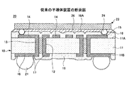
図1及び図2を参照して、従来の半導体装置20について説明する。図1は、従来の半導体装置の断面図であり、図2は、図1に示した基板の断面図である。なお、図2において、図1に示した基板10と同一構成部分には同一の符号を付す。
A
半導体装置20は、大略するとはんだバンプ24を備えた半導体素子23と、基板10とを有しており、基板10の接続パッド15に対して半導体素子23のはんだバンプ24が接続(フリップチップ接続)されると共に、半導体素子23と基板10との間に形成された間隙に、アンダーフィル樹脂26が配設された構成とされている。
The
基板10は、大略すると樹脂基材11と、貫通孔12と、貫通ビア13と、配線14,17と、接続パッド15,18と、ソルダーレジスト16,19と、はんだボール21とを有した構成とされている。基板10は、半導体素子23とマザーボード(図示せず)との間を電気的に接続するためのものである。
The
貫通ビア13は、樹脂基材11を貫通する貫通孔12に配設されており、配線14と接続されている。配線14は、樹脂基材11の面11Aに設けられており、接続パッド15と接続されている。接続パッド15は、例えば、樹脂基材11の面11Aに設けられており、半導体素子23のはんだバンプ24を接続するためのものである。配線14及び接続パッド15は、樹脂基材11の面11Aに銅箔を貼り付け、銅箔上に配線14及び接続パッド15の形状に対応するようレジスト膜をパターニングし、このパターニングされたレジスト膜をマスクとしてエッチングを行うことで形成される(例えば、特許文献1参照。)。
The
ソルダーレジスト16は、樹脂基材11の面11A、及び配線14を覆うと共に、接続パッド15を露出するよう設けられている。配線17は、樹脂基材11の面11Bに設けられており、貫通ビア13と接続されている。接続パッド18は、例えば、樹脂基材11の面11Bに設けられており、配線17と接続されている。接続パッド18は、はんだボール21を配設するためのものである。配線17及び接続パッド18は、樹脂基材11の面11Bに銅箔を貼り付け、銅箔上に配線17及び接続パッド18の形状に対応するようレジスト膜をパターニングし、このパターニングされたレジスト膜をマスクとしてエッチングを行うことで形成される(例えば、特許文献1参照。)。
The
ソルダーレジスト19は、樹脂基材11の面11B、及び配線17を覆うと共に、接続パッド18を露出するよう形成されている。はんだボール21は、接続パッド18に配設されており、はんだボール21はマザーボート(図示せず)と接続される。このような構成とされた基板10の接続パッド15には、半導体素子23のはんだバンプ24が接続される。
The
アンダーフィル樹脂26は、ソルダーレジスト16と半導体素子23との間に配設されている。アンダーフィル樹脂26は、基板10に接続された半導体素子23と樹脂基板11との接続を強固にするためのものである。アンダーフィル樹脂26を設けることにより、基板10と半導体素子23との間の接続信頼性を向上させることができる。
図3は、半導体素子が接続された基板と半導体素子との間の拡大図である。なお、図3において、D1は樹脂基板11上に設けられたソルダーレジスト16と半導体素子23との間の間隙(以下、間隙D1とする)、D2は配線14上に設けられたソルダーレジスト16と半導体素子23との間の間隙(以下、間隙D2とする)、H1ははんだバンプ24の高さ(以下、高さH1とする)をそれぞれ示している。また、図3に示した領域Aは、配線14が設けられた領域を示しており、領域Bは配線14及び接続パッド15が設けられていない領域を示している。
FIG. 3 is an enlarged view between the semiconductor element and the substrate to which the semiconductor element is connected. In FIG. 3, D <b> 1 is a gap between the
しかしながら、半導体素子23が実装される側の樹脂基材11には、配線14が形成された領域Aと、接続パッド15及び配線14が形成されていない領域Bとが存在し、接続パッド15及び配線14は樹脂基材11の面11Aから突出するよう形成されているため、基板10に設けられたソルダーレジスト16の上面16Aは凹凸形状となる。これにより、基板10に接続された半導体素子23と基板10との間隙にアンダーフィル樹脂26を配設した際、配線14上に設けられたソルダーレジスト16と半導体素子23との間の間隙D2は、領域Bに設けられたソルダーレジスト16と半導体素子23との間の間隙D1よりも狭くなってしまい、半導体素子23と基板10との間に均一かつ十分な厚さのアンダーフィル樹脂26を設けることが困難であるという問題があった。
However, the
また、近年の半導体素子の高速化、多機能化及び高集積化による端子の増加や狭ピッチ化に伴い、半導体素子23のはんだバンプ24(外部接続端子)の高さH1は小さくなってきており、配線14上に設けられたソルダーレジスト16と半導体素子23との間の間隙D2は、さらに小さくなる傾向にあり、間隙D2にアンダーフィル樹脂26を設けることが困難であるという問題があった。
In addition, with the recent increase in terminals and narrowing of pitch due to higher speed, multi-functionality and higher integration of semiconductor elements, the height H1 of the solder bumps 24 (external connection terminals) of the
さらに、半導体素子の小型化及び薄膜化に伴い、基板10の厚さが薄くなった場合には、基板10の強度不足により、基板10が変形し、基板10に対して半導体素子23を精度良く接続することが困難であるという問題があった。
Further, when the thickness of the
そこで本発明は、上述した問題点に鑑みなされたものであり、半導体素子と基板との間隙に十分な厚さのアンダーフィル樹脂を均一に配設でき、かつ半導体素子を基板に対して精度良く接続することのできる基板、半導体装置、基板の製造方法、及び半導体装置の製造方法を提供することを目的とする。 Therefore, the present invention has been made in view of the above-described problems, and an underfill resin having a sufficient thickness can be uniformly disposed in the gap between the semiconductor element and the substrate, and the semiconductor element is accurately mounted on the substrate. It is an object of the present invention to provide a substrate that can be connected, a semiconductor device, a method for manufacturing the substrate, and a method for manufacturing the semiconductor device.
上記課題を解決するために本発明では、次に述べる各手段を講じたことを特徴とするものである。 In order to solve the above-mentioned problems, the present invention is characterized by the following measures.
請求項1記載の発明では、基材と、半導体素子に設けられた第1の外部接続端子が接続される配線部とを備えた基板において、前記配線部と一体的に形成され、前記基材を貫通する貫通ビア部を有しており、前記配線部は、該配線部が設けられた側の前記基材の面と面一となるよう構成され、かつ、前記第1の外部接続端子が接続される接続パッドと、該接続パッドと前記貫通ビア部との間を接続する配線とを有しており、前記配線部が設けられた側の前記基材には、前記貫通ビア部及び配線を覆うと共に、前記接続パッドを露出する絶縁層を設けたことを特徴とする基板により、解決できる。 According to the first aspect of the present invention, in a substrate including a base material and a wiring portion to which a first external connection terminal provided in the semiconductor element is connected, the base material is formed integrally with the wiring portion. has a through via extending through the said wiring portion is configured to wiring portion is a surface flush with the substrate side provided, and said first external connection terminal A connection pad to be connected; and a wiring for connecting the connection pad and the through via portion; and the base on the side where the wiring portion is provided includes the through via portion and the wiring. The substrate can be solved by providing an insulating layer that covers the connection pads and exposes the connection pads .
上記発明によれば、半導体素子に設けられた第1の外部接続端子が接続される配線部と、配線部が設けられた側の基材の面とが面一となるよう構成することにより、基板に半導体素子が接続された際、半導体素子と基板との間に形成される間隙を均一にすると共に、十分に確保することができる。また、配線部が設けられた側の基材の面と配線とが面一となるよう構成することにより、配線上に設けられた絶縁層の表面が凸凹することがなくなるため、基板に設けられた絶縁層と半導体素子との間に形成される間隙を均一かつ、十分に確保することができる。 According to the above invention, by configuring the wiring portion to which the first external connection terminal provided in the semiconductor element is connected and the surface of the substrate on the side on which the wiring portion is provided to be flush with each other, When the semiconductor element is connected to the substrate, the gap formed between the semiconductor element and the substrate can be made uniform and sufficiently secured. In addition, since the surface of the base material on the side where the wiring portion is provided and the wiring are flush with each other, the surface of the insulating layer provided on the wiring will not be uneven, so that it is provided on the substrate. The gap formed between the insulating layer and the semiconductor element can be ensured uniformly and sufficiently.
請求項2記載の発明では、前記配線部が設けられた側とは反対側に位置する前記貫通ビア部には、他の基板と接続するための第2の外部接続端子を設けたことを特徴とする請求項1に記載の基板により、解決できる。
The invention according to
上記発明によれば、配線部が設けられた側とは反対側に位置する貫通ビア部に、他の基板と接続するための第2の外部接続端子を設けることにより、従来の基板よりも基板の厚さを薄くして、基板の小型化を図ることができる。 According to the above invention, by providing the second external connection terminal for connecting to another substrate in the through via portion located on the opposite side to the side where the wiring portion is provided, the substrate is more than the conventional substrate. The thickness of the substrate can be reduced to reduce the size of the substrate.
請求項3記載の発明では、第1の外部接続端子を備えた半導体素子と、請求項1または2に記載の基板とを備え、該基板に接続された半導体素子と前記基板との間には、間隙が形成されており、前記間隙には、アンダーフィル材を設けたことを特徴とする半導体装置により、解決できる。
In the third aspect of the present invention, a semiconductor device having a first external connection terminal, and a substrate according to
上記発明によれば、半導体素子と基板との間に形成された間隙に、十分な厚さのアンダーフィル材を均一に配設することができる。これにより、基板と半導体素子との間の接続信頼性を十分に確保することができる。 According to the above invention, the underfill material having a sufficient thickness can be uniformly disposed in the gap formed between the semiconductor element and the substrate. Thereby, the connection reliability between the substrate and the semiconductor element can be sufficiently ensured.
請求項4記載の発明では、基材と、他の基板と接続するための第2の外部接続端子が接続される配線部とを備え、第1の外部接続端子を備えた半導体素子が接続される基板において、前記基材は、前記基材を貫通すると共に、前記配線部と一体的に形成された貫通ビア部を有しており、前記配線部は、該配線部が設けられた側の前記基材の面と面一となるよう構成されており、前記第1の外部接続端子は、前記配線部が設けられた側とは反対側の前記基材に位置する前記貫通ビアと接続され、前記配線部は、他の基板と接続するための第2の外部接続端子が接続される接続パッドと、該接続パッドと前記貫通ビア部との間を接続する配線とを有しており、前記配線部が設けられた側の前記基材には、前記貫通ビア部及び配線を覆うと共に、前記接続パッドを露出する絶縁層を設けたことを特徴とする基板により、解決できる。 In the invention according to claim 4 , the substrate includes a base and a wiring portion to which a second external connection terminal for connection to another substrate is connected, and a semiconductor element including the first external connection terminal is connected. In the substrate, the base material penetrates the base material and has a through via part integrally formed with the wiring part, and the wiring part is provided on the side where the wiring part is provided. The first external connection terminal is connected to the through via located on the base opposite to the side on which the wiring portion is provided. The wiring portion has a connection pad to which a second external connection terminal for connecting to another substrate is connected, and a wiring for connecting the connection pad and the through via portion, The base on the side where the wiring portion is provided covers the through via portion and the wiring, The substrate is characterized by providing an insulating layer to expose the connection pads, can be solved.
上記発明によれば、半導体素子に設けられた第1の外部接続端子は、基材の面と面一とされた貫通ビア部に接続されるため、基板に接続された半導体素子と基板との間に形成される間隙を均一にすると共に、十分に確保することができる。また、配線部が設けられた側の基材の面と配線部とを面一となるよう構成されているので、従来の基板よりも基板の厚さを薄くして、基板の小型化を図ることができる。また、配線部は、配線部が設けられた側の基材の面と面一となるよう構成されているため、絶縁層の表面が凸凹することを防止できる。 According to the above invention, since the first external connection terminal provided in the semiconductor element is connected to the through via portion which is flush with the surface of the base material, the semiconductor element connected to the substrate and the substrate The gap formed between them can be made uniform and sufficiently secured. In addition, since the wiring portion is configured so that the surface of the base material on the side where the wiring portion is provided is flush with the wiring portion, the thickness of the substrate is made thinner than that of the conventional substrate, thereby reducing the size of the substrate. be able to. Moreover, since the wiring portion is configured to be flush with the surface of the substrate on the side where the wiring portion is provided, the surface of the insulating layer can be prevented from being uneven.
請求項5記載の発明では、第1の外部接続端子を備えた半導体素子と、請求項4に記載の基板とを備え、該基板に接続された半導体素子と前記基板との間には、間隙が形成されており、前記間隙には、アンダーフィル材を設けたことを特徴とする半導体装置により、解決できる。 According to a fifth aspect of the present invention, a semiconductor element including the first external connection terminal and the substrate according to the fourth aspect are provided, and a gap is provided between the semiconductor element connected to the substrate and the substrate. This can be solved by a semiconductor device characterized in that an underfill material is provided in the gap.
上記発明によれば、半導体素子と基板との間に形成された間隙に、十分な厚さのアンダーフィル材を均一に配設することができる。これにより、基板と半導体素子との間の接続信頼性を十分に確保することができる。 According to the above invention, the underfill material having a sufficient thickness can be uniformly disposed in the gap formed between the semiconductor element and the substrate. Thereby, the connection reliability between the substrate and the semiconductor element can be sufficiently ensured.
請求項6記載の発明では、基材と、半導体素子に設けられた第1の外部接続端子が接続される配線部と、他の基板と接続するための第2の外部接続端子とを備えた基板の製造方法において、前記基材に溝部と、該溝部と一体的に形成された貫通孔とよりなる開口部を形成する開口部形成工程と、前記開口部の内壁に金属膜を形成する金属膜形成工程と、前記金属膜を給電層として、電解めっき法により前記開口部にめっき膜を析出成長させ、前記貫通孔に前記第2の外部接続端子が接続される貫通ビア部を形成すると共に、前記溝部に前記第1の外部接続端子が接続される配線部を形成するめっき膜形成工程とを含み、前記配線部は、該配線部が設けられた側の前記基材の面と面一となるよう構成され、かつ、前記第1の外部接続端子が接続される接続パッドと、該接続パッドと前記貫通ビア部との間を接続する配線とを有しており、前記貫通ビア部及び配線を覆うと共に、前記接続パッドを露出する絶縁層を前記基材に形成する絶縁層形成工程とを設けたことを特徴とする基板の製造方法により、解決できる。 The invention according to claim 6 includes a base material, a wiring portion to which the first external connection terminal provided in the semiconductor element is connected, and a second external connection terminal for connection to another substrate. In the method for manufacturing a substrate, an opening forming step for forming an opening made of a groove and a through hole formed integrally with the groove in the base material, and a metal for forming a metal film on the inner wall of the opening A film forming step, and using the metal film as a power supply layer, depositing and growing a plating film on the opening by electrolytic plating, and forming a through via portion to which the second external connection terminal is connected to the through hole the saw including a plating film forming step of the first external connection terminal to form a wiring portion connected to the groove, the wiring part, the surface and the surface of the substrate on the side where the wiring portion is provided And the first external connection terminal is connected. A connection pad, and a wiring connecting the connection pad and the through via part, and covering the through via part and the wiring and an insulating layer exposing the connection pad on the base material This can be solved by a method for manufacturing a substrate, characterized in that an insulating layer forming step is provided .
上記発明によれば、基材に溝部と、溝部と一体的に形成された貫通孔とよりなる開口部を形成し、開口部の内壁に金属膜を形成して、電解めっき法により開口部にめっき膜を析出成長させることにより、半導体素子に設けられた第1の外部接続端子が接続される配線部と貫通ビア部とが、配線部が設けられた側の基材の面と面一になるよう加工することができる。また、配線は、配線部が設けられた側の基材の面と面一となるよう形成されるため、貫通ビア部及び配線を覆う絶縁層の表面が凸凹することがなくなり、基板に接続された半導体素子と絶縁層との間に形成される間隙を均一かつ、十分に確保することができる。 According to the above invention, the opening comprising the groove and the through hole formed integrally with the groove is formed in the base material, the metal film is formed on the inner wall of the opening, and the opening is formed by electrolytic plating. By depositing and growing the plating film, the wiring portion to which the first external connection terminal provided in the semiconductor element is connected and the through via portion are flush with the surface of the substrate on the side where the wiring portion is provided. Can be processed. Also, since the wiring is formed so as to be flush with the surface of the base material on the side where the wiring portion is provided, the surface of the insulating layer covering the through via portion and the wiring is not uneven, and is connected to the substrate. The gap formed between the semiconductor element and the insulating layer can be ensured uniformly and sufficiently.
請求項7記載の発明では、前記めっき膜形成工程において、前記めっき膜が前記基材の面よりも突出した際には、前記めっき膜と前記基材の面が面一となるように前記突出しためっき膜を研磨するめっき膜研磨工程を設けたことを特徴とする請求項6に記載の基板の製造方法により、解決できる。 In the invention of claim 7 , in the plating film forming step, when the plating film protrudes from the surface of the base material, the protrusion protrudes so that the surface of the plating film and the base material are flush with each other. It can solve by the manufacturing method of the board | substrate of Claim 6 provided with the plating film grinding | polishing process which grind | polishes the plated film which carried out.
上記発明によれば、めっき膜形成工程において、めっき膜が基材の面よりも突出した際、めっき膜と基材の面とが面一となるよう研磨することにより、配線部及び貫通ビア部と配線部が設けられた側の基材の面とを面一にすることができる。 According to the above invention, in the plating film forming step, when the plating film protrudes from the surface of the substrate, polishing is performed so that the plating film and the surface of the substrate are flush with each other. And the surface of the base material on the side where the wiring portion is provided can be flush with each other.
請求項8記載の発明では、基材と、配線部とを有した基板と、前記配線部に接続される第1の外部接続端子を備えた半導体素子とを備え、前記基板に接続された半導体素子と前記基板との間に形成される間隙に、アンダーフィル材を設けた半導体装置の製造方法において、前記基材を支持する支持部材に、前記基材を配設する基材配設工程と、該基材配設工程後に、請求項6または7に記載の基板の製造方法により前記基板を製造する基板製造工程と、該基板製造工程後に、前記第1の外部接続端子を前記配線部に接続する半導体素子接続工程と、該半導体素子接続工程後に、前記基板に接続された半導体素子と前記基板との間に形成された間隙に、前記アンダーフィル材を配設するアンダーフィル材配設工程と、該アンダーフィル樹脂配設工程後に、前記支持部材を除去する支持部材除去工程とを含んだことを特徴とする半導体装置の製造方法により、解決できる。 According to an eighth aspect of the present invention, there is provided a semiconductor comprising a substrate having a base material, a wiring portion, and a semiconductor element having a first external connection terminal connected to the wiring portion, the semiconductor element being connected to the substrate In a method for manufacturing a semiconductor device in which an underfill material is provided in a gap formed between an element and the substrate, a base material disposing step of disposing the base material on a support member that supports the base material; A substrate manufacturing step for manufacturing the substrate by the substrate manufacturing method according to claim 6 or 7 after the base material disposing step, and after the substrate manufacturing step, the first external connection terminal is connected to the wiring portion. A semiconductor element connecting step for connecting, and an underfill material disposing step for disposing the underfill material in a gap formed between the semiconductor element connected to the substrate and the substrate after the semiconductor element connecting step. And underfill resin arrangement After the degree, by the method of manufacturing a semiconductor device characterized by including a support member removing step of removing the supporting member, it can be solved.
上記発明によれば、基材を支持する支持部材上に基材を配設して、請求項6または7に記載の基板の製造方法により基板を製造することにより、基材の厚さが薄い場合でも、精度良く基板の製造を行うことができる。また、基材を支持部材により支持した状態で、基板に半導体素子を接続することで、基材の厚さが薄い場合でも、基板と半導体素子とを確実に接続することができる。 According to the invention, by arranging the substrate on a support member for supporting the substrate, by manufacturing a substrate by the method for producing a substrate according to claim 6 or 7, a thin thickness of the base material Even in this case, the substrate can be manufactured with high accuracy. Further, by connecting the semiconductor element to the substrate while the base material is supported by the support member, the substrate and the semiconductor element can be reliably connected even when the thickness of the base material is thin.
請求項9記載の発明では、基材と、他の基板と接続するための第2の外部接続端子が接続される配線部とを備え、第1の外部接続端子を備えた半導体素子が接続される基板の製造方法において、前記基材に溝部と、該溝部と一体的に形成された貫通孔とよりなる開口部を形成する開口部形成工程と、前記開口部の内壁に金属膜を形成する金属膜形成工程と、前記金属膜を給電層として、電解めっき法により前記開口部にめっき膜を析出成長させ、前記貫通孔に前記第1の外部接続端子と接続される貫通ビア部を形成すると共に、前記溝部に前記第2の外部接続端子が接続される配線部を形成するめっき膜形成工程とを含み、前記配線部は、該配線部が設けられた側の前記基材の面と面一となるよう構成され、かつ、前記第2の外部接続端子が接続される接続パッドと、該接続パッドと前記貫通ビア部との間を接続する配線とを有しており、前記貫通ビア部及び配線を覆うと共に、前記接続パッドを露出する絶縁層を前記基材に形成する絶縁層形成工程とを設けたことを特徴とする基板の製造方法により、解決できる。 The invention according to claim 9 includes a base material and a wiring portion to which a second external connection terminal for connection to another substrate is connected, and a semiconductor element including the first external connection terminal is connected. In the substrate manufacturing method, an opening forming step of forming an opening made of a groove and a through-hole formed integrally with the groove on the base material, and forming a metal film on the inner wall of the opening A metal film forming step, and using the metal film as a power feeding layer, a plating film is deposited and grown in the opening by electrolytic plating, and a through via portion connected to the first external connection terminal is formed in the through hole. together, look including a plating film forming step of forming a wiring portion to which the second external connection terminal is connected to the groove portion, the wiring portion includes a surface of the substrate on the side where the wiring portion is provided And the second external connection terminal is configured to be flush with each other. A connection pad that is connected, and a wiring that connects between the connection pad and the through-via portion. The insulating layer that covers the through-via portion and the wiring and exposes the connection pad is formed on the base. This can be solved by a method for manufacturing a substrate, characterized in that an insulating layer forming step for forming a material is provided .
上記発明によれば、半導体素子と接続される貫通ビア部は、基材の面と面一となるよう形成することにより、基板に接続される半導体素子と基板との間に形成される間隙を均一、かつ十分に確保することができる。また、第2の外部接続端子が接続される配線部は、配線部が設けられた側の基材の面と面一となるよう形成されるため、基材、貫通ビア部及び配線に設けられた絶縁層の表面が凸凹することを防止できる。 According to the above invention, the through via portion connected to the semiconductor element is formed so as to be flush with the surface of the base material, thereby forming a gap formed between the semiconductor element connected to the substrate and the substrate. Uniform and sufficient. In addition, since the wiring portion to which the second external connection terminal is connected is formed so as to be flush with the surface of the base material on the side where the wiring portion is provided, the wiring portion is provided on the base material, the through via portion, and the wiring. It is possible to prevent the surface of the insulating layer from being uneven.
請求項10記載の発明では、前記めっき膜形成工程において、前記めっき膜が前記基材の面よりも突出した際には、前記めっき膜と前記基材の面が面一となるように前記突出しためっき膜を研磨するめっき膜研磨工程を設けたことを特徴とする請求項9に記載の基板の製造方法により、解決できる。
In the invention of
上記発明によれば、めっき膜形成工程において、めっき膜が基材の面よりも突出した際、めっき膜と基材の面が面一となるように研磨することにより、配線部及び貫通ビア部と配線部が設けられた側の基材の面とを面一にすることができる。これにより、基材から突出する配線部を有した従来の基板よりも基板の厚さを薄くして、基板の小型化を図ることができる。 According to the above invention, in the plating film forming step, when the plating film protrudes from the surface of the base material, polishing is performed so that the surface of the plating film and the base material is flush with each other. And the surface of the base material on the side where the wiring portion is provided can be flush with each other. Thereby, the board | substrate thickness can be made thinner than the conventional board | substrate which has the wiring part which protrudes from a base material, and size reduction of a board | substrate can be achieved.
本発明によれば、表面の平坦性が高く、半導体素子と基板との間隙に十分な厚さのアンダーフィル材を均一に配設することができ、かつ半導体素子を基板に対して精度良く接続することのできる基板、半導体装置、基板の製造方法、及び半導体装置の製造方法を提供できる。 According to the present invention, the surface flatness is high, an underfill material having a sufficient thickness can be uniformly disposed in the gap between the semiconductor element and the substrate, and the semiconductor element is accurately connected to the substrate. A substrate, a semiconductor device, a method for manufacturing a substrate, and a method for manufacturing a semiconductor device can be provided.
次に、図面に基づいて本発明の実施例を説明する。
(第1実施例)
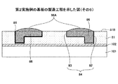
始めに、図4を参照して、本発明の第1実施例の半導体装置60について説明する。図4は、本発明の第1実施例の半導体装置を示した図である。半導体装置60は、大略すると基板40と、半導体素子63とを有している。半導体装置60は、半導体素子63が基板40に対してフリップチップ接続されると共に、半導体素子本体64と基板40との間隙67にアンダーフィル樹脂66を配設した構成とされている。アンダーフィル樹脂66は、基板40に接続されたはんだバンプ65を保護して、基板40と半導体素子63との間の接続信頼性を向上させるためのものである。半導体素子63は、半導体素子本体64に第1の外部接続端子であるはんだバンプ65が設けられた構成とされている。はんだバンプ65は、拡散防止膜56を介して、基板40の接続パッド49に接続されている。
Next, embodiments of the present invention will be described with reference to the drawings.
(First embodiment)
First, the
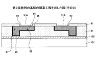
次に、図5乃至図7を参照して、本実施例の基板40について説明する。図5は、第1実施例の基板の断面図(図6に示した基板40のE−E線方向の断面図)であり、図6は、図5に示した基板をC視した図(平面図)であり、図7は、図5に示した基板をD視した図である。
Next, the
基板40は、大略すると基材41と、貫通ビア部47と、配線部48と、拡散防止膜52,56と、ソルダーレジスト57とを有した構成とされている。基材41には、貫通ビア部47及び配線部48を配設するための開口部74が形成されている。開口部74は、貫通ビア部47が配設される貫通孔75と、配線部49が配設される溝部76とを有した構成とされている。基材41には、例えば、樹脂基材を用いることができる。なお、以下の説明においては、基材41として樹脂基材を用いた場合について説明する。
The
貫通ビア部47は、基材41を貫通するよう貫通孔75に配設されており、溝部76に配設された配線部48と一体的に形成されている。貫通ビア部47は、はんだボール54を接続するためのものであり、配線部48の接続パッド49には、半導体素子63のはんだバンプ65が接続される。貫通ビア部47及び配線部48は、金属膜45と、Cuめっき膜46とにより構成されている。金属膜45は、電解めっき法によりCuめっき膜46を形成する際の給電層である。金属膜45には、例えば、無電解めっき法により形成されたNi膜、Cu膜を用いることができる。
The through via
基材41の面41B側に位置する貫通ビア部47の端部には、拡散防止膜52が設けられている。拡散防止膜52は、はんだのぬれ性向上や、貫通ビア部47に含まれるCuがはんだボール54に拡散することを防止するためのものである。拡散防止膜52には、例えば、Ni層/Au層の積層膜を用いることができる。第2の外部接続端子であるはんだボール54は、基板40に半導体素子63を搭載し、アンダーフィル樹脂66を充填した後に、拡散防止膜52上に配設される。はんだボール54は、他の基板、例えば、マザーボードと基板40との間を電気的に接続するためのものである。
A
配線部48は、基材41の面41A側に設けられており、接続パッド49と配線51とを有した構成とされている(図6参照)。接続パッド49は、半導体素子63のはんだバンプ65が接続されるものであり、配線51は、接続パッド49と貫通ビア部47との間を電気的に接続するためのものである。配線部48である接続パッド49及び配線51は、基材41の面41Aと面一となるよう構成されている。絶縁層であるソルダーレジスト57は、基材41の面41A側に貫通ビア部47及び配線51を覆うと共に、接続パッド49を露出するよう形成されている。
The
このように、配線部48を基材41の面41Aと面一となるよう構成することにより、はんだバンプ65を接続パッド49に接続した際、基板40に設けられたソルダーレジスト57と半導体素子本体64との間に形成される間隙67を均一にすると共に、十分に確保することができる。これにより、間隙67に十分な厚さのアンダーフィル樹脂66を均一に配設して、半導体素子63と基板40の間の接続信頼性を十分に確保することができる。
In this way, by configuring the
ソルダーレジスト57から露出された接続パッド49には、拡散防止膜56が設けられている。拡散防止膜56は、はんだのぬれ性向上や、接続パッド49に含まれるCuがはんだバンプ65に拡散することを防止するためのものである。拡散防止膜56には、例えば、Ni層/Au層の積層膜を用いることができる。
A
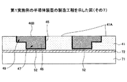
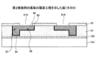
次に、図8乃至図21を参照して、第1実施例の半導体装置60の製造方法について説明する。図8乃至図20は、第1実施例の半導体装置の製造工程を示した図であり、図21は、図11に示した構造体にCuめっき膜を析出成長させた図である。なお、図8乃至図20において、図4に示した半導体装置60と同一構成部分には同一の符号を付す。
A method for manufacturing the
始めに、図8に示すように、支持部材71上に金属層72を設け、金属層72を介して支持部材71に基材41を配設する(基材配設工程)。支持部材71は、基材41の厚さM1が薄い場合に発生する反りや撓みを抑制するためのものである。支持部材71には、例えば、エポキシやポリイミド等の樹脂板や、アルミ、銅等の金属板を用いることができる。なお、支持部材71に金属板を用いる場合には、金属層72を設ける必要がなく、金属層72を形成する工程を省略することができる。
First, as shown in FIG. 8, the
このように、支持部材71上に基材41を配設して、基板40の製造を行うことにより、基材41の厚さM1が薄い場合でも、基板40を精度良く製造することができる。金属層72は、電解めっき法により拡散防止膜52を形成する際の給電層である。金属層72は、例えば、無電解めっき法やスパッタ法により形成することができる。金属層72の材料には、例えば、Cu,Ni,Al等を用いることができる。なお、金属層72が設けられた支持部材71上に、樹脂を塗布して、基材41を形成しても良い。
In this way, by arranging the
次に、図9に示すように、基材41に、溝部76と、溝部76と一体的に形成された貫通孔75よりなる開口部74を形成する(開口部形成工程)。この際、金属層72は、貫通孔75により露出される。開口部74は、例えば、ドリルを用いたドリル加工、レーザ加工、微細な金型を用いた金型加工のいずれかの方法により形成することができる。金型加工を用いる場合には、金属層72が形成された支持部材71上に、樹脂(図9に示した基材41に相当する)を塗布又は樹脂フィルム(図9に示した基材41に相当する)を貼着し、次に、樹脂(又は樹脂フィルム)を半硬化させ、開口部74を形成するための凸部を有した金型を半硬化状態の樹脂(又は樹脂フィルム)に押し付けて、凸部の形状を転写し、樹脂(又は樹脂フィルム)を加熱して硬化させることで、基材41に開口部74が形成される。
Next, as shown in FIG. 9, an
続いて、図10に示すように、金属層72を給電層として、電解めっき法により貫通孔75の底部に拡散防止膜52を形成する。なお、拡散防止膜52に替えて、はんだボール54の接合に都合が良いようなはんだ膜(はんだめっき法により形成される)を用いても良い。次に、図11に示すように、図10に示した構造体上に金属膜45を形成する。金属膜45は、開口部74にCuめっき膜46を析出成長させるための給電層である。金属膜45は、例えば、無電解めっき法やスパッタ法により形成することができる。金属膜45には、例えば、銅やニッケルを用いることができる。
Subsequently, as illustrated in FIG. 10, the
次に、図12に示すように、基材41の面41A上に形成された金属膜45を研磨により除去して、開口部74の内壁にのみ金属膜45を残す(金属膜形成工程)。続いて、図13に示すように、金属膜45を給電層として、電解めっき法により開口部74にCuめっき膜46を析出成長させる(めっき膜形成工程)。なお、図13において、Cuめっき膜46Aは、基材41の面41Aから突出した部分のCuめっき膜を示している。
Next, as shown in FIG. 12, the
次に、図14に示すように、基材41の面41Aから突出したCuめっき膜46Aの研磨を行って、Cuめっき膜46の面46Bと基材41の面41Aとを面一にする(めっき膜研磨工程)。これにより、溝部76に形成された配線部48(接続パッド49及び配線51)、及び貫通孔75に形成された貫通ビア部47を基材41の面41Aと面一にすることができる。
Next, as shown in FIG. 14, the
このように、配線部48が基材41の面41Aと面一になるよう形成することにより、基材41の面41Aから接続パッド49及び配線51が突出することがなくなり、半導体素子63を基板40に接続させた際、半導体素子本体64と基板40との間隙67を均一にすると共に、十分に確保することができる。なお、めっき膜形成工程において、Cuめっき膜46Aの突出量が少ない場合には、めっき膜研磨工程を省略しても良い。
Thus, by forming the
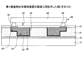
次に、図15に示すように、配線51及び貫通ビア部47を覆うと共に、接続パッド49を露出する開口部57Aを有したソルダーレジスト57を形成する(絶縁層形成工程)。続いて、図16に示すように、めっき法により開口部57Aに露出された接続パッド49上にNi層/Au層からなる拡散防止膜56を形成する。なお、拡散防止膜56に替えて、半導体素子63の接合に都合が良いようなはんだ膜(はんだめっき法により形成される)を用いても良い。
Next, as shown in FIG. 15, a solder resist 57 that covers the
次に、図17に示すように、基材41を支持部材71に支持した状態で、拡散防止膜56を介して、半導体素子63のはんだバンプ65を接続パッド49にフリップチップ接続する(半導体素子接続工程)。
Next, as shown in FIG. 17, the
このように、支持部材71により基材41を支持した状態で、半導体素子63を接続パッド49に接続することで、基材41の厚さM1が薄い場合でも、基材41が撓むことが防止でき、半導体素子63のはんだバンプ65を接続パッド49に対して精度良く接続することができる。
Thus, by connecting the
次に、図18に示すように、半導体素子本体64とソルダーレジスト57との間に形成された間隙67に、アンダーフィル樹脂66を配設する(アンダーフィル材配設工程)。これにより、間隙67に十分な厚さのアンダーフィル樹脂66を均一に配設して、基板40と半導体素子63との間の接続信頼性を十分に確保することができる。
Next, as shown in FIG. 18, an
次に、図19に示すように、支持部材71及び金属層72の除去処理を行う(支持部材除去工程)。ここで、支持部材71及び金属層72の除去処理について説明する。支持部材71に樹脂板を用いた場合には、支持部材71を剥離後に、金属層72をウエットエッチングにより除去する。また、支持部材71がポリイミド(樹脂)からなり、この表面に無電解銅めっき法で金属層72が形成された場合には、容易に金属層72から支持部材71を剥離させることができる。金属層72に銅を用いた場合には、銅をウエットエッチングする際に使用されるエッチング液に拡散防止膜52が溶解されにくいため、金属層72のみ容易に除去することができる。支持部材71に金属板を用いた場合には、ウエットエッチングにより除去することができる。また、支持部材71である金属板を研磨により除去後、ウエットエッチングにより金属層72の除去を行っても良い。
Next, as shown in FIG. 19, the removal process of the
続いて、図20に示すように、拡散防止膜52を介して、はんだボール54を貫通ビア部47に接続する。これにより、基板40に半導体素子63が接続された半導体装置60が製造される。
Subsequently, as shown in FIG. 20, the
以上説明したように、配線部48及び貫通ビア部47が基材41の面41Aと面一となるよう形成することにより、半導体素子本体64と基板40との間に形成される間隙67を均一にすると共に、十分に確保して、間隙67に十分な厚さのアンダーフィル樹脂66を配設することができる。これにより、基板40と半導体素子63との接続を強固にすることにより、基板40及び/又は半導体素子63が破損することを防止できる。また、基材41の厚さM1が薄い場合において、基板40を精度良く加工すると共に、半導体素子63のはんだバンプ65を接続パッド49に対して精度良く接続することができる。
As described above, by forming the
なお、図21に示すように、図11に示した構造体にCuめっき膜46を形成し、続いて、研磨により図14に示した構造体の形状に加工し、その後、図15乃至図20に示した製造工程により半導体装置60を製造しても良い。
(第2実施例)
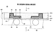
始めに、図22を参照して、本発明の第2実施例の半導体装置100について説明する。図22は、本発明の第2実施例の半導体装置を示した図である。半導体装置100は、大略すると基板80と、半導体素子63とを有している。半導体装置100は、半導体素子63が基板80に対してフリップチップ接続され、半導体素子本体64と基板80との間隙110には、アンダーフィル樹脂98が配設されている。
As shown in FIG. 21, a
(Second embodiment)
First, the
半導体素子63は、半導体素子本体64と、第1の外部接続端子であるはんだバンプ65とを有した構成とされている。はんだバンプ65は、拡散防止膜95を介して、基材81の面81A側に位置する貫通ビア部87の端部と接続されている。
The
次に、図23乃至図25を参照して、本実施例の基板80について説明する。図23は、第2実施例の基板の断面図(図25に示した基板80のF−F線方向の断面図)であり、図24は、図23に示した基板をC視した図(平面図)であり、図25は、図23に示した基板をD視した図である。
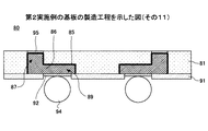
Next, the
基板80は、大略すると基材81と、貫通ビア部87と、配線部88と、拡散防止膜92,95と、はんだボール94と、ソルダーレジスト91とを有した構成とされている。基材81には、貫通ビア部87及び配線部88を配設するための開口部84が形成されている。開口部84は、貫通ビア部87が配設される貫通孔82と、配線部88が配設される溝部83とを有した構成とされている。基材81には、例えば、樹脂基材を用いることができる。なお、以下の説明においては、基材81として樹脂基材を用いた場合について説明する。
The
貫通ビア部87は、基材81を貫通するよう貫通孔82に配設されており、溝部83に配設された配線部88と一体的に形成されている。配線部88が形成されていない側の貫通ビア部87には、半導体素子63のはんだバンプ65が接続される。
The through via
このように、半導体素子63のはんだバンプ65を配線部88が形成されていない側の貫通ビア部87に接続することにより、半導体素子63と基板80との間に形成される間隙110を均一、かつ十分に確保することができる。これにより、間隙110に十分な厚さのアンダーフィル樹脂98を均一に配設して、半導体素子63と基板80との間の接続信頼性を向上させることができる。
Thus, by connecting the
貫通ビア部87及び配線部88は、金属膜85と、Cuめっき膜86とにより構成されている。金属膜85は、電解めっき法によりCuめっき膜86を形成する際の給電層である。金属膜85には、例えば、無電解めっき法により形成されたNi膜、Cu膜を用いることができる。
The through via
配線部88は、接続パッド89と、配線90とを有した構成とされている。配線部88は、基材81の面81B側に貫通ビア部87と一体的に形成されている。接続パッド89は、第2の外部接続端子であるはんだボール94を接続するためのものである。配線90は、接続パッド89と貫通ビア部87との間を電気的に接続するためのものである。配線部88及び貫通ビア部87は、基材81の面81Bと面一となるように形成されている。
The
このように、配線部88を基材81の面81Bと面一となるよう構成することにより、接続パッド89及び配線90が基材81の面81Bから突出することがなくなるため、従来の基板10よりも基板80の厚さM2を薄くして、基板80の小型化を図ることができる。
Thus, by configuring the
絶縁層であるソルダーレジスト91は、貫通ビア部87及び配線90を覆うと共に、接続パッド89を露出するよう基材81に形成されている。ソルダーレジスト91は、はんだボール94が接続される際のはんだショートを抑制すると共に、貫通ビア部87及び配線90を保護するためのものである。拡散防止膜92は、ソルダーレジスト91に露出された接続パッド89上に設けられている。拡散防止膜92は、はんだのぬれ性向上や、はんだボール94に接続パッド89に含まれるCuが拡散することを防止するためのものである。拡散防止膜92には、例えば、Ni層/Au層の積層膜を用いることができる。第2の外部接続端子であるはんだボール94は、拡散防止膜92を介して、接続パッド89に接続されている。はんだボール94は、他の基板、例えば、マザーボードと基板80との間を電気的に接続するためのものである。
A solder resist 91, which is an insulating layer, is formed on the
基材81を貫通する貫通ビア部87は、配線部88と一体的に設けられている。基材81の面81A側に位置する貫通ビア部87の端部には、基材81の面81Aと面一となるよう拡散防止膜95が設けられている。拡散防止膜95が設けられた貫通ビア部87には、半導体素子63のはんだバンプ65が電気的に接続される。拡散防止膜95は、はんだのぬれ性向上や、はんだバンプ65に貫通ビア部87に含まれるCuが拡散することを防止するためのものである。拡散防止膜95には、例えば、Ni層/Au層の積層膜を用いることができる。
A through via
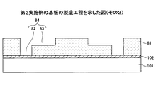
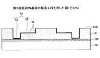
次に、図26乃至図36を参照して、第2実施例の基板80の製造方法について説明する。図26乃至図36は、第2実施例の基板の製造工程を示した図であり、図37は、図36に示した基板に半導体素子を接続させた半導体装置の断面図である。また、図38は、図29に示した構造体にCuめっき膜を析出成長させた図である。
Next, a method for manufacturing the
始めに、図26に示すように、支持部材101上に金属層102を設け、金属層102を介して支持部材101上に基材81を配設する(基材配設工程)。支持部材101は、基材81の厚さM3が薄い場合に発生する反りや撓みを抑制するためのものである。支持部材101には、例えば、エポキシやポリイミド等の樹脂板や、アルミ、銅等の金属板を用いることができる。なお、支持部材101に金属板を用いる場合には、金属層102を設ける必要がなく、金属層102を形成する工程を省略することができる。
First, as shown in FIG. 26, a
このように、支持部材101上に基材81を配設して、基板80の製造を行うことにより、基材81の厚さM3が薄い場合でも、精度良く基板80を製造することができる。金属層102は、電解めっき法により拡散防止膜95を形成する際の給電層である。金属層102は、例えば、無電解めっき法やスパッタ法により形成することができる。金属層102の材料には、例えば、Cu,Ni,Al等を用いることができる。なお、金属層102が設けられた支持部材101上に、樹脂を塗布して、基材81を形成しても良い。
In this way, by arranging the
次に、図27に示すように、基材81に開口部84を形成する(開口部形成工程)。開口部84は、溝部83と、溝部83と一体的に形成された貫通孔82とから構成されている。この際、金属層102は、貫通孔82により露出される。開口部84は、例えば、ドリルを用いたドリル加工、レーザ加工、微細な金型を用いた金型加工のいずれかの方法により形成することができる。金型加工を用いる場合には、金属層102が形成された支持部材101上に、樹脂(図27に示した基材81に相当する)を塗布又は樹脂フィルム(図27に示した基材81に相当する)を貼着し、次に、樹脂(又は樹脂フィルム)を半硬化させ、開口部84を形成するための凸部を有した金型を半硬化状態の樹脂(又は樹脂フィルム)に押し付けて、凸部の形状を転写し、樹脂(又は樹脂フィルム)を加熱して硬化させることで、基材81に開口部84が形成される。
Next, as shown in FIG. 27, an
続いて、図28に示すように、金属層102を給電層として、電解めっき法により貫通孔82の底部に、基材81の面81Aと面一となる拡散防止膜95を形成する。なお、拡散防止膜95に替えて、半導体素子63の接合に都合が良いようなはんだ膜(はんだめっき法により形成される)を用いても良い。
Subsequently, as shown in FIG. 28, a
このように、半導体素子63のはんだバンプ65が接続される拡散防止膜95を、基材81の面81Aと面一となるよう形成することにより、半導体素子63が基板80に接続された際、半導体素子本体64と基板80との間に形成される間隙110を均一、かつ十分に確保することができる。
Thus, the
次に、図29に示すように、図28に示した構造体上に金属膜85を形成する。金属膜85は、開口部84にCuめっき膜86を析出成長させる際の給電層である。金属膜85は、例えば、無電解めっき法やスパッタ法により形成することができる。金属膜85には、例えば、銅やニッケルを用いることができる。
Next, as shown in FIG. 29, a
次に、図30に示すように、基材81の面81Bに形成された金属膜85を研磨により除去して、開口部84の内壁にのみ金属膜85を残す(金属膜形成工程)。続いて、図31に示すように、金属膜85を給電層として、電解めっき法により開口部84に形成された金属膜85上にCuめっき膜86を析出成長させる(めっき膜形成工程)。なお、図31において、Cuめっき膜86Aは、基材81の面81Bから突出したCuめっき膜を示している。
Next, as shown in FIG. 30, the
次に、図32に示すように、基材81の面81Bから突出したCuめっき膜86Aの研磨を行って、研磨後のCuめっき膜86の面86Bと基材81の面81Bとを面一にする(めっき膜研磨工程)。これにより、溝部83に形成された配線部88(図示せず)、及び貫通孔82に形成された貫通ビア部87を基材81の面81Bと面一にすることができる。
Next, as shown in FIG. 32, the
このように、配線部88を基材81の面81Bと面一となるように形成することにより、従来の基板10よりも基板80の厚さM2を薄くして、基板80の小型化を図ることができる。なお、めっき膜形成工程において、Cuめっき膜86Aの突出量(基材81の面81Bからの突出量)が少ない場合には、めっき膜研磨工程を省略しても良い。
Thus, by forming the
次に、図33に示すように、貫通ビア部87及び配線90を覆うと共に、接続パッド89を露出する開口部91Aを有したソルダーレジスト91を図32に示した構造体上に形成する(絶縁層形成工程)。続いて、図34に示すように、めっき法により接続パッド89上に拡散防止膜92を形成する。なお、拡散防止膜92に替えて、はんだボール94の接合に都合が良いようなはんだ膜(はんだめっき法により形成される)を用いても良い。
Next, as shown in FIG. 33, a solder resist 91 is formed on the structure shown in FIG. 32 so as to cover the through via
次に、図35に示すように、拡散防止膜92にはんだボール94を配設する。これにより、基板80が製造される。その後、図36に示すように、支持部材101及び金属層102の除去処理を行う。ここで、支持部材101及び金属層102の除去処理について説明する。支持部材101に樹脂板を用いた場合には、支持部材101を剥離後に、金属層102をウエットエッチングにより除去する。また、支持部材101がポリイミド(樹脂)からなり、この表面に無電解銅めっき法で金属層102が形成された場合には、容易に金属層102から支持部材101を剥離させることができる。金属層102に銅を用いた場合には、銅をウエットエッチングする際に使用されるエッチング液に拡散防止膜95が溶解されにくいため、金属層102のみ容易に除去することができる。支持部材101に金属板を用いた場合には、ウエットエッチングにより除去することができる。また、支持部材101である金属板を研磨により除去後、ウエットエッチングにより金属層102の除去を行っても良い。
Next, as shown in FIG. 35,
続いて、図37に示すように、半導体素子63のはんだバンプ65を、拡散防止膜95を介して接続パッド87にフリップチップ接続し、半導体素子本体64と基板80との間隙110にアンダーフィル樹脂98を配設することで、半導体装置100が製造される。
Subsequently, as shown in FIG. 37, the
以上説明したような製造方法で基板80を製造することにより、半導体素子本体64と基板80との間の間隙110に均一、かつ十分な厚さのアンダーフィル樹脂98を配設することにより、基板80と半導体素子63との間の接続信頼性を十分に確保することができる。また、基材81の厚さM3が薄い場合においても、基板80を精度良く製造することができる。さらに、配線部88を基材81の面81Bと面一となるように形成して、基板80の厚さM2を薄くすることにより、基板80の小型化を図ることができる。
By manufacturing the
なお、めっき膜形成工程において、Cuめっき膜86Aの突出量(基材81の面81Bからの突出量)が少ない場合には、めっき膜研磨工程を省略しても良い。また、図38に示すように、図29に示した構造体にCuめっき膜86を形成し、続いて、研磨により図32に示した構造体の形状に加工し、その後、図33乃至図36に示した製造工程により基板80を製造しても良い。
In the plating film forming step, when the protruding amount of the
以上、本発明の好ましい実施例について詳述したが、本発明はかかる特定の実施形態に限定されるものではなく、特許請求の範囲内に記載された本発明の要旨の範囲内において、種々の変形・変更が可能である。なお、第1及び第2実施例の基板40,80において、基材41,81は樹脂基材に限定されない。
The preferred embodiments of the present invention have been described in detail above, but the present invention is not limited to such specific embodiments, and various modifications can be made within the scope of the gist of the present invention described in the claims. Deformation / change is possible. In the
本発明によれば、半導体素子と基板との間隙に十分な厚さのアンダーフィル樹脂を均一に配設することができ、かつ半導体素子を基板に対して精度良く接続することのできる基板、半導体装置、基板の製造方法、及び半導体装置の製造方法に適用できる。 ADVANTAGE OF THE INVENTION According to this invention, the underfill resin of sufficient thickness can be uniformly arrange | positioned in the clearance gap between a semiconductor element and a board | substrate, and the board | substrate which can connect a semiconductor element with a board | substrate with sufficient precision, a semiconductor The present invention can be applied to a device, a substrate manufacturing method, and a semiconductor device manufacturing method.
10,40,80 基板
11 樹脂基材
11A,11B,41A,41B,46B,81A,81B,86B 面
12,75,82 貫通孔
13 貫通ビア
14,17,51,90 配線
15,18,49,89 接続パッド
16,19,57,91 ソルダーレジスト
16A 上面
20,60,100 半導体装置
21,54,94 はんだボール
23,63 半導体素子
24,65 はんだバンプ
26,66,98 アンダーフィル樹脂
41,81 基材
45,85 金属膜
46,46A,86,86A Cuめっき膜
47,87 貫通ビア部
48,88 配線部
52,56,92,95 拡散防止膜
57A,74,84,91A 開口部
63 半導体素子
64 半導体素子本体
67,110 間隙
71,101 支持部材
72,102 金属層
76,83 溝部
A,B 領域
D1,D2 間隙
H1 高さ
M1〜M3 厚さ
10, 40, 80
Claims (10)
前記配線部と一体的に形成され、前記基材を貫通する貫通ビア部を有しており、
前記配線部は、該配線部が設けられた側の前記基材の面と面一となるよう構成され、かつ、前記第1の外部接続端子が接続される接続パッドと、該接続パッドと前記貫通ビア部との間を接続する配線とを有しており、
前記配線部が設けられた側の前記基材には、前記貫通ビア部及び配線を覆うと共に、前記接続パッドを露出する絶縁層を設けたことを特徴とする基板。 In a substrate including a base material and a wiring portion to which a first external connection terminal provided in the semiconductor element is connected,
It is formed integrally with the wiring part, and has a through via part that penetrates the base material,
The wiring portion is configured to be flush with the surface of the base on the side where the wiring portion is provided , and the connection pad to which the first external connection terminal is connected, the connection pad and the And wiring that connects between the through vias,
Board the wiring portion on the said substrate side provided, covering the through via portion and the wiring, characterized in that an insulating layer for exposing the connection pads.
該基板に接続された半導体素子と前記基板との間には、間隙が形成されており、
前記間隙には、アンダーフィル材を設けたことを特徴とする半導体装置。 A semiconductor element provided with a first external connection terminal, and the substrate according to claim 1 or 2 ,
A gap is formed between the semiconductor element connected to the substrate and the substrate,
A semiconductor device, wherein an underfill material is provided in the gap.
前記基材は、前記基材を貫通すると共に、前記配線部と一体的に形成された貫通ビア部を有しており、
前記配線部は、該配線部が設けられた側の前記基材の面と面一となるよう構成されており、
前記第1の外部接続端子は、前記配線部が設けられた側とは反対側の前記基材に位置する前記貫通ビアと接続され、
前記配線部は、他の基板と接続するための第2の外部接続端子が接続される接続パッドと、該接続パッドと前記貫通ビア部との間を接続する配線とを有しており、
前記配線部が設けられた側の前記基材には、前記貫通ビア部及び配線を覆うと共に、前記接続パッドを露出する絶縁層を設けたことを特徴とする基板。 In a substrate to which a semiconductor element including a base material and a wiring portion to which a second external connection terminal for connecting to another substrate is connected is connected, and a semiconductor element having the first external connection terminal is connected,
The base material penetrates through the base material and has a through via part formed integrally with the wiring part,
The wiring portion is configured to be flush with the surface of the base material on the side where the wiring portion is provided,
The first external connection terminal is connected to the through via located on the base opposite to the side on which the wiring portion is provided ,
The wiring portion includes a connection pad to which a second external connection terminal for connecting to another substrate is connected, and a wiring for connecting the connection pad and the through via portion,
The substrate, wherein the base on the side where the wiring portion is provided is provided with an insulating layer that covers the through via portion and the wiring and exposes the connection pad .
該基板に接続された半導体素子と前記基板との間には、間隙が形成されており、
前記間隙には、アンダーフィル材を設けたことを特徴とする半導体装置。 A semiconductor element comprising a first external connection terminal, and the substrate according to claim 4 ,
A gap is formed between the semiconductor element connected to the substrate and the substrate,
A semiconductor device, wherein an underfill material is provided in the gap.
前記基材に溝部と、該溝部と一体的に形成された貫通孔とよりなる開口部を形成する開口部形成工程と、
前記開口部の内壁に金属膜を形成する金属膜形成工程と、
前記金属膜を給電層として、電解めっき法により前記開口部にめっき膜を析出成長させ、前記貫通孔に前記第2の外部接続端子が接続される貫通ビア部を形成すると共に、前記溝部に前記第1の外部接続端子が接続される配線部を形成するめっき膜形成工程とを含み、
前記配線部は、該配線部が設けられた側の前記基材の面と面一となるよう構成され、かつ、前記第1の外部接続端子が接続される接続パッドと、該接続パッドと前記貫通ビア部との間を接続する配線とを有しており、
前記貫通ビア部及び配線を覆うと共に、前記接続パッドを露出する絶縁層を前記基材に形成する絶縁層形成工程とを設けたことを特徴とする基板の製造方法。 In a substrate manufacturing method comprising a base material, a wiring portion to which a first external connection terminal provided in a semiconductor element is connected, and a second external connection terminal for connection to another substrate,
An opening forming step of forming an opening made of a groove and a through hole formed integrally with the groove on the substrate;
Forming a metal film on the inner wall of the opening; and
Using the metal film as a power feeding layer, a plating film is deposited and grown in the opening by electrolytic plating to form a through via portion to which the second external connection terminal is connected to the through hole, and the groove portion has the a plated film forming step of the first external connection terminal to form a wiring portion connected seen including,
The wiring portion is configured to be flush with the surface of the base on the side where the wiring portion is provided, and the connection pad to which the first external connection terminal is connected, the connection pad and the And wiring that connects between the through vias,
A method for manufacturing a substrate, comprising: an insulating layer forming step for covering the through via portion and the wiring and forming an insulating layer exposing the connection pad on the base material .
前記配線部に接続される第1の外部接続端子を備えた半導体素子とを備え、
前記基板に接続された半導体素子と前記基板との間に形成される間隙に、アンダーフィル材を設けた半導体装置の製造方法において、
前記基材を支持する支持部材に、前記基材を配設する基材配設工程と、
該基材配設工程後に、請求項6または7に記載の基板の製造方法により前記基板を製造する基板製造工程と、
該基板製造工程後に、前記第1の外部接続端子を前記配線部に接続する半導体素子接続工程と、
該半導体素子接続工程後に、前記基板に接続された半導体素子と前記基板との間に形成された間隙に、前記アンダーフィル材を配設するアンダーフィル材配設工程と、
該アンダーフィル樹脂配設工程後に、前記支持部材を除去する支持部材除去工程とを含んだことを特徴とする半導体装置の製造方法。 A substrate having a base material and a wiring portion;
A semiconductor element including a first external connection terminal connected to the wiring portion,
In a method for manufacturing a semiconductor device in which an underfill material is provided in a gap formed between a semiconductor element connected to the substrate and the substrate,
A base material disposing step of disposing the base material on a support member that supports the base material;
A substrate manufacturing process for manufacturing the substrate by the substrate manufacturing method according to claim 6 or 7 , after the base material arranging step;
A semiconductor element connecting step of connecting the first external connection terminal to the wiring portion after the substrate manufacturing step;
An underfill material disposing step of disposing the underfill material in a gap formed between the semiconductor element connected to the substrate and the substrate after the semiconductor element connecting step;
A method of manufacturing a semiconductor device, comprising: a support member removing step of removing the support member after the underfill resin disposing step.
前記基材に溝部と、該溝部と一体的に形成された貫通孔とよりなる開口部を形成する開口部形成工程と、
前記開口部の内壁に金属膜を形成する金属膜形成工程と、
前記金属膜を給電層として、電解めっき法により前記開口部にめっき膜を析出成長させ、前記貫通孔に前記第1の外部接続端子と接続される貫通ビア部を形成すると共に、前記溝部に前記第2の外部接続端子が接続される配線部を形成するめっき膜形成工程とを含み、
前記配線部は、該配線部が設けられた側の前記基材の面と面一となるよう構成され、かつ、前記第2の外部接続端子が接続される接続パッドと、該接続パッドと前記貫通ビア部との間を接続する配線とを有しており、
前記貫通ビア部及び配線を覆うと共に、前記接続パッドを露出する絶縁層を前記基材に形成する絶縁層形成工程とを設けたことを特徴とする基板の製造方法。 In a method for manufacturing a substrate including a base material and a wiring portion to which a second external connection terminal for connecting to another substrate is connected, and a semiconductor element including the first external connection terminal is connected,
An opening forming step of forming an opening made of a groove and a through hole formed integrally with the groove on the substrate;
Forming a metal film on the inner wall of the opening; and
Using the metal film as a power feeding layer, a plating film is deposited and grown in the opening by electrolytic plating, and a through via portion connected to the first external connection terminal is formed in the through hole. a plated film forming step of the second external connection terminal to form a wiring portion connected seen including,
The wiring portion is configured to be flush with the surface of the base on the side where the wiring portion is provided, and the connection pad to which the second external connection terminal is connected; the connection pad and the And wiring that connects between the through vias,
A method for manufacturing a substrate, comprising: an insulating layer forming step for covering the through via portion and the wiring and forming an insulating layer exposing the connection pad on the base material .
Priority Applications (4)
| Application Number | Priority Date | Filing Date | Title |
|---|---|---|---|
| JP2004245468A JP4558413B2 (en) | 2004-08-25 | 2004-08-25 | Substrate, semiconductor device, substrate manufacturing method, and semiconductor device manufacturing method |
| TW094125889A TWI289422B (en) | 2004-08-25 | 2005-07-29 | Substrate, semiconductor device, substrate fabricating method, and semiconductor device fabricating method |
| US11/193,243 US20060043570A1 (en) | 2004-08-25 | 2005-07-29 | Substrate, semiconductor device, substrate fabricating method, and semiconductor device fabricating method |
| KR1020050075539A KR20060053087A (en) | 2004-08-25 | 2005-08-18 | Substrate, semiconductor device, substrate fabricating method, and semiconductor device fabricating method |
Applications Claiming Priority (1)
| Application Number | Priority Date | Filing Date | Title |
|---|---|---|---|
| JP2004245468A JP4558413B2 (en) | 2004-08-25 | 2004-08-25 | Substrate, semiconductor device, substrate manufacturing method, and semiconductor device manufacturing method |
Publications (2)
| Publication Number | Publication Date |
|---|---|
| JP2006066517A JP2006066517A (en) | 2006-03-09 |
| JP4558413B2 true JP4558413B2 (en) | 2010-10-06 |
Family
ID=35941918
Family Applications (1)
| Application Number | Title | Priority Date | Filing Date |
|---|---|---|---|
| JP2004245468A Expired - Fee Related JP4558413B2 (en) | 2004-08-25 | 2004-08-25 | Substrate, semiconductor device, substrate manufacturing method, and semiconductor device manufacturing method |
Country Status (4)
| Country | Link |
|---|---|
| US (1) | US20060043570A1 (en) |
| JP (1) | JP4558413B2 (en) |
| KR (1) | KR20060053087A (en) |
| TW (1) | TWI289422B (en) |
Families Citing this family (20)
| Publication number | Priority date | Publication date | Assignee | Title |
|---|---|---|---|---|
| WO2005093817A1 (en) * | 2004-03-29 | 2005-10-06 | Nec Corporation | Semiconductor device and process for manufacturing the same |
| JP2006100385A (en) | 2004-09-28 | 2006-04-13 | Rohm Co Ltd | Semiconductor device |
| US11842972B2 (en) | 2004-09-28 | 2023-12-12 | Rohm Co., Ltd. | Semiconductor device with a semiconductor chip connected in a flip chip manner |
| JP4790297B2 (en) * | 2005-04-06 | 2011-10-12 | ルネサスエレクトロニクス株式会社 | Semiconductor device and manufacturing method thereof |
| JP4890835B2 (en) * | 2005-10-28 | 2012-03-07 | ルネサスエレクトロニクス株式会社 | Manufacturing method of semiconductor device |
| KR100713932B1 (en) * | 2006-03-29 | 2007-05-07 | 주식회사 하이닉스반도체 | Flip chip bonded package |
| CN101449375B (en) | 2006-06-29 | 2012-01-18 | 英特尔公司 | A device, a system and a method applied to the connection without leads in the encapsulation of an integrate circuit |
| JP4916241B2 (en) * | 2006-07-28 | 2012-04-11 | パナソニック株式会社 | Semiconductor device and manufacturing method thereof |
| JP5394604B2 (en) * | 2006-09-29 | 2014-01-22 | 新光電気工業株式会社 | Semiconductor device and manufacturing method thereof |
| DE102007034402B4 (en) | 2006-12-14 | 2014-06-18 | Advanpack Solutions Pte. Ltd. | Semiconductor package and manufacturing method therefor |
| KR101067216B1 (en) * | 2010-05-24 | 2011-09-22 | 삼성전기주식회사 | Printed circuit board and semiconductor package with the smae |
| TWI539572B (en) | 2013-05-23 | 2016-06-21 | 財團法人工業技術研究院 | Semiconductor device and manufacturing method thereof |
| US9368475B2 (en) | 2013-05-23 | 2016-06-14 | Industrial Technology Research Institute | Semiconductor device and manufacturing method thereof |
| JP6537508B2 (en) * | 2014-06-20 | 2019-07-03 | オリンパス株式会社 | Cable connection structure and endoscope apparatus |
| TWI559829B (en) | 2014-10-22 | 2016-11-21 | 矽品精密工業股份有限公司 | Package structure and method of fabricating the same |
| JP6552811B2 (en) * | 2014-11-28 | 2019-07-31 | マクセルホールディングス株式会社 | Package substrate, method of manufacturing the same, and semiconductor device |
| JP6476494B2 (en) * | 2015-08-28 | 2019-03-06 | Shマテリアル株式会社 | Lead frame, semiconductor device, and manufacturing method thereof |
| WO2017138299A1 (en) * | 2016-02-08 | 2017-08-17 | 株式会社村田製作所 | High frequency module and method for producing same |
| KR20180041301A (en) * | 2016-10-13 | 2018-04-24 | 삼성디스플레이 주식회사 | Display device |
| CN109545691B (en) * | 2018-11-16 | 2021-03-26 | 华进半导体封装先导技术研发中心有限公司 | Manufacturing method of ultrathin fan-out type packaging structure |
Citations (2)
| Publication number | Priority date | Publication date | Assignee | Title |
|---|---|---|---|---|
| JPH05509198A (en) * | 1990-11-15 | 1993-12-16 | インターナシヨナル・ビジネス・マシーンズ・コーポレーシヨン | Method for manufacturing multilayer thin film structure |
| JPH08306745A (en) * | 1995-04-27 | 1996-11-22 | Nitto Denko Corp | Semiconductor device and its manufacture |
Family Cites Families (3)
| Publication number | Priority date | Publication date | Assignee | Title |
|---|---|---|---|---|
| JP3629375B2 (en) * | 1998-11-27 | 2005-03-16 | 新光電気工業株式会社 | Multilayer circuit board manufacturing method |
| JP3530149B2 (en) * | 2001-05-21 | 2004-05-24 | 新光電気工業株式会社 | Wiring board manufacturing method and semiconductor device |
| JP4056854B2 (en) * | 2002-11-05 | 2008-03-05 | 新光電気工業株式会社 | Manufacturing method of semiconductor device |
-
2004
- 2004-08-25 JP JP2004245468A patent/JP4558413B2/en not_active Expired - Fee Related
-
2005
- 2005-07-29 TW TW094125889A patent/TWI289422B/en not_active IP Right Cessation
- 2005-07-29 US US11/193,243 patent/US20060043570A1/en not_active Abandoned
- 2005-08-18 KR KR1020050075539A patent/KR20060053087A/en not_active Application Discontinuation
Patent Citations (2)
| Publication number | Priority date | Publication date | Assignee | Title |
|---|---|---|---|---|
| JPH05509198A (en) * | 1990-11-15 | 1993-12-16 | インターナシヨナル・ビジネス・マシーンズ・コーポレーシヨン | Method for manufacturing multilayer thin film structure |
| JPH08306745A (en) * | 1995-04-27 | 1996-11-22 | Nitto Denko Corp | Semiconductor device and its manufacture |
Also Published As
| Publication number | Publication date |
|---|---|
| KR20060053087A (en) | 2006-05-19 |
| JP2006066517A (en) | 2006-03-09 |
| TWI289422B (en) | 2007-11-01 |
| US20060043570A1 (en) | 2006-03-02 |
| TW200608851A (en) | 2006-03-01 |
Similar Documents
| Publication | Publication Date | Title |
|---|---|---|
| JP4558413B2 (en) | Substrate, semiconductor device, substrate manufacturing method, and semiconductor device manufacturing method | |
| JP5114130B2 (en) | WIRING BOARD, MANUFACTURING METHOD THEREOF, AND SEMICONDUCTOR DEVICE | |
| TWI437668B (en) | Wiring board, semiconductor device, method of fabricating wiring board and method of fabricating semiconductor device | |
| KR101610969B1 (en) | Wiring substrate and method for manufacturing the same | |
| JP3961537B2 (en) | Manufacturing method of semiconductor mounting wiring board and manufacturing method of semiconductor package | |
| JP5101169B2 (en) | Wiring board and manufacturing method thereof | |
| US7954234B2 (en) | Method of manufacturing a wiring board | |
| US8344492B2 (en) | Semiconductor device and method of manufacturing the same, and electronic apparatus | |
| JP4800253B2 (en) | Wiring board manufacturing method | |
| US20080308308A1 (en) | Method of manufacturing wiring board, method of manufacturing semiconductor device and wiring board | |
| US9345143B2 (en) | Method of fabricating a wiring board | |
| US8183467B2 (en) | Wiring board and method of producing the same | |
| JP6816964B2 (en) | Manufacturing method of wiring board, semiconductor device and wiring board | |
| KR20000029352A (en) | Semiconductor device and process for producing the same | |
| US9334576B2 (en) | Wiring substrate and method of manufacturing wiring substrate | |
| TWI740219B (en) | Carrier and manufacturing method thereof | |
| US20080036079A1 (en) | Conductive connection structure formed on the surface of circuit board and manufacturing method thereof | |
| US20100213605A1 (en) | Semiconductor device and method of manufacturing semiconductor device | |
| JP4955259B2 (en) | WIRING BOARD, SEMICONDUCTOR DEVICE, AND WIRING BOARD MANUFACTURING METHOD | |
| JP2006054307A (en) | Manufacturing method of substrate | |
| JP2009004813A (en) | Wiring substrate for mounting semiconductor | |
| US9974166B2 (en) | Circuit board and manufacturing method thereof | |
| JP2005340355A (en) | Wiring board | |
| JP4566830B2 (en) | Manufacturing method of semiconductor device | |
| JP2005317862A (en) | Semiconductor element connecting structure |
Legal Events
| Date | Code | Title | Description |
|---|---|---|---|
| A621 | Written request for application examination |
Free format text: JAPANESE INTERMEDIATE CODE: A621 Effective date: 20070611 |
|
| A977 | Report on retrieval |
Free format text: JAPANESE INTERMEDIATE CODE: A971007 Effective date: 20071122 |
|
| A131 | Notification of reasons for refusal |
Free format text: JAPANESE INTERMEDIATE CODE: A131 Effective date: 20100518 |
|
| A521 | Request for written amendment filed |
Free format text: JAPANESE INTERMEDIATE CODE: A523 Effective date: 20100624 |
|
| TRDD | Decision of grant or rejection written | ||
| A01 | Written decision to grant a patent or to grant a registration (utility model) |
Free format text: JAPANESE INTERMEDIATE CODE: A01 Effective date: 20100720 |
|
| A01 | Written decision to grant a patent or to grant a registration (utility model) |
Free format text: JAPANESE INTERMEDIATE CODE: A01 |
|
| A61 | First payment of annual fees (during grant procedure) |
Free format text: JAPANESE INTERMEDIATE CODE: A61 Effective date: 20100721 |
|
| R150 | Certificate of patent or registration of utility model |
Ref document number: 4558413 Country of ref document: JP Free format text: JAPANESE INTERMEDIATE CODE: R150 Free format text: JAPANESE INTERMEDIATE CODE: R150 |
|
| FPAY | Renewal fee payment (event date is renewal date of database) |
Free format text: PAYMENT UNTIL: 20130730 Year of fee payment: 3 |
|
| LAPS | Cancellation because of no payment of annual fees |