JP4557771B2 - Optical transmission equipment - Google Patents
Optical transmission equipment Download PDFInfo
- Publication number
- JP4557771B2 JP4557771B2 JP2005100137A JP2005100137A JP4557771B2 JP 4557771 B2 JP4557771 B2 JP 4557771B2 JP 2005100137 A JP2005100137 A JP 2005100137A JP 2005100137 A JP2005100137 A JP 2005100137A JP 4557771 B2 JP4557771 B2 JP 4557771B2
- Authority
- JP
- Japan
- Prior art keywords
- optical
- light
- signal
- band
- add
- Prior art date
- Legal status (The legal status is an assumption and is not a legal conclusion. Google has not performed a legal analysis and makes no representation as to the accuracy of the status listed.)
- Expired - Fee Related
Links
- 230000003287 optical effect Effects 0.000 title claims description 270
- 230000005540 biological transmission Effects 0.000 title claims description 23
- 238000002834 transmittance Methods 0.000 claims description 7
- 230000002269 spontaneous effect Effects 0.000 claims description 4
- 238000002120 advanced silicon etching Methods 0.000 description 37
- 230000003321 amplification Effects 0.000 description 15
- 238000003199 nucleic acid amplification method Methods 0.000 description 15
- 239000013307 optical fiber Substances 0.000 description 14
- 238000003780 insertion Methods 0.000 description 11
- 230000037431 insertion Effects 0.000 description 11
- 238000004891 communication Methods 0.000 description 8
- 101100270982 Arabidopsis thaliana ASE2 gene Proteins 0.000 description 7
- 238000010586 diagram Methods 0.000 description 6
- 230000001052 transient effect Effects 0.000 description 4
- 230000007423 decrease Effects 0.000 description 3
- 238000009825 accumulation Methods 0.000 description 2
- 238000012935 Averaging Methods 0.000 description 1
- 230000001186 cumulative effect Effects 0.000 description 1
- 238000000034 method Methods 0.000 description 1
Images


Classifications
-
- H—ELECTRICITY
- H04—ELECTRIC COMMUNICATION TECHNIQUE
- H04J—MULTIPLEX COMMUNICATION
- H04J14/00—Optical multiplex systems
- H04J14/02—Wavelength-division multiplex systems
- H04J14/0221—Power control, e.g. to keep the total optical power constant
-
- H—ELECTRICITY
- H04—ELECTRIC COMMUNICATION TECHNIQUE
- H04B—TRANSMISSION
- H04B10/00—Transmission systems employing electromagnetic waves other than radio-waves, e.g. infrared, visible or ultraviolet light, or employing corpuscular radiation, e.g. quantum communication
- H04B10/29—Repeaters
- H04B10/291—Repeaters in which processing or amplification is carried out without conversion of the main signal from optical form
- H04B10/293—Signal power control
- H04B10/294—Signal power control in a multiwavelength system, e.g. gain equalisation
- H04B10/296—Transient power control, e.g. due to channel add/drop or rapid fluctuations in the input power
-
- H—ELECTRICITY
- H04—ELECTRIC COMMUNICATION TECHNIQUE
- H04J—MULTIPLEX COMMUNICATION
- H04J14/00—Optical multiplex systems
- H04J14/02—Wavelength-division multiplex systems
- H04J14/0201—Add-and-drop multiplexing
- H04J14/0202—Arrangements therefor
- H04J14/0213—Groups of channels or wave bands arrangements
-
- H—ELECTRICITY
- H04—ELECTRIC COMMUNICATION TECHNIQUE
- H04B—TRANSMISSION
- H04B2210/00—Indexing scheme relating to optical transmission systems
- H04B2210/25—Distortion or dispersion compensation
- H04B2210/258—Distortion or dispersion compensation treating each wavelength or wavelength band separately
-
- H—ELECTRICITY
- H04—ELECTRIC COMMUNICATION TECHNIQUE
- H04J—MULTIPLEX COMMUNICATION
- H04J14/00—Optical multiplex systems
- H04J14/02—Wavelength-division multiplex systems
- H04J14/0201—Add-and-drop multiplexing
- H04J14/0202—Arrangements therefor
- H04J14/0204—Broadcast and select arrangements, e.g. with an optical splitter at the input before adding or dropping
-
- H—ELECTRICITY
- H04—ELECTRIC COMMUNICATION TECHNIQUE
- H04J—MULTIPLEX COMMUNICATION
- H04J14/00—Optical multiplex systems
- H04J14/02—Wavelength-division multiplex systems
- H04J14/0201—Add-and-drop multiplexing
- H04J14/0202—Arrangements therefor
- H04J14/0205—Select and combine arrangements, e.g. with an optical combiner at the output after adding or dropping
-
- H—ELECTRICITY
- H04—ELECTRIC COMMUNICATION TECHNIQUE
- H04J—MULTIPLEX COMMUNICATION
- H04J14/00—Optical multiplex systems
- H04J14/02—Wavelength-division multiplex systems
- H04J14/0201—Add-and-drop multiplexing
- H04J14/0202—Arrangements therefor
- H04J14/021—Reconfigurable arrangements, e.g. reconfigurable optical add/drop multiplexers [ROADM] or tunable optical add/drop multiplexers [TOADM]
- H04J14/0212—Reconfigurable arrangements, e.g. reconfigurable optical add/drop multiplexers [ROADM] or tunable optical add/drop multiplexers [TOADM] using optical switches or wavelength selective switches [WSS]
Landscapes
- Engineering & Computer Science (AREA)
- Computer Networks & Wireless Communication (AREA)
- Signal Processing (AREA)
- Physics & Mathematics (AREA)
- Electromagnetism (AREA)
- Optical Communication System (AREA)
- Lasers (AREA)
Description
この発明は、本発明は光信号を波長多重して伝送させる光ネットワークの光伝送路上に配置され、光信号の分岐、挿入を含み伝送させる光伝送装置において、特に、運用波長数の変動時における利得変動量の累積を解消できる光伝送装置に関する。 The present invention is an optical transmission apparatus that is arranged on an optical transmission line of an optical network for transmitting an optical signal by wavelength multiplexing and transmits the optical signal including branching and insertion of the optical signal, particularly when the number of operating wavelengths varies. The present invention relates to an optical transmission apparatus that can eliminate the accumulation of gain fluctuations.
従来、都市間をつなぐ基幹光ネットワーク(メトロコア)では、各都市部等に配置された光分岐挿入装置(OADM:Optical Add and Drop Multiplexing)によって各伝送経路に必要なチャンネル数分の波長の光信号を多重して伝送する波長分割多重(WDM:Wavelength Division Multiplexing)の技術が用いられている。 Conventionally, in a backbone optical network (metro core) that connects cities, optical signals of the number of channels required for each transmission path are provided by optical add and drop multiplexers (OADM) arranged in each urban area. A wavelength division multiplexing (WDM) technique for multiplexing and transmitting the signal is used.
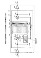
図8は、基幹光ネットワークにおける光分岐挿入装置の多段接続の例を示す図である。基幹光ネットワーク9は、光伝送路(光ファイバ140)上に光分岐挿入装置(OADM)10を複数N(10a〜10n)配置して光信号の伝送を行う。基幹光ネットワーク9は、例えば環状のリングネットワークによって構成されている。それぞれの光分岐挿入装置(OADM)10(10a〜10n)は、光ファイバ140から出力されたWDM光を増幅する光増幅器11と、WDM光の各チャンネル毎の光信号の分岐挿入を行う挿入分岐部20と、分岐挿入が行われたWDM光を増幅して光ファイバ140へ入力する光増幅器12とから構成されている。
FIG. 8 is a diagram illustrating an example of multistage connection of the optical add / drop multiplexers in the backbone optical network. The backbone
図8に示した基幹光ネットワーク9は、位置Aの光分岐挿入装置(OADM)10aにおいて5波の光信号が挿入(Add)され、位置Bの光分岐挿入装置(OADM)10bにおいて1波の光信号が挿入(Add)され、位置Nの光分岐挿入装置(OADM)10nにおいて、5波の光信号が分岐(Drop)される運用例を表している。基幹光ネットワーク9上の各光分岐挿入装置(OADM)10は、頻繁に光信号の分岐および挿入を行う。この他、位置Aと位置Bとの間(位置X)の光ファイバ140が破断し、位置B以降の光ファイバ140に伝送される光信号が1波だけになることもある。このように、運用波長数の変化が頻繁に生じた場合であっても、基幹光ネットワーク9(光分岐挿入装置10(10a〜10n))は、個々の光信号の通信品質を保つ必要がある。
In the backbone
通信品質を保つために、光分岐挿入装置(OADM)10の光増幅器11,12は、入力されたWDM光に対して利得一定制御を行う。具体的には、WDM光のなかの運用波長数にかかわらず、各信号の利得は同じ出力になるように制御を行っている。
In order to maintain communication quality, the
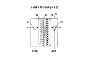
図9は、分岐挿入部の構成を示す図である。図9に示したような矢印方向AにWDM光の伝送が行われるとする。分岐挿入部20は、分岐ポート21と、分波器22と、光可変減衰器(VOA:Variable Optical Attenuator)23と、合波器24と、挿入ポート25とから構成されている。また、図10は、WDM光の出力の一例を示す図表であり、横軸は波長(λ)を表し、縦軸はWDM光の各光信号のパワー(Po)を表す。図表に示すようにWDM光は、波長(λa〜λn)毎の光信号と、全帯域に自然放出光(ASE:Amplified Spountaneous Emission)が雑音として蓄積された状態で伝送されている。
FIG. 9 is a diagram illustrating a configuration of the branch insertion unit. It is assumed that WDM light is transmitted in the arrow direction A as shown in FIG. The
図10に示したようなWDM光が光分岐挿入装置(OADM)10へ入力されると、光増幅器11によって増幅されたのち分岐挿入部20へ出力される。分岐挿入部20では、光信号の分岐も挿入も行わずに全ての光信号を透過したとすると、合波器24によって波長毎に分波され、光可変減衰器23へ入力される。このとき、光信号の波長(λa〜λn)以外の光は分波されないため、光信号の波長(λa〜λn)の近傍以外のASEが取り除かれる。光可変減衰器23は、入力された各波長(λa〜λn)の光信号を減衰することで信号波形の補正や出力レベル調整を行い、合波器24へ出力する。合波器24は、波長毎に分波された光信号を再び多重化して、光ファイバ140へ出力する。
When WDM light as shown in FIG. 10 is input to the optical add / drop device (OADM) 10, it is amplified by the
図11は、分岐挿入部から出力されたWDM光を示す図表であり、横軸は波長(λ)を表し、縦軸はWDM光の各光信号のパワー(Po)を表す。図11に示したように、分岐挿入部20から出力されたWDM光は、光信号(λa〜λn)と、各光信号の波長(λa〜λn)の近傍のASE(λa_ase〜λn_ase)とからなる。このように、ある一つの光分岐挿入装置(OADM)10単位でみると、各光信号の出力を一定にして通信品質を保つように構成されている(例えば、下記特許文献1参照。)。
FIG. 11 is a chart showing the WDM light output from the add / drop unit, where the horizontal axis represents the wavelength (λ) and the vertical axis represents the power (Po) of each optical signal of the WDM light. As shown in FIG. 11, the WDM light output from the add /
しかしながら、従来の光分岐挿入装置は、基幹光ネットワーク9上に多段接続された状態で、上記運用波長数が変化した場合、その直後における利得制御に過渡的な遅延が生じ、この過渡期間において通信品質が低下する問題があった。
However, when the number of operating wavelengths changes in a state where the conventional optical add / drop multiplexer is connected in multiple stages on the backbone
図12は、光増幅器に入力されるWDM光の運用波長数の変化の一例を示す説明図である。横軸は波長(λ)を表し、縦軸はWDM光の各光信号のパワー(Po)を表す。また、時期1201に示す状態の後、時間tが経過したときに時期1202に示す状態となったことを示している。例えば、光増幅器11もしくは光増幅器12へ入力されるWDM信号の運用波長数が、時期1201に示した6波(λa〜λf)の光信号から、時期1202に示した1波(λf)の光信号だけに変化した場合について説明する。
FIG. 12 is an explanatory diagram illustrating an example of a change in the number of operating wavelengths of WDM light input to the optical amplifier. The horizontal axis represents the wavelength (λ), and the vertical axis represents the power (Po) of each optical signal of the WDM light. In addition, after the state indicated by the
図13は、従来の光分岐挿入装置において、光信号が6波から1波へ変更された場合の波長の変化を示す図表である。横軸は波長(λ)を表し、縦軸はWDM光の各光信号のパワー(Po)を表す。時期1301に示す状態の後、時間tが経過したときに時期1302に示す状態となったことを示している。
FIG. 13 is a chart showing changes in wavelength when the optical signal is changed from 6 waves to 1 wave in the conventional optical add / drop multiplexer. The horizontal axis represents the wavelength (λ), and the vertical axis represents the power (Po) of each optical signal of the WDM light. After the state shown at
図12の時期1201に示したような6波(λa〜λf)の光信号からなるWDM光が光分岐挿入装置10に入力されたとする。光信号は、分波器22を経由すると、上述したように、光信号以外のASEが取り除かれるため、時期1301に示すように、光信号(λa〜λf)と、光信号(λa〜λf)の近傍のASE(λa_ase〜λf_ase)からなるWDM光が出力される。
It is assumed that WDM light composed of optical signals of six waves (λa to λf) as shown at
一方、WDM光の運用波長の数が変更されて図12の時期1202に示すような1波の光信号からなるWDM光が光分岐挿入装置10へ入力されたとする。このとき、光信号は、分波器22を経由すると、図13の時期1302に示すようなWDM光として出力される。時期1302では、波長λfの光信号と、波長λa〜λfそれぞれの近傍のASE(λa_ase〜λf_ase)がWDM光となり、このような波長の状態のWDM光が光増幅器12に入力される。このような場合、光増幅器12は、光信号の波長全体におけるパワーを検出して利得制御を行うため、光信号の波長数が1波になった直後には過渡的に、運用波長数が変わる直前の6波の光信号の状態における波長(λa〜λf)の近傍のASE(λa_ase〜λf_ase)のパワーを基準に利得が一定となる制御を行うことになる。
On the other hand, it is assumed that the number of operating wavelengths of the WDM light is changed and WDM light composed of one optical signal as shown at
図14は、図12に示した運用波長の変化における光増幅器の出力を示す説明図である。横軸は波長(λ)を表し、縦軸はWDM光の各光信号のパワー(Po)を表す。また、時期1401に示す状態の後、時間tが経過したときに時期1402に示す状態となったことを示している。図13に示した状態では、つまり、図14の時期1401に示すようなパワーを有していた6波(λa〜λf)のうち1波(λf)の光信号が所定のパワーがあったとする。
FIG. 14 is an explanatory diagram showing the output of the optical amplifier when the operating wavelength changes as shown in FIG. The horizontal axis represents the wavelength (λ), and the vertical axis represents the power (Po) of each optical signal of the WDM light. In addition, after the state indicated at
この後、運用波長数が変化して5波(λa〜λe)がなくなり、この1波(λf)だけになったとする。光増幅器11(12)は、この運用波長数が変化した直後の過渡応答期間中は、この1波(λf)が本来有していたパワーを、時期1402に示すパワーまで、矢印D分低減させてしまう。光増幅器11(12)は、時期1041に、全波長(λa〜λf)の平均する形で利得制御するため、時期1402における1波(λf)のパワーは、時期1401のときにパワーレベルがほぼ揃っていた5波(λa〜λe)のパワーレベルに引きずられて利得制御するからである。
Thereafter, it is assumed that the number of operating wavelengths is changed and five waves (λa to λe) disappear, and only one wave (λf) is present. During the transient response period immediately after the number of operating wavelengths changes, the optical amplifier 11 (12) reduces the power originally possessed by this one wave (λf) to the power indicated by the
このようなパワー、つまり利得の変動量は、一つの光分岐挿入装置10だけでみれば、わずかな利得変動量として無視できる。しかし、実際の基幹光ネットワーク9において光分岐挿入装置10が図8に示すように多段接続(10a〜10n)された場合、光分岐挿入装置10に挿入および分岐される、ある光信号の伝送経路の後段側にいくにしたがって、徐々にこの利得変動量が蓄積していくことになる。利得変動量の蓄積分が大きいと、光信号の利得が受信レンジよりも低下して信号として認識されず、受信エラーが生じる等、通信品質の低下を招く問題があった。
Such power, that is, a gain fluctuation amount, can be ignored as a slight gain fluctuation amount when only one optical add /
また、特許文献1の光分岐挿入装置の場合、利得レベルの低下を防ぐ機能を有しているが、そのためには、光分岐挿入装置内部に新たな光源を設置する必要があり、コストがかかり、なおかつ大型化するという問題があった。
In addition, the optical add / drop device disclosed in
この発明は、上述した従来技術による問題点を解消するため、運用波長数が変化したときの過渡的な利得変動を抑制し、光信号の通信品質を保つことができる光伝送装置を提供することを目的とする。 The present invention provides an optical transmission apparatus capable of suppressing the transient gain fluctuation when the number of operating wavelengths is changed and maintaining the communication quality of an optical signal in order to solve the above-described problems caused by the prior art. With the goal.
上述した課題を解決し、目的を達成するため、この発明にかかる光伝送装置は、入力光を分岐する分岐手段と、前記分岐手段の一方の分岐光から、信号光を含む帯域(λa〜λn)の光の出力レベルを調整し出力する光減衰手段と、前記分岐手段の他方の分岐光から、前記信号光を含む帯域以外(λa未満およびλnを超える波長)の光をバイパスさせるバイパス手段と、前記光減衰手段の出力と、前記バイパス手段の出力とを合波させる合波手段と、前記分岐手段の前段および前記合波手段の後段のうち少なくとも一方にそれぞれ配置される光増幅手段と、を備えたことを特徴とする。 In order to solve the above-described problems and achieve the object, an optical transmission apparatus according to the present invention includes a branching unit that branches input light, and a band (λa to λn) that includes signal light from one branching light of the branching unit. ) and light attenuation means for adjusting the output level of the optical output of the other branched light of said branch means and bypass means for bypassing the light other than the band including the signal light (wavelength greater than λa below and lambda] n) A multiplexing unit that combines the output of the optical attenuating unit and the output of the bypass unit, and an optical amplifying unit that is disposed at least one of the preceding stage of the branching unit and the subsequent stage of the multiplexing unit, It is provided with.
この発明によれば、信号光を含む帯域の光の出力レベルの調整とは別に、分岐された光信号から信号光の帯域外の光をバイパスさせて信号光の帯域の光と合波させるため、光増幅手段は、自然放出光を含む信号光を増幅でき、運用波長数が変化したときにおける増幅の利得変動を抑制する。 According to the present invention, separately from the adjustment of the output level of the light of the band including the signal light, the light outside the band of the signal light is bypassed from the branched optical signal and combined with the light of the signal light band. The optical amplifying means can amplify the signal light including the spontaneous emission light, and suppress the gain fluctuation of the amplification when the number of operating wavelengths is changed.
本発明にかかる光伝送装置によれば、運用波長数が変化したときでも利得変動量の蓄積による利得変動を抑制でき、光信号の通信品質を保つことができるという効果を奏する。 According to the optical transmission device of the present invention, even when the number of operating wavelengths is changed, gain fluctuation due to accumulation of gain fluctuation amount can be suppressed, and the communication quality of the optical signal can be maintained.
以下に添付図面を参照して、この発明にかかる光伝送装置の好適な実施の形態を詳細に説明する。以下の説明では、光伝送装置として光信号の分岐挿入を行う機能を有する光分岐挿入装置を例に説明する。 Exemplary embodiments of an optical transmission apparatus according to the present invention will be explained below in detail with reference to the accompanying drawings. In the following description, an optical add / drop device having a function of adding / dropping an optical signal will be described as an example of the optical transmission device.
図1は、本発明の実施の形態にかかる光分岐挿入装置の構成を示す図である。図1に示した光分岐挿入装置100は、図8に示したような基幹光ネットワーク9に複数配置してWDM信号を伝送するために用いる。光分岐挿入装置100は、光増幅器110,130と、光分岐挿入部120とによって構成され、光ファイバ140に接続されている。
FIG. 1 is a diagram illustrating a configuration of an optical add / drop multiplexer according to an embodiment of the present invention. A plurality of optical add /
光分岐挿入部120は、分岐(Drop)ポート121と、入力光を分岐する分岐手段としての光カプラ(1×2光カプラ)122と、分波器123と、信号光を含む帯域の光の出力レベルを調整する光減衰手段としての光可変減衰器(VOA)124と、合波器125と、信号帯域遮断フィルタ126と、光可変減衰器(VOA)127と、合波手段としての光カプラ(2×1光カプラ)128と、挿入(Add)ポート129とを備えている。
The optical add /
1×2光カプラ122は、入力光である光信号を2つに分岐させ、一方を分波器123に出力し、他方を信号帯域遮断フィルタ126に出力する。1×2光カプラ122によって分岐された一方(分波器123側)の経路R1は、光信号(信号光)を含む帯域の光の経路である。1×2光カプラ122によって分岐された他方(信号帯域遮断フィルタ126側)の経路R2は、光信号(信号光)の帯域外の光をバイパスさせるバイパス手段として機能する。
The 1 × 2
光伝送路としての光ファイバ140には特定の帯域の異なる波長(λa〜λn)の光信号が多重化されたWDM光として伝送されている。まず、光ファイバ140から、光分岐挿入装置100へWDM光が出力される。光分岐挿入装置100へ入力されたWDM光は、始めに光増幅器110へ入力される。光増幅器110は、入力されたWDM光の増幅を行い、光分岐挿入部120へ出力する。この光増幅器110は、入力されたWDM光の帯域、つまり、光信号の波長帯域(λa〜λn)よりも広い帯域の光を増幅するように設定されている。したがって、光信号の波長帯域よりも短波長および長波長域に含まれるASEに対しても増幅を行う。
An
図2は、光増幅器におけるWDM信号の増幅帯域を示す図表である。図表200において、横軸は波長(λ)を表し、縦軸はWDM光の各光信号のパワー(Po)を表す。一般的な光増幅器は、図表200に示した光信号増幅帯域Bのみを増幅させるものであるが、本発明(図1参照)の光増幅器110は、光信号増幅帯域B以外の帯域における点線で示した入力ASEを実線で示したような広い帯域に広げて増幅させる。このような光増幅器110は、内蔵されたフィルタの透過率(波長特性)を変更すること等によって得ることができる。
FIG. 2 is a chart showing the amplification band of the WDM signal in the optical amplifier. In the
図1に戻り説明を行うと、次に光分岐挿入部120へ出力されたWDM光は、分岐ポート121を経由して、1×2光カプラ122へ入力される。WDM光に多重された光信号のうち分岐させる光信号は、分岐ポート121から分岐される。1×2光カプラ122は、入力されたWDM光を2つに分波して、一方を分波器123へ出力し、他方を信号帯域遮断フィルタ126へ出力する。1×2光カプラ122は、WDM光に含まれる波長に関係なく光信号が多重されたまま複数に分波させる。
Returning to FIG. 1, the WDM light output to the optical add /
分波器123は、入力されたWDM光を波長毎(λa〜λn)の光信号に分波して、対応する光可変減衰器124へ出力する。光可変減衰器124は、分波された波長毎の複数(124a〜124n)を有し、それぞれ入力された光信号のレベル調整を行い、合波器125へ出力する。合波器125は、各光信号毎の光可変減衰器124から入力された光信号を合波し、再びWDM光として、2×1光カプラ128へ出力する。
The
一方、1×2光カプラ122によって、信号帯域遮断フィルタ126へ出力されたWDM光は、信号帯域遮断フィルタ126によって、光信号増幅帯域Bの波長(λa〜λn)の光のみが遮断される。これにより、光信号増幅帯域Bの波長(λa〜λn)以外の波長(λa未満およびλnを超える波長)のASE(ASE1およびASE2)を透過して光可変減衰器127へ出力させる。光可変減衰器127は、入力されたASEのレベル調整を行い、2×1光カプラ128へ出力する。なお、この光可変減衰器127を設けなくとも、光分岐挿入装置100を構成できる。
On the other hand, the WDM light output to the signal
なお、光可変減衰器127における減衰量の設定について、透過させるASEの透過率を高く設定しASEが高出力とした場合、ASEが伝送路で発振をおこし光信号に影響を与える。このため、光可変減衰器127は、ASEの透過率の上限を設定しておく。
In addition, regarding the setting of the attenuation amount in the optical
図3は、2×1光カプラによって合波された光信号とASEを示す図表である。図表300において、横軸は波長を表し、縦軸はWDM光の各光信号のパワーを表す。図1を用いて説明したように、2×1光カプラ128は、合波器125から出力されたWDM光(波長λa〜λn)と、分岐され光可変減衰器127から出力されたASE(ASE1,ASE2)との合波を行う。合波されたWDM光は図表300に示すように、光信号増幅帯域Bの波長(λa〜λn)の光信号と、光信号増幅帯域Bの外側の帯域のASE(ASE1,ASE2)とからなる。なお、上述したように、光信号増幅帯域Bの波長(λa〜λn)の光信号には、それぞれASE(λa_ase〜λn_ase)が含まれている。
FIG. 3 is a chart showing optical signals and ASE combined by the 2 × 1 optical coupler. In the
そして、2×1光カプラ128によって合波されたWDM光は、挿入ポート129を経由して、光増幅器130へ出力される。光信号が新たに挿入される場合は、光信号が挿入ポート129から挿入される。光増幅器130は、WDM信号の波長(λa〜λn)の光信号と、ASE(ASE1,ASE2)に対する増幅を行うため、光増幅器110と同様に、一般的な光増幅器よりも増幅帯域を拡張した設定になっている。増幅されたWDM光は、光ファイバ140へ出力される。光カプラ122の前段に配置される光増幅器110と、光カプラ128の後段に配置される光増幅器130は、いずれか一方だけを配置することもできる。
The WDM light combined by the 2 × 1
図4は、本発明にかかる光分岐挿入装置において、光信号が6波から1波へ変更された場合の波長の変化を示す図表である。横軸は、波長を表し、縦軸は光信号のパワーを表す。時期401に示す状態は、運用波長数が6波(λa〜λf)のある時期における光分岐挿入装置100の波長を表す。時期402に示す状態は、時期401から時間tが経過して運用波長数が1波(λf)のみに変化した状態を表している。
FIG. 4 is a chart showing changes in wavelength when the optical signal is changed from 6 waves to 1 wave in the optical add / drop multiplexer according to the present invention. The horizontal axis represents the wavelength, and the vertical axis represents the power of the optical signal. The state shown at
図4に示したように、ASE1,ASE2はそれぞれバックグラウンドとして、WDM光に残留する。分岐挿入装置100による分岐や、光ファイバ140の破断等により運用波長数が変化したとする。図示のように、時期401における運用波長数が6波(λa〜λf)の光信号の状態から5波(λa〜λe)の光信号が減り、時期402における運用波長数が1波(λfのみ)の光信号になったとする。この場合でも、光増幅器110,130は、バックグラウンドとしてのASE(ASE1,ASE2,λa_ase〜λn_ase)を基準として、1波(λf)の光信号のパワーにあわせた出力制御を行う。特に、運用波長数が変化する前後においてASE(ASE1,ASE2,λa_ase〜λn_ase)のパワーは変化しないため、利得の変動を抑制できる。
As shown in FIG. 4, ASE1 and ASE2 remain in the WDM light as backgrounds. It is assumed that the number of operating wavelengths has changed due to branching by the branching / inserting
図5は、従来の光分岐挿入装置における運用波長数変化に伴う利得変動量を示す図表である。また、図6は、本発明にかかる光分岐挿入装置における運用波長数変化に伴う利得変動量を示す図表である。図5および図6の各図表において、横軸は時間経過(t)を表し、縦軸はWDM光のパワー(Po)を表す。この図5および図6を用いて、上述した光分岐挿入装置100の利得制御について説明する。
FIG. 5 is a chart showing the amount of gain fluctuation accompanying the change in the number of operating wavelengths in a conventional optical add / drop multiplexer. FIG. 6 is a chart showing the amount of gain fluctuation accompanying the change in the number of operating wavelengths in the optical add / drop multiplexer according to the present invention. 5 and 6, the horizontal axis represents time (t), and the vertical axis represents WDM light power (Po). The gain control of the optical add /
図5に示す従来の光分岐挿入装置(例えば、図8に示した光分岐挿入装置10)におけるWDM光のパワーを表す図において、光増幅器12(減設が分岐による場合や光ファイバ140の破断が原因の場合は光増幅器11)による増幅前は、光増幅器12のパワー501は、減設する5波(chと同義:例えば図12の波長λa〜λe)分のパワーの変化を表している。5波(ch)分のパワーは、t1(減設時)を境にASE(λa_ase〜λe_ase)だけのパワーに低減する。一方、パワー502は、残留する1波(ch:図12の波長λf)分のパワーであり、一定のパワーが保たれることになる。したがって、特性線503に示すように、光増幅器12による増幅後の利得変動量ΔPoが大きい。
In the diagram showing the power of WDM light in the conventional optical add / drop device shown in FIG. 5 (for example, the optical add /
一方、本発明にかかる光分岐挿入装置100におけるWDM光のパワーを表す図6において、パワー801は、減設される5波(ch:例えば図4の波長λa〜λe)分のパワーの変化と、そのときのASE累積パワーを表している。t1(減設時)におけるパワー低減後、ASE累積パワーとの差が変動量となる。したがって、光増幅器120(減設が分岐による場合、光ファイバ140の破断が原因の場合は、光増幅器110)による増幅後のパワーを表す特性線802は、図5の特性線503に比して利得変動量ΔPoを減少させることができる。
On the other hand, in FIG. 6 showing the power of the WDM light in the optical add /
図7は、光分岐挿入装置を多段接続した場合の出力変動量を示す図表である。図表において、横軸は基幹光ネットワークにおいて多段接続されている光分岐挿入装置数を表し、縦軸は光分岐挿入装置におけるWDM光の運用波長数が5波から1波に変化した場合の出力変動量(dB)を表す。また、黒い四角でプロットした値は、従来の光分岐挿入装置10(図8参照)による特性線701であり、白い四角でプロットした値は、本発明にかかる光分岐挿入装置100(図1参照)による特性線702である。
FIG. 7 is a chart showing output fluctuation amounts when the optical add / drop multiplexer is connected in multiple stages. In the chart, the horizontal axis represents the number of optical add / drop multiplexers connected in multiple stages in the backbone optical network, and the vertical axis represents output fluctuations when the number of operating wavelengths of WDM light in the optical add / drop multiplexer changes from 5 waves to 1 wave. It represents the quantity (dB). The values plotted with black squares are
図7の特性線702から明らかなように、本発明にかかる光分岐挿入装置100は、光信号の帯域以外のASE(ASE1,ASE2、図4等参照)も透過させることで、WDM光の運用波長数が変化した場合の光信号のパワー変動量を減少させることができる。接続された光分岐挿入装置100の数が少ない場合は、出力変動量が小さいため、従来の光分岐挿入装置10との差はないが、光分岐挿入装置100の数が増える程、出力変動量は大きくなる。その結果、接続された光分岐挿入装置100の数が15台の場合、従来の光分岐挿入装置10と比較して、利得変動量は2.6(dB)程度改善することができた。
As is clear from the
また、本発明にかかる光分岐挿入装置100の場合、利得変動量を減少させるために新たな光源部を備える必要がなく、光カプラや(図1に記載の1×2光カプラ122や、2×1光カプラ128)、フィルタ(信号帯域遮断フィルタ126)を用いて、ASEを光源として利用するため、コストも低く抑えることが可能である。加えて、装置のサイズも従来の機能を有した光分岐挿入装置と変わらないサイズで実現することができる。
Further, in the case of the optical add /
以上説明したように、本発明にかかる光分岐挿入装置100は、上述したように運用波長数が変化したときに過渡的に生じる利得変動量を従来に比して大幅に改善することができる。したがって、都市間をつなぐ基幹光ネットワークにおいて光分岐挿入装置100が多段接続された場合であっても、通信品質を維持することができるようになる。
As described above, the optical add /
以上のように、本発明にかかる光伝送装置は、長距離伝送を行う基幹ネットワークに有用であり、特に、光分岐挿入装置が多段接続されるメトロコアに適している。 As described above, the optical transmission apparatus according to the present invention is useful for a backbone network that performs long-distance transmission, and is particularly suitable for a metro core in which optical add / drop multiplexers are connected in multiple stages.
100 光分岐挿入装置
110,130 光増幅器
120 光分岐挿入部
121 分岐ポート
122 1×2光カプラ
123 分波器
124,127 光可変減衰器
125 合波器
126 信号帯域遮断フィルタ
128 2×1光カプラ
129 挿入ポート
140 光伝送路(光ファイバ)
DESCRIPTION OF
Claims (5)
前記分岐手段の一方の分岐光から、信号光を含む帯域(λa〜λn)の光の出力レベルを調整し出力する光減衰手段と、
前記分岐手段の他方の分岐光から、前記信号光を含む帯域以外(λa未満およびλnを超える波長)の光をバイパスさせるバイパス手段と、
前記光減衰手段の出力と、前記バイパス手段の出力とを合波させる合波手段と、
前記分岐手段の前段および前記合波手段の後段のうち少なくとも一方にそれぞれ配置される光増幅手段と、
を備えたことを特徴とする光伝送装置。 A branching means for branching the input light;
An optical attenuating means for adjusting and outputting the output level of light in a band (λa to λn) including signal light from one branched light of the branching means;
Bypass means for bypassing light of a wavelength other than the band including the signal light (wavelength less than λa and greater than λn) from the other branched light of the branching means;
A multiplexing unit that combines the output of the light attenuating unit and the output of the bypass unit;
An optical amplifying means disposed in at least one of the preceding stage of the branching means and the subsequent stage of the multiplexing means;
An optical transmission device comprising:
前記信号光を含む帯域の光を遮断する信号帯域遮断フィルタを備えたことを特徴とする請求項1に記載の光伝送装置。 The bypass means includes
The optical transmission apparatus according to claim 1, further comprising a signal band cutoff filter that blocks light in a band including the signal light.
Priority Applications (2)
| Application Number | Priority Date | Filing Date | Title |
|---|---|---|---|
| JP2005100137A JP4557771B2 (en) | 2005-03-30 | 2005-03-30 | Optical transmission equipment |
| US11/319,362 US7650074B2 (en) | 2005-03-30 | 2005-12-29 | Optical transmission apparatus |
Applications Claiming Priority (1)
| Application Number | Priority Date | Filing Date | Title |
|---|---|---|---|
| JP2005100137A JP4557771B2 (en) | 2005-03-30 | 2005-03-30 | Optical transmission equipment |
Publications (2)
| Publication Number | Publication Date |
|---|---|
| JP2006279896A JP2006279896A (en) | 2006-10-12 |
| JP4557771B2 true JP4557771B2 (en) | 2010-10-06 |
Family
ID=37070619
Family Applications (1)
| Application Number | Title | Priority Date | Filing Date |
|---|---|---|---|
| JP2005100137A Expired - Fee Related JP4557771B2 (en) | 2005-03-30 | 2005-03-30 | Optical transmission equipment |
Country Status (2)
| Country | Link |
|---|---|
| US (1) | US7650074B2 (en) |
| JP (1) | JP4557771B2 (en) |
Families Citing this family (10)
| Publication number | Priority date | Publication date | Assignee | Title |
|---|---|---|---|---|
| JP4806640B2 (en) * | 2007-01-12 | 2011-11-02 | 日本放送協会 | Optical transmission equipment |
| JP5324660B2 (en) * | 2008-10-31 | 2013-10-23 | ヒューレット−パッカード デベロップメント カンパニー エル.ピー. | Prioritized optical arbitration system and method |
| JP5321041B2 (en) | 2008-12-24 | 2013-10-23 | 富士通株式会社 | Optical add / drop multiplexer and WDM transmission method |
| US8965207B2 (en) * | 2010-03-18 | 2015-02-24 | Orange | Method and device for inserting/extracting optical subband into multiband optical OFDM signal |
| EP2690800A4 (en) * | 2011-03-25 | 2014-10-29 | Nec Corp | Optical transmission device |
| US9794019B2 (en) | 2011-04-28 | 2017-10-17 | Hewlett Packard Enterprise Development Lp | Prioritized optical arbitration systems and methods |
| JP6050067B2 (en) * | 2012-09-18 | 2016-12-21 | Necエンジニアリング株式会社 | Optical transmission device and control method of optical transmission device |
| US10505626B2 (en) | 2015-06-30 | 2019-12-10 | Nec Corporation | Communication apparatus, communication method, and communication system |
| JP6578962B2 (en) * | 2016-01-25 | 2019-09-25 | 富士通株式会社 | Optical transmission device, optical transmission system, and optical signal output control method |
| WO2019003833A1 (en) * | 2017-06-27 | 2019-01-03 | 住友電気工業株式会社 | Optical receiver module, optical reception method, station-side device, pon system, and optical filter |
Citations (5)
| Publication number | Priority date | Publication date | Assignee | Title |
|---|---|---|---|---|
| JP2002353939A (en) * | 2001-05-25 | 2002-12-06 | Kddi Submarine Cable Systems Inc | Optical transmission device |
| JP2004527955A (en) * | 2001-03-30 | 2004-09-09 | マルコニ コミュニケイションズ ソシエタ ペル アチオニ | Survivable DWDM system |
| JP2006066946A (en) * | 2004-08-24 | 2006-03-09 | Nec Corp | Optical add-drop multiplexer and optical add-drop multiplexing method |
| JP2007526702A (en) * | 2004-03-05 | 2007-09-13 | エリクソン エービー | Add / drop type optical amplification device |
| JP2008504747A (en) * | 2004-06-25 | 2008-02-14 | タイコ テレコミュニケーションズ (ユーエス) インコーポレーテッド | Noise loaded optical fiber transmission system |
Family Cites Families (5)
| Publication number | Priority date | Publication date | Assignee | Title |
|---|---|---|---|---|
| US6233092B1 (en) | 1998-10-16 | 2001-05-15 | Corning Incorporated | Management and utilization of ASE in optical amplifier |
| JP3802992B2 (en) | 1999-02-08 | 2006-08-02 | 富士通株式会社 | WDM optical communication system |
| JP2001111495A (en) | 1999-10-04 | 2001-04-20 | Fujitsu Ltd | Light branching and inserting device and its control method |
| US7356259B1 (en) * | 2003-06-18 | 2008-04-08 | Ciena Corporation | Optical bypass upgrade configuration |
| JP4489522B2 (en) * | 2004-07-20 | 2010-06-23 | 富士通株式会社 | WDM optical transmission system |
-
2005
- 2005-03-30 JP JP2005100137A patent/JP4557771B2/en not_active Expired - Fee Related
- 2005-12-29 US US11/319,362 patent/US7650074B2/en active Active
Patent Citations (5)
| Publication number | Priority date | Publication date | Assignee | Title |
|---|---|---|---|---|
| JP2004527955A (en) * | 2001-03-30 | 2004-09-09 | マルコニ コミュニケイションズ ソシエタ ペル アチオニ | Survivable DWDM system |
| JP2002353939A (en) * | 2001-05-25 | 2002-12-06 | Kddi Submarine Cable Systems Inc | Optical transmission device |
| JP2007526702A (en) * | 2004-03-05 | 2007-09-13 | エリクソン エービー | Add / drop type optical amplification device |
| JP2008504747A (en) * | 2004-06-25 | 2008-02-14 | タイコ テレコミュニケーションズ (ユーエス) インコーポレーテッド | Noise loaded optical fiber transmission system |
| JP2006066946A (en) * | 2004-08-24 | 2006-03-09 | Nec Corp | Optical add-drop multiplexer and optical add-drop multiplexing method |
Also Published As
| Publication number | Publication date |
|---|---|
| US7650074B2 (en) | 2010-01-19 |
| JP2006279896A (en) | 2006-10-12 |
| US20060222366A1 (en) | 2006-10-05 |
Similar Documents
| Publication | Publication Date | Title |
|---|---|---|
| JP4557771B2 (en) | Optical transmission equipment | |
| US8204379B2 (en) | Noise reduction in optical communications networks | |
| JP4725951B2 (en) | Wavelength multiplexed signal light amplification method and optical amplifier | |
| US7650072B2 (en) | Method of upgrading optical node, and an optical node apparatus | |
| US7843631B2 (en) | Gain control apparatus, optical transmission apparatus, gain control method for optical amplifier, and wavelength multiplex optical transmission system | |
| JP4659498B2 (en) | Optical transmission equipment | |
| JP3769129B2 (en) | Optical amplifier and optical communication system having chromatic dispersion compensation function | |
| JP4930175B2 (en) | Node control device for transferring signal light | |
| JP5887698B2 (en) | Optical coupling / branching device and optical coupling / branching method | |
| JP4707542B2 (en) | Transmission equipment | |
| US6256140B1 (en) | Optical amplifying apparatus for transmitting wavelength division multiplexed signal light and optical network apparatus with using the same | |
| JP3938270B2 (en) | Optical repeater amplifier | |
| EP1788730B1 (en) | Optical amplification unit with span loss tilt compensation | |
| JP4522894B2 (en) | Wavelength division multiplexing communication system. | |
| JP7063329B2 (en) | Optical repeater, control method of optical repeater, and optical transmission system | |
| JP4234382B2 (en) | Optical amplification method, apparatus thereof, and optical amplification repeater system using the apparatus | |
| JP4806640B2 (en) | Optical transmission equipment | |
| JP2000004061A (en) | Optical gain equalization device | |
| JP3609968B2 (en) | Optical amplifier | |
| EP2071755B1 (en) | Optical Add-Drop Multiplexer | |
| EP1863202B1 (en) | An optical transmission system with gain adjustment | |
| JP4032551B2 (en) | WDM transmission system | |
| JP2006253782A (en) | Optical fiber communication system using distribution amplification | |
| WO2014017084A1 (en) | Wavelength division multiplexing optical transmission device for | |
| JP2004006888A (en) | Optical transmission device and multi-wavelength optical communication system |
Legal Events
| Date | Code | Title | Description |
|---|---|---|---|
| A621 | Written request for application examination |
Free format text: JAPANESE INTERMEDIATE CODE: A621 Effective date: 20080214 |
|
| A977 | Report on retrieval |
Free format text: JAPANESE INTERMEDIATE CODE: A971007 Effective date: 20100409 |
|
| A131 | Notification of reasons for refusal |
Free format text: JAPANESE INTERMEDIATE CODE: A131 Effective date: 20100413 |
|
| A521 | Request for written amendment filed |
Free format text: JAPANESE INTERMEDIATE CODE: A523 Effective date: 20100614 |
|
| TRDD | Decision of grant or rejection written | ||
| A01 | Written decision to grant a patent or to grant a registration (utility model) |
Free format text: JAPANESE INTERMEDIATE CODE: A01 Effective date: 20100713 |
|
| A01 | Written decision to grant a patent or to grant a registration (utility model) |
Free format text: JAPANESE INTERMEDIATE CODE: A01 |
|
| A61 | First payment of annual fees (during grant procedure) |
Free format text: JAPANESE INTERMEDIATE CODE: A61 Effective date: 20100720 |
|
| R150 | Certificate of patent or registration of utility model |
Ref document number: 4557771 Country of ref document: JP Free format text: JAPANESE INTERMEDIATE CODE: R150 Free format text: JAPANESE INTERMEDIATE CODE: R150 |
|
| FPAY | Renewal fee payment (event date is renewal date of database) |
Free format text: PAYMENT UNTIL: 20130730 Year of fee payment: 3 |
|
| LAPS | Cancellation because of no payment of annual fees |