JP4553185B2 - Semiconductor integrated circuit device - Google Patents
Semiconductor integrated circuit device Download PDFInfo
- Publication number
- JP4553185B2 JP4553185B2 JP2004267645A JP2004267645A JP4553185B2 JP 4553185 B2 JP4553185 B2 JP 4553185B2 JP 2004267645 A JP2004267645 A JP 2004267645A JP 2004267645 A JP2004267645 A JP 2004267645A JP 4553185 B2 JP4553185 B2 JP 4553185B2
- Authority
- JP
- Japan
- Prior art keywords
- power supply
- memory cell
- circuit
- signal
- mosfet
- Prior art date
- Legal status (The legal status is an assumption and is not a legal conclusion. Google has not performed a legal analysis and makes no representation as to the accuracy of the status listed.)
- Active
Links
Images


Classifications
-
- H—ELECTRICITY
- H10—SEMICONDUCTOR DEVICES; ELECTRIC SOLID-STATE DEVICES NOT OTHERWISE PROVIDED FOR
- H10B—ELECTRONIC MEMORY DEVICES
- H10B99/00—Subject matter not provided for in other groups of this subclass
-
- G—PHYSICS
- G11—INFORMATION STORAGE
- G11C—STATIC STORES
- G11C11/00—Digital stores characterised by the use of particular electric or magnetic storage elements; Storage elements therefor
- G11C11/21—Digital stores characterised by the use of particular electric or magnetic storage elements; Storage elements therefor using electric elements
- G11C11/34—Digital stores characterised by the use of particular electric or magnetic storage elements; Storage elements therefor using electric elements using semiconductor devices
- G11C11/40—Digital stores characterised by the use of particular electric or magnetic storage elements; Storage elements therefor using electric elements using semiconductor devices using transistors
- G11C11/41—Digital stores characterised by the use of particular electric or magnetic storage elements; Storage elements therefor using electric elements using semiconductor devices using transistors forming static cells with positive feedback, i.e. cells not needing refreshing or charge regeneration, e.g. bistable multivibrator or Schmitt trigger
- G11C11/412—Digital stores characterised by the use of particular electric or magnetic storage elements; Storage elements therefor using electric elements using semiconductor devices using transistors forming static cells with positive feedback, i.e. cells not needing refreshing or charge regeneration, e.g. bistable multivibrator or Schmitt trigger using field-effect transistors only
-
- G—PHYSICS
- G11—INFORMATION STORAGE
- G11C—STATIC STORES
- G11C11/00—Digital stores characterised by the use of particular electric or magnetic storage elements; Storage elements therefor
- G11C11/21—Digital stores characterised by the use of particular electric or magnetic storage elements; Storage elements therefor using electric elements
- G11C11/34—Digital stores characterised by the use of particular electric or magnetic storage elements; Storage elements therefor using electric elements using semiconductor devices
- G11C11/40—Digital stores characterised by the use of particular electric or magnetic storage elements; Storage elements therefor using electric elements using semiconductor devices using transistors
- G11C11/41—Digital stores characterised by the use of particular electric or magnetic storage elements; Storage elements therefor using electric elements using semiconductor devices using transistors forming static cells with positive feedback, i.e. cells not needing refreshing or charge regeneration, e.g. bistable multivibrator or Schmitt trigger
- G11C11/413—Auxiliary circuits, e.g. for addressing, decoding, driving, writing, sensing, timing or power reduction
- G11C11/417—Auxiliary circuits, e.g. for addressing, decoding, driving, writing, sensing, timing or power reduction for memory cells of the field-effect type
- G11C11/419—Read-write [R-W] circuits
-
- G—PHYSICS
- G11—INFORMATION STORAGE
- G11C—STATIC STORES
- G11C5/00—Details of stores covered by group G11C11/00
- G11C5/06—Arrangements for interconnecting storage elements electrically, e.g. by wiring
- G11C5/063—Voltage and signal distribution in integrated semi-conductor memory access lines, e.g. word-line, bit-line, cross-over resistance, propagation delay
-
- G—PHYSICS
- G11—INFORMATION STORAGE
- G11C—STATIC STORES
- G11C5/00—Details of stores covered by group G11C11/00
- G11C5/14—Power supply arrangements, e.g. power down, chip selection or deselection, layout of wirings or power grids, or multiple supply levels
-
- H—ELECTRICITY
- H10—SEMICONDUCTOR DEVICES; ELECTRIC SOLID-STATE DEVICES NOT OTHERWISE PROVIDED FOR
- H10B—ELECTRONIC MEMORY DEVICES
- H10B10/00—Static random access memory [SRAM] devices
-
- H—ELECTRICITY
- H10—SEMICONDUCTOR DEVICES; ELECTRIC SOLID-STATE DEVICES NOT OTHERWISE PROVIDED FOR
- H10B—ELECTRONIC MEMORY DEVICES
- H10B10/00—Static random access memory [SRAM] devices
- H10B10/12—Static random access memory [SRAM] devices comprising a MOSFET load element
Landscapes
- Engineering & Computer Science (AREA)
- Microelectronics & Electronic Packaging (AREA)
- Computer Hardware Design (AREA)
- Power Engineering (AREA)
- Static Random-Access Memory (AREA)
- Semiconductor Memories (AREA)
Description
本発明は、半導体集積回路装置に関し、特に、スタティック型RAM(ランダム・アクセス・メモリ)を備えたものに利用して有効な技術に関するものである。 The present invention relates to a semiconductor integrated circuit device, and more particularly to a technique effective when used for a device having a static RAM (random access memory).
スタティック型RAM(以下、単にSRAMという)のメモリセルの特性にスタティツクノイズマージン(以下SNMという)がある。SNMはメモリセルに記憶したデータの安定性を示するものであり、大きいほどデータ保持動作が安定するが、反面では保持データに対して逆データを書き込むときには書き込みにくくなる。かかる問題を解決する技術として、特開2002−042476公報がある。図17には上記公報に基づいて本願発明者が先に検討したSRAMのブロック図が示されている。この公報の技術では、読み出し時には、図18に示したような電圧供給回路を用い、信号WEiをロウレベルにすることでPチャネルMOSFETをオン状態にして外部電源Vccと同レベルの電圧をメモリセルに供給し安定駆動する。書き込み時には、上記信号WEiをハイレベルにすることで上記PチャネルMOSFETをオフ状態にし、代わってNチャネルMOSFETをオン状態にしてメモリセルに供給する内部電源をVcc−Vthに低下させる。これにより、ワード線により選択させたメモリセルのSNMが低下し、書き込みマージンを向上することができる。
上記特許文献1の技術では、行デコードにより選択されワード線が活性化されたメモリセルのうち、列デコードによって選択されないメモリセルについても内部電源が低下し、且、書き込み動作を行わないためにSNMが低下した読み出し状態となり、ノイズ等の影響を受けてデータ消失の危険性がある。かかる危険を回避するために上記特許文献1では、図19に示したような外部電源電圧御回路により下限電圧を設定し、これを判別することで上記非選択メモリセルのSNMが低下を制限するようにするものである。しかしながら、上記のような下限電圧を発生させるためには、メモリ内部に中間的な電源発生回路を設けることが必要となりメモリ回路の消費電流を増大させてしまうことと、上記下限電圧により上記SNMの低下が制限されてしまい、書き込みマージンを向上させることができない。特に、LSI(Large Scale Integrated circuit:大規模集積回路) では、低消費電力化およびLSI中のトランジスタ(MOSFET)の微細化により、電源電圧を低下させる傾向にあり、上記下限電圧との差が小さくなる。メモリ回路としては、上記SNMを優先させることが必要となり、上記引用文献1の技術では書き込みマージンの向上が望めない場合がある。
In the technique of
この発明の目的は、低電源電圧でもSNMと書き込みマージンを両立させることができるスタティック型RAMを備えて半導体集積回路装置を提供することにある。この発明の前記ならびにそのほかの目的と新規な特徴は、本明細書の記述および添付図面から明らかになるであろう。 An object of the present invention is to provide a semiconductor integrated circuit device including a static RAM that can achieve both SNM and write margin even at a low power supply voltage. The above and other objects and novel features of the present invention will be apparent from the description of this specification and the accompanying drawings.
本願において開示される発明のうち代表的なものの概要を簡単に説明すれば、下記の通りである。複数のワード線と複数の相補ビット線に対応して設けられた複数のスタティック型メモリセルを備え、上記複数の相補ビット線のそれぞれに接続される複数からなるメモリセル毎に動作電圧を供給する複数のメモリセル電源線を設け、かかるメモリセル電源線に対応してそれぞれ電源電圧を供給する抵抗手段からなる複数の電源供給回路を設け、上記相補ビット線に上記電源電圧に対応したプリチャージ電圧を供給するプリチャージ回路を設け、上記メモリセル電源線は、対応する相補ビット線の書き込み信号が伝えられる結合容量を持つようにする。 The outline of a typical invention among the inventions disclosed in the present application will be briefly described as follows. A plurality of static memory cells provided corresponding to a plurality of word lines and a plurality of complementary bit lines are provided, and an operating voltage is supplied to each of the plurality of memory cells connected to each of the plurality of complementary bit lines. A plurality of power supply circuits comprising resistor means for supplying a plurality of memory cell power supply lines and corresponding to each of the memory cell power supply lines are provided, and a precharge voltage corresponding to the power supply voltage is provided on the complementary bit line. The memory cell power supply line has a coupling capacity capable of transmitting a write signal of the corresponding complementary bit line.
本願において開示される発明のうち他の代表的なものの概要を簡単に説明すれば、下記の通りである。複数のワード線と複数の相補ビット線に対応して設けられた複数のスタティック型メモリセルを備え、上記複数の相補ビット線のそれぞれに接続される複数からなるメモリセル毎に動作電圧を供給する複数のメモリセル電源線を設け、かかるメモリセル電源線に対応して書き込み時にオフ状態にされるスイッチMOSFETからなる複数の電源供給回路を設ける。 The outline of other representative ones of the inventions disclosed in the present application will be briefly described as follows. A plurality of static memory cells provided corresponding to a plurality of word lines and a plurality of complementary bit lines are provided, and an operating voltage is supplied to each of the plurality of memory cells connected to each of the plurality of complementary bit lines. A plurality of memory cell power supply lines are provided, and a plurality of power supply circuits including switch MOSFETs that are turned off at the time of writing are provided corresponding to the memory cell power supply lines.
選択された相補ビット線に対応したメモリセルの書き込み動作マージンの向上を図りつつ、上記非選択相補ビット線に接続される非選択メモリセルのSNMを確保することができる。 While improving the write operation margin of the memory cell corresponding to the selected complementary bit line, the SNM of the non-selected memory cell connected to the non-selected complementary bit line can be secured.
図1には、この発明に係るスタティック型RAMの一実施例のブロック図が示されている。同図には、4つのメモリセル、それに対応した2つのワード線WL0とWLn、相補ビット線/BL0,BL0と/BLm,BLmが代表として例示的に示されている。メモリセルは、図示しないけれども、PチャネルMOSFETとNチャネルMOSFETからなる2つのCMOSインバータ回路の入力と出力とを交差接続してラッチ(フリップフロップ)回路を構成して記憶部とし、かかる入出力相互接続部を記憶ノードとして、対応するビット線/BLとBLとの間に設けられたアドレス選択用のNチャネルMOSFETから構成される。このアドレス選択用のMOSFETのゲートは、対応するワード線に接続される。 FIG. 1 is a block diagram showing an embodiment of a static RAM according to the present invention. In the drawing, four memory cells, two corresponding word lines WL0 and WLn, and complementary bit lines / BL0, BL0 and / BLm, BLm are exemplarily shown as representatives. Although not shown, the memory cell forms a latch (flip-flop) circuit by cross-connecting the inputs and outputs of two CMOS inverter circuits composed of a P-channel MOSFET and an N-channel MOSFET to form a memory unit, and this input / output mutual Using the connection portion as a storage node, it is composed of an N-channel MOSFET for address selection provided between the corresponding bit lines / BL and BL. The gate of this address selection MOSFET is connected to the corresponding word line.
ワード線WL0〜Wnのうち、1つが行デコーダによって選択される。行デコーダには、後述するようなワードドライバを備える。行デコーダには、アドレス信号のうちのロウ(行)系アドレス信号が供給される。複数の相補ビット線/BL0,BL0〜/BLm,BLmのうち、一対が列選択スイッチを介して書込ドライバ又はセンスアンプに接続される。つまり、列選択スイッチは、列デコーダにより形成される選択信号YS0〜YSmを受けて、上記複数の相補ビット線/BL0,BL0〜/BLm,BLmのうちの一対を選択して上記書込バッファの出力端子、センスアンプの入力端子に接続させる。 One of the word lines WL0 to Wn is selected by the row decoder. The row decoder includes a word driver as will be described later. The row decoder is supplied with a row (row) address signal among the address signals. Of the plurality of complementary bit lines / BL0, BL0 / BLm, BLm, a pair is connected to a write driver or a sense amplifier via a column selection switch. That is, the column selection switch receives the selection signals YS0 to YSm formed by the column decoder, selects a pair of the plurality of complementary bit lines / BL0, BL0 to / BLm, BLm and Connect to the output terminal and the input terminal of the sense amplifier.
制御回路には、読/書制御信号R/Wが供給される。制御回路は、読/書制御信号R/Wに対応して書込信号WE又は読出信号としてのセンスアンプ制御信号SACを発生させる。上記書込信号WEは、書込ドライバに供給されて書込ドライバを活性化するために用いられる。つまり、行デコーダによりワード線の1つが選択され、列デコーダにより一対の相補ビット線が列選択スイッチにより選択され、書込ドライバが活性化されたなら、データ入力信号が選択ワード線と選択相補ビット線に結合されたメモリセルに書き込まれる。上記センスアンプ制御信号SACは、センスアンプを活性化するために用いられる。上記同様に行デコーダによりワード線の1つが選択され、列デコーダにより一対の相補ビット線が列選択スイッチにより選択され、センスアンプが活性化されたなら、選択ワード線と選択相補ビット線に結合されたメモリセルの読み出し信号がセンスアンプに伝えられて増幅されてデータ出力として読み出される。 A read / write control signal R / W is supplied to the control circuit. The control circuit generates a write signal WE or a sense amplifier control signal SAC as a read signal in response to the read / write control signal R / W. The write signal WE is supplied to the write driver and used to activate the write driver. That is, when one of the word lines is selected by the row decoder, a pair of complementary bit lines are selected by the column decoder by the column selection switch, and the write driver is activated, the data input signal is selected by the selected word line and the selected complementary bit. Write to memory cells coupled to the line. The sense amplifier control signal SAC is used to activate the sense amplifier. Similarly to the above, if one of the word lines is selected by the row decoder, a pair of complementary bit lines are selected by the column selection switch by the column decoder, and the sense amplifier is activated, the selected word line and the selected complementary bit line are coupled. The read signal of the memory cell transmitted to the sense amplifier is amplified and read as a data output.
この実施例では、選択された相補ビット線に対応したメモリセルの書き込み動作マージンの向上を図りつつ、上記非選択相補ビット線に接続される非選択メモリセルのSNMを確保するために、相補ビット線/BL0,BL0〜/BLm,BLmのそれぞれに対応してメモリセル電源線VCC0〜VCCmを設ける。つまり、代表として例示的に示されているメモリセル電源線VCC0は、対応する相補ビット/BL0,BL0に接続されるメモリセルの電源線とされる。同様に、代表として例示的に示されているメモリセル電源線VCCmは、対応する相補ビット/BLm,BLmに接続されるメモリセルの電源線とされる。そしで、上記各メモリセル電源線VCC0〜VCCmと電源VCCとの間には、電源回路0〜mが設けられる。
In this embodiment, in order to secure the SNM of the non-selected memory cell connected to the non-selected complementary bit line while improving the write operation margin of the memory cell corresponding to the selected complementary bit line, Memory cell power supply lines VCC0 to VCCm are provided corresponding to lines / BL0, BL0 to / BLm and BLm, respectively. That is, the memory cell power supply line VCC0 exemplarily shown as a representative is a power supply line of a memory cell connected to the corresponding complementary bits / BL0 and BL0. Similarly, the memory cell power supply line VCCm shown as a representative example is a power supply line of a memory cell connected to the corresponding complementary bit / BLm, BLm. Therefore,
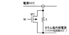
図2には、図1の電源回路の一実施例の回路図が示されている。この実施例では、電源回路として、PチャネルMOSFETQPが用いられる。このMOSFETQPのゲートには、回路の接地電位が定常的に与えられて抵抗素子として動作し、電源VCCをカラム毎内部電源、つまりはメモリセル電源線に伝える。このMOSFETQPのオン抵抗値は、次に説明するようにメモリセルへの書き込み動作のために相補ビット線/BL又はBLの一方が電源電圧VCCのようなプリチャージレベルから回路の接地電位のようなロウレベルに変化したとき、かかる変化したビット線の電位との容量結合によって上記メモリセル電源線の電位が一時的に低下することを許容する程度の比較的大きな抵抗値を持つようにされる。このような書き込みメモリセルへの動作電位の低下によって上記SNMを低下させて書き込みマージンを向上させる。これに対して、非選択のビット線/BLとBLはいずれも電源電圧VCCのようなハイレベルに維持されるから、それに対応したメモリセル電源線も電源電圧VCCに維持される。したがって、ワード線が選択状態にされたメモリセルにおいても、上記電源電圧が高く維持されるからSNMを高く維持することができる。 FIG. 2 shows a circuit diagram of an embodiment of the power supply circuit of FIG. In this embodiment, a P-channel MOSFET QP is used as the power supply circuit. The gate of the MOSFET QP is steadily given a circuit ground potential and operates as a resistance element to transmit the power supply VCC to the internal power supply for each column, that is, the memory cell power supply line. The on-resistance value of the MOSFET QP is such that one of the complementary bit lines / BL or BL is changed from the precharge level such as the power supply voltage VCC to the ground potential of the circuit for the write operation to the memory cell as described below. When the level is changed to a low level, the resistance of the memory cell power supply line is allowed to be temporarily lowered by capacitive coupling with the changed potential of the bit line. By reducing the operating potential to the write memory cell, the SNM is lowered to improve the write margin. On the other hand, since the unselected bit lines / BL and BL are both maintained at a high level like the power supply voltage VCC, the corresponding memory cell power supply line is also maintained at the power supply voltage VCC. Therefore, even in the memory cell in which the word line is selected, the SNM can be maintained high because the power supply voltage is maintained high.
図3には、この発明に係るメモリセルの一実施例の回路図が示されている。メモリセルは、PチャネルMOSFETQ1とNチャネルMOSFETQ2及びPチャネルMOSFETQ3とNチャネルMOSFETQ4とから2つのCMOSインバータ回路の入力と出力とを交差接続してラッチ(フリップフロップ)回路を構成して記憶部とし、かかる入出力相互接続部を記憶ノードN1、N2として、対応するビット線/BLとBLとの間に設けられたアドレス選択用のNチャネルMOSFETQ5とQ6から構成される。これらのアドレス選択用のMOSFETQ5、Q6のゲートは、対応するワード線WLに接続される。 FIG. 3 is a circuit diagram showing one embodiment of a memory cell according to the present invention. The memory cell comprises a latch (flip-flop) circuit by cross-connecting the input and output of two CMOS inverter circuits from the P-channel MOSFET Q1, the N-channel MOSFET Q2, the P-channel MOSFET Q3, and the N-channel MOSFET Q4 to form a memory unit, Such input / output interconnections are constituted by storage nodes N1 and N2 and N channel MOSFETs Q5 and Q6 for address selection provided between corresponding bit lines / BL and BL. The gates of these address selecting MOSFETs Q5 and Q6 are connected to the corresponding word line WL.
この実施例のメモリセルでは、相補ビット線/BLとBLに対応したメモリセルへの動作電圧VCC’の供給は、かかる相補ビット線/BLとBLとの間に設けられて、これらと平行に延長されるメモリセル電源線から供給される。つまり、上記メモリセル電源線は、上記CMOSインバータ回路を構成するPチャネルMOSFETQ1とQ3のソースに接続される。上記のようなメモリセル電源線は、上記相補ビット線の一方/BLとの間に寄生容量C1を持ち、相補ビット線の他方BLとの間に寄生容量C2を持つ。 In the memory cell of this embodiment, the supply of the operating voltage VCC ′ to the memory cells corresponding to the complementary bit lines / BL and BL is provided between the complementary bit lines / BL and BL, and in parallel therewith. Supplied from the extended memory cell power line. That is, the memory cell power supply line is connected to the sources of P-channel MOSFETs Q1 and Q3 constituting the CMOS inverter circuit. The memory cell power line as described above has a parasitic capacitance C1 between one of the complementary bit lines / BL and a parasitic capacitance C2 between the other BL of the complementary bit lines.
図4には、この発明に係るメモリセルの一実施例のレイアウト図が示されている。図4の(A)には、MOSFETのソース、ドレイン及びゲート及びコンタクト用配線及びコンタクトホールの各レイアウトパターンが示され、図4(B)には、ビット線/BL,BL及びメモリセルの動作電圧VCC’を供給するメモリセル電源線とコンタクト用配線及びコンタクトホールのレイアウトパターンが示され、図4(C)には、ワード線WLとメモリセルに接地電位VSSを供給する接地線及びコンタクトホールのレイアウトパターンが示されている。コンタクトホールは、各(A)(B)(C)に代表として1つが示されているCNTのように四角に×印を付すことにより示されている。 FIG. 4 shows a layout diagram of an embodiment of the memory cell according to the present invention. 4A shows each layout pattern of the source, drain and gate of MOSFET, contact wiring and contact hole, and FIG. 4B shows the operation of bit lines / BL, BL and memory cells. The layout pattern of the memory cell power supply line for supplying the voltage VCC ′, the contact wiring, and the contact hole is shown. FIG. 4C shows the ground line and contact hole for supplying the ground potential VSS to the word line WL and the memory cell. The layout pattern is shown. A contact hole is indicated by attaching a cross to a square like a CNT, one representative of which is shown in each of (A), (B), and (C).
図4(A)において、PチャネルMOSFETQ1とQ3は、斜線を付した中央部分に設けられたN型ウェルNWELに形成される。これに対して、NチャネルMOSFETQ2、Q4及びQ5とQ6は、上記N型ウェルNWELの部分以外のP型基板又はP型ウェルPWELに形成される。上記CMOSインバータ回路を構成するMOSFETQ1とQ2及びQ3とQ4のそれぞれは、ゲート電極が一体的に形成される。各コンタクト用配線及びコンタクトホールには、接続先がWL、/BL、VCC’、BL、WL及びVSSのように示されている。MOSFETQ1とQ2及びQ5と、MOSFETQ2、Q4及びQ6は、メモリセルの中点部を基準にして180°回転させた位置に対称的に配置される。コンタクト用の配線層は、コンタクトホールを囲む白抜きのパターンで示されており、特に制限されないが、第1層目のメタル層M1から構成される。 In FIG. 4A, P-channel MOSFETs Q1 and Q3 are formed in an N-type well NWEL provided in a hatched central portion. On the other hand, the N-channel MOSFETs Q2, Q4 and Q5 and Q6 are formed on the P-type substrate or the P-type well PWEL other than the portion of the N-type well NWEL. Each of MOSFETs Q1 and Q2 and Q3 and Q4 constituting the CMOS inverter circuit is integrally formed with a gate electrode. In each contact wiring and contact hole, connection destinations are shown as WL, / BL, VCC ′, BL, WL, and VSS. MOSFETs Q1, Q2, and Q5 and MOSFETs Q2, Q4, and Q6 are symmetrically arranged at positions rotated by 180 ° with respect to the middle point of the memory cell. The contact wiring layer is shown by a white pattern surrounding the contact hole, and is not particularly limited, but is composed of the first metal layer M1.
図4(B)において、ビット線/BL,BLは、それが接続されるMOSFETQ5及びQ6の一方のソース,ドレインに対応し、凡そメモリセル領域を同図において横方向に四等分する境界線のうちの1/4と3/4の部分に同図において縦方向に延長されるように配置され、特に制限されないが、第2層目のメタル配線層M2により形成される。メモリセル電源線も上記ビット線/BL,BLと同じ第2層目のメタル層M2により形成され、上記凡そメモリセル領域を四等分する境界線のうちの中央(2/4)の部分に縦方向に延長されるように設けられる。そして、メモリセル電源線(VCC’)は、上部においてPチャネルMOSFETQ1のソースと接続させるために隣接するビット線/BLの方向に延びる突起部を有し、下部においてPチャネルMOSFETQ3のソースと接続させるために隣接するビット線BLの方向に延びる突起部を有する。このような配線レイアウトによって、ビット線/BLとメモリセル電源線(VCC’)との間には、寄生容量C1が形成されることなり、ビット線BLとメモリセル電源線(VCC’)との間には、寄生容量C2が形成されることなる。 In FIG. 4B, bit lines / BL and BL correspond to one source and drain of MOSFETs Q5 and Q6 to which the bit lines / BL and BL are connected, and are boundary lines that divide the memory cell region into four equal parts in the horizontal direction in FIG. Among them, 1/4 and 3/4 portions are arranged so as to extend in the vertical direction in the figure, and are not particularly limited, but are formed by the second metal wiring layer M2. The memory cell power supply line is also formed by the second metal layer M2 which is the same as the bit lines / BL and BL, and is formed at the center (2/4) of the boundary line which divides the memory cell region into four equal parts. It is provided to extend in the vertical direction. The memory cell power line (VCC ′) has a protrusion extending in the direction of the adjacent bit line / BL in order to be connected to the source of the P-channel MOSFET Q1 in the upper part, and connected to the source of the P-channel MOSFET Q3 in the lower part. Therefore, a protrusion extending in the direction of the adjacent bit line BL is provided. With such a wiring layout, a parasitic capacitance C1 is formed between the bit line / BL and the memory cell power supply line (VCC ′), and the bit line BL and the memory cell power supply line (VCC ′) A parasitic capacitance C2 is formed between them.
図4(C)において、ワード線WLはメモリセル領域の中央部を同図の横方向に延長される。このワード線WLは、第3層目のメタル層M3により形成される。そして、メモリセル領域に設けられ、縦方向に延長されるよう設けられるのは、メモリセルの接地線VSSであり、第4層目のメタル層M4から構成される。この接地線VSSは、隣接するメモリセルの接地線VSSと共用される。この実施例のようなメモリセル構成とすることにより、カラム毎に電源線を形成することが容易になる。そして、ビット線/BL、BLと内部電源線(メモリセル電源線)との間にカップリング容量C1,C2を形成することができる。 In FIG. 4C, the word line WL extends in the horizontal direction in the figure at the center of the memory cell region. The word line WL is formed by the third metal layer M3. The memory cell ground line VSS provided in the memory cell region and extending in the vertical direction is composed of a fourth metal layer M4. This ground line VSS is shared with the ground line VSS of the adjacent memory cell. With the memory cell configuration as in this embodiment, it is easy to form a power supply line for each column. Then, coupling capacitors C1 and C2 can be formed between the bit lines / BL and BL and the internal power supply line (memory cell power supply line).
図5には、この発明に係るスタティック型RAMの動作の一例を説明するための波形図が示されている。スタティック型RAMの読み出し時には、ワード線WLの選択動作によって、前記メモリセルのアドレス選択MOSFETQ5とQ6がオン状態となり、メモリセルの記憶ノードN1とN2のうちロウレベルにされたノードに対応してビット線/BLとBLの一方が低下する。このとき、ビット線/BLとBLには、多数のメモリセルが接続されることによって比較的大きな寄生容量を持ち、上記アドレス選択MOSFETQ5、Q6のオン抵抗値は比較的大きいから上記ビット線/BLとBLの読み出し信号の低下は小さくてそのレベル変化も緩やかである。それ故、前記のようにビット線/BLとBLとメモリセル電源線との間に寄生容量(カップリング容量)C1とC2が存在しても、メモリセル電源線の電圧VCC’は殆ど変化せず電源電圧VCCを維持する。これにより、読み出し動作時のスタティツクノイズマージン(SNM)は大きく維持することができる。上記のようなビット線/BLとBLの小さなレベル差の読み出し信号は、センスアンプにより増幅されてデータ出力として出力される。 FIG. 5 is a waveform diagram for explaining an example of the operation of the static RAM according to the present invention. At the time of reading from the static RAM, the address selection MOSFETs Q5 and Q6 of the memory cell are turned on by the selection operation of the word line WL, and the bit line corresponding to the low level node among the storage nodes N1 and N2 of the memory cell. One of / BL and BL decreases. At this time, the bit lines / BL and BL have a relatively large parasitic capacitance by being connected to a large number of memory cells, and the on-resistance values of the address selection MOSFETs Q5 and Q6 are relatively large. The decrease in the read signal of BL is small and its level change is also gradual. Therefore, even if the parasitic capacitances (coupling capacitances) C1 and C2 exist between the bit lines / BL and BL and the memory cell power supply line as described above, the voltage VCC ′ of the memory cell power supply line hardly changes. First, the power supply voltage VCC is maintained. As a result, the static noise margin (SNM) during the read operation can be kept large. A read signal having a small level difference between the bit lines / BL and BL as described above is amplified by a sense amplifier and output as a data output.
スタティック型RAMの書き込み時には、ワード線WLの選択動作によって、前記メモリセルのアドレス選択MOSFETQ5とQ6がオン状態となっている。そして、書込ドライバからの書き込み信号に対応してビット線/BLとBLの一方が急激に回路の接地電位まで低下する。このようなフル振幅の書き込み信号の低下は、メモリセル電源線との間に寄生容量(カップリング容量)C1又はC2を介してメモリセル電源線に伝えられてメモリセルの動作電圧VCC’を一時的に低下させる。つまり、動作電圧VCC’は上記カップリングによって低下するが、電源回路としての抵抗素子を介して電源電圧VCCが供給されるので徐々に電源電圧VCCに向かって回復する。このときには、ビット線/BL又はBLの一方がロウレベルになっており、上記ワード線の選択状態によりオン状態になっているMOSFETQ5又はQ6を通して、記憶ノードN1又はN2のハイレベルをロウレベルに引き抜くので、メモリセルの記憶部の記憶情報が反転させられる。 At the time of writing to the static RAM, the address selection MOSFETs Q5 and Q6 of the memory cell are turned on by the selection operation of the word line WL. In response to a write signal from the write driver, one of the bit lines / BL and BL suddenly drops to the ground potential of the circuit. Such a decrease in the full-amplitude write signal is transmitted to the memory cell power supply line via the parasitic capacitance (coupling capacitance) C1 or C2 between the memory cell power supply line and temporarily increases the operating voltage VCC ′ of the memory cell. Decrease. In other words, the operating voltage VCC ′ decreases due to the coupling, but gradually recovers toward the power supply voltage VCC because the power supply voltage VCC is supplied through the resistance element as the power supply circuit. At this time, one of the bit lines / BL or BL is at the low level, and the high level of the storage node N1 or N2 is pulled out to the low level through the MOSFET Q5 or Q6 that is turned on by the selected state of the word line. The stored information in the storage part of the memory cell is inverted.
例えば、上記のように記憶ノードN1のハイレベルをロウレベルに引き抜くときに、記憶ノードN1のハイレベルを維持させるMOSFETQ1は、上記電源電圧VCC’の低下によっても記憶ノードN1を低下させる。これと同時に、ビット線BLのハイレベルがMOSFETQ6を通してMOSFETQ2のゲート(記憶ノードN2)に伝えられてMOSFETQ2をオン状態にさせるので、上記記憶ノードN1は、上記3つの要因が重なって高速に低下し、PチャネルMOSFETQ3をオン状態にして記憶ノードN2をハイレベルにさせる経路も形成される。その結果として記憶ノードN1はハイレベルからロウレベルに、記憶ノードN2はロウレベルからハイレベルに高速に変化し、書き込みマージンを向上させることができる。つまり、素子の微細化等により、電源電圧VCCが低下し、書込ドライバのドライバビリティが小さくなっても、上記のように書き込みマージンを向上させることができる。 For example, when pulling out the high level of the storage node N1 to the low level as described above, the MOSFET Q1 that maintains the high level of the storage node N1 also lowers the storage node N1 even when the power supply voltage VCC 'decreases. At the same time, the high level of the bit line BL is transmitted to the gate (storage node N2) of the MOSFET Q2 through the MOSFET Q6 to turn on the MOSFET Q2. Therefore, the storage node N1 decreases at a high speed due to the above three factors overlapping. A path is also formed to turn on the storage node N2 by turning on the P-channel MOSFET Q3. As a result, the storage node N1 changes from the high level to the low level and the storage node N2 changes from the low level to the high level at high speed, and the write margin can be improved. That is, the write margin can be improved as described above even when the power supply voltage VCC is reduced due to element miniaturization or the like and the drivability of the write driver is reduced.
このとき、上記ワード線WLが選択状態にされていても、書き込み動作を行わない、つまりは記憶データを保持すべき非選択の相補ビット線/BLとBLに接続されたメモリセルにおいて、上記のような書き込みビット線からのカップリングによる電圧低下が生じないから、前記読み出し動作の場合と同様に電源電圧VCCを維持させることができる。このために、ワード線が選択状態にされて上記MOSFETQ5、Q6がオン状態になっているメモリセルにおいても、記憶データを保持すべきものは大きなスタティツクノイズマージン(SNM)を維持させることができる。このように、書き込み時の非選択カラム及び読み出し時のビット線は,メモリセルによるビット線振幅のため比較的緩やかで小振幅となるためカップリングの効果は小さくSNMの低下は小さく安定動作となる。 At this time, even if the word line WL is in the selected state, the write operation is not performed, that is, in the memory cell connected to the non-selected complementary bit lines / BL and BL that should hold the stored data, Since such a voltage drop due to coupling from the write bit line does not occur, the power supply voltage VCC can be maintained as in the case of the read operation. For this reason, even in the memory cells in which the MOSFETs Q5 and Q6 are turned on with the word line selected, those that should hold the stored data can maintain a large static noise margin (SNM). . As described above, the non-selected column at the time of writing and the bit line at the time of reading have a relatively gentle and small amplitude due to the bit line amplitude by the memory cell. .
図6には、この発明に係るスタティック型RAMの他の一実施例のブロック図が示されている。この実施例では、前記図1と同様な上記書込信号WEは、列デコーダで形成されたビット線選択信号YS0〜YSmとゲート回路G0,Gm等により組み合わされて、ビット線毎に設けられた書込ドライバの活性化信号WC0〜WCmを形成するために用いられる。つまり、書き込み動作が指示されたなら、列アドレスに対応した書込ドライバが活性化されて、ワードドライバで選択されたワード線に接続されたメモリセルに対してデータ入力が書き込まれる。これに対して、読み出し動作が指示されたなら、列アドレスに対応して読み出し列選択スイッチがオン状態となり、選択されたビット線/BLとBLの信号がセンスアンプの入力に伝えられ、読出信号SACによって増幅が行われてデータ出力とされる。 FIG. 6 is a block diagram showing another embodiment of the static RAM according to the present invention. In this embodiment, the write signal WE similar to that shown in FIG. 1 is provided for each bit line by combining the bit line selection signals YS0 to YSm formed by the column decoder and the gate circuits G0 and Gm. Used to form write driver activation signals WC0-WCm. That is, when a write operation is instructed, the write driver corresponding to the column address is activated, and data input is written to the memory cells connected to the word line selected by the word driver. On the other hand, when the read operation is instructed, the read column selection switch is turned on corresponding to the column address, and the signals of the selected bit lines / BL and BL are transmitted to the input of the sense amplifier, and the read signal Amplification is performed by the SAC and data is output.
上記のように相補ビット線/BLとBLに対応して書込ドライバを設けた場合には、前記図1の実施例のように列選択スイッチを介在させないで、相補ビット線/BLとBLに直接的にデータ入力に対応した書き込み信号を伝えることができるために、ビット線ペアの一方を高速にプリチャージレベルからロウレベルに引き抜くことができる。そして、この実施例では、上記信号WC0〜WCmを利用してそれぞれのビット線/BL0,BL0〜/BLm,BLmに対応したメモリセル電源線VCC0〜VCCmに接続される電源回路0〜mの制御信号として用いられる。他の構成は、基本的には前記図1の実施例と同様である。
When write drivers are provided corresponding to the complementary bit lines / BL and BL as described above, the column selection switches are not interposed as in the embodiment of FIG. 1, and the complementary bit lines / BL and BL are connected to the complementary bit lines / BL and BL. Since a write signal corresponding to the data input can be directly transmitted, one of the bit line pairs can be pulled out from the precharge level to the low level at high speed. In this embodiment, the signals WC0 to WCm are used to control the
図7には、図6のスタティック型RAMに用いられる電源回路の一実施例の回路図が示されている。この実施例では、前記図2の電源回路のようなPチャネルMOSFETQP1に対して、上記信号WCがゲートに供給されたPチャネルMOSFETQP2が並列形態に設けられる。信号WCは、選択された相補ビット線/BL,BLに対応してハイレベルにされる。それ故、例えば選択された相補ビット線/BL0,BL0に対応して電源回路のPチャネルMOSFETQP2はオフ状態にされる。これにより、書き込み時においては、選択メモリセルの電源電圧VCC’が前記のように書き込み信号が伝えられるビット線とのカップリングによって低下する。これに対して、選択の相補ビット線/BLm,BLmを含む他の非選択相補ビット線に対応した電源回路では上記PチャネルMOSFETQP1とQP2が共にオン状態となり、非選択メモリセルの電源電圧VCC’は電源電圧VCCと等しく維持される。 FIG. 7 shows a circuit diagram of an embodiment of a power supply circuit used in the static RAM of FIG. In this embodiment, a P-channel MOSFET QP2 whose gate is supplied with the signal WC is provided in parallel with a P-channel MOSFET QP1 such as the power supply circuit of FIG. The signal WC is set to a high level corresponding to the selected complementary bit lines / BL, BL. Therefore, for example, the P-channel MOSFET QP2 of the power supply circuit is turned off in correspondence with the selected complementary bit lines / BL0, BL0. Thereby, at the time of writing, the power supply voltage VCC ′ of the selected memory cell is lowered by the coupling with the bit line to which the write signal is transmitted as described above. On the other hand, in the power supply circuit corresponding to the other non-selected complementary bit lines including the selected complementary bit lines / BLm and BLm, the P-channel MOSFETs QP1 and QP2 are both turned on, and the power supply voltage VCC ′ of the non-selected memory cell is turned on. Is kept equal to the power supply voltage VCC.
この実施例では、上記PチャネルMOSFETQP1のオン抵抗値を十分大きくすれば、上記結合容量C1,C2を特に必要としない。例えば選択された相補ビット線/BL0,BL0に対応して電源回路のPチャネルMOSFETQP2はオフ状態にされて、高抵抗値のPチャネルMOSFETQP1からの微小電流しか供給されない。したがって、かかるMOSFETQP1は、相補ビット線/BL0,BL0に接続された多数のメモリセルでのリーク電流と、反転書き込みが行われるメモリセルに流れるCMOSインバータ回路の出力信号変化に対応した電流とが流れることとなり、前記のような容量カップリングが無くともメモリセルの動作電圧VCC’が低下する。この動作電圧VCC’の低下によって、メモリセルへの書き込みマージンを大きくすることができる。 In this embodiment, if the on-resistance value of the P-channel MOSFET QP1 is made sufficiently large, the coupling capacitors C1 and C2 are not particularly required. For example, the P-channel MOSFET QP2 of the power supply circuit is turned off corresponding to the selected complementary bit lines / BL0, BL0, and only a very small current is supplied from the high-resistance P-channel MOSFET QP1. Therefore, in this MOSFET QP1, a leakage current in a large number of memory cells connected to the complementary bit lines / BL0 and BL0 and a current corresponding to a change in the output signal of the CMOS inverter circuit flowing in the memory cell to which the inversion writing is performed flow. Accordingly, the operating voltage VCC ′ of the memory cell is lowered even without the above-described capacitive coupling. By reducing the operating voltage VCC ′, the write margin for the memory cell can be increased.
これに対して、上記ワード線が選択状態にされていても、書き込み動作を行わない、つまりは記憶データを保持すべき非選択の相補ビット線に接続されたメモリセルにおいては、MOSFETQP1とQP2のオン状態による低インピーダンスでメモリセル電源線が電源電圧VCCに接続されているので、より安定的に電源電圧VCCに維持させることができる。これにより、上記ワード線が選択状態にされて上記MOSFETQ5、Q6がオン状態になっているメモリセルにおいても、記憶データを保持すべきものは大きなスタティツクノイズマージン(SNM)を維持させることができる。したがって、この実施例のメモリセルのレイアウトは、前記図4のような実施例に限定されず、例えば、ビット線/BL,BLと電源線VCC’を別々の配線層によって構成してもよく、回路レイアウトの自由度を増すことができる。 On the other hand, even if the word line is in the selected state, the write operation is not performed, that is, in the memory cell connected to the non-selected complementary bit line that should hold the stored data, the MOSFETs QP1 and QP2 Since the memory cell power supply line is connected to the power supply voltage VCC with low impedance due to the ON state, the power supply voltage VCC can be more stably maintained. As a result, even in the memory cells in which the word lines are selected and the MOSFETs Q5 and Q6 are in the on state, those that should hold the stored data can maintain a large static noise margin (SNM). . Therefore, the layout of the memory cell of this embodiment is not limited to the embodiment as shown in FIG. 4, for example, the bit lines / BL, BL and the power supply line VCC ′ may be configured by separate wiring layers, The degree of freedom in circuit layout can be increased.
図8には、図6のスタティック型RAMに用いられる電源回路の他の一実施例の回路図が示されている。この実施例では、前記図7のPチャネルMOSFETQP1が省略されて上記信号WCがゲートに供給されたPチャネルMOSFETQP2のみによって構成される。この構成では、例えば選択された相補ビット線/BL0,BL0に対応して電源回路のPチャネルMOSFETQP2はオフ状態にされて、相補ビット線/BL0,BL0に対応した全てのメモリセルの電源が遮断された状態となる。したがって、かかるMOSFETQP1は、相補ビット線/BL0,BL0に接続された多数のメモリセルでのリーク電流と、反転書き込みが行われるメモリセルに流れるCMOSインバータ回路の出力信号変化に対応した電流とが流れることとなり、前記のような容量カップリングが無くともメモリセルの動作電圧VCC’が大きく低下する。 FIG. 8 shows a circuit diagram of another embodiment of the power supply circuit used in the static RAM of FIG. In this embodiment, the P-channel MOSFET QP1 in FIG. 7 is omitted, and only the P-channel MOSFET QP2 to which the signal WC is supplied to the gate is constituted. In this configuration, for example, the P-channel MOSFET QP2 of the power supply circuit is turned off corresponding to the selected complementary bit lines / BL0, BL0, and the power of all the memory cells corresponding to the complementary bit lines / BL0, BL0 is cut off. It will be in the state. Therefore, in this MOSFET QP1, a leakage current in a large number of memory cells connected to the complementary bit lines / BL0 and BL0 and a current corresponding to a change in the output signal of the CMOS inverter circuit flowing in the memory cell to which the inversion writing is performed flow. Therefore, even if there is no capacitive coupling as described above, the operating voltage VCC ′ of the memory cell is greatly reduced.
したがって、極端にいってメモリセルの下限動作電圧以下に一時的に低下することがあっても、ワード線が選択された選択メモリセルに対しては書込ドライバからのハイレベルとロウレベルが前記MOSFETQ5とQ6を介して上記記憶ノードN1とN2の容量に書き込まれる。これに対して、ワード線が非選択とされたメモリセルでは、前記MOSFETQ5とQ6がオフ状態であるために、例え電源電圧VCC’が下限動作電圧以下にされても、上記記憶ノードN1とN2の容量には記憶電荷が保持される。したがって、上記メモリセルへの書込動作に必要な短い時間だけ、上記PチャネルMOSFETQP2をオフ状態にしても、上記非選択メモリセルではダイナミック型メモリセルと同様に上記記憶電荷によって記憶データを保持している。そして、上記PチャネルMOSFETQP2をオン状態にして電源電圧VCCを供給して一時的に減少した記憶電荷を回復させることができる。 Therefore, even if the voltage drops temporarily below the lower limit operating voltage of the memory cell, the high level and low level from the write driver for the selected memory cell with the word line selected are the MOSFET Q5. And the capacity of the storage nodes N1 and N2 through Q6. On the other hand, in the memory cell in which the word line is not selected, since the MOSFETs Q5 and Q6 are in the off state, even if the power supply voltage VCC ′ is lower than the lower limit operating voltage, the storage nodes N1 and N2 The stored charge is held in the capacitor. Therefore, even if the P-channel MOSFET QP2 is turned off for a short time necessary for the write operation to the memory cell, the non-selected memory cell holds the stored data by the stored charge as in the dynamic memory cell. ing. Then, the P channel MOSFET QP2 can be turned on to supply the power supply voltage VCC to recover the temporarily reduced storage charge.
この実施例では、上記のように選択された相補ビット線/BL0,BL0に対応した全てのメモリセルの電源をMOSFETQP2のオフ状態により一時的に遮断した状態では、スタティック型メモリセルは、互いに異なる電荷状態の2つのダイナミック型メモリセルと同様な記憶動作を行い、一時的に記憶ノードN1又はN2の記憶電荷の一部が失われても書込終了によるMOSFETQP2のオン状態による電源供給によってインバータ回路が動作状態となり、もとの状態に回復させることができる。この実施例では、書き込み動作時の選択カラムの内部電源VCC’が非選択メモリセルのデータ消去にいたるほどにはならない書込信号WEのパルス幅を設定すればよい。この実施例では、単純な構成の電源回路を用いつつ、選択された相補ビット線に対応したメモリセルの書き込み動作マージンの向上を図りつつ、上記非選択相補ビット線に接続される非選択メモリセルのSNMを確保することができる。 In this embodiment, the static memory cells are different from each other in a state where the power sources of all the memory cells corresponding to the complementary bit lines / BL0, BL0 selected as described above are temporarily shut off by the off state of the MOSFET QP2. A storage operation similar to that of the two dynamic memory cells in the charge state is performed, and even if a part of the storage charge of the storage node N1 or N2 is temporarily lost, the inverter circuit is supplied with power by turning on the MOSFET QP2 upon completion of writing Can be restored to its original state. In this embodiment, the pulse width of the write signal WE may be set so that the internal power supply VCC 'of the selected column at the time of the write operation does not reach the level of data erasure of the unselected memory cell. In this embodiment, a non-selected memory cell connected to the non-selected complementary bit line while improving the write operation margin of the memory cell corresponding to the selected complementary bit line while using a power supply circuit having a simple configuration. SNM can be secured.
図9には、図6のスタティック型RAMに用いられる電源回路の更に他の一実施例の回路図が示されている。この実施例では、前記図7のPチャネルMOSFETQP2に対して、NチャネルMOSFETQN1が並列形態に設けられる。上記PチャネルMOSFETQP2とNチャネルMOSFETQN1のゲートは、共通接続されて上記書込信号WCが供給される。この実施例では、例えば選択された相補ビット線/BL0,BL0に対応して電源回路のPチャネルMOSFETQP2はオフ状態にされると、代わってNチャネルMOSFETQN1がオン状態になる。したがって、相補ビット線/BL0,BL0に接続された多数のメモリセルでのリーク電流と、反転書き込みが行われるメモリセルに流れるCMOSインバータ回路の出力信号変化に対応した電流とが流れても、メモリセル動作電圧VCC’は、VCC−Vthまでしか低下しない。VthはNチャネルMOSFETQN1のしきい値電圧である。これにより、図8の実施例に比べて、書込信号WEのパルス幅を大きくしても非選択メモリセルのデータ消去にいたるような懸念が解消される。 FIG. 9 shows a circuit diagram of still another embodiment of the power supply circuit used in the static RAM of FIG. In this embodiment, an N-channel MOSFET QN1 is provided in parallel with the P-channel MOSFET QP2 of FIG. The gates of the P-channel MOSFET QP2 and the N-channel MOSFET QN1 are connected in common and supplied with the write signal WC. In this embodiment, for example, when the P-channel MOSFET QP2 of the power supply circuit is turned off corresponding to the selected complementary bit lines / BL0 and BL0, the N-channel MOSFET QN1 is turned on instead. Therefore, even if a leak current in a large number of memory cells connected to the complementary bit lines / BL0 and BL0 and a current corresponding to a change in the output signal of the CMOS inverter circuit flowing in the memory cell to be inverted write flows, The cell operating voltage VCC ′ decreases only to VCC−Vth. Vth is the threshold voltage of the N-channel MOSFET QN1. This eliminates the concern that even if the pulse width of the write signal WE is increased compared to the embodiment of FIG.
図10には、図6のスタティック型RAMに用いられる電源回路の更に他の一実施例の回路図が示されている。この実施例では、前記図7のPチャネルMOSFETQP1が抵抗素子Rに置き換えられる。この抵抗素子Rは、MOSFET以外の抵抗手段、例えば拡散抵抗又はポリシリコン抵抗等に置き換えるためのものであり、動作は前記図7の実施例と同様である。 FIG. 10 is a circuit diagram showing still another embodiment of the power supply circuit used in the static RAM shown in FIG. In this embodiment, the P-channel MOSFET QP1 in FIG. This resistance element R is for replacing with a resistance means other than a MOSFET, for example, a diffusion resistance or a polysilicon resistance, and the operation is the same as in the embodiment of FIG.
図11には、図6のスタティック型RAMに用いられる電源回路の更に他の一実施例の回路図が示されている。この実施例は、前記図9の実施例の変形例であり、NチャネルMOSFETQN2によって、下限電圧がカラム毎内部電源(メモリセル電源線VCC’)に伝えられる。つまり、前記図9の実施例では、選択カラムに対して書き込み時にはNチャネルMOSFETのしきい値電圧Vthだけ低下した電源電圧VCC−Vthを供給するものであるが゛それに代えてメモリセルの下限電圧をNチャネルMOSFETQN2によって供給するものである。このため、下限電圧<VCC−Vthの関係にある。もしも、下限電圧>VCC−Vthのようにする場合には、PチャネルMOSFETを用いるようにし、書込信号WCをインバータ回路で反転させて上記下限電圧を供給するPチャネルMOSFETのゲートに供給すればよい。この場合には、下限電圧発生回路を別個設けることが必要である。 FIG. 11 is a circuit diagram showing still another embodiment of the power supply circuit used in the static RAM of FIG. This embodiment is a modification of the embodiment of FIG. 9, and the lower limit voltage is transmitted to the internal power supply (memory cell power supply line VCC ') for each column by the N-channel MOSFET QN2. That is, in the embodiment of FIG. 9, the power supply voltage VCC-Vth lowered by the threshold voltage Vth of the N-channel MOSFET is supplied to the selected column at the time of writing. Is supplied by an N-channel MOSFET QN2. For this reason, the lower limit voltage <VCC−Vth. If the lower limit voltage is higher than VCC-Vth, a P-channel MOSFET is used, and the write signal WC is inverted by an inverter circuit and supplied to the gate of the P-channel MOSFET that supplies the lower limit voltage. Good. In this case, it is necessary to separately provide a lower limit voltage generation circuit.
図12には、図6のスタティック型RAMに用いられる電源回路の更に他の一実施例の回路図が示されている。この実施例は、前記図11の実施例の変形例であり、PチャネルMOSFETQP3のしきい値電圧Vthが下限電圧として利用される。この実施例では、メモリセル電源線と回路の接地電位VSSとの間にPチャネルMOSFETQP3が設けられる。このMOSFETQP3のゲートには、インバータ回路INV1を介して書込信号WCが供給される。この構成では、選択された相補ビット線/BL,BLに対応して書込信号WCがハイレベルにされる。これにより、PチャネルMOSFETQP2はオフ状態にされ、代わってPチャネルMOSFETQP3がオン状態になる。上記PチャネルMOSFETQP3のオン状態によって、メモリセル動作電圧VCC’はVthまで低下することになる。かかるMOSFETQP3のしきい値電圧Vthを動作電圧として、選択された相補ビット線/BL,BLに接続させたメモリセルが動作することになる。 FIG. 12 is a circuit diagram showing still another embodiment of the power supply circuit used in the static RAM shown in FIG. This embodiment is a modification of the embodiment of FIG. 11, and the threshold voltage Vth of the P-channel MOSFET QP3 is used as the lower limit voltage. In this embodiment, a P-channel MOSFET QP3 is provided between the memory cell power supply line and the circuit ground potential VSS. The write signal WC is supplied to the gate of the MOSFET QP3 via the inverter circuit INV1. In this configuration, the write signal WC is set to the high level corresponding to the selected complementary bit lines / BL, BL. Thereby, P-channel MOSFET QP2 is turned off, and P-channel MOSFET QP3 is turned on instead. Due to the on state of the P-channel MOSFET QP3, the memory cell operating voltage VCC 'is lowered to Vth. The memory cells connected to the selected complementary bit lines / BL, BL operate using the threshold voltage Vth of the MOSFET QP3 as the operating voltage.
前記のように、選択された相補ビット線/BL,BLに接続された多数のワード線非選択メモリセルでのリーク電流及び選択ワード線メモリセルでのデータ反転電流が消費されるが、この実施例の電源回路では、それに対応した電流経路を持たないので実質的には前記図8の実施例と同等となる。つまり、この実施例では、前記図8の実施例のような電流によるメモリセル動作電圧の低下を待つのではなく、メモリセルの書き込み時にMOSFETQP3のオン状態にさせて、積極的にメモリセル動作電圧VCC’をVthまで低下させて書き込みマージンを拡大させた状態で短時間内に書き込みを終了させて、直ちに上記PチャネルMOSFETQP2をオン状態にさせるようにするのである。この構成では、素子のばらつき等に影響されないで、上記書き込み時間を設定が容易になる。 As described above, the leakage current in a large number of word line non-selected memory cells connected to the selected complementary bit lines / BL and BL and the data inversion current in the selected word line memory cell are consumed. Since the power supply circuit of the example does not have a current path corresponding thereto, it is substantially the same as the embodiment of FIG. That is, in this embodiment, instead of waiting for the memory cell operating voltage to decrease due to the current as in the embodiment of FIG. 8, the memory cell operating voltage is positively set by turning on the MOSFET QP3 when writing the memory cell. In a state where VCC ′ is lowered to Vth and the write margin is expanded, writing is completed within a short time, and the P-channel MOSFET QP2 is immediately turned on. In this configuration, the writing time can be easily set without being affected by variations in elements.
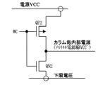
図13には、この発明に係るスタティック型RAMに用いられる電源回路の更に他の一実施例の回路図が示されている。この実施例は、前記図1や図6の実施例のような電源電圧VCC側に電源回路を設ける構成に代えて、選択された相補ビット線に対応したメモリセルの書き込み動作マージンの向上を図りつつ、上記非選択相補ビット線に接続される非選択メモリセルのSNMを確保するために、相補ビット線/BL0,BL0〜/BLm,BLmのそれぞれに対応してメモリセル電源線VSS0〜VSSmを設ける。つまり、同図のメモリセル接地線VSSは、対応する相補ビット/BL0,BL0に接続されるメモリセルの接地線とされる。そして、上記各メモリセル接地線VSS’と回路の接地線VSSとの間には、図13に示したような接地供給回路が設けられる。 FIG. 13 is a circuit diagram showing still another embodiment of the power supply circuit used in the static RAM according to the present invention. In this embodiment, instead of the configuration in which the power supply circuit is provided on the power supply voltage VCC side as in the embodiments of FIGS. 1 and 6, the write operation margin of the memory cell corresponding to the selected complementary bit line is improved. On the other hand, in order to secure the SNM of the non-selected memory cells connected to the non-selected complementary bit lines, the memory cell power supply lines VSS0 to VSSm are set corresponding to the complementary bit lines / BL0, BL0 to / BLm, BLm, respectively. Provide. In other words, the memory cell ground line VSS in the figure is a ground line of the memory cell connected to the corresponding complementary bit / BL0, BL0. A ground supply circuit as shown in FIG. 13 is provided between each of the memory cell ground lines VSS ′ and the circuit ground line VSS.
この実施例では、選択された相補ビット線/BL,BLに対応して書込信号WCBがロウレベルにされる。これにより、NチャネルMOSFETQQN3はオフ状態になり、PチャネルMOSFETQP4がオン状態になる。したがって、選択された相補ビット線/BL,BLに接続された多数のメモリセルに流れるリーク電流や書き込み動作のために流れる電流は上記PチャネルMOSFETQP4を通って流れることとなり、メモリセルの接地電位VSS’をVthだけ上昇させる。つまり、書き込み動作が行われるメモリセルにはVCC−Vthのような低電圧しか与えられないから、前記図9の実施例と等価となり、書き込みマージンを大きくできる。これに対して、非選択の相補ビット線/BL,BLに対応してメモリセルの接地線VSS’は、NチャネルMOSFETQN3がオン状態となっており接地電位VSSがそのまま伝えられる。これにより、上記非選択相補ビット線に接続される非選択メモリセルの動作電圧はVCCとなり前記同様にSNMを確保することができる。 In this embodiment, the write signal WCB is set to the low level corresponding to the selected complementary bit lines / BL, BL. As a result, the N-channel MOSFET QQN3 is turned off and the P-channel MOSFET QP4 is turned on. Therefore, the leakage current flowing through a large number of memory cells connected to the selected complementary bit lines / BL, BL and the current flowing for the write operation flow through the P-channel MOSFET QP4, and the ground potential VSS of the memory cell. Increase 'by Vth. That is, since only a low voltage such as VCC-Vth is applied to the memory cell in which the write operation is performed, this is equivalent to the embodiment of FIG. 9 and the write margin can be increased. On the other hand, the ground potential VSS 'of the memory cell corresponding to the non-selected complementary bit lines / BL, BL is in the on state, and the ground potential VSS is transmitted as it is. As a result, the operating voltage of the non-selected memory cell connected to the non-selected complementary bit line becomes VCC, and the SNM can be secured in the same manner as described above.
この実施例の接地供給回路は、並列形態にされたPチャネルMOSFETQP4とNチャネルMOSFETQN3から構成される。これらのMOSFETQP4とQN3のゲートには、前記図12に示したようなインバータ回路INV1によって反転された書込信号WCBが供給される。この実施例の接地供給回路は、実質的には前記のような電源回路とみなすことができる。つまり、メモリセルは電源電圧VCCと接地電圧VSSとの電圧差が動作電圧として与えられて動作するから、前記実施例のように電源電圧VCCを低下させた電圧VCC’を供給することと、回路の接地電位VSSを上昇させた電圧VSS’を供給することとはメモリセルの動作にとってみれば等価となる。 The ground supply circuit of this embodiment includes a P-channel MOSFET QP4 and an N-channel MOSFET QN3 arranged in parallel. A write signal WCB inverted by the inverter circuit INV1 as shown in FIG. 12 is supplied to the gates of these MOSFETs QP4 and QN3. The ground supply circuit of this embodiment can be regarded substantially as a power supply circuit as described above. That is, since the memory cell operates with a voltage difference between the power supply voltage VCC and the ground voltage VSS as an operating voltage, the memory cell supplies the voltage VCC ′ obtained by reducing the power supply voltage VCC as in the above-described embodiment, and the circuit. Supplying the voltage VSS ′ obtained by increasing the ground potential VSS is equivalent to the operation of the memory cell.
前記図1の実施例のように、ビット線との間での容量結合によって接地線をハイレベル側に持ち上げるようにするためには、ビット線をロウレベルにプリチャージしておいて入力データに対応して一方のビット線を電源電圧VCCのようなハイレベルにディスチャージする構成とすればよい。 As in the embodiment of FIG. 1, in order to raise the ground line to the high level side by capacitive coupling with the bit line, the bit line is precharged to the low level and corresponding to the input data. In this case, one bit line may be discharged to a high level like the power supply voltage VCC.
図14には、この発明に係るメモリセルの他の一実施例のレイアウト図が示されている。図14の(A)及び図14(C)は、前記図4(A)と図4(C)と同様であり、配線層M1〜M4等の記号は省略されている。この実施例では、寄生容量C1とC2の容量値を大きくするための工夫が示されている。電源線VCC’の配線幅を広くしてビット線/BL、BLとの間の間隔を短くしても寄生容量は大きくすることができる。しかし、反面電源線VCC’と他の回路ノード、例えば回路の接地電位等との寄生容量も増大する。この寄生容量は、上記ビット線からのカップリングによる電位変化を阻止する方向に作用するので、効果的なカップリング容量の強化策とはいえない。そこで、この実施例では、電源線VCC’の配線幅を広げることなく、両ビット線/BL,BLとの間隔が等分に短くなるよう蛇行させる。これにより、寄生容量C1とC2を大きくし、しかも電源線VCC’と回路の接地電位等との寄生容量をそのままにできるので、書き込み動作によるビット線電位の変化に対応してメモリセル電圧VCC’の落ち込みを効果的に行わせるようにすることができる。 FIG. 14 is a layout diagram showing another embodiment of the memory cell according to the present invention. 14A and 14C are the same as FIGS. 4A and 4C, and symbols such as the wiring layers M1 to M4 are omitted. In this embodiment, a device for increasing the capacitance values of the parasitic capacitors C1 and C2 is shown. The parasitic capacitance can be increased even if the wiring width of the power supply line VCC ′ is increased and the distance between the bit lines / BL and BL is shortened. However, the parasitic capacitance between the power supply line VCC ′ and other circuit nodes such as the ground potential of the circuit also increases. Since this parasitic capacitance acts in the direction of preventing potential change due to coupling from the bit line, it cannot be said that it is an effective coupling capacitance enhancement measure. In this embodiment, therefore, the power supply line VCC 'is meandered so that the distance between the bit lines / BL and BL is equally reduced without increasing the wiring width. As a result, the parasitic capacitances C1 and C2 can be increased, and the parasitic capacitance between the power supply line VCC ′ and the circuit ground potential can be left as it is. Can be effectively reduced.
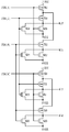
図15には、図1又は図6のスタティック型RAMに用いられるワードドライバの一実施例の回路図が示されている。この実施例では、代表として4つのワード線WL0〜WL3に対応した4個のワードドライバが例示的に示されている。この実施例では、ハイレベルを論理1と正論理を採る場合、ノアゲート(NOR)回路をワードドライバとして用いる。つまり、ワード線WL0に対応したワードドライバを例にして説明すると、電源電圧VDDと出力端子(WL0)との間にPチャネルMOSFETPA0とPB0とが直列形態に接続され、回路の接地電位VSSと出力端子(WL0)との間にNチャネルMOSFETNA0とNB0とが並列形態に接続される。そして、PチャネルMOSFETPA0とNチャネルMOSFETNA0のゲートが共通接続されて入力信号PDA〔0〕が供給され、PチャネルMOSFETPB0とNチャネルMOSFETNB0のゲートが共通接続されて入力信号PDB〔0〕が供給される。
FIG. 15 shows a circuit diagram of an embodiment of a word driver used in the static RAM of FIG. 1 or FIG. In this embodiment, four word drivers corresponding to four word lines WL0 to WL3 are exemplarily shown as representatives. In this embodiment, when the high level is a
上記PチャネルMOSFETPA0のソースに上記電源電圧VCCが供給され、上記PチャネルMOSFETPB0のドレインは出力端子に接続される。この出力端子には上記ワード線WL0が接続される。また、NチャネルMOSFETNA0とNB0のソースには、回路の接地電位VSSが供給され、上記MOSFETNA0とNB0のドレインは、上記出力端子に共通に接続される。 The power supply voltage VCC is supplied to the source of the P-channel MOSFET PA0, and the drain of the P-channel MOSFET PB0 is connected to the output terminal. The word line WL0 is connected to this output terminal. Further, the ground potential VSS of the circuit is supplied to the sources of the N-channel MOSFETs NA0 and NB0, and the drains of the MOSFETs NA0 and NB0 are commonly connected to the output terminal.
この実施例では、特に制限されないが、回路の簡素化のために、PチャネルMOSFETPA0は、ワード線WL1に対応したワードドライバにも共通に用いられる。つまり、ワード線WL1に対応したワードドライバは、上記PチャネルMOSFETPA0とPB1とが直列形態に接続され、回路の接地電位VSSと出力端子(WL1)との間にNチャネルMOSFETNA1とNB1とが並列形態に接続される。そして、PチャネルMOSFETPA0とNチャネルMOSFETNA1のゲートが共通接続されて上記入力信号PDA〔0〕が供給され、PチャネルMOSFETPB1とNチャネルMOSFETNB1のゲートが共通接続されて入力信号PDB〔1〕が供給される。 In this embodiment, although not particularly limited, for simplification of the circuit, the P-channel MOSFET PA0 is also commonly used for a word driver corresponding to the word line WL1. That is, in the word driver corresponding to the word line WL1, the P-channel MOSFETs PA0 and PB1 are connected in series, and the N-channel MOSFETs NA1 and NB1 are connected in parallel between the circuit ground potential VSS and the output terminal (WL1). Connected to. The gates of the P-channel MOSFET PA0 and the N-channel MOSFET NA1 are connected in common and the input signal PDA [0] is supplied. The gates of the P-channel MOSFET PB1 and the N-channel MOSFET NB1 are connected in common and the input signal PDB [1] is supplied. The
残りの2つのワード線WL2と3においても、電源電圧VCCにソースが接続されたPチャネルMOSFETPA2が2つのワードドライバに共通に用いられる。つまり、ワード線WL2に対応したワードドライバでは、前記同様に電源電圧VCCと出力端子(WL2)との間にPチャネルMOSFETPA2とPB2とが直列形態に接続され、回路の接地電位VSSと出力端子(WL2)との間にNチャネルMOSFETNA2とNB2とが並列形態に接続される。そして、PチャネルMOSFETPA2とNチャネルMOSFETNA2のゲートが共通接続されて入力信号PDA〔1〕が供給され、PチャネルMOSFETPB2とNチャネルMOSFETNB2のゲートが共通接続されて入力信号PDB〔0〕が供給される。 In the remaining two word lines WL2 and WL3, a P-channel MOSFET PA2 whose source is connected to the power supply voltage VCC is used in common for the two word drivers. That is, in the word driver corresponding to the word line WL2, the P-channel MOSFETs PA2 and PB2 are connected in series between the power supply voltage VCC and the output terminal (WL2) as described above, and the circuit ground potential VSS and the output terminal ( WL2) and N-channel MOSFETs NA2 and NB2 are connected in parallel. The gates of the P-channel MOSFET PA2 and the N-channel MOSFET NA2 are connected in common and the input signal PDA [1] is supplied. The gates of the P-channel MOSFET PB2 and the N-channel MOSFET NB2 are connected in common and the input signal PDB [0] is supplied. .
上記PチャネルMOSFETPA2は、ワード線WL3に対応したワードドライバにも共通に用いられる。つまり、ワード線WL3に対応したワードドライバは、上記電源電圧VCCと出力端子(WL3)との間に上記PチャネルMOSFETPA2とPB3とが直列形態に接続され、回路の接地電位VSSと出力端子(WL3)との間にNチャネルMOSFETNA3とNB3とが並列形態に接続される。そして、PチャネルMOSFETPA2とNチャネルMOSFETNA3のゲートが共通接続されて上記入力信号PDA〔1〕が供給され、PチャネルMOSFETPB3とNチャネルMOSFETNB3のゲートが共通接続されて入力信号PDB〔1〕が供給される。 The P-channel MOSFET PA2 is also used in common for the word driver corresponding to the word line WL3. That is, in the word driver corresponding to the word line WL3, the P-channel MOSFETs PA2 and PB3 are connected in series between the power supply voltage VCC and the output terminal (WL3), and the circuit ground potential VSS and the output terminal (WL3) are connected. N-channel MOSFETs NA3 and NB3 are connected in parallel. The gates of the P-channel MOSFET PA2 and the N-channel MOSFET NA3 are commonly connected to supply the input signal PDA [1], and the gates of the P-channel MOSFET PB3 and the N-channel MOSFET NB3 are commonly connected to supply the input signal PDB [1]. The
上記入力信号PDA〔0〕と〔1〕は、アクティブ時には相補(排他)関係にある信号であり、一方がハイレベルのときには他方がロウレベルにされる。上記入力信号PDB〔0〕と〔1〕も同様に、アクティブ時には相補(排他)関係にある信号であり、一方がハイレベルのときには他方がロウレベルにされる。特に制限されないが、これらの入力信号入力信号PDAとPDBは、アドレス信号の他に後述するようなクロック信号成分及びスタンバイ信号成分が含まれる。 The input signals PDA [0] and [1] are complementary (exclusive) signals when active, and when one is at a high level, the other is at a low level. Similarly, the input signals PDB [0] and [1] are complementary (exclusive) signals when active, and when one is at a high level, the other is at a low level. Although not particularly limited, these input signal input signals PDA and PDB include a clock signal component and a standby signal component as described later in addition to the address signal.
入力信号PDAは、特に制限されないが、アドレス信号の上位ビット側とされ、入力信号PDBは下位ビット側とされる。したがって、入力信号PDA〔0〕がロウレベルで、入力信号PDA〔1〕がハイレベル、入力信号PDB〔0〕がロウレベルで、入力信号PDB〔1〕がハイレベルのときには、入力信号PDA〔0〕のロウレベルと入力信号PDB〔0〕のロウレベルに対応してPチャネルMOSFETPA0とPB0がオン状態となり、NチャネルMOSFETNA0とNB0がオフ状態となり、ワード線WL0を電源電圧VCCのようなハイレベルの選択状態とされる。他のワード線WL1〜3に対応したワードドライバでは、入力信号PDA〔1〕のハイレベルにより、2つのPチャネルMOSFETのうち少なくともいずれか1つがオフ状態となり、2つのNチャネルMOSFETのうち少なくともいずれか1つがオン状態となり、接地電位VSSのようなロウレベルの非選択状態とされる。 The input signal PDA is not particularly limited, but is on the upper bit side of the address signal, and the input signal PDB is on the lower bit side. Therefore, when the input signal PDA [0] is low level, the input signal PDA [1] is high level, the input signal PDB [0] is low level, and the input signal PDB [1] is high level, the input signal PDA [0] The P channel MOSFETs PA0 and PB0 are turned on in response to the low level of the input signal PDB [0] and the N channel MOSFETs NA0 and NB0 are turned off, and the word line WL0 is selected at a high level like the power supply voltage VCC. It is said. In the word drivers corresponding to the other word lines WL1 to WL3, at least one of the two P-channel MOSFETs is turned off by the high level of the input signal PDA [1], and at least one of the two N-channel MOSFETs. One of them is turned on, and a low level unselected state such as the ground potential VSS is set.
スタンバイ状態では、入力信号PDA〔0〕、〔1〕及び入力信号PDB〔0〕、〔1〕が全てハイレベルにされる。これにより、全てのPチャネルMOSFETはオフ状態にされ、全てのNチャネルMOSFETはオン状態にされる。上記PチャネルMOSFETは、前記のようなリーク電流が流れると、直列MOSFETの接続点の電位がVSSからVCC/2に向かって上昇し、電源電圧側のPチャネルMOSFETPA1,PA2においてソース電位が上昇して、基板との間が逆バイアスとなるというソースバイアス効果によってリーク電流を大幅に低減させることができる。 In the standby state, the input signals PDA [0], [1] and the input signals PDB [0], [1] are all set to the high level. As a result, all P-channel MOSFETs are turned off, and all N-channel MOSFETs are turned on. In the P-channel MOSFET, when a leak current as described above flows, the potential at the connection point of the series MOSFET rises from VSS to VCC / 2, and the source potential rises in the P-channel MOSFETs PA1 and PA2 on the power supply voltage side. Thus, the leak current can be greatly reduced by the source bias effect that the reverse bias is applied to the substrate.
前記のようにワード線WL0が選択状態のとき、それに対応したワードドライバのPチャネルMOSFETPA0、PB0あるいはPA0又はPB0のうち少なくともどちらか一方がオフ状態になる。ワードドライバは、NOR型論理ゲート回路の特徴であるPチャネルMOSFETの縦積みとすることによる,ソースバイアス効果によってリーク電流を小さくできる。特に、入力信号PDA〔0〕〔1〕、PDB〔0〕〔1〕が共にハイレベルになるスタンバイ状態になると、前記のように2つのPチャネルMOSFETが共にオフ状態になり、ソースバイアス効果によってリーク電流が大幅に低減できる。この実施例のように、PチャネルMOSFETPA0,PA2を2つのワードドライバに供給しても、2つのワード線が同時に選択されないために駆動力を維持しながらもリーク削減効果が高まる。デコード論理によっては共有されるワードドライバ数は例えば2のべき乗で増加させることが可能である。 As described above, when the word line WL0 is in the selected state, at least one of the P-channel MOSFETs PA0, PB0 or PA0 or PB0 of the corresponding word driver is turned off. In the word driver, the leakage current can be reduced by the source bias effect by vertically stacking P-channel MOSFETs, which is a feature of the NOR type logic gate circuit. In particular, when the input signals PDA [0] [1] and PDB [0] [1] are both in a standby state in which they are at a high level, the two P-channel MOSFETs are both turned off as described above. Leakage current can be greatly reduced. As in this embodiment, even if the P-channel MOSFETs PA0 and PA2 are supplied to two word drivers, the two word lines are not selected at the same time, so that the leakage reduction effect is enhanced while maintaining the driving force. Depending on the decoding logic, the number of shared word drivers can be increased by a power of 2, for example.
この実施例回路の特徴は、リーク電流を低減させるための特別な制御信号が不要であるという点である。そして、入力信号PDAにクロック信号成分を含ませた場合、つまりはビット線をプリチャージするときに、全ワード線を非選択とする必要がある。このプリチャージ期間の全ワード線非選択状態において、上記のようなソースバイアス効果によるリーク電流を低減させることができる。つまり、スタイバイ状態のみならずメモリアクセス時でのリーク電流も低減させることができるものとなる。 A feature of this embodiment circuit is that a special control signal for reducing the leakage current is not required. When the clock signal component is included in the input signal PDA, that is, when the bit lines are precharged, it is necessary to deselect all the word lines. In all word line non-selected states during this precharge period, the leakage current due to the source bias effect as described above can be reduced. That is, not only the standby state but also the leakage current at the time of memory access can be reduced.
すなわち、LSI(Large Scale Integrated circuit:大規模集積回路) の低消費電力化およびLSI中のトランジスタ(MOSFET)の微細化により、LSIの電源電圧が低下している。たとえば、0.13μmプロセスでは、電源電圧1.2Vで動作するLSIが製造される。LSIの電源電圧を下げる場合には、回路性能(回路の動作速度)を低下させないために、トランジスタのしきい値電圧(Vth)を下げてトランジスタの電流を増加させており、たとえば、0.13μmプロセスでは、Vthが0.4V程度であるMOSFETが使用される。Vthが低いトランジスタでは、サブスレショルド電流と呼ばれるトランジスタがオフ状態の場合にソース・ドレイン間に流れる電流が大きくなる。この電流は、そのトランジスタで構成された回路が動作していない場合にも流れ続け、LSIが通電されているが動作していない状態(以降スタンバイ状態)での消費される電流となる。スタンバイ状態でもデータを記憶しておく必要のあるメモリ回路ではスタンバイ状態でも電源を遮断することができないため、回路を構成するトランジスタのVthが下がるとサブスレッショルド電流が増加しスタンバイ時の消費電力が増加してしまうという問題を上記ワードドライバによって解決できる。 That is, the power supply voltage of the LSI is lowered due to the low power consumption of the LSI (Large Scale Integrated circuit) and the miniaturization of the transistor (MOSFET) in the LSI. For example, in the 0.13 μm process, an LSI that operates with a power supply voltage of 1.2 V is manufactured. When the power supply voltage of the LSI is lowered, the transistor current is increased by lowering the threshold voltage (Vth) of the transistor in order not to lower the circuit performance (circuit operating speed), for example, 0.13 μm. In the process, a MOSFET having a Vth of about 0.4V is used. In a transistor having a low Vth, when a transistor called a subthreshold current is in an off state, a current flowing between the source and the drain increases. This current continues to flow even when a circuit constituted by the transistor is not operating, and becomes a current consumed when the LSI is energized but not operating (hereinafter referred to as a standby state). In a memory circuit that needs to store data even in the standby state, the power cannot be cut off even in the standby state. Therefore, when the Vth of the transistors constituting the circuit decreases, the subthreshold current increases and the power consumption during standby increases. The word driver can solve this problem.
図16には、この発明に係るスタティック型RAMの一実施例の全体回路図が示されている。スタティック型RAMは、メモリセルアレイと、その周辺回路に設けられたアドレス選択回路、読み出し回路及び書き込み回路と、その動作を制御するタイミング生成回路から構成される。 FIG. 16 shows an overall circuit diagram of an embodiment of a static RAM according to the present invention. The static RAM is composed of a memory cell array, an address selection circuit, a read circuit and a write circuit provided in its peripheral circuit, and a timing generation circuit for controlling the operation thereof.
メモリセルアレイとして、1本のワード線WLと、2対の相補ビット線BL,/BLと、その交点に設けられた2つのメモリセルが代表として例示的に示されている。上記メモリセルは、前記同様にPチャネルMOSFETQ1,Q3とNチャネルMOSFETQ2,Q4からなる2つのCMOSインバータ回路の入力と出力とが交差接続されたラッチ回路と、このラッチ回路の一対の入出力ノードとビット線BLと/BLとの間に、NチャネルMOSFETQ5とQ6からなる選択スイッチとから構成される。これらのMOSFETQ5とQ6のゲートは、上記ワード線WLに接続される。 As a memory cell array, one word line WL, two pairs of complementary bit lines BL and / BL, and two memory cells provided at the intersection are representatively shown. Similarly to the above, the memory cell includes a latch circuit in which the inputs and outputs of two CMOS inverter circuits composed of P-channel MOSFETs Q1 and Q3 and N-channel MOSFETs Q2 and Q4 are cross-connected, and a pair of input / output nodes of the latch circuit. A selection switch including N-channel MOSFETs Q5 and Q6 is formed between the bit lines BL and / BL. The gates of these MOSFETs Q5 and Q6 are connected to the word line WL.
特に制限されないが、上記メモリセルアレイは、1つのワード線WLに128個のメモリセルが配置される。それ故、相補ビット線BL,/BLは、128対から構成される。一対のビット線BLと/BLには、256個のメモリセルが配置される。それ故、ワード線WLは、0〜255のような256本から構成される。上記各ビット線BL,/BLには、プリチャージ&イコライズ回路PC/EQが設けられる。プリチャージ回路&イコライズ回路PC/EQは、前記図1と同様に相補ビット線BLと/BLに電源電圧のようなプリチャージ電圧を与えるPチャネルMOSFETと、上記相補ビット線BLと/BLとの間を短絡するPチャネルMOSFETから構成される。また、この実施例では上記相補ビット線BLと/BLと電源端子との間には、ゲートとドレインとが交差接続されたPチャネルMOSFETがプルアップMOSFETとして設けられる。これにより、読み出し時にハイレベル側のビット線の落ち込みが防止される。
Although not particularly limited, the memory cell array has 128 memory cells arranged on one word line WL. Therefore, the complementary bit lines BL and / BL are composed of 128 pairs. 256 memory cells are arranged on the pair of bit lines BL and / BL. Therefore, the word line WL is composed of 256
特に制限されないが、上記128対のビット線は、PチャネルMOSFETからなる読み出し用カラムスイッチにより32対の相補の読み出しデータ線RD,/RDに接続される。1つの読み出しデータ線RD,/RDには、4対のビット線BL,/BLのうちいずれか1つに接続される。上記読み出しデータ線RD,/RDには、センスアンプSAが設けられる。センスアンプSAは、PチャネルMOSFETとNチャネルMOSFETからなる2つのCMOSインバータ回路の入力と出力とが交差接続されてなるCMOSラッチ回路と、このCMOSラッチ回路のNチャネルMOSFETのソースと回路の接地電位に設けられたNチャネルMOSFETから構成される。上記読み出しデータ線RD,/RDが上記のように32対設けられることに対応してセンスアンプSAも全体で32個設けられる。 Although not particularly limited, the 128 pairs of bit lines are connected to 32 pairs of complementary read data lines RD and / RD by a read column switch formed of a P-channel MOSFET. One read data line RD, / RD is connected to any one of four pairs of bit lines BL, / BL. A sense amplifier SA is provided on the read data lines RD, / RD. The sense amplifier SA includes a CMOS latch circuit in which the inputs and outputs of two CMOS inverter circuits each composed of a P-channel MOSFET and an N-channel MOSFET are cross-connected, the source of the N-channel MOSFET of this CMOS latch circuit, and the ground potential of the circuit It is comprised from N channel MOSFET provided in. Corresponding to the 32 pairs of read data lines RD and / RD being provided as described above, 32 sense amplifiers SA are also provided in total.
上記センスアンプSAを活性化させるNチャネルMOSFETのゲート及び上記センスアンプSAの増幅信号を伝えるゲート回路には、タイミング生成回路で形成されたタイミング信号と、センスアンプ選択信号sacを受けるゲート回路で形成されたタイミング制御信号φsacがインバータ回路列を通して伝えられる。このタイミング制御信号φsacは、前記読み出し用カラムスイッチの選択信号としても用いられる。センスアンプSAは、上記選択信号により活性化されて読み出しデータ線RD,/RDの信号を増幅する。 The gate of the N-channel MOSFET for activating the sense amplifier SA and the gate circuit for transmitting the amplified signal of the sense amplifier SA are formed by a gate circuit for receiving the timing signal formed by the timing generation circuit and the sense amplifier selection signal sac. The timing control signal φsac thus transmitted is transmitted through the inverter circuit array. This timing control signal φsac is also used as a selection signal for the read column switch. The sense amplifier SA is activated by the selection signal and amplifies the signals on the read data lines RD and / RD.
上記センスアンプSAの増幅信号は、MOSFETQ17〜Q22により構成されるラッチ回路LTに伝えられ、出力回路OBにより出力信号doutが形成される。ラッチ回路LTは、出力ラッチ制御信号olcに基づいて形成された信号φolcにより制御されるスルーラッチ回路から構成される。出力回路OBは、出力ドライバ制御信号odcに基づいて形成された信号φodcにより制御されるゲート回路と出力インバータ回路から構成される。 The amplified signal of the sense amplifier SA is transmitted to the latch circuit LT constituted by the MOSFETs Q17 to Q22, and the output signal dout is formed by the output circuit OB. Latch circuit LT is formed of a through latch circuit controlled by signal φolc formed based on output latch control signal olc. The output circuit OB includes a gate circuit controlled by a signal φodc formed based on the output driver control signal odc and an output inverter circuit.
この実施例では、特に制限されないが、上記32個のセンスアンプSAを全て活性化して32ビットからなる読み出し信号を出力させる読み出し動作、上記32個のセンスアンプSAうちの16個を活性化して16ビットからなる読み出し信号を出力させる読み出し動作、あるいは上記32個のセンスアンプSAのうちの8個を活性化して8ビットからなる読み出し信号を出力させる読み出し動作が選択的に可能にされる。上記センスアンプ選択信号sacは、上記3種類の読み出し動作に対応してセンスアンプSA等の制御を行うとともに、リードスイッチ制御信号rswcやカラム選択信号selによりPチャネルMOSFETからなる読み出し用カラムスイッチの非選択信号として用いられる。 In this embodiment, although not particularly limited, a read operation in which all the 32 sense amplifiers SA are activated to output a read signal consisting of 32 bits, 16 of the 32 sense amplifiers SA are activated and 16 A read operation for outputting a read signal composed of bits or a read operation for activating eight of the 32 sense amplifiers SA and outputting a read signal composed of 8 bits is selectively made possible. The sense amplifier selection signal sac controls the sense amplifier SA and the like in response to the above three kinds of read operations, and the non-reading of the read column switch composed of a P-channel MOSFET by the read switch control signal rswc and the column selection signal sel. Used as a selection signal.
上記128対のビット線は、NチャネルMOSFETからなる書き込み用カラムスイッチ(WCP)により32対の相補の書き込みデータ線WD,/WDに接続される。1つの書き込みデータ線WD,/WDは、上記カラムスイッチにより4対のビット線BL,/BLのうちいずれか1つに接続される。上記書き込みデータ線WD,/WDには、書き込み信号dinを書き込みデータ線WDに伝えるインバータ回路列(WDP1)と、反転の書き込み信号を形成するインバータ回路(WDP3)及び反転の書き込み信号を書き込みデータ線/WDに伝えるインバータ回路列(WDP2)からなる書き込み回路(ライトアンプ)が設けられる。この書き込み回路も、上記32対の相補の書き込みデータ線WD,/WDに対応して32個から構成される。 The 128 pairs of bit lines are connected to 32 pairs of complementary write data lines WD and / WD by a write column switch (WCP) made of an N-channel MOSFET. One write data line WD, / WD is connected to any one of the four pairs of bit lines BL, / BL by the column switch. For the write data lines WD, / WD, an inverter circuit row (WDP1) for transmitting a write signal din to the write data line WD, an inverter circuit (WDP3) for forming an inverted write signal, and an inverted write signal for the write data line A write circuit (write amplifier) including an inverter circuit train (WDP2) for transmitting to / WD is provided. This write circuit is also composed of 32 pieces corresponding to the 32 pairs of complementary write data lines WD, / WD.
この実施例のSRAMは、特に制限されないが、上記32個のライトアンプで形成された32ビットからなる書き込み信号を有効とする書き込み動作、上記32個のライトアンプのうち16個で形成された16ビットからなる読み出し信号を有効とする書き込み動作、あるいは上記32個のライトアンプのうちの8個で形成された8ビットからなる書き込み信号を有効とする書き込み動作のいずれかが選択的に可能にされる。このため、ライトスイッチ制御信号wswcが用いられる。この実施例では、上記カラム選択信号がライトスイッチ制御信号wswcと組み合わされてNチャネルMOSFETからなる書き込み用カラムスイッチに伝えられる。 The SRAM of this embodiment is not particularly limited, but a write operation that validates a 32-bit write signal formed by the 32 write amplifiers, and 16 of the 32 write amplifiers are formed by 16 units. Either a write operation for validating a read signal consisting of bits or a write operation for validating a write signal consisting of 8 bits formed by 8 of the 32 write amplifiers can be selectively made possible. The For this reason, the light switch control signal wswc is used. In this embodiment, the column selection signal is combined with the write switch control signal wswc and transmitted to the write column switch composed of an N-channel MOSFET.
上記センスアンプSAの増幅信号は、ゲート回路を通してMOSFETQ17〜Q22と、インバータ回路からなるラッチ回路に伝えられ、ゲート回路及び出力インバータ回路を通して出力信号doutが形成される。上記センスアンプSAを活性化させるNチャネルMOSFETのゲート及び上記センスアンプSAの増幅信号を伝えるゲート回路には、タイミング生成回路で形成されたタイミング信号と、センスアンプ選択信号sacを受けるゲート回路で形成されたタイミング制御信号φsacが制御パスを構成するインバータ回路列を通して伝えられる。このタイミング制御信号φsacは、前記読み出し用カラムスイッチの非選択信号としても用いられる。 The amplified signal of the sense amplifier SA is transmitted to MOSFETs Q17 to Q22 and a latch circuit including an inverter circuit through a gate circuit, and an output signal dout is formed through the gate circuit and the output inverter circuit. The gate of the N-channel MOSFET for activating the sense amplifier SA and the gate circuit for transmitting the amplified signal of the sense amplifier SA are formed by a gate circuit for receiving the timing signal formed by the timing generation circuit and the sense amplifier selection signal sac. The timing control signal φsac thus transmitted is transmitted through an inverter circuit array constituting a control path. This timing control signal φsac is also used as a non-selection signal for the read column switch.
タイミング生成回路は、クロックCLKとリード/ライト制御信号R/Wを代表とするような複数の制御信号を受けて、SRAMの読み出し動作、書き込み動作あるいはスタンバイ動作等の動作モードに対応して、SRAMの動作に必要な各種のタイミング信号を生成する。 The timing generation circuit receives a plurality of control signals such as a clock CLK and a read / write control signal R / W, and corresponds to an operation mode such as a read operation, a write operation, or a standby operation of the SRAM. Various timing signals necessary for the operation are generated.
上記256本からなるワード線WLのうちの1本が、前記説明したようなプリデコーダ回路及びワードドライバ(NOR)によって選択される。プリデコーダ回路は、タイミング生成回路で形成されたタイミング信号(クロック,イネーブル)とアドレス信号addを受けて、上記ワード線を選択するプリデコード信号やカラムの選択信号を形成する。そして、上記スタンバイ動作等の動作モードでは、アドレス信号addに無関係に全てのワード線は非選択レベルにされる。プリデコーダ回路で形成されたカラム選択信号は、図示しない論理回路により、前記32ビット動作、16ビット動作及び8ビット動作に対応して前記制御信号sac,rswc,wswc等を形成するために用いられる。 One of the 256 word lines WL is selected by the predecoder circuit and the word driver (NOR) as described above. The predecoder circuit receives the timing signal (clock, enable) and address signal add generated by the timing generation circuit, and forms a predecode signal for selecting the word line and a column selection signal. In the operation mode such as the standby operation, all the word lines are set to the non-selected level regardless of the address signal add. The column selection signal formed by the predecoder circuit is used to form the control signals sac, rswc, wswc, etc. corresponding to the 32-bit operation, 16-bit operation, and 8-bit operation by a logic circuit (not shown). .
以上本発明者よりなされた発明を実施例に基づき具体的に説明したが、本願発明は前記実施例に限定されるものではなく、その要旨を逸脱しない範囲で種々変更可能であることはいうまでもない。例えば、半導体集積回路装置に搭載されるSRAMのメモリセルアレイを構成するワード線やビット線の本数は、種々の実施形態を採ることができる。SRAMは、システムLSIに混載されるSRAMの他に、汎用メモリとしてのSRAMにも同様に適用することができる。この発明は、前記のようなSRAMを含む半導体集積回路装置に広く利用することができる。 The invention made by the inventor has been specifically described based on the embodiments. However, the invention of the present application is not limited to the embodiments, and various modifications can be made without departing from the scope of the invention. Nor. For example, various embodiments can be adopted for the number of word lines and bit lines constituting an SRAM memory cell array mounted in a semiconductor integrated circuit device. The SRAM can be similarly applied to an SRAM as a general-purpose memory in addition to the SRAM embedded in the system LSI. The present invention can be widely used for semiconductor integrated circuit devices including the SRAM as described above.
QP1〜QP4…PチャネルMOSFET、QN1〜QN3…NチャネルMOSFET、INV1…インバータ回路、R…抵抗、C1,C2…寄生容量(カップリング容量)
NA0〜NA3,N10,N11…NチャネルMOSFET、PA0,PA2、PB0〜PB3…PチャネルMOSFET、WL0〜WL3…ワード線、
WDP1〜WDP3…ライトデータ入力パス(ライトアンプ)、WCP…ライト系制御パス、LT…ラッチ回路、OB…出力回路、SA…センスアンプ、PC/EQ…プリチャージ&イコライズ回路、Q1〜Q6…MOSFET、BL,/BL…ビット線、RD,/RD…読み出しデータ線、WD,/WD…書き込みデータ線。
QP1 to QP4... P channel MOSFET, QN1 to QN3... N channel MOSFET, INV1... Inverter circuit, R... Resistance, C1, C2.
NA0 to NA3, N10, N11... N channel MOSFET, PA0, PA2, PB0 to PB3... P channel MOSFET, WL0 to WL3.
WDP1 to WDP3 ... write data input path (write amplifier), WCP ... write system control path, LT ... latch circuit, OB ... output circuit, SA ... sense amplifier, PC / EQ ... precharge & equalize circuit, Q1 to Q6 ... MOSFET , BL, / BL ... bit lines, RD, / RD ... read data lines, WD, / WD ... write data lines.
Claims (4)
複数の相補ビット線と、
上記複数のワード線と複数の相補ビット線に対応して設けられた複数のスタティック型メモリセルと、
上記複数の相補ビット線のそれぞれに接続される複数からなるメモリセル毎に動作電圧を供給する複数のメモリセル電源線と、
上記複数のメモリセル電源線にそれぞれ電源電圧を供給する複数の電源供給回路とを含み、
上記電源供給回路は、書き込み制御信号と対応する相補ビット線の選択信号に基づいて形成された制御信号によってメモリセルへの書き込み時にオフ状態にされる第1PチャネルMOSFETからなるスタティック型RAMを備え、
上記電源電圧は、正の電圧であり、
上記メモリセル電源線と回路の接地電位との間には、上記第1PチャネルMOSFETと相補的にスイッチ制御されてなる第2PチャネルMOSFETを更に備えてなることを特徴とする半導体集積回路装置。 Multiple word lines,
A plurality of complementary bit lines;
A plurality of static memory cells provided corresponding to the plurality of word lines and the plurality of complementary bit lines;
A plurality of memory cell power supply lines for supplying an operating voltage to each of the plurality of memory cells connected to each of the plurality of complementary bit lines;
A plurality of power supply circuits for supplying a power supply voltage to each of the plurality of memory cell power lines,
The power supply circuit includes a static RAM including a first P-channel MOSFET that is turned off when writing to the memory cell by a control signal formed based on a selection signal of a complementary bit line corresponding to the write control signal,
The power supply voltage is a positive voltage,
Between the ground potential of the upper Symbol memory cell power supply line and the circuit, the semiconductor integrated circuit device characterized by comprising further comprising a second 2P-channel MOSFET formed by complementarily switching control between the first 1P channel MOSFET.
上記メモリセルは、2つのCMOSインバータ回路の入力と出力が交差接続されている記憶部と、かかる記憶部と上記相補ビット線との間に設けられ、ゲートが上記ワード線に接続された選択MOSFETからなることを特徴とする半導体集積回路装置。 In claim 1 ,
The memory cell includes a storage section in which inputs and outputs of two CMOS inverter circuits are cross-connected, and a selection MOSFET provided between the storage section and the complementary bit line, and having a gate connected to the word line A semiconductor integrated circuit device comprising:
上記相補ビット線には、上記電源電圧に対応したプリチャージ電圧を供給するプリチャージ回路が設けられ、
上記メモリセル電源線は、対応する相補ビット線との間で寄生容量を持つようにされてなることを特徴とする半導体集積回路装置。 In claim 1 ,
The complementary bit line is provided with a precharge circuit for supplying a precharge voltage corresponding to the power supply voltage,
The semiconductor integrated circuit device, wherein the memory cell power supply line has a parasitic capacitance with a corresponding complementary bit line.
上記複数のワード線のうちの1つを選択するワード線選択回路を更に備え、
上記ワード線選択回路は、
上記電源電圧と出力端子との間に直列形態に接続されたPチャネル型の第1、第2MOSFETと、
回路の接地電位と上記出力端子との間に並列形態に接続されたNチャネル型の第3、第4MOSFETとを備え、
上記第1MOSFETと第3MOSFETのゲートには第1信号が供給され、
上記第2MOSFETと第4MOSFETのゲートには第2信号が供給され、
上記出力端子は、上記複数のワード線のうち対応する1つに接続され、
上記ワード線選択時に上記第1信号と第2信号に対応して上記第1及び第2MOSFETがオン状態となり、上記第3及び第4MOSFETがオフ状態となって上記出力端子を第1電圧に対応した選択レベルにするワードドライバを備えてなることを特徴とする半導体集積回路装置。 In claim 1 ,
A word line selection circuit for selecting one of the plurality of word lines;
The word line selection circuit is
P-channel type first and second MOSFETs connected in series between the power supply voltage and the output terminal;
N-channel third and fourth MOSFETs connected in parallel between the circuit ground potential and the output terminal,
A first signal is supplied to the gates of the first MOSFET and the third MOSFET,
A second signal is supplied to the gates of the second MOSFET and the fourth MOSFET,
The output terminal is connected to a corresponding one of the plurality of word lines,
When the word line is selected, the first and second MOSFETs are turned on corresponding to the first signal and the second signal, the third and fourth MOSFETs are turned off, and the output terminal corresponds to the first voltage. A semiconductor integrated circuit device comprising a word driver for selecting a level.
Priority Applications (15)
| Application Number | Priority Date | Filing Date | Title |
|---|---|---|---|
| JP2004267645A JP4553185B2 (en) | 2004-09-15 | 2004-09-15 | Semiconductor integrated circuit device |
| US11/127,286 US7113421B2 (en) | 2004-09-15 | 2005-05-12 | Semiconductor integrated circuit device |
| TW94115789A TWI397070B (en) | 2004-09-15 | 2005-05-16 | Semiconductor integnated circuit device |
| TW101147444A TWI576838B (en) | 2004-09-15 | 2005-05-16 | Semiconductor integrated circuit device |
| TW105102684A TW201619961A (en) | 2004-09-15 | 2005-05-16 | Semiconductor integrated circuit device |
| CN2005100791297A CN1750171B (en) | 2004-09-15 | 2005-06-24 | Semiconductor integrated circuit device |
| CN2010101667777A CN101866686B (en) | 2004-09-15 | 2005-06-24 | Semiconductor integrated circuite device |
| KR20050066535A KR101168340B1 (en) | 2004-09-15 | 2005-07-22 | Semiconductor integrated circuit device |
| US11/504,079 US7477537B2 (en) | 2004-09-15 | 2006-08-15 | Semiconductor integrated circuit device |
| US11/504,077 US7420834B2 (en) | 2004-09-15 | 2006-08-15 | Semiconductor integrated circuit device |
| US12/314,190 US7715223B2 (en) | 2004-09-15 | 2008-12-05 | Semiconductor integrated circuit device |
| US12/662,029 US8072799B2 (en) | 2004-09-15 | 2010-03-29 | Semiconductor integrated circuit device |
| US13/317,846 US8441843B2 (en) | 2004-09-15 | 2011-10-31 | Semiconductor integrated circuit device |
| US13/874,834 US9123435B2 (en) | 2004-09-15 | 2013-05-01 | Semiconductor integrated circuit device |
| US14/835,127 US20150380076A1 (en) | 2004-09-15 | 2015-08-25 | Semiconductor integrated circuit device |
Applications Claiming Priority (1)
| Application Number | Priority Date | Filing Date | Title |
|---|---|---|---|
| JP2004267645A JP4553185B2 (en) | 2004-09-15 | 2004-09-15 | Semiconductor integrated circuit device |
Related Child Applications (1)
| Application Number | Title | Priority Date | Filing Date |
|---|---|---|---|
| JP2010112712A Division JP5456571B2 (en) | 2010-05-15 | 2010-05-15 | Semiconductor integrated circuit device |
Publications (3)
| Publication Number | Publication Date |
|---|---|
| JP2006085786A JP2006085786A (en) | 2006-03-30 |
| JP2006085786A5 JP2006085786A5 (en) | 2007-10-18 |
| JP4553185B2 true JP4553185B2 (en) | 2010-09-29 |
Family
ID=36033731
Family Applications (1)
| Application Number | Title | Priority Date | Filing Date |
|---|---|---|---|
| JP2004267645A Active JP4553185B2 (en) | 2004-09-15 | 2004-09-15 | Semiconductor integrated circuit device |
Country Status (5)
| Country | Link |
|---|---|
| US (8) | US7113421B2 (en) |
| JP (1) | JP4553185B2 (en) |
| KR (1) | KR101168340B1 (en) |
| CN (2) | CN101866686B (en) |
| TW (3) | TWI397070B (en) |
Cited By (1)
| Publication number | Priority date | Publication date | Assignee | Title |
|---|---|---|---|---|
| US9990986B1 (en) | 2016-12-06 | 2018-06-05 | Samsung Electronics Co., Ltd. | Static random access memory device having uniform write characteristics |
Families Citing this family (101)
| Publication number | Priority date | Publication date | Assignee | Title |
|---|---|---|---|---|
| US7167025B1 (en) | 2004-02-14 | 2007-01-23 | Herman Schmit | Non-sequentially configurable IC |
| US7425841B2 (en) | 2004-02-14 | 2008-09-16 | Tabula Inc. | Configurable circuits, IC's, and systems |
| JP4553185B2 (en) * | 2004-09-15 | 2010-09-29 | ルネサスエレクトロニクス株式会社 | Semiconductor integrated circuit device |
| US7317331B2 (en) | 2004-11-08 | 2008-01-08 | Tabula, Inc. | Reconfigurable IC that has sections running at different reconfiguration rates |
| US7330050B2 (en) | 2004-11-08 | 2008-02-12 | Tabula, Inc. | Storage elements for a configurable IC and method and apparatus for accessing data stored in the storage elements |
| US7236009B1 (en) | 2004-12-01 | 2007-06-26 | Andre Rohe | Operational time extension |
| US7230869B1 (en) * | 2005-03-15 | 2007-06-12 | Jason Redgrave | Method and apparatus for accessing contents of memory cells |
| US7272031B1 (en) * | 2005-03-15 | 2007-09-18 | Tabula, Inc. | Method and apparatus for reduced power cell |
| JP4912016B2 (en) | 2005-05-23 | 2012-04-04 | ルネサスエレクトロニクス株式会社 | Semiconductor memory device |
| JP5100035B2 (en) | 2005-08-02 | 2012-12-19 | ルネサスエレクトロニクス株式会社 | Semiconductor memory device |
| US7372297B1 (en) | 2005-11-07 | 2008-05-13 | Tabula Inc. | Hybrid interconnect/logic circuits enabling efficient replication of a function in several sub-cycles to save logic and routing resources |
| TWI266338B (en) * | 2005-12-01 | 2006-11-11 | Via Tech Inc | Output circuit of SRAM |
| US7679401B1 (en) | 2005-12-01 | 2010-03-16 | Tabula, Inc. | User registers implemented with routing circuits in a configurable IC |
| JP2007172715A (en) * | 2005-12-20 | 2007-07-05 | Fujitsu Ltd | Semiconductor memory device and its control method |
| US7669097B1 (en) | 2006-03-27 | 2010-02-23 | Tabula, Inc. | Configurable IC with error detection and correction circuitry |
| US7292495B1 (en) * | 2006-06-29 | 2007-11-06 | Freescale Semiconductor, Inc. | Integrated circuit having a memory with low voltage read/write operation |
| US7793172B2 (en) * | 2006-09-28 | 2010-09-07 | Freescale Semiconductor, Inc. | Controlled reliability in an integrated circuit |
| US7492627B2 (en) * | 2006-11-17 | 2009-02-17 | Freescale Semiconductor, Inc. | Memory with increased write margin bitcells |
| JP2008227171A (en) * | 2007-03-13 | 2008-09-25 | Toshiba Corp | Nonvolatile semiconductor memory |
| US7521959B2 (en) | 2007-03-20 | 2009-04-21 | Tabula, Inc. | Configurable IC having a routing fabric with storage elements |
| US7535252B1 (en) | 2007-03-22 | 2009-05-19 | Tabula, Inc. | Configurable ICs that conditionally transition through configuration data sets |
| US7825685B2 (en) | 2007-09-06 | 2010-11-02 | Tabula, Inc. | Configuration context switcher with a clocked storage element |
| JP2009070474A (en) | 2007-09-13 | 2009-04-02 | Panasonic Corp | Semiconductor integrated circuit |
| US7688656B2 (en) * | 2007-10-22 | 2010-03-30 | Freescale Semiconductor, Inc. | Integrated circuit memory having dynamically adjustable read margin and method therefor |
| US7613052B2 (en) * | 2007-11-01 | 2009-11-03 | Arm Limited | Memory device and method of operating such a memory device |
| US8863067B1 (en) | 2008-02-06 | 2014-10-14 | Tabula, Inc. | Sequential delay analysis by placement engines |
| US7643357B2 (en) * | 2008-02-18 | 2010-01-05 | International Business Machines Corporation | System and method for integrating dynamic leakage reduction with write-assisted SRAM architecture |
| JP2009289784A (en) * | 2008-05-27 | 2009-12-10 | Nec Electronics Corp | Semiconductor integrated circuit device |
| JP2009289308A (en) * | 2008-05-28 | 2009-12-10 | Toshiba Corp | Semiconductor memory device |
| US8166435B2 (en) * | 2008-06-26 | 2012-04-24 | Tabula, Inc. | Timing operations in an IC with configurable circuits |
| US8164969B2 (en) * | 2008-07-01 | 2012-04-24 | Jeng-Jye Shau | Ultra-low power hybrid circuits |
| US7782655B2 (en) * | 2008-07-01 | 2010-08-24 | Jeng-Jye Shau | Ultra-low power hybrid sub-threshold circuits |
| CN102105941A (en) * | 2008-08-01 | 2011-06-22 | 松下电器产业株式会社 | Semiconductor memory device |
| JP5197241B2 (en) * | 2008-09-01 | 2013-05-15 | ルネサスエレクトロニクス株式会社 | Semiconductor device |
| US8243541B2 (en) * | 2008-12-19 | 2012-08-14 | Oracle America, Inc. | Methods and apparatuses for improving reduced power operations in embedded memory arrays |
| US8045402B2 (en) * | 2009-06-29 | 2011-10-25 | Arm Limited | Assisting write operations to data storage cells |
| JP4857367B2 (en) * | 2009-07-06 | 2012-01-18 | 株式会社沖データ | Drive circuit and image forming apparatus |
| JP5317900B2 (en) | 2009-09-14 | 2013-10-16 | ルネサスエレクトロニクス株式会社 | Semiconductor integrated circuit and operation method thereof |
| KR101034616B1 (en) * | 2009-11-30 | 2011-05-12 | 주식회사 하이닉스반도체 | Sense amplifier and semiconductor memory device |
| JP5596335B2 (en) * | 2009-12-24 | 2014-09-24 | ルネサスエレクトロニクス株式会社 | Semiconductor device |
| KR20220145923A (en) * | 2009-12-25 | 2022-10-31 | 가부시키가이샤 한도오따이 에네루기 켄큐쇼 | Memory device, semiconductor device, and electronic device |
| JP5380332B2 (en) | 2010-03-02 | 2014-01-08 | ルネサスエレクトロニクス株式会社 | Semiconductor device and data processor |
| US8218376B2 (en) * | 2010-04-21 | 2012-07-10 | Texas Instruments Incorporated | Reduced power consumption in retain-till-accessed static memories |
| US20120008419A1 (en) * | 2010-07-09 | 2012-01-12 | Ha Joo Yun | Semiconductor memory device and method of operating the same |
| KR101192583B1 (en) | 2010-10-28 | 2012-10-18 | 삼성디스플레이 주식회사 | Liquid crystal display panel, liquid crystal display device and method of driving a liquid crystal display device |
| US8451652B2 (en) * | 2010-12-02 | 2013-05-28 | Lsi Corporation | Write assist static random access memory cell |
| US8867278B2 (en) * | 2011-02-28 | 2014-10-21 | Samsung Electronics Co., Ltd. | Nonvolatile memory device, memory system including the same, and method of operating nonvolatile memory device |
| CN102290099B (en) * | 2011-07-04 | 2016-04-06 | 上海华虹宏力半导体制造有限公司 | Sram memory and forming method thereof |
| JP5932257B2 (en) * | 2011-07-14 | 2016-06-08 | エスアイアイ・セミコンダクタ株式会社 | Memory circuit |
| JP5705053B2 (en) | 2011-07-26 | 2015-04-22 | ルネサスエレクトロニクス株式会社 | Semiconductor device |
| JP5777991B2 (en) * | 2011-09-22 | 2015-09-16 | ルネサスエレクトロニクス株式会社 | Semiconductor device |
| JP6099368B2 (en) | 2011-11-25 | 2017-03-22 | 株式会社半導体エネルギー研究所 | Storage device |
| WO2013084385A1 (en) | 2011-12-08 | 2013-06-13 | パナソニック株式会社 | Semiconductor storage device |
| US8934314B2 (en) * | 2011-12-28 | 2015-01-13 | Intel Corporation | Apparatus and method for improving power delivery in a memory, such as, a random access memory |
| JP5867091B2 (en) * | 2012-01-10 | 2016-02-24 | 株式会社ソシオネクスト | Semiconductor memory device and writing method thereof |
| US8559251B2 (en) * | 2012-01-20 | 2013-10-15 | Taiwan Semiconductor Manufacturing Company, Ltd. | Memory circuit and method of writing datum to memory circuit |
| KR102296696B1 (en) | 2012-01-23 | 2021-09-02 | 가부시키가이샤 한도오따이 에네루기 켄큐쇼 | Semiconductor device |
| JP5465266B2 (en) * | 2012-02-21 | 2014-04-09 | ルネサスエレクトロニクス株式会社 | Semiconductor memory device |
| US8654594B2 (en) | 2012-02-23 | 2014-02-18 | International Business Machines Corporation | Vdiff max limiter in SRAMs for improved yield and power |
| CN102568564B (en) * | 2012-02-29 | 2014-03-12 | 福州大学 | Combined SET (Single-Electron Transistor)/CMOS (Complementary Metal-Oxide Semiconductor) static storage unit based on NDR (Negative Differential Resistance) property |
| GB2500907B (en) * | 2012-04-04 | 2016-05-25 | Platipus Ltd | Static random access memory devices |
| JP5962185B2 (en) * | 2012-04-27 | 2016-08-03 | 株式会社ソシオネクスト | Semiconductor memory device and control method thereof |
| US8837205B2 (en) * | 2012-05-30 | 2014-09-16 | Freescale Semiconductor, Inc. | Multi-port register file with multiplexed data |
| US9153304B2 (en) * | 2012-06-28 | 2015-10-06 | Jaydeep P. Kulkarni | Apparatus for reducing write minimum supply voltage for memory |
| CN102723110B (en) * | 2012-07-12 | 2015-06-24 | 苏州兆芯半导体科技有限公司 | Write margin control circuit |
| JP5784558B2 (en) * | 2012-08-14 | 2015-09-24 | 株式会社東芝 | Semiconductor memory device |
| US9218881B2 (en) * | 2012-10-23 | 2015-12-22 | Sandisk Technologies Inc. | Flash memory blocks with extended data retention |
| US8953401B2 (en) | 2012-12-07 | 2015-02-10 | United Microelectronics Corp. | Memory device and method for driving memory array thereof |
| KR20140146481A (en) * | 2013-06-17 | 2014-12-26 | 에스케이하이닉스 주식회사 | Column decoder |
| US9105355B2 (en) * | 2013-07-04 | 2015-08-11 | United Microelectronics Corporation | Memory cell array operated with multiple operation voltage |
| TWI562163B (en) * | 2013-07-04 | 2016-12-11 | United Microelectronics Corp | Memory cell array |
| JP6034764B2 (en) | 2013-08-05 | 2016-11-30 | ルネサスエレクトロニクス株式会社 | Semiconductor memory device |
| US9515076B2 (en) * | 2013-08-06 | 2016-12-06 | Renesas Electronics Corporation | Semiconductor integrated circuit device |
| CN104851453B (en) * | 2014-02-18 | 2018-05-18 | 辉达公司 | For the write-in subplan of low power SRAM |
| JP6353668B2 (en) | 2014-03-03 | 2018-07-04 | ルネサスエレクトロニクス株式会社 | Semiconductor memory device |
| US9916874B2 (en) | 2014-08-15 | 2018-03-13 | Taiwan Semiconductor Manufacturing Company, Ltd. | Memory architecture having first and second voltages |
| JP5917738B2 (en) * | 2015-02-24 | 2016-05-18 | ルネサスエレクトロニクス株式会社 | Semiconductor device and semiconductor chip |
| KR20170027493A (en) * | 2015-09-02 | 2017-03-10 | 에스케이하이닉스 주식회사 | layout of semiconductor device |
| US9997235B2 (en) | 2015-12-17 | 2018-06-12 | Taiwan Semiconductor Manufacturing Co., Ltd. | Semiconductor memory with respective power voltages for plurality of memory cells |
| US9865605B2 (en) | 2016-01-14 | 2018-01-09 | Taiwan Semiconductor Manufacturing Company, Ltd. | Memory circuit having resistive device coupled with supply voltage line |
| KR102493815B1 (en) * | 2016-01-29 | 2023-02-01 | 삼성전자주식회사 | Semiconductor device configured to selectively perform isolation function and layout method thereof |
| US10199092B2 (en) * | 2016-06-21 | 2019-02-05 | Arm Limited | Boost circuit for memory |
| US9922701B2 (en) * | 2016-08-08 | 2018-03-20 | Taiwan Semiconductor Manufacturing Company Limited | Pre-charging bit lines through charge-sharing |
| KR102646847B1 (en) * | 2016-12-07 | 2024-03-12 | 삼성전자주식회사 | Semiconductor memory devices, methods of operating semiconductor memory devices and memory systems |
| JP2018206452A (en) * | 2017-05-30 | 2018-12-27 | ルネサスエレクトロニクス株式会社 | Content reference memory and semiconductor device |
| JP2019046514A (en) * | 2017-08-29 | 2019-03-22 | 東芝メモリ株式会社 | Semiconductor storage device |
| CN110097907B (en) * | 2018-01-29 | 2021-03-19 | 展讯通信(上海)有限公司 | SRAM memory |
| JP2018142397A (en) * | 2018-06-20 | 2018-09-13 | ルネサスエレクトロニクス株式会社 | Semiconductor device |
| CN110867201B (en) * | 2018-08-27 | 2022-03-25 | 龙芯中科技术股份有限公司 | Memory cell and multi-port static random access memory |
| CN109584928B (en) * | 2018-11-30 | 2021-07-23 | 中国科学院微电子研究所 | Write assist circuit and write assist method for static random access memory |
| JP7196040B2 (en) * | 2019-03-14 | 2022-12-26 | 株式会社東芝 | semiconductor storage device |
| US11094368B2 (en) | 2019-08-15 | 2021-08-17 | Powerchip Semiconductor Manufacturing Corporation | Memory, memory chip and memory data access method |
| CN110503995A (en) * | 2019-08-19 | 2019-11-26 | 上海华力微电子有限公司 | A kind of read-write optimization circuit for SRAM |
| US11183234B2 (en) * | 2019-11-25 | 2021-11-23 | Taiwan Semiconductor Manufacturing Company, Ltd. | Bitcell supporting bit-write-mask function |
| CN111161785A (en) * | 2019-12-31 | 2020-05-15 | 展讯通信(上海)有限公司 | Static random access memory and fault detection circuit thereof |
| CN112102863B (en) * | 2020-09-07 | 2023-04-25 | 海光信息技术股份有限公司 | Static random access memory control circuit, method, memory and processor |
| CN112382326B (en) * | 2020-12-11 | 2023-11-17 | 北京中科芯蕊科技有限公司 | Sub-threshold dual-power SRAM read auxiliary circuit |
| JP7453135B2 (en) | 2020-12-22 | 2024-03-19 | ルネサスエレクトロニクス株式会社 | semiconductor equipment |
| JP2023016551A (en) * | 2021-07-21 | 2023-02-02 | ルネサスエレクトロニクス株式会社 | Semiconductor device and semiconductor system |
| TWI781836B (en) * | 2021-11-30 | 2022-10-21 | 修平學校財團法人修平科技大學 | Semiconductor memory device |
| TWI781854B (en) * | 2021-12-16 | 2022-10-21 | 修平學校財團法人修平科技大學 | Memory device |
Citations (7)
| Publication number | Priority date | Publication date | Assignee | Title |
|---|---|---|---|---|
| JPS5564686A (en) * | 1978-11-08 | 1980-05-15 | Nec Corp | Memory unit |
| JPH06236688A (en) * | 1992-09-28 | 1994-08-23 | Texas Instr Inc <Ti> | Gate array |
| JPH0863972A (en) * | 1994-08-18 | 1996-03-08 | Kawasaki Steel Corp | Semiconductor storage device |
| JPH10106268A (en) * | 1996-09-30 | 1998-04-24 | Nec Corp | Semiconductor memory |
| JP2001035939A (en) * | 1999-07-16 | 2001-02-09 | Nec Corp | Semiconductor memory device |
| JP2002042476A (en) * | 2000-07-25 | 2002-02-08 | Mitsubishi Electric Corp | Static semiconductor memory |
| JP2003022677A (en) * | 2001-06-29 | 2003-01-24 | Internatl Business Mach Corp <Ibm> | Method and apparatus for writing operation in sram cell |
Family Cites Families (42)
| Publication number | Priority date | Publication date | Assignee | Title |
|---|---|---|---|---|
| US4202146A (en) * | 1979-03-01 | 1980-05-13 | Adams William C | Transportable module for trilevel dwelling |
| US4288865A (en) * | 1980-02-06 | 1981-09-08 | Mostek Corporation | Low-power battery backup circuit for semiconductor memory |
| JPS6038796A (en) | 1983-08-12 | 1985-02-28 | Hitachi Ltd | Semiconductor integrated circuit device |
| US4685087A (en) * | 1983-08-31 | 1987-08-04 | Texas Instruments Incorporated | SRAM with constant pulse width |
| US5159571A (en) * | 1987-12-29 | 1992-10-27 | Hitachi, Ltd. | Semiconductor memory with a circuit for testing characteristics of flip-flops including selectively applied power supply voltages |
| JPH01294295A (en) * | 1988-05-20 | 1989-11-28 | Fujitsu Ltd | Partial random access memory |
| GB2222461B (en) * | 1988-08-30 | 1993-05-19 | Mitsubishi Electric Corp | On chip testing of semiconductor memory devices |
| JPH02108297A (en) | 1988-10-18 | 1990-04-20 | Nippon Telegr & Teleph Corp <Ntt> | Memory cell circuit |
| JP2927463B2 (en) * | 1989-09-28 | 1999-07-28 | 株式会社日立製作所 | Semiconductor storage device |
| US5301147A (en) * | 1993-01-08 | 1994-04-05 | Aptix Corporation | Static random access memory cell with single logic-high voltage level bit-line and address-line drivers |
| JP3354231B2 (en) * | 1993-09-29 | 2002-12-09 | 三菱電機エンジニアリング株式会社 | Semiconductor device |
| JP3015652B2 (en) * | 1994-03-03 | 2000-03-06 | 株式会社東芝 | Semiconductor memory device |
| JP3523718B2 (en) * | 1995-02-06 | 2004-04-26 | 株式会社ルネサステクノロジ | Semiconductor device |
| US5535172A (en) * | 1995-02-28 | 1996-07-09 | Alliance Semiconductor Corporation | Dual-port random access memory having reduced architecture |
| JP4198201B2 (en) * | 1995-06-02 | 2008-12-17 | 株式会社ルネサステクノロジ | Semiconductor device |
| JPH09120682A (en) * | 1995-10-24 | 1997-05-06 | Mitsubishi Electric Corp | Semiconductor memory apparatus |
| JPH09147564A (en) | 1995-11-17 | 1997-06-06 | Nippon Telegr & Teleph Corp <Ntt> | Memory cell array |
| JP3523762B2 (en) * | 1996-12-19 | 2004-04-26 | 株式会社東芝 | Semiconductor storage device |
| TW459389B (en) * | 1997-11-22 | 2001-10-11 | United Microelectronics Corp | Manufacture method of SRAM |
| JP3110407B2 (en) | 1998-12-11 | 2000-11-20 | 日本電気アイシーマイコンシステム株式会社 | Semiconductor storage device |
| JP4565700B2 (en) * | 1999-05-12 | 2010-10-20 | ルネサスエレクトロニクス株式会社 | Semiconductor device |
| KR20020001093A (en) * | 2000-06-24 | 2002-01-09 | 이원창 | one-touch type brake releasing system for train using an air pressure |
| US6529400B1 (en) * | 2000-12-15 | 2003-03-04 | Lsi Logic Corporation | Source pulsed, dynamic threshold complementary metal oxide semiconductor static RAM cells |
| JP4782937B2 (en) * | 2001-03-27 | 2011-09-28 | 株式会社東芝 | Semiconductor memory device |
| JP3910078B2 (en) * | 2001-05-11 | 2007-04-25 | 株式会社ルネサステクノロジ | Semiconductor memory device and method for testing semiconductor memory device |
| JP4895439B2 (en) | 2001-06-28 | 2012-03-14 | ルネサスエレクトロニクス株式会社 | Static memory |
| JP2003132683A (en) * | 2001-10-23 | 2003-05-09 | Hitachi Ltd | Semiconductor device |
| JP3983032B2 (en) * | 2001-11-09 | 2007-09-26 | 沖電気工業株式会社 | Semiconductor memory device |
| US6724648B2 (en) * | 2002-04-05 | 2004-04-20 | Intel Corporation | SRAM array with dynamic voltage for reducing active leakage power |
| EP1359588A3 (en) * | 2002-04-30 | 2005-11-30 | STMicroelectronics Pvt. Ltd | Memory architecture for increased speed and reduced power consumption |
| JP4408610B2 (en) | 2002-08-09 | 2010-02-03 | 株式会社ルネサステクノロジ | Static semiconductor memory device |
| US7474553B2 (en) | 2002-09-02 | 2009-01-06 | Nxp B.V. | Device writing to a plurality of rows in a memory matrix simultaneously |
| US6798688B2 (en) * | 2002-11-29 | 2004-09-28 | International Business Machines Corp. | Storage array such as a SRAM with reduced power requirements |
| US6744659B1 (en) * | 2002-12-09 | 2004-06-01 | Analog Devices, Inc. | Source-biased memory cell array |
| JP2004199829A (en) * | 2002-12-20 | 2004-07-15 | Matsushita Electric Ind Co Ltd | Semiconductor storage device |
| JP4388274B2 (en) * | 2002-12-24 | 2009-12-24 | 株式会社ルネサステクノロジ | Semiconductor memory device |
| US6944042B2 (en) * | 2002-12-31 | 2005-09-13 | Texas Instruments Incorporated | Multiple bit memory cells and methods for reading non-volatile data |
| JP4370100B2 (en) * | 2003-01-10 | 2009-11-25 | パナソニック株式会社 | Semiconductor memory device |
| JP4290457B2 (en) | 2003-03-31 | 2009-07-08 | 株式会社ルネサステクノロジ | Semiconductor memory device |
| JP2004362695A (en) | 2003-06-05 | 2004-12-24 | Renesas Technology Corp | Semiconductor storage |
| KR100557190B1 (en) * | 2003-11-28 | 2006-03-03 | 삼성전자주식회사 | Apparatus and Method for Controlling Forward Data Transmission Rate in a Mobile Communication System |
| JP4553185B2 (en) * | 2004-09-15 | 2010-09-29 | ルネサスエレクトロニクス株式会社 | Semiconductor integrated circuit device |
-
2004
- 2004-09-15 JP JP2004267645A patent/JP4553185B2/en active Active
-
2005
- 2005-05-12 US US11/127,286 patent/US7113421B2/en active Active
- 2005-05-16 TW TW94115789A patent/TWI397070B/en active
- 2005-05-16 TW TW105102684A patent/TW201619961A/en unknown
- 2005-05-16 TW TW101147444A patent/TWI576838B/en active
- 2005-06-24 CN CN2010101667777A patent/CN101866686B/en active Active
- 2005-06-24 CN CN2005100791297A patent/CN1750171B/en active Active
- 2005-07-22 KR KR20050066535A patent/KR101168340B1/en active IP Right Grant
-
2006
- 2006-08-15 US US11/504,079 patent/US7477537B2/en active Active
- 2006-08-15 US US11/504,077 patent/US7420834B2/en active Active
-
2008
- 2008-12-05 US US12/314,190 patent/US7715223B2/en active Active
-
2010
- 2010-03-29 US US12/662,029 patent/US8072799B2/en active Active
-
2011
- 2011-10-31 US US13/317,846 patent/US8441843B2/en active Active
-
2013
- 2013-05-01 US US13/874,834 patent/US9123435B2/en active Active
-
2015
- 2015-08-25 US US14/835,127 patent/US20150380076A1/en not_active Abandoned
Patent Citations (7)
| Publication number | Priority date | Publication date | Assignee | Title |
|---|---|---|---|---|
| JPS5564686A (en) * | 1978-11-08 | 1980-05-15 | Nec Corp | Memory unit |
| JPH06236688A (en) * | 1992-09-28 | 1994-08-23 | Texas Instr Inc <Ti> | Gate array |
| JPH0863972A (en) * | 1994-08-18 | 1996-03-08 | Kawasaki Steel Corp | Semiconductor storage device |
| JPH10106268A (en) * | 1996-09-30 | 1998-04-24 | Nec Corp | Semiconductor memory |
| JP2001035939A (en) * | 1999-07-16 | 2001-02-09 | Nec Corp | Semiconductor memory device |
| JP2002042476A (en) * | 2000-07-25 | 2002-02-08 | Mitsubishi Electric Corp | Static semiconductor memory |
| JP2003022677A (en) * | 2001-06-29 | 2003-01-24 | Internatl Business Mach Corp <Ibm> | Method and apparatus for writing operation in sram cell |
Cited By (1)
| Publication number | Priority date | Publication date | Assignee | Title |
|---|---|---|---|---|
| US9990986B1 (en) | 2016-12-06 | 2018-06-05 | Samsung Electronics Co., Ltd. | Static random access memory device having uniform write characteristics |
Also Published As
| Publication number | Publication date |
|---|---|
| TWI576838B (en) | 2017-04-01 |
| US9123435B2 (en) | 2015-09-01 |
| CN101866686A (en) | 2010-10-20 |
| US20120044775A1 (en) | 2012-02-23 |
| TW201619961A (en) | 2016-06-01 |
| US8072799B2 (en) | 2011-12-06 |
| US20130272058A1 (en) | 2013-10-17 |
| US7113421B2 (en) | 2006-09-26 |
| US7420834B2 (en) | 2008-09-02 |
| TWI397070B (en) | 2013-05-21 |
| US20100188887A1 (en) | 2010-07-29 |
| US20060056229A1 (en) | 2006-03-16 |
| CN101866686B (en) | 2012-06-27 |
| CN1750171A (en) | 2006-03-22 |
| JP2006085786A (en) | 2006-03-30 |
| US20150380076A1 (en) | 2015-12-31 |
| US20060274571A1 (en) | 2006-12-07 |
| US7477537B2 (en) | 2009-01-13 |
| CN1750171B (en) | 2010-06-09 |
| US7715223B2 (en) | 2010-05-11 |
| US20090116279A1 (en) | 2009-05-07 |
| KR20060046561A (en) | 2006-05-17 |
| US8441843B2 (en) | 2013-05-14 |
| US20060274572A1 (en) | 2006-12-07 |
| KR101168340B1 (en) | 2012-07-25 |
| TW201320070A (en) | 2013-05-16 |
| TW200609940A (en) | 2006-03-16 |
Similar Documents
| Publication | Publication Date | Title |
|---|---|---|
| JP4553185B2 (en) | Semiconductor integrated circuit device | |
| TWI485705B (en) | Memory cells having a row-based read and/or write support circuitry | |
| US7616516B2 (en) | Semiconductor device | |
| US8159863B2 (en) | 6T SRAM cell with single sided write | |
| JP6469554B2 (en) | Semiconductor device | |
| US7697320B2 (en) | Semiconductor memory device | |
| US7123504B2 (en) | Semiconductor integrated circuit device having static random access memory mounted thereon | |
| US20130258794A1 (en) | Memory device having control circuitry for sense amplifier reaction time tracking | |
| JP2005135451A (en) | Semiconductor memory device | |
| JP5586038B2 (en) | Semiconductor integrated circuit device | |
| JP5456571B2 (en) | Semiconductor integrated circuit device | |
| US7489581B2 (en) | Semiconductor memory | |
| JP5373567B2 (en) | Semiconductor device | |
| JP2015111489A (en) | Semiconductor integrated circuit device | |
| JP2014139860A (en) | Semiconductor integrated circuit device | |
| JP2013041663A (en) | Semiconductor integrated circuit device | |
| JP5073541B2 (en) | Semiconductor memory device | |
| JP2006085785A (en) | Semiconductor integrated circuit apparatus |
Legal Events
| Date | Code | Title | Description |
|---|---|---|---|
| A521 | Request for written amendment filed |
Free format text: JAPANESE INTERMEDIATE CODE: A523 Effective date: 20070830 |
|
| A621 | Written request for application examination |
Free format text: JAPANESE INTERMEDIATE CODE: A621 Effective date: 20070830 |
|
| A977 | Report on retrieval |
Free format text: JAPANESE INTERMEDIATE CODE: A971007 Effective date: 20100310 |
|
| A131 | Notification of reasons for refusal |
Free format text: JAPANESE INTERMEDIATE CODE: A131 Effective date: 20100317 |
|
| A711 | Notification of change in applicant |
Free format text: JAPANESE INTERMEDIATE CODE: A712 Effective date: 20100511 |
|
| A521 | Request for written amendment filed |
Free format text: JAPANESE INTERMEDIATE CODE: A523 Effective date: 20100515 |
|
| TRDD | Decision of grant or rejection written | ||
| A01 | Written decision to grant a patent or to grant a registration (utility model) |
Free format text: JAPANESE INTERMEDIATE CODE: A01 Effective date: 20100707 |
|
| A01 | Written decision to grant a patent or to grant a registration (utility model) |
Free format text: JAPANESE INTERMEDIATE CODE: A01 |
|
| A61 | First payment of annual fees (during grant procedure) |
Free format text: JAPANESE INTERMEDIATE CODE: A61 Effective date: 20100707 |
|
| FPAY | Renewal fee payment (event date is renewal date of database) |
Free format text: PAYMENT UNTIL: 20130723 Year of fee payment: 3 |
|
| R150 | Certificate of patent or registration of utility model |
Ref document number: 4553185 Country of ref document: JP Free format text: JAPANESE INTERMEDIATE CODE: R150 Free format text: JAPANESE INTERMEDIATE CODE: R150 |
|
| S531 | Written request for registration of change of domicile |
Free format text: JAPANESE INTERMEDIATE CODE: R313531 |
|
| R350 | Written notification of registration of transfer |
Free format text: JAPANESE INTERMEDIATE CODE: R350 |