JP4549958B2 - Delay locked loop circuit - Google Patents
Delay locked loop circuit Download PDFInfo
- Publication number
- JP4549958B2 JP4549958B2 JP2005264131A JP2005264131A JP4549958B2 JP 4549958 B2 JP4549958 B2 JP 4549958B2 JP 2005264131 A JP2005264131 A JP 2005264131A JP 2005264131 A JP2005264131 A JP 2005264131A JP 4549958 B2 JP4549958 B2 JP 4549958B2
- Authority
- JP
- Japan
- Prior art keywords
- clock signal
- change
- logic level
- signal
- reference clock
- Prior art date
- Legal status (The legal status is an assumption and is not a legal conclusion. Google has not performed a legal analysis and makes no representation as to the accuracy of the status listed.)
- Expired - Fee Related
Links
- 230000003111 delayed effect Effects 0.000 claims description 136
- 230000007274 generation of a signal involved in cell-cell signaling Effects 0.000 claims description 39
- 230000000630 rising effect Effects 0.000 claims description 37
- 230000007423 decrease Effects 0.000 claims description 24
- 230000001934 delay Effects 0.000 claims description 13
- 230000004044 response Effects 0.000 claims description 10
- 238000007493 shaping process Methods 0.000 claims description 10
- 239000003990 capacitor Substances 0.000 claims description 7
- 238000010586 diagram Methods 0.000 description 9
- 238000000605 extraction Methods 0.000 description 3
- 230000000903 blocking effect Effects 0.000 description 2
- 230000003247 decreasing effect Effects 0.000 description 2
- 230000000694 effects Effects 0.000 description 2
- 230000010355 oscillation Effects 0.000 description 2
- 230000015572 biosynthetic process Effects 0.000 description 1
- 230000000295 complement effect Effects 0.000 description 1
- 238000000034 method Methods 0.000 description 1
- 238000012986 modification Methods 0.000 description 1
- 230000004048 modification Effects 0.000 description 1
Images


Classifications
-
- H—ELECTRICITY
- H03—ELECTRONIC CIRCUITRY
- H03L—AUTOMATIC CONTROL, STARTING, SYNCHRONISATION OR STABILISATION OF GENERATORS OF ELECTRONIC OSCILLATIONS OR PULSES
- H03L7/00—Automatic control of frequency or phase; Synchronisation
- H03L7/06—Automatic control of frequency or phase; Synchronisation using a reference signal applied to a frequency- or phase-locked loop
- H03L7/08—Details of the phase-locked loop
- H03L7/081—Details of the phase-locked loop provided with an additional controlled phase shifter
- H03L7/0812—Details of the phase-locked loop provided with an additional controlled phase shifter and where no voltage or current controlled oscillator is used
-
- H—ELECTRICITY
- H03—ELECTRONIC CIRCUITRY
- H03L—AUTOMATIC CONTROL, STARTING, SYNCHRONISATION OR STABILISATION OF GENERATORS OF ELECTRONIC OSCILLATIONS OR PULSES
- H03L7/00—Automatic control of frequency or phase; Synchronisation
- H03L7/06—Automatic control of frequency or phase; Synchronisation using a reference signal applied to a frequency- or phase-locked loop
- H03L7/07—Automatic control of frequency or phase; Synchronisation using a reference signal applied to a frequency- or phase-locked loop using several loops, e.g. for redundant clock signal generation
-
- H—ELECTRICITY
- H03—ELECTRONIC CIRCUITRY
- H03L—AUTOMATIC CONTROL, STARTING, SYNCHRONISATION OR STABILISATION OF GENERATORS OF ELECTRONIC OSCILLATIONS OR PULSES
- H03L7/00—Automatic control of frequency or phase; Synchronisation
- H03L7/06—Automatic control of frequency or phase; Synchronisation using a reference signal applied to a frequency- or phase-locked loop
- H03L7/08—Details of the phase-locked loop
- H03L7/085—Details of the phase-locked loop concerning mainly the frequency- or phase-detection arrangement including the filtering or amplification of its output signal
- H03L7/089—Details of the phase-locked loop concerning mainly the frequency- or phase-detection arrangement including the filtering or amplification of its output signal the phase or frequency detector generating up-down pulses
- H03L7/0891—Details of the phase-locked loop concerning mainly the frequency- or phase-detection arrangement including the filtering or amplification of its output signal the phase or frequency detector generating up-down pulses the up-down pulses controlling source and sink current generators, e.g. a charge pump
- H03L7/0895—Details of the current generators
Landscapes
- Stabilization Of Oscillater, Synchronisation, Frequency Synthesizers (AREA)
- Pulse Circuits (AREA)
- Dram (AREA)
Description
本発明は、遅延ロックドループ回路に関する。 The present invention relates to a delay locked loop circuit.
遅延ロックドループ回路(DLL)は、メモリアクセスなどの際、データ信号に対してクロックの最適なストローブポイントを検出するために用いられる。例えば、遅延ロックドループ回路は、シングルデータレート(SDR)では基準クロック信号の1/2位相を検出し、ダブルデータレート(DDR)では基準クロック信号の1/4位相や3/4位相を検出する。また、一般に、メモリなどでは、ワードラインやセンスアンプなどのタイミングシーケンス制御のために遅延ロックドループ回路が用いられる。 The delay locked loop circuit (DLL) is used to detect an optimum strobe point of a clock for a data signal during memory access or the like. For example, the delay locked loop circuit detects 1/2 phase of the reference clock signal at a single data rate (SDR), and detects 1/4 phase or 3/4 phase of the reference clock signal at a double data rate (DDR). . In general, in a memory or the like, a delay locked loop circuit is used for timing sequence control of a word line or a sense amplifier.
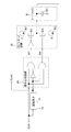
図16は、従来の遅延ロックドループ回路の構成を示す。遅延回路100は、直列に接続された4個の遅延素子101を有し、基準クロック信号CLKrを受け、一周期遅延した遅延クロック信号CLKdを出力する。位相比較器102は、基準クロック信号CLKrと遅延クロック信号CLKdとの位相を比較し、この比較結果に応じて信号UP及びDNを出力する。チャージポンプ回路(ループフィルタを含む)103は、信号UP及びDNに基づいて遅延回路100を制御する。上記構成の遅延ロックドループ回路は、遅延クロック信号CLKdの位相が基準クロック信号CLKrの位相から一周期遅延したときに安定し、このとき、遅延クロック信号CLKdの遅延がロックされる(例えば、特許文献1参照)。
FIG. 16 shows a configuration of a conventional delay locked loop circuit. The
上記構成の遅延ロックドループ回路では、遅延回路100における初段の遅延素子101から1/4位相(90°)遅れのクロック信号が出力される。また、3段目の遅延素子101から3/4位相(270°)遅れのクロック信号が出力される。
従来の遅延ロックドループ回路では、基準クロック信号CLKrと遅延素子101のドライブ能力や負荷容量が異なるため、1/4位相及び3/4位相の精度を上げにくいという問題がある。
The conventional delay locked loop circuit has a problem that it is difficult to improve the accuracy of the ¼ phase and the ¾ phase because the drive capability and load capacity of the reference clock signal CLKr and the
また、従来の遅延ロックドループ回路では、遅延クロック信号は、基準クロック信号のデューティ比にかかわらず、基準クロック信号から1/4位相又は3/4位相遅れのクロック信号として生成される。このため、例えば、基準クロック信号のデューティ比が25%よりも小さい場合、基準クロック信号のオンデューティ中に1/4位相遅れのクロック信号の立ち上がり又は立ち上がりが発生しないため、DDRでは使用することができなくなる。このように、従来の遅延ロックドループ回路は、デューティ比が50%ではない基準クロック信号には対応できないおそれがある。 Further, in the conventional delay locked loop circuit, the delayed clock signal is generated as a clock signal that is 1/4 phase or 3/4 phase delayed from the reference clock signal, regardless of the duty ratio of the reference clock signal. For this reason, for example, when the duty ratio of the reference clock signal is smaller than 25%, the rising or rising of the 1/4 phase delayed clock signal does not occur during the on-duty of the reference clock signal. become unable. As described above, the conventional delay locked loop circuit may not be able to cope with the reference clock signal whose duty ratio is not 50%.
また、従来の遅延ロックドループ回路では、原理的に、遅延クロック信号CLKdの遅延がロックされた後も極めて短いパルス幅の信号UP及びDNが出力される。したがって、従来の遅延ロックドループ回路には定常ジッタが存在する。定常ジッタを抑制するには遅延ゲインを小さくすることが考えられるが、遅延ゲインを小さくすると、遅延がロックされるまでの応答速度、すなわち、ロッキングタイムが遅くなってしまう。また、ループフィルタの容量を大きくしてフィルタ時定数を大きくすることで定常ジッタを抑制することも考えられるが、この場合、回路規模が大きくなってしまう。 Further, in the conventional delay locked loop circuit, in principle, signals UP and DN having extremely short pulse widths are output even after the delay of the delayed clock signal CLKd is locked. Therefore, steady jitter exists in the conventional delay locked loop circuit. In order to suppress the steady jitter, it is conceivable to reduce the delay gain. However, if the delay gain is reduced, the response speed until the delay is locked, that is, the locking time is delayed. Further, it is conceivable to suppress steady jitter by increasing the capacity of the loop filter and increasing the filter time constant, but in this case, the circuit scale becomes large.
上記問題に鑑み、本発明は、原理的に定常ジッタがなく、基準クロック信号のデューティ比にかかわらず高精度な遅延クロック信号を生成可能な遅延ロックドループ回路を実現することを課題とする。 In view of the above problems, an object of the present invention is to realize a delay-locked loop circuit that can generate a highly accurate delayed clock signal regardless of the duty ratio of the reference clock signal in principle without steady jitter.
上記課題を解決するために本発明が講じた手段は、遅延ロックドループ回路として、基準クロック信号の第1の論理レベルから第2の論理レベルへの第1の変化から遅延して、第1の論理レベルから第2の論理レベルへ変化する遅延クロック信号を生成する遅延素子と、前記基準クロック信号の第1の変化、前記基準クロック信号の前記第2の論理レベルから前記第1の論理レベルへの第2の変化、及び前記遅延クロック信号の変化に応じて相補的に変化する第1及び第2の信号を生成する信号生成回路と、前記第1及び第2の信号に従って、前記基準クロック信号の第1の変化から前記遅延クロック信号の変化までの間、プッシュ動作及びプル動作のいずれか一方である第1の動作を行い、前記遅延クロック信号の変化から前記基準クロック信号の第2の変化までの間、プッシュ動作及びプル動作の他方である第2の動作を行うチャージポンプ回路と、前記チャージポンプ回路の出力を受けるループフィルタとを備えたものとする。ここで、前記遅延素子は、前記ループフィルタの出力に基づいて、前記基準クロック信号の第1の変化から前記遅延クロック信号の変化までの遅延量を制御する。 The means taken by the present invention to solve the above-described problem is a delay locked loop circuit that delays from a first change from a first logic level to a second logic level of a reference clock signal. A delay element for generating a delayed clock signal that changes from a logic level to a second logic level; a first change in the reference clock signal; and from the second logic level of the reference clock signal to the first logic level. A signal generation circuit for generating first and second signals that change complementarily in accordance with a second change of the delay clock signal and a change of the delayed clock signal, and the reference clock signal according to the first and second signals From the first change of the delay clock signal to the change of the delayed clock signal, the first operation which is one of the push operation and the pull operation is performed, and the reference clock is changed from the change of the delayed clock signal. Until a second variation of the signal, and that includes a charge pump circuit for performing a second operation, which is the other of the push operation and the pull operation, a loop filter for receiving an output of said charge pump circuit. Here, the delay element controls a delay amount from the first change of the reference clock signal to the change of the delay clock signal based on the output of the loop filter.
この発明によると、信号生成回路によって、基準クロック信号の第1の論理レベルから第2の論理レベルへの第1の変化及びその逆の第2の変化、並びに、遅延素子によって遅延制御され生成された遅延クロック信号の第1の論理レベルから第2の論理レベルへの変化に応じて相補的に変化する第1及び第2の信号が生成され、これら第1及び第2の信号に従ってチャージポンプ回路がプッシュプル動作をし、その出力はループフィルタによって平滑化され、その平滑化された出力に基づいて、遅延素子によって遅延クロック信号の遅延制御が行われる。ここで、遅延クロック信号の変化は、基準クロック信号の第1の変化から、遅延素子によって制御される量だけ遅延して生じる。したがって、本発明に係る遅延ロックドループ回路では、遅延のロッキングポイントは、基準クロック信号の第1の変化から所定量だけ遅延した唯一のところとなり、また、基準クロック信号のデューティ比にかかわらず、基準クロック信号のオンデューティ又はオフデューティ中に立ち上がり又は立ち下がりが生じる遅延クロック信号が生成される。また、本発明に係る遅延ロックドループ回路では、原理的に、定常状態において、遅延クロック信号のジッタの原因となるパルスが出力されない。したがって、ジッタの抑制を目的としてフィルタ時定数を大きくする必要がなく、ループフィルタの小型化、ひいては遅延ロックドループ回路全体の小型化が実現される。 According to the present invention, the signal generation circuit generates the first change of the reference clock signal from the first logic level to the second logic level and vice versa, and the delay element controls the delay by the delay element. First and second signals that change complementarily in response to the change of the delayed clock signal from the first logic level to the second logic level are generated, and the charge pump circuit is generated according to the first and second signals. Performs a push-pull operation, its output is smoothed by a loop filter, and delay control of the delay clock signal is performed by a delay element based on the smoothed output. Here, the change of the delayed clock signal is generated with a delay by an amount controlled by the delay element from the first change of the reference clock signal. Therefore, in the delay locked loop circuit according to the present invention, the delay locking point is the only place delayed by a predetermined amount from the first change of the reference clock signal, and the reference clock signal is independent of the duty ratio of the reference clock signal. A delayed clock signal is generated that rises or falls during on-duty or off-duty of the clock signal. Further, in principle, the delay locked loop circuit according to the present invention does not output a pulse that causes jitter of the delayed clock signal in a steady state. Therefore, it is not necessary to increase the filter time constant for the purpose of suppressing jitter, and the loop filter can be downsized and the entire delay locked loop circuit can be downsized.
具体的には、前記信号生成回路は、前記第1の信号として、前記基準クロック信号の第1の変化から前記遅延クロック信号の変化までの間、第1の論理レベルとなり、これ以外のとき、第2の論理レベルとなる信号を生成し、前記第2の信号として、前記遅延クロック信号の変化から前記基準クロック信号の第2の変化までの間、第1の論理レベルとなり、これ以外のとき、第2の論理レベルとなる信号を生成する。また、前記チャージポンプ回路は、前記第1の動作に係る第1の電流を供給する第1の電流源と、前記第2の動作に係る第2の電流を供給する第2の電流源と、前記第1の信号が前記第1の論理レベルのとき、前記第1の電流を通電し、前記第2の論理レベルのとき、前記第1の電流を遮断する第1のスイッチと、前記第2の信号が前記第1の論理レベルのとき、前記第2の電流を通電し、前記第2の論理レベルのとき、前記第2の電流を遮断する第2のスイッチとを有する。また、前記遅延素子は、前記ループフィルタの出力電圧の増大及び減少のいずれか一方に従って前記遅延量を減少し、他方に従って前記遅延量を増大する制御を行う。 Specifically, the signal generation circuit has the first logic level as the first signal from the first change of the reference clock signal to the change of the delayed clock signal, and at other times, A signal having a second logic level is generated, and the second signal is set to the first logic level from the change of the delayed clock signal to the second change of the reference clock signal. , A signal having a second logic level is generated. The charge pump circuit includes: a first current source that supplies a first current related to the first operation; a second current source that supplies a second current related to the second operation; A first switch for energizing the first current when the first signal is at the first logic level, and blocking the first current when the first signal is at the second logic level; And a second switch for energizing the second current when the signal is at the first logic level and interrupting the second current when the signal is at the second logic level. The delay element performs control to decrease the delay amount according to one of increase and decrease of the output voltage of the loop filter and increase the delay amount according to the other.
この発明によると、チャージポンプ回路のプッシュ動作及びプル動作に係る電荷量が平衡となるように遅延ロックドループ回路が動作する。したがって、プッシュ動作及びプル動作のそれぞれに係る電流量を適宜設定することにより、所望のロッキングポイントを設定することができる。 According to the present invention, the delay locked loop circuit operates so that the charge amounts related to the push operation and the pull operation of the charge pump circuit are balanced. Therefore, a desired locking point can be set by appropriately setting the amount of current related to each of the push operation and the pull operation.
より具体的には、前記第1の電流の大きさと前記第2の電流の大きさとは等しい。これにより、基準クロック信号のデューティ比にかかわらず、基準クロック信号のオンデューティ又はオフデューティの半分の時点で立ち上がり又は立ち下がりが生じる遅延クロック信号が生成される。 More specifically, the magnitude of the first current is equal to the magnitude of the second current. As a result, a delayed clock signal that rises or falls at the time of half of the on-duty or off-duty of the reference clock signal is generated regardless of the duty ratio of the reference clock signal.
また、具体的には、前記信号生成回路は、前記第1の信号として、前記基準クロック信号の第1の変化から前記遅延クロック信号の変化までの間、第1の論理レベルとなり、これ以外のとき、第2の論理レベルとなる信号を生成し、前記第2の信号として、前記基準クロックの第1の変化から第2の変化までの間、第1の論理レベルとなり、これ以外のとき、第2の論理レベルとなる信号を生成する。また、前記チャージポンプ回路は、前記第1の動作に係る第1の電流を供給する第1の電流源と、前記第2の動作に係る第2の電流を供給する第2の電流源と、前記第1の信号が前記第1の論理レベルのとき、前記第1の電流を通電し、前記第2の論理レベルのとき、前記第1の電流を遮断する第1のスイッチと、前記第2の信号が前記第1の論理レベルのとき、前記第2の電流を通電し、前記第2の論理レベルのとき、前記第2の電流を遮断する第2のスイッチとを有する。また、前記遅延素子は、前記ループフィルタの出力電圧の増大及び減少のいずれか一方に従って前記遅延量を減少し、他方に従って前記遅延量を増大する制御を行う。 More specifically, the signal generation circuit has a first logic level as the first signal from the first change of the reference clock signal to the change of the delayed clock signal. A second logic level signal is generated, and the second signal is set to the first logic level from the first change to the second change of the reference clock; otherwise, A signal having the second logic level is generated. The charge pump circuit includes: a first current source that supplies a first current related to the first operation; a second current source that supplies a second current related to the second operation; A first switch for energizing the first current when the first signal is at the first logic level, and blocking the first current when the first signal is at the second logic level; And a second switch for energizing the second current when the signal is at the first logic level and interrupting the second current when the signal is at the second logic level. The delay element performs control to decrease the delay amount according to one of increase and decrease of the output voltage of the loop filter and increase the delay amount according to the other.
この発明によると、チャージポンプ回路のプッシュ動作及びプル動作に係る電荷量が平衡となるように遅延ロックドループ回路が動作する。したがって、プッシュ動作及びプル動作のそれぞれに係る電流量を適宜設定することにより、所望のロッキングポイントを設定することができる。また、第2の信号として基準クロック信号をそのままか又はその反転を用いることができるため、信号生成回路の構成が比較的容易になり、回路規模が縮小する。 According to the present invention, the delay locked loop circuit operates so that the charge amounts related to the push operation and the pull operation of the charge pump circuit are balanced. Therefore, a desired locking point can be set by appropriately setting the amount of current related to each of the push operation and the pull operation. Further, since the reference clock signal can be used as it is or as an inversion thereof as the second signal, the configuration of the signal generation circuit becomes relatively easy, and the circuit scale is reduced.
より具体的には、前記第1の電流の大きさは、前記第2の電流の大きさの2倍に相当する。これにより、基準クロック信号のデューティ比にかかわらず、基準クロック信号のオンデューティ又はオフデューティの半分の時点で立ち上がり又は立ち下がりが生じる遅延クロック信号が生成される。 More specifically, the magnitude of the first current corresponds to twice the magnitude of the second current. As a result, a delayed clock signal that rises or falls at the time of half of the on-duty or off-duty of the reference clock signal is generated regardless of the duty ratio of the reference clock signal.
また、具体的には、前記信号生成回路は、前記第1の信号として、前記基準クロック信号の第1の変化から前記遅延クロック信号の変化までの間、第1の論理レベルとなり、これ以外のとき、第2の論理レベルとなる信号を生成し、前記第2の信号として、前記基準クロックの第1の変化から第2の変化までの間、第1の論理レベルとなり、これ以外のとき、第2の論理レベルとなる信号を生成する。また、前記チャージポンプ回路は、前記第1の動作に係る第1及び第4の電流をそれぞれ供給する第1及び第4の電流源と、前記第2の動作に係る第2及び第3の電流をそれぞれ供給する第2及び第3の電流源と、前記第1の信号が前記第1の論理レベルのとき、前記第1の電流を通電し、前記第2の論理レベルのとき、前記第1の電流を遮断する第1のスイッチと、前記第2の信号が前記第1の論理レベルのとき、前記第2の電流を通電し、前記第2の論理レベルのとき、前記第2の電流を遮断する第2のスイッチと、前記第1の信号が前記第1の論理レベルのとき、前記第3の電流を遮断し、前記第2の論理レベルのとき、前記第3の電流を通電する第3のスイッチと、前記第2の信号が前記第1の論理レベルのとき、前記第4の電流を遮断し、前記第2の論理レベルのとき、前記第4の電流を通電する第4のスイッチとを有する。また、前記遅延素子は、前記ループフィルタの出力電圧の増大及び減少のいずれか一方に従って前記遅延量を減少し、他方に従って前記遅延量を増大する制御を行う。 More specifically, the signal generation circuit has a first logic level as the first signal from the first change of the reference clock signal to the change of the delayed clock signal. A second logic level signal is generated, and the second signal is set to the first logic level from the first change to the second change of the reference clock; otherwise, A signal having the second logic level is generated. The charge pump circuit includes first and fourth current sources for supplying first and fourth currents related to the first operation, and second and third currents related to the second operation. And when the first signal is at the first logic level, the first current is applied, and when the first signal is at the second logic level, the first current source A first switch that cuts off the current, and when the second signal is at the first logic level, the second current is passed, and when the second signal is at the second logic level, the second current is A second switch that shuts off, and a third current that shuts off the third current when the first signal is at the first logic level, and that conducts the third current when the first signal is at the second logic level. 3 switch and when the second signal is at the first logic level, the fourth current is Cross, and when the second logic level, and a fourth switch for energizing said fourth current. The delay element performs control to decrease the delay amount according to one of increase and decrease of the output voltage of the loop filter and increase the delay amount according to the other.
この発明によると、チャージポンプ回路のプッシュ動作及びプル動作に係る電荷量が平衡となるように遅延ロックドループ回路が動作する。したがって、プッシュ動作及びプル動作のそれぞれに係る電流量を適宜設定することにより、所望のロッキングポイントを設定することができる。また、第2の信号として基準クロック信号又はその反転をそのまま用いることができるため、信号生成回路の構成が比較的容易になり、回路規模が縮小する。 According to the present invention, the delay locked loop circuit operates so that the charge amounts related to the push operation and the pull operation of the charge pump circuit are balanced. Therefore, a desired locking point can be set by appropriately setting the amount of current related to each of the push operation and the pull operation. Further, since the reference clock signal or its inversion can be used as it is as the second signal, the configuration of the signal generation circuit becomes relatively easy and the circuit scale is reduced.
より具体的には、前記第2から第4の電流の大きさはいずれも等しく、かつ、前記第1の電流の大きさは、前記第2から第4の電流の大きさの3倍に相当する。これにより、基準クロック信号のデューティ比にかかわらず、基準クロック信号のオンデューティ又はオフデューティの半分の時点で立ち上がり又は立ち下がりが生じる遅延クロック信号が生成される。 More specifically, the magnitudes of the second to fourth currents are all equal, and the magnitude of the first current is equivalent to three times the magnitude of the second to fourth currents. To do. As a result, a delayed clock signal that rises or falls at the time of half of the on-duty or off-duty of the reference clock signal is generated regardless of the duty ratio of the reference clock signal.
また、具体的には、前記信号生成回路は、前記第1の信号として、前記基準クロック信号の第1の変化から前記遅延クロック信号の変化までの間、第1の論理レベルとなり、これ以外のとき、第2の論理レベルとなる信号を生成し、前記第2の信号として、前記基準クロックの第1の変化から第2の変化までの間、第1の論理レベルとなり、これ以外のとき、第2の論理レベルとなる信号を生成する。また、前記チャージポンプ回路は、前記第1の動作に係る第1、第4及び第5の電流をそれぞれ供給する第1、第4及び第5の電流源と、前記第2の動作に係る第2及び第3の電流をそれぞれ供給する第2及び第3の電流源と、前記第1の信号が前記第1の論理レベルのとき、前記第1の電流を通電し、前記第2の論理レベルのとき、前記第1の電流を遮断する第1のスイッチと、前記第2の信号が前記第1の論理レベルのとき、前記第2の電流を通電し、前記第2の論理レベルのとき、前記第2の電流を遮断する第2のスイッチと、前記第1の信号が前記第1の論理レベルのとき、前記第3の電流を遮断し、前記第2の論理レベルのとき、前記第3の電流を通電する第3のスイッチと、前記第2の信号が前記第1の論理レベルのとき、前記第4の電流を遮断し、前記第2の論理レベルのとき、前記第4の電流を通電する第4のスイッチとを有する。また、前記遅延素子は、前記ループフィルタの出力電圧の増大及び減少のいずれか一方に従って前記遅延量を減少し、他方に従って前記遅延量を増大する制御を行う。 More specifically, the signal generation circuit has a first logic level as the first signal from the first change of the reference clock signal to the change of the delayed clock signal. A second logic level signal is generated, and the second signal is set to the first logic level from the first change to the second change of the reference clock; otherwise, A signal having the second logic level is generated. The charge pump circuit includes first, fourth, and fifth current sources that respectively supply first, fourth, and fifth currents related to the first operation, and a second operation related to the second operation. And second and third current sources for supplying second and third currents, respectively, and when the first signal is at the first logic level, the first current is applied and the second logic level is applied. A first switch that cuts off the first current, and when the second signal is at the first logic level, the second current is energized, and when the second signal is at the second logic level, A second switch that cuts off the second current, and cuts off the third current when the first signal is at the first logic level, and the third switch when the first signal is at the second logic level. A third switch for energizing the current, and when the second signal is at the first logic level, Blocks the fourth current, when the second logic level, and a fourth switch for energizing said fourth current. The delay element performs control to decrease the delay amount according to one of increase and decrease of the output voltage of the loop filter and increase the delay amount according to the other.
この発明によると、チャージポンプ回路のプッシュ動作及びプル動作に係る電荷量が平衡となるように遅延ロックドループ回路が動作する。したがって、プッシュ動作及びプル動作のそれぞれに係る電流量を適宜設定することにより、所望のロッキングポイントを設定することができる。また、第2の信号として基準クロック信号又はその反転をそのまま用いることができるため、信号生成回路の構成が比較的容易になり、回路規模が縮小する。 According to the present invention, the delay locked loop circuit operates so that the charge amounts related to the push operation and the pull operation of the charge pump circuit are balanced. Therefore, a desired locking point can be set by appropriately setting the amount of current related to each of the push operation and the pull operation. Further, since the reference clock signal or its inversion can be used as it is as the second signal, the configuration of the signal generation circuit becomes relatively easy and the circuit scale is reduced.
より具体的には、前記第1の電流の大きさと前記第3の電流の大きさとは等しく、前記第2、第4及び第5の電流の大きさはいずれも等しく、かつ、前記第1及び第3の電流の大きさは、前記第2、第4及び第5の電流の大きさの2倍に相当する。これにより、基準クロック信号のデューティ比にかかわらず、基準クロック信号のオンデューティ又はオフデューティの半分の時点で立ち上がり又は立ち下がりが生じる遅延クロック信号が生成される。 More specifically, the magnitude of the first current and the magnitude of the third current are equal, the magnitudes of the second, fourth and fifth currents are all equal, and the first and The magnitude of the third current corresponds to twice the magnitude of the second, fourth and fifth currents. As a result, a delayed clock signal that rises or falls at the time of half of the on-duty or off-duty of the reference clock signal is generated regardless of the duty ratio of the reference clock signal.
また、具体的には、前記信号生成回路は、前記第1の信号として、前記基準クロック信号の第1の変化から前記遅延クロック信号の変化までの間、第1の電圧となり、これ以外のとき、第2の電圧となる信号を生成し、前記第2の信号として、前記基準クロックの第1の変化から第2の変化までの間、前記第2の電圧となり、これ以外のとき、前記第1の電圧となる信号を生成する。また、前記チャージポンプ回路は、前記第1の信号を受ける第1の抵抗と、前記第2の信号を受ける第2の抵抗と、一端が前記第1及び第2の抵抗の接続箇所に接続され、他端に第3の電圧が与えられた第3の抵抗とを有する。また、前記ループフィルタは、容量と、負帰還部分に前記容量が接続され、反転入力端が前記チャージポンプ回路における第1から第3の抵抗の接続箇所に接続され、非反転入力端に第4の電圧が与えられた演算増幅器とを有する。また、前記遅延素子は、前記ループフィルタにおける演算増幅器の出力電圧の増大及び減少のいずれか一方に従って前記遅延量を減少し、他方に従って前記遅延量を増大する制御を行う。 More specifically, the signal generation circuit has the first voltage as the first signal from the first change of the reference clock signal to the change of the delayed clock signal, and at other times The second voltage is generated, and the second signal is the second voltage during the period from the first change to the second change of the reference clock. Otherwise, the second voltage is the second voltage. A signal having a voltage of 1 is generated. The charge pump circuit includes a first resistor that receives the first signal, a second resistor that receives the second signal, and one end connected to a connection portion of the first and second resistors. And a third resistor to which the third voltage is applied at the other end. In the loop filter, the capacitor is connected to a negative feedback portion, the inverting input terminal is connected to the connection point of the first to third resistors in the charge pump circuit, and the fourth terminal is connected to the non-inverting input terminal. And an operational amplifier to which the voltage is given. The delay element performs control to decrease the delay amount according to one of increase and decrease of the output voltage of the operational amplifier in the loop filter and increase the delay amount according to the other.
この発明によると、チャージポンプ回路のプッシュ動作及びプル動作の切り替えの際にスイッチングノイズが発生しないため、電流精度の劣化がない。また、チャージポンプ回路が比較的低電圧で動作可能となる。 According to the present invention, since the switching noise is not generated when the charge pump circuit is switched between the push operation and the pull operation, the current accuracy is not deteriorated. In addition, the charge pump circuit can operate at a relatively low voltage.
より具体的には、前記第2の電圧と前記第3の電圧とは等しく、前記第4の電圧は、前記第1の電圧と前記第2の電圧との中間に相当する電圧であり、前記第2の抵抗の抵抗値と前記第3の抵抗の抵抗値とは等しく、前記第1の抵抗の抵抗値は、前記第2及び第3の抵抗の抵抗値の半分に相当する。これにより、基準クロック信号のデューティ比にかかわらず、基準クロック信号のオンデューティ又はオフデューティの半分の時点で立ち上がり又は立ち下がりが生じる遅延クロック信号が生成される。 More specifically, the second voltage and the third voltage are equal, and the fourth voltage is a voltage corresponding to an intermediate point between the first voltage and the second voltage, The resistance value of the second resistor is equal to the resistance value of the third resistor, and the resistance value of the first resistor corresponds to half of the resistance values of the second and third resistors. As a result, a delayed clock signal that rises or falls at the time of half of the on-duty or off-duty of the reference clock signal is generated regardless of the duty ratio of the reference clock signal.
また、具体的には、前記遅延素子は、直列に接続され、ゲートに前記基準クロック信号を受ける互いに逆極性の第1及び第2のトランジスタ、及びこれらトランジスタの間に接続され、ゲートに前記ループフィルタの出力を受ける第3のトランジスタを有し、前記第1のトランジスタと前記第2のトランジスタとの間の所定ノードの電圧を出力信号とする第1の回路と、前記第1の回路の出力信号の波形を整形する第2の回路とを備えている。 More specifically, the delay element is connected in series, and has a gate connected to the first and second transistors of opposite polarities receiving the reference clock signal, and is connected between the transistors, and the gate is connected to the loop. A first circuit having a third transistor for receiving an output of the filter, wherein the output signal is a voltage at a predetermined node between the first transistor and the second transistor; and an output of the first circuit And a second circuit for shaping the waveform of the signal.
この発明によると、第1の回路の出力信号の電圧は基準クロック信号の変化に応じて変化し、この変化に係る遅延は、第3のトランジスタに形成されるチャネルに応じて変化する。ここで、当該チャネルの形成状態はループフィルタの出力に応じて変化するため、ループフィルタの出力に基づく、第1の回路の出力信号の遅延量が制御可能となる。第1の回路の出力信号には当該遅延に伴い波形に鈍りが生じるが、第2の回路によって波形整形され、また、リンギングも抑制される。これにより、第2の回路から出力された信号は遅延クロック信号として利用可能となる。また、第3のトランジスタのゲート電圧の調整によって上記遅延量が制御できることから、極めて広いロックインレンジが達成される。 According to the present invention, the voltage of the output signal of the first circuit changes according to the change of the reference clock signal, and the delay associated with this change changes according to the channel formed in the third transistor. Here, since the channel formation state changes according to the output of the loop filter, the delay amount of the output signal of the first circuit based on the output of the loop filter can be controlled. Although the waveform of the output signal of the first circuit becomes dull with the delay, the waveform is shaped by the second circuit and ringing is also suppressed. Thus, the signal output from the second circuit can be used as a delayed clock signal. Further, since the delay amount can be controlled by adjusting the gate voltage of the third transistor, an extremely wide lock-in range is achieved.
好ましくは、前記第1の回路は、前記第3のトランジスタに並列に接続された電流源を有する。 Preferably, the first circuit includes a current source connected in parallel to the third transistor.
この発明によると、第3のトランジスタに並列に接続された電流源によって、第1の回路の出力信号に係る電荷移動に最小値の制限が設けられ、特に、第3のトランジスタに流れる電流が比較的小さい場合に、ループフィルタの出力のほんのわずかな変動により遅延クロック信号の遅延量が大幅に変動することによる発振を防止することができる。 According to the present invention, the current source connected in parallel to the third transistor provides a minimum value restriction on the charge transfer related to the output signal of the first circuit. In particular, the current flowing through the third transistor is compared. In the case where the delay time is small, oscillation due to a large variation in the delay amount of the delayed clock signal due to a slight variation in the output of the loop filter can be prevented.
また、具体的には、前記第2の回路は、前記第1の回路の出力信号を受けるインバータと、前記インバータの入力及び出力をそれぞれドレイン及びゲートに受け、ソースに所定の電圧が与えられたトランジスタを有する。 Specifically, the second circuit has an inverter that receives the output signal of the first circuit, an input and an output of the inverter received at a drain and a gate, respectively, and a predetermined voltage is applied to the source. Has a transistor.
この発明によると、第1の回路の出力信号の電圧がインバータの閾値を超えたとき、インバータからその論理反転に相当する信号が出力され、インバータの入出力間に設けられたトランジスタによってインバータ出力が所定の電圧に固定され、第1の回路の出力信号が波形整形される。 According to the present invention, when the voltage of the output signal of the first circuit exceeds the threshold value of the inverter, a signal corresponding to the logical inversion is output from the inverter, and the inverter output is output by the transistor provided between the input and output of the inverter. The output voltage of the first circuit is waveform-shaped while being fixed at a predetermined voltage.
また、好ましくは、上記の遅延ロックドループ回路は、前記遅延素子の遅延量を漸増させて、前記基準クロック信号の第1の変化から前記遅延クロック信号の変化までの遅延をロックする。 Preferably, the delay locked loop circuit gradually increases a delay amount of the delay element to lock a delay from a first change of the reference clock signal to a change of the delay clock signal.
この発明によると、基準クロック信号の第1の変化から遅延クロック信号の変化までの遅延が最小値から次第に増加していく方向に制御される。初期状態における遅延素子の遅延量は最小であり、所望の値と異なるものの、遅延ロックドループ回路の動作開始時からすぐに遅延クロック信号が得られることになる。 According to the present invention, the delay from the first change of the reference clock signal to the change of the delayed clock signal is controlled in the direction of gradually increasing from the minimum value. Although the delay amount of the delay element in the initial state is the minimum and is different from a desired value, a delayed clock signal can be obtained immediately after the start of the operation of the delay locked loop circuit.
一方、本発明が講じた手段は、遅延ロックドループ回路として、共通の基準クロック信号が与えられる、上記の遅延ロックドループ回路である第1及び第2の遅延ロックドループ回路と、前記第1及び第2の遅延ロックドループ回路の出力クロック信号から、前記共通の基準クロック信号の立ち上がりから遅延して立ち上がり及び立ち下がりのいずれか一方の変化が生じる一方、前記共通の基準クロック信号の立ち下がりから遅延して立ち上がり及び立ち下がりの他方の変化が生じる遅延クロック信号を生成するクロック生成回路とを備えたものとする。 On the other hand, according to the present invention, the delay locked loop circuit is provided with a common reference clock signal, and the first and second delay locked loop circuits are the above-described delay locked loop circuits. 2 is delayed from the rising edge of the common reference clock signal from the output clock signal of the delay locked loop circuit 2, while either one of the rising edge and the falling edge is changed, and delayed from the falling edge of the common reference clock signal. And a clock generation circuit for generating a delayed clock signal in which the other change of rising and falling occurs.
この発明によると、第1及び第2の遅延ロックドループ回路に与えられた共通の基準クロック信号のデューティ比にかかわらず、当該共通の基準クロック信号のオンデューティ及びオフデューティ中に論理レベルが変化する遅延クロック信号が生成される。 According to the present invention, the logic level changes during the on-duty and off-duty of the common reference clock signal regardless of the duty ratio of the common reference clock signal applied to the first and second delay locked loop circuits. A delayed clock signal is generated.
具体的には、前記第1の遅延ロックドループ回路は、前記共通の基準クロック信号の立ち上がりから、前記共通の基準クロック信号のオンデューティの半分に相当する期間遅延して、論理レベルが変化するクロック信号を出力するものとする。また、前記第2の遅延ロックドループ回路は、前記共通の基準クロック信号の立ち下がりから、前記共通の基準クロック信号のオフデューティの半分に相当する期間遅延して、論理レベルが変化するクロック信号を出力するものとする。 Specifically, the first delay locked loop circuit delays a period corresponding to half the on-duty of the common reference clock signal from the rising edge of the common reference clock signal, and changes the logic level. A signal shall be output. The second delay locked loop circuit delays a clock signal whose logic level changes by delaying a period corresponding to half of the off-duty of the common reference clock signal from the falling edge of the common reference clock signal. Shall be output.
この発明によると、共通の基準クロック信号のデューティ比にかかわらず、そのデューティ比が補正され、生成される遅延クロック信号のデューティ比は50%となる。 According to the present invention, regardless of the duty ratio of the common reference clock signal, the duty ratio is corrected, and the duty ratio of the generated delayed clock signal is 50%.
また、本発明が講じた手段は、遅延ロックドループ回路として、第1の基準クロック信号が与えられる、上記の遅延ロックドループ回路である第1の遅延ロックドループ回路と、前記第1の基準クロック信号とは逆位相の第2の基準クロック信号が与えられる、上記の記載の遅延ロックドループ回路である第2の遅延ロックドループ回路と、前記第1及び第2の遅延ロックドループ回路の出力クロック信号から、前記第1の基準クロック信号の立ち上がりから遅延して立ち上がり及び立ち下がりのいずれか一方の変化が生じる一方、前記第1の基準クロック信号の立ち下がりから遅延して立ち上がり及び立ち下がりの他方の変化が生じる遅延クロック信号を生成するクロック生成回路とを備えたものとする。 According to the present invention, the delay locked loop circuit is provided with a first reference clock signal. The first delay locked loop circuit, which is the delay locked loop circuit described above, and the first reference clock signal. From the second delay locked loop circuit, which is the delay locked loop circuit described above, and the output clock signals of the first and second delay locked loop circuits. One of the rising and falling changes is delayed from the rising edge of the first reference clock signal, while the other of the rising and falling edges is delayed from the falling edge of the first reference clock signal. And a clock generation circuit for generating a delayed clock signal in which the above occurs.
この発明によると、第1及び第2の遅延ロックドループ回路の極性を同一にすることができ、回路設計が容易になる。 According to the present invention, the polarities of the first and second delay locked loop circuits can be made the same, and the circuit design is facilitated.
具体的には、前記第1の遅延ロックドループ回路は、前記第1の基準クロック信号の立ち上がりから、前記第1の基準クロック信号のオンデューティの半分に相当する期間遅延して、論理レベルが変化するクロック信号を出力するものとする。また、前記第2の遅延ロックドループ回路は、前記第2の基準クロック信号の立ち上がりから、前記第2の基準クロック信号のオンデューティの半分に相当する期間遅延して、論理レベルが変化するクロック信号を出力するものとする。 Specifically, the first delay locked loop circuit delays a period corresponding to half of the on-duty of the first reference clock signal from the rising edge of the first reference clock signal, and the logic level changes. The clock signal to be output is output. The second delay locked loop circuit is a clock signal whose logic level changes after being delayed for a period corresponding to half of the on-duty of the second reference clock signal from the rising edge of the second reference clock signal. Is output.
この発明によると、第1の基準クロック信号のデューティ比にかかわらず、そのデューティ比が補正され、生成される遅延クロック信号のデューティ比は50%となる。 According to the present invention, regardless of the duty ratio of the first reference clock signal, the duty ratio is corrected, and the duty ratio of the generated delayed clock signal is 50%.
以上のように、本発明によると、原理的に定常ジッタがなく、基準クロック信号のデューティ比にかかわらず高精度な遅延クロック信号が生成される。このため、時定数の大きなループフィルタを特に設ける必要がなくなり、遅延ロックドループ回路の回路規模が縮小する。 As described above, according to the present invention, there is no steady jitter in principle, and a highly accurate delayed clock signal is generated regardless of the duty ratio of the reference clock signal. Therefore, it is not necessary to provide a loop filter having a large time constant, and the circuit scale of the delay locked loop circuit is reduced.
以下、本発明を実施するための最良の形態について、図面を参照しながら説明する。 The best mode for carrying out the present invention will be described below with reference to the drawings.
(第1の実施形態)
図1は、本発明の第1の実施形態に係る遅延ロックドループ回路の構成を示す。本実施形態に係る遅延ロックドループ回路は、遅延素子10、信号生成回路20、チャージポンプ回路30、及びループフィルタ40を備えている。遅延素子10は、基準クロック信号CLKrを受け、遅延クロック信号CLKdを出力する。遅延クロック信号CLKdの遅延量は、ループフィルタ40から出力された制御電圧Vcによって制御される。信号生成回路20は、基準クロック信号CLKrと遅延クロック信号CLKdの反転との論理積を信号UPとして、また、基準クロック信号CLKrと遅延クロック信号CLKdとの論理積を信号DNとして、それぞれ出力する。チャージポンプ回路30は、電流源301、電流源301が供給する電流I1の通電/遮断を信号UPに従って制御するスイッチ302、電流源303、及び、電流源303が供給する電流I2の通電/遮断を信号DNに従って制御するスイッチ304を備え、信号UPがHiレベルのとき、電流I1を外部へ出力し(プッシュ動作)、信号DNがHiレベルのとき、電流I2を外部から引き込む(プル動作)。ループフィルタ40は、容量401を備え、チャージポンプ回路30の出力を受け、これを積分して制御電圧Vcを生成する。
(First embodiment)
FIG. 1 shows a configuration of a delay locked loop circuit according to a first embodiment of the present invention. The delay locked loop circuit according to the present embodiment includes a
図2は、遅延素子10の構成を示す。遅延素子10において、反転回路11は、遅延素子10の入力信号INを受け、これを論理反転して信号INVを出力する。具体的には、反転回路11は、直列に接続されたPMOSトランジスタ111及びNMOSトランジスタ112、これら二つのトランジスタの間に接続されたNMOSトランジスタ113、及びトランジスタ113に並列に接続されたNMOSトランジスタ114を備えている。トランジスタ111及び112のそれぞれのゲートには信号INが与えられ、トランジスタ111及び113の接続箇所から信号INVが出力される。また、トランジスタ113のゲートにはループフィルタ40から出力された制御電圧Vcが与えられ、トランジスタ114のゲートには所定の電圧が与えられる。一方、波形整形回路12は、信号INVの波形を整形し、遅延素子10の出力信号OUTを生成する。具体的には、波形整形回路12は、信号INVを受け、信号OUTを出力するインバータ121、及びドレイン及びゲートがそれぞれインバータ121の入力端及び出力端に接続され、ソースに所定の電圧、例えば、グランド電圧が与えられたNMOSトランジスタ122を備えている。
FIG. 2 shows the configuration of the
反転回路11において、信号INがLoレベルのとき、スイッチとしてのトランジスタ111及び112はそれぞれ導通状態及び非導通状態となり、反転回路11の出力先には電源ノードから電荷が供給され、信号INVはHiレベルとなる。一方、信号INがHiレベルのとき、トランジスタ111及び112はそれぞれ非導通状態及び導通状態となり、出力先に供給された電荷は接地ノードに引き抜かれ、信号INVはLoレベルとなる。
In the inverting
図3は、遅延素子10のタイミングチャートを示す。信号INが立ち下がると、信号INVは、すぐさまLoレベルからHiレベルへ変化する。これに対して、信号INが立ち上がっても、信号INVは、すぐにはHiレベルからLoレベルへ変化せずに比較的なだらかに変化する。これは、トランジスタ113及び114によって、接地ノードへの電荷引き抜きに制限が加えられることによる。このように波形に鈍りがある信号INVは、波形整形回路12によって波形整形され、急峻な立ち上がり及び立ち下がりを有する信号OUTとなって出力される。また、波形整形回路12は、信号INVに生じるリンギングを抑制するといった効果を奏する。
FIG. 3 shows a timing chart of the
上述したように、トランジスタ113及び114によって接地ノードへの電荷引き抜きに制限が加えられた結果、信号OUTの立ち上がりは、信号INが立ち上がってからある程度遅延して発生する。ここで、制御電圧Vcを適宜調整することによって、トランジスタ113に形成されるチャネルの状態が変化し、信号INVのHiレベルからLoレベルへの変化の速度が変化し、結果として、信号OUTの遅延量が調整される。なお、トランジスタ114は一定の大きさの電流を引き込む電流源として動作する。すなわち、接地ノードへの電荷引き抜きに関して最小値の制限を設けている。この制限がない場合、トランジスタ113に流れる電流が比較的小さい場合に、制御電圧Vcがほんのわずか変化することより、遅延クロック信号CLKdの遅延量が大幅に変化してしまい、発振してしまうおそれがあるからである。
As described above, as a result of limiting the charge extraction to the ground node by the
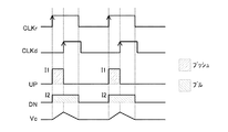
図4は、本実施形態に係る遅延ロックドループ回路のタイミングチャートを示す。基準クロック信号CLKr及び遅延クロック信号CLKdは、それぞれ、図3に示した信号IN及びOUTに相当する。信号UPは、基準クロック信号CLKrの立ち上がりから遅延クロック信号CLKdの立ち上がりまでの期間、Hiレベルとなる。信号DNは、遅延クロック信号CLKdの立ち上がりから基準クロック信号CLKrの立ち下がりまでの期間、Hiレベルとなる。すなわち、信号UP及びDNは、遅延クロック信号CLKdの立ち上がりを境として、基準クロック信号CLKrのオンデューティの前半及び後半の期間、それぞれHiレベルとなる。なお、図4に示したタイミングチャートにおいて、信号UP及びDNに重ねて、チャージポンプ回路30から外部に向かって流れる電流(プッシュ電流)及び外部からチャージポンプ回路30に向かって流れる電流(プル電流)をその大きさとともに平行斜線で表示している。
FIG. 4 is a timing chart of the delay locked loop circuit according to the present embodiment. The reference clock signal CLKr and the delayed clock signal CLKd correspond to the signals IN and OUT shown in FIG. 3, respectively. The signal UP becomes Hi level during the period from the rise of the reference clock signal CLKr to the rise of the delayed clock signal CLKd. The signal DN is at the Hi level during the period from the rising edge of the delayed clock signal CLKd to the falling edge of the reference clock signal CLKr. That is, the signals UP and DN are at the Hi level during the first half and the second half of the on-duty of the reference clock signal CLKr with the rising edge of the delayed clock signal CLKd as a boundary. Incidentally, in the timing chart shown in FIG. 4, to overlap the signals UP and DN, current flowing from the
基準クロック信号CLKrが立ち上がると信号UPがHiレベルとなり、チャージポンプ回路30からループフィルタ40に電流I1が供給され、制御電圧Vcは漸増する。制御電圧Vcが比較的低い場合、遅延クロック信号CLKdの遅延量は比較的大きく、逆に、制御電圧Vcが比較的高い場合、遅延クロック信号CLKdの遅延量は比較的小さい。したがって、制御電圧Vcの増大は、遅延クロック信号CLKdの遅延量を減少させる方向に働き、基準クロック信号CLKrが立ち上がってからある程度の時間が経過したときに、遅延クロック信号CLKdが立ち上がる。この結果、信号DNがHiレベルとなり、ループフィルタ40からチャージポンプ回路30に電流I2が引き込まれ、制御電圧Vcは漸減して元のレベルに戻る。
When the reference clock signal CLKr rises, the signal UP becomes Hi level, the current I1 is supplied from the
本実施形態に係る遅延ロックドループ回路では、遅延クロック信号CLKdの立ち上がりは、基準クロック信号CLKrのオンデューティをある比率で内分した時点で発生するが、この比率は、電流I1及びI2の関係によって決まる。すなわち、本実施形態に係る遅延ロックドループ回路では、チャージポンプ回路30によるプッシュ動作及びプル動作に係る電荷量が平衡するようにフィードバックシステムが作用し、信号UPと信号DNとのHi期間の比が電流I1と電流I2の逆数比となったところでシステムが安定する。したがって、電流I1及びI2の大きさを適宜設定することによって、遅延クロック信号CLKdが基準クロック信号CLKrのオンデューティを所望の比率で内分する時点で立ち上がるように調整することができる。
In the delay locked loop circuit according to the present embodiment, the rising edge of the delayed clock signal CLKd occurs when the on-duty of the reference clock signal CLKr is internally divided by a certain ratio. This ratio depends on the relationship between the currents I1 and I2. Determined. That is, in the delay locked loop circuit according to the present embodiment, the feedback system acts so that the charge amount related to the push operation and the pull operation by the
特に、電流I1及びI2を等しく設定した場合、遅延クロック信号CLKdの立ち上がりは、基準クロック信号CLKrのオンデューティのちょうど半分の時点で生じる。すなわち、基準クロック信号CLKrのデューティ比が50%であるか否かにかかわらず、基準クロック信号CLKrのオンデューティの半分の時点で立ち上がりが生じる遅延クロック信号CLKdを得ることができる。 In particular, when the currents I1 and I2 are set to be equal, the rising edge of the delayed clock signal CLKd occurs at a point that is exactly half the on-duty of the reference clock signal CLKr. In other words, regardless of whether the duty ratio of the reference clock signal CLKr is 50%, it is possible to obtain the delayed clock signal CLKd that rises at a time point that is half the on-duty of the reference clock signal CLKr.
また、従来の遅延ロックドループ回路では定常状態において信号UP及びDNが出力されないのが理想であるが、原理上、実際にはごく短いパルスが出力され、これが定常ジッタの原因となっていたのに対して、本実施形態に係る遅延ロックドループ回路では、定常状態において、チャージポンプ回路30によるプッシュ動作及びプル動作に係る電荷量が平衡となるように信号UP及びDNが常に出力される。これにより、制御電圧Vcは、図4に示したように漸増、漸減を繰り返すが、遅延素子10の遅延量は、漸増部分の電圧軌跡で決定される。したがって、本実施形態に係る遅延ロックドループ回路では、原理上、定常ジッタの原因が発生せず、ジッタ特性に極めて優れた出力、すなわち、遅延クロック信号を得ることができる。
In addition, in the conventional delay locked loop circuit, it is ideal that the signals UP and DN are not output in a steady state, but in principle, a very short pulse is actually output, which causes a steady jitter. On the other hand, in the delay locked loop circuit according to the present embodiment, in the steady state, the signals UP and DN are always output so that the charge amounts related to the push operation and the pull operation by the
以上、本実施形態によると、原理的に定常ジッタがなく、基準クロック信号のデューティ比にかかわらず高精度な遅延クロック信号を生成することができる。 As described above, according to the present embodiment, there is no steady jitter in principle, and a highly accurate delayed clock signal can be generated regardless of the duty ratio of the reference clock signal.
なお、遅延ロックドループ回路を、上記説明とは逆の論理で動作するように構成してもよい。 Note that the delay locked loop circuit may be configured to operate with a logic opposite to that described above.
(第2の実施形態)
図5は、本発明の第2の実施形態に係る遅延ロックドループ回路の構成を示す。本実施形態に係る遅延ロックドループ回路は、第1の実施形態とは異なる構成の信号生成回路20を備えている。本実施形態に係る信号生成回路20は、基準クロック信号CLKrと遅延クロック信号CLKdの反転との論理積を信号UPとして、また、基準クロック信号CLKrを信号DNとして、それぞれ出力する。以下、本実施形態に係る遅延ロックドループ回路について、第1の実施形態に係る遅延ロックドループ回路と異なる点のみを説明する。
(Second Embodiment)
FIG. 5 shows a configuration of a delay locked loop circuit according to the second embodiment of the present invention. The delay locked loop circuit according to the present embodiment includes a
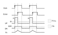
図6は、本実施形態に係る遅延ロックドループ回路のタイミングチャートを示す。信号UPは、基準クロック信号CLKrの立ち上がりから遅延クロック信号CLKdの立ち上がりまでの期間、Hiレベルとなる。信号DNは、基準クロック信号CLKrと同じである。なお、図6に示したタイミングチャートにおいて、信号UP及びDNに重ねて、チャージポンプ回路30から外部に向かって流れる電流(プッシュ電流)及び外部からチャージポンプ回路30に向かって流れる電流(プル電流)をその大きさとともに平行斜線で表示している。
FIG. 6 is a timing chart of the delay locked loop circuit according to the present embodiment. The signal UP becomes Hi level during the period from the rise of the reference clock signal CLKr to the rise of the delayed clock signal CLKd. The signal DN is the same as the reference clock signal CLKr. In the timing chart shown in FIG. 6, the current flowing from the
基準クロック信号CLKrが立ち上がると信号UP及びDNがHiレベルとなり、チャージポンプ回路30におけるスイッチ302及び304が閉じ、チャージポンプ回路30からループフィルタ40に、電流I1と電流I2との差分電流が供給され、制御電圧Vcは漸増する。そして、基準クロック信号CLKrが立ち上がってからある程度の時間が経過したときに、遅延クロック信号CLKdが立ち上がる。この結果、信号UPのみがLoレベルとなり、スイッチ302のみが開き、ループフィルタ40からチャージポンプ回路30に電流I2が引き込まれ、制御電圧Vcは漸減して元のレベルに戻る。したがって、電流I1及びI2の大きさを適宜設定することによって、遅延クロック信号CLKdが基準クロック信号CLKrのオンデューティを所望の比率で内分する時点で立ち上がるように調整することができる。
When the reference clock signal CLKr rises, the signals UP and DN become Hi level, the
特に、電流I1を電流I2の2倍に相当する大きさとなるように設定した場合、チャージポンプ回路30におけるスイッチ302及び304がいずれも閉じたときに供給される電流の大きさと、スイッチ304のみが閉じたときに引き込まれる電流の大きさとが等しくなり、遅延クロック信号CLKdの立ち上がりは、基準クロック信号CLKrのオンデューティのちょうど半分の時点で生じる。
In particular, when the current I1 is set to a magnitude corresponding to twice the current I2, the magnitude of the current supplied when both the
以上、本実施形態によると、第1の実施形態と比較して信号生成回路20の構成が容易になり、遅延ロックドループ回路全体としての回路規模が縮小する。
As described above, according to the present embodiment, the configuration of the
(第3の実施形態)
図7は、本発明の第3の実施形態に係る遅延ロックドループ回路の構成を示す。本実施形態に係る遅延ロックドループ回路は、第2の実施形態とは異なる構成のチャージポンプ回路30を備えている。本実施形態に係るチャージポンプ回路30は、第2の実施形態に係るチャージポンプ回路30に、さらに、電流源305、電流源305が供給する電流I3の通電/遮断を信号UPに従って制御するスイッチ306、電流源307、及び、電流源307が供給する電流I4の通電/遮断を信号DNに従って制御するスイッチ308を備えている。以下、第2の実施形態と異なる点についてのみ説明する。
(Third embodiment)
FIG. 7 shows a configuration of a delay locked loop circuit according to the third embodiment of the present invention. The delay locked loop circuit according to the present embodiment includes a
図8は、本実施形態に係る遅延ロックドループ回路のタイミングチャートを示す。なお、図8に示したタイミングチャートにおいて、信号UP及びDNに重ねて、チャージポンプ回路30から外部に向かって流れる電流(プッシュ電流)及び外部からチャージポンプ回路30に向かって流れる電流(プル電流)をその大きさとともに平行斜線で表示している。
FIG. 8 is a timing chart of the delay locked loop circuit according to the present embodiment. In the timing chart shown in FIG. 8, the current (push current) flowing from the
基準クロック信号CLKrが立ち上がると信号UP及びDNがHiレベルとなり、チャージポンプ回路30におけるスイッチ302及び304が閉じ、チャージポンプ回路30からループフィルタ40に、電流I1と電流I2との差分電流が供給され、制御電圧Vcは漸増する。そして、基準クロック信号CLKrが立ち上がってからある程度の時間が経過したときに、遅延クロック信号CLKdが立ち上がる。この結果、信号UPのみがLoレベルとなり、スイッチ302は開き、代わりにスイッチ306が閉じ、ループフィルタ40からチャージポンプ回路30に、電流I2と電流I3との合計電流が引き込まれ、制御電圧Vcは漸減して元のレベルに戻る。そして、基準クロック信号CLKrが立ち下がったとき、信号DNはLoレベルとなり、スイッチ304は開き、代わりにスイッチ308が閉じ、ループフィルタ40に、電流I3と電流I4との差分電流が供給される。ここで、電流I3と電流I4とが等しいとき、プッシュ電流とプル電流とは相殺され、基準クロック信号CLKrがLoレベルにある間は、チャージポンプ回路30のプッシュプル動作は見かけ上停止する。
When the reference clock signal CLKr rises, the signals UP and DN become Hi level, the
本実施形態に係る遅延ロックドループ回路においても、電流I1〜I4の大きさを適宜設定することによって、遅延クロック信号CLKdが基準クロック信号CLKrのオンデューティを所望の比率で内分する時点で立ち上がるように調整することができる。特に、電流I2〜I4の大きさをいずれも等しくし、電流I1を電流I2〜I4の大きさの3倍に相当する大きさとなるように設定した場合、チャージポンプ回路30におけるスイッチ302及び304が閉じたときにループフィルタ40に供給される電流の大きさと、スイッチ304及び306が閉じたときにループフィルタ40から引き込まれる電流の大きさとが等しくなり、遅延クロック信号CLKdの立ち上がりは、基準クロック信号CLKrのオンデューティのちょうど半分の時点で生じる。
Also in the delay locked loop circuit according to the present embodiment, by appropriately setting the magnitudes of the currents I1 to I4, the delay clock signal CLKd rises when the on-duty of the reference clock signal CLKr is internally divided at a desired ratio. Can be adjusted. In particular, when the magnitudes of the currents I2 to I4 are all equal and the current I1 is set to be a magnitude corresponding to three times the magnitude of the currents I2 to I4, the
以上、本実施形態によると、第1の実施形態と比較して信号生成回路20の構成が容易になり、遅延ロックドループ回路全体としての回路規模が縮小する。
As described above, according to the present embodiment, the configuration of the
(第4の実施形態)
図9は、本発明の第4の実施形態に係る遅延ロックドループ回路の構成を示す。本実施形態に係る遅延ロックドループ回路は、第2及び3の実施形態とは異なる構成のチャージポンプ回路30を備えている。本実施形態に係るチャージポンプ回路30は、第3の実施形態に係るチャージポンプ回路30に、さらに、電流源301と同極性の電流I5を供給する電流源309を備えている。すなわち、本実施形態に係るチャージポンプ回路30では、信号UP及びDNの状態にかかわらず、電流源309から電流I5が常時供給されている。以下、第3の実施形態と異なる点についてのみ説明する。
(Fourth embodiment)
FIG. 9 shows a configuration of a delay locked loop circuit according to the fourth embodiment of the present invention. The delay locked loop circuit according to this embodiment includes a
図10は、本実施形態に係る遅延ロックドループ回路のタイミングチャートを示す。なお、図10に示したタイミングチャートにおいて、信号UP及びDNに重ねて、チャージポンプ回路30から外部に向かって流れる電流(プッシュ電流)及び外部からチャージポンプ回路30に向かって流れる電流(プル電流)をその大きさとともに平行斜線で表示している。
FIG. 10 is a timing chart of the delay locked loop circuit according to the present embodiment. In the timing chart shown in FIG. 10, a current (push current) that flows from the
基準クロック信号CLKrが立ち上がると信号UP及びDNがHiレベルとなり、チャージポンプ回路30におけるスイッチ302及び304が閉じ、チャージポンプ回路30からループフィルタ40に、電流I1と電流I5との合計電流と電流I2との差分電流が供給され、制御電圧Vcは漸増する。そして、基準クロック信号CLKrが立ち上がってからある程度の時間が経過したときに、遅延クロック信号CLKdが立ち上がる。この結果、信号UPのみがLoレベルとなり、スイッチ302は開き、代わりにスイッチ306が閉じ、ループフィルタ40からチャージポンプ回路30に、電流I2と電流I3との合計電流と電流I5との差分電流が引き込まれ、制御電圧Vcは漸減して元のレベルに戻る。そして、基準クロック信号CLKrが立ち下がったとき、信号DNはLoレベルとなり、スイッチ304は開き、代わりにスイッチ308が閉じ、ループフィルタ40に、電流I4と電流I5との合計電流と電流I3との差分電流が供給される。ここで、電流I4と電流I5との合計電流と電流I3とが等しいとき、プッシュ電流とプル電流とは相殺され、基準クロック信号CLKrがLoレベルにある間は、チャージポンプ回路30のプッシュプル動作は見かけ上停止する。
When the reference clock signal CLKr rises, the signals UP and DN become Hi level, the
本実施形態に係る遅延ロックドループ回路においても、電流I1〜I5の大きさを適宜設定することによって、遅延クロック信号CLKdが基準クロック信号CLKrのオンデューティを所望の比率で内分する時点で立ち上がるように調整することができる。特に、電流I1及びI3の大きさを等しくし、電流I2、I4及びI5の大きさを等しくし、かつ、電流I1及びI3を電流I2、I4及びI5の大きさの2倍に相当する大きさとなるように設定した場合、チャージポンプ回路30におけるスイッチ302及び304が閉じたときにループフィルタ40に供給される電流の大きさと、スイッチ304及び306が閉じたときにループフィルタ40から引き込まれる電流の大きさとが等しくなり、遅延クロック信号CLKdの立ち上がりは、基準クロック信号CLKrのオンデューティのちょうど半分の時点で生じる。
Also in the delay locked loop circuit according to the present embodiment, by appropriately setting the magnitudes of the currents I1 to I5, the delay clock signal CLKd rises when the on-duty of the reference clock signal CLKr is internally divided at a desired ratio. Can be adjusted. In particular, the currents I1 and I3 are equal in magnitude, the currents I2, I4 and I5 are equal in magnitude, and the currents I1 and I3 are equal to twice the magnitude of the currents I2, I4 and I5. When the
以上、本実施形態によると、第1の実施形態と比較して信号生成回路20の構成が容易になり、遅延ロックドループ回路全体としての回路規模が縮小する。
As described above, according to the present embodiment, the configuration of the
ところで、本実施形態に係るチャージポンプ回路30では、信号UP及びDNのそれぞれに従って同じ大きさの電流がその向きを変えつつ連続的に流れるため、電流の通電/遮断のスイッチング制御はもはや不要となり、図11に示したような回路構成が可能となる。すなわち、チャージポンプ回路30は、信号UPの反転(以下、「信号/UP」と表す)を受ける抵抗311(抵抗値R1)、信号DNを受ける抵抗312(抵抗値R2)、及び、一端が抵抗311及び312の接続箇所に接続され、他端にグランド電圧Vssが与えられた抵抗313(抵抗値R3)を備えており、また、ループフィルタ40は、容量401、及び、負帰還部分に容量401が接続され、反転入力端がチャージポンプ回路30における抵抗311〜313の接続箇所に接続され、非反転入力端に電圧Vaが与えられた演算増幅器402を備えている。
By the way, in the
図11において、信号/UP及びDNのHiレベルの電圧を電源電圧Vdd、Loレベルの電圧をグランド電圧Vss(=0)としたとき、基準クロック信号CLKrが立ち上がると信号/UP及びDNはそれぞれグランド電圧Vss及び電源電圧Vddとなる。ここで、次の条件、
R2=R3=2R1=R、かつ、Va=(Vdd−Vss)/2=Vdd/2
を満たすように、抵抗311〜313の抵抗値、及び、電圧Vaをそれぞれ設定すると、信号/UP及びDNがそれぞれグランド電圧Vss及び電源電圧Vddとなったとき、抵抗311から信号/UPの入力端に、大きさがVdd/Rの電流が流れ出し、信号DNの入力端から抵抗312に、大きさがVdd/2/Rの電流が流れ込む。また、抵抗311〜313の接続点からグランドノードには、大きさがVdd/2/Rの電流が流れている。したがって、キルヒホッフの法則により、演算増幅器402の出力側から抵抗311〜313の接続点に、容量401を介して電流Vdd/Rが流れ込む。この結果、制御電圧Vcは漸増する。
In FIG. 11, when the Hi level voltage of the signals / UP and DN is the power supply voltage Vdd and the Lo level voltage is the ground voltage Vss (= 0), when the reference clock signal CLKr rises, the signals / UP and DN are respectively grounded. The voltage Vss and the power supply voltage Vdd are obtained. Where:
R2 = R3 = 2R1 = R and Va = (Vdd−Vss) / 2 = Vdd / 2
When the resistance values of the
そして、基準クロック信号CLKrが立ち上がってからある程度の時間が経過したときに、遅延クロック信号CLKdが立ち上がり、信号/UPが電源電圧Vddとなり、信号/UPの入力端から抵抗311に、大きさがVdd/Rの電流が流れ込む。したがって、キルヒホッフの法則により、抵抗311〜313の接続点から演算増幅器402の出力側に、容量401を介して電流Vdd/Rが流れ出す。この結果、制御電圧Vcは漸減して元のレベルに戻る。
Then, when a certain amount of time has elapsed since the rising of the reference clock signal CLKr, the delayed clock signal CLKd rises, the signal / UP becomes the power supply voltage Vdd, and the magnitude of the signal / UP from the input terminal to the
その後、基準クロック信号CLKrが立ち下がったとき、信号DNはグランド電圧Vss(=0)となり、抵抗312から信号DNの入力端に、大きさがVdd/2/Rの電流が流れ出す。したがって、信号/UPの入力端から抵抗311に流れ込む電流は、抵抗312及び313を通じて流れ出し、ループフィルタ40には流れ込まなくなる。すなわち、基準クロック信号CLKrがLoレベルにある間は、チャージポンプ回路30のプッシュプル動作は見かけ上停止する。
Thereafter, when the reference clock signal CLKr falls, the signal DN becomes the ground voltage Vss (= 0), and a current having a magnitude of Vdd / 2 / R flows from the
以上のように、図11に示したチャージポンプ回路30及びループフィルタ40を備えた遅延ロックドループ回路は、図9に示した本実施形態に係る遅延ロックドループ回路と同様の動作をする。しかも、図11に示した変形例ではスイッチを用いていないためスイッチングノイズに起因する電流精度の劣化がなく、また、図9に示した遅延ロックドループ回路よりも低電圧での動作が可能となる。
As described above, the delay locked loop circuit including the
(第5の実施形態)
図12は、本発明の第5の実施形態に係る遅延ロックドループ回路の構成を示す。本実施形態に係る遅延ロックドループ回路は、上記の第1から第4の実施形態に係る遅延ロックドループ回路のいずれか二つを組み合わせた構成をしており、第1の遅延ロックドループ回路は、遅延素子10r、信号生成回路20r、チャージポンプ回路30r、及びループフィルタ40rを備え、第2の遅延ロックドループ回路は、遅延素子10f、信号生成回路20f、チャージポンプ回路30f、及びループフィルタ40fを備えている。第1及び第2の遅延ロックドループ回路は、それぞれ、基準クロック信号CLKrの立ち上がり及び立ち下がりから遅延して論理レベルが変化する遅延クロック信号CLKdr及びCLKdfを出力する。第1及び第2の遅延ロックドループ回路の具体的構成は、第1から第4の実施形態で説明した通りである。また、本実施形態に係る遅延ロックドループ回路はクロック生成回路50を備えている。以下、本実施形態に特徴的な部分についてのみ説明する。
(Fifth embodiment)
FIG. 12 shows the configuration of a delay locked loop circuit according to the fifth embodiment of the present invention. The delay locked loop circuit according to the present embodiment is configured by combining any two of the delay locked loop circuits according to the first to fourth embodiments, and the first delay locked loop circuit is: The
クロック生成回路50は、遅延クロック信号CLKdr及びCLKdfから遅延クロック信号CLKdを生成する。図13は、本実施形態に係る遅延ロックドループ回路のタイミングチャートを示す。遅延クロック信号CLKdの生成方法はさまざまであるが、例えば、図13に示したように、遅延クロック信号CLKdは、遅延クロック信号CLKdrが立ち上がることによって立ち上がり、遅延クロック信号CLKdfが立ち上がることによって立ち下がるようにすればよい。
The
特に、遅延クロック信号CLKdr及びCLKdfがそれぞれ基準クロック信号CLKrのオンデューティ及びオフデューティのちょうど半分の時点で立ち上がるように、第1及び第2の遅延ロックドループ回路を構成することによって、遅延クロック信号CLKdは、基準クロック信号CLKrのオンデューティのちょうど半分の時点で立ち上がり、オフデューティのちょうど半分の時点で立ち下がる。ここで、基準クロック信号CLKrの周期をT、デューティ比をαとすると、遅延クロック信号CLKdのオンデューティの時間は、
αT/2+(1−α)T/2=T/2
となり、基準クロック信号CLKrのちょうど半分の周期(T/2)となる。すなわち、基準クロック信号CLKrのデューティ比にかかわらず遅延クロック信号CLKdのデューティ比は50%となる。
In particular, by configuring the first and second delay locked loop circuits such that the delayed clock signals CLKdr and CLKdf rise at exactly half the on-duty and off-duty of the reference clock signal CLKr, respectively, the delayed clock signal CLKd Rises at exactly half the on-duty of the reference clock signal CLKr and falls at exactly half the off-duty. Here, when the period of the reference clock signal CLKr is T and the duty ratio is α , the on-duty time of the delayed clock signal CLKd is
αT / 2 + (1-α) T / 2 = T / 2
Thus, the cycle is exactly half (T / 2) of the reference clock signal CLKr. That is, the duty ratio of the delayed clock signal CLKd is 50% regardless of the duty ratio of the reference clock signal CLKr.
以上、本実施形態によると、基準クロック信号CLKrから1/4位相(90°)遅れ及び3/4位相(270°)遅れで論理レベルが変化する遅延クロック信号CLKdが生成される。また、基準クロック信号CLKrのデューティ比が補正される。 As described above, according to the present embodiment, the delayed clock signal CLKd whose logic level changes with a 1/4 phase (90 °) delay and a 3/4 phase (270 °) delay from the reference clock signal CLKr is generated. Further, the duty ratio of the reference clock signal CLKr is corrected.
さらに、本実施形態においては、遅延素子10rと遅延素子10fを、差動回路で構成すれば、ノイズに対してより強い構成となる。具体的には、図14で示す差動回路で構成可能である。図14に示した遅延素子10Aは、図2に示した反転回路11と同様の反転回路11a及び11b、及び、差動増幅器を有する波形整形回路12Aを備えている。反転回路11a及び11bは、それぞれ、差動入力信号として信号IN+及びIN-を受ける。波形整形回路12Aは、反転回路11a及び11bの出力を受けて波形整形し、信号OUT+及びOUT-を出力する。図14に示した差動回路を図12に示した遅延ロックドループ回路に適用する場合は、信号IN+として基準クロック信号CLKrを、信号IN-として基準クロック信号CLKrの反転信号を入力し、信号OUT+及びOUT-を遅延クロック信号CLKdr及びCLKdfにそれぞれ対応させればよい。このように、遅延素子を差動回路で構成することにより、電源などで発生する同相位相ノイズがキャンセルされ、より高精度の遅延クロック信号を生成することができる。
Furthermore, in the present embodiment, if the
(第6の実施形態)
図15は、本発明の第6の実施形態に係る遅延ロックドループ回路の構成を示す。本実施形態に係る遅延ロックドループ回路は、第5の実施形態に係る遅延ロックドループ回路における第1及び第2の遅延ロックドループ回路に、互いに逆位相関係にある基準クロック信号CLKr及びその反転(以下、「基準クロック信号/CLKr」と表す)を与える構成となっている。
(Sixth embodiment)
FIG. 15 shows the configuration of a delay locked loop circuit according to the sixth embodiment of the present invention. The delay locked loop circuit according to the present embodiment is similar to the first and second delay locked loop circuits in the delay locked loop circuit according to the fifth embodiment. , Expressed as “reference clock signal / CLKr”).
第1及び第2の遅延ロックドループ回路は、それぞれ、基準クロック信号CLKr及び/CLKrの立ち上がり(又は立ち下がり)から遅延して論理レベルが変化する遅延クロック信号CLKdr及びCLKdfを出力する。すなわち、第2の遅延ロックドループ回路は、実質的に、基準クロック信号CLKrの立ち下がり(又は立ち上がり)から遅延して論理レベルが変化する遅延クロック信号CLKdfを出力するものであり、クロック生成回路50によって生成される遅延クロック信号CLKdは第5の実施形態の場合と同様である。 The first and second delay locked loop circuits respectively output delayed clock signals CLKdr and CLKdf whose logic levels change with a delay from the rising (or falling) of the reference clock signals CLKr and / CLKr. That is, the second delay locked loop circuit substantially outputs the delayed clock signal CLKdf whose logic level changes after being delayed from the falling edge (or rising edge) of the reference clock signal CLKr. The delayed clock signal CLKd generated by is similar to that in the fifth embodiment.
本実施形態では、第1及び第2の遅延ロックドループ回路の極性を同一にすることができる。したがって、第1及び第2の遅延ロックドループ回路として同じものを使用することができるため、回路設計が容易になる。 In the present embodiment, the polarities of the first and second delay locked loop circuits can be made the same. Accordingly, since the same circuit can be used as the first and second delay locked loop circuits, circuit design is facilitated.
なお、第5及び第6の実施形態では、遅延素子10r及び10fのそれぞれによって生成された遅延クロック信号CLKdr及びCLKdfから新たな遅延クロック信号CLKdを生成しているが、本発明はこれに限定されるものではない。遅延クロック信号CLKdは、遅延クロック信号CLKdr及びCLKdf以外にも、遅延クロック信号CLKdr及びCLKdfに基づいて生成された信号であって基準クロック信号CLKr及び/CLKrの立ち上がり(又は立ち下がり)から所定位相だけ遅延して論理レベルが変化する信号、例えば、信号生成回路20r及び20fのそれぞれによって生成された信号UP又は信号DNから生成するようにしてもよい。
In the fifth and sixth embodiments, a new delayed clock signal CLKd is generated from the delayed clock signals CLKdr and CLKdf generated by the
同様に、第1から第4の実施形態に係る遅延ロックドループ回路の出力クロック信号は、遅延素子10によって生成された遅延クロック信号CLKdに限られず、例えば、信号生成回路20によって生成された信号UP又は第1の実施形態の場合には信号DNであってもよい。信号UPは遅延クロック信号CLKdが波形整形されたものであるから、むしろ信号UPを遅延ロックドループ回路の出力とした方が好ましい。
Similarly, the output clock signal of the delay locked loop circuit according to the first to fourth embodiments is not limited to the delayed clock signal CLKd generated by the
また、図4その他のタイミングチャートに示したような、基準クロック信号CLKrのオンデューティ(又はオフデューティ)中に、一旦増加(又は減少)した後元のレベルに戻るといった制御電圧Vcの変化は、基準クロック信号CLKrの立ち上がり及び立ち下がり並びに遅延クロック信号CLKdの立ち上がり(遅延クロック信号CLKdが基準クロック信号CLKrの立ち上がり及び立ち下がりのいずれか一方から遅延して立ち下がる場合には当該立ち下がり)に応じて相補的に変化する信号UP及びDNに基づいて、実現可能である。したがって、上記各実施形態で説明した信号生成回路20及びチャージポンプ回路30以外にもさまざまな回路構成が実現可能である。例えば、図6のタイミングチャートにおいて、信号UPが遅延クロック信号CLKdの立ち上がりから基準クロック信号CLKrの立ち下がりまでの間に論理レベルHiとなるように信号生成回路20及びチャージポンプ回路30の構成を変更しても、本発明が奏する効果に何ら違いはない。
Further, as shown in FIG. 4 and other timing charts, during the on-duty (or off-duty) of the reference clock signal CLKr, a change in the control voltage Vc that once increases (or decreases) and then returns to the original level is: According to the rising and falling edges of the reference clock signal CLKr and the rising edge of the delayed clock signal CLKd (or the falling edge when the delayed clock signal CLKd falls behind either the rising edge or the falling edge of the reference clock signal CLKr) This can be realized based on the signals UP and DN that change in a complementary manner. Therefore, various circuit configurations other than the
本発明に係る遅延ロックドループ回路は、基準クロック信号のデューティ比にかかわらず高精度かつ定常ジッタがない遅延クロック信号を生成するため、DDR(ダブル・データ・レート)規格のインタフェースに、特に有用である。 Since the delay locked loop circuit according to the present invention generates a delayed clock signal with high accuracy and no steady jitter regardless of the duty ratio of the reference clock signal, the delay locked loop circuit is particularly useful for a DDR (double data rate) standard interface. is there.
10,10A,10r,10f 遅延素子
11,11a,11b 反転回路(第1の回路)
12,12A 波形整形回路(第2の回路)
20,20r、20f 信号生成回路
30,30r、30f チャージポンプ回路
40,40r、40f ループフィルタ
50 クロック生成回路
111 トランジスタ(第1のトランジスタ)
112 トランジスタ(第2のトランジスタ)
113 トランジスタ(第3のトランジスタ)
114 トランジスタ(電流源)
121 インバータ
122 トランジスタ
301 電流源(第1の電流源)
302 スイッチ(第1のスイッチ)
303 電流源(第2の電流源)
304 スイッチ(第2のスイッチ)
305 電流源(第3の電流源)
306 スイッチ(第3のスイッチ)
307 電流源(第4の電流源)
308 スイッチ(第4のスイッチ)
309 電流源(第5の電流源)
311 抵抗(第1の抵抗)
312 抵抗(第2の抵抗)
313 抵抗(第3の抵抗)
401 容量
402 演算増幅器
10, 10A, 10r, 10f Delay
12, 12A Waveform shaping circuit (second circuit)
20, 20r, 20f
112 transistor (second transistor)
113 transistor (third transistor)
114 transistor (current source)
121
302 switch (first switch)
303 Current source (second current source)
304 switch (second switch)
305 Current source (third current source)
306 switch (third switch)
307 Current source (fourth current source)
308 switch (fourth switch)
309 Current source (fifth current source)
311 Resistance (first resistance)
312 Resistance (second resistance)
313 resistor (third resistor)
401
Claims (14)
前記基準クロック信号の第1の変化、前記基準クロック信号の前記第2の論理レベルから前記第1の論理レベルへの第2の変化、及び前記遅延クロック信号の変化に応じて変化する第1及び第2の信号を生成する信号生成回路と、
前記第1及び第2の信号に従って、前記基準クロック信号の第1の変化から前記遅延クロック信号の変化までの間、プッシュ動作及びプル動作のいずれか一方である第1の動作を行い、前記遅延クロック信号の変化から前記基準クロック信号の第2の変化までの間、プッシュ動作及びプル動作の他方である第2の動作を行うチャージポンプ回路と、
前記チャージポンプ回路の出力を受けるループフィルタとを備え、
前記遅延素子は、前記ループフィルタの出力に基づいて、前記基準クロック信号の第1の変化から前記遅延クロック信号の変化までの遅延量を制御する、遅延ロックドループ回路において、
前記信号生成回路は、前記第1の信号として、前記基準クロック信号の第1の変化から前記遅延クロック信号の変化までの間、第1の論理レベルとなり、これ以外のとき、第2の論理レベルとなる信号を生成し、前記第2の信号として、前記基準クロックの第1の変化から第2の変化までの間、第1の論理レベルとなり、これ以外のとき、第2の論理レベルとなる信号を生成するものであり、
前記チャージポンプ回路は、
前記第1の動作に係る第1の電流を供給する第1の電流源と、
前記第2の動作に係る第2の電流を供給する第2の電流源と、
前記第1の信号が前記第1の論理レベルのとき、前記第1の電流を通電し、前記第2の論理レベルのとき、前記第1の電流を遮断する第1のスイッチと、
前記第2の信号が前記第1の論理レベルのとき、前記第2の電流を通電し、前記第2の論理レベルのとき、前記第2の電流を遮断する第2のスイッチとを有するものであり、
前記遅延素子は、前記ループフィルタの出力電圧の増大及び減少のいずれか一方に従って前記遅延量を減少し、他方に従って前記遅延量を増大する制御を行うものである
ことを特徴とする遅延ロックドループ回路。 A delay element that delays from a first change from a first logic level to a second logic level of the reference clock signal to generate a delayed clock signal that changes from the first logic level to the second logic level;
A first change of the reference clock signal; a second change of the reference clock signal from the second logic level to the first logic level; and a first change that changes in response to the change of the delayed clock signal. A signal generation circuit for generating a second signal;
In accordance with the first and second signals, during the period from the first change of the reference clock signal to the change of the delayed clock signal, a first operation that is one of a push operation and a pull operation is performed, and the delay A charge pump circuit that performs a second operation, which is the other of a push operation and a pull operation, from a change in a clock signal to a second change in the reference clock signal;
A loop filter that receives the output of the charge pump circuit,
In the delay locked loop circuit, the delay element controls a delay amount from a first change of the reference clock signal to a change of the delay clock signal based on an output of the loop filter.
The signal generation circuit has a first logic level as the first signal from the first change of the reference clock signal to the change of the delayed clock signal, and otherwise, the second logic level. The signal becomes a first logic level during the period from the first change to the second change of the reference clock as the second signal, and becomes the second logic level otherwise. Signal generation,
The charge pump circuit
A first current source for supplying a first current according to the first operation;
A second current source for supplying a second current according to the second operation;
A first switch for energizing the first current when the first signal is at the first logic level and shutting off the first current when the first signal is at the second logic level;
A second switch for energizing the second current when the second signal is at the first logic level, and for interrupting the second current when the second signal is at the second logic level. Yes,
The delay locked loop circuit, wherein the delay element performs control to decrease the delay amount according to one of increase and decrease of the output voltage of the loop filter and increase the delay amount according to the other. .
前記第1の電流の大きさは、前記第2の電流の大きさの2倍に相当する
ことを特徴とする遅延ロックドループ回路。 The delay locked loop circuit of claim 1, wherein
The delay locked loop circuit according to claim 1, wherein the magnitude of the first current corresponds to twice the magnitude of the second current.
前記基準クロック信号の第1の変化、前記基準クロック信号の前記第2の論理レベルから前記第1の論理レベルへの第2の変化、及び前記遅延クロック信号の変化に応じて変化する第1及び第2の信号を生成する信号生成回路と、
前記第1及び第2の信号に従って、前記基準クロック信号の第1の変化から前記遅延クロック信号の変化までの間、プッシュ動作及びプル動作のいずれか一方である第1の動作を行い、前記遅延クロック信号の変化から前記基準クロック信号の第2の変化までの間、プッシュ動作及びプル動作の他方である第2の動作を行うチャージポンプ回路と、
前記チャージポンプ回路の出力を受けるループフィルタとを備え、
前記遅延素子は、前記ループフィルタの出力に基づいて、前記基準クロック信号の第1の変化から前記遅延クロック信号の変化までの遅延量を制御する、遅延ロックドループ回路において、
前記信号生成回路は、前記第1の信号として、前記基準クロック信号の第1の変化から前記遅延クロック信号の変化までの間、第1の論理レベルとなり、これ以外のとき、第2の論理レベルとなる信号を生成し、前記第2の信号として、前記基準クロックの第1の変化から第2の変化までの間、第1の論理レベルとなり、これ以外のとき、第2の論理レベルとなる信号を生成するものであり、
前記チャージポンプ回路は、
前記第1の動作に係る第1及び第4の電流をそれぞれ供給する第1及び第4の電流源と、
前記第2の動作に係る第2及び第3の電流をそれぞれ供給する第2及び第3の電流源と、
前記第1の信号が前記第1の論理レベルのとき、前記第1の電流を通電し、前記第2の論理レベルのとき、前記第1の電流を遮断する第1のスイッチと、
前記第2の信号が前記第1の論理レベルのとき、前記第2の電流を通電し、前記第2の論理レベルのとき、前記第2の電流を遮断する第2のスイッチと、
前記第1の信号が前記第1の論理レベルのとき、前記第3の電流を遮断し、前記第2の論理レベルのとき、前記第3の電流を通電する第3のスイッチと、
前記第2の信号が前記第1の論理レベルのとき、前記第4の電流を遮断し、前記第2の論理レベルのとき、前記第4の電流を通電する第4のスイッチとを有するものであり、
前記遅延素子は、前記ループフィルタの出力電圧の増大及び減少のいずれか一方に従って前記遅延量を減少し、他方に従って前記遅延量を増大する制御を行うものである
ことを特徴とする遅延ロックドループ回路。 A delay element that delays from a first change from a first logic level to a second logic level of the reference clock signal to generate a delayed clock signal that changes from the first logic level to the second logic level;
A first change of the reference clock signal; a second change of the reference clock signal from the second logic level to the first logic level; and a first change that changes in response to the change of the delayed clock signal. A signal generation circuit for generating a second signal;
In accordance with the first and second signals, during the period from the first change of the reference clock signal to the change of the delayed clock signal, a first operation that is one of a push operation and a pull operation is performed, and the delay A charge pump circuit that performs a second operation, which is the other of a push operation and a pull operation, from a change in a clock signal to a second change in the reference clock signal;
A loop filter that receives the output of the charge pump circuit,
In the delay locked loop circuit, the delay element controls a delay amount from a first change of the reference clock signal to a change of the delay clock signal based on an output of the loop filter.
The signal generation circuit has a first logic level as the first signal from the first change of the reference clock signal to the change of the delayed clock signal, and otherwise, the second logic level. The signal becomes a first logic level during the period from the first change to the second change of the reference clock as the second signal, and becomes the second logic level otherwise. Signal generation,
The charge pump circuit
First and fourth current sources for supplying first and fourth currents, respectively, according to the first operation;
Second and third current sources for supplying second and third currents, respectively, according to the second operation;
A first switch for energizing the first current when the first signal is at the first logic level and shutting off the first current when the first signal is at the second logic level;
A second switch for energizing the second current when the second signal is at the first logic level and shutting off the second current when the second signal is at the second logic level;
A third switch that cuts off the third current when the first signal is at the first logic level and energizes the third current when the first signal is at the second logic level;
And a fourth switch that cuts off the fourth current when the second signal is at the first logic level and energizes the fourth current when the second signal is at the second logic level. Yes,
The delay locked loop circuit, wherein the delay element performs control to decrease the delay amount according to one of increase and decrease of the output voltage of the loop filter and increase the delay amount according to the other. .
前記第2から第4の電流の大きさはいずれも等しく、かつ、前記第1の電流の大きさは、前記第2から第4の電流の大きさの3倍に相当する
ことを特徴とする遅延ロックドループ回路。 The delay locked loop circuit according to claim 3,
The magnitudes of the second to fourth currents are all equal, and the magnitude of the first current corresponds to three times the magnitude of the second to fourth currents. Delay locked loop circuit.
前記基準クロック信号の第1の変化、前記基準クロック信号の前記第2の論理レベルから前記第1の論理レベルへの第2の変化、及び前記遅延クロック信号の変化に応じて変化する第1及び第2の信号を生成する信号生成回路と、
前記第1及び第2の信号に従って、前記基準クロック信号の第1の変化から前記遅延クロック信号の変化までの間、プッシュ動作及びプル動作のいずれか一方である第1の動作を行い、前記遅延クロック信号の変化から前記基準クロック信号の第2の変化までの間、プッシュ動作及びプル動作の他方である第2の動作を行うチャージポンプ回路と、
前記チャージポンプ回路の出力を受けるループフィルタとを備え、
前記遅延素子は、前記ループフィルタの出力に基づいて、前記基準クロック信号の第1の変化から前記遅延クロック信号の変化までの遅延量を制御する、遅延ロックドループ回路において、
前記信号生成回路は、前記第1の信号として、前記基準クロック信号の第1の変化から前記遅延クロック信号の変化までの間、第1の論理レベルとなり、これ以外のとき、第2の論理レベルとなる信号を生成し、前記第2の信号として、前記基準クロックの第1の変化から第2の変化までの間、第1の論理レベルとなり、これ以外のとき、第2の論理レベルとなる信号を生成するものであり、
前記チャージポンプ回路は、
前記第1の動作に係る第1、第4及び第5の電流をそれぞれ供給する第1、第4及び第5の電流源と、
前記第2の動作に係る第2及び第3の電流をそれぞれ供給する第2及び第3の電流源と、
前記第1の信号が前記第1の論理レベルのとき、前記第1の電流を通電し、前記第2の論理レベルのとき、前記第1の電流を遮断する第1のスイッチと、
前記第2の信号が前記第1の論理レベルのとき、前記第2の電流を通電し、前記第2の論理レベルのとき、前記第2の電流を遮断する第2のスイッチと、
前記第1の信号が前記第1の論理レベルのとき、前記第3の電流を遮断し、前記第2の論理レベルのとき、前記第3の電流を通電する第3のスイッチと、
前記第2の信号が前記第1の論理レベルのとき、前記第4の電流を遮断し、前記第2の論理レベルのとき、前記第4の電流を通電する第4のスイッチとを有するものであり、
前記遅延素子は、前記ループフィルタの出力電圧の増大及び減少のいずれか一方に従って前記遅延量を減少し、他方に従って前記遅延量を増大する制御を行うものである
ことを特徴とする遅延ロックドループ回路。 A delay element that delays from a first change from a first logic level to a second logic level of the reference clock signal to generate a delayed clock signal that changes from the first logic level to the second logic level;
A first change of the reference clock signal; a second change of the reference clock signal from the second logic level to the first logic level; and a first change that changes in response to the change of the delayed clock signal. A signal generation circuit for generating a second signal;
In accordance with the first and second signals, during the period from the first change of the reference clock signal to the change of the delayed clock signal, a first operation that is one of a push operation and a pull operation is performed, and the delay A charge pump circuit that performs a second operation, which is the other of a push operation and a pull operation, from a change in a clock signal to a second change in the reference clock signal;
A loop filter that receives the output of the charge pump circuit,
In the delay locked loop circuit, the delay element controls a delay amount from a first change of the reference clock signal to a change of the delay clock signal based on an output of the loop filter.
The signal generation circuit has a first logic level as the first signal from the first change of the reference clock signal to the change of the delayed clock signal, and otherwise, the second logic level. The signal becomes a first logic level during the period from the first change to the second change of the reference clock as the second signal, and becomes the second logic level otherwise. Signal generation,
The charge pump circuit
First, fourth, and fifth current sources for supplying first, fourth, and fifth currents, respectively, according to the first operation;
Second and third current sources for supplying second and third currents, respectively, according to the second operation;
A first switch for energizing the first current when the first signal is at the first logic level and shutting off the first current when the first signal is at the second logic level;
A second switch for energizing the second current when the second signal is at the first logic level and shutting off the second current when the second signal is at the second logic level;
A third switch that cuts off the third current when the first signal is at the first logic level and energizes the third current when the first signal is at the second logic level;
And a fourth switch that cuts off the fourth current when the second signal is at the first logic level and energizes the fourth current when the second signal is at the second logic level. Yes,
The delay locked loop circuit, wherein the delay element performs control to decrease the delay amount according to one of increase and decrease of the output voltage of the loop filter and increase the delay amount according to the other. .
前記第1の電流の大きさと前記第3の電流の大きさとは等しく、前記第2、第4及び第5の電流の大きさはいずれも等しく、かつ、前記第1及び第3の電流の大きさは、前記第2、第4及び第5の電流の大きさの2倍に相当する
ことを特徴とする遅延ロックドループ回路。 The delay locked loop circuit of claim 5,
The magnitudes of the first current and the third current are equal, the magnitudes of the second, fourth, and fifth currents are all equal, and the magnitudes of the first and third currents are the same. The delay locked loop circuit is equivalent to twice the magnitude of the second, fourth and fifth currents.
前記基準クロック信号の第1の変化、前記基準クロック信号の前記第2の論理レベルから前記第1の論理レベルへの第2の変化、及び前記遅延クロック信号の変化に応じて変化する第1及び第2の信号を生成する信号生成回路と、
前記第1及び第2の信号に従って、前記基準クロック信号の第1の変化から前記遅延クロック信号の変化までの間、プッシュ動作及びプル動作のいずれか一方である第1の動作を行い、前記遅延クロック信号の変化から前記基準クロック信号の第2の変化までの間、プッシュ動作及びプル動作の他方である第2の動作を行うチャージポンプ回路と、
前記チャージポンプ回路の出力を受けるループフィルタとを備え、
前記遅延素子は、前記ループフィルタの出力に基づいて、前記基準クロック信号の第1の変化から前記遅延クロック信号の変化までの遅延量を制御する、遅延ロックドループ回路において、
前記信号生成回路は、前記第1の信号として、前記基準クロック信号の第1の変化から前記遅延クロック信号の変化までの間、第1の電圧となり、これ以外のとき、第2の電圧となる信号を生成し、前記第2の信号として、前記基準クロックの第1の変化から第2の変化までの間、前記第2の電圧となり、これ以外のとき、前記第1の電圧となる信号を生成するものであり、
前記チャージポンプ回路は、
前記第1の信号を受ける第1の抵抗と、
前記第2の信号を受ける第2の抵抗と、
一端が前記第1及び第2の抵抗の接続箇所に接続され、他端に第3の電圧が与えられた第3の抵抗とを有するものであり、
前記ループフィルタは、
容量と、
負帰還部分に前記容量が接続され、反転入力端が前記チャージポンプ回路における第1から第3の抵抗の接続箇所に接続され、非反転入力端に第4の電圧が与えられた演算増幅器とを有するものであり、
前記遅延素子は、前記ループフィルタにおける演算増幅器の出力電圧の増大及び減少のいずれか一方に従って前記遅延量を減少し、他方に従って前記遅延量を増大する制御を行うものである
ことを特徴とする遅延ロックドループ回路。 A delay element that delays from a first change from a first logic level to a second logic level of the reference clock signal to generate a delayed clock signal that changes from the first logic level to the second logic level;
A first change of the reference clock signal; a second change of the reference clock signal from the second logic level to the first logic level; and a first change that changes in response to the change of the delayed clock signal. A signal generation circuit for generating a second signal;
In accordance with the first and second signals, during the period from the first change of the reference clock signal to the change of the delayed clock signal, a first operation that is one of a push operation and a pull operation is performed, and the delay A charge pump circuit that performs a second operation, which is the other of a push operation and a pull operation, from a change in a clock signal to a second change in the reference clock signal;
A loop filter that receives the output of the charge pump circuit,
In the delay locked loop circuit, the delay element controls a delay amount from a first change of the reference clock signal to a change of the delay clock signal based on an output of the loop filter.
The signal generation circuit has the first voltage as the first signal from the first change of the reference clock signal to the change of the delayed clock signal, and becomes the second voltage at other times. A signal is generated, and the second signal is the second voltage during the period from the first change to the second change of the reference clock, and the signal that is the first voltage at all other times. Is to generate
The charge pump circuit
A first resistor for receiving the first signal;
A second resistor for receiving the second signal;
One end is connected to the connection point of the first and second resistors, and the other end has a third resistor to which a third voltage is applied,
The loop filter is
Capacity,
An operational amplifier in which the capacitor is connected to a negative feedback portion, an inverting input terminal is connected to a connection portion of the first to third resistors in the charge pump circuit, and a fourth voltage is applied to a non-inverting input terminal. Have
The delay element performs control to decrease the delay amount according to any one of increase and decrease of the output voltage of the operational amplifier in the loop filter and to increase the delay amount according to the other. Locked loop circuit.
前記第2の電圧と前記第3の電圧とは等しく、
前記第4の電圧は、前記第1の電圧と前記第2の電圧との中間に相当する電圧であり、
前記第2の抵抗の抵抗値と前記第3の抵抗の抵抗値とは等しく、
前記第1の抵抗の抵抗値は、前記第2及び第3の抵抗の抵抗値の半分に相当する
ことを特徴とする遅延ロックドループ回路。 The delay locked loop circuit according to claim 7,
The second voltage and the third voltage are equal;
The fourth voltage is a voltage corresponding to an intermediate between the first voltage and the second voltage,
The resistance value of the second resistor is equal to the resistance value of the third resistor,
The delay locked loop circuit, wherein the resistance value of the first resistor corresponds to half of the resistance values of the second and third resistors.
前記基準クロック信号の第1の変化、前記基準クロック信号の前記第2の論理レベルから前記第1の論理レベルへの第2の変化、及び前記遅延クロック信号の変化に応じて相補的に変化する第1及び第2の信号を生成する信号生成回路と、
前記第1及び第2の信号に従って、前記基準クロック信号の第1の変化から前記遅延クロック信号の変化までの間、プッシュ動作及びプル動作のいずれか一方である第1の動作を行い、前記遅延クロック信号の変化から前記基準クロック信号の第2の変化までの間、プッシュ動作及びプル動作の他方である第2の動作を行うチャージポンプ回路と、
前記チャージポンプ回路の出力を受けるループフィルタとを備え、
前記遅延素子は、前記ループフィルタの出力に基づいて、前記基準クロック信号の第1の変化から前記遅延クロック信号の変化までの遅延量を制御する、遅延ロックドループ回路において、
前記遅延素子は、
直列に接続され、ゲートに前記基準クロック信号を受ける互いに逆極性の第1及び第2のトランジスタ、及びこれらトランジスタの間に挿入されて接続され、ゲートに前記ループフィルタの出力を受ける第3のトランジスタを有し、前記第1のトランジスタと前記第3のトランジスタとの接続点の電圧を出力信号とする第1の回路と、
前記第1の回路の出力信号の波形を整形する第2の回路とを備えたものであり、
前記第1の回路は、前記第3のトランジスタに並列に接続された電流源を有する
ことを特徴とする遅延ロックドループ回路。 A delay element that delays from a first change from a first logic level to a second logic level of the reference clock signal to generate a delayed clock signal that changes from the first logic level to the second logic level;
Complementarily changes in response to a first change in the reference clock signal, a second change in the reference clock signal from the second logic level to the first logic level, and a change in the delayed clock signal. A signal generation circuit for generating first and second signals;
In accordance with the first and second signals, during the period from the first change of the reference clock signal to the change of the delayed clock signal, a first operation that is one of a push operation and a pull operation is performed, and the delay A charge pump circuit that performs a second operation, which is the other of a push operation and a pull operation, from a change in a clock signal to a second change in the reference clock signal;
A loop filter that receives the output of the charge pump circuit,
In the delay locked loop circuit, the delay element controls a delay amount from a first change of the reference clock signal to a change of the delay clock signal based on an output of the loop filter.
The delay element is
First and second transistors of opposite polarities connected in series and receiving the reference clock signal at the gate, and a third transistor inserted and connected between these transistors and receiving the output of the loop filter at the gate And a first circuit having a voltage at a connection point between the first transistor and the third transistor as an output signal,
A second circuit for shaping the waveform of the output signal of the first circuit,
The delay locked loop circuit, wherein the first circuit includes a current source connected in parallel to the third transistor.
前記基準クロック信号の第1の変化、前記基準クロック信号の前記第2の論理レベルから前記第1の論理レベルへの第2の変化、及び前記遅延クロック信号の変化に応じて相補的に変化する第1及び第2の信号を生成する信号生成回路と、
前記第1及び第2の信号に従って、前記基準クロック信号の第1の変化から前記遅延クロック信号の変化までの間、プッシュ動作及びプル動作のいずれか一方である第1の動作を行い、前記遅延クロック信号の変化から前記基準クロック信号の第2の変化までの間、プッシュ動作及びプル動作の他方である第2の動作を行うチャージポンプ回路と、
前記チャージポンプ回路の出力を受けるループフィルタとを備え、
前記遅延素子は、前記ループフィルタの出力に基づいて、前記基準クロック信号の第1の変化から前記遅延クロック信号の変化までの遅延量を制御する、遅延ロックドループ回路において、
前記遅延素子は、
直列に接続され、ゲートに前記基準クロック信号を受ける互いに逆極性の第1及び第2のトランジスタ、及びこれらトランジスタの間に挿入されて接続され、ゲートに前記ループフィルタの出力を受ける第3のトランジスタを有し、前記第1のトランジスタと前記第3のトランジスタとの接続点の電圧を出力信号とする第1の回路と、
前記第1の回路の出力信号の波形を整形する第2の回路とを備えたものであり、
前記第2の回路は、
前記第1の回路の出力信号を受けるインバータと、
前記インバータの入力及び出力をそれぞれドレイン及びゲートに受け、ソースに所定の電圧が与えられたトランジスタを有する
ことを特徴とする遅延ロックドループ回路。 A delay element that delays from a first change from a first logic level to a second logic level of the reference clock signal to generate a delayed clock signal that changes from the first logic level to the second logic level;
Complementarily changes in response to a first change in the reference clock signal, a second change in the reference clock signal from the second logic level to the first logic level, and a change in the delayed clock signal. A signal generation circuit for generating first and second signals;
In accordance with the first and second signals, during the period from the first change of the reference clock signal to the change of the delayed clock signal, a first operation that is one of a push operation and a pull operation is performed, and the delay A charge pump circuit that performs a second operation, which is the other of a push operation and a pull operation, from a change in a clock signal to a second change in the reference clock signal;
A loop filter that receives the output of the charge pump circuit,
In the delay locked loop circuit, the delay element controls a delay amount from a first change of the reference clock signal to a change of the delay clock signal based on an output of the loop filter.
The delay element is
First and second transistors of opposite polarities connected in series and receiving the reference clock signal at the gate, and a third transistor inserted and connected between these transistors and receiving the output of the loop filter at the gate And a first circuit having a voltage at a connection point between the first transistor and the third transistor as an output signal,
A second circuit for shaping the waveform of the output signal of the first circuit,
The second circuit includes:
An inverter for receiving an output signal of the first circuit;
A delay-locked loop circuit comprising: a transistor having a drain and a gate that receive an input and an output of the inverter, respectively, and a predetermined voltage applied to the source.
前記第1及び第2の遅延ロックドループ回路の出力クロック信号から、前記共通の基準クロック信号の立ち上がりから遅延して立ち上がり及び立ち下がりのいずれか一方の変化が生じる一方、前記共通の基準クロック信号の立ち下がりから遅延して立ち上がり及び立ち下がりの他方の変化が生じる遅延クロック信号を生成するクロック生成回路とを備え、
前記第1及び第2の遅延ロックドループ回路は、それぞれ、
基準クロック信号の第1の論理レベルから第2の論理レベルへの第1の変化から遅延して、第1の論理レベルから第2の論理レベルへ変化する遅延クロック信号を生成する遅延素子と、
前記基準クロック信号の第1の変化、前記基準クロック信号の前記第2の論理レベルから前記第1の論理レベルへの第2の変化、及び前記遅延クロック信号の変化に応じて相補的に変化する第1及び第2の信号を生成する信号生成回路と、
前記第1及び第2の信号に従って、前記基準クロック信号の第1の変化から前記遅延クロック信号の変化までの間、プッシュ動作及びプル動作のいずれか一方である第1の動作を行い、前記遅延クロック信号の変化から前記基準クロック信号の第2の変化までの間、プッシュ動作及びプル動作の他方である第2の動作を行うチャージポンプ回路と、
前記チャージポンプ回路の出力を受けるループフィルタとを備え、
前記遅延素子は、前記ループフィルタの出力に基づいて、前記基準クロック信号の第1の変化から前記遅延クロック信号の変化までの遅延量を制御する
ことを特徴とする遅延ロックドループ回路。 First and second delay locked loop circuits to which a common reference clock signal is provided;
While the output clock signals of the first and second delay locked loop circuits are delayed from the rising edge of the common reference clock signal, either the rising edge or the falling edge occurs, while the common reference clock signal A clock generation circuit that generates a delayed clock signal that delays from the falling and causes the other change of the rising and falling, and
The first and second delay locked loop circuits are respectively
A delay element that delays from a first change from a first logic level to a second logic level of the reference clock signal to generate a delayed clock signal that changes from the first logic level to the second logic level;
Complementarily changes in response to a first change in the reference clock signal, a second change in the reference clock signal from the second logic level to the first logic level, and a change in the delayed clock signal. A signal generation circuit for generating first and second signals;
In accordance with the first and second signals, during the period from the first change of the reference clock signal to the change of the delayed clock signal, a first operation that is one of a push operation and a pull operation is performed, and the delay A charge pump circuit that performs a second operation, which is the other of a push operation and a pull operation, from a change in a clock signal to a second change in the reference clock signal;
A loop filter that receives the output of the charge pump circuit,
The delay locked loop circuit, wherein the delay element controls a delay amount from a first change of the reference clock signal to a change of the delay clock signal based on an output of the loop filter.
前記第1の遅延ロックドループ回路は、前記共通の基準クロック信号の立ち上がりから、前記共通の基準クロック信号のオンデューティの半分に相当する期間遅延して、論理レベルが変化するクロック信号を出力するものであり、
前記第2の遅延ロックドループ回路は、前記共通の基準クロック信号の立ち下がりから、前記共通の基準クロック信号のオフデューティの半分に相当する期間遅延して、論理レベルが変化するクロック信号を出力するものである
ことを特徴とする遅延ロックドループ回路。 In the delay locked loop circuit of claim 11,
The first delay locked loop circuit outputs a clock signal whose logic level changes with a delay corresponding to half of the on-duty of the common reference clock signal from the rising edge of the common reference clock signal. And
The second delay locked loop circuit outputs a clock signal whose logic level changes with a delay corresponding to half the off-duty of the common reference clock signal from the falling edge of the common reference clock signal. A delay-locked loop circuit characterized by being a thing.
前記第1の基準クロック信号とは逆位相の第2の基準クロック信号が与えられる第2の遅延ロックドループ回路と、
前記第1及び第2の遅延ロックドループ回路の出力クロック信号から、前記第1の基準クロック信号の立ち上がりから遅延して立ち上がり及び立ち下がりのいずれか一方の変化が生じる一方、前記第1の基準クロック信号の立ち下がりから遅延して立ち上がり及び立ち下がりの他方の変化が生じる遅延クロック信号を生成するクロック生成回路とを備え、
前記第1及び第2の遅延ロックドループ回路は、それぞれ、
基準クロック信号の第1の論理レベルから第2の論理レベルへの第1の変化から遅延して、第1の論理レベルから第2の論理レベルへ変化する遅延クロック信号を生成する遅延素子と、
前記基準クロック信号の第1の変化、前記基準クロック信号の前記第2の論理レベルから前記第1の論理レベルへの第2の変化、及び前記遅延クロック信号の変化に応じて相補的に変化する第1及び第2の信号を生成する信号生成回路と、
前記第1及び第2の信号に従って、前記基準クロック信号の第1の変化から前記遅延クロック信号の変化までの間、プッシュ動作及びプル動作のいずれか一方である第1の動作を行い、前記遅延クロック信号の変化から前記基準クロック信号の第2の変化までの間、プッシュ動作及びプル動作の他方である第2の動作を行うチャージポンプ回路と、
前記チャージポンプ回路の出力を受けるループフィルタとを備え、
前記遅延素子は、前記ループフィルタの出力に基づいて、前記基準クロック信号の第1の変化から前記遅延クロック信号の変化までの遅延量を制御する
ことを特徴とする遅延ロックドループ回路。 A first delay locked loop circuit provided with a first reference clock signal;
A second delay locked loop circuit to which a second reference clock signal having a phase opposite to that of the first reference clock signal is provided;
While the output clock signals of the first and second delay locked loop circuits are delayed from the rising edge of the first reference clock signal, either the rising edge or the falling edge is generated, while the first reference clock is changed. A clock generation circuit that generates a delayed clock signal that causes the other change of rising and falling to be delayed from the falling of the signal,
The first and second delay locked loop circuits are respectively
A delay element that delays from a first change from a first logic level to a second logic level of the reference clock signal to generate a delayed clock signal that changes from the first logic level to the second logic level;
Complementarily changes in response to a first change in the reference clock signal, a second change in the reference clock signal from the second logic level to the first logic level, and a change in the delayed clock signal. A signal generation circuit for generating first and second signals;
In accordance with the first and second signals, during the period from the first change of the reference clock signal to the change of the delayed clock signal, a first operation that is one of a push operation and a pull operation is performed, and the delay A charge pump circuit that performs a second operation, which is the other of a push operation and a pull operation, from a change in a clock signal to a second change in the reference clock signal;
A loop filter that receives the output of the charge pump circuit,
The delay locked loop circuit, wherein the delay element controls a delay amount from a first change of the reference clock signal to a change of the delay clock signal based on an output of the loop filter.
前記第1の遅延ロックドループ回路は、前記第1の基準クロック信号の立ち上がりから、前記第1の基準クロック信号のオンデューティの半分に相当する期間遅延して、論理レベルが変化するクロック信号を出力するものであり、
前記第2の遅延ロックドループ回路は、前記第2の基準クロック信号の立ち上がりから、前記第2の基準クロック信号のオンデューティの半分に相当する期間遅延して、論理レベルが変化するクロック信号を出力するものである
ことを特徴とする遅延ロックドループ回路。 The delay locked loop circuit of claim 13 ,
The first delay locked loop circuit outputs a clock signal whose logic level changes with a delay corresponding to half the on-duty of the first reference clock signal from the rising edge of the first reference clock signal. Is what
The second delay locked loop circuit outputs a clock signal whose logic level changes with a delay corresponding to half of the on-duty of the second reference clock signal from the rising edge of the second reference clock signal. A delay locked loop circuit characterized by:
Priority Applications (3)
| Application Number | Priority Date | Filing Date | Title |
|---|---|---|---|
| JP2005264131A JP4549958B2 (en) | 2005-02-09 | 2005-09-12 | Delay locked loop circuit |
| US11/289,753 US20060176091A1 (en) | 2005-02-09 | 2005-11-30 | Delay locked loop circuit |
| US12/033,707 US7705645B2 (en) | 2005-02-09 | 2008-02-19 | Delay locked loop circuit |
Applications Claiming Priority (2)
| Application Number | Priority Date | Filing Date | Title |
|---|---|---|---|
| JP2005033625 | 2005-02-09 | ||
| JP2005264131A JP4549958B2 (en) | 2005-02-09 | 2005-09-12 | Delay locked loop circuit |
Related Child Applications (1)
| Application Number | Title | Priority Date | Filing Date |
|---|---|---|---|
| JP2010108178A Division JP4815005B2 (en) | 2005-02-09 | 2010-05-10 | Delay locked loop circuit |
Publications (3)
| Publication Number | Publication Date |
|---|---|
| JP2006254401A JP2006254401A (en) | 2006-09-21 |
| JP2006254401A5 JP2006254401A5 (en) | 2008-04-10 |
| JP4549958B2 true JP4549958B2 (en) | 2010-09-22 |
Family
ID=36779333
Family Applications (1)
| Application Number | Title | Priority Date | Filing Date |
|---|---|---|---|
| JP2005264131A Expired - Fee Related JP4549958B2 (en) | 2005-02-09 | 2005-09-12 | Delay locked loop circuit |
Country Status (2)
| Country | Link |
|---|---|
| US (2) | US20060176091A1 (en) |
| JP (1) | JP4549958B2 (en) |
Families Citing this family (7)
| Publication number | Priority date | Publication date | Assignee | Title |
|---|---|---|---|---|
| US7475310B2 (en) * | 2006-08-09 | 2009-01-06 | Advantest Corporation | Signal output circuit, and test apparatus |
| US7459949B2 (en) * | 2007-01-30 | 2008-12-02 | Mosaid Technologies Incorporated | Phase detector circuit and method therefor |
| JP5389524B2 (en) * | 2009-05-14 | 2014-01-15 | セミコンダクター・コンポーネンツ・インダストリーズ・リミテッド・ライアビリティ・カンパニー | Delay circuit |
| US8076963B2 (en) * | 2009-09-15 | 2011-12-13 | Qualcomm Incorporated | Delay-locked loop having a delay independent of input signal duty cycle variation |
| US8970260B1 (en) * | 2013-11-21 | 2015-03-03 | Nxp B.V. | Output drivers |
| KR102005337B1 (en) * | 2014-01-09 | 2019-07-30 | 에스케이하이닉스 주식회사 | Voltage converter |
| CN106600853B (en) * | 2016-12-06 | 2019-06-18 | 青岛海信智能商用系统股份有限公司 | Charging or signal transmission preventing jittering circuit and charging base for charging base |
Citations (1)
| Publication number | Priority date | Publication date | Assignee | Title |
|---|---|---|---|---|
| JP2000082954A (en) * | 1998-08-08 | 2000-03-21 | Samsung Electronics Co Ltd | Delay synchronizing loop, phase comparator therefor and delay synchronizing method |
Family Cites Families (25)
| Publication number | Priority date | Publication date | Assignee | Title |
|---|---|---|---|---|
| JPS5257760A (en) * | 1975-11-07 | 1977-05-12 | Hitachi Ltd | Phase lock loop circuit |
| JPS6036908Y2 (en) * | 1977-11-30 | 1985-11-01 | 三洋電機株式会社 | Phase comparator with automatic phase control method |
| JPS5619769A (en) | 1979-07-26 | 1981-02-24 | Ricoh Co Ltd | Ink-jet recording device |
| NL8302228A (en) | 1983-06-22 | 1985-01-16 | Optische Ind De Oude Delft Nv | MEASURING SYSTEM FOR USING A TRIANGULAR PRINCIPLE, CONTACT-FREE MEASURING A DISTANCE GIVEN BY A SURFACE CONTOUR TO AN OBJECTIVE LEVEL. |
| JPH07109212B2 (en) | 1986-09-16 | 1995-11-22 | 株式会社ブリヂストン | Cap for anti-vibration rubber mounting bolt |
| JPS6372937U (en) * | 1986-10-31 | 1988-05-16 | ||
| US5675620A (en) * | 1994-10-26 | 1997-10-07 | At&T Global Information Solutions Company | High-frequency phase locked loop circuit |
| JPH08180678A (en) * | 1994-12-27 | 1996-07-12 | Hitachi Ltd | Dynamic ram |
| KR100245077B1 (en) * | 1997-04-25 | 2000-02-15 | 김영환 | Delay loop lock circuit of semiconductor memory device |
| JPH118552A (en) * | 1997-06-18 | 1999-01-12 | Nec Eng Ltd | Phase synchronizing oscillator |
| JP2908398B1 (en) * | 1998-01-14 | 1999-06-21 | 日本電気アイシーマイコンシステム株式会社 | Digital PLL circuit and oscillator delay element |
| US5969552A (en) * | 1998-01-15 | 1999-10-19 | Silicon Image, Inc. | Dual loop delay-locked loop |
| US6100735A (en) * | 1998-11-19 | 2000-08-08 | Centillium Communications, Inc. | Segmented dual delay-locked loop for precise variable-phase clock generation |
| US6204705B1 (en) * | 1999-05-28 | 2001-03-20 | Kendin Communications, Inc. | Delay locked loop for sub-micron single-poly digital CMOS processes |
| KR100366618B1 (en) * | 2000-03-31 | 2003-01-09 | 삼성전자 주식회사 | Delay locked loop circuit for correcting duty cycle of clock signal and delay locking method |
| JP3807593B2 (en) * | 2000-07-24 | 2006-08-09 | 株式会社ルネサステクノロジ | Clock generation circuit, control method, and semiconductor memory device |
| US6868504B1 (en) * | 2000-08-31 | 2005-03-15 | Micron Technology, Inc. | Interleaved delay line for phase locked and delay locked loops |
| JP2002158582A (en) * | 2000-11-20 | 2002-05-31 | Mitsubishi Electric Corp | Pll circuit |
| US8934597B2 (en) * | 2003-03-12 | 2015-01-13 | Infineon Technologies Ag | Multiple delay locked loop integration system and method |
| US7091763B1 (en) * | 2003-11-03 | 2006-08-15 | Lattice Semiconductor Corporation | Clock generation |
| US7528638B2 (en) * | 2003-12-22 | 2009-05-05 | Micron Technology, Inc. | Clock signal distribution with reduced parasitic loading effects |
| US7499513B1 (en) * | 2004-12-23 | 2009-03-03 | Xilinx, Inc. | Method and apparatus for providing frequency synthesis and phase alignment in an integrated circuit |
| KR100644127B1 (en) * | 2005-01-03 | 2006-11-10 | 학교법인 포항공과대학교 | A VCDL-based Dual-Loop DLL with infinite phase shift capability |
| US7199625B1 (en) * | 2005-09-20 | 2007-04-03 | Infineon Technologies Ag | Delay locked loop structure providing first and second locked clock signals |
| US7583117B2 (en) * | 2006-04-20 | 2009-09-01 | Realtek Semiconductor Corp. | Delay lock clock synthesizer and method thereof |
-
2005
- 2005-09-12 JP JP2005264131A patent/JP4549958B2/en not_active Expired - Fee Related
- 2005-11-30 US US11/289,753 patent/US20060176091A1/en not_active Abandoned
-
2008
- 2008-02-19 US US12/033,707 patent/US7705645B2/en active Active
Patent Citations (1)
| Publication number | Priority date | Publication date | Assignee | Title |
|---|---|---|---|---|
| JP2000082954A (en) * | 1998-08-08 | 2000-03-21 | Samsung Electronics Co Ltd | Delay synchronizing loop, phase comparator therefor and delay synchronizing method |
Also Published As
| Publication number | Publication date |
|---|---|
| US20080303567A1 (en) | 2008-12-11 |
| JP2006254401A (en) | 2006-09-21 |
| US20060176091A1 (en) | 2006-08-10 |
| US7705645B2 (en) | 2010-04-27 |
Similar Documents
| Publication | Publication Date | Title |
|---|---|---|
| JP4086855B2 (en) | Duty detection circuit and control method thereof | |
| JP4549958B2 (en) | Delay locked loop circuit | |
| US7893725B2 (en) | Delay locked loop circuit | |
| EP1966887B1 (en) | Phase interpolator | |
| KR100507873B1 (en) | Analog delay locked loop having duty correction circuit | |
| US7634039B2 (en) | Delay-locked loop with dynamically biased charge pump | |
| JP5143370B2 (en) | Delay control circuit | |
| US6204705B1 (en) | Delay locked loop for sub-micron single-poly digital CMOS processes | |
| KR20100037427A (en) | Ac coupling phase interpolator and dll using it | |
| US6750689B2 (en) | Method and apparatus for correcting a clock duty cycle in a clock distribution network | |
| JP2009165109A (en) | Semiconductor element, clock synchronizing circuit, and driving method of clock synchronizing circuit | |
| JP2006135998A (en) | Phase locked loop and delay locked loop | |
| JP5153789B2 (en) | Phase shift processing in delay locked loop / phase locked loop | |
| KR20050099307A (en) | Self bias phase locked loop | |
| KR100711103B1 (en) | Adoptive Tri-State Phase Frequency Detector and Method thereof, and Phase Lock Loop | |
| JP4815005B2 (en) | Delay locked loop circuit | |
| JP2001274682A (en) | Phase locked loop circuit | |
| US7081781B2 (en) | Charge pump for a low-voltage wide-tuning range phase-locked loop | |
| JP2007295180A (en) | Charge pump circuit, and pll circuit and dll circuit using same | |
| JP3747578B2 (en) | Voltage controlled differential delay element, voltage controlled oscillator, phase loop, method of manufacturing voltage controlled differential delay element, system for manufacturing and method of use. | |
| JP2008072597A (en) | Delay locked loop circuit | |
| US20140132360A1 (en) | Integrated circuit with ring oscillator | |
| JP6244714B2 (en) | Electronic circuit | |
| JP5689781B2 (en) | Gated VCO circuit | |
| KR20080023496A (en) | Duty ratio control circuit and method thereof |
Legal Events
| Date | Code | Title | Description |
|---|---|---|---|
| A521 | Request for written amendment filed |
Free format text: JAPANESE INTERMEDIATE CODE: A523 Effective date: 20080221 |
|
| A621 | Written request for application examination |
Free format text: JAPANESE INTERMEDIATE CODE: A621 Effective date: 20080221 |
|
| A977 | Report on retrieval |
Free format text: JAPANESE INTERMEDIATE CODE: A971007 Effective date: 20091008 |
|
| A131 | Notification of reasons for refusal |
Free format text: JAPANESE INTERMEDIATE CODE: A131 Effective date: 20091013 |
|
| A521 | Request for written amendment filed |
Free format text: JAPANESE INTERMEDIATE CODE: A523 Effective date: 20091214 |
|
| A02 | Decision of refusal |
Free format text: JAPANESE INTERMEDIATE CODE: A02 Effective date: 20100209 |
|
| A521 | Request for written amendment filed |
Free format text: JAPANESE INTERMEDIATE CODE: A523 Effective date: 20100510 |
|
| A911 | Transfer to examiner for re-examination before appeal (zenchi) |
Free format text: JAPANESE INTERMEDIATE CODE: A911 Effective date: 20100518 |
|
| TRDD | Decision of grant or rejection written | ||
| A01 | Written decision to grant a patent or to grant a registration (utility model) |
Free format text: JAPANESE INTERMEDIATE CODE: A01 Effective date: 20100615 |
|
| A01 | Written decision to grant a patent or to grant a registration (utility model) |
Free format text: JAPANESE INTERMEDIATE CODE: A01 |
|
| A61 | First payment of annual fees (during grant procedure) |
Free format text: JAPANESE INTERMEDIATE CODE: A61 Effective date: 20100707 |
|
| R150 | Certificate of patent or registration of utility model |
Ref document number: 4549958 Country of ref document: JP Free format text: JAPANESE INTERMEDIATE CODE: R150 Free format text: JAPANESE INTERMEDIATE CODE: R150 |
|
| FPAY | Renewal fee payment (event date is renewal date of database) |
Free format text: PAYMENT UNTIL: 20130716 Year of fee payment: 3 |
|
| S111 | Request for change of ownership or part of ownership |
Free format text: JAPANESE INTERMEDIATE CODE: R313111 |
|
| R350 | Written notification of registration of transfer |
Free format text: JAPANESE INTERMEDIATE CODE: R350 |
|
| R250 | Receipt of annual fees |
Free format text: JAPANESE INTERMEDIATE CODE: R250 |
|
| R250 | Receipt of annual fees |
Free format text: JAPANESE INTERMEDIATE CODE: R250 |
|
| LAPS | Cancellation because of no payment of annual fees |