JP4549475B2 - Semiconductor device, electronic device, and method for manufacturing semiconductor device - Google Patents
Semiconductor device, electronic device, and method for manufacturing semiconductor device Download PDFInfo
- Publication number
- JP4549475B2 JP4549475B2 JP2000033377A JP2000033377A JP4549475B2 JP 4549475 B2 JP4549475 B2 JP 4549475B2 JP 2000033377 A JP2000033377 A JP 2000033377A JP 2000033377 A JP2000033377 A JP 2000033377A JP 4549475 B2 JP4549475 B2 JP 4549475B2
- Authority
- JP
- Japan
- Prior art keywords
- film
- region
- tft
- pixel
- insulating film
- Prior art date
- Legal status (The legal status is an assumption and is not a legal conclusion. Google has not performed a legal analysis and makes no representation as to the accuracy of the status listed.)
- Expired - Fee Related
Links
- 239000004065 semiconductor Substances 0.000 title claims description 111
- 238000000034 method Methods 0.000 title claims description 66
- 238000004519 manufacturing process Methods 0.000 title claims description 27
- 239000000758 substrate Substances 0.000 claims description 81
- 239000003990 capacitor Substances 0.000 claims description 49
- 239000000463 material Substances 0.000 claims description 46
- 230000015572 biosynthetic process Effects 0.000 claims description 43
- 229910052581 Si3N4 Inorganic materials 0.000 claims description 36
- HQVNEWCFYHHQES-UHFFFAOYSA-N silicon nitride Chemical compound N12[Si]34N5[Si]62N3[Si]51N64 HQVNEWCFYHHQES-UHFFFAOYSA-N 0.000 claims description 36
- 238000003860 storage Methods 0.000 claims description 32
- VYPSYNLAJGMNEJ-UHFFFAOYSA-N Silicium dioxide Chemical compound O=[Si]=O VYPSYNLAJGMNEJ-UHFFFAOYSA-N 0.000 claims description 18
- 239000010936 titanium Substances 0.000 claims description 16
- 229910052814 silicon oxide Inorganic materials 0.000 claims description 15
- 229920001721 polyimide Polymers 0.000 claims description 14
- 239000004642 Polyimide Substances 0.000 claims description 12
- 229910052782 aluminium Inorganic materials 0.000 claims description 12
- XAGFODPZIPBFFR-UHFFFAOYSA-N aluminium Chemical compound [Al] XAGFODPZIPBFFR-UHFFFAOYSA-N 0.000 claims description 12
- 229910052715 tantalum Inorganic materials 0.000 claims description 8
- 229910052719 titanium Inorganic materials 0.000 claims description 8
- RTAQQCXQSZGOHL-UHFFFAOYSA-N Titanium Chemical compound [Ti] RTAQQCXQSZGOHL-UHFFFAOYSA-N 0.000 claims description 6
- GUVRBAGPIYLISA-UHFFFAOYSA-N tantalum atom Chemical compound [Ta] GUVRBAGPIYLISA-UHFFFAOYSA-N 0.000 claims description 6
- 239000010408 film Substances 0.000 description 424
- 239000010410 layer Substances 0.000 description 143
- 239000012535 impurity Substances 0.000 description 132
- 239000011229 interlayer Substances 0.000 description 38
- 239000004973 liquid crystal related substance Substances 0.000 description 38
- 239000011159 matrix material Substances 0.000 description 35
- 238000002161 passivation Methods 0.000 description 27
- OAICVXFJPJFONN-UHFFFAOYSA-N Phosphorus Chemical compound [P] OAICVXFJPJFONN-UHFFFAOYSA-N 0.000 description 24
- 229910052698 phosphorus Inorganic materials 0.000 description 24
- 239000011574 phosphorus Substances 0.000 description 24
- 238000010438 heat treatment Methods 0.000 description 21
- XUIMIQQOPSSXEZ-UHFFFAOYSA-N Silicon Chemical compound [Si] XUIMIQQOPSSXEZ-UHFFFAOYSA-N 0.000 description 20
- 229910052710 silicon Inorganic materials 0.000 description 20
- 239000010703 silicon Substances 0.000 description 20
- 239000010409 thin film Substances 0.000 description 20
- 125000006850 spacer group Chemical group 0.000 description 19
- 238000002425 crystallisation Methods 0.000 description 18
- 230000008569 process Effects 0.000 description 18
- 229920005989 resin Polymers 0.000 description 18
- 239000011347 resin Substances 0.000 description 18
- 239000003566 sealing material Substances 0.000 description 18
- 239000002585 base Substances 0.000 description 17
- 239000001257 hydrogen Substances 0.000 description 16
- 229910052739 hydrogen Inorganic materials 0.000 description 16
- UFHFLCQGNIYNRP-UHFFFAOYSA-N Hydrogen Chemical compound [H][H] UFHFLCQGNIYNRP-UHFFFAOYSA-N 0.000 description 15
- 230000008025 crystallization Effects 0.000 description 15
- 230000000694 effects Effects 0.000 description 15
- PCHJSUWPFVWCPO-UHFFFAOYSA-N gold Chemical compound [Au] PCHJSUWPFVWCPO-UHFFFAOYSA-N 0.000 description 15
- 239000000945 filler Substances 0.000 description 14
- 238000004544 sputter deposition Methods 0.000 description 14
- 239000012298 atmosphere Substances 0.000 description 13
- 230000003287 optical effect Effects 0.000 description 13
- 238000010586 diagram Methods 0.000 description 11
- 229910052760 oxygen Inorganic materials 0.000 description 11
- 125000004429 atom Chemical group 0.000 description 10
- 230000003197 catalytic effect Effects 0.000 description 10
- 238000005530 etching Methods 0.000 description 10
- 229910021419 crystalline silicon Inorganic materials 0.000 description 9
- 238000005984 hydrogenation reaction Methods 0.000 description 9
- 238000002347 injection Methods 0.000 description 9
- 239000007924 injection Substances 0.000 description 9
- 239000003054 catalyst Substances 0.000 description 8
- 230000006866 deterioration Effects 0.000 description 8
- 239000007789 gas Substances 0.000 description 8
- PQXKHYXIUOZZFA-UHFFFAOYSA-M lithium fluoride Chemical class [Li+].[F-] PQXKHYXIUOZZFA-UHFFFAOYSA-M 0.000 description 8
- 230000003647 oxidation Effects 0.000 description 8
- 238000007254 oxidation reaction Methods 0.000 description 8
- 230000003071 parasitic effect Effects 0.000 description 8
- IJGRMHOSHXDMSA-UHFFFAOYSA-N Atomic nitrogen Chemical compound N#N IJGRMHOSHXDMSA-UHFFFAOYSA-N 0.000 description 7
- ZOXJGFHDIHLPTG-UHFFFAOYSA-N Boron Chemical compound [B] ZOXJGFHDIHLPTG-UHFFFAOYSA-N 0.000 description 7
- QVGXLLKOCUKJST-UHFFFAOYSA-N atomic oxygen Chemical compound [O] QVGXLLKOCUKJST-UHFFFAOYSA-N 0.000 description 7
- 229910052796 boron Inorganic materials 0.000 description 7
- 150000001875 compounds Chemical class 0.000 description 7
- 230000007423 decrease Effects 0.000 description 7
- 239000001301 oxygen Substances 0.000 description 7
- 238000005268 plasma chemical vapour deposition Methods 0.000 description 7
- XYFCBTPGUUZFHI-UHFFFAOYSA-N Phosphine Chemical compound P XYFCBTPGUUZFHI-UHFFFAOYSA-N 0.000 description 6
- XLOMVQKBTHCTTD-UHFFFAOYSA-N Zinc monoxide Chemical compound [Zn]=O XLOMVQKBTHCTTD-UHFFFAOYSA-N 0.000 description 6
- DQXBYHZEEUGOBF-UHFFFAOYSA-N but-3-enoic acid;ethene Chemical compound C=C.OC(=O)CC=C DQXBYHZEEUGOBF-UHFFFAOYSA-N 0.000 description 6
- 239000013078 crystal Substances 0.000 description 6
- 239000005038 ethylene vinyl acetate Substances 0.000 description 6
- 239000011521 glass Substances 0.000 description 6
- 229910003437 indium oxide Inorganic materials 0.000 description 6
- PJXISJQVUVHSOJ-UHFFFAOYSA-N indium(iii) oxide Chemical compound [O-2].[O-2].[O-2].[In+3].[In+3] PJXISJQVUVHSOJ-UHFFFAOYSA-N 0.000 description 6
- 150000002500 ions Chemical class 0.000 description 6
- 239000012299 nitrogen atmosphere Substances 0.000 description 6
- 230000002093 peripheral effect Effects 0.000 description 6
- 229920001200 poly(ethylene-vinyl acetate) Polymers 0.000 description 6
- 229920002037 poly(vinyl butyral) polymer Polymers 0.000 description 6
- 229920002620 polyvinyl fluoride Polymers 0.000 description 6
- 238000005070 sampling Methods 0.000 description 6
- 239000000243 solution Substances 0.000 description 6
- MZLGASXMSKOWSE-UHFFFAOYSA-N tantalum nitride Chemical compound [Ta]#N MZLGASXMSKOWSE-UHFFFAOYSA-N 0.000 description 6
- 229910021417 amorphous silicon Inorganic materials 0.000 description 5
- 238000005247 gettering Methods 0.000 description 5
- BASFCYQUMIYNBI-UHFFFAOYSA-N platinum Chemical compound [Pt] BASFCYQUMIYNBI-UHFFFAOYSA-N 0.000 description 5
- 229920002799 BoPET Polymers 0.000 description 4
- 239000005041 Mylar™ Substances 0.000 description 4
- NIXOWILDQLNWCW-UHFFFAOYSA-N acrylic acid group Chemical group C(C=C)(=O)O NIXOWILDQLNWCW-UHFFFAOYSA-N 0.000 description 4
- 239000004020 conductor Substances 0.000 description 4
- 239000010949 copper Substances 0.000 description 4
- 239000011152 fibreglass Substances 0.000 description 4
- 229910052751 metal Inorganic materials 0.000 description 4
- 239000002184 metal Substances 0.000 description 4
- 229910052757 nitrogen Inorganic materials 0.000 description 4
- 229920000915 polyvinyl chloride Polymers 0.000 description 4
- 239000004800 polyvinyl chloride Substances 0.000 description 4
- PXHVJJICTQNCMI-UHFFFAOYSA-N Nickel Chemical compound [Ni] PXHVJJICTQNCMI-UHFFFAOYSA-N 0.000 description 3
- KDLHZDBZIXYQEI-UHFFFAOYSA-N Palladium Chemical compound [Pd] KDLHZDBZIXYQEI-UHFFFAOYSA-N 0.000 description 3
- 238000001994 activation Methods 0.000 description 3
- 239000000853 adhesive Substances 0.000 description 3
- 230000001070 adhesive effect Effects 0.000 description 3
- IVHJCRXBQPGLOV-UHFFFAOYSA-N azanylidynetungsten Chemical compound [W]#N IVHJCRXBQPGLOV-UHFFFAOYSA-N 0.000 description 3
- 230000008901 benefit Effects 0.000 description 3
- 239000000969 carrier Substances 0.000 description 3
- 230000015556 catabolic process Effects 0.000 description 3
- 239000002274 desiccant Substances 0.000 description 3
- 230000005684 electric field Effects 0.000 description 3
- 229910052750 molybdenum Inorganic materials 0.000 description 3
- 230000010355 oscillation Effects 0.000 description 3
- 229910000073 phosphorus hydride Inorganic materials 0.000 description 3
- 230000010287 polarization Effects 0.000 description 3
- 229920003227 poly(N-vinyl carbazole) Polymers 0.000 description 3
- 239000002861 polymer material Substances 0.000 description 3
- -1 polyparaphenylene vinylene Polymers 0.000 description 3
- 239000010453 quartz Substances 0.000 description 3
- 238000009751 slip forming Methods 0.000 description 3
- 239000010935 stainless steel Substances 0.000 description 3
- 229910001220 stainless steel Inorganic materials 0.000 description 3
- XOLBLPGZBRYERU-UHFFFAOYSA-N tin dioxide Chemical compound O=[Sn]=O XOLBLPGZBRYERU-UHFFFAOYSA-N 0.000 description 3
- 229910001887 tin oxide Inorganic materials 0.000 description 3
- 229910052721 tungsten Inorganic materials 0.000 description 3
- 239000011787 zinc oxide Substances 0.000 description 3
- 229910000838 Al alloy Inorganic materials 0.000 description 2
- XKRFYHLGVUSROY-UHFFFAOYSA-N Argon Chemical compound [Ar] XKRFYHLGVUSROY-UHFFFAOYSA-N 0.000 description 2
- RYGMFSIKBFXOCR-UHFFFAOYSA-N Copper Chemical compound [Cu] RYGMFSIKBFXOCR-UHFFFAOYSA-N 0.000 description 2
- VEXZGXHMUGYJMC-UHFFFAOYSA-N Hydrochloric acid Chemical compound Cl VEXZGXHMUGYJMC-UHFFFAOYSA-N 0.000 description 2
- NBIIXXVUZAFLBC-UHFFFAOYSA-N Phosphoric acid Chemical compound OP(O)(O)=O NBIIXXVUZAFLBC-UHFFFAOYSA-N 0.000 description 2
- 238000010521 absorption reaction Methods 0.000 description 2
- 230000003213 activating effect Effects 0.000 description 2
- 230000004913 activation Effects 0.000 description 2
- 239000003513 alkali Substances 0.000 description 2
- 150000001408 amides Chemical class 0.000 description 2
- 238000000137 annealing Methods 0.000 description 2
- 239000007864 aqueous solution Substances 0.000 description 2
- 230000008859 change Effects 0.000 description 2
- 238000006243 chemical reaction Methods 0.000 description 2
- 229910052802 copper Inorganic materials 0.000 description 2
- 238000006731 degradation reaction Methods 0.000 description 2
- ZOCHARZZJNPSEU-UHFFFAOYSA-N diboron Chemical compound B#B ZOCHARZZJNPSEU-UHFFFAOYSA-N 0.000 description 2
- 239000003822 epoxy resin Substances 0.000 description 2
- 238000001704 evaporation Methods 0.000 description 2
- 230000002349 favourable effect Effects 0.000 description 2
- 230000005669 field effect Effects 0.000 description 2
- 239000011888 foil Substances 0.000 description 2
- 229910052732 germanium Inorganic materials 0.000 description 2
- GNPVGFCGXDBREM-UHFFFAOYSA-N germanium atom Chemical compound [Ge] GNPVGFCGXDBREM-UHFFFAOYSA-N 0.000 description 2
- 239000010931 gold Substances 0.000 description 2
- 239000008187 granular material Substances 0.000 description 2
- 229910052736 halogen Inorganic materials 0.000 description 2
- 150000002367 halogens Chemical class 0.000 description 2
- 239000002784 hot electron Substances 0.000 description 2
- AMGQUBHHOARCQH-UHFFFAOYSA-N indium;oxotin Chemical compound [In].[Sn]=O AMGQUBHHOARCQH-UHFFFAOYSA-N 0.000 description 2
- 229910010272 inorganic material Inorganic materials 0.000 description 2
- 239000011147 inorganic material Substances 0.000 description 2
- 238000009413 insulation Methods 0.000 description 2
- 238000005499 laser crystallization Methods 0.000 description 2
- 229910052697 platinum Inorganic materials 0.000 description 2
- 229920000553 poly(phenylenevinylene) Polymers 0.000 description 2
- 229920000767 polyaniline Polymers 0.000 description 2
- 229920000647 polyepoxide Polymers 0.000 description 2
- 229920006267 polyester film Polymers 0.000 description 2
- 229920000642 polymer Polymers 0.000 description 2
- 230000002040 relaxant effect Effects 0.000 description 2
- 229910010271 silicon carbide Inorganic materials 0.000 description 2
- HBMJWWWQQXIZIP-UHFFFAOYSA-N silicon carbide Chemical compound [Si+]#[C-] HBMJWWWQQXIZIP-UHFFFAOYSA-N 0.000 description 2
- 229920002050 silicone resin Polymers 0.000 description 2
- 239000002356 single layer Substances 0.000 description 2
- 238000004528 spin coating Methods 0.000 description 2
- 238000007740 vapor deposition Methods 0.000 description 2
- POILWHVDKZOXJZ-ARJAWSKDSA-M (z)-4-oxopent-2-en-2-olate Chemical compound C\C([O-])=C\C(C)=O POILWHVDKZOXJZ-ARJAWSKDSA-M 0.000 description 1
- IUOOGQJPAJDLFV-UHFFFAOYSA-N 2,3-dihydroxybutanedioic acid;ethane-1,2-diol Chemical compound OCCO.OC(=O)C(O)C(O)C(O)=O IUOOGQJPAJDLFV-UHFFFAOYSA-N 0.000 description 1
- 229910001316 Ag alloy Inorganic materials 0.000 description 1
- VHUUQVKOLVNVRT-UHFFFAOYSA-N Ammonium hydroxide Chemical compound [NH4+].[OH-] VHUUQVKOLVNVRT-UHFFFAOYSA-N 0.000 description 1
- JBRZTFJDHDCESZ-UHFFFAOYSA-N AsGa Chemical compound [As]#[Ga] JBRZTFJDHDCESZ-UHFFFAOYSA-N 0.000 description 1
- OKTJSMMVPCPJKN-UHFFFAOYSA-N Carbon Chemical compound [C] OKTJSMMVPCPJKN-UHFFFAOYSA-N 0.000 description 1
- ZAMOUSCENKQFHK-UHFFFAOYSA-N Chlorine atom Chemical compound [Cl] ZAMOUSCENKQFHK-UHFFFAOYSA-N 0.000 description 1
- 229910000881 Cu alloy Inorganic materials 0.000 description 1
- 229910001218 Gallium arsenide Inorganic materials 0.000 description 1
- XEEYBQQBJWHFJM-UHFFFAOYSA-N Iron Chemical compound [Fe] XEEYBQQBJWHFJM-UHFFFAOYSA-N 0.000 description 1
- ZOKXTWBITQBERF-UHFFFAOYSA-N Molybdenum Chemical compound [Mo] ZOKXTWBITQBERF-UHFFFAOYSA-N 0.000 description 1
- 229920001609 Poly(3,4-ethylenedioxythiophene) Polymers 0.000 description 1
- ZLMJMSJWJFRBEC-UHFFFAOYSA-N Potassium Chemical compound [K] ZLMJMSJWJFRBEC-UHFFFAOYSA-N 0.000 description 1
- 229910000577 Silicon-germanium Inorganic materials 0.000 description 1
- FEWJPZIEWOKRBE-UHFFFAOYSA-N Tartaric acid Natural products [H+].[H+].[O-]C(=O)C(O)C(O)C([O-])=O FEWJPZIEWOKRBE-UHFFFAOYSA-N 0.000 description 1
- ATJFFYVFTNAWJD-UHFFFAOYSA-N Tin Chemical compound [Sn] ATJFFYVFTNAWJD-UHFFFAOYSA-N 0.000 description 1
- LEVVHYCKPQWKOP-UHFFFAOYSA-N [Si].[Ge] Chemical compound [Si].[Ge] LEVVHYCKPQWKOP-UHFFFAOYSA-N 0.000 description 1
- 230000005856 abnormality Effects 0.000 description 1
- 230000001133 acceleration Effects 0.000 description 1
- 229910045601 alloy Inorganic materials 0.000 description 1
- 239000000956 alloy Substances 0.000 description 1
- 229910000147 aluminium phosphate Inorganic materials 0.000 description 1
- 235000011114 ammonium hydroxide Nutrition 0.000 description 1
- 238000002048 anodisation reaction Methods 0.000 description 1
- 229910052786 argon Inorganic materials 0.000 description 1
- 238000003491 array Methods 0.000 description 1
- 230000000903 blocking effect Effects 0.000 description 1
- 229910052799 carbon Inorganic materials 0.000 description 1
- 239000010406 cathode material Substances 0.000 description 1
- 239000000919 ceramic Substances 0.000 description 1
- 239000000460 chlorine Substances 0.000 description 1
- 229910052801 chlorine Inorganic materials 0.000 description 1
- 239000011248 coating agent Substances 0.000 description 1
- 238000000576 coating method Methods 0.000 description 1
- 229910017052 cobalt Inorganic materials 0.000 description 1
- 239000010941 cobalt Substances 0.000 description 1
- GUTLYIVDDKVIGB-UHFFFAOYSA-N cobalt atom Chemical compound [Co] GUTLYIVDDKVIGB-UHFFFAOYSA-N 0.000 description 1
- 229920000547 conjugated polymer Polymers 0.000 description 1
- 238000011109 contamination Methods 0.000 description 1
- 230000007547 defect Effects 0.000 description 1
- 238000007872 degassing Methods 0.000 description 1
- 238000006356 dehydrogenation reaction Methods 0.000 description 1
- 239000010432 diamond Substances 0.000 description 1
- 229910003460 diamond Inorganic materials 0.000 description 1
- 238000001312 dry etching Methods 0.000 description 1
- 238000005485 electric heating Methods 0.000 description 1
- 238000005401 electroluminescence Methods 0.000 description 1
- 125000005678 ethenylene group Chemical group [H]C([*:1])=C([H])[*:2] 0.000 description 1
- 230000008020 evaporation Effects 0.000 description 1
- 229910052737 gold Inorganic materials 0.000 description 1
- 230000005525 hole transport Effects 0.000 description 1
- 150000002431 hydrogen Chemical class 0.000 description 1
- 239000012212 insulator Substances 0.000 description 1
- 238000004518 low pressure chemical vapour deposition Methods 0.000 description 1
- 229910021424 microcrystalline silicon Inorganic materials 0.000 description 1
- 239000011733 molybdenum Substances 0.000 description 1
- 229910021421 monocrystalline silicon Inorganic materials 0.000 description 1
- 229910052759 nickel Inorganic materials 0.000 description 1
- 230000001590 oxidative effect Effects 0.000 description 1
- BPUBBGLMJRNUCC-UHFFFAOYSA-N oxygen(2-);tantalum(5+) Chemical compound [O-2].[O-2].[O-2].[O-2].[O-2].[Ta+5].[Ta+5] BPUBBGLMJRNUCC-UHFFFAOYSA-N 0.000 description 1
- 229910052763 palladium Inorganic materials 0.000 description 1
- 238000000059 patterning Methods 0.000 description 1
- 238000002294 plasma sputter deposition Methods 0.000 description 1
- 229920002098 polyfluorene Polymers 0.000 description 1
- 239000009719 polyimide resin Substances 0.000 description 1
- 229920000123 polythiophene Polymers 0.000 description 1
- 229910052700 potassium Inorganic materials 0.000 description 1
- 239000011591 potassium Substances 0.000 description 1
- 238000007639 printing Methods 0.000 description 1
- 238000004151 rapid thermal annealing Methods 0.000 description 1
- 239000002994 raw material Substances 0.000 description 1
- 239000000565 sealant Substances 0.000 description 1
- 229910001936 tantalum oxide Inorganic materials 0.000 description 1
- 235000002906 tartaric acid Nutrition 0.000 description 1
- 239000011975 tartaric acid Substances 0.000 description 1
- 238000007725 thermal activation Methods 0.000 description 1
- 238000002230 thermal chemical vapour deposition Methods 0.000 description 1
- 229920001187 thermosetting polymer Polymers 0.000 description 1
- WFKWXMTUELFFGS-UHFFFAOYSA-N tungsten Chemical compound [W] WFKWXMTUELFFGS-UHFFFAOYSA-N 0.000 description 1
- 239000010937 tungsten Substances 0.000 description 1
- NXHILIPIEUBEPD-UHFFFAOYSA-H tungsten hexafluoride Chemical compound F[W](F)(F)(F)(F)F NXHILIPIEUBEPD-UHFFFAOYSA-H 0.000 description 1
- 238000001771 vacuum deposition Methods 0.000 description 1
Images


Classifications
-
- H—ELECTRICITY
- H01—ELECTRIC ELEMENTS
- H01L—SEMICONDUCTOR DEVICES NOT COVERED BY CLASS H10
- H01L27/00—Devices consisting of a plurality of semiconductor or other solid-state components formed in or on a common substrate
- H01L27/02—Devices consisting of a plurality of semiconductor or other solid-state components formed in or on a common substrate including semiconductor components specially adapted for rectifying, oscillating, amplifying or switching and having potential barriers; including integrated passive circuit elements having potential barriers
- H01L27/12—Devices consisting of a plurality of semiconductor or other solid-state components formed in or on a common substrate including semiconductor components specially adapted for rectifying, oscillating, amplifying or switching and having potential barriers; including integrated passive circuit elements having potential barriers the substrate being other than a semiconductor body, e.g. an insulating body
- H01L27/1214—Devices consisting of a plurality of semiconductor or other solid-state components formed in or on a common substrate including semiconductor components specially adapted for rectifying, oscillating, amplifying or switching and having potential barriers; including integrated passive circuit elements having potential barriers the substrate being other than a semiconductor body, e.g. an insulating body comprising a plurality of TFTs formed on a non-semiconducting substrate, e.g. driving circuits for AMLCDs
Landscapes
- Engineering & Computer Science (AREA)
- Power Engineering (AREA)
- Liquid Crystal (AREA)
- Physics & Mathematics (AREA)
- Condensed Matter Physics & Semiconductors (AREA)
- General Physics & Mathematics (AREA)
- Computer Hardware Design (AREA)
- Microelectronics & Electronic Packaging (AREA)
- Devices For Indicating Variable Information By Combining Individual Elements (AREA)
- Thin Film Transistor (AREA)
Description
【0001】
【発明の属する技術分野】
本発明は絶縁表面を有する基板上に薄膜トランジスタで構成された回路を有する半導体装置およびその作製方法に関する。特に本発明は、画素部とその周辺に設けられる駆動回路を同一基板上に設けた液晶表示装置に代表される電気光学装置、および電気光学装置を搭載した電子機器に好適に利用できる。尚、本願明細書において半導体装置とは、半導体特性を利用することで機能する装置全般を指し、上記電気光学装置およびその電気光学装置を搭載した電子機器をその範疇に含んでいる。
【0002】
【従来の技術】
絶縁表面を有する基板上に、薄膜トランジスタ(以下、TFTと記す)で形成した大面積集積回路を有する半導体装置の開発が進んでいる。アクティブマトリクス型液晶表示装置、EL表示装置、および密着型イメージセンサはその代表例として知られている。TFTはその構造や作製方法によって分類されている。特に、結晶構造を有する半導体膜を活性層にしたTFT(結晶質TFTと記す)は電界効果移動度が高いことから、いろいろな機能回路を形成することも可能であった。
【0003】
例えば、アクティブマトリクス型液晶表示装置には、機能ブロックごとにnチャネル型TFTで構成される画素部又は画素マトリクス回路や、CMOS回路を基本としたシフトレジスタ回路、レベルシフタ回路、バッファ回路、およびサンプリング回路などの駆動回路が一枚の基板上に形成された。また、密着型イメージセンサでは、サンプルホールド回路、シフトレジスタ回路、マルチプレクサ回路などの集積回路がTFTを用いて形成されていた。
【0004】
TFTなどの電界効果トランジスタの特性は、ドレイン電流とドレイン電圧が比例して増加する線形領域と、ドレイン電圧が増加してもドレイン電流が飽和する飽和領域と、ドレイン電圧を印加しても理想的には電流が流れない遮断領域とに分けて考えることができる。本明細書では、線形領域と飽和領域をTFTのオン領域と呼び、遮断領域をオフ領域と呼ぶ。また、便宜上、オン領域のドレイン電流をオン電流と呼びオフ領域の電流をオフ電流と呼ぶ。
【0005】
これらの回路はそれぞれにおいて動作条件が必ずしも同一でないので、当然TFTに要求される特性も少なからず異なっていた。画素部においては、nチャネル型TFTから成るスイッチ素子と補助の保持容量を設けた構成であり、液晶に電圧を印加して駆動させるものである。ここで、液晶は交流で駆動させる必要があり、フレーム反転駆動と呼ばれる方式が採用されていた。従って、要求されるTFTの特性は、漏れ電流を十分低減させておく必要があった。また、バッファ回路は高い駆動電圧が印加されるため、耐圧を高めておく必要があった。また電流駆動能力を高めるために、オン電流を十分確保する必要があった。
【0006】
しかし、結晶質TFTのオフ電流は高くなりやすいといった問題点があった。
そして、結晶質TFTは信頼性の面で依然LSIなどに用いられるMOSトランジスタ(単結晶半導体基板上に作製されるトランジスタ)に及ばないとされている。例えば、結晶質TFTにはオン電流の低下といった劣化現象が観測されることがあった。この原因はホットキャリア効果であり、ドレイン近傍の高電界によって発生したホットキャリアが劣化現象を引き起こすものと考えられていた。
【0007】
TFTの構造には、低濃度ドレイン(LDD:Lightly Doped Drain)構造が知られている。この構造はチャネル領域と、高濃度に不純物が添加されるソース領域またはドレイン領域との間に低濃度の不純物領域を設けたものであり、この低濃度不純物領域はLDD領域と呼ばれている。LDD構造はさらにゲート電極との位置関係により、ゲート電極とオーバーラップするLDD構造(以下このLDD構造をGOLD(Gate-drain Overlapped LDD)と記す)や、ゲート電極とオーバーラップしないLDD構造などがある。GOLD構造は、ドレイン近傍の高電界を緩和してホットキャリア効果を防ぎ、信頼性を向上させることができた。例えば、「Mutsuko Hatano,Hajime Akimoto and Takeshi Sakai,IEDM97 TECHNICAL DIGEST,p523-526,1997」では、シリコンで形成したサイドウォールによるGOLD構造であるが、他の構造のTFTと比べ、きわめて優れた信頼性が得られることが確認されている。
【0008】
また、アクティブマトリクス型液晶表示装置の画素部には、数十から数百万個の各画素にTFTが配置され、そのTFTのそれぞれには画素電極が設けられている。液晶を挟んだ対向基板側には対向電極が設けられており、液晶を誘電体とした一種のコンデンサを形成していた。そして、各画素に印加する電位をTFTのスイッチング機能により制御して、このコンデンサへの電荷を制御することで液晶を駆動して透過光量を制御して画像を表示する仕組みになっていた。
【0009】
このコンデンサはリーク電流により次第にその容量が減少するため、透過光量が変化して画像表示のコントラストを低下させる原因となっていた。そこで、従来では容量配線を設けて、液晶を誘電体とするコンデンサとは別のコンデンサ(保持容量)を並列に設けてあった。この保持容量は、液晶を誘電体とするコンデンサが損失する容量を補う働きをしていた。
【0010】
【発明が解決しようとする課題】
しかしながら、画素部のスイッチング素子としてのTFTと、シフトレジスタやバッファ回路などの駆動回路のTFTとでは、その要求される特性は必ずしも同じでなかった。例えば、画素部のTFTにおいては、ゲート電極に大きな逆バイアス(nチャネル型TFTであればマイナス)電圧が印加されるが、駆動回路のロジック回路を構成するTFTは基本的に逆バイアス電圧が印加されて動作することはない。また、前者の動作速度は後者の1/100以下で良かった。このように、動作条件や必要とされる特性が大きく異なるTFTを同じような構造のもので使用することは好ましくなかった。
【0011】
また、GOLD構造では通常のLDD構造に比べてオフ電流が大きくなってしまう問題があった。オフ電流の増加を防ぐために、一対のソース・ドレイン間に複数のゲートを設けたマルチゲート構造とすることも可能であるが、GOLD構造のTFTはそれだけでは不十分であった。したがって、大面積集積回路のTFTをすべて同じ構造で形成することは必ずしも好ましくなかった。例えば、画素部のnチャネル型TFTでは、オフ電流が増加すると消費電力が増えたり画像表示に異常が現れたりするので、GOLD構造の結晶質TFTをそのまま適用することは好ましくなかった。また、ゲート電極とオーバーラップしないLDD構造は直列抵抗の増加により、オン電流が低下してしまうことが問題であった。オン電流はTFTのチャネル幅などにより自由に設計できるものではあるが、例えば、バッファ回路を構成するTFTにゲート電極とオーバーラップしないLDD構造を設ける必要は必ずしもなかった。
【0012】
さらに、画素部に容量配線を用いた保持容量を形成して十分な容量を確保しようとすると、開口率を犠牲にしなければならなかった。特に、プロジェクター型表示装置に用いられるような小型の高精細パネルでは、一個当たりの画素面積も小さいため、容量配線による開口率の低下は問題となっていた。
【0013】
本発明はこのような課題を解決するための技術であり、MOSトランジスタと同等かそれ以上の信頼性が得られる結晶質TFTを実現することを目的としている。そして、そのような結晶質TFTでさまざまな機能回路を形成した大面積集積回路を有する半導体装置の信頼性を高めることを目的としている。また、本発明の他の目的は、画素部のTFTと保持容量の構成に関し、アクティブマトリクス型液晶表示装置の開口率を向上させることを目的としている。
【0014】
【課題を解決するための手段】
上記問題点を解決するために本発明の構成は、同一基板上に、駆動回路と画素部とが薄膜トランジスタで構成されている半導体装置において、前記駆動回路は、チャネル形成領域と、GOLD構造を形成する一導電型の第3の不純物領域と、ゲート電極の外側に設けられたソース領域またはドレイン領域を形成する一導電型の第1の不純物領域とを有する第1の薄膜トランジスタと、チャネル形成領域と、GOLD構造を形成する一導電型の第3の不純物領域と、ゲート電極の外側に設けられたLDD構造を形成する一導電型の第2の不純物領域と、ソース領域またはドレイン領域を形成する一導電型の第1の不純物領域とを有する第2の薄膜トランジスタと、チャネル形成領域と、ゲート電極の外側に設けられたLDD構造を形成する一導電型の第2の不純物領域とソース領域またはドレイン領域を形成する一導電型の第1の不純物領域とを有する第3の薄膜トランジスタと、チャネル形成領域とソース領域またはドレイン領域を形成する一導電型とは反対の導電型の第5の不純物領域とを有する第5の薄膜トランジスタとを、それぞれの機能回路ごとに薄膜トランジスタに要求される動作特性を考慮して設け、前記画素部は、チャネル形成領域と、ゲート電極の外側に設けられたLDD構造を形成する一導電型の第4の不純物領域と、ソース領域またはドレイン領域を形成する一導電型の第1の不純物領域とを有する第4の薄膜トランジスタを設けた構成とすることに特徴を有している。
【0015】
また、他の発明の構成は、前記画素部に設けられる保持容量を、前記第4の薄膜トランジスタ上に絶縁層を介して形成された遮光膜と、前記第4の薄膜トランジスタに接続された画素電極と、前記遮光膜と、前記遮光膜に接する誘電体膜と、該誘電体膜に接する画素電極とで形成し、該保持容量が前記第4の薄膜トランジスタに接続していることに特徴を有している。前記遮光膜は、アルミニウム、タンタル、チタンから選ばれた一種または複数種の元素を主成分とする材料から成り、前記誘電体膜は前記遮光膜材料の酸化物であることが望ましい。または前記誘電体膜を、窒化シリコン、酸化シリコン、窒酸化シリコン、DLC、ポリイミドから選ばれた材料で形成しても良い。
【0016】
上記問題点を解決するために、本発明の半導体装置の作製方法は、絶縁表面を有する基板上に、複数の島状半導体層を形成する工程と、前記島状半導体層に接してゲート絶縁膜を形成する工程と、前記ゲート絶縁膜に接してゲート電極を形成する工程と、一導電型の不純物元素を前記島状半導体層の選択された領域に添加して、第1の不純物領域と、前記ゲート電極とオーバーラップする第3の不純物領域とを有する第1の薄膜トランジスタを形成する工程と、一導電型の不純物元素を前記島状半導体層の選択された領域に添加して、第1の不純物領域と、前記ゲート電極とオーバーラップする第3の不純物領域と、前記ゲート電極とオーバーラップしない第2の不純物領域とを有する第2の薄膜トランジスタを形成する工程と、一導電型の不純物元素を前記島状半導体層の選択された領域に添加して、第1の不純物領域と、前記ゲート電極とオーバーラップしない第2の不純物領域とを有する第3の薄膜トランジスタを形成する工程と、一導電型とは反対の導電型の不純物元素を前記島状半導体層の選択された領域に添加して、第5の不純物領域を有する第5の薄膜トランジスタを形成する工程と、一導電型の不純物元素を前記島状半導体層の選択された領域に添加して、第1の不純物領域と、前記ゲート電極とオーバーラップしない第4の不純物領域とを有する第4の薄膜トランジスタを形成する工程とを有することを特徴としている。第1の薄膜トランジスタ〜第5の薄膜トランジスタは同一工程で、それぞれの機能回路ごとに薄膜トランジスタに要求される動作特性を考慮して同一基板上に形成されるものである。
【0017】
また、他の発明の構成は、前記画素部に設けられる保持容量を、前記第4の薄膜トランジスタ上に絶縁層を形成する工程と、前記絶縁膜上に遮光膜を形成する工程と、前記遮光膜に接する誘電体膜を形成する工程と、前記誘電体膜に接する導電膜を形成する工程とから形成し、前記遮光膜に接する誘電体膜を形成する工程が陽極酸化法であることが望ましい実施形態である。従って、前記遮光膜の材料は、アルミニウム、タンタル、チタンから選ばれた一種または複数種の元素を主成分とする材料で形成することが望ましい。
【0018】
【発明の実施の形態】
[実施形態1]
本発明の実施形態を図1〜図3を用いて説明する。ここでは、画素部とその周辺に設けられる駆動回路のTFTを同時に作製する方法について説明する。
【0019】
(島状半導体層、ゲート絶縁膜形成の工程)
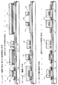
図1において、基板101には、無アルカリガラス基板や石英基板を使用することが望ましい。その他にもシリコン基板や金属基板の表面に絶縁膜を形成したものを基板としても良い。そして、基板101のTFTが形成される表面には、酸化シリコン膜、窒化シリコン膜、または窒酸化シリコン膜からなる下地膜102をプラズマCVD法やスパッタ法で100〜400nmの厚さに形成した。例えば下地膜102として、窒化シリコン膜102を25〜100nm、ここでは50nmの厚さに、酸化シリコン膜103を50〜300nm、ここでは150nmの厚さとした2層構造で形成すると良い。下地膜102は基板からの不純物汚染を防ぐために設けられるものであり、石英基板を用いた場合には必ずしも設けなくても良い。次に下地膜102の上に20〜100nmの厚さの、非晶質シリコン膜を公知の成膜法で形成した。非晶質シリコン膜は含有水素量にもよるが、好ましくは400〜550℃で数時間加熱して脱水素処理を行い、含有水素量を5atomic%以下として結晶化の工程を行うことが望ましい。また、非晶質シリコン膜をスパッタ法や蒸着法などの他の作製方法で形成しても良いが、膜中に含まれる酸素、窒素などの不純物元素を十分低減させておくことが望ましい。ここでは、下地膜と非晶質シリコン膜とは、同じ成膜法で形成することが可能であるので両者を連続形成しても良い。下地膜を形成後、一旦大気雰囲気にさらされないようにすることで表面の汚染を防ぐことが可能となり、作製されるTFTの特性バラツキを低減させることができる。非晶質シリコン膜から結晶質シリコン膜を形成する工程は、公知のレーザー結晶化技術または熱結晶化の技術を用いれば良い。また、シリコンの結晶化を助長する触媒元素を用いて熱結晶化の方法で結晶質シリコン膜を作製しても良い。その他に、微結晶シリコン膜を用いても良いし、結晶質シリコン膜を直接堆積成膜しても良い。さらに、単結晶シリコンを基板上に貼りあわせるSOI(Silicon On Insulators)の公知技術を使用して結晶質シリコン膜を形成しても良い。こうして形成された結晶質シリコン膜の不要な部分をエッチング除去して、島状半導体層104〜106を形成した。結晶質シリコン膜のnチャネル型TFTが作製される領域には、しきい値電圧を制御するため、あらかじめ1×10¹⁵〜5×1017cm-3程度の濃度でボロン(B)を添加しておいても良い。次に、島状半導体層104〜106を覆って、酸化シリコン、窒酸化シリコン、または窒化シリコンを主成分とするゲート絶縁膜107を形成した。ゲート絶縁膜107は、10〜200nm、好ましくは50〜150nmの厚さに形成すれば良い。例えば、プラズマCVD法でN2OとSiH4を原料とした窒化酸化シリコン膜を75nm形成し、その後、酸素雰囲気中または酸素と塩酸の混合雰囲気中、800〜1000℃で熱酸化して115nmのゲート絶縁膜としても良い(図1(A))。
【0020】
(第1の低濃度不純物領域の形成)
駆動回路のnチャネル型TFTに、LDD領域となる低濃度不純物領域を形成するために、島状半導体層104、106の全面と、島状半導体層105のチャネル形成領域をレジスト膜でマスク108〜111を形成した。このとき、島状半導体層の周辺の配線を形成する領域にもレジストマスクを形成しておいても良い。そして、n型を付与する不純物元素を添加して低濃度不純物領域を形成した。ここではフォスフィン(PH3)を用いたイオンドープ法でリン(P)を添加した。この工程では、ゲート絶縁膜107を通してその下の半導体層にリンを添加した。添加するリン濃度は、1×10¹⁶〜1×10¹⁹atoms/cm3の範囲にするのが好ましく、ここでは1×1018atoms/cm3とした。そして、島状半導体層105にリンが添加された第1の低濃度不純物領域112、113が形成された。
この第1の低濃度不純物領域はnチャネル型TFTにおいてLDD領域を形成するためのものであり、後にゲート電極との位置関係により、ゲート電極と重ならない第2の不純物領域と、ゲート電極と重なる第3の不純物領域とに区別される。
【0021】
その後、窒素雰囲気中で400〜900℃、好ましくは550〜800℃で1〜12時間の熱処理を行ない、この工程で添加されたn型を付与する不純物元素を活性化する工程を行なった(図1(B))。
【0022】
(ゲート電極用および配線用導電膜の形成)
第1の導電膜114を、タンタル(Ta)、チタン(Ti)、モリブデン(Mo)、タングステン(W)から選ばれた元素を主成分とする導電性材料で10〜100nmの厚さに形成した。第1の導電層には、窒化タンタル(TaN)や窒化タングステン(WN)を用いることが望ましい。また、図示しないが、第1の導電膜の下にシリコン膜を2〜20nm程度の厚さで形成しておいても良い。さらに、第1の導電膜114上に第2の導電膜115をTa、Ti、Mo、Wから選ばれた元素を主成分とする導電性材料で、100〜400nmの厚さに形成した。例えば、Taを200nmの厚さに形成すれば良い(図1(C))。
【0023】
第2の導電膜115をTa膜を用いる場合には、スパッタ法で形成することが可能である。Ta膜はスパッタガスにArを用いる。また、これらのスパッタガス中に適量のXeやKrを加えておくと、形成する膜の内部応力を緩和して膜の剥離を防止することができる。α相のTa膜の抵抗率は20μΩcm程度でありゲート電極に使用することができるが、β相のTa膜の抵抗率は180μΩcm程度でありゲート電極とするには不向きである。しかし、TaN膜はα相に近い結晶構造を持つので、この上にTa膜を形成すればα相のTa膜が容易に得られる。
従って、第1の導電膜114を10〜50nmの厚さでTaN膜で形成しておいても良い。Ta膜は抵抗率を10〜50μΩcmの範囲ですることが好ましい。
【0024】
その他、第2の導電膜をW膜で形成する場合には、Wをターゲットとしたスパッタ法で、アルゴン(Ar)ガスと窒素(N2)ガスを導入して第1の導電膜114を窒化タングステン(WN)膜で形成し、第2の導電膜115をArガスのスパッタでW膜で形成する。また、W膜を6フッ化タングステン(WF6)を用いて熱CVD法で形成することも可能である。いずれにしてもゲート電極として使用するためには低抵抗化を図る必要があり、W膜の抵抗率を20μΩcm以下にすることが望ましい。W膜は結晶粒を大きくすることで低抵抗率化を図ることができるが、W膜中に酸素などの不純物元素が多い場合には結晶化が阻害され高抵抗化する。このことより、スパッタ法による場合、純度99.9999%のWターゲットを用い、さらに成膜時に気相中からの不純物の混入がないように十分配慮してW膜を形成することにより、抵抗率9〜20μΩcmを実現することができる。
【0025】
(ゲート電極(p−ch)、配線電極の形成と第5の不純物領域の形成)
レジストマスク116〜119を形成し、第1の導電膜と第2の導電膜の一部をエッチング除去して、pチャネル型TFTのゲート電極120、ゲート配線122、123を形成した。nチャネル型TFTのゲート電極は後の工程で形成するため、第1の導電膜と第2の導電膜が半導体層105、106上の全面で残るようにした。そして、レジストマスク116〜119をそのまま残してマスクとし、pチャネル型TFTが形成される半導体層104の一部に、p型を付与する不純物元素を添加するの工程を行った。ここではボロンをその不純物元素として、ジボラン(B2H6)を用いてイオンドープ法で添加した。ここでは2×10²⁰atoms/cm3の濃度にボロンを添加した。そして、図2(A)に示すようにボロンが高濃度に添加された第5の不純物領域125、126が形成された。また、この工程において、レジストマスク116〜119を使用してゲート絶縁膜107の一部をエッチング除去して、島状半導体層104の一部を露出させた後、p型を付与する不純物元素を添加するの工程を行っても良い。
【0026】
(ゲート電極(n−ch)の形成)
レジストマスク127〜130を形成し、nチャネル型TFTのゲート電極131、132を形成した。このときゲート電極131は低濃度不純物領域112、113と一部が重なるように形成した(図2(B))。
【0027】
(第1の不純物領域の形成)
レジストマスク134〜136を形成し、nチャネル型TFTにおいて、ソース領域またはドレイン領域として機能する第1の不純物領域を形成する工程を行なった。レジストマスク136はnチャネル型TFTのゲート電極132を覆う形で形成された。これは、画素部のnチャネル型TFTにおいて、オフセットLDD領域となる第4の不純物領域を形成するために設けた。そして、n型を付与する不純物元素を添加して第1の不純物領域139〜143を形成した。ここでも、フォスフィン(PH3)を用いたイオンドープ法で行い、この領域のリンの濃度は1×10¹⁹〜1×10²¹atoms/cm3とするのが好ましく、ここでは1×1020atoms/cm3とした。また、同時に島状半導体層104のボロンが添加されている領域125、126の一部にもリンが添加された領域137、138が形成された(図2(C))。
【0028】
(第2の低濃度不純物領域の形成)
画素部のnチャネル型TFTの、LDD領域となる低濃度不純物領域(本発明では第4の不純物領域と記す)を島状半導体層106に形成するためにn型を付与する不純物元素を添加する工程を行った。添加するリン濃度は、第1の低濃度不純物領域と同程度かそれより少なくするのが好ましく、ここでは2×10¹⁷atoms/cm3とした。そして、島状半導体層にリンが添加された第2の低濃度不純物領域144〜147を形成した(図3(A))。
【0029】
(熱活性化の工程)
ゲート絶縁膜、ゲート電極上の全面に(島状半導体層104〜106の一部が露出されている場合にはその上面にも)第1の層間絶縁膜148を形成した。第1の層間絶縁膜は窒化シリコン膜、酸化シリコン膜、または窒酸化シリコン膜で形成すれば良い。また、窒化シリコン膜と、酸化シリコン膜または窒酸化シリコン膜の2層構造としても良い(図示せず)。いずれにしても、第1の層間絶縁膜は500〜1000nmの厚さとなるように形成すれば良い。その後、それぞれの濃度で添加されたn型またはp型を付与する不純物元素を活性化するための熱処理の工程を行った。この工程は、電気加熱炉を用いた熱アニール法や、ハロゲンランプを用いたラピットサーマルアニール法(RTA法)で行うことができる。ここでは熱アニール法で活性化の工程を行った。加熱処理は、窒素雰囲気中において300〜700℃、好ましくは350〜550℃、例えば525℃、2時間の熱処理を行った。この処理で、半導体層の結晶化の工程でシリコンの結晶化を助長する触媒元素を用いて熱結晶化の方法で結晶質シリコン膜を作製した場合には、その触媒元素をリンを添加した領域に偏析させるゲッタリング効果が同時に得られ、チャネル形成領域から触媒元素を除去することができた。さらに、3〜100%の水素を含む雰囲気中で、300〜450℃で1〜12時間の熱処理を行い、島状半導体層を水素化する工程を行った。この工程は、プラズマ水素化法を用い、プラズマ化されることにより生成された水素雰囲気中で200〜450℃の熱処理を行っても良い(図3(B))。
【0030】
(ソース・ドレイン配線、層間絶縁膜の形成)
第1の層間絶縁膜148にはその後、それぞれのTFTのソース領域と、ドレイン領域に達するコンタクトホールが形成された。そして、ソース配線149、150、151と、ドレイン配線152、153を形成した。図示していないが、本実施例ではこの電極を、Ti膜を100nm、Tiを含むAl膜300nm、Ti膜150nmをスパッタ法で連続して形成した3層構造の電極として用いた。そして、第1の層間絶縁膜、ソース配線、ドレイン配線、およびそれぞれの配線電極上にパッシベーション膜154を形成した。パッシベーション膜154は、窒化シリコン膜、酸化シリコン膜、または窒酸化シリコン膜で50〜500nmの厚さで形成した。その後、この状態で水素化処理を行うとTFTの特性向上に対して好ましい結果が得られた。例えば、3〜100%の水素を含む雰囲気中で、300〜450℃で1〜12時間の熱処理を行うと良く、あるいはプラズマ水素化法を用い、プラズマ化されることにより生成された水素雰囲気中で200〜450℃の熱処理を行っても同様の効果が得られた。その後、有機樹脂からなる第2の層間絶縁膜155を約1000nmの厚さに形成した。有機樹脂膜としては、ポリイミド、アクリル、ポリイミドアミド等を使用することができる。
有機樹脂膜を用いることの利点は、成膜方法が簡単である点や、比誘電率が低いので、寄生容量を低減できる点、平坦性に優れる点などが上げられる。なお上述した以外の有機樹脂膜を用いることもできる。ここでは、基板に塗布後、熱重合するタイプのポリイミドを用い、300℃で焼成して形成した。
【0031】
(保持容量、画素電極の形成)
画素部の第2の層間絶縁膜上に遮光膜156を形成した。遮光膜156はアルミニウム(Al)、チタン(Ti)、タンタル(Ta)から選ばれた元素を主成分とする膜で100〜300nmの厚さに形成した。そしてこの部分に保持容量を形成する目的で、遮光膜156上に誘電体膜157を50〜200nmの厚さで形成した。この誘電体膜157は、陽極酸化法を用いて遮光膜156の表面に形成された酸化膜を用いても良い。その他にも酸化シリコン膜、窒化シリコン膜、窒酸化シリコン膜やDLC(Diamond like carbon)膜やポリイミド膜を用いても良い。しかしながら、例えばポリイミドの比誘電率3〜4に対して陽極酸化法で作製された酸化Alの比誘電率は7〜9であるので、少ない面積で大きな容量を形成する目的には後者の方が非常に適していた。
【0032】
具体的には、Al膜上に陽極酸化法で酸化Al膜を形成し、その上に0.785mm2の電極を作製して容量を測定した結果、酸化Al膜の厚さが50nmのとき1100pF、100nmのとき630pFが得られた。この容量の値はポリイミドを同様な厚さで形成した場合の2〜3倍の値であった。液晶表示装置の画素部に設ける保持容量は画素の大きさに依存するが100〜300fFの容量が必要であり、酸化Al膜を用いて保持容量を形成するとこの容量を得るために必要な面積をポリイミドを用いた場合の1/3程度にすることができた。
【0033】
そして、第2の層間絶縁膜155に設けられた開孔部159と、パッシベーション膜154に設けられた開孔部158で、ドレイン配線153に達するコンタクトホールを形成し、画素電極160を形成した。画素電極160は、透過型液晶表示装置とする場合には透明導電膜を用い、反射型の液晶表示装置とする場合には金属膜を用いれば良い。ここでは透過型の液晶表示装置とするために、酸化インジウム・スズ(ITO)膜を100nmの厚さにスパッタ法で形成した。画素電極160は、誘電体膜157を介して遮光膜156上まで延在して形成され、画素電極160が遮光膜156と重なる領域で保持容量184が形成された(図3(C))。
【0034】
以上の工程で、画素部にはnチャネル型TFT183が形成され、周辺に設けられる駆動回路にはpチャネル型TFT181、nチャネル型TFT182が同一基板上に形成されたアクティブマトリクス基板が作製された。
【0035】
駆動回路のpチャネル型TFT181には、チャネル形成領域161、ソースまたはドレイン領域として機能する第5の不純物領域162、163が形成された。そして、第5の不純物領域162はソース領域として、第5の不純物領域163はドレイン領域となった。また、nチャネル型TFT182には、チャネル形成領域164、第1の不純物領域165、166、第1の低濃度不純物領域からゲート電極と重なり、LDD領域として機能する第3の不純物領域167、168が形成された。第1の不純物領域165はソース領域として、第1の不純物領域166はドレイン領域として機能した。
【0036】
また、画素部のnチャネル型TFT183には、チャネル形成領域169、170、ソースまたはドレイン領域として機能する第1の不純物領域171、172、173、第2の低濃度不純物領域からゲート電極と重ならないLDD領域として機能する第4の不純物領域174〜177が形成された。
【0037】
本発明は、画素部および駆動回路のそれぞれのnチャネル型TFTの動作環境を考慮して、LDD領域となる第2の不純物領域、第3の不純物領域、第4の不純物領域のチャネル長方向の長さを同一基板上で異ならせ、それぞれの回路を構成するTFTに対して、最適な形状を作り込むことができた。nチャネル型TFT182は駆動電圧が10V程度のロジック回路などに適している。チャネル長3〜7μmに対してゲート電極とオーバーラップしたLDD領域(第3の不純物領域)の長さ(Lov)は0.5〜3.0μm、代表的には1.5μmとすれば良い。また、画素部のnチャネル型TFT183はマルチゲート構造であるが、極性反転して駆動されるために、ソース側およびドレイン側の両方にゲート電極と重ならないLDD領域となる第4の不純物領域174〜177が設けられている。この領域の長さ(Loff)は0.5〜3.5μm、代表的には2.0μmとすれば良い。
【0038】
以上の様に本発明は、画素部および駆動回路がそれぞれ要求する仕様に応じて各回路を構成するTFTの構造を最適化することで、半導体装置の動作性能と信頼性を向上させることを可能とすることができる。具体的には、各回路仕様に応じてnチャネル型TFTのLDD領域の設計をそれぞれ異ならせ、ゲート電極とオーバーラップするLDD領域またはオーバーラップしないLDD領域を適宣設けることによって、同一の基板上にホットキャリア劣化の対策を重視したTFT構造と、低オフ電流値を重視したTFT構造とを実現することができる。
【0039】
[実施形態2]
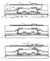
アクティブマトリクス基板の画素部のnチャネル型TFTに接続される保持容量の他の構成について説明する。図4は実施形態1と同様にして作製されたアクティブマトリクス基板の画素部の断面構造図を示す。
【0040】
基板401上に下地膜402、403が形成され、島状半導体層404には第1の不純物領域と第4の不純物領域が形成されている。ゲート絶縁膜405上にはゲート電極406が形成され、第1の層間絶縁膜407上にはソース配線408、ドレイン配線409が形成されている。そして、パッシベーション膜410、第2の層間絶縁膜411上に遮光膜412、画素電極418が形成されている。
【0041】
nチャネル型TFT420に接続される保持容量421は、第2の層間絶縁膜411上に形成された遮光膜412と、その上に形成された誘電体膜413と、画素電極418とから形成されている。また、第2の層間絶縁膜の開口が形成される領域には絶縁体のスペーサー414が設けられ、パッシベーション膜410に設けられた開孔415、第2の層間絶縁膜411に設けられた開孔416、スペーサー414に設けられた開口417で、画素電極418がドレイン配線409に接続されている。このようにスペーサー414を設けることにより、遮光膜と画素電極との間で発生するショートを防止することができる。保持容量421は遮光膜412、誘電体膜413、画素電極418が重なる部分で形成されている。
【0042】
[実施形態3]
図5は画素部のnチャネル型TFTに接続される保持容量の他の構成について示している。図5(A)は実施形態1と同様にして作製された画素部のnチャネル型TFTである。基板501上に下地膜502、503が形成され、島状半導体層504には第1の不純物領域と第4の不純物領域が形成されている。ゲート絶縁膜505上にはゲート電極506が形成され、第1の層間絶縁膜507上にはソース配線508、ドレイン配線509が形成されている。さらに、パッシベーション膜510、第2の層間絶縁膜上に遮光膜512、有機樹脂で形成したスペーサー513を形成した。その後、図5(B)のように陽極酸化法で遮光膜の表面に誘電体膜514を形成した。そして、図5(C)のようにパッシベーション膜510に設けられた開孔515、第2の層間絶縁膜511に設けられた開孔516、スペーサー513に設けられた開口517で、画素電極518がドレイン配線509に接続されている。保持容量521は遮光膜512、誘電体膜514、画素電極518が重なる部分で形成されている。このようにスペーサー513を設けることにより、遮光膜と画素電極との間で発生するショートを防止することができ、また、遮光膜512の表面に誘電体膜514を形成するときに端部への回り込みを防止することができる。
【0043】
【実施例】
[実施例1]
本実施例では本発明を用いて、画素部とその駆動回路を同一基板上に作製する一例を図6〜8を用いて説明する。本明細書ではこのような基板を便宜上アクティブマトリックス基板と呼ぶ。最初に、基板601上に下地膜として窒酸化シリコン膜602aを50〜500nm、代表的には100nmの厚さに形成した。
窒酸化シリコン膜602aは、SiH4とN2OとNH3から作製されるものであり、含有する窒素濃度を25atomic%以上50atomic%未満となるようにした。
その後、窒素雰囲気中で450〜650℃の熱処理を施し、窒酸化シリコン膜602aを緻密化した。さらに窒酸化シリコン膜602bを100〜500nm、代表的には200nmの厚さに形成し、連続して非晶質半導体膜(図示せず)を20〜80nmの厚さに形成した。そして公知の結晶化の方法により結晶質シリコン膜を形成した(図示せず)。結晶質シリコン膜の不要な部分はエッチング除去され、島状の結晶質半導体膜603〜606が形成され、さらにゲート絶縁膜607が形成された。ゲート絶縁膜607は、SiH4とN2Oとから作製される窒酸化シリコン膜であり、ここでは10〜200nm、好ましくは50〜150nmの厚さで形成した(図6(A))。
【0044】
次に、島状半導体層603、606の全面と、島状半導体層604、605のチャネル形成領域を覆うレジストマスク608〜611を形成した。そして、フォスフィン(PH3)を用いたイオンドープ法でn型を付与する不純物元素を添加して第1の低濃度不純物領域を形成した。この工程では、ゲート絶縁膜607を通してその下の島状半導体層にリンを添加するために、加速電圧は65keVに設定した。島状半導体に添加されるリンの濃度は、1×10¹⁶〜1×10¹⁹atoms/cm3の範囲にするのが好ましく、ここでは1×1018atoms/cm3とした。そして、リンが添加された第1の低濃度不純物領域612〜615を形成した(図6(B))。
【0045】
第1の導電膜616を、スパッタ法により窒化タンタル(TaN)または窒化タングステン(WN)で形成した。また、図示しないが、第1の導電膜の下にシリコン膜を2〜20nm程度の厚さで形成しておいても良い。続いて、アルミニウム(Al)や銅(Cu)を主成分とする第3の導電膜617を、100〜300nmの厚さに形成した(図6(C))。そして、入出力端子から駆動回路の入出力までの配線の一部とするために、第3の導電膜をエッチングして配線618を形成した。例えば、第3の導電膜にAlを用いれば、リン酸溶液により下地TaNと選択性良くエッチングすることができた。さらに、第1の導電層616と配線618上に第2の導電膜619をTa、Ti、Mo、Wから選ばれた元素を主成分とする導電性材料で、100〜400nmの厚さに形成した。例えば、Taを200nmの厚さに形成すれば良い(図6(D))。
【0046】
次に、レジストマスク620〜625を形成し、第1の導電膜と第2の導電膜の一部をエッチング除去して、入出力端子から駆動回路の入出力までの配線626、pチャネル型TFTのゲート電極627と、ゲート配線630を形成した。
TaN膜とTa膜のエッチングはCF4とO2の混合ガスにより行うことができた。そして、レジストマスク620〜625をそのまま残して、pチャネル型TFTが形成される島状半導体層603の一部に、p型を付与する不純物元素を添加する工程を行った。ここではボロンをその不純物元素として、ジボラン(B2H6)を用いてイオンドープ法で添加した。この領域のボロン濃度は2×10²⁰atoms/cm3とした。そして、図7(A)に示すようにボロンが高濃度に添加された第5の不純物領域633、634が形成された。
【0047】
入出力端子から駆動回路の入出力までの配線626は第3の導電層の回りを第1の導電層と第2の導電層とで覆うようにして形成されている。
【0048】
図7(A)で設けられたレジストマスクを除去した後、新たにレジストマスク635〜640を形成した。これはnチャネル型TFTのゲート電極を形成するためのものであり、ドライエッチング法によりnチャネル型TFTのゲート電極641〜643が形成された。このときゲート電極641、642は第1の低濃度不純物領域612〜615の一部と重なるように形成された(図7(B))。
【0049】
このようにゲート電極627、641〜643は第1の導電膜と第2の導電膜とから形成される。
【0050】
そして、新たなレジストマスク645〜649を形成した。レジストマスク647、649はnチャネル型TFTのゲート電極642、643と第2の不純物領域の一部を覆う形で形成された。そして、n型を付与する不純物元素を添加して第1の不純物領域を形成する工程を行い、nチャネル型TFTが形成される島状半導体層に第1の不純物領域650〜655が形成された(図7(C))。
【0051】
画素部のnチャネル型TFTのLDD領域となる第2の低濃度不純物領域を島状半導体層606に形成するためにn型を付与する不純物元素を添加する工程を行った。添加するリン濃度は、第2および第3の不純物領域と同程度かそれより少なくするのが好ましく、ここでは2×10¹⁷atoms/cm3とし、ゲート電極をマスクとして自己整合的に第2の低濃度不純物領域656〜658を形成した(図8(A))。
【0052】
そして、第1の層間絶縁膜659をプラズマCVD法でSiH4、N2O、NH3を原料とした窒酸化シリコン膜で形成した。この窒酸化シリコン膜中の含有水素濃度は1〜30atomic%となるように形成することが望ましかった。その後、この状態で窒素雰囲気中で400〜800℃、1〜12時間、例えば525℃で8時間の加熱処理を行った。この工程により添加されたn型及びp型を付与する不純物元素を活性化させることができた。この熱処理の後に水素化の工程を行なった。こでは3〜100%の水素雰囲気中で300〜500℃、好ましくは350〜450℃で2〜12時間の水素化処理の工程を行うと良い。または、200〜500℃、好ましくは300〜450℃の基板温度でプラズマ化させることによってできた水素で水素化処理をしても良い(図8(B))。
【0053】
その後、第1の絶縁膜659は所定のレジストマスクを形成して、エッチング処理によりそれぞれのTFTのソース領域と、ドレイン領域に達するコンタクトホールを形成した。そして、ソース配線660、663、664、666とドレイン配線661、662、665、657を形成した。図示していないが、本実施例ではこの電極を、Ti膜を100nm、Tiを含むAl膜300nm、Ti膜150nmをスパッタ法で連続して形成した3層構造の電極として用いた。
【0054】
そしてこの上に、パッシベーション膜670を形成した。パッシベーション膜670はプラズマCVD法でSiH4、N2O、NH3から形成される窒酸化シリコン膜、またはSiH4、N2、NH3から作製される窒化シリコン膜で形成すれば良い。まず、膜の形成に先立ってN2O、N2、NH3等を導入してプラズマ水素化処理により水素化の工程を行なった。プラズマ化されることにより気相中で生成された水素は第1の層間絶縁膜中に供給され、基板を200〜400℃に加熱しておけば、その水素を下層側にも拡散して半導体層を水素化することができた。このパッシベーション膜の作製条件は特に限定されるものではないが、緻密な膜とすることが望ましい。また、パッシベーション膜を形成した後に、水素化の工程を水素または窒素を含む雰囲気中で300〜550℃の加熱処理を1〜12時間の加熱処理により行っても良い。
【0055】
その後、有機樹脂からなる第2の層間絶縁膜671を約1000nmの厚さに形成した。有機樹脂膜としては、ポリイミド、アクリル、ポリイミドアミド等を使用することができる。有機樹脂膜を用いることの利点は、成膜方法が簡単である点や、比誘電率が低いので、寄生容量を低減できる点、平坦性に優れる点などが上げられる。なお上述した以外の有機樹脂膜を用いることもできる。ここでは、基板に塗布後、熱重合するタイプのポリイミドを用い、300℃で焼成して形成した。
【0056】
第2の層間絶縁膜上に窒酸化シリコン膜や酸化シリコン膜などで絶縁膜644を5〜50nm形成しておくと、この上に形成する遮光膜の密着性を高めることができた。また、有機樹脂で形成した第2の層間絶縁膜表面をCF4プラズマで処理して表面改質すると、この上に形成する膜の密着性を向上させることができた。そしてスパッタ法や真空蒸着法でAl膜を形成しエッチング処理して遮光膜672とした。この遮光膜672は陽極酸化法によってその表面に50〜200nmの酸化膜を形成した。陽極酸化は、まず十分にアルカリイオン濃度の小さい酒石酸エチレングリコール溶液を作製した。酒石酸の濃度としては、0.1〜10%、好ましくは3%とし、これに1〜20%のアンモニア水を加え、pHが7±0.5となるように調節した。この溶液中に陰極となる白金電極を設け、遮光膜672が形成されている基板を溶液に浸した。そして、遮光膜672を陽極として、直流電流を2mA一定となるようにした。溶液中の陰極と陽極との間の電圧は酸化膜の成長に従い時間と共に変化するが、電流が一定となるように電圧を調整し、150Vとなったところで電圧を一定として、その後電流が0.1mAになるまで保持した。このようにして遮光膜672の表面には厚さ50〜200nmの酸化Al膜673を形成することができた。尚、ここで示した陽極酸化法に係わる数値は一例にすぎず、作製する素子の大きさ等によって当然最適値は変化しうるものである。そして、絶縁膜644、第2の層間絶縁膜671、パッシベーション膜670に設けられた開孔部でドレイン配線667に達するコンタクトホールを形成し、画素電極676を形成した。画素電極676は、透過型液晶表示装置とする場合には透明導電膜を用い、反射型の液晶表示装置とする場合には金属膜を用いれば良かった。ここでは透過型の液晶表示装置とするために、酸化インジウム・スズ(ITO)膜を100nmの厚さにスパッタ法で形成した。
画素電極676は、酸化Al膜673を介して遮光膜672上まで延在して形成され、画素電極676が遮光膜672と重なる領域で保持容量700が形成された。以上の工程で、画素部とその周辺に設けられる駆動回路のTFTが同一基板上に形成されたアクティブマトリクス基板が作製された(図8(C))。
【0057】
pチャネル型TFT701は自己整合的(セルフアライン)に形成され、nチャネル型TFT702〜704は非自己整合的(ノンセルフアライン)に形成された。駆動回路のpチャネル型TFT701には、チャネル形成領域677、第5の不純物領域678、679が形成された。第5の不純物領域678はソース領域として、第5の不純物領域679はドレイン領域となった。
一方、nチャネル型TFT702には、チャネル形成領域680、ソース領域となる第1の不純物領域681、ドレイン領域となる第1の不純物領域682、第1の低濃度不純物領域からゲート電極と重なりLDD領域となる第3の不純物領域683、684が形成された。このnチャネル型TFTはシフトレジスタ回路やバッファ回路に適している。
また、nチャネル型TFT703には、チャネル形成領域685、ソース領域となる第1の不純物領域686、ドレイン領域となる第1の不純物領域687、第1の低濃度不純物領域からゲート電極と重なりLDD領域となる第3の不純物領域688a、689aとゲート電極と重ならないLDD領域となる第2の不純物領域688b、689bが形成された。このようなnチャネル型TFTは、アナログスイッチが形成されるサンプリング回路に適していた。
画素部のnチャネル型TFT704には、チャネル形成領域690、691、第1の不純物領域692、696、第2の低濃度不純物領域からゲート電極と重ならないLDD領域となる第4の不純物領域693〜695が形成された。
【0058】
以上の様に本発明は、画素部および駆動回路がそれぞれ要求する仕様に応じて各回路を構成するTFTの構造を最適化することで、半導体装置の動作性能と信頼性を向上させることを可能とすることができる。例えば、駆動回路のnチャネル型TFT702にはゲート電極と重なるLDD領域(GOLD)が設けられている。このようなLDDを設けることにより、キンク効果やホットエレクトロン効果などによる特性の変動を防ぐことができ、シフトレジスタや、特にバッファ回路などに適している。また、nチャネル型TFT703にはゲート絶縁膜を介してゲート電極と重なるLDD領域(GOLD)688a、689a、ゲート電極と重ならないLDD領域688b、689bが形成され、オフ電流値を下げる目的とホットキャリア効果によるTFTの劣化を防ぐ上で効果がある。また、画素部に設けるnチャネル型TFTはゲート電極と重ならないLDD領域693〜695のみを設ける構造とし、主にオフ電流値を下げてスイッチング動作を確実なものとすると共に、消費電力を低減させる上で効果的である。
【0059】
[実施例2]
本実例では、アクティブマトリクス基板から、アクティブマトリクス型液晶表示装置を作製する工程を説明する。図9に示すように、図8(C)の状態の基板に対し、配向膜901を形成する。通常液晶表示素子の配向膜にはポリイミド樹脂が多く用いられている。対向側の基板902には、透明導電膜903と、配向膜904とを形成した。配向膜は形成された後、ラビング処理を施して液晶分子がある一定のプレチルト角を持って平行配向するようにした。そして、画素部と、駆動回路が形成されたアクティブマトリクス基板と対向基板とを、公知のセル組み工程によってシール材やスペーサ(共に図示せず)などを介して貼りあわせる。その後、両基板の間に液晶材料905を注入し、封止剤(図示せず)によって完全に封止した。液晶材料にはTN液晶の他に反強誘電性液晶(Antiferroelectric Liquid Crystal)、しきい値なし反強誘電性液晶などを適用できる。このようにして図9に示すアクティブマトリクス型液晶表示装置が完成した。
【0060】
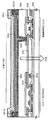
次に、このアクティブマトリクス型液晶表示装置の構成を、図10の斜視図および図11の上面図を用いて説明する。尚、図10と図11は、図6〜図8の断面構造図と対応付けるため、共通の符号を用いている。アクティブマトリクス基板は、ガラス基板601上に形成された、画素部1001と、走査(ゲート)線駆動回路1002と、信号(ソース)線駆動回路1003で構成される。画素部にはnチャネル型TFT704が形成され、周辺に設けられる駆動回路はCMOS回路を基本として構成されている。走査(ゲート)線駆動回路1002と、信号(ソース)線駆動回路1003はそれぞれゲート配線643とソース配線666で画素部1001に接続されている。また、FPC1031が接続された外部入出力端子1034から駆動回路の入出力端子までの配線626、668が設けられている。
【0061】
図11は画素部1001の一部分を示す上面図である。ここで図11(A)は半導体層、ゲート電極、ソース配線の重ねあわせを示す上面図であり、同図(B)はその上に形成される遮光膜、画素電極の重ねあわせを示す上面図である。ゲート電極643は、図示されていないゲート絶縁膜を介してその下の半導体層606と交差している。図示はしていないが、半導体層606には、ソース領域、ドレイン領域、第4の不純物領域が形成されている。また、画素TFTの上には遮光膜672と、誘電体膜(図示せず)と、各画素ごとに設けられる画素電極676が形成され、遮光膜672と画素電極676とが誘電体膜を介して重なる領域で保持容量700が形成される。遮光膜を形成するAl膜の表面を酸化して容量部を形成するための誘電体膜としたことで、必要な容量を形成するための面積を少なくすることが可能であり、さらに、本実施例のように画素部のnチャネル型TFT上に形成される遮光膜を保持容量の一方の電極とすることで、アクティブマトリクス型液晶表示装置の画像表示部の開口率を向上させることができた。
また、図11で示すA―A'に沿った断面構造は、図8に示す画素部のA―A'断面図に対応している。
【0062】
[実施例3]
図12に、画素部のTFTに設けられる保持容量の接続方法の他の構成例を示す。図12は実施形態1と同様にして作製されたアクティブマトリクス基板の画素部の断面構造図を示す。基板1201上に下地膜1202、1203が形成され、島状半導体層1204には第1の不純物領域と第4の不純物領域が形成されている。ゲート絶縁膜1205上にはゲート電極1206が形成され、第1の層間絶縁膜1207上にはソース配線1208、ドレイン配線1209が形成されている。さらに、パッシベーション膜1211、第2の層間絶縁膜1212上に遮光膜1213が形成されている。
【0063】
図12(A)において、nチャネル型TFTに接続される保持容量1240は、第2の層間絶縁膜1212上に形成された遮光膜1213と、その上に形成された誘電体膜1214と、画素電極1215とから形成されている。そして、保持容量1240の一方の電極である画素電極1215は、パッシベーション膜1211と第2の層間絶縁膜1212に設けられた開孔1260でドレイン配線1209に接続されている。また、他方の電極である遮光膜は、パッシベーション膜1211と第2の層間絶縁膜1212に設けられた開孔1261で、第1の層間絶縁膜1207上に形成された配線電極1210と接続されている。また、図12(B)では画素電極1215と同じ材料で形成された配線1216と、遮光膜1213が誘電体膜1214を介して接続部1251で静電結合して、パッシベーション膜1211と第2の層間絶縁膜1212に設けられた開孔1261で第1の層間絶縁膜1207上に形成された配線電極1210と接続することも可能である。また、図12(B)では、遮光膜1213が誘電体膜1214、配向膜1217、液晶1218、対向基板側の配向膜1219を介して共通電極1220と静電的に結合させることも可能である。
【0064】
[実施例4]
図13は、実施例1で示したアクティブマトリクス基板の回路構成の一例を示す。本実施例のアクティブマトリクス基板は、ソース信号線側駆動回路1301、ゲート信号線側駆動回路(A)1307、ゲート信号線側駆動回路(B)1311、プリチャージ回路1312、画素部1306を有している。ソース信号線側駆動回路1301は、シフトレジスタ回路1302、レベルシフタ回路1303、バッファ回路1304、サンプリング回路1305を備えている。また、ゲート信号線側駆動回路(A)1307は、シフトレジスタ回路1308、レベルシフタ回路1309、バッファ回路1310を備えている。ゲート信号線側駆動回路(B)1311も同様な構成である。
【0065】
ここで、それぞれの回路の駆動電圧の一例を示すと、シフトレジスタ回路1302、1308は10〜16Vであり、レベルシフタ回路1303、1309、バッファ回路1304、1310、サンプリング回路1305、画素部1306は14〜16Vであった。サンプリング回路1305、画素部1306は印加される電圧の振幅であり、通常極性反転された電圧が交互に印加されていた。本発明は、nチャネル型TFTの駆動電圧を考慮して、LDD領域となる第2の不純物領域の長さを同一基板上で異ならしめることが容易であり、それぞれの回路を構成するTFTに対して、最適な形状を同一工程で作り込むことができた。
【0066】
図14(A)はシフトレジスタ回路のTFTの構成例を示している。シフトレジスタ回路のnチャネル型TFTはシングルゲート構造であり、チャネル形成領域204とゲート電極210とオーバーラップする第3の不純物領域(LDD領域)205、206が設けられている。その外側にはソース領域またはドレイン領域となる第1の不純物領域207、208が形成されている。この領域のチャネル長方向の長さは、チャネル長を3〜7μmとして、0.5〜3μmとすれば良い。このLDDの構成は、ホットキャリア劣化対策に有効であり、オフ領域の特性を重視しないシフトレジスタ回路などに適している。一方、pチャネル型TFTには、チャネル形成領域201、ゲート電極209の外側にソース領域またはドレイン領域となる第5の不純物領域202、203が形成されている。そして、各TFTのソースまたはドレイン領域とコンタクトを形成するソース配線211、212とドレイン配線213が形成されている。
【0067】
図14(B)はレベルシフタ回路、バッファ回路のTFTの構成例を示している。これらの回路のnチャネル型TFTはダブルゲート構造としてあるが、勿論シングルゲート構造としても問題ない。このnチャネル型TFTもチャネル形成領域204a、204b、ゲート電極210a、210bとオーバーラップする第3の不純物領域(LDD領域)205a、205b、206a、206bが設けられた構造である。このようなLDDを設けることにより、ドレイン近傍の高電界領域が緩和され、キンク効果やホットエレクトロン効果などによる特性の変動を防ぐことができる。その結果、バッファ回路の信頼性を高めることができる。また、pチャネル型TFTは図14(A)と同様な構成とする。
【0068】
図14(C)はサンプリング回路のTFTの構成例を示している。この回路のnチャネル型TFTはシングルゲート構造であるがチャネル形成領域の外側に、極性反転して駆動することに対応して、ソース側およびドレイン側の両方にゲート電極とオーバーラップするLDD領域となる第2の不純物領域205c、206cが設けられている。第2の不純物領域205cと206cの長さは、それぞれ等しくすることが好ましく、0.5〜3.0μmの範囲で形成すると良い。これらのLDD領域によりオフ電流値を下げる目的と、ホットキャリア効果によるTFTの劣化を防ぐ目的を同時に達成できる。また、pチャネル型TFTは図14(A)と同様な構成とする。
【0069】
また、図14(D)は、1.5〜5V程度の駆動電圧で高速動作させる駆動回路に適した構成で、nチャネル型TFTのソース領域207側には、ゲート電極210とオーバーラップしない第2の不純物領域205dが設けられ、ドレイン領域208側にはゲート電極210とオーバーラップする第3の不純物領域206dが設けられている。このようにして、寄生容量による動作周波数の低下を防ぐ構成となっている。
【0070】
[実施例5]
本実施例では、本発明に適用できる半導体層の作製方法について説明する。図15において基板1501はガラス基板、セラミクス基板、石英基板などを用いることができる。また、酸化シリコン膜や窒化シリコン膜などの絶縁膜を表面に形成したシリコン基板やステンレスに代表される金属基板を用いても良い。ガラス基板を用いる場合には、歪み点以下の温度で予め加熱処理しておくことが望ましい。例えば、コーニング社の#1737基板を用いる場合には、500〜650℃、好ましくは595〜645℃で1〜24時間の加熱処理をしておくと良い。
【0071】
そして、基板1501の主表面に、下地膜を形成した。下地膜の材質に特別な限定はないが、窒酸化シリコン膜1502で形成した。その他にも窒化シリコン膜、酸化シリコン膜、窒酸化シリコン膜、酸化タンタル膜から選ばれた一層もしくは複数の層で形成することも可能である。窒酸化シリコン膜を用いる場合には、20〜100nm、代表的には50nmの厚さに形成すれば良い。また、10〜100nmの窒化シリコン膜上に窒酸化シリコン膜を50〜500nm、代表的には50〜200nmの厚さに形成しても良い。そしてこの上に非晶質半導体層1503を形成した。これはプラズマCVD法、減圧CVD法、スパッタ法などの成膜法で形成される非晶質半導体であれば良く、シリコン(Si)、ゲルマニウム(Ge)、またシリコンゲルマニウム合金、炭化シリコンがあり、その他にガリウム砒素などの化合物半導体材料を用いることができる。半導体層は10〜100nm、代表的には50nmの厚さとして形成した。また、下地膜1501と非晶質半導体層1503とをプラズマCVD法やスパッタ法で連続形成することも可能である。それぞれの層が形成された後、その表面が大気雰囲気に触れないことにより、その表面の汚染を防ぐことができる(図15(A))。
【0072】
次に結晶化の工程を行った。非晶質半導体層を結晶化する工程は、公知のレーザー結晶化技術または熱結晶化の技術を用いれば良い。また、プラズマCVD法で作製される非晶質半導体層には10〜40atomic%の割合で膜中に水素が含まれていて、結晶化の工程に先立って400〜500℃の熱処理の工程を行い水素を膜中から脱離させて含有水素量を5atomic%以下としておくことが望ましかった(図15(B))。そして、結晶性半導体層1504から島状の結晶性半導体層1505を形成し、さらにゲート絶縁膜1505を形成した。ゲート絶縁膜1505には、窒化シリコン膜、酸化シリコン膜、窒酸化シリコン膜、などの材料で形成すれば良い。ゲート絶縁膜1505の厚さは10〜1000nm、好ましくは50〜400nmとして形成すれば良い。以降の工程は実施例1に従うと本発明の半導体装置を形成することができる(図15(C))。
【0073】
図16は、基板1601の主表面に、窒酸化シリコン膜からなる下地膜1602を形成し、図15と同様にその表面に非晶質半導体層1603を形成した。非晶質半導体層の厚さは、10〜200nm、好ましくは30〜100nmに形成すれば良い。さらに、重量換算で10ppmの触媒元素を含む水溶液をスピンコート法で塗布して、触媒元素含有層1604を非晶質半導体層1603の全面に形成した。ここで使用可能な触媒元素は、ニッケル(Ni)の以外にも、ゲルマニウム(Ge)、鉄(Fe)、パラジウム(Pd)、スズ(Sn)、鉛(Pb)、コバルト(Co)、白金(Pt)、銅(Cu)、金(Au)、といった元素であった。非晶質半導体層の内部応力は、作製条件により一様に決まるものではなかった。しかし、結晶化の工程に先立って400〜600℃の熱処理の工程を行い水素を膜中から脱離させる必要があった(図16(A))。そして、500〜600℃で4〜12時間、例えば550℃で8時間の熱処理を行い、結晶質半導体層1605が形成された(図16(B))。
【0074】
次に、結晶化の工程で用いた触媒元素を結晶質半導体膜から除去するゲッタリングの工程を行った。このゲッタリングの工程により結晶質半導体膜中の触媒元素の濃度を1×10¹⁷atms/cm3以下、好ましくは1×1016atms/cm3にまで低減することができた。まず、結晶質半導体層1605の表面にマスク絶縁膜膜1606を150nmの厚さに形成し、パターニングにより開口部1607が設けられ、結晶質半導体層を露出させた領域を設けた。そして、リンを添加する工程を実施して、結晶質半導体層にリン含有領域1608を設けた(図16(C))。
この状態で、窒素雰囲気中で550〜800℃、5〜24時間、例えば600℃、12時間の熱処理を行うと、リン含有領域1608がゲッタリングサイトとして働き、結晶質半導体層1605に残存していた触媒元素をリン含有領域1608に偏析させることができた(図16(D))。そして、マスク絶縁膜膜1606と、リン含有領域1608とをエッチングして除去することにより、結晶化の工程で使用した触媒元素の濃度を1×10¹⁷atms/cm3以下にまで低減された結晶質半導体層を得ることができた。そして、島状半導体層1609に密接してゲート絶縁膜1610を形成した(図16(E))。
【0075】
また、図17は、基板1701上に、下地膜1702、非晶質半導体層1703の順に形成し、そして、非晶質半導体層1703の表面にマスク絶縁膜1704を形成した。この時、マスク絶縁膜1704の厚さは150nmとした。さらに、マスク絶縁膜1704をパターニングして、選択的に開口部1705を形成し、その後、重量換算で10ppmの触媒元素を含む水溶液を塗布した。これにより、触媒元素含有層1706が形成された。触媒元素含有層1706は開口部1705のみで非晶質半導体層1703と接触した(図17(A))。次に、500〜650℃で4〜24時間、例えば570℃、14時間の熱処理を行い、結晶質半導体層1707を形成した。この結晶化の過程では、触媒元素が接した非晶質半導体層の領域が最初に結晶化し、そこから横方向へと結晶化が進行した。
こうして形成された結晶質半導体層1707は棒状または針状の結晶が集合して成り、その各々の結晶は巨視的に見ればある特定の方向性をもって成長しているため、結晶性が揃っているという利点があった(図17(B))。
【0076】
次に、図16と同様に結晶化の工程で用いた触媒元素を結晶質半導体膜から除去する工程を行った。図17(B)と同じ状態の基板に対し、リンを添加する工程を実施して、結晶質半導体層にリン含有領域1709を設けた。この領域のリンの含有量は1×10¹⁹〜1×10²¹/cm3とした(図17(C))。この状態で、窒素雰囲気中で550〜800℃、5〜24時間、例えば600℃、12時間の熱処理を行うと、リン含有領域1709がゲッタリングサイトとして働き、結晶質半導体層1707に残存していた触媒元素をリン含有領域1709に偏析させることができた(図17(D))。
【0077】
そして、マスク絶縁膜1704と、リン含有領域1709とをエッチングして除去して、島状の結晶性半導体層1710を形成した。そして、結晶性半導体層1710に密接してゲート絶縁膜1711を形成した。ゲート絶縁膜1711には、酸化シリコン膜、窒酸化シリコン膜から選ばれた一層もしくは複数の層から形成した。その厚さは10〜100nm、好ましくは50〜80nmとして形成すれば良い。そして、ハロゲン(代表的には塩素)と酸素を含む雰囲気中で熱処理を行った。例えば、950℃、30分とした。尚、処理温度は700〜1100℃の範囲で選択すれば良く、処理時間も10分から8時間の間で選択すれば良かった。その結果、島状半導体層1710とゲート絶縁膜1711との界面で熱酸化膜が形成され、界面準位密度の低い良好な界面を形成することができた(図17(E))。
【0078】
[実施例6]
本実施例では、本発明のTFT回路によるアクティブマトリクス型液晶表示装置を組み込んだ半導体装置について図18〜20で説明する。
【0079】
このような半導体装置には、携帯情報端末(電子手帳、モバイルコンピュータ、携帯電話等)、ビデオカメラ、スチルカメラ、パーソナルコンピュータ、テレビ等が挙げられる。それらの一例を図18に示す。
【0080】
図18(A)は携帯電話であり、本体9001、音声出力部9002、音声入力部9003、表示装置9004、操作スイッチ9005、アンテナ9006から構成されている。本発明は音声出力部9002、音声入力部9003、及びアクティブマトリクス基板を備えた表示装置9004に適用することができる。
【0081】
図18(B)はビデオカメラであり、本体9101、表示装置9102、音声入力部9103、操作スイッチ9104、バッテリー9105、受像部9106から成っている。本発明は音声入力部9103、及びアクティブマトリクス基板を備えた表示装置9102、受像部9106に適用することができる。
【0082】
図18(C)はモバイルコンピュータであり、本体9201、カメラ部9202、受像部9203、操作スイッチ9204、表示装置9205で構成されている。本発明は受像部9203、及びアクティブマトリクス基板を備えた表示装置9205に適用することができる。
【0083】
図18(D)はヘッドマウントディスプレイであり、本体9301、表示装置9302、アーム部9303で構成される。本発明は表示装置9302に適用することができる。また、表示されていないが、その他の信号制御用回路に使用することもできる。
【0084】
図18(E)はリア型プロジェクターであり、本体9401、光源9402、表示装置9403、偏光ビームスプリッタ9404、リフレクター9405、9406、スクリーン9407で構成される。本発明は表示装置9403に適用することができる。
【0085】
図18(F)は携帯書籍であり、本体9501、表示装置9502、9503、記憶媒体9504、操作スイッチ9505、アンテナ9506から構成されており、ミニディスク(MD)やDVDに記憶されたデータや、アンテナで受信したデータを表示するものである。表示装置9502、9503は直視型の表示装置であり、本発明はこの適用することができる。
【0086】
図19(A)はパーソナルコンピュータであり、本体2401、画像入力部2402、表示装置2403、キーボード2404で構成される。
【0087】
図19(B)はプログラムを記録した記録媒体(以下、記録媒体と呼ぶ)を用いるプレーヤーであり、本体2413、表示装置2414、スピーカ部2415、記録媒体2416、操作スイッチ2417で構成される。なお、この装置は記録媒体としてDVD(Digital Versatile Disc)、CD等を用い、音楽鑑賞や映画鑑賞やゲームやインターネットを行うことができる。
本発明は表示装置2414やその他の信号制御回路に適用することができる。
【0088】
図19(C)はデジタルカメラであり、本体2418、投射装置2419、接眼部2420、操作スイッチ2421、受像部(図示しない)で構成される。本発明を表示装置2419やその他の信号制御回路に適用することができる。
【0089】
図20(A)はフロント型プロジェクターであり、投射装置2601、スクリーン2602で構成される。本発明は表示装置やその他の信号制御回路に適用することができる。
【0090】
図20(B)はリア型プロジェクターであり、本体2701、投射装置2702、ミラー2703、スクリーン2704で構成される。本発明は表示装置2702(特に50〜100インチの場合に効果的である)やその他の信号制御回路に適用することができる。
【0091】
なお、図20(C)は、図20(A)及び図20(B)中における投射装置2601、2702の構造の一例を示した図である。投射装置2601、2702は、光源光学系2801、ミラー2802、2805〜2807、ダイクロイックミラー2803、2804、光学レンズ2808、2809、プリズム2811、液晶表示装置2810、投射光学系2812で構成される。投射光学系2812は、投射レンズを備えた光学系で構成される。本実施例は液晶表示装置2810を三つ使用する三板式の例を示したが、特に限定されず、例えば単板式であってもよい。また、図20(C)中において矢印で示した光路に実施者が適宜、光学レンズや、偏光機能を有するフィルムや、位相差を調節するためのフィルム、IRフィルム等の光学系を設けてもよい。
【0092】
また、図20(D)は、図20(C)中における光源光学系2801の構造の一例を示した図である。本実施例では、光源光学系2801は、光源2813、2814、合成プリズム2815、コリメータレンズ2816、2820、レンズアレイ2817、2818、偏光変換素子2819で構成される。なお、図20(D)に示した光源光学系は光源を2つ用いたが、光源を3〜4つ、あるいはそれ以上用いてもよく、勿論、光源を1つ用いてもよい。また、光源光学系に実施者が適宜、光学レンズや、偏光機能を有するフィルムや、位相差を調節するフィルム、IRフィルム等を設けてもよい。
【0093】
また、ここでは図示しなかったが、本発明はその他にも、イメージセンサやEL型表示素子に適用することも可能である。このように、本発明の適用範囲はきわめて広く、あらゆる分野の電子機器に適用することが可能である。
【0094】
また、ここでは図示しなかったが、本発明はその他にも、カーナビゲーションシステムやイメージセンサパーソナルコンピュータの表示部に適用することも可能である。このように、本発明の適用範囲はきわめて広く、あらゆる分野の電子機器に適用することが可能である。
【0095】
[実施例7]
本実施例では、本発明を用いてEL(エレクトロルミネッセンス)表示装置を作製した例について説明する。
【0096】
図21(A)は本発明を用いたEL表示装置の上面図である。図21(A)において、4010は基板、4011は画素部、4012はソース側駆動回路、4013はゲート側駆動回路であり、それぞれの駆動回路は配線4014〜4016を経てFPC4017に至り、外部機器へと接続される。
【0097】
このとき、少なくとも画素部、好ましくは駆動回路及び画素部を囲むようにしてカバー材6000、シーリング材(ハウジング材ともいう)7000、密封材(第2のシーリング材)7001が設けられている。
【0098】
また、図21(B)は本実施例のEL表示装置の断面構造であり、基板4010、下地膜4021の上に駆動回路用TFT(但し、ここではnチャネル型TFTとpチャネル型TFTを組み合わせたCMOS回路を図示している。)4022及び画素部用TFT4023(但し、ここではEL素子への電流を制御するTFTだけ図示している。)が形成されている。
【0099】
本発明は、駆動回路用TFT4022、画素部用TF4023に際して用いることができる。
【0100】
本発明を用いて駆動回路用TFT4022、画素部用TFT4023が完成したら、樹脂材料でなる層間絶縁膜(平坦化膜)4026の上に画素部用TFT4023のドレインと電気的に接続する透明導電膜でなる画素電極4027を形成する。画素電極4027が透明導電膜である場合、画素部用TFTとしては、pチャネル型TFTを用いることが好ましい。透明導電膜としては、酸化インジウムと酸化スズとの化合物(ITOと呼ばれる)または酸化インジウムと酸化亜鉛との化合物を用いることができる。そして、画素電極4027を形成したら、絶縁膜4028を形成し、画素電極4027上に開口部を形成する。
【0101】
次に、EL層4029を形成する。EL層4029は公知のEL材料(正孔注入層、正孔輸送層、発光層、電子輸送層または電子注入層)を自由に組み合わせて積層構造または単層構造とすれば良い。どのような構造とするかは公知の技術を用いれば良い。また、EL材料には低分子系材料と高分子系(ポリマー系)材料がある。低分子系材料を用いる場合は蒸着法を用いるが、高分子系材料を用いる場合には、スピンコート法、印刷法またはインクジェット法等の簡易な方法を用いることが可能である。
【0102】
本実施例では、シャドーマスクを用いて蒸着法によりEL層を形成する。シャドーマスクを用いて画素毎に波長の異なる発光が可能な発光層(赤色発光層、緑色発光層及び青色発光層)を形成することで、カラー表示が可能となる。その他にも、色変換層(CCM)とカラーフィルターを組み合わせた方式、白色発光層とカラーフィルターを組み合わせた方式があるがいずれの方法を用いても良い。
勿論、単色発光のEL表示装置とすることもできる。
【0103】
EL層4029を形成したら、その上に陰極4030を形成する。陰極4030とEL層4029の界面に存在する水分や酸素は極力排除しておくことが望ましい。従って、真空中でEL層4029と陰極4030を連続成膜するか、EL層4029を不活性雰囲気で形成し、大気解放しないで陰極4030を形成するといった工夫が必要である。本実施例ではマルチチャンバー方式(クラスターツール方式)の成膜装置を用いることで上述のような成膜を可能とする。
【0104】
なお、本実施例では陰極4030として、LiF(フッ化リチウム)膜とAl(アルミニウム)膜の積層構造を用いる。具体的にはEL層4029上に蒸着法で1nm厚のLiF(フッ化リチウム)膜を形成し、その上に300nm厚のアルミニウム膜を形成する。勿論、公知の陰極材料であるMgAg電極を用いても良い。そして陰極4030は4031で示される領域において配線4016に接続される。配線4016は陰極4030に所定の電圧を与えるための電源供給線であり、導電性ペースト材料4032を介してFPC4017に接続される。
【0105】
4031に示された領域において陰極4030と配線4016とを電気的に接続するために、層間絶縁膜4026及び絶縁膜4028にコンタクトホールを形成する必要がある。これらは層間絶縁膜4026のエッチング時(画素電極用コンタクトホールの形成時)や絶縁膜4028のエッチング時(EL層形成前の開口部の形成時)に形成しておけば良い。また、絶縁膜4028をエッチングする際に、層間絶縁膜4026まで一括でエッチングしても良い。この場合、層間絶縁膜4026と絶縁膜4028が同じ樹脂材料であれば、コンタクトホールの形状を良好なものとすることができる。
【0106】
このようにして形成されたEL素子の表面を覆って、パッシベーション膜6003、充填材6004、カバー材6000が形成される。
【0107】
さらに、EL素子部を囲むようにして、カバー材6000と基板4010の内側にシーリング材が設けられ、さらにシーリング材7000の外側には密封材(第2のシーリング材)7001が形成される。
【0108】
このとき、この充填材6004は、カバー材6000を接着するための接着剤としても機能する。充填材6004としては、PVC(ポリビニルクロライド)、エポキシ樹脂、シリコーン樹脂、PVB(ポリビニルブチラル)またはEVA(エチレンビニルアセテート)を用いることができる。この充填材6004の内部に乾燥剤を設けておくと、吸湿効果を保持できるので好ましい。
【0109】
また、充填材6004の中にスペーサーを含有させてもよい。このとき、スペーサーをBaOなどからなる粒状物質とし、スペーサー自体に吸湿性をもたせてもよい。
【0110】
スペーサーを設けた場合、パッシベーション膜6003はスペーサー圧を緩和することができる。また、パッシベーション膜とは別に、スペーサー圧を緩和する樹脂膜などを設けてもよい。
【0111】
また、カバー材6000としては、ガラス板、アルミニウム板、ステンレス板、FRP(Fiberglass−Reinforced Plastics)板、PVF(ポリビニルフルオライド)フィルム、マイラーフィルム、ポリエステルフィルムまたはアクリルフィルムを用いることができる。なお、充填材6004としてPVBやEVAを用いる場合、数十μmのアルミニウムホイルをPVFフィルムやマイラーフィルムで挟んだ構造のシートを用いることが好ましい。
【0112】
但し、EL素子からの発光方向(光の放射方向)によっては、カバー材6000が透光性を有する必要がある。
【0113】
また、配線4016はシーリング材7000および密封材7001と基板4010との隙間を通ってFPC4017に電気的に接続される。なお、ここでは配線4016について説明したが、他の配線4014、4015も同様にしてシーリング材7000および密封材7001の下を通ってFPC4017に電気的に接続される。
【0114】
さらに異なる形態のEL表示装置を作製した例について、図22(A)、(B)を用いて説明する。図21(A)、(B)と同じ番号のものは同じ部分を指しているので説明は省略する。
【0115】
図22(A)は本実施例のEL表示装置の上面図であり、図22(A)をA-A'で切断した断面図を図22(B)に示す。
【0116】
図21で示したものと同様にして、EL素子の表面を覆ってパッシベーション膜6003までを形成する。
【0117】
さらに、EL素子を覆うようにして充填材6004を設ける。この充填材6004は、カバー材6000を接着するための接着剤としても機能する。充填材6004としては、PVC(ポリビニルクロライド)、エポキシ樹脂、シリコーン樹脂、PVB(ポリビニルブチラル)またはEVA(エチレンビニルアセテート)を用いることができる。この充填材6004の内部に乾燥剤を設けておくと、吸湿効果を保持できるので好ましい。
【0118】
また、充填材6004の中にスペーサーを含有させてもよい。このとき、スペーサーをBaOなどからなる粒状物質とし、スペーサー自体に吸湿性をもたせてもよい。
【0119】
スペーサーを設けた場合、パッシベーション膜6003はスペーサー圧を緩和することができる。また、パッシベーション膜とは別に、スペーサー圧を緩和する樹脂膜などを設けてもよい。
【0120】
また、カバー材6000としては、ガラス板、アルミニウム板、ステンレス板、FRP(Fiberglass−Reinforced Plastics)板、PVF(ポリビニルフルオライド)フィルム、マイラーフィルム、ポリエステルフィルムまたはアクリルフィルムを用いることができる。なお、充填材6004としてPVBやEVAを用いる場合、数十μmのアルミニウムホイルをPVFフィルムやマイラーフィルムで挟んだ構造のシートを用いることが好ましい。
【0121】
但し、EL素子からの発光方向(光の放射方向)によっては、カバー材6000が透光性を有する必要がある。
【0122】
次に、充填材6004を用いてカバー材6000を接着した後、充填材6004の側面(露呈面)を覆うようにフレーム材6001を取り付ける。フレーム材6001はシーリング材(接着剤として機能する)6002によって接着される。このとき、シーリング材6002としては、光硬化性樹脂を用いるのが好ましいが、EL層の耐熱性が許せば熱硬化性樹脂を用いても良い。なお、シーリング材6002はできるだけ水分や酸素を透過しない材料であることが望ましい。また、シーリング材6002の内部に乾燥剤を添加してあっても良い。
【0123】
また、配線4016はシーリング材6002と基板4010との隙間を通ってFPC4017に電気的に接続される。なお、ここでは配線4016について説明したが、他の配線4014、4015も同様にしてシーリング材6002の下を通ってFPC4017に電気的に接続される。
【0124】
EL表示装置の画素部の詳細な断面構造を図23に、上面構造を図24(A)に、回路図を図24(B)に示す。図23、図24(A)及び図24(B)では共通の符号を用いるので互いに参照すれば良い。
【0125】
図23において、基板3001上に設けられたスイッチング用TFT3002は本発明のnチャネル型TFTを用いて形成される(実施例1〜7参照)。本実施例ではダブルゲート構造としているが、構造及び作製プロセスに大きな違いはないので説明は省略する。但し、ダブルゲート構造とすることで実質的に二つのTFTが直列された構造となり、オフ電流値を低減することができるという利点がある。なお、本実施例ではダブルゲート構造としているが、シングルゲート構造でも構わないし、トリプルゲート構造やそれ以上のゲート本数を持つマルチゲート構造でも構わない。
【0126】
また、電流制御用TFT3003は本発明のnチャネル型TFTを用いて形成される。このとき、スイッチング用TFT3002のドレイン配線3035は配線3036によって電流制御用TFTのゲート電極3037に電気的に接続されている。また、3038で示される配線は、スイッチング用TFT3002のゲート電極3039a、3039bを電気的に接続するゲート配線である。
【0127】
このとき、電流制御用TFT3003が本発明の構造であることは非常に重要な意味を持つ。電流制御用TFTはEL素子を流れる電流量を制御するための素子であるため、多くの電流が流れ、熱による劣化やホットキャリアによる劣化の危険性が高い素子でもある。そのため、電流制御用TFTのドレイン側に、ゲート絶縁膜を介してゲート電極に重なるようにGOLD領域(第2の不純物領域)を設ける本発明の構造は極めて有効である。
【0128】
また、本実施例では電流制御用TFT3003をシングルゲート構造で図示しているが、複数のTFTを直列につなげたマルチゲート構造としても良い。さらに、複数のTFTを並列につなげて実質的にチャネル形成領域を複数に分割し、熱の放射を高い効率で行えるようにした構造としても良い。このような構造は熱による劣化対策として有効である。
【0129】
また、図24(A)に示すように、電流制御用TFT3003のゲート電極3037となる配線は3004で示される領域で、電流制御用TFT3003のドレイン配線3040と絶縁膜を介して重なる。このとき、3004で示される領域ではコンデンサが形成される。このコンデンサ3004は電流制御用TFT3003のゲートにかかる電圧を保持するためのコンデンサとして機能する。なお、ドレイン配線3040は電流供給線(電源線)3006に接続され、常に一定の電圧が加えられている。
【0130】
スイッチング用TFT3002及び電流制御用TFT3003の上には第1パッシベーション膜3041が設けられ、その上に樹脂絶縁膜でなる平坦化膜3042が形成される。平坦化膜3042を用いてTFTによる段差を平坦化することは非常に重要である。後に形成されるEL層は非常に薄いため、段差が存在することによって発光不良を起こす場合がある。従って、EL層をできるだけ平坦面に形成しうるように画素電極を形成する前に平坦化しておくことが望ましい。
【0131】
また、3043は反射性の高い導電膜でなる画素電極(EL素子の陰極)であり、電流制御用TFT3003のドレインに電気的に接続される。この場合においては、電流制御用TFTとしてnチャネル型TFTを用いることが好ましい。
画素電極3043としてはアルミニウム合金膜、銅合金膜または銀合金膜など低抵抗な導電膜またはそれらの積層膜を用いることが好ましい。勿論、他の導電膜との積層構造としても良い。
【0132】
また、絶縁膜(好ましくは樹脂)で形成されたバンク3044a、3044bにより形成された溝(画素に相当する)の中に発光層3045が形成される。なお、ここでは一画素しか図示していないが、R(赤)、G(緑)、B(青)の各色に対応した発光層を作り分けても良い。発光層とする有機EL材料としてはπ共役ポリマー系材料を用いる。代表的なポリマー系材料としては、ポリパラフェニレンビニレン(PPV)系、ポリビニルカルバゾール(PVK)系、ポリフルオレン系などが挙げられる。
【0133】
なお、PPV系有機EL材料としては様々な型のものがあるが、例えば「H. Shenk,H.Becker,O.Gelsen,E.Kluge,W.Kreuder,and H.Spreitzer,“Polymers for Light Emitting Diodes”,Euro Display,Proceedings,1999,p.33-37」や特開平10−92576号公報に記載されたような材料を用いれば良い。
【0134】
具体的な発光層としては、赤色に発光する発光層にはシアノポリフェニレンビニレン、緑色に発光する発光層にはポリフェニレンビニレン、青色に発光する発光層にはポリフェニレンビニレン若しくはポリアルキルフェニレンを用いれば良い。膜厚は30〜150nm(好ましくは40〜100nm)とすれば良い。
【0135】
但し、以上の例は発光層として用いることのできる有機EL材料の一例であって、これに限定する必要はまったくない。発光層、電荷輸送層または電荷注入層を自由に組み合わせてEL層(発光及びそのためのキャリアの移動を行わせるための層)を形成すれば良い。
【0136】
例えば、本実施例ではポリマー系材料を発光層として用いる例を示したが、低分子系有機EL材料を用いても良い。また、電荷輸送層や電荷注入層として炭化珪素等の無機材料を用いることも可能である。これらの有機EL材料や無機材料は公知の材料を用いることができる。
【0137】
本実施例では発光層3045の上にPEDOT(ポリチオフェン)またはPAni(ポリアニリン)でなる正孔注入層3046を設けた積層構造のEL層としている。そして、正孔注入層3046の上には透明導電膜でなる陽極3047が設けられる。本実施例の場合、発光層3045で生成された光は上面側に向かって(TFTの上方に向かって)放射されるため、陽極は透光性でなければならない。透明導電膜としては酸化インジウムと酸化スズとの化合物や酸化インジウムと酸化亜鉛との化合物を用いることができるが、耐熱性の低い発光層や正孔注入層を形成した後で形成するため、可能な限り低温で成膜できるものが好ましい。
【0138】
陽極3047まで形成された時点でEL素子3005が完成する。なお、ここでいうEL素子3005は、画素電極(陰極)3043、発光層3045、正孔注入層3046及び陽極3047で形成されたコンデンサを指す。図24(A)に示すように画素電極3043は画素の面積にほぼ一致するため、画素全体がEL素子として機能する。従って、発光の利用効率が非常に高く、明るい画像表示が可能となる。
【0139】
ところで、本実施例では、陽極3047の上にさらに第2パッシベーション膜3048を設けている。第2パッシベーション膜3048としては窒化珪素膜または窒化酸化珪素膜が好ましい。この目的は、外部とEL素子とを遮断することであり、有機EL材料の酸化による劣化を防ぐ意味と、有機EL材料からの脱ガスを抑える意味との両方を併せ持つ。これによりEL表示装置の信頼性が高められる。
【0140】
以上のように本発明のEL表示パネルは図23のような構造の画素からなる画素部を有し、オフ電流値の十分に低いスイッチング用TFTと、ホットキャリア注入に強い電流制御用TFTとを有する。従って、高い信頼性を有し、且つ、良好な画像表示が可能なEL表示パネルが得られる。
【0141】
なお、図23の構成は、実施形態1及び実施例1〜4の構成と自由に組み合わせて実施することが可能である。また、実施例6の電子機器の表示部として本実施例のEL表示装置を用いることは有効である。
【0142】
また、画素部の他の構成として、EL素子3005の構造を反転させた構造について説明する。説明には図25を用いる。なお、図23の構造と異なる点はEL素子の部分と電流制御用TFTだけであるので、その他の説明は省略することとする。
【0143】
図25において、電流制御用TFT3103は本発明のpチャネル型TFTを用いて形成される。作製プロセスは実施形態1及び実施例1〜4を参照すれば良い。
【0144】
図25では、画素電極(陽極)3050として透明導電膜を用いる。具体的には酸化インジウムと酸化亜鉛との化合物でなる導電膜を用いる。勿論、酸化インジウムと酸化スズとの化合物でなる導電膜を用いても良い。
【0145】
そして、絶縁膜でなるバンク3051a、3051bが形成された後、溶液塗布によりポリビニルカルバゾールでなる発光層3052が形成される。その上にはカリウムアセチルアセトネート(acacKと表記される)でなる電子注入層3053、アルミニウム合金でなる陰極3054が形成される。この場合、陰極3054がパッシベーション膜としても機能する。こうしてEL素子3101が形成される。
【0146】
発光層3052で発生した光は、矢印で示されるようにTFTが形成された基板の方に向かって放射される。
【0147】
なお、図25の構成は、実施形態1及び実施例1〜4の構成と自由に組み合わせて実施することが可能である。また、実施例6の電子機器の表示部として本実施例のEL表示パネルを用いることは有効である。
【0148】
図24(B)に示した回路図とは異なる構造の画素とした場合の例について図26(A)〜(C)に示す。なお、本実施例において、3201はスイッチング用TFT3202のソース配線、3203はスイッチング用TFT3202のゲート配線、3204は電流制御用TFT、3205はコンデンサ、3206、3208は電流供給線、3207はEL素子とする。
【0149】
図26(A)は、二つの画素間で電流供給線3206を共通とした場合の例である。即ち、二つの画素が電流供給線3206を中心に線対称となるように形成されている点に特徴がある。この場合、電源供給線の本数を減らすことができるため、画素部をさらに高精細化することができる。
【0150】
また、図26(B)は、電流供給線3208をゲート配線3203と平行に設けた場合の例である。なお、図26(B)では電流供給線3208とゲート配線3203とが重ならないように設けた構造となっているが、両者が異なる層に形成される配線であれば、絶縁膜を介して重なるように設けることもできる。この場合、電源供給線3208とゲート配線3203とで専有面積を共有させることができるため、画素部をさらに高精細化することができる。
【0151】
また、図26(C)は、図21(B)の構造と同様に電流供給線3208をゲート配線3203a、3203bと平行に設け、さらに、二つの画素を電流供給線3208を中心に線対称となるように形成する点に特徴がある。また、電流供給線3208をゲート配線3203a、3230bのいずれか一方と重なるように設けることも有効である。この場合、電源供給線の本数を減らすことができるため、画素部をさらに高精細化することができる。
【0152】
なお、図26で示す回路の構成は、実施形態1及び実施例1〜4の構成と自由に組み合わせて実施することが可能である。また、実施例6の電子機器の表示部として本実施例の画素構造を有するEL表示装置を用いることは有効である。
【0153】
図24(A)、(B)では電流制御用TFT3003のゲートにかかる電圧を保持するためにコンデンサ3004を設ける構造としているが、コンデンサ3004を省略することも可能である。電流制御用TFT3003として実施例1〜7に示すような本発明のnチャネル型TFTを用いているため、ゲート絶縁膜を介してゲート電極に重なるように設けられたGOLD領域(第2の不純物領域)を有している。この重なり合った領域には一般的にゲート容量と呼ばれる寄生容量が形成されるが、本実施例ではこの寄生容量をコンデンサ3004の代わりとして積極的に用いる点に特徴がある。
【0154】
この寄生容量のキャパシタンスは、上記ゲート電極とGOLD領域とが重なり合った面積によって変化するため、その重なり合った領域に含まれるGOLD領域の長さによって決まる。
【0155】
また、図26(A)、(B)、(C)の構造においても同様に、コンデンサ3205を省略することは可能である。
【0156】
なお、このような構成は、実施形態1及び実施例1〜4の構成と自由に組み合わせて実施することが可能である。また、実施例6の電子機器の表示部として本実施例の画素構造を有するEL表示装置を用いることは有効である。
【0157】
[実施例8]
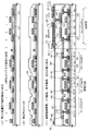
図27は実施例1の記載に基づいて作製されたnチャネル型TFTの特性の一例であり、バイアスー温度(B−T)試験の結果を示す。図27で示すTFTの構造はチャネル長8μm、チャネル幅8μm、Lov=2.5μmでありLoffは設けていない。B−T試験は、ゲート電極に20Vのバイアスを印加して150℃、1時間保持し、その後バイアスを遮断して150℃、1時間の熱処理を加えた。図27はその結果をドレイン電圧(Vd)が1Vと5Vの場合のゲート電圧(VG)対ドレイン電流(ID)の特性で示したものである。ゲート電極とオーバーラップするLDD領域を設けた構造とすることによりホットキャリア効果による劣化が防止され、バイアスストレスによる特性変化は観測されていない。また、下地膜をSiH4、NH3、N2Oから作製される窒酸化シリコン膜(100nm)とSiH4、N2Oから作製される窒酸化シリコン膜(200nm)の2層構造で形成することで、基板に含まれる可動性イオンの影響を除去することが可能となり、B−T試験によるしきい値電圧の変動も観測されていない。
【0158】
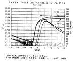
図28(A)、(B)はこのようなTFTを用いて作製したリングオシレータの動特性(電源電圧10V)を示している。リングオシレータは19段である。
図28(A)はLov=2μmとしたときのチャネル長に対する発振周波数の変化を、注入した不純物元素の活性化条件をパラメータとして示している。チャネル長の増加と共に発振周波数は低下するが、活性化条件にはあまり依存していない。ゲート電極とオーバーラップするLDD構造を設けると、その部分による寄生容量の増加により動作周波数の低下が懸念される。しかし、図28(B)で示すように、チャネル長6μmとしてLovの値を1〜3μmまで変化させると、Lovの長さ依存性は観測されるものの、8〜12MHzの周波数で発振させることが可能であり、実用上何ら問題ないことが判明した。
【0159】
このように、下地膜に窒酸化シリコン膜を設け、ゲート電極とオーバーラップするLDD構造を有するTFTは、バイアスや熱によるストレスに対する耐性が高く、またホットキャリア効果による劣化が無く、かつ、高い周波数で動作させることが可能であるので、駆動回路のシフトレジスタ回路やバッファ回路などを形成する上で特に優れている。
【0160】
【発明の効果】
本発明によれば、nチャネル型TFTのチャネル形成領域とドレイン領域との間にLDD領域として、ゲート電極とオーバーラップする第3の不純物領域、ゲート電極とオーバーラップしない第2の不純物領域および第4の不純物領域を設け、異なる動作特性に応じて構造を最適化させたnチャネル型TFTを同一基板上に形成することができる。例えば、アクティブマトリクス基板に形成されるCMOS回路を基本として形成される駆動回路には、ゲート電極とオーバーラップする第3の不純物領域を設けたnチャネル型TFTを形成し、画素部のnチャネル型TFTにはゲート電極とオーバーラップしない第4の不純物領域を設けた構造とすることができる。
【0161】
また、画素部に設ける保持容量を、遮光膜と遮光膜上に形成される誘電体膜と画素電極で形成し、特に遮光膜にAlを用い、誘電体膜を陽極酸化法で形成し、酸化Al膜を用いることで、画像表示に必要な容量を形成するための面積を少なくすることが可能であり、さらに、画素TFT上に形成される遮光膜を保持容量の一方の電極とすることで、アクティブマトリクス型液晶表示装置の画像表示部の開口率を向上させることができた。
【図面の簡単な説明】
【図1】 画素部と周辺駆動回路の作製工程を示す断面図。
【図2】 画素部と周辺駆動回路の作製工程を示す断面図。
【図3】 画素部と周辺駆動回路の作製工程を示す断面図。
【図4】 保持容量の構成を示す断面図。
【図5】 保持容量の作製工程を示す断面図。
【図6】 画素部と周辺駆動回路の作製工程を示す断面図。
【図7】 画素部と周辺駆動回路の作製工程を示す断面図。
【図8】 画素部と周辺駆動回路の作製工程を示す断面図。
【図9】 アクティブマトリクス型液晶表示装置の断面構造図。
【図10】 アクティブマトリクス型液晶表示装置の斜視図。
【図11】 画素部の上面図。
【図12】 保持容量の構成を示す断面図。
【図13】 アクティブマトリクス型液晶表示装置の回路ブロック図。
【図14】 本発明のTFTの構成を示す断面図。
【図15】 結晶質半導体層の作製工程を示す断面図。
【図16】 結晶質半導体層の作製工程を示す断面図。
【図17】 結晶質半導体層の作製工程を示す断面図。
【図18】 半導体装置の一例を示す図。
【図19】 半導体装置の一例を示す図。
【図20】 プロジェクタの一例を示す図。
【図21】 アクティブマトリクス型EL表示装置の上面図及び断面図。
【図22】 アクティブマトリクス型EL表示装置の上面図及び断面図。
【図23】 アクティブマトリクス型EL表示装置の画素部の断面図。
【図24】 アクティブマトリクス型EL表示装置の画素部の上面図及び回路図。
【図25】 アクティブマトリクス型EL表示装置の画素部の断面図。
【図26】 アクティブマトリクス型EL表示装置の画素部の回路図。
【図27】 Lovを設けたTFTのバイアスー温度試験の結果を示すグラフ。
【図28】 Lovを設けたTFTによるリングオシレータの特性を示すグラフ。
【符号の説明】
101 基板
102、103 下地膜
104〜106 半導体層
107 ゲート絶縁膜
120、131、132 ゲート電極
122、123 配線電極
148 第1の層間絶縁膜
149、150、151 ソース配線
152、153 ドレイン配線
154 パッシベーション膜
155 第2の層間絶縁膜
156 遮光膜
157 誘電体膜
160 画素電極
162、163 第5の不純物領域
166、165、171〜173 第1の不純物領域
167、168 第3の不純物領域
174〜177 第4の不純物領域[0001]
BACKGROUND OF THE INVENTION
The present invention relates to a semiconductor device having a circuit including a thin film transistor over a substrate having an insulating surface, and a manufacturing method thereof. In particular, the present invention can be suitably used for an electro-optical device typified by a liquid crystal display device in which a pixel portion and a drive circuit provided in the periphery thereof are provided on the same substrate, and an electronic apparatus equipped with the electro-optical device. Note that in this specification, a semiconductor device refers to all devices that function by utilizing semiconductor characteristics, and includes the above-described electro-optical device and electronic equipment including the electro-optical device in its category.
[0002]
[Prior art]
Development of a semiconductor device having a large-area integrated circuit formed using a thin film transistor (hereinafter referred to as TFT) over a substrate having an insulating surface is in progress. Active matrix liquid crystal display devices, EL display devices, and contact image sensors are known as representative examples. TFTs are classified according to their structure and manufacturing method. In particular, TFTs (referred to as crystalline TFTs) in which a semiconductor film having a crystal structure is an active layer have high field effect mobility, and thus various functional circuits can be formed.
[0003]
For example, in an active matrix liquid crystal display device, a pixel portion or a pixel matrix circuit composed of n-channel TFTs for each functional block, a shift register circuit based on a CMOS circuit, a level shifter circuit, a buffer circuit, and a sampling circuit Etc. were formed on a single substrate. In the contact image sensor, integrated circuits such as a sample hold circuit, a shift register circuit, and a multiplexer circuit are formed using TFTs.
[0004]
The characteristics of a field effect transistor such as a TFT are ideal for a linear region where the drain current and drain voltage increase proportionally, a saturation region where the drain current saturates even when the drain voltage increases, and a drain voltage applied Can be divided into a cut-off region where no current flows. In this specification, the linear region and the saturation region are referred to as the TFT on region, and the blocking region is referred to as the off region. For convenience, the drain current in the on region is referred to as on-current, and the current in the off region is referred to as off-current.
[0005]
Since these circuits do not necessarily have the same operating conditions, the characteristics required for the TFTs are of course different. The pixel portion has a configuration in which a switch element made of an n-channel TFT and an auxiliary storage capacitor are provided, and is driven by applying a voltage to the liquid crystal. Here, the liquid crystal needs to be driven by alternating current, and a method called frame inversion driving has been adopted. Therefore, the required TFT characteristics require that the leakage current be sufficiently reduced. In addition, since a high driving voltage is applied to the buffer circuit, it is necessary to increase the breakdown voltage. In addition, in order to increase the current driving capability, it is necessary to secure a sufficient on-current.
[0006]
However, there is a problem that the off-current of the crystalline TFT tends to be high.
Crystalline TFTs are still considered to be less reliable than MOS transistors (transistors fabricated on a single crystal semiconductor substrate) used in LSI and the like. For example, a deterioration phenomenon such as a decrease in on-current may be observed in a crystalline TFT. This is due to the hot carrier effect, and it has been considered that hot carriers generated by a high electric field near the drain cause a deterioration phenomenon.
[0007]
As a TFT structure, a lightly doped drain (LDD) structure is known. In this structure, a low concentration impurity region is provided between a channel region and a source region or a drain region to which an impurity is added at a high concentration. This low concentration impurity region is called an LDD region. The LDD structure further includes an LDD structure that overlaps with the gate electrode (hereinafter referred to as GOLD (Gate-drain Overlapped LDD)) and an LDD structure that does not overlap with the gate electrode depending on the positional relationship with the gate electrode. . The GOLD structure could relax the high electric field near the drain to prevent the hot carrier effect and improve the reliability. For example, “Mutsuko Hatano, Hajime Akimoto and Takeshi Sakai, IEDM97 TECHNICAL DIGEST, p523-526, 1997” has a GOLD structure with sidewalls made of silicon, but extremely superior reliability compared to TFTs with other structures. Has been confirmed to be obtained.
[0008]
Further, in the pixel portion of the active matrix liquid crystal display device, TFTs are arranged in tens to millions of pixels, and each of the TFTs is provided with a pixel electrode. A counter electrode is provided on the counter substrate side across the liquid crystal, and a kind of capacitor using the liquid crystal as a dielectric has been formed. Then, the potential applied to each pixel is controlled by the switching function of the TFT, and the liquid crystal is driven by controlling the charge to this capacitor to control the amount of transmitted light, thereby displaying an image.
[0009]
Since the capacity of this capacitor gradually decreases due to a leak current, the amount of transmitted light is changed, which causes a decrease in image display contrast. Therefore, conventionally, a capacitor wiring is provided, and a capacitor (holding capacitor) different from a capacitor using liquid crystal as a dielectric is provided in parallel. This holding capacity worked to compensate for the capacity lost by the capacitor using liquid crystal as a dielectric.
[0010]
[Problems to be solved by the invention]
However, the required characteristics are not necessarily the same between the TFT as the switching element of the pixel portion and the TFT of the drive circuit such as a shift register or a buffer circuit. For example, in the TFT of the pixel portion, a large reverse bias voltage (minus if n-channel TFT) is applied to the gate electrode, but a reverse bias voltage is basically applied to the TFT constituting the logic circuit of the drive circuit. Will not work. Further, the operation speed of the former was good at 1/100 or less of the latter. As described above, it is not preferable to use TFTs having the same structure with greatly different operating conditions and required characteristics.
[0011]
In addition, the GOLD structure has a problem that off current becomes larger than that of a normal LDD structure. In order to prevent an increase in off-state current, a multi-gate structure in which a plurality of gates are provided between a pair of source and drain can be used. However, a GOLD structure TFT alone is insufficient. Therefore, it is not always preferable to form all TFTs of a large area integrated circuit with the same structure. For example, in an n-channel TFT in a pixel portion, power consumption increases or abnormality appears in image display when off-current increases, so it is not preferable to apply a GOLD structure crystalline TFT as it is. In addition, the LDD structure that does not overlap with the gate electrode has a problem in that the on-current decreases due to an increase in series resistance. Although the on-current can be freely designed according to the channel width of the TFT, for example, it is not always necessary to provide an LDD structure that does not overlap with the gate electrode in the TFT constituting the buffer circuit.
[0012]
Furthermore, when a storage capacitor using a capacitor wiring is formed in the pixel portion to secure a sufficient capacitance, the aperture ratio has to be sacrificed. In particular, in a small high-definition panel used in a projector type display device, since the pixel area per one is small, a decrease in the aperture ratio due to capacitive wiring has been a problem.
[0013]
The present invention is a technique for solving such a problem, and an object thereof is to realize a crystalline TFT capable of obtaining reliability equal to or higher than that of a MOS transistor. An object of the present invention is to improve the reliability of a semiconductor device having a large-area integrated circuit in which various functional circuits are formed using such crystalline TFTs. Another object of the present invention is to improve the aperture ratio of an active matrix liquid crystal display device with respect to the structure of a TFT and a storage capacitor in a pixel portion.
[0014]
[Means for Solving the Problems]
In order to solve the above problems, according to the structure of the present invention, in a semiconductor device in which a driver circuit and a pixel portion are formed using thin film transistors over the same substrate, the driver circuit forms a channel formation region and a GOLD structure. A first thin film transistor having a first conductivity type third impurity region and a one conductivity type first impurity region forming a source region or a drain region provided outside the gate electrode; a channel formation region; The third impurity region of one conductivity type forming the GOLD structure, the second impurity region of one conductivity type forming the LDD structure provided outside the gate electrode, and the one forming the source region or the drain region A second thin film transistor having a first impurity region of conductivity type, a channel formation region, and a conductor for forming an LDD structure provided outside the gate electrode A third thin film transistor having a second impurity region of a type and a first impurity region of one conductivity type forming a source region or a drain region; a one conductivity type forming a channel formation region and a source region or a drain region; Is provided with a fifth thin film transistor having a fifth impurity region of the opposite conductivity type in consideration of operating characteristics required for the thin film transistor for each functional circuit, and the pixel portion includes a channel formation region, Provided is a fourth thin film transistor having a first conductivity type fourth impurity region forming an LDD structure provided outside the gate electrode and a first conductivity type first impurity region forming a source region or a drain region. It is characterized by having a configuration.
[0015]
In another aspect of the invention, a storage capacitor provided in the pixel portion includes a light-shielding film formed over the fourth thin film transistor through an insulating layer, a pixel electrode connected to the fourth thin film transistor, The light-shielding film, a dielectric film in contact with the light-shielding film, and a pixel electrode in contact with the dielectric film, wherein the storage capacitor is connected to the fourth thin film transistor. Yes. The light-shielding film is preferably made of a material mainly containing one or more elements selected from aluminum, tantalum, and titanium, and the dielectric film is preferably an oxide of the light-shielding film material. Alternatively, the dielectric film may be formed of a material selected from silicon nitride, silicon oxide, silicon nitride oxide, DLC, and polyimide.
[0016]
In order to solve the above problems, a method for manufacturing a semiconductor device of the present invention includes a step of forming a plurality of island-shaped semiconductor layers over a substrate having an insulating surface, and a gate insulating film in contact with the island-shaped semiconductor layers. Forming a gate electrode in contact with the gate insulating film, adding one conductivity type impurity element to a selected region of the island-shaped semiconductor layer, and a first impurity region; Forming a first thin film transistor having a third impurity region overlapping with the gate electrode; adding an impurity element of one conductivity type to a selected region of the island-shaped semiconductor layer; Forming a second thin film transistor having an impurity region, a third impurity region overlapping with the gate electrode, and a second impurity region not overlapping with the gate electrode; Adding a pure element to a selected region of the island-shaped semiconductor layer to form a third thin film transistor having a first impurity region and a second impurity region which does not overlap the gate electrode; Adding an impurity element having a conductivity type opposite to the one conductivity type to a selected region of the island-shaped semiconductor layer to form a fifth thin film transistor having a fifth impurity region; Adding an impurity element to a selected region of the island-shaped semiconductor layer to form a fourth thin film transistor having a first impurity region and a fourth impurity region that does not overlap with the gate electrode; It is characterized by having. The first to fifth thin film transistors are formed on the same substrate in the same process in consideration of operation characteristics required for the thin film transistors for each functional circuit.
[0017]
According to another aspect of the invention, a storage capacitor provided in the pixel portion includes a step of forming an insulating layer on the fourth thin film transistor, a step of forming a light shielding film on the insulating film, and the light shielding film. Preferably, the step of forming a dielectric film in contact with the light-shielding film is formed by a step of forming a dielectric film in contact with the dielectric film and a step of forming a conductive film in contact with the dielectric film. It is a form. Therefore, it is desirable that the light shielding film is formed of a material mainly composed of one or more elements selected from aluminum, tantalum, and titanium.
[0018]
DETAILED DESCRIPTION OF THE INVENTION
[Embodiment 1]
An embodiment of the present invention will be described with reference to FIGS. Here, a method for simultaneously manufacturing a pixel portion and a TFT of a driver circuit provided around the pixel portion will be described.
[0019]
(Process for forming island-like semiconductor layer and gate insulating film)
In FIG. 1, it is desirable to use a non-alkali glass substrate or a quartz substrate for the
[0020]
(Formation of first low-concentration impurity region)
In order to form a low-concentration impurity region serving as an LDD region in the n-channel TFT of the driver circuit, the entire surface of the island-shaped semiconductor layers 104 and 106 and the channel formation region of the island-shaped
This first low-concentration impurity region is for forming an LDD region in an n-channel TFT, and overlaps with the gate electrode and a second impurity region that does not overlap with the gate electrode later due to the positional relationship with the gate electrode. It is distinguished from the third impurity region.
[0021]
Thereafter, a heat treatment was performed in a nitrogen atmosphere at 400 to 900 ° C., preferably 550 to 800 ° C. for 1 to 12 hours, and a step of activating the impurity element imparting n-type added in this step was performed (see FIG. 1 (B)).
[0022]
(Formation of conductive film for gate electrode and wiring)
The first
[0023]
In the case where a Ta film is used for the second
Therefore, the first
[0024]
In addition, when the second conductive film is formed of a W film, argon (Ar) gas and nitrogen (N 2 ) A gas is introduced to form the first
[0025]
(Formation of gate electrode (p-ch), wiring electrode and formation of fifth impurity region)
Resist
[0026]
(Formation of gate electrode (n-ch))
Resist
[0027]
(Formation of first impurity region)
Resist
[0028]
(Formation of second low-concentration impurity region)
In order to form a low-concentration impurity region (referred to as a fourth impurity region in the present invention) in the island-shaped
[0029]
(Thermal activation process)
A first
[0030]
(Formation of source / drain wiring and interlayer insulation film)
Thereafter, contact holes reaching the source region and the drain region of the respective TFTs were formed in the first
Advantages of using the organic resin film are that the film forming method is simple, the relative dielectric constant is low, the parasitic capacitance can be reduced, and the flatness is excellent. Organic resin films other than those described above can also be used. Here, it was formed by baking at 300 ° C. using a type of polyimide that is thermally polymerized after being applied to the substrate.
[0031]
(Formation of storage capacitor and pixel electrode)
A
[0032]
Specifically, as a result of forming an Al oxide film on the Al film by an anodic oxidation method, forming a 0.785
[0033]
Then, a contact hole reaching the
[0034]
Through the above steps, an n-
[0035]
In the p-channel TFT 181 of the driver circuit, a
[0036]
The n-
[0037]
In the present invention, in consideration of the operating environment of the n-channel TFT of each of the pixel portion and the driver circuit, the second impurity region, the third impurity region, and the fourth impurity region, which become the LDD regions, in the channel length direction The lengths were made different on the same substrate, and an optimum shape could be created for the TFTs constituting each circuit. The n-
[0038]
As described above, the present invention can improve the operation performance and reliability of a semiconductor device by optimizing the structure of TFTs constituting each circuit in accordance with specifications required by the pixel portion and the drive circuit. It can be. Specifically, the design of the LDD region of the n-channel TFT is varied depending on each circuit specification, and an LDD region that overlaps or does not overlap with the gate electrode is appropriately provided, thereby providing the same substrate. In addition, it is possible to realize a TFT structure that places importance on measures against hot carrier deterioration and a TFT structure that places importance on low off-current values.
[0039]
[Embodiment 2]
Another structure of the storage capacitor connected to the n-channel TFT in the pixel portion of the active matrix substrate will be described. FIG. 4 is a cross-sectional structure diagram of a pixel portion of an active matrix substrate manufactured in the same manner as in the first embodiment.
[0040]
[0041]
The
[0042]
[Embodiment 3]
FIG. 5 shows another structure of the storage capacitor connected to the n-channel TFT in the pixel portion. FIG. 5A illustrates an n-channel TFT of a pixel portion manufactured in the same manner as in
[0043]
【Example】
[Example 1]
In this embodiment, an example of manufacturing a pixel portion and a driver circuit thereof over the same substrate using the present invention will be described with reference to FIGS. In this specification, such a substrate is referred to as an active matrix substrate for convenience. First, a silicon
The silicon
Thereafter, a heat treatment at 450 to 650 ° C. was performed in a nitrogen atmosphere to densify the
[0044]
Next, resist
[0045]
The first
[0046]
Next, resist
Etching of TaN film and Ta film is CF Four And O 2 It was possible to carry out with a mixed gas of Then, a process of adding an impurity element imparting p-type to a part of the island-shaped
[0047]
A
[0048]
After removing the resist mask provided in FIG. 7A, resist
[0049]
As described above, the
[0050]
Then, new resist
[0051]
In order to form the second low-concentration impurity region which becomes the LDD region of the n-channel TFT in the pixel portion in the island-shaped
[0052]
Then, the first
[0053]
Thereafter, a predetermined resist mask was formed on the first insulating
[0054]
Then, a
[0055]
Thereafter, a second
[0056]
When the insulating
The
[0057]
The p-
On the other hand, the n-
The n-channel TFT 703 includes a
The n-
[0058]
As described above, the present invention can improve the operation performance and reliability of a semiconductor device by optimizing the structure of TFTs constituting each circuit in accordance with specifications required by the pixel portion and the drive circuit. It can be. For example, the n-
[0059]
[Example 2]
In this example, a process of manufacturing an active matrix liquid crystal display device from an active matrix substrate will be described. As shown in FIG. 9, an alignment film 901 is formed on the substrate in the state of FIG. Usually, a polyimide resin is often used for the alignment film of the liquid crystal display element. A transparent conductive film 903 and an alignment film 904 were formed on the
[0060]
Next, the configuration of the active matrix liquid crystal display device will be described with reference to the perspective view of FIG. 10 and the top view of FIG. Note that FIGS. 10 and 11 use the same reference numerals in order to correspond to the cross-sectional structure diagrams of FIGS. The active matrix substrate includes a
[0061]
FIG. 11 is a top view illustrating a part of the
Further, the cross-sectional structure along AA ′ shown in FIG. 11 corresponds to the AA ′ cross-sectional view of the pixel portion shown in FIG.
[0062]
[Example 3]
FIG. 12 shows another configuration example of a method for connecting a storage capacitor provided in the TFT of the pixel portion. FIG. 12 is a cross-sectional structure diagram of a pixel portion of an active matrix substrate manufactured in the same manner as in the first embodiment.
[0063]
In FIG. 12A, a
[0064]
[Example 4]
FIG. 13 shows an example of a circuit configuration of the active matrix substrate shown in the first embodiment. The active matrix substrate of this embodiment includes a source signal line side driver circuit 1301, a gate signal line side driver circuit (A) 1307, a gate signal line side driver circuit (B) 1311, a precharge circuit 1312, and a pixel portion 1306. ing. The source signal line side driver circuit 1301 includes a shift register circuit 1302, a level shifter circuit 1303, a buffer circuit 1304, and a sampling circuit 1305. The gate signal line side driver circuit (A) 1307 includes a
[0065]
Here, as an example of the driving voltage of each circuit, the
[0066]
FIG. 14A illustrates a configuration example of a TFT of the shift register circuit. The n-channel TFT of the shift register circuit has a single gate structure, and third impurity regions (LDD regions) 205 and 206 that overlap the
[0067]
FIG. 14B shows a configuration example of TFTs of a level shifter circuit and a buffer circuit. The n-channel TFTs of these circuits have a double gate structure, but of course there is no problem with a single gate structure. This n-channel TFT also has a structure in which third impurity regions (LDD regions) 205a, 205b, 206a, and 206b overlapping with the
[0068]
FIG. 14C shows a configuration example of a TFT of the sampling circuit. The n-channel TFT of this circuit has a single gate structure, but the LDD region that overlaps the gate electrode on both the source side and the drain side corresponds to driving with polarity inversion outside the channel formation region.
[0069]
FIG. 14D illustrates a structure suitable for a driver circuit that operates at a high speed with a driving voltage of about 1.5 to 5 V. The n-channel TFT in the
[0070]
[Example 5]
In this embodiment, a method for manufacturing a semiconductor layer which can be applied to the present invention will be described. In FIG. 15, the substrate 1501 can be a glass substrate, a ceramic substrate, a quartz substrate, or the like. Alternatively, a silicon substrate on which an insulating film such as a silicon oxide film or a silicon nitride film is formed or a metal substrate typified by stainless steel may be used. In the case of using a glass substrate, it is desirable to perform heat treatment in advance at a temperature below the strain point. For example, in the case of using a # 1737 substrate manufactured by Corning, heat treatment may be performed at 500 to 650 ° C., preferably 595 to 645 ° C. for 1 to 24 hours.
[0071]
Then, a base film was formed on the main surface of the substrate 1501. There is no particular limitation on the material of the base film, but the silicon nitride oxide film 1502 is used. In addition, a single layer or a plurality of layers selected from a silicon nitride film, a silicon oxide film, a silicon nitride oxide film, and a tantalum oxide film can be used. In the case of using a silicon nitride oxide film, it may be formed to a thickness of 20 to 100 nm, typically 50 nm. Further, a silicon nitride oxide film may be formed to a thickness of 50 to 500 nm, typically 50 to 200 nm, on a 10 to 100 nm silicon nitride film. An amorphous semiconductor layer 1503 was formed thereon. This may be an amorphous semiconductor formed by a film formation method such as a plasma CVD method, a low pressure CVD method, or a sputtering method, and includes silicon (Si), germanium (Ge), silicon germanium alloy, and silicon carbide. In addition, a compound semiconductor material such as gallium arsenide can be used. The semiconductor layer was formed to a thickness of 10 to 100 nm, typically 50 nm. In addition, the base film 1501 and the amorphous semiconductor layer 1503 can be continuously formed by a plasma CVD method or a sputtering method. After each layer is formed, the surface can be prevented from being contaminated by preventing the surface from being exposed to the air atmosphere (FIG. 15A).
[0072]
Next, a crystallization step was performed. A known laser crystallization technique or thermal crystallization technique may be used for the step of crystallizing the amorphous semiconductor layer. In addition, the amorphous semiconductor layer manufactured by the plasma CVD method contains hydrogen in the film at a rate of 10 to 40 atomic%, and a heat treatment process at 400 to 500 ° C. is performed prior to the crystallization process. It was desirable to desorb hydrogen from the film so that the amount of hydrogen contained was 5 atomic% or less (FIG. 15B). Then, an island-shaped crystalline semiconductor layer 1505 was formed from the crystalline semiconductor layer 1504, and a gate insulating film 1505 was further formed. The gate insulating film 1505 may be formed using a material such as a silicon nitride film, a silicon oxide film, or a silicon nitride oxide film. The gate insulating film 1505 may be formed to a thickness of 10 to 1000 nm, preferably 50 to 400 nm. Subsequent steps can be performed according to
[0073]
In FIG. 16, a base film 1602 made of a silicon oxynitride film is formed on the main surface of the substrate 1601, and an amorphous semiconductor layer 1603 is formed on the surface as in FIG. The thickness of the amorphous semiconductor layer may be 10 to 200 nm, preferably 30 to 100 nm. Further, an aqueous solution containing 10 ppm of the catalytic element in terms of weight was applied by a spin coating method, so that the catalytic element-containing layer 1604 was formed on the entire surface of the amorphous semiconductor layer 1603. In addition to nickel (Ni), usable catalyst elements include germanium (Ge), iron (Fe), palladium (Pd), tin (Sn), lead (Pb), cobalt (Co), platinum ( Pt), copper (Cu), gold (Au), and the like. The internal stress of the amorphous semiconductor layer was not uniformly determined by the manufacturing conditions. However, it was necessary to desorb hydrogen from the film by performing a heat treatment step at 400 to 600 ° C. prior to the crystallization step (FIG. 16A). Then, heat treatment was performed at 500 to 600 ° C. for 4 to 12 hours, for example, 550 ° C. for 8 hours, and a crystalline semiconductor layer 1605 was formed (FIG. 16B).
[0074]
Next, a gettering step for removing the catalyst element used in the crystallization step from the crystalline semiconductor film was performed. By this gettering step, the concentration of the catalytic element in the crystalline semiconductor film is reduced to 1 × 10. 17 atms / cm Three Or less, preferably 1 × 10 16 atms / cm Three It was possible to reduce to. First, a mask insulating film 1606 was formed to a thickness of 150 nm on the surface of the crystalline semiconductor layer 1605, an
In this state, when heat treatment is performed in a nitrogen atmosphere at 550 to 800 ° C. for 5 to 24 hours, for example, 600 ° C. for 12 hours, the phosphorus-containing
[0075]
In FIG. 17, a base film 1702 and an amorphous semiconductor layer 1703 are formed in this order over a substrate 1701, and a mask insulating film 1704 is formed on the surface of the amorphous semiconductor layer 1703. At this time, the thickness of the mask insulating film 1704 was set to 150 nm. Further, the mask insulating film 1704 was patterned to selectively form
The crystalline semiconductor layer 1707 formed in this way is composed of a collection of rod-like or needle-like crystals, and each crystal grows with a specific direction as viewed macroscopically, so that the crystallinity is uniform. (FIG. 17B).
[0076]
Next, similarly to FIG. 16, a step of removing the catalyst element used in the crystallization step from the crystalline semiconductor film was performed. A step of adding phosphorus was performed on the substrate in the same state as FIG. 17B, so that a phosphorus-containing
[0077]
Then, the mask insulating film 1704 and the phosphorus-containing
[0078]
[Example 6]
In this embodiment, a semiconductor device incorporating an active matrix liquid crystal display device using a TFT circuit of the present invention will be described with reference to FIGS.
[0079]
Examples of such a semiconductor device include a portable information terminal (electronic notebook, mobile computer, mobile phone, etc.), a video camera, a still camera, a personal computer, a television, and the like. An example of these is shown in FIG.
[0080]
FIG. 18A illustrates a mobile phone, which includes a main body 9001, an
[0081]
FIG. 18B illustrates a video camera which includes a main body 9101, a display device 9102, an
[0082]
FIG. 18C illustrates a mobile computer, which includes a main body 9201, a camera portion 9202, an image receiving portion 9203, operation switches 9204, and a display device 9205. The present invention can be applied to the image receiving portion 9203 and a display device 9205 including an active matrix substrate.
[0083]
FIG. 18D illustrates a head mounted display which includes a main body 9301, a
[0084]
FIG. 18E illustrates a rear projector, which includes a main body 9401, a light source 9402, a
[0085]
FIG. 18F illustrates a portable book, which includes a main body 9501,
[0086]
FIG. 19A illustrates a personal computer, which includes a main body 2401, an
[0087]
FIG. 19B shows a player using a recording medium (hereinafter referred to as a recording medium) in which a program is recorded, and includes a main body 2413, a
The present invention can be applied to the
[0088]
FIG. 19C illustrates a digital camera which includes a main body 2418, a
[0089]
FIG. 20A illustrates a front type projector, which includes a
[0090]
FIG. 20B shows a rear projector, which includes a
[0091]
20C is a diagram showing an example of the structure of the
[0092]
FIG. 20D is a diagram illustrating an example of the structure of the light source
[0093]
Although not shown here, the present invention can also be applied to an image sensor and an EL display element. As described above, the scope of application of the present invention is extremely wide and can be applied to electronic devices in various fields.
[0094]
Although not shown here, the present invention can also be applied to a display unit of a car navigation system or an image sensor personal computer. As described above, the scope of application of the present invention is extremely wide and can be applied to electronic devices in various fields.
[0095]
[Example 7]
In this example, an example in which an EL (electroluminescence) display device is manufactured using the present invention will be described.
[0096]
FIG. 21A is a top view of an EL display device using the present invention. In FIG. 21A,
[0097]
At this time, a
[0098]
FIG. 21B shows a cross-sectional structure of the EL display device of this embodiment. A driver circuit TFT (here, an n-channel TFT and a p-channel TFT are combined on a
[0099]
The present invention can be used for the
[0100]
When the driving
[0101]
Next, an
[0102]
In this embodiment, the EL layer is formed by vapor deposition using a shadow mask. Color display is possible by forming a light emitting layer (a red light emitting layer, a green light emitting layer, and a blue light emitting layer) capable of emitting light having different wavelengths for each pixel using a shadow mask. In addition, there are a method in which a color conversion layer (CCM) and a color filter are combined, and a method in which a white light emitting layer and a color filter are combined, but either method may be used.
Needless to say, an EL display device emitting monochromatic light can also be used.
[0103]
After the
[0104]
In this embodiment, a stacked structure of a LiF (lithium fluoride) film and an Al (aluminum) film is used as the
[0105]
In order to electrically connect the
[0106]
A
[0107]
Further, a sealing material is provided inside the
[0108]
At this time, the
[0109]
In addition, a spacer may be included in the
[0110]
In the case where a spacer is provided, the
[0111]
As the
[0112]
However, the
[0113]
The
[0114]
Further, an example in which an EL display device with a different form is manufactured will be described with reference to FIGS. The same reference numerals as those in FIGS. 21A and 21B indicate the same parts, and the description thereof is omitted.
[0115]
FIG. 22A is a top view of the EL display device of this embodiment, and FIG. 22B is a cross-sectional view taken along line AA ′ of FIG.
[0116]
In the same manner as shown in FIG. 21, a
[0117]
Further, a
[0118]
In addition, a spacer may be included in the
[0119]
In the case where a spacer is provided, the
[0120]
As the
[0121]
However, the
[0122]
Next, after the
[0123]
The
[0124]
FIG. 23 shows a detailed cross-sectional structure of the pixel portion of the EL display device, FIG. 24A shows a top structure, and FIG. 24B shows a circuit diagram. 23, 24 (A), and 24 (B) use common reference numerals and may be referred to each other.
[0125]
In FIG. 23, a switching
[0126]
The
[0127]
At this time, it is very important that the
[0128]
In this embodiment, the
[0129]
Further, as shown in FIG. 24A, a wiring to be a
[0130]
A
[0131]
As the
[0132]
In addition, a
[0133]
There are various types of PPV organic EL materials such as “H. Shenk, H. Becker, O. Gelsen, E. Kluge, W. Kreuder, and H. Spreitzer,“ Polymers for Light Emitting ”. Materials such as those described in “Diodes”, Euro Display, Proceedings, 1999, p. 33-37 ”and Japanese Patent Laid-Open No. 10-92576 may be used.
[0134]
As a specific light emitting layer, cyanopolyphenylene vinylene may be used for a light emitting layer that emits red light, polyphenylene vinylene may be used for a light emitting layer that emits green light, and polyphenylene vinylene or polyalkylphenylene may be used for a light emitting layer that emits blue light. The film thickness may be 30 to 150 nm (preferably 40 to 100 nm).
[0135]
However, the above example is an example of an organic EL material that can be used as a light emitting layer, and is not necessarily limited to this. An EL layer (a layer for emitting light and moving carriers therefor) may be formed by freely combining a light-emitting layer, a charge transport layer, or a charge injection layer.
[0136]
For example, in this embodiment, an example in which a polymer material is used as the light emitting layer is shown, but a low molecular weight organic EL material may be used. It is also possible to use an inorganic material such as silicon carbide for the charge transport layer or the charge injection layer. As these organic EL materials and inorganic materials, known materials can be used.
[0137]
In this embodiment, an EL layer having a stacked structure in which a
[0138]
When the
[0139]
Incidentally, in this embodiment, a
[0140]
As described above, the EL display panel of the present invention has a pixel portion composed of pixels having a structure as shown in FIG. 23. Have. Therefore, an EL display panel having high reliability and capable of displaying a good image can be obtained.
[0141]
Note that the configuration in FIG. 23 can be implemented by freely combining with the configurations of the first embodiment and the first to fourth embodiments. Further, it is effective to use the EL display device of this embodiment as the display unit of the electronic apparatus of
[0142]
As another structure of the pixel portion, a structure in which the structure of the
[0143]
In FIG. 25, a current control TFT 3103 is formed using the p-channel TFT of the present invention. For the manufacturing process,
[0144]
In FIG. 25, a transparent conductive film is used as the pixel electrode (anode) 3050. Specifically, a conductive film made of a compound of indium oxide and zinc oxide is used. Of course, a conductive film made of a compound of indium oxide and tin oxide may be used.
[0145]
Then, after
[0146]
The light generated in the
[0147]
The configuration in FIG. 25 can be implemented by freely combining with the configurations in the first embodiment and the first to fourth embodiments. Further, it is effective to use the EL display panel of this embodiment as the display unit of the electronic apparatus of
[0148]
Examples of a pixel having a structure different from the circuit diagram illustrated in FIG. 24B are illustrated in FIGS. In this embodiment, 3201 is a source wiring of the switching
[0149]
FIG. 26A shows an example in which the
[0150]
FIG. 26B illustrates an example in which the
[0151]
In FIG. 26C, similarly to the structure of FIG. 21B, the
[0152]
Note that the circuit configuration shown in FIG. 26 can be freely combined with the configurations of the first embodiment and the first to fourth embodiments. In addition, it is effective to use the EL display device having the pixel structure of this embodiment as the display unit of the electronic apparatus of
[0153]
In FIGS. 24A and 24B, a
[0154]
Since the capacitance of the parasitic capacitance varies depending on the area where the gate electrode and the GOLD region overlap, the capacitance of the parasitic capacitance is determined by the length of the GOLD region included in the overlapping region.
[0155]
Similarly, in the structures of FIGS. 26A, 26B, and 26C, the
[0156]
Such a configuration can be implemented by freely combining with the configurations of the first embodiment and the first to fourth embodiments. In addition, it is effective to use the EL display device having the pixel structure of this embodiment as the display unit of the electronic apparatus of
[0157]
[Example 8]
FIG. 27 shows an example of the characteristics of an n-channel TFT manufactured based on the description in Example 1, and shows the result of a bias temperature (BT) test. The TFT structure shown in FIG. 27 has a channel length of 8 μm, a channel width of 8 μm, Lov = 2.5 μm, and Loff is not provided. In the BT test, a bias of 20 V was applied to the gate electrode and held at 150 ° C. for 1 hour, and then the bias was cut off and a heat treatment was applied at 150 ° C. for 1 hour. FIG. 27 shows the result as a characteristic of gate voltage (VG) versus drain current (ID) when the drain voltage (Vd) is 1V and 5V. The structure provided with the LDD region overlapping with the gate electrode prevents deterioration due to the hot carrier effect, and no characteristic change due to bias stress is observed. Also, the base film is SiH Four , NH Three , N 2 Silicon oxynitride film (100 nm) made from O and SiH Four , N 2 By forming a silicon oxynitride film (200 nm) made of O with a two-layer structure, it becomes possible to remove the influence of mobile ions contained in the substrate, and the threshold voltage fluctuations due to the BT test Has not been observed.
[0158]
28A and 28B show dynamic characteristics (power supply voltage 10 V) of a ring oscillator manufactured using such TFTs. The ring oscillator has 19 stages.
FIG. 28A shows the change of the oscillation frequency with respect to the channel length when Lov = 2 μm, with the activation condition of the implanted impurity element as a parameter. Although the oscillation frequency decreases with increasing channel length, it does not depend much on the activation conditions. When an LDD structure overlapping with the gate electrode is provided, there is a concern that the operating frequency may decrease due to an increase in parasitic capacitance due to the portion. However, as shown in FIG. 28 (B), if the channel length is 6 μm and the value of Lov is changed from 1 to 3 μm, the length dependency of Lov is observed, but oscillation can occur at a frequency of 8 to 12 MHz. It was found that there was no problem in practical use.
[0159]
As described above, a TFT having an LDD structure in which a silicon oxynitride film is provided as a base film and overlapped with a gate electrode has high resistance to stress due to bias and heat, is not deteriorated by a hot carrier effect, and has a high frequency. Therefore, it is particularly excellent in forming a shift register circuit or a buffer circuit of a driver circuit.
[0160]
【The invention's effect】
According to the present invention, as the LDD region between the channel formation region and the drain region of the n-channel TFT, the third impurity region that overlaps the gate electrode, the second impurity region that does not overlap the gate electrode, and the second impurity region Thus, an n-channel TFT having four impurity regions and having an optimized structure according to different operating characteristics can be formed on the same substrate. For example, in a driver circuit formed on the basis of a CMOS circuit formed on an active matrix substrate, an n-channel TFT provided with a third impurity region overlapping with a gate electrode is formed, and an n-channel TFT in a pixel portion is formed. The TFT can have a structure in which a fourth impurity region which does not overlap with the gate electrode is provided.
[0161]
In addition, the storage capacitor provided in the pixel portion is formed by a light shielding film, a dielectric film formed on the light shielding film, and a pixel electrode. In particular, Al is used for the light shielding film, and the dielectric film is formed by an anodic oxidation method. By using the Al film, it is possible to reduce the area for forming the capacitance necessary for image display, and further, by using the light shielding film formed on the pixel TFT as one electrode of the storage capacitor. Thus, the aperture ratio of the image display portion of the active matrix liquid crystal display device can be improved.
[Brief description of the drawings]
FIG. 1 is a cross-sectional view illustrating a manufacturing process of a pixel portion and a peripheral driver circuit.
FIG. 2 is a cross-sectional view illustrating a manufacturing process of a pixel portion and a peripheral driver circuit.
FIG. 3 is a cross-sectional view illustrating a manufacturing process of a pixel portion and a peripheral driver circuit.
FIG. 4 is a cross-sectional view illustrating a configuration of a storage capacitor.
FIG. 5 is a cross-sectional view illustrating a manufacturing process of a storage capacitor.
FIG. 6 is a cross-sectional view illustrating a manufacturing process of a pixel portion and a peripheral driver circuit.
FIG. 7 is a cross-sectional view illustrating a manufacturing process of a pixel portion and a peripheral driver circuit.
FIG. 8 is a cross-sectional view illustrating a manufacturing process of a pixel portion and a peripheral driver circuit.
FIG. 9 is a cross-sectional structure diagram of an active matrix liquid crystal display device.
FIG. 10 is a perspective view of an active matrix liquid crystal display device.
FIG. 11 is a top view of a pixel portion.
FIG. 12 is a cross-sectional view illustrating a configuration of a storage capacitor.
FIG. 13 is a circuit block diagram of an active matrix liquid crystal display device.
FIG. 14 is a cross-sectional view showing a structure of a TFT of the present invention.
FIG. 15 is a cross-sectional view illustrating a manufacturing process of a crystalline semiconductor layer.
FIG. 16 is a cross-sectional view illustrating a manufacturing process of a crystalline semiconductor layer.
FIG. 17 is a cross-sectional view illustrating a manufacturing process of a crystalline semiconductor layer.
FIG 18 illustrates an example of a semiconductor device.
FIG 19 illustrates an example of a semiconductor device.
FIG. 20 shows an example of a projector.
FIGS. 21A and 21B are a top view and a cross-sectional view of an active matrix EL display device. FIGS.
22A and 22B are a top view and a cross-sectional view of an active matrix EL display device.
FIG. 23 is a cross-sectional view of a pixel portion of an active matrix EL display device.
FIGS. 24A and 24B are a top view and a circuit diagram of a pixel portion of an active matrix EL display device. FIGS.
FIG. 25 is a cross-sectional view of a pixel portion of an active matrix EL display device.
FIG. 26 is a circuit diagram of a pixel portion of an active matrix EL display device.
FIG. 27 is a graph showing the result of a bias-temperature test of a TFT provided with Lov.
FIG. 28 is a graph showing the characteristics of a ring oscillator using TFTs provided with Lov.
[Explanation of symbols]
101 substrate
102, 103 Underlayer
104-106 semiconductor layer
107 Gate insulation film
120, 131, 132 Gate electrode
122, 123 Wiring electrode
148 First interlayer insulating film
149, 150, 151 Source wiring
152, 153 Drain wiring
154 Passivation film
155 Second interlayer insulating film
156 light shielding film
157 Dielectric film
160 pixel electrode
162, 163 fifth impurity region
166, 165, 171 to 173 First impurity region
167, 168 Third impurity region
174 to 177 Fourth impurity region
Claims (10)
前記駆動回路は、
ゲート絶縁膜を挟んでゲート電極と全部が重なるように配置されたLDD領域を有する第1の駆動TFTと、
ゲート絶縁膜を挟んでゲート電極と一部が重なるように配置されたLDD領域を有する第2の駆動TFTと、を含み、
前記画素部は、ゲート絶縁膜を挟んでゲート電極と重ならないように配置されたLDD領域を有する画素TFTを含み、
前記画素部の保持容量は、前記画素TFTの上方に設けられた遮光膜、前記遮光膜上に形成された誘電体膜および画素電極で形成されていることを特徴とする半導体装置。A driving circuit and a pixel portion on the same substrate;
The drive circuit is
A first driving TFT having an LDD region disposed so as to entirely overlap the gate electrode with the gate insulating film interposed therebetween;
A second driving TFT having an LDD region disposed so as to partially overlap the gate electrode with the gate insulating film interposed therebetween,
The pixel portion includes a pixel TFT having an LDD region arranged so as not to overlap the gate electrode with a gate insulating film interposed therebetween,
2. The semiconductor device according to claim 1, wherein the storage capacitor of the pixel portion is formed of a light shielding film provided above the pixel TFT, a dielectric film formed on the light shielding film, and a pixel electrode.
前記駆動回路は、
ゲート絶縁膜を挟んでゲート電極と全部が重なるように配置されたLDD領域を有する第1のnチャネル型TFTと、
ゲート絶縁膜を挟んでゲート電極と一部が重なるように配置されたLDD領域を有する第2のnチャネル型TFTと、
pチャネル型TFTと、を含み、
前記画素部は、ゲート絶縁膜を挟んでゲート電極と重ならないように配置されたLDD領域を有する画素TFTを含み、
前記画素部の保持容量は、前記画素TFTの上方に設けられた遮光膜、前記遮光膜上に形成された誘電体膜および画素電極で形成されていることを特徴とする半導体装置。A driving circuit and a pixel portion on the same substrate;
The drive circuit is
A first n-channel TFT having an LDD region disposed so as to entirely overlap the gate electrode with a gate insulating film interposed therebetween;
A second n-channel TFT having an LDD region disposed so as to partially overlap the gate electrode with the gate insulating film interposed therebetween;
a p-channel TFT,
The pixel portion includes a pixel TFT having an LDD region arranged so as not to overlap the gate electrode with a gate insulating film interposed therebetween,
2. The semiconductor device according to claim 1, wherein the storage capacitor of the pixel portion is formed of a light shielding film provided above the pixel TFT, a dielectric film formed on the light shielding film, and a pixel electrode.
前記遮光膜は、アルミニウム、タンタル、チタンから選ばれた一種または複数種を主成分とする材料から成ることを特徴とする半導体装置。In claim 1 or claim 2 ,
The light-shielding film is made of a material mainly composed of one or more selected from aluminum, tantalum, and titanium.
前記誘電体膜は、前記遮光膜の酸化物であることを特徴とする半導体装置。In any one of claims 1 to 3,
The semiconductor device, wherein the dielectric film is an oxide of the light shielding film.
前記誘電体膜は、窒化シリコン、酸化シリコン、窒酸化シリコン、DLC、ポリイミドから選ばれた材料で形成されていることを特徴とする半導体装置。In any one of claims 1 to 3,
The semiconductor device, wherein the dielectric film is formed of a material selected from silicon nitride, silicon oxide, silicon nitride oxide, DLC, and polyimide.
前記駆動回路を形成する第1のnチャネル型TFTの島状半導体層に、チャネル形成領域、ソース領域、ドレイン領域、及び、ゲート絶縁膜を挟んでゲート電極と全部が重なるように配置されたLDD領域を形成し、
前記駆動回路を形成する第2のnチャネル型TFTの島状半導体層に、チャネル形成領域、ソース領域、ドレイン領域、及び、ゲート絶縁膜を挟んでゲート電極と一部が重なるように配置されたLDD領域を形成し、
前記駆動回路を形成するpチャネル型TFTの島状半導体層に、チャネル形成領域、ソース領域、及びドレイン領域を形成し、
前記画素部を形成する画素TFTの島状半導体層に、チャネル形成領域、ソース領域、ドレイン領域、及び、ゲート絶縁膜を挟んでゲート電極と重ならないように配置されたLDD領域を形成し、
前記画素TFTの上方に設けられた遮光膜、前記遮光膜上に形成された誘電体膜および画素電極で前記画素部の保持容量を形成することを特徴とする半導体装置の作製方法。In a method for manufacturing a semiconductor device including a driver circuit and a pixel portion over the same substrate,
An LDD disposed on the island-like semiconductor layer of the first n-channel TFT forming the driving circuit so that the gate electrode overlaps with the channel formation region, the source region, the drain region, and the gate insulating film. Forming a region,
The second n-channel TFT forming the driving circuit is disposed on the island-shaped semiconductor layer so as to partially overlap the gate electrode with the channel formation region, the source region, the drain region, and the gate insulating film interposed therebetween. Forming an LDD region;
Forming a channel formation region, a source region, and a drain region in an island-shaped semiconductor layer of a p-channel TFT forming the driving circuit;
An LDD region is formed in the island-shaped semiconductor layer of the pixel TFT forming the pixel portion so as not to overlap the gate electrode with the channel formation region, the source region, the drain region, and the gate insulating film interposed therebetween,
A manufacturing method of a semiconductor device, wherein a storage capacitor of the pixel portion is formed by a light shielding film provided above the pixel TFT, a dielectric film formed on the light shielding film, and a pixel electrode.
前記遮光膜は、アルミニウム、タンタル、チタンから選ばれた一種または複数種を主成分とする材料から成ることを特徴とする半導体装置の作製方法。In claim 7 ,
The method for manufacturing a semiconductor device, wherein the light shielding film is made of a material mainly containing one or more selected from aluminum, tantalum, and titanium.
前記誘電体膜は、前記遮光膜の酸化物であることを特徴とする半導体装置の作製方法。In claim 7 or claim 8 ,
The method for manufacturing a semiconductor device, wherein the dielectric film is an oxide of the light shielding film.
前記誘電体膜は、窒化シリコン、酸化シリコン、窒酸化シリコン、DLC、ポリイミドから選ばれた材料で形成されていることを特徴とする半導体装置の作製方法。In claim 7 or claim 8 ,
The method for manufacturing a semiconductor device, wherein the dielectric film is formed of a material selected from silicon nitride, silicon oxide, silicon nitride oxide, DLC, and polyimide.
Priority Applications (1)
| Application Number | Priority Date | Filing Date | Title |
|---|---|---|---|
| JP2000033377A JP4549475B2 (en) | 1999-02-12 | 2000-02-10 | Semiconductor device, electronic device, and method for manufacturing semiconductor device |
Applications Claiming Priority (3)
| Application Number | Priority Date | Filing Date | Title |
|---|---|---|---|
| JP11-33623 | 1999-02-12 | ||
| JP3362399 | 1999-02-12 | ||
| JP2000033377A JP4549475B2 (en) | 1999-02-12 | 2000-02-10 | Semiconductor device, electronic device, and method for manufacturing semiconductor device |
Related Child Applications (1)
| Application Number | Title | Priority Date | Filing Date |
|---|---|---|---|
| JP2010119143A Division JP5132714B2 (en) | 1999-02-12 | 2010-05-25 | Transmission type liquid crystal display device, projector and digital camera |
Publications (3)
| Publication Number | Publication Date |
|---|---|
| JP2000299469A JP2000299469A (en) | 2000-10-24 |
| JP2000299469A5 JP2000299469A5 (en) | 2007-04-05 |
| JP4549475B2 true JP4549475B2 (en) | 2010-09-22 |
Family
ID=26372351
Family Applications (1)
| Application Number | Title | Priority Date | Filing Date |
|---|---|---|---|
| JP2000033377A Expired - Fee Related JP4549475B2 (en) | 1999-02-12 | 2000-02-10 | Semiconductor device, electronic device, and method for manufacturing semiconductor device |
Country Status (1)
| Country | Link |
|---|---|
| JP (1) | JP4549475B2 (en) |
Families Citing this family (27)
| Publication number | Priority date | Publication date | Assignee | Title |
|---|---|---|---|---|
| US6583471B1 (en) | 1999-06-02 | 2003-06-24 | Semiconductor Energy Laboratory Co., Ltd. | Semiconductor device having first and second insulating films |
| US6580094B1 (en) | 1999-10-29 | 2003-06-17 | Semiconductor Energy Laboratory Co., Ltd. | Electro luminescence display device |
| JP2001195016A (en) * | 1999-10-29 | 2001-07-19 | Semiconductor Energy Lab Co Ltd | Electronic device |
| JP3643025B2 (en) * | 2000-10-20 | 2005-04-27 | シャープ株式会社 | Active matrix display device and manufacturing method thereof |
| US6664732B2 (en) | 2000-10-26 | 2003-12-16 | Semiconductor Energy Laboratory Co., Ltd. | Light emitting device and manufacturing method thereof |
| JP2005100992A (en) * | 2000-10-26 | 2005-04-14 | Semiconductor Energy Lab Co Ltd | Light-emitting device |
| JP4954366B2 (en) * | 2000-11-28 | 2012-06-13 | 株式会社半導体エネルギー研究所 | Method for manufacturing semiconductor device |
| US6825496B2 (en) | 2001-01-17 | 2004-11-30 | Semiconductor Energy Laboratory Co., Ltd. | Light emitting device |
| JP4137454B2 (en) * | 2001-01-17 | 2008-08-20 | 株式会社半導体エネルギー研究所 | Light emitting device, electronic device, and method for manufacturing light emitting device |
| SG138468A1 (en) * | 2001-02-28 | 2008-01-28 | Semiconductor Energy Lab | A method of manufacturing a semiconductor device |
| TW554398B (en) * | 2001-08-10 | 2003-09-21 | Semiconductor Energy Lab | Method of peeling off and method of manufacturing semiconductor device |
| JP4302347B2 (en) * | 2001-12-18 | 2009-07-22 | シャープ株式会社 | Thin film transistor substrate and manufacturing method thereof |
| US6835954B2 (en) | 2001-12-29 | 2004-12-28 | Lg.Philips Lcd Co., Ltd. | Active matrix organic electroluminescent display device |
| TWI255432B (en) * | 2002-06-03 | 2006-05-21 | Lg Philips Lcd Co Ltd | Active matrix organic electroluminescent display device and fabricating method thereof |
| TWI220072B (en) | 2003-02-19 | 2004-08-01 | Toppoly Optoelectronics Corp | TFT structure with LDD region and manufacturing process of the same |
| US7554260B2 (en) * | 2004-07-09 | 2009-06-30 | Semiconductor Energy Laboratory Co., Ltd. | Display device provided with a conductive film connection between a wiring component and a metal electrode film |
| JP4675680B2 (en) | 2005-05-30 | 2011-04-27 | シャープ株式会社 | Method for manufacturing thin film transistor substrate |
| US8803781B2 (en) * | 2007-05-18 | 2014-08-12 | Semiconductor Energy Laboratory Co., Ltd. | Semiconductor device and display device |
| US20100327353A1 (en) * | 2008-01-29 | 2010-12-30 | Atsushi Shoji | Semiconductor device and method for manufacturing the same |
| JP2010056541A (en) * | 2008-07-31 | 2010-03-11 | Semiconductor Energy Lab Co Ltd | Semiconductor device and manufacturing method thereof |
| WO2010050160A1 (en) * | 2008-10-27 | 2010-05-06 | シャープ株式会社 | Semiconductor device and method for manufacturing same |
| US8471973B2 (en) * | 2009-06-12 | 2013-06-25 | Au Optronics Corporation | Pixel designs of improving the aperture ratio in an LCD |
| KR102007833B1 (en) * | 2013-04-30 | 2019-08-06 | 엘지디스플레이 주식회사 | Array substrate for fringe field switching mode liquid crystal display device |
| KR102373901B1 (en) | 2013-09-13 | 2022-03-15 | 가부시키가이샤 한도오따이 에네루기 켄큐쇼 | Light-emitting device |
| CN104465702B (en) * | 2014-11-03 | 2019-12-10 | 深圳市华星光电技术有限公司 | Manufacturing method of AMOLED (active matrix/organic light emitting diode) backboard |
| JP6725335B2 (en) * | 2016-06-20 | 2020-07-15 | 株式会社ジャパンディスプレイ | Semiconductor device |
| CN115128873B (en) * | 2021-03-29 | 2023-12-05 | 株式会社日本显示器 | Display device and array substrate of display device |
-
2000
- 2000-02-10 JP JP2000033377A patent/JP4549475B2/en not_active Expired - Fee Related
Also Published As
| Publication number | Publication date |
|---|---|
| JP2000299469A (en) | 2000-10-24 |
Similar Documents
| Publication | Publication Date | Title |
|---|---|---|
| JP5132714B2 (en) | Transmission type liquid crystal display device, projector and digital camera | |
| JP4549475B2 (en) | Semiconductor device, electronic device, and method for manufacturing semiconductor device | |
| US9910334B2 (en) | Semiconductor device and fabrication method thereof | |
| US9035314B2 (en) | Method for manufacturing an electrooptical device | |
| JP4641582B2 (en) | Method for manufacturing semiconductor device | |
| JP4869464B2 (en) | Semiconductor device and manufacturing method thereof | |
| JP4536186B2 (en) | Method for manufacturing semiconductor device | |
| JP4850763B2 (en) | Method for manufacturing semiconductor device | |
| JP4850326B2 (en) | Method for manufacturing semiconductor device | |
| JP4641586B2 (en) | Method for manufacturing semiconductor device | |
| JP4700159B2 (en) | Method for manufacturing semiconductor device |
Legal Events
| Date | Code | Title | Description |
|---|---|---|---|
| A521 | Written amendment |
Free format text: JAPANESE INTERMEDIATE CODE: A523 Effective date: 20070208 |
|
| A621 | Written request for application examination |
Free format text: JAPANESE INTERMEDIATE CODE: A621 Effective date: 20070208 |
|
| A977 | Report on retrieval |
Free format text: JAPANESE INTERMEDIATE CODE: A971007 Effective date: 20100428 |
|
| A131 | Notification of reasons for refusal |
Free format text: JAPANESE INTERMEDIATE CODE: A131 Effective date: 20100511 |
|
| A521 | Written amendment |
Free format text: JAPANESE INTERMEDIATE CODE: A523 Effective date: 20100525 |
|
| TRDD | Decision of grant or rejection written | ||
| A01 | Written decision to grant a patent or to grant a registration (utility model) |
Free format text: JAPANESE INTERMEDIATE CODE: A01 Effective date: 20100706 |
|
| A01 | Written decision to grant a patent or to grant a registration (utility model) |
Free format text: JAPANESE INTERMEDIATE CODE: A01 |
|
| A61 | First payment of annual fees (during grant procedure) |
Free format text: JAPANESE INTERMEDIATE CODE: A61 Effective date: 20100707 |
|
| R150 | Certificate of patent or registration of utility model |
Free format text: JAPANESE INTERMEDIATE CODE: R150 |
|
| FPAY | Renewal fee payment (event date is renewal date of database) |
Free format text: PAYMENT UNTIL: 20130716 Year of fee payment: 3 |
|
| FPAY | Renewal fee payment (event date is renewal date of database) |
Free format text: PAYMENT UNTIL: 20130716 Year of fee payment: 3 |
|
| R250 | Receipt of annual fees |
Free format text: JAPANESE INTERMEDIATE CODE: R250 |
|
| R250 | Receipt of annual fees |
Free format text: JAPANESE INTERMEDIATE CODE: R250 |
|
| R250 | Receipt of annual fees |
Free format text: JAPANESE INTERMEDIATE CODE: R250 |
|
| R250 | Receipt of annual fees |
Free format text: JAPANESE INTERMEDIATE CODE: R250 |
|
| R250 | Receipt of annual fees |
Free format text: JAPANESE INTERMEDIATE CODE: R250 |
|
| LAPS | Cancellation because of no payment of annual fees |