JP4529666B2 - Load drive device and load drive control method - Google Patents
Load drive device and load drive control method Download PDFInfo
- Publication number
- JP4529666B2 JP4529666B2 JP2004354232A JP2004354232A JP4529666B2 JP 4529666 B2 JP4529666 B2 JP 4529666B2 JP 2004354232 A JP2004354232 A JP 2004354232A JP 2004354232 A JP2004354232 A JP 2004354232A JP 4529666 B2 JP4529666 B2 JP 4529666B2
- Authority
- JP
- Japan
- Prior art keywords
- load
- current
- voltage
- detected
- detection
- Prior art date
- Legal status (The legal status is an assumption and is not a legal conclusion. Google has not performed a legal analysis and makes no representation as to the accuracy of the status listed.)
- Expired - Fee Related
Links
Images


Classifications
-
- H—ELECTRICITY
- H02—GENERATION; CONVERSION OR DISTRIBUTION OF ELECTRIC POWER
- H02P—CONTROL OR REGULATION OF ELECTRIC MOTORS, ELECTRIC GENERATORS OR DYNAMO-ELECTRIC CONVERTERS; CONTROLLING TRANSFORMERS, REACTORS OR CHOKE COILS
- H02P29/00—Arrangements for regulating or controlling electric motors, appropriate for both AC and DC motors
- H02P29/02—Providing protection against overload without automatic interruption of supply
- H02P29/024—Detecting a fault condition, e.g. short circuit, locked rotor, open circuit or loss of load
- H02P29/027—Detecting a fault condition, e.g. short circuit, locked rotor, open circuit or loss of load the fault being an over-current
-
- H—ELECTRICITY
- H02—GENERATION; CONVERSION OR DISTRIBUTION OF ELECTRIC POWER
- H02P—CONTROL OR REGULATION OF ELECTRIC MOTORS, ELECTRIC GENERATORS OR DYNAMO-ELECTRIC CONVERTERS; CONTROLLING TRANSFORMERS, REACTORS OR CHOKE COILS
- H02P29/00—Arrangements for regulating or controlling electric motors, appropriate for both AC and DC motors
- H02P29/02—Providing protection against overload without automatic interruption of supply
- H02P29/032—Preventing damage to the motor, e.g. setting individual current limits for different drive conditions
Landscapes
- Engineering & Computer Science (AREA)
- Power Engineering (AREA)
- Control Of Direct Current Motors (AREA)
Description
本発明は、負荷に対して直列に接続される半導体素子を駆動し、前記負荷に通電を行って駆動する負荷駆動装置、及び負荷駆動制御方法に関する。 The present invention relates to a load driving device and a load drive control method for driving a semiconductor element connected in series with a load and energizing the load for driving.
車両(例えば自動車)には、エアコンディショナー(以下、エアコンと称す)に用いられる送風用のブロワモータやクーリングファンモータなどが搭載されている。図14は、そのようなモータを駆動する駆動装置の一構成例を示す。バッテリ(電源)1の正側端子とグランドとの間には、ヒューズ2,DCモータ(送風ファンモータ)3,NチャネルパワーMOSFET(スイッチング素子)4及び電流検出抵抗5の直列回路が接続されている。モータ3は、図示しない送風ファンを回転させてエアコンの送風を行なう。
A vehicle (for example, an automobile) is equipped with a blower motor for cooling or a cooling fan motor used for an air conditioner (hereinafter referred to as an air conditioner). FIG. 14 shows an example of the configuration of a drive device that drives such a motor. A series circuit of a
入力信号処理部6は、空調制御を行う図示しないエアコンECU(Electronic Control Unit)によって出力される駆動制御信号SIを処理する。エアコンECUは、駆動制御信号(モータ3に対する印加電圧指令)を例えば搬送波周波数が5kHz程度であるPWM信号として出力する。そして、入力信号処理部6は、そのPWM(パルス幅変調)信号をフィルタなどによりF/V変換し、変換した電圧信号に基づき駆動指令信号を生成して駆動回路7に出力する。
駆動回路7は、与えられた駆動指令信号に応じて、FET4のゲートに駆動信号を出力する。すると、FET4は、そのゲート駆動信号のレベルに応じてモータ3に対する印加電圧を制御する(リニア駆動)。電圧モニタ8は、FET4のドレイン電圧VM(−)をモニタして駆動回路7にモニタ信号を出力している。そして、駆動回路7は、ドレイン電圧VM(−)を参照しながらモータ3に対する印加電圧が狙い値になるようにフィードバック制御する。
The input
The
電流検出抵抗5の両端には、電流モニタ9の入力端子が接続されている。電流モニタ9は、電流検出抵抗5の端子電圧に基づいて当該抵抗5に流れる電流を検出するものであり、その検出信号は保護機能部10に出力されている。保護機能部10は、与えられた検出信号に基づいてFET4の保護動作を行なう。例えば、モータ3がロック状態になった場合に、検出される電流値がしきい値を超える過電流が流れると、保護機能部10は、FET4による印加電圧を低下させるように駆動回路7に指令を与えて通電電流量を制限する。以上が負荷駆動装置11を構成している。この負荷駆動装置11において過電流保護動作を行う部分の回路構成については、例えば特許文献1に開示されているような技術が適用される。
上記のように電流を制限するのは、FET4を保護すると共に、モータ3のロック状態が解除されて通常の駆動状態に復帰することも期待するためである。例えば、寒冷地などではモータ3のシャフト部分等が凍結する場合がある。その状態からモータ3を起動すると一次的にロック状態になるが、モータ3のトルクが印加されれば凍結によるロックが解除されることも十分に想定されるからである。
ところが、上記構成によって過電流に対する保護を図る場合、例えばモータ3の巻線がショートした場合には、電流制限を行っている期間内でも消費電力が大きくなるため、FET4の定格を超えてしまう場合があった。
The reason for limiting the current as described above is to protect the FET 4 and to expect that the
However, when protecting against overcurrent with the above configuration, for example, when the winding of the
本発明は上記事情に鑑みてなされたものであり、その目的は、半導体素子をより確実に保護することができる負荷駆動装置及び負荷駆動制御方法を提供することにある。 The present invention has been made in view of the above circumstances, and an object of the present invention is to provide a load driving device and a load driving control method capable of more reliably protecting a semiconductor element.
請求項1記載の負荷駆動装置によれば、駆動時において負荷に流れる電流と、負荷に対して印加される電圧とを検出する。そして、電流制限手段は、検出電流がしきい値を超えると負荷に流れる電流が第1制限レベル以下となるように制限し、検出電流がしきい値を超えると共に検出電圧がしきい値を下回ると、負荷に流れる電流が第2制限レベル以下となるように電流制限を行う。
即ち、負荷に短絡が発生したような場合には印加電圧レベルが大きく低下するので、印加電圧をモニタすれば短絡のような異常の発生を判定することができる。そして、そのような異常が発生した場合には、通電電流量が第2制限レベル以下となるように制限することで過電流発生時の消費電力を更に低減し、半導体素子を確実に保護することが可能となる。
According to the load driving device of the first aspect, the current flowing through the load during driving and the voltage applied to the load are detected. The current limiting means limits the current flowing through the load to be equal to or lower than the first limit level when the detected current exceeds the threshold value, and the detected voltage exceeds the threshold value as the detected current exceeds the threshold value. Then, the current is limited so that the current flowing through the load is equal to or lower than the second limit level.
That is, when the short circuit occurs in the load, the applied voltage level is greatly reduced. Therefore, the occurrence of an abnormality such as a short circuit can be determined by monitoring the applied voltage. When such an abnormality occurs, the power consumption at the time of overcurrent generation is further reduced by restricting the energization current amount to be equal to or lower than the second limit level, thereby reliably protecting the semiconductor element. Is possible.
請求項2記載の負荷駆動装置によれば、電流制限手段は、電流検出手段によって検出される電流と電圧検出手段によって検出される電圧とに基づいて得られる負荷の抵抗値がしきい値を下回ると、負荷に流れる電流が第2制限レベル以下となるように制限する。即ち、検出電圧がしきい値を下回る場合と等価な状態を負荷の抵抗値が低下したことを以って検出するので、配線抵抗による電圧降下分等を考慮してしきい値を設定する必要がなくなる。従って、負荷の印加電圧を直接検出する場合に比較してしきい値の設定を容易に行うことができる。 According to the load driving device of the second aspect, the current limiting means has a load resistance value obtained based on the current detected by the current detecting means and the voltage detected by the voltage detecting means below a threshold value. Then, the current flowing through the load is limited to be equal to or lower than the second limit level. In other words, a state equivalent to the case where the detection voltage falls below the threshold value is detected by a decrease in the resistance value of the load, so it is necessary to set the threshold value in consideration of the voltage drop due to the wiring resistance, etc. Disappears. Therefore, the threshold value can be easily set as compared with the case where the applied voltage of the load is directly detected.
請求項3記載の負荷駆動装置によれば、電流制限手段は、検出抵抗に負荷電流が流れた場合の端子電圧と、電圧検出手段によって検出される電圧を抵抗分圧した電位とを比較し、前者が後者を上回った場合に第2制限レベルによる電流制限動作を行う。従って、しきい値を、検出抵抗並びに分圧抵抗の抵抗比によって設定することができる。
請求項4記載の負荷駆動装置によれば、電流制限手段は、検出電流がしきい値を超える状態が所定時間継続すると負荷に対する通電を停止させるので、過電流発生状態が短時間内に解消されない場合でも、半導体素子を確実に保護することができる。
According to the load driving device of
According to the load driving device of the fourth aspect, since the current limiting means stops energization to the load when the state where the detected current exceeds the threshold value continues for a predetermined time, the overcurrent occurrence state is not resolved within a short time. Even in this case, the semiconductor element can be reliably protected.
請求項5記載の負荷駆動装置によれば、負荷を車両に搭載されるファンモータとする。即ち、車両には、低温環境下においても各部が正常に機能することが要求される。そして、ファンモータについては、回転駆動する機構部部分が低温環境下において凍結すると始動時にロック状態になることが想定される。
しかし、凍結によるロックは、モータのトルクを加えれば解除されることも十分に期待されるため、モータの駆動ロック状態が検出されたことを以って直ちに停止することは望ましくない。そこで、車両に搭載されるファンモータに本発明を適用すれば、モータがロックした場合でも、許容される通電状態をできる限り維持しつつ半導体素子の保護を図るのに好適である。
According to the load driving device of the fifth aspect, the load is a fan motor mounted on the vehicle. That is, the vehicle is required to function properly even in a low temperature environment. And about a fan motor, when the mechanism part to rotationally drive is frozen in a low temperature environment, it will be assumed that it will be in a locked state at the time of starting.
However, since the lock due to freezing is sufficiently expected to be released when the torque of the motor is applied, it is not desirable to stop immediately after the drive lock state of the motor is detected. Therefore, if the present invention is applied to a fan motor mounted on a vehicle, it is suitable for protecting a semiconductor element while maintaining an allowable energized state as much as possible even when the motor is locked.
(第1実施例)
以下、本発明を、車両に搭載されるファンモータを負荷として駆動する駆動装置に適用した場合の第1実施例について図1乃至図4を参照して説明する。尚、図14と同一部分には同一符号を付して説明を省略し、以下異なる部分についてのみ説明する。本実施例の負荷駆動装置12は、図14に示す負荷駆動装置11に対して、電圧モニタ(電圧検出手段)8のモニタ信号を、保護機能部(電流制限手段)13に与えるようにしたものである。そして、保護機能部13は、これらの電圧モニタ8,電流モニタ9によって出力される電圧,電流モニタ信号に基づいて保護動作を行なうように構成されている。
(First embodiment)
Hereinafter, a first embodiment in which the present invention is applied to a drive device that drives a fan motor mounted on a vehicle as a load will be described with reference to FIGS. Note that the same parts as those in FIG. 14 are denoted by the same reference numerals, description thereof is omitted, and only different parts will be described below. The
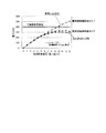
次に、本実施例の作用について図2乃至図4も参照して説明する。図2は、保護機能部13が保護動作を行なうために用いるデータテーブルであり、横軸は、入力信号として与えられる負荷印加電圧{+B−VM(−)}(V)を示し、縦軸に負荷電流I(A)を示す。例えば、負荷印加電圧を8Vに設定するようにECUより制御指令が与えられた場合、モータ(ファンモータ)3の定常電流は約15Aであり、モータ3がロックした場合に流れる過負荷電流は約40Aになるものとする。
Next, the operation of the present embodiment will be described with reference to FIGS. FIG. 2 is a data table used by the
これに対して、保護機能部13は、負荷印加電圧8Vの場合は負荷電流を33A(第1制限レベル)まで抑制する。この結果、負荷印加電圧は、過負荷時電流33Aに相当する約6.7Vまで低下する(ケース1)。
また、保護機能部13は、過電流を検出した時点から内部のタイマ(図示せず)によって計時を開始し、前記検出状態が所定時間継続した場合には、FET4をOFFしてモータ3に対する通電を停止させる(ケース2)。尚、以上の制御に関しては、従来より行っていた保護動作と同様である。
In contrast, the
Further, the
更に、保護機能部13は、過電流が流れたと判断される場合に加えて、電圧モニタ8により検出される電圧VM(−)を参照して、負荷印加電圧が0V付近(例えば、しきい値電圧2V以下)に低下する異常状態を検出すると、元々の指令された負荷印加電圧にかかわらず、負荷電流値を15A(第2制限レベル)まで低下させるように更に制限する(ケース3)。そして、この場合も、ケース2と同様に、過電流を検出した時点から所定時間が経過した場合には、FET4をOFFしてモータ3に対する通電を停止させる(ケース4)。
Further, the
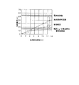
図3(a)〜(c)は、上記ケース1,2に対応する負荷電流,負荷印加電圧の変化と制御状態とを示すものであり、図3(d)〜(f)は、上記ケース3,4に対応するものである。図3(c),(f)は、条件Aが過電流検出(負荷異常),条件Bが負荷印加電圧異常を示しており、電流制限値を変更(第1→第2)する条件Cは、条件A,Bの論理積で成立させることを示している。
即ち、負荷印加電圧が0V付近に低下した場合には、モータ3の巻線がショートしたか、又は、モータ3の電源側配線が「噛み込み」などによりボディアースに落ちたような場合(後述するハイサイド駆動の場合)が想定されるので、そのような場合には、電流制限値を単なる過電流検出のケースよりも更に低く設定することで、FET4を確実に保護するようにしている。
FIGS. 3A to 3C show changes in the load current and load applied voltage corresponding to the
That is, when the load applied voltage drops to around 0 V, the winding of the
図4は、モータ3のロック時と、負荷ショートが発生した場合との消費電力をシミュレートした一例を示すものであり、バッテリ電圧+B=15V,配線抵抗を50mΩと想定している。従来と同様に過電流のみを検出して電流制限を行い負荷ショートが発生した場合には、負荷印加電圧の狙い値(ECUからの指令)が10V以上になると、FET4の保護限界領域である400Wを超えてしまう。これに対して、本実施例では、負荷ショート時の電流制限値をより低く設定することで、消費電力をモータ3のロック時と略同程度となるまで低下させることが可能となった。
FIG. 4 shows an example of simulating power consumption when the
以上のように本実施例によれば、駆動回路(通電制御手段)7による駆動時においてモータ3に流れる負荷電流を電流モニタ9により検出すると共に、負荷印加電圧を電圧モニタ8により検出し、保護機能部13は、過電流が検出されるケース1においては負荷電流が第1制限レベル以下となるように制限し、その状態に加えて、負荷印加電圧が異常判定値を下回るケース3においては、負荷電流が第2制限レベル以下となるように電流制限を行うようにした。
従って、モータ3の巻線がショートした場合の消費電力を低減して、FET4を確実に保護することが可能となる。そして、保護機能部13は、過電流の検出状態が所定時間継続するとモータ3に対する通電を停止させるので、過電流の発生状態が短時間内に解消されない場合であっても、FET4を確実に保護することができる。
As described above, according to the present embodiment, the load current flowing through the
Therefore, the power consumption when the winding of the
また、負荷駆動装置12を、車両に搭載されるファンモータ3に適用した。即ち、車両については寒冷地のような低温環境下でモータ3を駆動する場合でも正常に機能することが要求されるが、モータ3については、回転駆動する機構部部分が低温環境下で凍結して始動時にロック状態になることも想定される。そして、凍結によるロックは、モータ3のトルクを加えて解除されることも十分に期待されるため、モータ3の駆動をロック状態が検出されたことを以って直ちに停止することは望ましくない。そこで、負荷駆動装置12を適用すれば、モータ3がロックした場合でも、許容される通電状態をできる限り維持しつつFET4の保護を図るのに好適である。
The
(第2実施例)
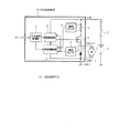
図5は本発明の第2実施例であり、第1実施例と同一部分には同一符号を付して説明を省略し、以下異なる部分についてのみ説明する。第2実施例の負荷駆動装置14は、本発明をハイサイドリニア駆動方式に適用した場合を示すものである。即ち、ヒューズ2を介したバッテリ1の正側端子とグランドとの間には、電流検出抵抗5,FET4及びモータ3の直列回路が接続されている。
そして、電圧モニタ9は、FET4のソース側、即ち、モータ3の電源側端子電圧VM(+)を検出するようになっており、駆動回路(通電制御手段)15は、FET4のゲートに駆動信号を出力する。この場合、駆動回路15は、FET4をハイサイドで駆動するため図示しない昇圧回路を内蔵しており、その昇圧電圧をFET4のゲートに印加するように構成されている。
(Second embodiment)
FIG. 5 shows a second embodiment of the present invention. The same parts as those of the first embodiment are denoted by the same reference numerals and the description thereof is omitted. Only the different parts will be described below. The
The voltage monitor 9 detects the source side of the
このようなハイサイド駆動においては、第1実施例におけるモータ3の巻線がショートするケースに加えて、例えば、作業者がメンテナンスや修理などの作業を行った場合に、モータ3の電源側(VM(+)側)配線を機構部に挟み込んだり、又はボルトの締め付け時に配線を巻き込むなどして車両のボディアースに落としてしまういわゆる「噛み込み」が発生するおそれがある。その場合にも、巻線がショートするケースと同様の大きな電流がFET4に流れてしまう。従って、ハイサイド駆動方式の負荷駆動装置14に本発明を適用すれば、配線の噛み込みが発生した場合にもFET4を保護することができる。
以上のように構成された第2実施例によれば、モータ3をハイサイドリニア駆動する構成についても、第1実施例と同様の効果が得られる。
In such a high-side drive, in addition to the case where the winding of the
According to the second embodiment configured as described above, the same effect as that of the first embodiment can be obtained with respect to the configuration in which the
(第3実施例)
図6及び図7は本発明の第3実施例であり、第1実施例と同一部分には同一符号を付して説明を省略し、以下異なる部分についてのみ説明する。第3実施例の負荷駆動装置16は、本発明をロウサイドパルス(PWM)駆動方式に適用した場合を示すものである。即ち、モータ3には、フライホイールダイオード17が並列に接続されており、駆動回路(通電制御手段)18は、入力信号処理部6を介して与えられる制御信号に応じたデューティのPWM信号を生成してFET4に出力し、FET4は、そのPWM信号に応じてスイッチングを行う。
(Third embodiment)
6 and 7 show a third embodiment of the present invention. The same parts as those of the first embodiment are denoted by the same reference numerals, and the description thereof is omitted. Only different parts will be described below. The load driving device 16 of the third embodiment shows a case where the present invention is applied to a low side pulse (PWM) driving method. That is, the
図7は、パルス駆動時における電流制限の設定を示すものである。パルス駆動時では、過電流検出時における電流制限値(第1制限レベル)は、負荷印加電圧にかかわらず一定の53A程度とする。即ち、パルス駆動の場合は、モータ3がロックした場合の消費電力がリニア駆動の場合に比較して小さいというメリットがあるので(一方、リニア駆動にはノイズレベルが小さいというメリットがある)、電流制限値をより高く設定しておく。前述したように、寒冷地などで発生するモータ3の凍結ロック状態をブレイクするには、できるだけ大きなトルクを発生させた方が有利だからである。また、第2制限レベルについては、第1実施例と同様である。
以上のように構成された第3実施例によれば、モータ3をロウサイドパルス駆動する構成についても、第1実施例と同様の効果が得られる。
FIG. 7 shows the setting of the current limit during pulse driving. During pulse driving, the current limit value (first limit level) at the time of overcurrent detection is set to a constant value of about 53 A regardless of the load applied voltage. That is, in the case of pulse driving, there is a merit that the power consumption when the
According to the third embodiment configured as described above, the same effect as that of the first embodiment can be obtained with respect to the configuration in which the
(第4実施例)
図8は本発明の第4実施例であり、第2,第3実施例と同一部分には同一符号を付して説明を省略し、以下異なる部分についてのみ説明する。第4実施例の負荷駆動装置19は、本発明をハイサイドパルス駆動方式に適用した場合を示すものである。即ち、モータ3には、フライホイールダイオード17が並列に接続されており、駆動回路(通電制御手段)20は、入力信号処理部6を介して与えられる制御信号に応じたデューティのPWM信号を生成してFET4に出力し、FET4は、そのPWM信号に応じてスイッチング動作する。
以上のように構成された第4実施例によれば、モータ3をハイサイドパルス駆動する構成についても、第1,第2実施例と同様の効果が得られる。
(Fourth embodiment)
FIG. 8 shows a fourth embodiment of the present invention. The same parts as those of the second and third embodiments are denoted by the same reference numerals and the description thereof is omitted. Only different parts will be described below. The load driving device 19 of the fourth embodiment shows a case where the present invention is applied to a high side pulse driving system. In other words, the
According to the fourth embodiment configured as described above, the same effect as in the first and second embodiments can be obtained with respect to the configuration in which the
(第5実施例)
図9乃至図11は本発明の第5実施例を示すものである。第5実施例は、例えば第1実施例における保護機能部13の内部構成をより詳細に示したものである。図11は、参考のため、図14に示す従来技術に対応した構成を示す。即ち、駆動回路7,保護機能部10は、内部に夫々オペアンプ7a,コンパレータ10aを備えており、オペアンプ7aの反転入力端子には、入力信号処理部6によって出力されるF/V変換されたレベル信号(VMの狙い値)即ち駆動指令信号が直接与えられており、コンパレータ10aの反転入力端子には、駆動指令信号が分圧抵抗10b及び10cにより分圧されて与えられている。
また、オペアンプ7aの非反転入力端子には電圧モニタ8の出力信号が与えられており、出力端子はFET4のゲートに接続されている。即ち、オペアンプ7aは、入力信号処理部6からのレベル信号と、電圧モニタ8の出力信号との差に応じたゲート電圧をFET4のゲートに出力する。
(5th Example)
9 to 11 show a fifth embodiment of the present invention. The fifth embodiment, for example, shows the internal configuration of the
The output signal of the voltage monitor 8 is given to the non-inverting input terminal of the
そして、オペアンプ7aの出力端子には、NPNトランジスタ7bのコレクタが接続されており、そのトランジスタ7bのエミッタはグランドに接続され、ベースはコンパレータ10aの出力端子に接続されている。即ち、保護機能部10は、入力信号処理部6からの駆動指令信号に基づいて過電流しきい値を作り、電流モニタ9により検出される負荷電流値がしきい値を超えた場合はトランジスタ7bをオンさせてFETのゲートレベルをグランドに設定し、モータ3への通電を停止させるようになっている。
尚、トランジスタ7bの作用により通電が停止されると、電流モニタ9によって検出される抵抗5の端子電圧は低下してコンパレータ10aの出力レベルはロウに戻る。従って、過電流状態がある期間継続する場合はトランジスタ7bはオンオフを繰り返すことになり、その結果として所定の電流制限レベルが定まるようになる。
The output terminal of the
When the energization is stopped by the action of the
図9は、第1実施例の保護機能部13に対応する構成である。保護機能部13は、4つのコンパレータ13a〜13d(CP1〜CP4)を備えている。コンパレータ13a並びに分圧抵抗13f,13gは、図11に示す保護機能部10の構成と同様の作用をなすものであり、過電流検出時に第1制限レベルによる電流制限動作を行なう(図10,CP1参照)。コンパレータ13bの反転入力端子には、一定のしきい値電圧が与えられており、モータ電圧VM及びモータ電流IMが低い領域における制限レベル及び負荷ショート検出時の第2制限レベルを与える(図10,CP2参照)。
FIG. 9 shows a configuration corresponding to the
コンパレータ13aの出力端子はANDゲート13iの一方の入力端子に接続されており、ANDゲート13iの他方の入力端子には、コンパレータ13bの出力端子が接続されている。そして、ANDゲート13iの出力端子は、トランジスタ7bのベースに接続されている。
コンパレータ13cの反転入力端子には、電圧モニタ8の出力電圧を分圧する抵抗13j及び13kの分圧点が接続されており、非反転入力端子には電流モニタ9の出力電圧が与えられている。即ち、コンパレータ13cは、これらの入力に基づいて過電流判定(負荷異常判定)を行う。一方、コンパレータ13dの反転入力端子には、電圧モニタ8の出力電圧が直接与えられており、非反転入力端子には一定の負荷ショート判定電圧が与えられている。即ち、コンパレータ13dは、これらの入力に基づいて負荷ショート判定を行う。そして、コンパレータ13c,13dの出力端子は、ANDゲート13lの入力端子に夫々接続されており、ANDゲート13lの出力端子は、NPNトランジスタ13mのベースに接続されている。トランジスタ13mのコレクタは、駆動指令信号線(F/V)に接続されており、エミッタはグランドに接続されている。
The output terminal of the
A voltage dividing point of
次に、保護機能部13の回路動作を説明する。駆動指令信号のレベルが低く、モータ電圧VM及びモータ電流IMが低い領域(しきい値:CP1<CP2)においては、コンパレータ13a側の出力は常にハイレベルとなり、コンパレータ13b側の一定のしきい値が有効となる。また、駆動指令信号のレベルが上昇し、モータ電圧VM及びモータ電流IMが高くなる領域(しきい値:CP1≧CP2)においてはコンパレータ13bがハイレベルを出力し続けることでコンパレータ13a側のしきい値が有効となり、電流制限レベルはリニアに上昇する。
そして、コンパレータ13cが過電流を検出すると共にコンパレータ13dが負荷ショートを検出した場合は、ANDゲート13lがハイレベルを出力してトランジスタ13mをオンさせる。すると、コンパレータ13a側のしきい値はグランドレベルに低下するため、コンパレータ13a側の出力は常にハイレベルとなり、コンパレータ13b側の一定のしきい値が有効となる。その結果、図2に示すような電流制限動作が行なわれる。
Next, the circuit operation of the
When the
(第6実施例)
図12は本発明の第6実施例を示すものである。第6実施例の負荷駆動装置21は、例えば第1実施例における保護機能部13を保護機能部(電流検出手段)22に置き換えたものであり、図12は、保護機能部22の内部構成の一部分を示す。即ち、上記第1乃至第5実施例では、何れも過電流を検出すると共に、負荷に対する印加電圧がしきい値電圧以下になると通電電流量を第2制限レベル以下に制限している。
しかしながら、斯様な構成の場合、電流や電圧のしきい値を設定するに当たっては、大電流が流れることで配線抵抗による電圧降下分などを考慮する必要がある。そのため、異常発生時においてFET4に生じる消費電力の制御が難しく、しきい値に与えるマージンの設定が困難であるという問題がある。また、システム毎にしきい値の設定が必要となり、製品のバリエーションが増加するという問題もある。
(Sixth embodiment)
FIG. 12 shows a sixth embodiment of the present invention. The
However, in the case of such a configuration, it is necessary to consider a voltage drop due to wiring resistance due to the flow of a large current when setting the current and voltage thresholds. Therefore, there is a problem that it is difficult to control power consumption generated in the
そこで、第6実施例では、電圧モニタ8によって検出されるモータ電圧VMを、抵抗23及び24により分圧し、その分圧電位V1をコンパレータ25の反転入力端子に与える。また、コンパレータ25の非反転入力端子には、電流モニタ9の検出電圧V2を与え、V2>V1となった場合に、コンパレータ25がハイレベルの異常検出信号を出力するように構成する。このコンパレータ25は、第5実施例におけるコンパレータ13dに置き換わるものである。
Therefore, in the sixth embodiment, the motor voltage VM detected by the voltage monitor 8 is divided by the
ここで、抵抗23,24の抵抗値を夫々R1,R2とし、電流検出抵抗5の抵抗値をRLとすると、モータ3の抵抗RMは、負荷電流をIMとすれば、
RM=VM/IM
である。そして、
V1=VM・R2/(R1+R2),V2=RL・IM
であるから、電圧V1,V2が等しくなる場合は、
VM・R2/(R1+R2)=RL・IM
RM=VM/IM=RL・(R1+R2)/R2
として、負荷抵抗値RMが求められる。
従って、判定対象とする負荷抵抗値RMに対して、抵抗値R1,R2を上式の関係に設定すれば、モータ3の負荷抵抗値RMに基づく検出を行なうことができる。即ち、V2>V1となった場合は、負荷抵抗値RMが低下したことを意味するので、コンパレータ25の出力信号によってモータ3の異常を検出することができる。そして、この異常は第1実施例における通電電流の第2制限レベルに対応する。
Here, if the resistance values of the
RM = VM / IM
It is. And
V1 = VM.R2 / (R1 + R2), V2 = RL.IM
Therefore, when the voltages V1 and V2 are equal,
VM · R2 / (R1 + R2) = RL · IM
RM = VM / IM = RL. (R1 + R2) / R2
As a result, a load resistance value RM is obtained.
Therefore, if the resistance values R1 and R2 are set in the above relation with respect to the load resistance value RM to be determined, detection based on the load resistance value RM of the
以上のように第6実施例によれば、保護機能部22は、電流モニタ9によって検出される電流と電圧モニタ8によって検出される電圧とに基づいて得られるモータ3の抵抗値RMがしきい値を下回ると、モータ3に流れる電流IMが第2制限レベル以下となるように制限するので、配線抵抗による電圧降下分等を考慮してしきい値を設定する必要がなくなる。従って、モータ3の印加電圧VMを直接検出する場合に比較してしきい値の設定を容易に行うことができる。
そして、保護機能部22を、具体的には、電流検出抵抗5に負荷電流が流れた場合の端子電圧と、電圧モニタ8によって検出される電圧VMを抵抗分圧した電位とをコンパレータ25によって比較し、前者が後者を上回った場合に第2制限レベルによる電流制限動作を行う構成としたので、抵抗しきい値を、電流検出抵抗5並びに分圧抵抗23,24の抵抗比によって簡単に設定することができる。
As described above, according to the sixth embodiment, the
The
(第7実施例)
図13は本発明の第7実施例を示すものである。第7実施例は、第6実施例と同様の構成を、第2実施例のハイサイド駆動方式に適用した場合である。この場合も、第6実施例と全く同様に異常検出動作を行なうことができる。
(Seventh embodiment)
FIG. 13 shows a seventh embodiment of the present invention. The seventh embodiment is a case where the same configuration as that of the sixth embodiment is applied to the high-side drive system of the second embodiment. Also in this case, the abnormality detection operation can be performed in the same manner as in the sixth embodiment.
本発明は上記し又は図面に記載した実施例にのみ限定されるものではなく、次のような変形または拡張が可能である。
過電流検出状態が所定時間継続した場合に、モータ3の駆動を停止する制御については、必要に応じて実施すれば良い。
ハイサイド駆動を行う場合は、PチャネルMOSFETを用いても良い。
パルス駆動方式の場合は、FETのON電圧{(ON抵抗)×(負荷電流)}を利用して電流検出を行っても良い。
半導体素子は、MOSFETに限ることなく、バイポーラトランジスタやIGBTであっても良い。
負荷はDCモータ3に限ることなく、半導体素子により通電が行われて駆動されるものであれば適用が可能である。
The present invention is not limited to the embodiments described above or shown in the drawings, and the following modifications or expansions are possible.
The control for stopping the driving of the
When performing high-side driving, a P-channel MOSFET may be used.
In the case of the pulse drive method, current detection may be performed using the ON voltage {(ON resistance) × (load current)} of the FET.
The semiconductor element is not limited to a MOSFET, but may be a bipolar transistor or an IGBT.
The load is not limited to the
第3,第4実施例において、入力信号処理部6より保護機能部13に駆動指令信号を与えずに、電流制限のしきい値を一定に設定しても良い。即ち、パルス駆動方式の場合は、負荷電流が比較的小さいからである。
第6,第7実施例における負荷抵抗値RMを検出して負荷電流を第2制限レベルにする構成を、異なる抵抗しきい値を設定したコンパレータをもう1つ設けることで、第1制限レベルをかける構成にも適用して良い。また、第6,第7実施例のコンパレータ25のみによって電流制限動作を行っても良い。
車載用に限ることなく、半導体素子を過電流より保護する必要があるものであれば、広く適用することができる。
In the third and fourth embodiments, the input
In the sixth and seventh embodiments, the load resistance value RM is detected and the load current is set to the second limit level. By providing another comparator having different resistance thresholds, the first limit level is set. You may apply also to the structure which applies. Further, the current limiting operation may be performed only by the
The present invention is not limited to in-vehicle use and can be widely applied as long as it is necessary to protect a semiconductor element from overcurrent.
図面中、3はモータ(負荷)、4はNチャネルMOSFET(半導体素子)、5は電流検出抵抗(電流検出手段)、7は駆動回路(通電制御手段)、8は電圧モニタ(電圧検出手段)、9は電流モニタ(電流検出手段)、12は負荷駆動装置、13は保護機能部(電流制限手段)、14は負荷駆動装置、15は駆動回路(通電制御手段)、16は負荷駆動装置、18は駆動回路(通電制御手段)、19は負荷駆動装置、20は駆動回路(通電制御手段)、21は負荷駆動装置、22は保護機能部(電流制限手段)、23,24は分圧抵抗、25はコンパレータを示す。
In the drawings, 3 is a motor (load), 4 is an N-channel MOSFET (semiconductor element), 5 is a current detection resistor (current detection means), 7 is a drive circuit (energization control means), and 8 is a voltage monitor (voltage detection means). , 9 is a current monitor (current detection means), 12 is a load drive device, 13 is a protection function unit (current limiting means), 14 is a load drive device, 15 is a drive circuit (energization control means), 16 is a load drive device, 18 is a drive circuit (energization control means), 19 is a load drive device, 20 is a drive circuit (energization control means), 21 is a load drive device, 22 is a protection function unit (current limiting means), and 23 and 24 are voltage dividing resistors. , 25 indicate comparators.
Claims (10)
前記負荷に流れる電流を検出する電流検出手段と、
前記負荷に対して印加される電圧を検出する電圧検出手段と、
前記電流検出手段によって検出される電流がしきい値を超えると前記負荷に流れる電流が第1制限レベル以下となるように制限し、前記検出電流がしきい値を超えると共に前記電圧検出手段によって検出される電圧がしきい値を下回ると、前記負荷に流れる電流が、前記第1制限レベルよりも低く設定される第2制限レベル以下となるように電流制限を行う電流制限手段とを備えることを特徴とする負荷駆動装置。 Energization control means for energizing the load by controlling semiconductor elements connected in series to the load;
Current detection means for detecting a current flowing through the load;
Voltage detecting means for detecting a voltage applied to the load;
When the current detected by the current detection means exceeds a threshold value, the current flowing through the load is limited to be equal to or lower than a first limit level, and the detection current exceeds the threshold value and is detected by the voltage detection means. When the voltage falls below a threshold that is, the current flowing through the load, be provided with a pre-SL current limiting means for performing the current limit such that the second limit level below which is set lower than the first limit level A load driving device characterized by the above.
前記電流制限手段は、前記端子電圧と、前記電圧検出手段によって検出される電圧を抵抗分圧した電位とを比較し、前者が後者を上回った場合に前記第2制限レベルによる電流制限動作を行うように構成されていることを特徴とする請求項1記載の負荷駆動装置。 The current detection means is configured to detect a terminal voltage when the load current flows through a detection resistor,
The current limiting means compares the terminal voltage with a potential obtained by resistance-dividing the voltage detected by the voltage detecting means, and performs a current limiting operation based on the second limit level when the former exceeds the latter. The load driving device according to claim 1 , wherein the load driving device is configured as described above.
前記負荷に通電を行う場合、前記負荷に流れる電流を検出すると共に前記負荷に対して印加される電圧を検出し、
前記検出電流がしきい値を超えると前記負荷に流れる電流が第1制限レベル以下となるように制限し、
前記検出電流がしきい値を超えると共に前記検出電圧がしきい値を下回ると、前記負荷に流れる電流が、前記第1制限レベルよりも低く設定される第2制限レベル以下となるように電流制限を行なう負荷駆動制御方法。 Control the semiconductor elements connected in series with the load,
When energizing the load, the current flowing through the load is detected and the voltage applied to the load is detected,
When the detected current exceeds a threshold, the current flowing through the load is limited to be equal to or lower than a first limit level,
Wherein when the detection voltage falls below the threshold value with the detected current exceeds the threshold, the current flowing through the load, before Symbol second limit level or less become as current set lower than the first limit level Load drive control method for limiting.
前記端子電圧と前記検出電圧を抵抗分圧した電位とを比較して、前者が後者を上回った場合に前記第2制限レベルによる電流制限動作を行うことを特徴とする請求項6記載の負荷駆動制御方法。 Detect the terminal voltage when the load current flows through the detection resistor,
The load drive according to claim 6, wherein the terminal voltage is compared with a potential obtained by resistance-dividing the detection voltage, and when the former exceeds the latter, a current limiting operation is performed according to the second limit level. Control method.
Priority Applications (2)
| Application Number | Priority Date | Filing Date | Title |
|---|---|---|---|
| JP2004354232A JP4529666B2 (en) | 2004-03-03 | 2004-12-07 | Load drive device and load drive control method |
| US11/067,735 US7154240B2 (en) | 2004-03-03 | 2005-03-01 | Load-driving device and method of driving load |
Applications Claiming Priority (2)
| Application Number | Priority Date | Filing Date | Title |
|---|---|---|---|
| JP2004059026 | 2004-03-03 | ||
| JP2004354232A JP4529666B2 (en) | 2004-03-03 | 2004-12-07 | Load drive device and load drive control method |
Publications (3)
| Publication Number | Publication Date |
|---|---|
| JP2005287284A JP2005287284A (en) | 2005-10-13 |
| JP2005287284A5 JP2005287284A5 (en) | 2009-05-21 |
| JP4529666B2 true JP4529666B2 (en) | 2010-08-25 |
Family
ID=34914502
Family Applications (1)
| Application Number | Title | Priority Date | Filing Date |
|---|---|---|---|
| JP2004354232A Expired - Fee Related JP4529666B2 (en) | 2004-03-03 | 2004-12-07 | Load drive device and load drive control method |
Country Status (2)
| Country | Link |
|---|---|
| US (1) | US7154240B2 (en) |
| JP (1) | JP4529666B2 (en) |
Families Citing this family (24)
| Publication number | Priority date | Publication date | Assignee | Title |
|---|---|---|---|---|
| US20070160481A1 (en) * | 2006-01-11 | 2007-07-12 | Fan-Tastic Vent | Control scheme for a roof vent fan assembly |
| DE102005011578A1 (en) * | 2005-03-14 | 2006-09-21 | Robert Bosch Gmbh | Method and circuit arrangement for limiting the current consumption of a DC motor |
| JP4765779B2 (en) * | 2005-07-19 | 2011-09-07 | 株式会社デンソー | Control device, short detection device, load drive system and program |
| JP2007060762A (en) * | 2005-08-23 | 2007-03-08 | Mitsubishi Electric Corp | Device for detecting fault of load driving system |
| US20070184775A1 (en) * | 2006-02-08 | 2007-08-09 | Perkins Bernard L | Remote control ventilator system and method |
| WO2008077439A1 (en) * | 2006-12-22 | 2008-07-03 | Freescale Semiconductor, Inc. | Power supply switching apparatus with severe overload detection |
| JP4469886B2 (en) | 2007-09-20 | 2010-06-02 | 日立オートモティブシステムズ株式会社 | Load drive circuit |
| JP2012090493A (en) * | 2010-10-22 | 2012-05-10 | Sanyo Electric Co Ltd | Motor drive device and projection-type display device |
| US8878475B2 (en) * | 2010-11-05 | 2014-11-04 | Stmicroelectronics, Inc. | Current limiting for a motor winding |
| JP5195897B2 (en) * | 2010-12-27 | 2013-05-15 | 株式会社デンソー | Electric load drive |
| JP5195896B2 (en) * | 2010-12-27 | 2013-05-15 | 株式会社デンソー | Electric load drive |
| IT1404251B1 (en) * | 2011-01-25 | 2013-11-15 | Gate Srl | CONTROL DEVICE FOR A DIRECT CURRENT ELECTRIC MOTOR OF A COOLING FAN FOR MOTOR VEHICLES |
| JP5750311B2 (en) * | 2011-05-31 | 2015-07-22 | 日立オートモティブシステムズ株式会社 | Inverter drive |
| KR101360436B1 (en) * | 2011-12-09 | 2014-02-12 | 기아자동차주식회사 | Pulse width modulation controller |
| DE102012005950A1 (en) * | 2012-01-17 | 2013-07-18 | W.E.T. Automotive Systems Ag | Method for controlling a fan |
| CN103206394B (en) * | 2012-01-17 | 2015-10-28 | 捷温汽车系统(中国)有限公司 | Control the method for fan |
| JP5840975B2 (en) * | 2012-02-22 | 2016-01-06 | 三菱電機株式会社 | Gate drive circuit |
| JP5889723B2 (en) * | 2012-06-07 | 2016-03-22 | ルネサスエレクトロニクス株式会社 | Semiconductor device |
| JP5860362B2 (en) * | 2012-08-22 | 2016-02-16 | 日本特殊陶業株式会社 | Load drive device |
| DE102013208982A1 (en) | 2013-05-15 | 2014-11-20 | Zf Friedrichshafen Ag | Circuit and method for controlling a current for an electromechanical load |
| US9608428B2 (en) * | 2014-01-20 | 2017-03-28 | Infineon Technologies Austria Ag | Distinguishing between overload and open load in off conditions |
| WO2015118772A1 (en) * | 2014-02-06 | 2015-08-13 | 日立オートモティブシステムズ株式会社 | Load drive circuit |
| CN107453654A (en) * | 2016-06-01 | 2017-12-08 | 德昌电机(深圳)有限公司 | Fan and its motor driver |
| DE102017127752A1 (en) * | 2017-11-23 | 2019-05-23 | Infineon Technologies Ag | METHOD AND ELECTRONIC SWITCHING FOR CONTROLLING A TRANSISTOR CONSTRUCTION ELEMENT |
Citations (3)
| Publication number | Priority date | Publication date | Assignee | Title |
|---|---|---|---|---|
| JPH04351491A (en) * | 1991-05-27 | 1992-12-07 | Nippondenso Co Ltd | Controller for motor |
| JPH05137370A (en) * | 1991-11-08 | 1993-06-01 | Nippondenso Co Ltd | Motor controller |
| JP2000333482A (en) * | 1999-03-18 | 2000-11-30 | Denso Corp | Motor drive |
Family Cites Families (8)
| Publication number | Priority date | Publication date | Assignee | Title |
|---|---|---|---|---|
| US4270164A (en) * | 1979-02-28 | 1981-05-26 | Contraves Goerz Corporation | Short circuit protection for switching type power processors |
| US4628235A (en) * | 1985-09-19 | 1986-12-09 | Gulf & Western Manufacturing Company | Control circuit for motor driver |
| FR2637732B1 (en) | 1988-10-07 | 1995-11-17 | Gen Electric Cgr | IMPROVEMENTS ON X-RAY TUBE COOLING DEVICES |
| US5192901A (en) * | 1990-03-16 | 1993-03-09 | Cherry Semiconductor Corporation | Short circuit protection |
| DE69217280T2 (en) * | 1991-07-10 | 1997-05-28 | Koyo Seiko Co | Steering with an electric assistant |
| US6170241B1 (en) * | 1996-04-26 | 2001-01-09 | Tecumseh Products Company | Microprocessor controlled motor controller with current limiting protection |
| US6545513B2 (en) * | 2001-05-17 | 2003-04-08 | Denso Corporation | Electric load drive apparatus |
| JP3767445B2 (en) * | 2001-09-28 | 2006-04-19 | アンデン株式会社 | Power supply device having overcurrent protection function, load drive device, and vehicle power supply device |
-
2004
- 2004-12-07 JP JP2004354232A patent/JP4529666B2/en not_active Expired - Fee Related
-
2005
- 2005-03-01 US US11/067,735 patent/US7154240B2/en active Active
Patent Citations (3)
| Publication number | Priority date | Publication date | Assignee | Title |
|---|---|---|---|---|
| JPH04351491A (en) * | 1991-05-27 | 1992-12-07 | Nippondenso Co Ltd | Controller for motor |
| JPH05137370A (en) * | 1991-11-08 | 1993-06-01 | Nippondenso Co Ltd | Motor controller |
| JP2000333482A (en) * | 1999-03-18 | 2000-11-30 | Denso Corp | Motor drive |
Also Published As
| Publication number | Publication date |
|---|---|
| US20050194998A1 (en) | 2005-09-08 |
| JP2005287284A (en) | 2005-10-13 |
| US7154240B2 (en) | 2006-12-26 |
Similar Documents
| Publication | Publication Date | Title |
|---|---|---|
| JP4529666B2 (en) | Load drive device and load drive control method | |
| US7759891B2 (en) | Apparatus and method for detecting abnormal conditions of a motor | |
| JP3966194B2 (en) | Motor control device | |
| US20240113707A1 (en) | Switch device | |
| US6747432B2 (en) | Drive apparatus for cooling fan motor for use in vehicle | |
| US7245163B2 (en) | Overcurrent limiting controller | |
| EP3367568B1 (en) | Semiconductor device and electronic control system having the same | |
| US7205737B1 (en) | Systems and methods of monitoring a motor load | |
| JP2008289048A (en) | Semiconductor element driver circuit | |
| US11038341B2 (en) | Load driving device | |
| JP2001298988A (en) | Motor drive | |
| JP2011078228A (en) | Overcurrent protection circuit | |
| US9391603B2 (en) | Semiconductor device, electronic appliance, and vehicle | |
| JP2010104079A (en) | Load driver | |
| US7499253B2 (en) | Semiconductor integrated-circuit unit with temperature protective circuit | |
| JP3966099B2 (en) | Electric load drive | |
| JP2004178967A (en) | Relay control device | |
| US6323611B1 (en) | Circuit for operating an electric motor | |
| JP2000308250A (en) | Controller and method for power supplying | |
| US11581887B2 (en) | Overcurrent protection circuit | |
| JP2008228371A (en) | Drive controller of electric motor for vehicle | |
| JP2004268766A (en) | Air conditioner for vehicle | |
| KR200383028Y1 (en) | A driving control apparatus for car cooperation blower motor be possessed of trouble diagnosis function | |
| JP2005069160A (en) | Motor-driven fan control device | |
| JP2012026359A (en) | Fuel pump control device |
Legal Events
| Date | Code | Title | Description |
|---|---|---|---|
| A621 | Written request for application examination |
Free format text: JAPANESE INTERMEDIATE CODE: A621 Effective date: 20061222 |
|
| A521 | Written amendment |
Free format text: JAPANESE INTERMEDIATE CODE: A523 Effective date: 20090406 |
|
| A131 | Notification of reasons for refusal |
Free format text: JAPANESE INTERMEDIATE CODE: A131 Effective date: 20090728 |
|
| A131 | Notification of reasons for refusal |
Free format text: JAPANESE INTERMEDIATE CODE: A131 Effective date: 20091215 |
|
| TRDD | Decision of grant or rejection written | ||
| A01 | Written decision to grant a patent or to grant a registration (utility model) |
Free format text: JAPANESE INTERMEDIATE CODE: A01 Effective date: 20100518 |
|
| A01 | Written decision to grant a patent or to grant a registration (utility model) |
Free format text: JAPANESE INTERMEDIATE CODE: A01 |
|
| A61 | First payment of annual fees (during grant procedure) |
Free format text: JAPANESE INTERMEDIATE CODE: A61 Effective date: 20100531 |
|
| R151 | Written notification of patent or utility model registration |
Ref document number: 4529666 Country of ref document: JP Free format text: JAPANESE INTERMEDIATE CODE: R151 |
|
| FPAY | Renewal fee payment (event date is renewal date of database) |
Free format text: PAYMENT UNTIL: 20130618 Year of fee payment: 3 |
|
| FPAY | Renewal fee payment (event date is renewal date of database) |
Free format text: PAYMENT UNTIL: 20140618 Year of fee payment: 4 |
|
| R250 | Receipt of annual fees |
Free format text: JAPANESE INTERMEDIATE CODE: R250 |
|
| R250 | Receipt of annual fees |
Free format text: JAPANESE INTERMEDIATE CODE: R250 |
|
| R250 | Receipt of annual fees |
Free format text: JAPANESE INTERMEDIATE CODE: R250 |
|
| R250 | Receipt of annual fees |
Free format text: JAPANESE INTERMEDIATE CODE: R250 |
|
| R250 | Receipt of annual fees |
Free format text: JAPANESE INTERMEDIATE CODE: R250 |
|
| R250 | Receipt of annual fees |
Free format text: JAPANESE INTERMEDIATE CODE: R250 |
|
| R250 | Receipt of annual fees |
Free format text: JAPANESE INTERMEDIATE CODE: R250 |
|
| LAPS | Cancellation because of no payment of annual fees |