JP4507582B2 - Mounting method of electronic components with bumps - Google Patents
Mounting method of electronic components with bumps Download PDFInfo
- Publication number
- JP4507582B2 JP4507582B2 JP2003414476A JP2003414476A JP4507582B2 JP 4507582 B2 JP4507582 B2 JP 4507582B2 JP 2003414476 A JP2003414476 A JP 2003414476A JP 2003414476 A JP2003414476 A JP 2003414476A JP 4507582 B2 JP4507582 B2 JP 4507582B2
- Authority
- JP
- Japan
- Prior art keywords
- electronic component
- metal
- electrode
- bump
- substrate
- Prior art date
- Legal status (The legal status is an assumption and is not a legal conclusion. Google has not performed a legal analysis and makes no representation as to the accuracy of the status listed.)
- Expired - Lifetime
Links
- 238000000034 method Methods 0.000 title claims description 34
- 239000002184 metal Substances 0.000 claims description 78
- 229910052751 metal Inorganic materials 0.000 claims description 78
- 239000000758 substrate Substances 0.000 claims description 27
- 229920005989 resin Polymers 0.000 claims description 25
- 239000011347 resin Substances 0.000 claims description 25
- PCHJSUWPFVWCPO-UHFFFAOYSA-N gold Chemical compound [Au] PCHJSUWPFVWCPO-UHFFFAOYSA-N 0.000 claims description 14
- 239000010931 gold Substances 0.000 claims description 14
- 229910052737 gold Inorganic materials 0.000 claims description 14
- 229920001187 thermosetting polymer Polymers 0.000 claims description 10
- 238000003825 pressing Methods 0.000 description 19
- 238000010438 heat treatment Methods 0.000 description 5
- ATJFFYVFTNAWJD-UHFFFAOYSA-N Tin Chemical compound [Sn] ATJFFYVFTNAWJD-UHFFFAOYSA-N 0.000 description 1
- 238000002788 crimping Methods 0.000 description 1
- 230000003111 delayed effect Effects 0.000 description 1
- 238000010586 diagram Methods 0.000 description 1
- 238000006073 displacement reaction Methods 0.000 description 1
- 230000000694 effects Effects 0.000 description 1
- 239000003822 epoxy resin Substances 0.000 description 1
- 150000002739 metals Chemical class 0.000 description 1
- 239000004033 plastic Substances 0.000 description 1
- 238000007747 plating Methods 0.000 description 1
- 229920000647 polyepoxide Polymers 0.000 description 1
- 239000004065 semiconductor Substances 0.000 description 1
Images


Classifications
-
- H—ELECTRICITY
- H01—ELECTRIC ELEMENTS
- H01L—SEMICONDUCTOR DEVICES NOT COVERED BY CLASS H10
- H01L24/00—Arrangements for connecting or disconnecting semiconductor or solid-state bodies; Methods or apparatus related thereto
- H01L24/80—Methods for connecting semiconductor or other solid state bodies using means for bonding being attached to, or being formed on, the surface to be connected
- H01L24/81—Methods for connecting semiconductor or other solid state bodies using means for bonding being attached to, or being formed on, the surface to be connected using a bump connector
-
- B—PERFORMING OPERATIONS; TRANSPORTING
- B23—MACHINE TOOLS; METAL-WORKING NOT OTHERWISE PROVIDED FOR
- B23K—SOLDERING OR UNSOLDERING; WELDING; CLADDING OR PLATING BY SOLDERING OR WELDING; CUTTING BY APPLYING HEAT LOCALLY, e.g. FLAME CUTTING; WORKING BY LASER BEAM
- B23K20/00—Non-electric welding by applying impact or other pressure, with or without the application of heat, e.g. cladding or plating
- B23K20/10—Non-electric welding by applying impact or other pressure, with or without the application of heat, e.g. cladding or plating making use of vibrations, e.g. ultrasonic welding
-
- H—ELECTRICITY
- H01—ELECTRIC ELEMENTS
- H01L—SEMICONDUCTOR DEVICES NOT COVERED BY CLASS H10
- H01L21/00—Processes or apparatus adapted for the manufacture or treatment of semiconductor or solid state devices or of parts thereof
- H01L21/02—Manufacture or treatment of semiconductor devices or of parts thereof
- H01L21/04—Manufacture or treatment of semiconductor devices or of parts thereof the devices having at least one potential-jump barrier or surface barrier, e.g. PN junction, depletion layer or carrier concentration layer
- H01L21/50—Assembly of semiconductor devices using processes or apparatus not provided for in a single one of the subgroups H01L21/06 - H01L21/326, e.g. sealing of a cap to a base of a container
- H01L21/60—Attaching or detaching leads or other conductive members, to be used for carrying current to or from the device in operation
-
- H—ELECTRICITY
- H01—ELECTRIC ELEMENTS
- H01L—SEMICONDUCTOR DEVICES NOT COVERED BY CLASS H10
- H01L2224/00—Indexing scheme for arrangements for connecting or disconnecting semiconductor or solid-state bodies and methods related thereto as covered by H01L24/00
- H01L2224/01—Means for bonding being attached to, or being formed on, the surface to be connected, e.g. chip-to-package, die-attach, "first-level" interconnects; Manufacturing methods related thereto
- H01L2224/02—Bonding areas; Manufacturing methods related thereto
- H01L2224/04—Structure, shape, material or disposition of the bonding areas prior to the connecting process
- H01L2224/05—Structure, shape, material or disposition of the bonding areas prior to the connecting process of an individual bonding area
- H01L2224/0554—External layer
- H01L2224/0556—Disposition
- H01L2224/05568—Disposition the whole external layer protruding from the surface
-
- H—ELECTRICITY
- H01—ELECTRIC ELEMENTS
- H01L—SEMICONDUCTOR DEVICES NOT COVERED BY CLASS H10
- H01L2224/00—Indexing scheme for arrangements for connecting or disconnecting semiconductor or solid-state bodies and methods related thereto as covered by H01L24/00
- H01L2224/01—Means for bonding being attached to, or being formed on, the surface to be connected, e.g. chip-to-package, die-attach, "first-level" interconnects; Manufacturing methods related thereto
- H01L2224/02—Bonding areas; Manufacturing methods related thereto
- H01L2224/04—Structure, shape, material or disposition of the bonding areas prior to the connecting process
- H01L2224/05—Structure, shape, material or disposition of the bonding areas prior to the connecting process of an individual bonding area
- H01L2224/0554—External layer
- H01L2224/05573—Single external layer
-
- H—ELECTRICITY
- H01—ELECTRIC ELEMENTS
- H01L—SEMICONDUCTOR DEVICES NOT COVERED BY CLASS H10
- H01L2224/00—Indexing scheme for arrangements for connecting or disconnecting semiconductor or solid-state bodies and methods related thereto as covered by H01L24/00
- H01L2224/01—Means for bonding being attached to, or being formed on, the surface to be connected, e.g. chip-to-package, die-attach, "first-level" interconnects; Manufacturing methods related thereto
- H01L2224/02—Bonding areas; Manufacturing methods related thereto
- H01L2224/04—Structure, shape, material or disposition of the bonding areas prior to the connecting process
- H01L2224/05—Structure, shape, material or disposition of the bonding areas prior to the connecting process of an individual bonding area
- H01L2224/0554—External layer
- H01L2224/05599—Material
- H01L2224/056—Material with a principal constituent of the material being a metal or a metalloid, e.g. boron [B], silicon [Si], germanium [Ge], arsenic [As], antimony [Sb], tellurium [Te] and polonium [Po], and alloys thereof
- H01L2224/05638—Material with a principal constituent of the material being a metal or a metalloid, e.g. boron [B], silicon [Si], germanium [Ge], arsenic [As], antimony [Sb], tellurium [Te] and polonium [Po], and alloys thereof the principal constituent melting at a temperature of greater than or equal to 950°C and less than 1550°C
- H01L2224/05644—Gold [Au] as principal constituent
-
- H—ELECTRICITY
- H01—ELECTRIC ELEMENTS
- H01L—SEMICONDUCTOR DEVICES NOT COVERED BY CLASS H10
- H01L2224/00—Indexing scheme for arrangements for connecting or disconnecting semiconductor or solid-state bodies and methods related thereto as covered by H01L24/00
- H01L2224/01—Means for bonding being attached to, or being formed on, the surface to be connected, e.g. chip-to-package, die-attach, "first-level" interconnects; Manufacturing methods related thereto
- H01L2224/10—Bump connectors; Manufacturing methods related thereto
- H01L2224/12—Structure, shape, material or disposition of the bump connectors prior to the connecting process
- H01L2224/13—Structure, shape, material or disposition of the bump connectors prior to the connecting process of an individual bump connector
- H01L2224/13001—Core members of the bump connector
- H01L2224/13099—Material
- H01L2224/131—Material with a principal constituent of the material being a metal or a metalloid, e.g. boron [B], silicon [Si], germanium [Ge], arsenic [As], antimony [Sb], tellurium [Te] and polonium [Po], and alloys thereof
- H01L2224/13138—Material with a principal constituent of the material being a metal or a metalloid, e.g. boron [B], silicon [Si], germanium [Ge], arsenic [As], antimony [Sb], tellurium [Te] and polonium [Po], and alloys thereof the principal constituent melting at a temperature of greater than or equal to 950°C and less than 1550°C
- H01L2224/13144—Gold [Au] as principal constituent
-
- H—ELECTRICITY
- H01—ELECTRIC ELEMENTS
- H01L—SEMICONDUCTOR DEVICES NOT COVERED BY CLASS H10
- H01L2224/00—Indexing scheme for arrangements for connecting or disconnecting semiconductor or solid-state bodies and methods related thereto as covered by H01L24/00
- H01L2224/01—Means for bonding being attached to, or being formed on, the surface to be connected, e.g. chip-to-package, die-attach, "first-level" interconnects; Manufacturing methods related thereto
- H01L2224/10—Bump connectors; Manufacturing methods related thereto
- H01L2224/15—Structure, shape, material or disposition of the bump connectors after the connecting process
- H01L2224/16—Structure, shape, material or disposition of the bump connectors after the connecting process of an individual bump connector
-
- H—ELECTRICITY
- H01—ELECTRIC ELEMENTS
- H01L—SEMICONDUCTOR DEVICES NOT COVERED BY CLASS H10
- H01L2224/00—Indexing scheme for arrangements for connecting or disconnecting semiconductor or solid-state bodies and methods related thereto as covered by H01L24/00
- H01L2224/74—Apparatus for manufacturing arrangements for connecting or disconnecting semiconductor or solid-state bodies and for methods related thereto
- H01L2224/75—Apparatus for connecting with bump connectors or layer connectors
- H01L2224/757—Means for aligning
- H01L2224/75743—Suction holding means
-
- H—ELECTRICITY
- H01—ELECTRIC ELEMENTS
- H01L—SEMICONDUCTOR DEVICES NOT COVERED BY CLASS H10
- H01L2224/00—Indexing scheme for arrangements for connecting or disconnecting semiconductor or solid-state bodies and methods related thereto as covered by H01L24/00
- H01L2224/80—Methods for connecting semiconductor or other solid state bodies using means for bonding being attached to, or being formed on, the surface to be connected
- H01L2224/81—Methods for connecting semiconductor or other solid state bodies using means for bonding being attached to, or being formed on, the surface to be connected using a bump connector
- H01L2224/818—Bonding techniques
- H01L2224/81801—Soldering or alloying
-
- H—ELECTRICITY
- H01—ELECTRIC ELEMENTS
- H01L—SEMICONDUCTOR DEVICES NOT COVERED BY CLASS H10
- H01L2224/00—Indexing scheme for arrangements for connecting or disconnecting semiconductor or solid-state bodies and methods related thereto as covered by H01L24/00
- H01L2224/80—Methods for connecting semiconductor or other solid state bodies using means for bonding being attached to, or being formed on, the surface to be connected
- H01L2224/83—Methods for connecting semiconductor or other solid state bodies using means for bonding being attached to, or being formed on, the surface to be connected using a layer connector
- H01L2224/8319—Arrangement of the layer connectors prior to mounting
- H01L2224/83192—Arrangement of the layer connectors prior to mounting wherein the layer connectors are disposed only on another item or body to be connected to the semiconductor or solid-state body
-
- H—ELECTRICITY
- H01—ELECTRIC ELEMENTS
- H01L—SEMICONDUCTOR DEVICES NOT COVERED BY CLASS H10
- H01L24/00—Arrangements for connecting or disconnecting semiconductor or solid-state bodies; Methods or apparatus related thereto
- H01L24/01—Means for bonding being attached to, or being formed on, the surface to be connected, e.g. chip-to-package, die-attach, "first-level" interconnects; Manufacturing methods related thereto
- H01L24/02—Bonding areas ; Manufacturing methods related thereto
- H01L24/04—Structure, shape, material or disposition of the bonding areas prior to the connecting process
- H01L24/05—Structure, shape, material or disposition of the bonding areas prior to the connecting process of an individual bonding area
-
- H—ELECTRICITY
- H01—ELECTRIC ELEMENTS
- H01L—SEMICONDUCTOR DEVICES NOT COVERED BY CLASS H10
- H01L24/00—Arrangements for connecting or disconnecting semiconductor or solid-state bodies; Methods or apparatus related thereto
- H01L24/01—Means for bonding being attached to, or being formed on, the surface to be connected, e.g. chip-to-package, die-attach, "first-level" interconnects; Manufacturing methods related thereto
- H01L24/10—Bump connectors ; Manufacturing methods related thereto
- H01L24/12—Structure, shape, material or disposition of the bump connectors prior to the connecting process
- H01L24/13—Structure, shape, material or disposition of the bump connectors prior to the connecting process of an individual bump connector
-
- H—ELECTRICITY
- H01—ELECTRIC ELEMENTS
- H01L—SEMICONDUCTOR DEVICES NOT COVERED BY CLASS H10
- H01L24/00—Arrangements for connecting or disconnecting semiconductor or solid-state bodies; Methods or apparatus related thereto
- H01L24/01—Means for bonding being attached to, or being formed on, the surface to be connected, e.g. chip-to-package, die-attach, "first-level" interconnects; Manufacturing methods related thereto
- H01L24/10—Bump connectors ; Manufacturing methods related thereto
- H01L24/15—Structure, shape, material or disposition of the bump connectors after the connecting process
- H01L24/16—Structure, shape, material or disposition of the bump connectors after the connecting process of an individual bump connector
-
- H—ELECTRICITY
- H01—ELECTRIC ELEMENTS
- H01L—SEMICONDUCTOR DEVICES NOT COVERED BY CLASS H10
- H01L2924/00—Indexing scheme for arrangements or methods for connecting or disconnecting semiconductor or solid-state bodies as covered by H01L24/00
- H01L2924/01—Chemical elements
- H01L2924/01005—Boron [B]
-
- H—ELECTRICITY
- H01—ELECTRIC ELEMENTS
- H01L—SEMICONDUCTOR DEVICES NOT COVERED BY CLASS H10
- H01L2924/00—Indexing scheme for arrangements or methods for connecting or disconnecting semiconductor or solid-state bodies as covered by H01L24/00
- H01L2924/01—Chemical elements
- H01L2924/01006—Carbon [C]
-
- H—ELECTRICITY
- H01—ELECTRIC ELEMENTS
- H01L—SEMICONDUCTOR DEVICES NOT COVERED BY CLASS H10
- H01L2924/00—Indexing scheme for arrangements or methods for connecting or disconnecting semiconductor or solid-state bodies as covered by H01L24/00
- H01L2924/01—Chemical elements
- H01L2924/01033—Arsenic [As]
-
- H—ELECTRICITY
- H01—ELECTRIC ELEMENTS
- H01L—SEMICONDUCTOR DEVICES NOT COVERED BY CLASS H10
- H01L2924/00—Indexing scheme for arrangements or methods for connecting or disconnecting semiconductor or solid-state bodies as covered by H01L24/00
- H01L2924/01—Chemical elements
- H01L2924/01047—Silver [Ag]
-
- H—ELECTRICITY
- H01—ELECTRIC ELEMENTS
- H01L—SEMICONDUCTOR DEVICES NOT COVERED BY CLASS H10
- H01L2924/00—Indexing scheme for arrangements or methods for connecting or disconnecting semiconductor or solid-state bodies as covered by H01L24/00
- H01L2924/01—Chemical elements
- H01L2924/0105—Tin [Sn]
-
- H—ELECTRICITY
- H01—ELECTRIC ELEMENTS
- H01L—SEMICONDUCTOR DEVICES NOT COVERED BY CLASS H10
- H01L2924/00—Indexing scheme for arrangements or methods for connecting or disconnecting semiconductor or solid-state bodies as covered by H01L24/00
- H01L2924/01—Chemical elements
- H01L2924/01078—Platinum [Pt]
-
- H—ELECTRICITY
- H01—ELECTRIC ELEMENTS
- H01L—SEMICONDUCTOR DEVICES NOT COVERED BY CLASS H10
- H01L2924/00—Indexing scheme for arrangements or methods for connecting or disconnecting semiconductor or solid-state bodies as covered by H01L24/00
- H01L2924/01—Chemical elements
- H01L2924/01079—Gold [Au]
Description
本発明は、複数の金属バンプが形成されたバンプ付き電子部品を基板に実装するバンプ付電子部品の実装方法に関するものである。 The present invention relates a plurality of bumps electronic component metal bumps are formed on the mounting how the electronic component with bumps mounted on the substrate.
フリップチップなど半導体素子に接続用電極である金属バンプが設けられたバンプ付電子部品を基板に実装する実装方法として、超音波接合による方法が用いられている(例えば特許文献1,2参照)。この実装方法においては、バンプ付電子部品に超音波振動と熱と加圧力を作用させながらこのバンプ付電子部品を基板に対して押圧することにより、金属バンプを基板の電極に超音波接合によって金属接合し、金属バンプを電極に電気的に接続する。
ところでバンプ付電子部品に形成された金属バンプのサイズにはばらつきが存在し、上述の超音波接合においては、サイズの大きなバンプから順に電極に接触して金属接合される。そして接合過程で金属バンプが加圧力によって幾分押し潰されて全ての金属バンプが電極に金属接合されることにより、超音波接合が完了する。 By the way, there is a variation in the size of the metal bump formed on the electronic component with bump, and in the above-described ultrasonic bonding, the metal is bonded in contact with the electrode in order from the bump having the largest size. In the joining process, the metal bumps are crushed somewhat by the applied pressure, and all the metal bumps are joined to the electrodes, thereby completing the ultrasonic joining.
しかしながら、従来のバンプ付電子部品を対象とした超音波接合においては、バンプサイズの相違により金属バンプごとに超音波接合の進展度合いが異なるため、先行して金属接合が開始された金属バンプについては、下端部が既に電極に金属接合された状態で超音波振動が継続して付与される事態が発生する。そしてこのような超音波振動が過剰に付与された金属バンプには、バンプ基部に振動変位による過大な応力が生じる結果、超音波接合過程が終了した状態でバンプ基部にクラックなどのダメージが発生するという問題があった。 However, in conventional ultrasonic bonding for bumped electronic components, the progress of ultrasonic bonding differs for each metal bump due to the difference in bump size. In this state, the ultrasonic vibration is continuously applied in a state where the lower end portion is already metal-bonded to the electrode. And, in such a metal bump to which ultrasonic vibration is excessively applied, excessive stress due to vibration displacement is generated in the bump base, and as a result, damage such as a crack occurs in the bump base in a state where the ultrasonic bonding process is completed. There was a problem.
そこで本発明は、超音波接合過程におけるダメージを防止することができるバンプ付電子部品の実装方法を提供することを目的とする。 Accordingly, the present invention aims at providing an implementation how electronic bumped component can be prevented from being damaged in the ultrasonic bonding process.
本発明のバンプ付電子部品の実装方法は、複数の金属バンプが形成されたバンプ付電子部品を複数の電極が形成された基板に実装するバンプ付電子部品の実装方法であって、前記バンプ付電子部品と前記基板との間に熱硬化性の樹脂を介在させた状態で前記複数の金属バンプを前記複数の電極に位置合わせする工程と、前記バンプ付電子部品に超音波振動と熱と加圧力を作用させながらこのバンプ付電子部品を基板に対して押圧する工程と、全ての金属バンプを前記電極に接触させて電気的に接続するとともにそのうちの一部の金属バンプを前記電極に金属接合した段階で前記超音波振動を実質的に停止する工程と、前記超音波振動を実質的に停止した後も、前記バンプ付電子部品に対して熱と加圧力を継続して作用させることにより前記熱硬化性樹脂の硬化を進展させる工程を含む。 The bumped electronic component mounting method of the present invention is a bumped electronic component mounting method for mounting a bumped electronic component on which a plurality of metal bumps are formed on a substrate on which a plurality of electrodes are formed. Aligning the plurality of metal bumps with the plurality of electrodes with a thermosetting resin interposed between the electronic component and the substrate; and applying ultrasonic vibration, heat and heat to the bumped electronic component. A step of pressing the bumped electronic component against the substrate while applying pressure, and all the metal bumps are brought into contact with the electrodes to be electrically connected, and some of the metal bumps are metal-bonded to the electrodes. The step of substantially stopping the ultrasonic vibration at the stage, and after substantially stopping the ultrasonic vibration, by continuously applying heat and pressure to the electronic component with bumps, heat Comprising the step of advance the curing of the resistance resin.
本発明によれば、バンプ付電子部品に超音波振動と熱と加圧力を作用させながらこのバンプ付電子部品を基板に対して押圧する過程において、全ての金属バンプを電極に接触させて電気的に接続するとともに、そのうちの一部の金属バンプを電極に金属接合した段階で超音波振動を実質的に停止し、超音波振動を実質的に停止した後も、バンプ付電子部品に対して熱と加圧力を継続して作用させることにより熱硬化性樹脂の硬化を進展させることにより、先行して金属接合が開始した金属バンプに超音波振動が過剰に作用することに起因するダメージを防止することができる。 According to the present invention, in the process of pressing the bumped electronic component against the substrate while applying ultrasonic vibration, heat and pressure to the bumped electronic component, all the metal bumps are brought into contact with the electrodes to electrically The ultrasonic vibration is substantially stopped at the stage where some of the metal bumps are metal-bonded to the electrode, and the electronic components with bumps are heated even after the ultrasonic vibration is substantially stopped. When the Rukoto to advance the curing of the thermosetting resin by acting to continue pressure, the damage previously ultrasonic vibration to the metal bump metal bonding has been initiated due to acting excessively prevented can do.
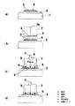
次に本発明の実施の形態を図面を参照して説明する。図1は本発明の一実施の形態の電子部品実装方法の工程説明図、図2は本発明の一実施の形態の電子部品実装構造の断面図、図3は本発明の一実施の形態の電子部品実装方法における押圧荷重と超音波出力のタイムチャートである。 Next, embodiments of the present invention will be described with reference to the drawings. 1 is a process explanatory diagram of an electronic component mounting method according to an embodiment of the present invention, FIG. 2 is a cross-sectional view of an electronic component mounting structure according to an embodiment of the present invention, and FIG. 3 is an embodiment of the present invention. It is a time chart of the pressing load and ultrasonic output in an electronic component mounting method.
まず図1を参照して、電子部品実装方法について説明する。この電子部品実装方法は、複数の金属バンプが形成されたバンプ付電子部品を、複数の電極が形成された基板に実装するものである。ここでは、金属バンプとして金を材質とする金バンプが用いられ、また電極として表面に金メッキによる金層が形成されたものを対象としている。 First, an electronic component mounting method will be described with reference to FIG. In this electronic component mounting method, an electronic component with bumps on which a plurality of metal bumps are formed is mounted on a substrate on which a plurality of electrodes are formed. Here, a gold bump made of gold is used as the metal bump, and a gold layer formed by gold plating on the surface is used as the electrode.
図1(a)において、基板保持部1には上面に電極3が形成された基板2が保持されている。基板2の上面には予めエポキシ樹脂などの熱硬化性の樹脂4がディスペンサによる塗布などの方法で供給されている。樹脂4を供給する方法としては、樹脂4をシート状にした樹脂シートを、基板2の表面に貼着するようにしてもよい。
In FIG. 1A, a
次に図1(b)に示すように、下面に接続用電極である金属バンプ6が形成されたバンプ付電子部品5(以下、単に「電子部品5」と略記)を超音波圧着用のツール7に保持させる。すなわち、電子部品5の背面(バンプ形成面の反対面)にツール7の保持面を接触させ、吸引孔7aから真空吸引することにより電子部品5を吸着保持する。
Next, as shown in FIG. 1B, a bump-equipped electronic component 5 (hereinafter simply referred to as “
ツール7が装着された圧着装置(図示省略)は、振動付与装置、加熱装置および押圧機構を備えており、電子部品5の背面にツール7を接触させた状態において、ツール7を介して電子部品5に超音波振動と熱と加圧力を作用させることができる。そしてここで振動付与装置は、超音波振動の発停および出力が任意に制御可能となっており、加熱装置は加熱温度の設定が、また押圧機構は押圧荷重の設定がそれぞれ可能となっている。
The crimping device (not shown) to which the
電子部品5を保持したツール7は、予め電極3上に樹脂4が供給された基板2上に移動する。そして電子部品5と基板2との間に樹脂4を介在させた状態で、複数の金属バンプ6を樹脂4で覆われた複数の電極3に位置合わせする。次いで図1(c)に示すように、ツール7を電子部品5ととも下降させて金属バンプ6の下端面を電極3の表面に着地させ、超音波振動(矢印a参照)と熱(矢印b参照)および加圧力(矢印c参照)によって、金属バンプ6を電極3に接合する。
The
この接合過程について、図3のタイムチャートを参照して説明する。図3は、金属バンプ6の電極3への着地が開始されるタイミングt1以降の押圧荷重および超音波出力の変化を時系列的に示したものである。なお、図3に示すタイミングの間、加熱装置はON状態にあり、ツール7による電子部品5の加熱が継続して行われる。したがって、基板2と電子部品5の間に介在する樹脂4はタイミングt1から加熱され熱硬化を開始する。
This joining process will be described with reference to the time chart of FIG. FIG. 3 shows, in a time series, changes in pressing load and ultrasonic output after timing t1 when the landing of the
ここで金属バンプ6にはサイズに多少のばらつきがあり、タイミングt1では複数の金属バンプ6のうち、サイズが相対的に大きい幾つかの金属バンプ6がまず着地する。そしてタイミングt1以降、ツール7によって電子部品5を押し下げることにより、押圧荷重が増加するとともに、当初電極3に接触した金属バンプ6はこの増加しつつある荷重によって幾分押しつぶされ、当初接触していなかった金属バンプ6が順次電極3に接触するようになる。
Here, the
そしてタイミングt2にて、約半数の金属バンプ6を超音波接合するのに十分な押圧荷重として予め設定された第1の荷重W1に到達したならば、振動付与装置をONにして規定出力P1にて超音波振動の付与を開始する。そしてタイミングt2から第1の押圧時間T1が経過するタイミングt3までの間、第1の荷重W1を保持する。
At timing t2, when the first load W1 set in advance as a pressing load sufficient for ultrasonic bonding of about half of the
この間、金属バンプ6と電極3との接触面には、熱と押圧荷重と超音波振動とが作用し、これにより、先行して電極3に接触した金属バンプ6の下端部の金は電極3表面の金層に金属接合される。そして超音波付与時間T2がタイムアップするタイミングt5まで振動付与を継続することにより、金属バンプ6は電極3に接触した順に電極3の表面に順次金属接合される。なお、本発明による金属接合とは、本実施の形態のような金と金による同種の金属による接合のほか、異種金属間での接合(例えば金と錫)も含む。
During this time, heat, pressing load, and ultrasonic vibration act on the contact surface between the
そしてタイミングt3にて押圧荷重を第1の荷重W1から増加させ、全ての金属バンプ6を電極3に接触させるのに十分な押圧荷重として設定された第2の荷重W2に到達したタイミングt4から、第2の押圧時間T3が経過するタイミングt6までの間、第2の荷重W2を保持する。これにより、金属バンプ6の荷重による塑性変形の度合いが増加し、全ての金属バンプ6が電極3に接触するに至る。そしてこの後ツール7を上昇させることにより、タイミングt7にて押圧荷重が零になり、接合課程が終了する。
At time t3, the pressing load is increased from the first load W1, and from timing t4 when the second load W2 set as a pressing load sufficient to bring all the
ここで図3に示すように、超音波付与時間T2は、タイミングt5がタイミングt6よりも早く終了して以下の条件を満たすように設定される。すなわち、全ての金属バンプ6の下端部の金が電極3表面の金層に金属接合される前に超音波振動の付与が停止されるよう、換言すれば電極3に接触した金属バンプ6のうちの一部の金属バンプ6のみが電極3に金属接合された状態であり、他の金属バンプ6は電極3に接触したのみで金属接合されていない状態で、超音波振動付与が停止されるような時間に設定される。この超音波付与時間T2は対象となる基板2や電子部品5の品種に応じて個々に設定され、前述の第1の荷重W1,第2の荷重W2および超音波振動の規定出力P1などの条件を種々変化させた条件出し作業の結果に基づいて実証的に決定される。
Here, as shown in FIG. 3, the ultrasonic wave application time T2 is set so that the timing t5 ends earlier than the timing t6 and the following condition is satisfied. That is, the application of ultrasonic vibration is stopped before the gold at the lower end of all the
超音波付与時間T2の後半域においては、樹脂4は熱硬化によるゲル化が進行しており、ツール7を介して電子部品5の金属バンプ6に伝達される超音波振動のエネルギの一部は、金属バンプ6の周囲の樹脂4によって吸収される。これにより、超音波振動が過度に金属バンプ6の周囲に作用することによる電子部品5へのダメージを防止することができる。
In the latter half of the ultrasonic application time T2, the resin 4 is gelled by thermosetting, and a part of the energy of ultrasonic vibration transmitted to the
そして、タイミングt5からタイミングt6までの時間においては、図1(d)に示すように、ツール7による電子部品5への熱と荷重の付与が継続される結果、樹脂4の熱硬化が進展して樹脂4が収縮することにより、金属接合されるに至っていない金属バンプ6と電極3との接触面圧を増大させて、密着性を向上させるという作用効果を有する。
In the period from the timing t5 to the timing t6, as shown in FIG. 1D, the heat and the load are continuously applied to the
すなわち、上述の電子部品実装方法における金属バンプ6の電極3に対する接合過程は、電子部品5に超音波振動と熱と加圧力を作用させながらこの電子部品5を基板2に対して押圧する工程と、全ての金属バンプ6を電極3に接触させて電気的に接続するとともに
、そのうちの一部の金属バンプ6を電極3に金属接合した段階で、超音波振動を実質的に停止する工程とを含む形態となっている。
That is, the bonding process of the
そして、超音波振動を実質的に停止した後も、電子部品5に対して熱と加圧力を継続して作用させるようにしている。ここで、超音波振動の実質的の停止とは、金属バンプ6に対してダメージを与えるおそれがある出力レベルの超音波振動付与を停止することをいう。したがってタイミングt5の後に、電子部品5にダメージを与えない出力レベルで超音波振動を継続する場合にも、超音波振動の実質的な停止に該当する。
And even after the ultrasonic vibration is substantially stopped, heat and pressure are continuously applied to the
これにより、接合過程において先行して電極3に接触し早期に超音波接合が開始された金属バンプ6に対して、適正な超音波接合時間を超えて超音波振動が過剰に印加される事態が発生しない。したがって、超音波振動が過剰に印加されることに起因するダメージの発生を有効に防止することができる。
As a result, the ultrasonic vibration is excessively applied beyond the appropriate ultrasonic bonding time to the
さらにこの電子部品実装方法においては、複数の金属バンプ6のうち一部を電極3に金属接合するようにしていることから、実装過程において樹脂4の熱硬化が不十分な場合においても、電子部品5はこれら金属接合された金属バンプ6によって基板2に固着される。したがって、樹脂4を十分に硬化させることを目的としてツール7による押圧時間を不必要に長くすることによる実装タクトタイムの遅延を防止することができ、効率的な実装作業が実現できる。
Further, in this electronic component mounting method, a part of the plurality of
図3は、上述の電子部品実装方法によって得られた実装構造、すなわち複数の金属バンプ6が形成された電子部品5に、超音波振動と熱と加圧力を作用させながらこの電子部品5を複数の電極3が形成された基板2に対して押圧することにより、金属バンプ6を複数の電極3に接触させて電気的に接続するとともに、基板2と電子部品5とを熱硬化性の樹脂4で接着したバンプ付電子部品の実装構造の断面を示している。
FIG. 3 shows a mounting structure obtained by the above-described electronic component mounting method, that is, a plurality of
上記実装構造において、複数の金属バンプ6のうち、矢印dで示す金属バンプ6は、下端部表面の金が電極3の表面の金層と金属接合した金属接合層8を介して電極3と接続されており、そしてこれら金属接合された金属バンプ6以外の金属バンプ6は、下端部が電極3の表面に接触することにより電極3と導通している。すなわち、複数の金属バンプ6のうち一部の金属バンプ6を電極3に金属接合によって接続するとともに、残りの金属バンプ6を電極3と接触させて電気的に接続した構成となっている。
In the mounting structure, among the plurality of
このようなバンプ付電子部品の実装構造においては、電子部品5は熱硬化した樹脂4によって基板2に固着されるが、金属バンプ6の幾つかが電極3に金属接合されていることから、実装後の使用状態におけるヒートサイクルによって樹脂4と電子部品5との剥離が生じた場合にあっても、金属バンプ6と電極3との導通が断たれる状態が発生しにくく、信頼性の高い実装構造が実現される。
In such a bumped electronic component mounting structure, the
本発明のバンプ付電子部品の実装方法は、先行して金属接合が開始した金属バンプに超音波振動が過剰に作用することに起因するダメージ発生を防止することができるという効果を有し、多数の金属バンプが形成された電子部品を基板に実装する用途に有用である。 Implementation how electronic components bumped the present invention has an effect of leading to an ultrasonic vibration to the metal bump metal bonding is started can be prevented the damage caused as a result of the act excessively, This is useful for mounting an electronic component on which a large number of metal bumps are formed on a substrate.
2 基板
3 電極
4 樹脂
5 電子部品
6 金属バンプ
2
Claims (4)
Priority Applications (5)
| Application Number | Priority Date | Filing Date | Title |
|---|---|---|---|
| JP2003414476A JP4507582B2 (en) | 2003-12-12 | 2003-12-12 | Mounting method of electronic components with bumps |
| US11/009,451 US7284686B2 (en) | 2003-12-12 | 2004-12-10 | Mounting method of bump-equipped electronic component and mounting structure of the same |
| TW093138345A TW200527565A (en) | 2003-12-12 | 2004-12-10 | Mounting method of bump-equipped electronic component and mounting structure of the same |
| CNB200410100227XA CN100382265C (en) | 2003-12-12 | 2004-12-13 | Mounting method of bump-equipped electronic component and mounting structure of the same |
| KR1020040104962A KR101093060B1 (en) | 2003-12-12 | 2004-12-13 | Mounting method of bump-equipped electronic component and mounting structure of the same |
Applications Claiming Priority (1)
| Application Number | Priority Date | Filing Date | Title |
|---|---|---|---|
| JP2003414476A JP4507582B2 (en) | 2003-12-12 | 2003-12-12 | Mounting method of electronic components with bumps |
Publications (2)
| Publication Number | Publication Date |
|---|---|
| JP2005175250A JP2005175250A (en) | 2005-06-30 |
| JP4507582B2 true JP4507582B2 (en) | 2010-07-21 |
Family
ID=34650534
Family Applications (1)
| Application Number | Title | Priority Date | Filing Date |
|---|---|---|---|
| JP2003414476A Expired - Lifetime JP4507582B2 (en) | 2003-12-12 | 2003-12-12 | Mounting method of electronic components with bumps |
Country Status (5)
| Country | Link |
|---|---|
| US (1) | US7284686B2 (en) |
| JP (1) | JP4507582B2 (en) |
| KR (1) | KR101093060B1 (en) |
| CN (1) | CN100382265C (en) |
| TW (1) | TW200527565A (en) |
Families Citing this family (6)
| Publication number | Priority date | Publication date | Assignee | Title |
|---|---|---|---|---|
| US7708654B2 (en) * | 2002-05-29 | 2010-05-04 | Acushnet Company | Foam-core golf balls |
| US8715110B2 (en) | 2003-05-19 | 2014-05-06 | Acushnet Company | Foam-core golf balls |
| JP4863746B2 (en) * | 2006-03-27 | 2012-01-25 | 富士通株式会社 | Semiconductor device and manufacturing method thereof |
| CN101728289B (en) * | 2008-10-10 | 2011-12-28 | 哈尔滨工业大学深圳研究生院 | Room temperature ultrasonic soldering method for area array encapsulated electronic components |
| US20130256885A1 (en) * | 2012-04-03 | 2013-10-03 | Conexant Systems, Inc. | Copper Sphere Array Package |
| CN104409370B (en) * | 2014-11-18 | 2017-06-13 | 通富微电子股份有限公司 | A kind of upside-down mounting load method of stud bump chip and the method for applying load pressure |
Citations (5)
| Publication number | Priority date | Publication date | Assignee | Title |
|---|---|---|---|---|
| JPH10335373A (en) * | 1997-05-27 | 1998-12-18 | Mitsubishi Electric Corp | Producing method of semiconductor device |
| JP2001244298A (en) * | 2000-02-28 | 2001-09-07 | Toshiba Corp | Method of flip chip bonding |
| JP2001298146A (en) * | 2000-04-13 | 2001-10-26 | Mitsubishi Electric Corp | Multilayer wiring base and method for manufacturing the same |
| JP2003289088A (en) * | 2002-03-28 | 2003-10-10 | Toray Eng Co Ltd | Chip mounting method |
| WO2005034231A1 (en) * | 2003-10-06 | 2005-04-14 | Nec Corporation | Electronic device and its manufacturing method |
Family Cites Families (7)
| Publication number | Priority date | Publication date | Assignee | Title |
|---|---|---|---|---|
| US5192015A (en) * | 1991-11-20 | 1993-03-09 | Santa Barbara Research Center | Method for wire bonding |
| JP3176580B2 (en) * | 1998-04-09 | 2001-06-18 | 太陽誘電株式会社 | Electronic component mounting method and mounting device |
| WO2000045430A1 (en) * | 1999-01-29 | 2000-08-03 | Matsushita Electric Industrial Co., Ltd. | Electronic parts mounting method and device therefor |
| JP3491827B2 (en) * | 2000-07-25 | 2004-01-26 | 関西日本電気株式会社 | Semiconductor device and manufacturing method thereof |
| JP2002151551A (en) * | 2000-11-10 | 2002-05-24 | Hitachi Ltd | Flip-chip mounting structure, semiconductor device therewith and mounting method |
| BR0105083A (en) * | 2000-11-17 | 2002-06-25 | Goodyear Tire & Rubber | Light rubber composition containing clay |
| JP3891838B2 (en) * | 2001-12-26 | 2007-03-14 | 株式会社ルネサステクノロジ | Semiconductor device and manufacturing method thereof |
-
2003
- 2003-12-12 JP JP2003414476A patent/JP4507582B2/en not_active Expired - Lifetime
-
2004
- 2004-12-10 US US11/009,451 patent/US7284686B2/en active Active
- 2004-12-10 TW TW093138345A patent/TW200527565A/en unknown
- 2004-12-13 KR KR1020040104962A patent/KR101093060B1/en not_active IP Right Cessation
- 2004-12-13 CN CNB200410100227XA patent/CN100382265C/en active Active
Patent Citations (5)
| Publication number | Priority date | Publication date | Assignee | Title |
|---|---|---|---|---|
| JPH10335373A (en) * | 1997-05-27 | 1998-12-18 | Mitsubishi Electric Corp | Producing method of semiconductor device |
| JP2001244298A (en) * | 2000-02-28 | 2001-09-07 | Toshiba Corp | Method of flip chip bonding |
| JP2001298146A (en) * | 2000-04-13 | 2001-10-26 | Mitsubishi Electric Corp | Multilayer wiring base and method for manufacturing the same |
| JP2003289088A (en) * | 2002-03-28 | 2003-10-10 | Toray Eng Co Ltd | Chip mounting method |
| WO2005034231A1 (en) * | 2003-10-06 | 2005-04-14 | Nec Corporation | Electronic device and its manufacturing method |
Also Published As
| Publication number | Publication date |
|---|---|
| JP2005175250A (en) | 2005-06-30 |
| US20050127141A1 (en) | 2005-06-16 |
| KR101093060B1 (en) | 2011-12-13 |
| CN1627493A (en) | 2005-06-15 |
| KR20050058985A (en) | 2005-06-17 |
| CN100382265C (en) | 2008-04-16 |
| US7284686B2 (en) | 2007-10-23 |
| TW200527565A (en) | 2005-08-16 |
Similar Documents
| Publication | Publication Date | Title |
|---|---|---|
| JP4507582B2 (en) | Mounting method of electronic components with bumps | |
| JP3376861B2 (en) | Mounting method of work with bump | |
| KR100593407B1 (en) | Semiconductor device and assembly method of semiconductor device | |
| JP4640380B2 (en) | Mounting method of semiconductor device | |
| JP3726795B2 (en) | Bumped workpiece mounting method | |
| JPH1174315A (en) | Device and method of bonding | |
| JPH07122591A (en) | Mounting method for semiconductor device | |
| JPH11288975A (en) | Bonding method and device | |
| JP4378227B2 (en) | Flip chip mounting method | |
| JP3915317B2 (en) | Electronic component mounting method | |
| JP3239762B2 (en) | Bonding method of work with bump | |
| JP2002141373A (en) | Method and apparatus for mounting semiconductor | |
| JP2001135674A (en) | Method for mounting electronic component | |
| JP3960076B2 (en) | Electronic component mounting method | |
| JP2000277566A (en) | Electronic part unit and its manufacture | |
| JP2004235472A (en) | Semiconductor device manufacturing method | |
| JPH11135561A (en) | Anisotropic conductive adhesive film, its manufacture, flip-chip mounting method, and flip-chip packaging board | |
| JP2006229106A (en) | Semiconductor device and method and apparatus for mounting the same | |
| JP4295517B2 (en) | Semiconductor chip mounting structure and semiconductor chip mounting method | |
| JP2002289644A (en) | Method for joining semiconductor element and joining apparatus | |
| JP2002252326A (en) | Method for manufacturing semiconductor device | |
| JP2002270637A (en) | Flip-chip connecting method and chip bonder | |
| JP5858600B2 (en) | Chip mounting method | |
| JP3646677B2 (en) | Display panel | |
| JP3870827B2 (en) | Implementation method |
Legal Events
| Date | Code | Title | Description |
|---|---|---|---|
| A621 | Written request for application examination |
Free format text: JAPANESE INTERMEDIATE CODE: A621 Effective date: 20061212 |
|
| RD01 | Notification of change of attorney |
Free format text: JAPANESE INTERMEDIATE CODE: A7421 Effective date: 20070112 |
|
| A977 | Report on retrieval |
Free format text: JAPANESE INTERMEDIATE CODE: A971007 Effective date: 20081209 |
|
| A131 | Notification of reasons for refusal |
Free format text: JAPANESE INTERMEDIATE CODE: A131 Effective date: 20090804 |
|
| A521 | Request for written amendment filed |
Free format text: JAPANESE INTERMEDIATE CODE: A523 Effective date: 20090928 |
|
| RD01 | Notification of change of attorney |
Free format text: JAPANESE INTERMEDIATE CODE: A7421 Effective date: 20091120 |
|
| A131 | Notification of reasons for refusal |
Free format text: JAPANESE INTERMEDIATE CODE: A131 Effective date: 20091215 |
|
| TRDD | Decision of grant or rejection written | ||
| A01 | Written decision to grant a patent or to grant a registration (utility model) |
Free format text: JAPANESE INTERMEDIATE CODE: A01 Effective date: 20100413 |
|
| A01 | Written decision to grant a patent or to grant a registration (utility model) |
Free format text: JAPANESE INTERMEDIATE CODE: A01 |
|
| A61 | First payment of annual fees (during grant procedure) |
Free format text: JAPANESE INTERMEDIATE CODE: A61 Effective date: 20100426 |
|
| FPAY | Renewal fee payment (event date is renewal date of database) |
Free format text: PAYMENT UNTIL: 20130514 Year of fee payment: 3 |
|
| R151 | Written notification of patent or utility model registration |
Ref document number: 4507582 Country of ref document: JP Free format text: JAPANESE INTERMEDIATE CODE: R151 |
|
| FPAY | Renewal fee payment (event date is renewal date of database) |
Free format text: PAYMENT UNTIL: 20130514 Year of fee payment: 3 |
|
| FPAY | Renewal fee payment (event date is renewal date of database) |
Free format text: PAYMENT UNTIL: 20130514 Year of fee payment: 3 |
|
| EXPY | Cancellation because of completion of term |