JP4503246B2 - Method for manufacturing semiconductor device - Google Patents
Method for manufacturing semiconductor device Download PDFInfo
- Publication number
- JP4503246B2 JP4503246B2 JP2003175727A JP2003175727A JP4503246B2 JP 4503246 B2 JP4503246 B2 JP 4503246B2 JP 2003175727 A JP2003175727 A JP 2003175727A JP 2003175727 A JP2003175727 A JP 2003175727A JP 4503246 B2 JP4503246 B2 JP 4503246B2
- Authority
- JP
- Japan
- Prior art keywords
- laser
- semiconductor film
- film
- laser light
- laser beam
- Prior art date
- Legal status (The legal status is an assumption and is not a legal conclusion. Google has not performed a legal analysis and makes no representation as to the accuracy of the status listed.)
- Expired - Fee Related
Links
Images


Landscapes
- Thin Film Transistor (AREA)
- Recrystallisation Techniques (AREA)
Description
【0001】
【発明の属する技術分野】
本発明は、半導体膜をレーザー光を用いて結晶化又はイオン注入後の活性化をする半導体装置の作製方法に関する。
【0002】
【従来の技術】
近年、基板上にTFTを形成する技術が大幅に進歩し、アクティブマトリクス型の半導体表示装置への応用開発が進められている。特に、多結晶半導体膜を用いたTFTは、従来の非晶質半導体膜を用いたTFTよりも電界効果移動度(モビリティともいう)が高いので、高速動作が可能である。そのため、従来基板の外に設けられた駆動回路で行っていた画素の制御を、画素と同一の基板上に形成した駆動回路で行うことが可能である。
【0003】
ところで半導体装置に用いる基板は、単結晶シリコン基板よりもガラス基板が、コストの面から有望視されている。一般的にガラス基板は耐熱性に劣り、熱変形しやすいため、ガラス基板上にポリシリコンTFTを形成する場合には、ガラス基板の熱変形を避けるために、半導体膜の結晶化にレーザーアニールが用いられる。
【0004】
レーザーアニールの特徴は、輻射加熱或いは伝導加熱を利用するアニール法と比較して処理時間を大幅に短縮できることや、半導体又は半導体膜を選択的、局所的に加熱するため、基板に熱的ダメージを与えにくいことなどが挙げられる。
【0005】
なお、ここでいうレーザーアニール法とは、半導体基板又は半導体膜に形成された損傷層やアモルファス層を再結晶化する技術や、基板上に形成された非晶質半導体膜を結晶化させる技術を指している。また、半導体基板又は半導体膜の平坦化や表面改質に適用される技術も含んでいる。適用されるレーザー発振装置は、エキシマレーザーに代表される気体レーザー発振装置、YAGレーザーに代表される固体レーザー発振装置であり、レーザー光の照射によって半導体の表面層を数十ナノ〜数十マイクロ秒程度のごく短時間加熱して結晶化させるものとして知られている。
【0006】
【発明が解決しようとする課題】
レーザーはその発振方法により、パルス発振と連続発振の2種類に大別される。パルス発振のレーザーは出力エネルギーが比較的高いため、レーザー光(被処理物の表面において実際にレーザー光が照射される領域)の大きさを数cm2以上として量産性を上げることができる。特に、レーザー光の照射領域の形状を光学系を用いて加工し、長さ10cm以上の線状にすると、基板へのレーザー光の照射を効率的に行うことができ、量産性をさらに高めることができる。そのため、半導体膜の結晶化には、パルス発振のレーザーを用いるのが主流となりつつあった。
【0007】
ところが近年、半導体膜の結晶化においてパルス発振のレーザーよりも連続発振のレーザーを用いる方が、半導体膜内に形成される結晶の粒径が大きくなることが見出された。半導体膜内の結晶粒径が大きくなると、該半導体膜を用いて形成されるTFTの移動度が高くなり、結晶粒の界面(粒界)によるTFTの特性のばらつきが比較的抑えられる。そのため、連続発振のレーザーはにわかに脚光を浴び始めている。
【0008】
なお粒界とは、結晶粒界とも呼ばれる、面欠陥に分類される格子欠陥の1つである。面欠陥には粒界の他に、双晶面や積層欠陥などが含まれるが、本明細書ではダングリングボンドを有する電気的に活性な面欠陥、つまり粒界と積層欠陥をまとめて粒界と総称する。
【0009】
しかし、一般的に連続発振のレーザーは、パルス発振のレーザーに比べてその最大出力エネルギーが小さい。レーザー光のサイズを10-3mm2程度と小さくすれば、半導体膜の結晶化に必要な所望のパワーが得られる。しかし、レーザー光の照射面積が小さい分、1枚の基板あたりのレーザー光の走査時間が長くなり、基板処理の効率が悪い。
【0010】
逆に、基板の処理効率を高めるためにレーザー光の照射面積を大きくすると、当然ながらエネルギー密度は低くなる。そして、結晶化に必要なトータルの熱量を半導体膜に与えるためには、照射時間を長くする必要が生じ、基板における面積あたりのレーザー光の照射時間が長くなる。すると、レーザー光の吸収によって基板が加熱され、基板自体が熱変形したり、ガラス基板から半導体膜への不純物の拡散によりTFTの特性を劣化させやすくなる。また基板が加熱されると、基板に溜まった熱により半導体膜の結晶性が均一になりずらく、TFTの特性にばらつきが生じやすくなる。
【0011】
本発明は上述した問題に鑑み、従来に比べて基板処理の効率を高めることができ、また基板への熱的ダメージを抑えることができるレーザー結晶化法を用いた半導体装置の作製方法の提供を第1の課題とする。
【0012】
また、レーザーアニール法を用いて作製される結晶質半導体膜は、一般的に複数の結晶粒が集合して形成される。その結晶粒の位置と大きさは、パルス発振と連続発振とで違いが見られるものの、おおよそランダムなものであり、結晶粒の位置や大きさを指定して結晶質半導体膜を形成する事は難しい。そのため前記結晶質半導体膜を島状にパターニングすることで形成された活性層中には、粒界が存在することがある。
【0013】
結晶粒内と異なり、粒界には非晶質構造や結晶欠陥などに起因する再結合中心や捕獲中心が無数に存在している。この捕獲中心にキャリアがトラップされると、粒界のポテンシャルが上昇し、キャリアに対して障壁となるため、キャリアの電流輸送特性が低下することが知られている。よって、TFTの活性層、特にチャネル形成領域中に粒界が存在すると、TFTの移動度が著しく低下したり、オン電流が低減したり、また粒界において電流が流れるためにオフ電流が増加したりと、TFTの特性に重大な影響を及ぼす。また同じ特性が得られることを前提に作製された複数のTFTにおいて、活性層中の粒界の有無によって特性がばらついたりする。
【0014】
半導体膜にレーザー光を照射したときに、得られる結晶粒の位置と大きさがランダムになるのは、以下の理由による。レーザー光の照射によって完全溶融した液体半導体膜中に固相核生成が発生するまでには、ある程度の時間が掛かる。そして時間の経過と共に、完全溶融領域において無数の結晶核が発生し、該結晶核からそれぞれ結晶が成長する。この結晶核の発生する位置は無作為であるため、不均一に結晶核が分布する。そして、互いの結晶粒がぶつかり合ったところで結晶成長が終了するため、結晶粒の位置と大きさはランダムなものとなる。
【0015】
よって、TFTの特性に重大な影響を及ぼすチャネル形成領域を、粒界の影響を排除して単一の結晶粒で形成することが理想的であるが、粒界の存在しない非晶質珪素膜をレーザーアニール法で形成するのは殆ど不可能であった。そのためレーザーアニール法を用いて結晶化された結晶質珪素膜を活性層とするTFTで、単結晶シリコン基板に作製されるMOSトランジスタの特性と同等なものは、今日まで得られていない。
【0016】
本発明は上述した問題に鑑み、TFTのチャネル形成領域に粒界が形成されるのを防ぎ、粒界によってTFTの移動度が著しく低下したり、オン電流が低減したり、オフ電流が増加したりするのを防ぐことができるレーザー結晶化法を用いた、半導体装置の作製方法の提供を課題とする。
【0017】
【課題を解決するための手段】
本発明のレーザー照射装置は、レーザー光を発振する複数の第1の手段(レーザー発振装置)と、前記複数のレーザー発振装置から発振されたレーザー光を集光し、なおかつ被処理物におけるレーザー光を互いに一部重ね合わせて合成する第2の手段(光学系)と、前記合成されたレーザー光の一部を遮蔽することができるスリットと、前記スリットを介して照射された、被処理物におけるレーザー光の照射位置を制御する第3の手段と、を有している。さらに本発明は、前記複数の各第1の手段の発振を制御し、なおかつ前記スリットにより形状が制御されたレーザー光の被処理物における位置を、前記複数のレーザー発振装置と前記第3の手段を同期させることで制御する第4の手段を有していても良い。
【0018】
複数のレーザー発振装置から発振されたレーザー光を合成することで、各レーザー光のエネルギー密度の弱い部分を補い合うことができる。よって、複数の各レーザー発振装置から発せられるレーザー光を合成せずにそれぞれ単独で用いるよりも、レーザー光のうち、結晶化に必要な程度のエネルギー密度を有する領域が広がり、基板の処理効率を高めることができる。
【0019】
さらに本発明では、合成されたレーザー光のうち、走査方向においてエネルギー密度が所定の高さに満たない領域を、スリットを用いてカットする。上記構成により、走査方向におけるレーザー光のエネルギー密度の平均値を高めることができ、面積あたりのレーザー光の照射時間を抑え、なおかつ被処理物に与えるトータルの熱量を高めることができる。よって、基板が加熱されるのを抑えつつ、半導体膜の結晶性を高めることができる。
【0020】
また本出願人によって、凹凸を有する絶縁膜上に半導体膜を形成し、該半導体膜にレーザー光を照射すると、結晶化された半導体膜の、絶縁膜の凸部上に位置する部分において選択的に粒界が形成されることが見出されている。
【0021】
図19に、凹凸を有する絶縁膜上に形成された200nmの非晶質半導体膜に、連続発振のレーザー光を走査速度が5cm/secとなるように照射したときの、レーザー光の走査方向と垂直な方向におけるTEMの断面像を示す。凸部8001の幅は0.75μm、凹部の幅は0.4μm、凸部の厚さは250nmである。図19(A)において、8001及び8002は絶縁膜で形成された凸部である。そして結晶化された半導体膜8004は、凸部8001、8002の上部において粒界8003を有している。
【0022】
図19(B)に、図19(A)に示したTEMの断面像を模式的に図示する。図19(B)に示すとおり、凸部8001、8002の上部において粒界8003が形成されている。本発明者らは、これはレーザー光の照射により一時的に半導体膜が溶融することで、絶縁膜の上部に位置していた半導体膜が凹部に向かって体積移動し、そのため凸部上に位置する半導体膜が薄くなり、応力に耐えられなくなったことが、凸部上に粒界が生じた要因の1つではないかと考えた。そして、このように結晶化された半導体膜は、凸部8001、8002上において粒界が選択的に形成される一方、凹部に位置する部分には粒界が形成されにくい。なお凹部は、凸部が形成されていない窪んだ領域を指す。
【0023】
また図20(A)〜(F)に、凹凸を有する絶縁膜上に形成された半導体膜にレーザー光を照射した際の、半導体膜における温度分布の経時変化のシミュレーション結果を示す。グラフで下側の凹凸が酸化膜で形成した下地膜8008を表している。また、上側のライン8009がシリコンと空気層の境界であり、レーザー光が照射されている部分を示している。酸化膜厚、シリコン膜厚ともに200nmで凹凸間隔は1μmとなっている。レーザー光照射の条件は、ガウシアンのピークエネルギー密度を45000W/cm2とし、ピークエネルギー密度に対してエネルギー密度が1/e2以上のレーザー光の、基板上の任意の一点において照射時間σを7×10-5secで設定した。
【0024】
図20(A)がレーザー光の照射直後の温度分布を示しており、以下図20(B)〜図20(F)は、それぞれ2.5μsec後毎の温度分布を示している。
【0025】
色が濃く示されている領域が、最も温度が高いと考えられる部分であり、図20(A)から図20(F)へ状態が移行するにつれて、色の濃い部分が少なくなっているのがわかる。特に、シリコン8009の温度は、時間の経過と共に、下地膜8008の凹部上の部分が、凸部上の部分よりも先に温度が低下しているのがわかる。
【0026】
図21に、凹凸を有する絶縁膜上に形成された半導体膜にレーザー光を照射した際の、半導体膜の位置による温度の経時変化のシミュレーション結果を示す。
【0027】
図21に示すグラフは、縦軸が半導体膜の温度(K)を示しており、横軸が時間(秒)を示している。実線は凸部上に位置する半導体膜の温度を示しており、破線が凹部上に位置する半導体膜の温度を示している。図21のシミュレーションでは、1600Kにおいて相転移にともない温度降下が一次停止しているが、相転移の後、破線で示した凹部上の半導体膜が、凸部上の半導体膜に比べて先に温度降下が開始されており、早く相転移しているのがわかる。
【0028】
これは、凹部の方が凸部よりも効率的に放熱が行われるためだと考えられる。よって、レーザー光の照射により半導体膜が溶融した後、該半導体膜内の熱が絶縁膜に放熱されて固化する過程において、凹部近傍の方が凸部近傍よりも早く結晶核が出来やすい。
【0029】
そして時間の経過と共に、凹部近傍において生成された結晶核から、凸部上に向かって結晶成長が進む。そして隣り合う凹部近傍から進んだ結晶成長が、互いにその中間付近である凸部上においてぶつかり合うことが、凸部上に粒界が生じた要因の1つではないかと考えた。
【0030】
いずれにしろ、このように結晶化された半導体膜は、凸部上において粒界が選択的に形成される一方、凹部上に位置する部分には粒界が形成されにくい。そして本発明では、レーザー光で結晶化された半導体膜のうち、凹部上に設けられた粒界の比較的少ない部分をTFTの活性層に用いる。
【0031】
レーザー光は、連続発振であることが最も好ましいが、パルス発振のレーザー光を用いても良い。なおレーザー光の走査方向に対して垂直な方向における凸部の断面は、矩形を含む四角形が好ましく、または三角形であっても良い。
【0032】
上記構成により、レーザー光の照射による結晶化の際、半導体膜の凸部上において粒界が選択的に形成される。そして絶縁膜の凹部上に位置する半導体膜は比較的粒界が形成されにくい、絶縁膜の凹部上に位置する半導体膜は結晶性が優れているが、必ずしも粒界を含まないわけではない。しかし、たとえ粒界が存在したとしても絶縁膜の凸部上に位置する半導体膜に比較すると、その結晶粒は大きく、結晶性が比較的優れたものであると言える。よって、絶縁膜の形状を設計した段階で、半導体膜の粒界の形成される位置をある程度予測することができる。つまり本発明では粒界が形成される位置を選択的に定めることができるので、活性層、より望ましくはチャネル形成領域に粒界がなるべく含まれないように、活性層をレイアウトすることが可能になる。
【0033】
本発明では、絶縁膜の凹部上に位置する半導体膜を、TFTの活性層として積極的に用いることで、TFTのチャネル形成領域に粒界が形成されるのを防ぐことができ、粒界によってTFTの移動度が著しく低下したり、オン電流が低減したり、オフ電流が増加したりするのを防ぐことができる。
【0034】
なお、レーザー光のレーザービームのエッジの近傍は、中央付近に比べて一般的にエネルギー密度が低く、半導体膜の結晶性も劣る場合が多い。そのためレーザー光を走査する際に、後にTFTのチャネル形成領域となる部分と、その軌跡のエッジとが重ならないようにするのが望ましい。
【0035】
また、凹部近傍の結晶性をより高めるように、凹凸を有する絶縁膜上の半導体膜を結晶化するには、レーザー光の照射により膜厚方向において完全に半導体膜を溶融させるのが望ましい。これは、凹部近傍においてレーザー光により溶融されきれなかった固相の領域が存在すると、該領域を核として成長した結晶どうしがぶつかって結晶粒が形成されてしまうためである。本発明では、走査方向においてレーザー光のエネルギー密度の低い部分をスリットで遮蔽し、照射領域内のエネルギー密度の平均値を高めることができるので、面積あたりの照射時間が同じでも、半導体膜に与えるトータルの熱量を高めることができる。よって、基板が加熱されるのを抑えつつ、半導体膜を膜厚方向において完全に溶融することができ、凹部の結晶性を高めることができる。
【0036】
なお、半導体膜を成膜した後、大気に曝さないように(例えば希ガス、窒素、酸素等の特定されたガス雰囲気または減圧雰囲気にする)レーザー光の照射を行い、半導体膜を結晶化させても良い。上記構成により、クリーンルーム内における分子レベルでの汚染物質、例えば空気の清浄度を高めるためのフィルター内に含まれるボロン等が、レーザー光による結晶化の際に半導体膜に混入するのを防ぐことができる。
【0037】
【発明の実施の形態】
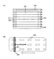
以下、本発明のレーザー照射装置の構成について図1を用いて説明する。101はレーザー発振装置である。図1では4つのレーザー発振装置を用いているが、本発明のレーザー照射装置が有するレーザー発振装置は複数であれば良く、この数に限定されない。
【0038】
レーザーは、処理の目的によって適宜変えることが可能である。本発明では、公知のレーザーを用いることができる。また、連続発振に限定されずパルス発振でも用いることができ、気体レーザーでも固体レーザーであっても良い。気体レーザーとして、エキシマレーザー、Arレーザー、Krレーザーなどがあり、固体レーザーとして、YAGレーザー、YVO4レーザー、YLFレーザー、YAlO3レーザー、ガラスレーザー、ルビーレーザー、アレキサンドライドレーザー、Ti:サファイアレーザー、Y2O3レーザーなどが挙げられる。固体レーザーとしては、Cr、Nd、Er、Ho、Ce、Co、Ti、Yb又はTmがドーピングされたYAG、YVO4、YLF、YAlO3などの結晶を使ったレーザーが適用される。当該レーザーの基本波はドーピングする材料によって異なり、1μm前後の基本波を有するレーザー光が得られる。基本波に対する高調波は、非線形光学素子を用いることで得ることができる。
【0039】
またさらに、固体レーザーから発せられらた赤外レーザー光を非線形光学素子でグリーンレーザー光に変換後、さらに別の非線形光学素子によって得られる紫外レーザー光を用いることもできる。
【0040】
なお、レーザー発振装置101は、チラー102を用いてその温度を一定に保つようにしても良い。チラー102は必ずしも設ける必要はないが、レーザー発振装置101の温度を一定に保つことで、出力されるレーザー光のエネルギーが温度によってばらつくのを抑えることができる。
【0041】
また104は光学系であり、レーザー発振装置101から出力された光路を変更したり、そのレーザー光の照射領域の形状を加工したりして、レーザー光を集光することができる。さらに、本発明の光学系104で重要なのは、複数のレーザー発振装置101から出力されたレーザー光を互いに一部を重ね合わせて合成することができることである。レーザー光を重ね合わせるとは、レーザー光の照射領域を重ね合わせることを意味する。
【0042】
なお、レーザー光の進行方向を高速で変えることができるAO変調器103を、被処理物である基板106とレーザー発振装置101との間の光路に設けて、シャッターとして使用しても良い。
【0043】
合成されたレーザー光は、スリット105を介して被処理物である基板106に照射される。スリット105は、レーザー光を部分的に遮ることが可能であり、なおかつレーザー光によって変形または損傷しないような材質で形成するのが望ましい。スリット105はレーザー光を通す開口部の幅(以下、スリットの幅と呼ぶ)が可変であっても良く、該スリットの幅によってレーザー光の走査方向の幅を制御することができる。
【0044】
なお、スリット105を介さない場合の、レーザー発振装置101から発振されるレーザー光の基板106におけるレーザー光の照射領域の形状は、レーザーの種類によって異なり、また光学系により成形することもできる。
【0045】
基板106はステージ107上に載置されている。図1では、位置制御手段108、109が、被処理物におけるレーザー光の照射位置を制御する手段に相当し、ステージ107の位置が、位置制御手段108、109によって制御されている。図1では位置制御手段108、109を用いて基板の位置を変えることで、レーザー光を基板上において相対的に移動(走査)させたり、レーザー光の走査方向を変えたりすることができる。位置制御手段108がX方向におけるステージ107の位置の制御を行っており、位置制御手段109はY方向におけるステージ107の位置制御を行う。
【0046】
また本発明のレーザー照射装置は、中央演算処理装置及びメモリ等の記憶手段を兼ね備えたコンピューター110を有していても良い。コンピューター110は、レーザー発振装置101の発振を制御し、なおかつ位置制御手段108、109を制御し、基板を所定の位置に定めることができる。コンピューター110によって、該スリット105の幅を制御するようにしても良い。
【0047】
さらに本発明のレーザー照射装置は、被処理物の温度を調節する手段を備えていても良い。また、レーザー光は指向性およびエネルギー密度の高い光であるため、ダンパーを設けて、反射光が不適切な箇所に照射されるのを防ぐようにしても良い。ダンパーは、反射光を吸収させる性質を有していることが望ましく、ダンパー内に冷却水を循環させておき、反射光の吸収により隔壁の温度が上昇するのを防ぐようにしても良い。また、ステージ107に基板を加熱するための手段(基板加熱手段)を設けるようにしても良い。
【0048】
また基板106の位置合わせのために、CCDカメラ113を1台、場合によっては数台設けるようにしても良い。
【0049】
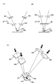
次に、複数のレーザー光を重ね合わせることで合成される、レーザー光の照射領域の形状について説明する。
【0050】
図2(A)に、合成前のレーザー光の照射領域の形状の一例を示す。図2(A)に示したレーザー光は楕円形状を有している。なお本発明のレーザー照射装置において、レーザー光の照射領域の形状は、楕円に限定されない。レーザー光の照射領域の形状はレーザーの種類によって異なり、また光学系により成形することもできる。例えば、ラムダ社製のXeClエキシマレーザー(波長308nm、パルス幅30ns)L3308から射出されたレーザー光の照射領域の形状は、10mm×30mm(共にビームプロファイルにおける半値幅)の矩形状である。また、YAGレーザーから射出されたレーザー光の照射領域の形状は、ロッド形状が円筒形であれば円状となり、スラブ型であれば矩形状となる。このようなレーザー光を光学系により、さらに成形することにより、所望の大きさのレーザー光をつくることもできる。
【0051】
図2(B)に図2(A)に示したレーザー光の長軸L方向におけるレーザー光のエネルギー密度の分布を示す。レーザー光が楕円形状であるレーザー光のエネルギー密度の分布は、楕円の中心Oに向かうほど高くなっている。
【0052】
次に、レーザー光を合成したときの、レーザー光の照射領域の形状を、図2(C)に示す。なお図3(A)では4つのレーザー光の照射領域を重ね合わせることで1つのレーザー光を形成した場合について示しているが、重ね合わせるレーザー光の数はこれに限定されない。
【0053】
図2(C)に示すように、各レーザー光の照射領域は、各楕円の長軸が一致し、なおかつ互いにレーザー光の一部が重なることで合成され、1つのレーザー光を形成している。なお以下、各楕円の中心Oを結ぶことで得られる直線を中心軸と呼ぶ。
【0054】
図2(D)に、図2(C)に示した合成後のレーザー光の、中心軸方向におけるレーザー光のエネルギー密度の分布を示す。合成前の各レーザー光が重なり合っている部分において、エネルギー密度が加算される。例えば図示したように重なり合ったビームのエネルギー密度AとBを加算すると、ビームのエネルギー密度のピーク値Cとほぼ等しくなり、各楕円の中心Oの間においてエネルギー密度が平坦化される。
【0055】
なお、AとBを加算するとCと等しくなるのが理想的だが、現実的には必ずしも等しい値にはならない。AとBを加算した値とCとの値のずれは、Cの値の±10%、より望ましくは±5%以内であると良いが、許容範囲は設計者が適宜設定することが可能である。
【0056】
図2(D)からわかるように、複数のレーザー光を重ね合わせてエネルギー密度の低い部分を互いに補い合うようにすることで、複数のレーザー光を重ね合わせないで単独で用いるよりも、半導体膜の結晶性を効率良く高めることができる。例えば図2(A)の斜線で示した領域においてのみ、所望の結晶を得るために必要なエネルギー密度を満たしており、その他の領域ではエネルギー密度が所望の値まで満たされていなかったと仮定する。この場合、各レーザー光は、中心軸方向の幅がαで示される斜線の領域でしか、所望の結晶を得ることができない。しかし、レーザー光を図2(D)で示したように重ね合わせることで、中心軸方向の幅がβ(β>4α)で示される領域において所望の結晶を得ることができ、より効率良く半導体膜を結晶化させることができる。
【0057】
さらに本発明では、レーザー光の中心軸に対し垂直な方向において、エネルギー密度が所望の値まで達していない領域を、スリット105によって遮蔽する。図3を用いて、合成されたレーザー光とスリットとの位置関係について説明する。
【0058】
本発明で用いられるスリット105は、スリットの幅を可変とし、さらにその幅をコンピューター110によって制御するようにしても良い。図3(A)において、120は図2(C)に示した合成により得られるレーザー光の照射領域の形状を示している。またレーザー光120のうち、エネルギー密度が所定の値を超えている領域を120aで示し、所定の値以下の領域を120bで示した。105はスリットを示しており、図3(A)では、レーザー光120がスリットによって遮蔽されていない様子を示している。
【0059】
図3(B)に、スリット105によって一部が遮蔽されたレーザー光の様子を示す。図3(B)に示すように本発明では、レーザー光120の中心軸の垂直方向において、領域120aを挟んで存在する領域120bを、スリット105によって遮蔽する。そして図3(C)は図3(B)に示したレーザー光の中心軸に垂直なA−A’におけるエネルギー密度の分布を示しており、少なくともエネルギー密度が所定の値(例えばT)以下の領域が、スリット105によって遮蔽されているのがわかる。
【0060】
上記構成により、中心軸の垂直方向におけるレーザー光のエネルギー密度の平均値を高めることができ、面積あたりのレーザー光の照射時間を抑え、なおかつ被処理物に与えるトータルの熱量を高めることができる。よって、基板が加熱されるのを抑えつつ、半導体膜の結晶性を高めることができる。
【0061】
なお、本発明ではさらに、レーザー光の中心軸方向において、領域120aを挟んで存在する領域120bを、スリット105によって遮蔽するようにしても良い。図4(A)に、スリット105によってレーザー光の中心軸方向において、領域120aを挟んで存在する領域120bを遮蔽した様子を示す。さらに、図4(B)に、図4(A)に示したレーザー光の、中心軸方向におけるエネルギー密度の分布を示す。図4(B)に示すように、少なくともエネルギー密度が所定の値(例えばT)以下の領域が、スリット105によって遮蔽されているのがわかる。
【0062】
エネルギー密度の低い領域により結晶化された半導体膜は、結晶性が芳しくない。具体的には、所定のエネルギー密度が得られている領域と比べて、結晶粒が小さかったり、結晶粒の成長する方向が異なっていたりする。よってエネルギー密度の低い領域が、後に形成される活性層と重ならないように、レーザー光の走査経路及び活性層のレイアウトを決める必要がある。図4(B)に示したエネルギー密度の分布を有するレーザー光を用いることで、エネルギー密度の低い領域が存在しなくなる、または狭くなるので、レーザー光の走査経路及び活性層のレイアウトにおける制約を小さくすることができる。
【0063】
さらに本発明では、図1のコンピューター110において、マスクのパターン情報に従い、レーザー光を走査する部分を定めるようにしても良い。この場合、コンピューター110では、定められた走査する部分にレーザー光があたるように、位置制御手段108、109を制御して、半導体膜を部分的に結晶化する。これにより必要不可欠な部分を最低限結晶化できるようにレーザー光を走査することができるので、基板全面にレーザー光を照射する必要がなくなり、基板の処理効率を高めることができる。
【0064】
次に、図3(B)に示した形状の照射領域を有するレーザー光を用いた、半導体装置の作製方法について説明する。
【0065】
まず、図5(A)に示すように、矩形またはストライプ形状の凸部201aを有する下地膜201を基板上に形成する。図5(A)のA−A’における断面図が図5(B)に相当する。
【0066】
基板(図示せず)は、後の工程の処理温度に耐えうる材質であれば良く、例えば石英基板、シリコン基板、バリウムホウケイ酸ガラスまたはアルミノホウケイ酸ガラスなどのガラス基板、金属基板またはステンレス基板の表面に絶縁膜を形成した基板を用いることができる。また、処理温度に耐えうる程度に耐熱性を有するプラスチック基板を用いてもよい。
【0067】
また本実施の形態では、下地膜201として酸化珪素膜を用いた。なお、下地膜201の材料はこれに限定されず、後の工程における熱処理に耐え得る材料で、なおかつTFTの特性に悪影響を与えうるアルカリ金属が、後に形成される半導体膜に混入するのを防ぐことができ、凹凸を形成することができる絶縁膜であれば良い。なおこの凹凸の形成の仕方については、後段において詳しく説明する。また、これらの他の絶縁膜を用いても良いし、単一の層からなる絶縁膜ではなく2層以上の絶縁膜の積層構造であってもよい。
【0068】
次に、下地膜201を覆うように半導体膜202を形成する。半導体膜202は、公知の手段(スパッタ法、LPCVD法、プラズマCVD法等)により成膜することができる。なお、半導体膜は非晶質半導体膜であっても良いし、微結晶半導体膜、結晶質半導体膜であっても良い。また珪素だけではなくシリコンゲルマニウムを用いるようにしても良い。シリコンゲルマニウムを用いる場合、ゲルマニウムの濃度は0.01〜4.5atomic%程度であることが好ましい。また、下地膜201を成膜した後、大気開放せずに連続的に成膜することで、半導体膜と下地膜との間に不純物が混入するのを防ぐことができる。
【0069】
なお、凸部間の幅が広すぎたり狭すぎたりすると、凹部近傍において凸部上よりも半導体膜の結晶性が優れているという本発明の効果が著しく小さくなる。また凸部の高さが高すぎると、後に形成される配線が凸部のエッジ近傍において段切れを起こす可能性が高くなる。また、低すぎると、凹部近傍において凸部上よりも半導体膜の結晶性が優れているという本発明の効果が著しく小さくなる。
【0070】
凸部201aの断面形状及びそのサイズついては、半導体膜の厚さとの兼ね合いを考慮し、設計者が適宜設定することができる。凸部間の幅Wsは0.01μm〜2μm、より望ましくは0.1μm〜1μm程度にするのが好ましい。また、凸部の高さWhは0.01μm〜3μm、より望ましくは0.1μm〜2μm程度にするのが好ましい。または凸部の高さを小さくし、Whを0.01μm〜1μm、より望ましくは0.05μm〜0.2μm程度にしても良い。
【0071】
次に、図5(C)に示すように、半導体膜202に図3(B)に示したレーザー光を照射する。なお、図5(D)は、図5(C)の破線A−A’における断面図に相当する。
【0072】
本実施の形態では、図5(C)において矢印で示したように、走査方向を矩形の凸部201aの長手方向に揃えてレーザー光を照射したが、本発明はこの構成に限定されない。レーザー光の走査方向は設計者が適宜設定することが可能である。レーザー光の照射により、半導体膜202は一次的に溶融し、図5(D)において白抜きの矢印で示したように、凸部の上部から凹部に向かってその体積が移動する。そして表面が平坦化され、なおかつ結晶性が高められた半導体膜203が形成される。レーザー光のエネルギー密度は、レーザービームのエッジの近傍において低くなっており、そのためエッジの近傍は結晶粒が小さく、結晶の粒界に沿って突起した部分(リッジ)が出現する。そのため、レーザー光のレーザービームの軌跡のエッジと、チャネル形成領域となる部分または半導体膜202の凹部上に位置する部分とが重ならないように照射する。
【0073】
半導体膜203は、レーザー光の照射による体積移動により、下地膜201の凹部上において膜厚が厚くなり、逆に凸部201a上において膜厚が薄くなる。そのため応力によって凸部上に粒界204が発生しやすく、逆に凹部上においては結晶性の良い状態が得られる。なお、凹部上において半導体膜203が必ずしも粒界を含まないわけではない。しかし、たとえ粒界が存在したとしても結晶粒が大きいので、結晶性は比較的優れたものとなっている。
【0074】
なお、半導体膜の結晶化に際し、レーザー光の照射の工程と、触媒を用いて半導体膜を結晶化させる工程とを組み合わせていても良い。触媒元素を用いる場合、特開平7−130652号公報、特開平8−78329号公報で開示された技術を用いることができる。
【0075】
次に、図6(A)に示すように、半導体膜203の表面をエッチングしていき、下地膜201の凸部201aの上面を露出させる。なお、図6(B)は、図6(A)の破線A−A’における断面図に相当する。上記工程により、下地膜201の凹部に存在する半導体膜205が形成される。半導体膜203の上面からの除去は、どのような方法を用いて行っても良く、例えばエッチングにより行っても良いし、CMP法により行っても良い。
【0076】
この上面からの除去により、凸部201a上の粒界が存在する部分が除去され、凸部201a間に相当する凹部の上には、後にチャネル形成領域となる結晶性の良い半導体膜が残される。
【0077】
次に、図6(C)に示すように半導体膜205をパターニングすることで、活性層となる島状の半導体膜206を形成する。なお、図6(D)は、図6(C)の破線A−A’における断面図に相当する。島状の半導体膜206は、凸部201a間に形成される凹部上にその一部が存在する。さらに、半導体膜206は、その一部が凸部201aと接している。TFTのチャネル形成領域は、半導体膜205の凹部上に位置する部分を用いて形成されるように、そのチャネル長、チャネル幅を考慮して、凸部201aのレイアウトを定めるのが望ましい。なお、ソース領域またはドレイン領域となる部分をも凹部上に存在する半導体膜で形成することで、ソース領域とドレイン領域の抵抗を下げることができる。
【0078】
なお、図6では各島状の半導体膜206が、凸部201aと重なっていないが、本発明はこの構成に限定されない。島状の半導体膜206の一部が凸部201a上に重なっていても良い。さらに、互いに分離した複数のチャネル形成領域と、全ての複数のチャネル形成領域を間に挟んでいるソース領域及びドレイン領域とを有し、全ての複数のチャネル形成領域が凸部201aと重なっておらず、ソース領域及びドレイン領域は凸部と一部重なっている、所謂マルチチャネル型のTFTであっても良い。
【0079】
また、図6では凸部201aが残ったままであるが、島状の半導体膜206を形成した後、凸部201aを除去しても良い。図7(A)に凸部201aを除去した後の島状の半導体膜206の様子を示す。また図7(A)のA−A’における断面図を図7(B)に示す。
【0080】
上述した図6までの、一連の工程によって得られた島状の半導体膜を、活性層として用い、TFTを作製する。互いに分離した複数のチャネル形成領域を有するTFTの作製工程及びその具体的な構造は様々である。代表的には、島状の半導体膜に不純物を添加し、ソース領域とドレイン領域を形成する工程と、ゲート絶縁膜を形成する工程と、ゲート電極を形成する工程とが行われる。
【0081】
なお、本実施の形態ではレーザー光で結晶化した半導体膜の表面を、凸部が露出する程度に除去する工程の後に、パターニングにより島状の半導体膜を形成する工程を行なっているが、本発明はこの構成に限定されない。パターニングにより島状の半導体膜を形成する工程の後に、凸部が露出する程度に島状の半導体膜の表面を除去する工程を行なっても良い。また、半導体膜をパターニングしてからレーザーで結晶化するようにしても良い。
【0082】
本発明では、絶縁膜の凹部上に位置する半導体膜を、TFTの活性層として積極的に用いることで、TFTのチャネル形成領域に粒界が形成されるのを防ぐことができ、粒界によってTFTの移動度が著しく低下したり、オン電流が低減したり、オフ電流が増加したりするのを防ぐことができ、TFTの特性のバラツキを抑えることができる。
【0083】
そして、TFTを作製した後、目的とする半導体装置の仕様に合わせて、各TFTのゲート電極、ソース領域、ドレイン領域を電気的に接続する配線を形成する。結晶化後の半導体膜をTFTの活性層として用いる場合、レーザー光の走査方向は、チャネル形成領域のキャリアが移動する方向と平行になるように定めるのが望ましい。図8に、上記TFTを用いてインバーターとトランスミッションゲートを作製した例について説明する。
【0084】
図8(A)に、本発明の作製方法を用いて形成されたインバーターとトランスミッションゲートの上面図を、図8(B)にその回路図を示す。上述した一連の作製方法を用いて形成された島状の半導体膜を用いて、pチャネル型TFT210、211、nチャネル型TFT212、213を形成する。これらのTFT210〜213は、少なくとも活性層と、ゲート絶縁膜と、ゲート電極とをそれぞれ有している。そして各活性層にはチャネル形成領域と、該チャネル形成領域を挟んでいるソース領域とドレイン領域とが少なくとも設けられている。
【0085】
なお、ソース領域またはドレイン領域となる不純物領域と、チャネル形成領域との間にLDD領域やオフセット領域を有していてもよい。
【0086】
各TFTは凹部上に活性層を有しており、各活性層は凸部201a間に位置し、かつ凸部201aとは重なっていない。そして、配線215〜220によって、各TFTのソース領域、ドレイン領域またはゲート電極が接続されることで、図8(B)に示した回路図を有する回路を形成することができる。具体的には、pチャネル型TFT210とnチャネル型TFT212とでインバーターを形成されている。また、pチャネル型TFT211とnチャネル型TFT213とでトランスミッションゲートが形成されている。Aに入力された信号に同期して、Inから入力された信号がサンプリングされOutから出力される。
【0087】
なお、本発明の作製方法を用いて作製される半導体装置は、上記回路に限定されないことは言うまでもない。また、図8(A)では、配線215〜220が同じ層に形成されているが、本発明はこれに限定されない。各TFTを接続する配線は、異なる層に形成されていても良い。各配線を異なる層に形成することで、複雑な接続が可能になり、同じ数のTFTから形成することができる回路の種類が豊富になる。なおTFTの接続は、ダマシンプロセス等によって作製された配線(プラグ)によって行なっても良い。
【0088】
なお、上記工程において、レーザー光の照射後または結晶化後の半導体膜を下地膜の凸部が露出する程度にエッチングした後において、500〜600℃で1分から60分程度加熱することで、半導体膜内において生じている応力を緩和することができる。
【0089】
本発明の作製方法を用いることで、図8(A)に示したインバーターとトランスミッションゲートの他に、例えばLSIを用いたCPU、各種ロジック回路の記憶素子(例えばSRAM)、カウンタ回路、分周回路ロジック、半導体表示装置等を形成することができる。
【0090】
図9(A)を用いて、アクティブマトリクス型の半導体装置を作製するために成膜された半導体膜230における、レーザー光の走査方向について説明する。図9(A)では、破線231が画素部、破線232が信号線駆動回路、破線233が走査線駆動回路の形成される部分に相当する。
【0091】
図9(A)では、基板が白抜きの矢印の方向に移動しており、実線の矢印はレーザー光の相対的な走査方向を示している。図9(B)は、画素部が形成される部分231におけるレーザー光の照射領域234の拡大図である。レーザー光が照射された領域に活性層235が形成される。
【0092】
なお、図9ではレーザー光の中心軸方向と走査方向とが垂直に保たれている場合について示したが、レーザー光の中心軸と走査方向とは必ずしも垂直になっていなくとも良い。例えば、レーザー光の中心軸と、走査方向との間に形成される鋭角θAが45°±35°となるようにし、より望ましくは45°となるようにしてもよい。レーザー光の中心軸と、走査する方向とが垂直の場合、最も基板の処理効率が高まる。一方合成後のレーザー光の中心軸と、走査する方向とが45°±35°となるように、望ましくは45°により近い値になるように走査することで、走査する方向とレーザー光の中心軸とが垂直になるように走査した場合に比べて、活性層中に存在する結晶粒の数を意図的に増やすことができ、結晶の方位や結晶粒に起因する特性のばらつきを低減することができる。
【0093】
【実施例】
以下、本発明の実施例について説明する。
【0094】
(実施例1)
本実施例では、絶縁膜の凹凸の長手方向に対して、レーザー光を所定の角度だけ傾けて走査させた場合について説明する。
【0095】
レーザー光は、凹凸の長手方向に沿って走査させるよりも、凹凸の長手方向に対して所定の角度だけ傾けて走査させたほうが、凹部の長手方向に対して垂直な方向における幅(以下単に、凹部の幅とする)を比較的広くしても、凹部上に粒界がさらに形成されにくくなる。この所定の角度は、45度または135度に近いことが望ましく、典型的には30度〜60度または120度〜150度程度である。
【0096】
まず、図10(A)に示すように、矩形またはストライプ形状の凸部301aを有する下地膜301を基板上に形成する。図10(A)のA−A’における断面図が図10(B)に相当する。
【0097】
本実施の形態では、下地膜301として酸化珪素膜を用いたが、下地膜301の材料はこれに限定されない。
【0098】
次に、下地膜301を覆うように、公知の手段(スパッタ法、LPCVD法、プラズマCVD法等)により半導体膜302を形成する。半導体膜302は非晶質半導体膜であっても良いし、微結晶半導体膜、結晶質半導体膜であっても良い。また珪素だけではなくシリコンゲルマニウムを用いるようにしても良い。シリコンゲルマニウムを用いる場合、ゲルマニウムの濃度は0.01〜4.5atomic%程度であることが好ましい。また、下地膜301を成膜した後、大気開放せずに連続的に成膜することで、半導体膜と下地膜との間に不純物が混入するのを防ぐことができる。
【0099】
なお、凸部間の幅が大きすぎたり小さすぎたりすると、本発明の効果は得られない。また、凸部の高さが低すぎても本発明の効果は得られない。そして、凸部の高さが高すぎると、後に形成される半導体膜が凸部のエッジ近傍において膜切れを起こすので、目的とするTFTの構造に合わせて凹凸の形状を変えることが肝要である。凸部301aの断面形状及びそのサイズついては、半導体膜の厚さとの兼ね合いを考慮し、設計者が適宜設定することができる。
【0100】
本実施の形態では、凸部間の幅(凹部の幅)Wsは、0.01μm〜3μm、より望ましくは0.1μm〜2μm程度と、レーザー光の走査方向と凹凸の長手方向とを揃えた場合よりも、Wsを比較的広くしても、本発明の効果を得ることができる。また、凸部の高さWhは0.01μm〜3μm、より望ましくは0.1μm〜2μm程度にするのが好ましい。または凸部の高さを小さくし、Whを0.01μm〜2μm、より望ましくは0.05μm〜1μm程度にしても良い。
【0101】
次に、図10(C)に示すように、半導体膜302にレーザー光を照射する。なお、図10(D)は、図10(C)の破線A−A’における断面図に相当する。
【0102】
本実施の形態では、レーザー光の走査方向は、凹凸の長手方向に対してθ=45度の角度を有している。
【0103】
レーザー光の照射により、半導体膜302は一次的に溶融し、図10(D)において白抜きの矢印で示したように、凸部の上部から凹部に向かってその体積が移動する。そして表面が平坦化され、なおかつ結晶性が高められた半導体膜303が形成される。レーザー光のエネルギー密度は、レーザービームのエッジの近傍において低くなっており、そのためエッジの近傍は結晶粒が小さく、結晶の粒界に沿って突起した部分(リッジ)が出現する。そのため、レーザー光のレーザービームの軌跡のエッジと、チャネル形成領域となる部分または半導体膜302の凹部上に位置する部分とが重ならないように照射する。
【0104】
半導体膜303は、レーザー光の照射による体積移動により、下地膜301の凹部上において膜厚が厚くなり、逆に凸部301a上において膜厚が薄くなっている。そのため応力によって凸部上に粒界104が発生しやすく、逆に凹部上においては結晶性の良い状態が得られる。なお、凹部上において半導体膜303が必ずしも粒界を含まないわけではない。しかし、たとえ粒界が存在したとしても結晶粒が大きいので、結晶性は比較的優れたものとなっている。
【0105】
半導体膜302の厚さによっては、凸部301a上の半導体膜が完全に凹部に移動してしまうことも予想される。この場合においても、凹部上の半導体膜に粒界が形成されにくいという効果に変わりはない。
【0106】
なお、半導体膜の結晶化に際し、レーザー光の照射の工程と、触媒を用いて半導体膜を結晶化させる工程とを組み合わせていても良い。触媒元素を用いる場合、特開平7−130652号公報、特開平8−78329号公報で開示された技術を用いることができる。
【0107】
そして、半導体膜303の表面をエッチングして下地膜301の凸部301aの上面を露出させ、以下実施の形態に示した場合と同様の工程を行なう。
【0108】
本実施の形態で示したように、レーザー光の走査方向を凸部の長手方向に対して所定の角度傾けると、凹部の幅を比較的広くしても、凹部上に粒界が形成されにくくなる。どこまで凹部の幅を広げても、粒界が形成されにくいという効果が得られるのかは、レーザー光の走査速度、エネルギー密度、半導体膜の厚さ、凹部の厚さ等の諸条件にある程度左右される。しかし、レーザー光の走査方向を凸部の長手方向に一致させた場合よりも、凹部の幅の許容範囲は広い。
【0109】
そして凹部の幅が1.5μm以上でも本発明の効果を十分得ることができるため、最小加工寸法が1.5μm以上の露光装置を用いることが可能になる。ステッパと呼ばれる縮小投影露光装置は解像度が優れており、1μm以下のパターンを転写するのに適しているが、22mm角程度づつステップしながら露光するため、露光時間が比較的長いという欠点がある。また、ガラス基板表面の数μm程度の凹凸によりパターンがずれてしまいやすい。一方、等倍投影露光の場合、縮小投影露光に比べて解像度が劣っており、1.5μm以上のパターンしか対応できない。しかし、ガラス基板表面の数μm程度のうねりではパターンのずれは起きにくく、また露光面積が50mm角〜100mm角程度と、一般的にステッパに比べて広いため、露光時間が短縮できる。本実施の形態では、凹凸を形成するためのパターンが、1.5μm以上の最小加工寸法で十分であるので、等倍投影露光法を用いた露光装置でも十分対応可能である。
【0110】
(実施例2)
本実施例では、凹凸を有する下地膜の形成の仕方について説明する。なお本実施例で示す下地膜はほんの一例であり、本発明で用いられる下地膜は、本実施例で示す構成に限定されない。
【0111】
まず、図11(A)に示すように、基板250上に絶縁膜からなる第1の下地膜251を成膜する。第1の下地膜251は本実施例では酸化窒化珪素を用いるがこれに限定されず、第2の下地膜とエッチングにおける選択比が大きい絶縁膜であれば良い。本実施例では第1の下地膜251をCVD装置でSiH4とN2Oを用いて50〜200nmの厚さになるように形成した。なお第1の下地膜は単層であっても、複数の絶縁膜を積層した構造であってもよい。
【0112】
次に、図11(B)に示すように、第1の下地膜251に接するように絶縁膜からなる第2の下地膜252を形成する。第2の下地膜252は後の工程においてパターニングし、凹凸を形成したときに、その後に成膜される半導体膜の表面に凹凸が現れる程度の膜厚にする必要がある。本実施例では第2の下地膜252として、プラズマCVD法を用いて30nm〜300nmの酸化珪素を形成する。
【0113】
次に、図11(C)に示すようにマスク253を形成し、第2の下地膜252をエッチングする。なお本実施例では、フッ化水素アンモニウム(NH4HF2)を7.13%とフッ化アンモニウム(NH4F)を15.4%含む混合溶液(ステラケミファ社製、商品名LAL500)をエッチャントとし、20℃においてウエットエッチングを行う。このエッチングにより、矩形状の凸部254が形成される。本明細書では、第1の下地膜251と凸部253とを合わせて1つの下地膜とみなす。
【0114】
なお、第1の下地膜251として窒化アルミニウム、窒化酸化アルミニウムまたは窒化珪素を用い、第2の下地膜252として酸化珪素膜を用いる場合、RFスパッタ法を用いて第2の下地膜252をパターニングすることが望ましい。第1の下地膜251として窒化アルミニウム、窒化酸化アルミニウムまたは窒化珪素は熱伝導度が高いので、発生した熱をすばやく拡散することができ、TFTの劣化を防ぐことができる。
【0115】
次に、第1の下地膜251と凸部253を覆うように半導体膜を形成する。本実施例では凸部の厚さが30nm〜300nmであるので、半導体膜の膜厚を50〜200nmとするのが望ましく、ここでは60nmとする。なお、半導体膜と下地膜との間に不純物が混入すると、半導体膜の結晶性に悪影響を与え、作製するTFTの特性バラツキやしきい値電圧の変動を増大させる可能性があるため、下地膜と半導体膜とは連続して成膜するのが望ましい。そこで本実施例では、第1の下地膜251と凸部253とからなる下地膜を形成した後は、酸化珪素膜255を薄く該下地膜上に成膜し、その後大気にさらさないように連続して半導体膜256を成膜する。酸化珪素膜の厚さは設計者が適宜設定することができるが、本実施例では5nm〜30nm程度とした。
【0116】
次に、図11とは異なる下地膜の形成の仕方について説明する。まず図12(A)に示すように基板260上に絶縁膜からなる第1の下地膜を形成する。第1の下地膜は、酸化珪素膜、窒化珪素膜、酸化窒化珪素膜などで形成する。
【0117】
酸化珪素膜を用いる場合には、プラズマCVD法で、オルトケイ酸テトラエチル(Tetraethyl Orthosilicate:TEOS)とO2とを混合し、反応圧力40Pa、基板温度300〜400℃とし、高周波(13.56MHz)電力密度0.5〜0.8W/cm2で放電させて形成することができる。酸化窒化珪素膜を用いる場合には、プラズマCVD法でSiH4、N2O、NH3から作製される酸化窒化珪素膜、またはSiH4、N2Oから作製される酸化窒化珪素膜で形成すれば良い。この場合の作製条件は反応圧力20〜200Pa、基板温度300〜400℃とし、高周波(60MHz)電力密度0.1〜1.0W/cm2で形成することができる。また、SiH4、N2O、H2から作製される酸化窒化水素化珪素膜を適用しても良い。窒化珪素膜も同様にプラズマCVD法でSiH4、NH3から作製することが可能である。
【0118】
第1の下地膜は20〜200nm(好ましくは30〜60nm)の厚さに基板の全面に形成した後、図12(B)に示すように、フォトリソグラフィーの技術を用いマスク262を形成する。そして、エッチングにより不要な部分を除去して、矩形状の凸部263を形成する。第1の下地膜261に対してはフッ素系のガスを用いたドライエッチング法を用いても良いし、フッ素系の水溶液を用いたウエットエッチング法を用いても良い。後者の方法を選択する場合には、例えば、フッ化水素アンモニウム(NH4HF2)を7.13%とフッ化アンモニウム(NH4F)を15.4%含む混合溶液(ステラケミファ社製、商品名LAL500)でエッチングすると良い。
【0119】
次いで、凸部263及び基板260を覆うように、絶縁膜からなる第2の下地膜264を形成する。この層は第1の下地膜261と同様に酸化珪素膜、窒化珪素膜、酸化窒化珪素膜などで50〜300nm(好ましくは100〜200nm)の厚さに形成する。
【0120】
上記作製工程によって、凸部263及び第2の下地膜264からなる下地膜が形成される。なお、第2の下地膜264を形成した後、大気に曝さないように連続して半導体膜を成膜するようにすることで、半導体膜と下地膜の間に大気中の不純物が混入するのを防ぐことができる。
【0121】
本実施例は実施例1と自由に組み合わせて実施することが可能である。
【0122】
(実施例3)
本実施例では、レーザー光を重ね合わせるための光学系について説明する。
【0123】
図13に、本実施例の光学系の具体的な構成を示す。図13(A)は本発明のレーザー照射装置の光学系の側面図であり、図13(A)の矢印Bの方向から見た側面図を図13(B)に示す。なお図13(B)の矢印Aの方向から見た側面図が、図13(A)に相当する。図13(C)は、図13(A)、図13(B)に示した光学系の斜視図に相当する。
【0124】
図13では、レーザー光を4つ合成して1つのレーザー光にする場合の光学系を示している。なお本実施例において合成するレーザー光の数はこれに限定されず、合成するレーザー光の数は2以上8以下であれば良い。
【0125】
本実施例の光学系は、6つのシリンドリカルレンズ401、402、403、404、405、406を用いている。シリンドリカルレンズ403、404、405、406のそれぞれに、異なるレーザー発振装置からレーザー光が入射する。
【0126】
そしてシリンドリカルレンズ403、405によってそのレーザー光の照射領域の形状が加工されたレーザー光が、シリンドリカルレンズ401に入射する。入射したレーザー光はシリンドリカルレンズにおいてそのレーザー光の照射領域の形状が加工された後、スリット410において一部がカットされて、被処理物400に照射される。また、シリンドリカルレンズ404、406によってそのレーザー光の照射領域の形状が加工されたレーザー光が、シリンドリカルレンズ402に入射する。入射したレーザー光はシリンドリカルレンズにおいてそのレーザー光の照射領域の形状が加工された後、スリット410において一部がカットされて、被処理物400に照射される。
【0127】
被処理物400におけるレーザー光の照射領域は互いに一部重なることで合成されて、1つのレーザー光になっている。
【0128】
なお、本実施例では、被処理物400に最も近いシリンドリカルレンズ401、402の焦点距離を20mmとし、シリンドリカルレンズ403〜406の焦点距離を150mmとする。そしてシリンドリカルレンズ401、402から被処理物400へのレーザー光の入射角θ1は、本実施例では25°とし、シリンドリカルレンズ403〜406からシリンドリカルレンズ401、402へのレーザー光の入射角θ2を10°とするように各レンズを設置する。
【0129】
なお各レンズの焦点距離及び入射角は設計者が適宜設定することが可能である。さらに、シリンドリカルレンズの数もこれに限定されず、また用いる光学系はシリンドリカルレンズに限定されない。本発明は、各レーザー発振装置から発振されるレーザー光の照射領域を、半導体膜の結晶化に適した形状及びエネルギー密度になるように加工し、なおかつ全てのレーザー光の照射領域を互いに重ね合わせて合成し、1つのレーザー光にすることができるような光学系であれば良い。
【0130】
なお本実施例では、4つのレーザー光を合成する例について示しており、この場合4つのレーザー発振装置にそれぞれ対応するシリンドリカルレンズを4つと、該4つのシリンドリカルレンズに対応する2つのシリンドリカルレンズとを有している。n(n=2、4、6、8)のレーザー光を合成する場合、nのレーザー発振装置にそれぞれ対応するnのシリンドリカルレンズと、該nのシリンドリカルレンズに対応するn/2のシリンドリカルレンズとを有している。n(n=3、5、7)のレーザー光を合成する場合、nのレーザー発振装置にそれぞれ対応するnのシリンドリカルレンズと、該nのシリンドリカルレンズに対応する(n+1)/2のシリンドリカルレンズとを有している。
【0131】
次に、8つのレーザー発振装置を用いた本発明のレーザー照射装置の、光学系について説明する。
【0132】
図14(A)、図14(B)に、本実施例のレーザー照射装置に用いられる光学系の具体的な構成を示す。図14(A)は本発明のレーザー照射装置の光学系の側面図であり、図14(A)の矢印Bの方向から見た側面図を図14(B)に示す。なお図14(B)の矢印Aの方向から見た側面図が、図14(A)に相当する。図14(C)は、図14(A)、図14(B)に示した光学系の斜視図に相当する。
【0133】
図14ではレーザー光を8つ合成して1つのレーザー光にする場合の光学系を示している。なお本実施例において合成するレーザー光の数はこれに限定されず、合成するレーザー光の数は2以上8以下であれば良い。
【0134】
本実施例の光学系は、12のシリンドリカルレンズ441〜452を用いている。シリンドリカルレンズ441〜444のそれぞれに、異なるレーザー発振装置からレーザー光が入射される。
【0135】
そしてシリンドリカルレンズ450、445によってそのレーザー光の照射領域の形状が加工されたレーザー光が、シリンドリカルレンズ441に入射する。入射したレーザー光はシリンドリカルレンズ441においてそのレーザー光の照射領域の形状が加工された後、スリット460において一部がカットされて、被処理物440に照射される。また、シリンドリカルレンズ451、446によってそのレーザー光の照射領域の形状が加工されたレーザー光が、シリンドリカルレンズ442に入射する。入射したレーザー光はシリンドリカルレンズ442においてそのレーザー光の照射領域の形状が加工された後、スリット460において一部がカットされて、被処理物440に照射される。また、シリンドリカルレンズ449、447によってそのレーザー光の照射領域の形状が加工されたレーザー光が、シリンドリカルレンズ443に入射する。入射したレーザー光はシリンドリカルレンズ443においてそのレーザー光の照射領域の形状が加工された後、スリット461において一部がカットされて、被処理物440に照射される。また、シリンドリカルレンズ452、448によってそのレーザー光の照射領域の形状が加工されたレーザー光が、シリンドリカルレンズ444に入射する。入射したレーザー光はシリンドリカルレンズ444においてそのレーザー光の照射領域の形状が加工された後、スリット461において一部がカットされて、被処理物440に照射される。
【0136】
被処理物440におけるレーザー光の照射領域は互いに一部重なることで合成されて、1つのレーザー光になっている。
【0137】
なお、本実施例では、被処理物440に最も近いシリンドリカルレンズ441〜444の焦点距離を20mmとし、シリンドリカルレンズ445〜452の焦点距離を150mmとする。そしてシリンドリカルレンズ441〜444から被処理物440へのレーザー光の入射角θ1は、本実施例では25°とし、シリンドリカルレンズ445〜452からシリンドリカルレンズ441〜444へのレーザー光の入射角θ2を10°とするように各レンズを設置する。
【0138】
なお各レンズの焦点距離及び入射角は設計者が適宜設定することが可能である。さらに、シリンドリカルレンズの数もこれに限定されず、また用いる光学系はシリンドリカルレンズに限定されない。本発明は、各レーザー発振装置から発振されるレーザー光の照射領域を、半導体膜の結晶化に適した形状及びエネルギー密度になるように加工し、なおかつ全てのレーザー光の照射領域を互いに重ね合わせて合成し、1つのレーザー光にすることができるような光学系であれば良い。
【0139】
なお本実施例では、8つのレーザー光を合成する例について示しており、この場合8つのレーザー発振装置にそれぞれ対応するシリンドリカルレンズを8つと、該8つのシリンドリカルレンズに対応する4つのシリンドリカルレンズとを有している。
【0140】
レーザー光を5つ以上重ね合わせるとき、光学系を配置する場所及び干渉等を考慮すると、5つ目以降のレーザー光は基板の反対側から照射するのが望ましく、この場合基板は透過性を有していることが必要である。
【0141】
また、均一なレーザー光の照射を実現するためには、照射面に垂直な平面であって、かつ合成前の各ビームの形状をそれぞれ長方形と見立てたときの短辺を含む面または長辺を含む面のいずれか一方を入射面と定義すると、前記レーザー光の入射角度θは、入射面に含まれる前記短辺または前記長辺の長さがW、前記照射面に設置され、かつ、前記レーザー光に対して透光性を有する基板の厚さがdであるとき、θ≧arctan(W/2d)を満たすのが望ましい。この議論は合成前の個々のレーザー光について成り立つ必要がある。なお、レーザー光の軌跡が、前記入射面上にないときは、該軌跡を該入射面に射影したものの入射角度をθとする。この入射角度θでレーザー光が入射されれば、基板の表面での反射光と、前記基板の裏面からの反射光とが干渉せず、一様なレーザー光の照射を行うことができる。以上の議論は、基板の屈折率を1として考えた。実際は、基板の屈折率が1.5前後のものが多く、この数値を考慮に入れると上記議論で算出した角度よりも大きな計算値が得られる。しかしながら、ビームスポットの長手方向の両端のエネルギーは減衰があるため、この部分での干渉の影響は少なく、上記の算出値で十分に干渉減衰の効果が得られる。上記のθに対する不等式は、基板がレーザビームに対して透光性のあるもの以外には適用されない。
【0142】
本実施例の構成は、実施例1または2と自由に組み合わせて実施することが可能である。
【0143】
(実施例4)
本実施例では、レーザー光を重ね合わせたときの、各レーザー光の中心間の距離と、エネルギー密度との関係について説明する。なお、説明を分かり易くするため、スリットを設けない場合について説明する。
【0144】
図15に、各レーザー光の中心軸方向におけるエネルギー密度の分布を実線で、合成されたレーザー光のエネルギー密度の分布を破線で示す。レーザー光の中心軸方向におけるエネルギー密度の値は、一般的にガウス分布に従っている。
【0145】
合成前のレーザー光において、ピーク値の1/e2以上のエネルギー密度を満たしている中心軸方向の距離を1としたときの、各ピーク間の距離をXとする。また、合成されたレーザー光において、合成後のピーク値と、バレー値の平均値に対するピーク値の割増分をYとする。シミュレーションで求めたXとYの関係を、図16に示す。なお図16では、Yを百分率で表した。
【0146】
図16において、エネルギー差Yは以下の式1の近似式で表される。
【0147】
【式1】
Y=60−293X+340X2(Xは2つの解のうち大きい方とする)
【0148】
式1に従えば、例えばエネルギー差を5%程度にしたい場合、X≒0.584となるようにすれば良いということがわかる。Y=0となるのが理想的だが、それではレーザー光の長さが短くなるので、スループットとのバランスでXを決定すると良い。
【0149】
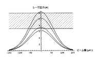
次に、Yの許容範囲について説明する。図17に、レーザー光が楕円形状を有している場合の、中心軸方向におけるビーム幅に対するYVO4レーザーの出力(W)の分布を示す。斜線で示す領域は、良好な結晶性を得るために必要な出力エネルギーの範囲であり、3.5〜6Wの範囲内に合成したレーザー光の出力エネルギーが納まっていれば良いことがわかる。
【0150】
合成後のレーザー光の出力エネルギーの最大値と最小値が、良好な結晶性を得るために必要な出力エネルギー範囲にぎりぎりに入るとき、良好な結晶性が得られるエネルギー差Yが最大になる。よって図17の場合は、エネルギー差Yが±26.3%となり、上記範囲にエネルギー差Yが納まっていれば良好な結晶性が得られることがわかる。
【0151】
なお、良好な結晶性を得るために必要な出力エネルギーの範囲は、どこまでを結晶性が良好だと判断するかによって変わり、また出力エネルギーの分布もレーザー光の照射領域の形状によって変わってくるので、エネルギー差Yの許容範囲は必ずしも上記値に限定されない。設計者が、良好な結晶性を得るために必要な出力エネルギーの範囲を適宜定め、用いるレーザーの出力エネルギーの分布からエネルギー差Yの許容範囲を設定する必要がある。
【0152】
本実施例は、実施例1〜3と組み合わせて実施することが可能である。
【0153】
(実施例5)
本実施例では、複数のレーザー光の照射領域を重ねるのではなく、複数の各レーザー光が走査された領域が互いに重なるようにレーザー光を照射する例について説明する。
【0154】
図18に、凸部501を有する絶縁膜上に形成された半導体膜502に、複数のレーザー発振装置から発せられるレーザー光を照射する様子を示す。なお図18では、凸部501の長手方向に対して45度の方向にレーザー光を走査しているが、本実施例はこの構成に限定されない。凸部501の長手方向に沿っていても良いし、長手方向に対する角度が45度以外の角度であっても良い。
【0155】
また図18では、4つのレーザー光を走査しているが、レーザー光の数はこれに限定されない。4つのレーザー光の照射領域503〜506は、それぞれ白抜きの矢印で示した方向に走査される。そして各照射領域503〜506は互いに重なってはいないが、レーザー光の走査によって各照射領域が照射される領域は、エネルギー密度の低い領域どうしが互いに重なっている。
【0156】
上記構成によって、レーザー光の照射領域を重ねなくても、半導体膜に照射されるレーザー光のエネルギー密度を均一にすることができる。よって、図2(C)に示したようにレーザー光の照射領域を重ね合わせる場合ほど光学系の精密さは要求されない。
【0157】
本実施例は、実施例1〜4と自由に組み合わせて実施することが可能である。
【0158】
【発明の効果】
本発明では、複数のレーザー発振装置から発振されたレーザー光を合成することで、各レーザー光のエネルギー密度の弱い部分を補い合うことができる。よって、複数の各レーザー発振装置から発せられるレーザー光を合成せずにそれぞれ単独で用いるよりも、レーザー光のうち、結晶化に必要な程度のエネルギー密度を有する領域が広がり、基板の処理効率を高めることができる。
【0159】
さらに本発明ではスリットを用いて、合成されたレーザー光のうち、走査方向においてエネルギー密度が所定の値以下の領域をカットする。上記構成により、走査方向におけるレーザー光のエネルギー密度の平均値を高めることができ、面積あたりのレーザー光の照射時間を抑え、なおかつ被処理物に与えるトータルの熱量を高めることができる。よって、基板が加熱されるのを抑えつつ、半導体膜の結晶性を高めることができる。
【0160】
また、絶縁膜の凹部上に位置する半導体膜を、TFTの活性層として積極的に用いることで、TFTのチャネル形成領域に粒界が形成されるのを防ぐことができ、粒界によってTFTの移動度が著しく低下したり、オン電流が低減したり、オフ電流が増加したりするのを防ぐことができる。
【0161】
また、凹部近傍の結晶性をより高めるように、凹凸を有する絶縁膜上の半導体膜を結晶化するには、レーザー光の照射により膜厚方向において完全に半導体膜を溶融させるのが望ましい。これは、凹部近傍においてレーザー光により溶融されきれなかった固相の領域が存在すると、該領域を核として成長した結晶どうしがぶつかって結晶粒が形成されてしまうためである。本発明では、走査方向においてレーザー光のエネルギー密度の低い部分をスリットで遮蔽し、照射領域内のエネルギー密度の平均値を高めることができるので、面積あたりの照射時間が同じでも、半導体膜に与えるトータルの熱量を高めることができる。よって、基板が加熱されるのを抑えつつ、半導体膜を膜厚方向において完全に溶融することができ、凹部の結晶性を高めることができる。
【図面の簡単な説明】
【図1】 本発明のレーザー照射装置の構造を示す図。
【図2】 レーザー光の照射領域の形状及びエネルギー密度の分布を示す図。
【図3】 レーザー光とスリットの位置関係を示す図。
【図4】 レーザー光とスリットの位置関係を示す図。
【図5】 本発明の半導体表示装置の作製工程を示す図。
【図6】 本発明の半導体表示装置の作製工程を示す図。
【図7】 本発明の半導体表示装置の作製工程を示す図。
【図8】 本発明の作製方法を用いて形成されたインバーター及びトランスミッションゲートの上面図及び回路図。
【図9】 被処理物においてレーザー光の移動する方向を示す図。
【図10】 本発明の半導体表示装置の作製工程を示す図。
【図11】 凸部を有する下地膜の作製方法を示す図。
【図12】 凸部を有する下地膜の作製方法を示す図。
【図13】 レーザー照射装置の光学系の図。
【図14】 レーザー照射装置の光学系の図。
【図15】 重ね合わせたレーザー光の中心軸方向におけるエネルギー密度の分布を示す図。
【図16】 レーザー光の中心間の距離とエネルギー差の関係を示す図。
【図17】 レーザー光の中心軸方向における出力エネルギーの分布を示す図。
【図18】 レーザー照射方法の一実施例を示す図。
【図19】 凸部を有する下地膜上に形成された半導体膜にレーザー光を照射して結晶化させた後の、TEMの断面像。
【図20】 凹凸を有する下地膜上に形成されたシリコンにレーザー光を照射したときの、温度分布の時間変化を示す図。
【図21】 凹凸を有する下地膜上に形成されたシリコンにレーザー光を照射したときの、温度の時間変化を示す図。[0001]
BACKGROUND OF THE INVENTION
The present invention relates to a method for manufacturing a semiconductor device in which a semiconductor film is crystallized using laser light or activated after ion implantation.
[0002]
[Prior art]
In recent years, a technology for forming a TFT on a substrate has greatly advanced, and application development to an active matrix semiconductor display device has been advanced. In particular, a TFT using a polycrystalline semiconductor film has higher field effect mobility (also referred to as mobility) than a TFT using a conventional amorphous semiconductor film, and thus can operate at high speed. For this reason, it is possible to perform control of a pixel, which has been conventionally performed by a drive circuit provided outside the substrate, with a drive circuit formed on the same substrate as the pixel.
[0003]
By the way, as a substrate used for a semiconductor device, a glass substrate is considered promising from the viewpoint of cost rather than a single crystal silicon substrate. In general, a glass substrate is inferior in heat resistance and easily deforms by heat. Therefore, when a polysilicon TFT is formed on a glass substrate, laser annealing is used to crystallize a semiconductor film in order to avoid thermal deformation of the glass substrate. Used.
[0004]
The characteristics of laser annealing are that the processing time can be significantly shortened compared to annealing methods using radiation heating or conduction heating, and the semiconductor or semiconductor film is selectively and locally heated, causing thermal damage to the substrate. It is difficult to give.
[0005]
The laser annealing method here refers to a technique for recrystallizing a damaged layer or an amorphous layer formed on a semiconductor substrate or semiconductor film, or a technique for crystallizing an amorphous semiconductor film formed on a substrate. pointing. Moreover, the technique applied to planarization and surface modification of a semiconductor substrate or a semiconductor film is also included. The laser oscillation device to be applied is a gas laser oscillation device typified by an excimer laser, or a solid-state laser oscillation device typified by a YAG laser, and a semiconductor surface layer is irradiated with laser light for several tens of nano to several tens of microseconds. It is known to be crystallized by heating for a very short time.
[0006]
[Problems to be solved by the invention]
Lasers are roughly classified into two types, pulse oscillation and continuous oscillation, depending on the oscillation method. Since the pulsed laser has a relatively high output energy, the size of the laser beam (the area where the laser beam is actually irradiated on the surface of the object to be processed) is several centimeters. 2 As described above, mass productivity can be improved. In particular, if the shape of the region irradiated with laser light is processed using an optical system to form a linear line having a length of 10 cm or more, the substrate can be efficiently irradiated with laser light, further increasing mass productivity. Can do. For this reason, it has become the mainstream to use a pulsed laser for crystallization of the semiconductor film.
[0007]
However, in recent years, it has been found that the crystal grain size formed in a semiconductor film is larger when a continuous wave laser is used than when a pulsed laser is used for crystallization of a semiconductor film. When the crystal grain size in the semiconductor film increases, the mobility of the TFT formed using the semiconductor film increases, and variations in TFT characteristics due to crystal grain interfaces (grain boundaries) are relatively suppressed. For this reason, continuous wave lasers are starting to attract attention.
[0008]
Note that a grain boundary is one of lattice defects classified as a plane defect, which is also called a crystal grain boundary. In addition to grain boundaries, surface defects include twin planes and stacking faults. In this specification, electrically active surface defects having dangling bonds, that is, grain boundaries and stacking faults are collectively referred to as grain boundaries. Collectively.
[0009]
However, a continuous wave laser generally has a smaller maximum output energy than a pulsed laser. The size of the laser beam is 10 -3 mm 2 If it is made small, the desired power necessary for crystallization of the semiconductor film can be obtained. However, since the irradiation area of the laser beam is small, the scanning time of the laser beam per substrate is long, and the substrate processing efficiency is poor.
[0010]
On the contrary, when the irradiation area of the laser beam is increased in order to increase the processing efficiency of the substrate, the energy density is naturally lowered. In order to give the semiconductor film a total amount of heat necessary for crystallization, it is necessary to lengthen the irradiation time, and the irradiation time of the laser light per area on the substrate becomes longer. Then, the substrate is heated by absorption of the laser beam, and the substrate itself is thermally deformed, or the characteristics of the TFT are easily deteriorated due to diffusion of impurities from the glass substrate to the semiconductor film. When the substrate is heated, the crystallinity of the semiconductor film is difficult to be uniform due to the heat accumulated in the substrate, and the characteristics of the TFT are likely to vary.
[0011]
In view of the above-described problems, the present invention provides a method for manufacturing a semiconductor device using a laser crystallization method that can increase the efficiency of substrate processing as compared with the related art and can suppress thermal damage to the substrate. Let it be the first problem.
[0012]
In addition, a crystalline semiconductor film manufactured using a laser annealing method is generally formed by aggregating a plurality of crystal grains. The crystal grain position and size are roughly random, although there is a difference between pulse oscillation and continuous oscillation, and it is not possible to form a crystalline semiconductor film by specifying the crystal grain position and size. difficult. Therefore, there may be a grain boundary in the active layer formed by patterning the crystalline semiconductor film into an island shape.
[0013]
Unlike crystal grains, there are innumerable recombination centers and trap centers due to amorphous structures and crystal defects at grain boundaries. It is known that when carriers are trapped in this trapping center, the grain boundary potential increases and becomes a barrier against the carriers, so that the current transport characteristics of the carriers decrease. Therefore, if there is a grain boundary in the active layer of the TFT, particularly in the channel formation region, the mobility of the TFT is significantly reduced, the on-current is reduced, and the current flows at the grain boundary, so that the off-current increases. However, it has a significant effect on the TFT characteristics. In addition, in a plurality of TFTs manufactured on the assumption that the same characteristics can be obtained, the characteristics vary depending on the presence or absence of grain boundaries in the active layer.
[0014]
The reason why the position and size of the obtained crystal grains are random when the semiconductor film is irradiated with laser light is as follows. It takes a certain amount of time for solid-phase nucleation to occur in a liquid semiconductor film completely melted by laser light irradiation. As time passes, innumerable crystal nuclei are generated in the complete melting region, and crystals grow from the crystal nuclei. Since the positions where the crystal nuclei are generated are random, the crystal nuclei are unevenly distributed. Since crystal growth ends when the crystal grains collide with each other, the position and size of the crystal grains are random.
[0015]
Therefore, it is ideal to form the channel formation region having a significant influence on the characteristics of the TFT with a single crystal grain by eliminating the influence of the grain boundary, but the amorphous silicon film having no grain boundary. It was almost impossible to form the film by laser annealing. Therefore, a TFT having an active layer made of a crystalline silicon film crystallized using a laser annealing method has not been obtained until now, which is equivalent to the characteristics of a MOS transistor manufactured on a single crystal silicon substrate.
[0016]
In view of the above-described problems, the present invention prevents the formation of grain boundaries in the channel formation region of the TFT, and the grain boundary significantly reduces the mobility of the TFT, reduces the on-current, and increases the off-current. It is an object of the present invention to provide a method for manufacturing a semiconductor device using a laser crystallization method that can prevent the above-described problem.
[0017]
[Means for Solving the Problems]
The laser irradiation apparatus according to the present invention includes a plurality of first means (laser oscillation apparatus) for oscillating laser light, and condensing the laser light oscillated from the plurality of laser oscillation apparatuses, and further, laser light on the object to be processed. A second means (optical system) for partially superimposing each other, a slit capable of shielding a part of the synthesized laser beam, and an object to be processed irradiated through the slit And a third means for controlling the irradiation position of the laser light. Furthermore, the present invention controls the oscillation of each of the plurality of first means, and the position of the laser light whose shape is controlled by the slit in the workpiece, the plurality of laser oscillation devices and the third means. You may have the 4th means controlled by synchronizing.
[0018]
By synthesizing laser beams oscillated from a plurality of laser oscillation devices, it is possible to compensate for the weak energy density of each laser beam. Therefore, rather than combining laser beams emitted from a plurality of laser oscillation devices without using them individually, a region of the laser beam having an energy density required for crystallization is widened, and the substrate processing efficiency is increased. Can be increased.
[0019]
Further, in the present invention, a region of the synthesized laser beam whose energy density is less than a predetermined height in the scanning direction is cut using a slit. With the above configuration, the average value of the energy density of laser light in the scanning direction can be increased, the irradiation time of laser light per area can be suppressed, and the total amount of heat given to the object to be processed can be increased. Therefore, the crystallinity of the semiconductor film can be improved while suppressing the substrate from being heated.
[0020]
Further, when the present applicant forms a semiconductor film over an insulating film having unevenness and irradiates the semiconductor film with a laser beam, the crystallized semiconductor film is selectively used in a portion located on the convex portion of the insulating film. It has been found that grain boundaries are formed.
[0021]
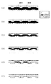
FIG. 19 shows the scanning direction of laser light when a 200 nm amorphous semiconductor film formed over an uneven insulating film is irradiated with continuous oscillation laser light at a scanning speed of 5 cm / sec. The cross-sectional image of TEM in a perpendicular direction is shown. The width of the
[0022]
FIG. 19B schematically illustrates a cross-sectional image of the TEM illustrated in FIG. As shown in FIG. 19B,
[0023]
20A to 20F show simulation results of changes over time in the temperature distribution in the semiconductor film when the semiconductor film formed over the uneven insulating film is irradiated with laser light. In the graph, the unevenness on the lower side represents the
[0024]
FIG. 20 (A) shows the temperature distribution immediately after laser light irradiation, and FIGS. 20 (B) to 20 (F) show the temperature distribution after every 2.5 μsec.
[0025]
The region where the color is dark is the portion considered to have the highest temperature, and as the state transitions from FIG. 20A to FIG. 20F, the dark portion decreases. Recognize. In particular, it can be seen that the temperature of the
[0026]
FIG. 21 shows a simulation result of temperature change with time depending on the position of the semiconductor film when the semiconductor film formed over the uneven insulating film is irradiated with laser light.
[0027]
In the graph shown in FIG. 21, the vertical axis indicates the temperature (K) of the semiconductor film, and the horizontal axis indicates time (seconds). A solid line indicates the temperature of the semiconductor film located on the convex portion, and a broken line indicates the temperature of the semiconductor film located on the concave portion. In the simulation of FIG. 21, the temperature drop due to the phase transition stops at 1600 K for the first time. However, after the phase transition, the temperature of the semiconductor film on the concave portion indicated by the broken line is higher than that of the semiconductor film on the convex portion. The descent has begun, and it can be seen that the phase transition is early.
[0028]
This is considered to be because heat is radiated more efficiently in the concave portion than in the convex portion. Therefore, after the semiconductor film is melted by laser light irradiation, in the process where the heat in the semiconductor film is dissipated and solidified by the insulating film, crystal nuclei are likely to be formed near the concave portion earlier than near the convex portion.
[0029]
As time elapses, crystal growth proceeds from the crystal nucleus generated in the vicinity of the concave portion toward the convex portion. Then, it was thought that the crystal growth proceeding from the vicinity of the adjacent concave portions collided with each other on the convex portions in the vicinity of each other may be one of the factors that caused the grain boundaries on the convex portions.
[0030]
In any case, in the semiconductor film crystallized in this way, grain boundaries are selectively formed on the convex portions, whereas grain boundaries are hardly formed on the portions located on the concave portions. In the present invention, a portion of the semiconductor film crystallized with laser light having a relatively small grain boundary provided on the recess is used for the active layer of the TFT.
[0031]
The laser light is most preferably continuous wave, but pulsed laser light may be used. Note that the cross section of the convex portion in the direction perpendicular to the scanning direction of the laser beam is preferably a quadrangle including a rectangle, or may be a triangle.
[0032]
With the above structure, grain boundaries are selectively formed on the convex portions of the semiconductor film during crystallization by laser light irradiation. The semiconductor film located on the recessed portion of the insulating film is relatively difficult to form grain boundaries. The semiconductor film located on the recessed portion of the insulating film has excellent crystallinity, but does not necessarily include the grain boundaries. However, even if a grain boundary exists, it can be said that the crystal grains are large and the crystallinity is relatively excellent as compared with the semiconductor film located on the convex portion of the insulating film. Therefore, at the stage where the shape of the insulating film is designed, the position where the grain boundary of the semiconductor film is formed can be predicted to some extent. That is, according to the present invention, the position where the grain boundary is formed can be selectively determined, so that it is possible to lay out the active layer so that the grain boundary is not included in the active layer, more preferably the channel formation region. Become.
[0033]
In the present invention, the semiconductor film located on the recess of the insulating film is positively used as the active layer of the TFT, so that it is possible to prevent the formation of a grain boundary in the TFT channel formation region. It is possible to prevent the mobility of the TFT from being significantly lowered, the on-current is reduced, and the off-current is increased.
[0034]
Note that the energy density in the vicinity of the edge of the laser beam of the laser light is generally lower than that in the vicinity of the center, and the crystallinity of the semiconductor film is often poor. For this reason, when scanning with laser light, it is desirable that the portion that will later become the channel formation region of the TFT and the edge of the locus do not overlap.
[0035]
In order to crystallize the semiconductor film on the insulating film having unevenness so that the crystallinity in the vicinity of the concave portion is further increased, it is desirable to completely melt the semiconductor film in the film thickness direction by laser light irradiation. This is because if there is a solid phase region that cannot be melted by laser light in the vicinity of the recess, crystals grown with the region as a nucleus collide with each other to form crystal grains. In the present invention, the portion where the energy density of the laser beam is low in the scanning direction can be shielded by the slit, and the average value of the energy density in the irradiation region can be increased, so even if the irradiation time per area is the same, it is given to the semiconductor film. The total amount of heat can be increased. Therefore, the semiconductor film can be completely melted in the film thickness direction while suppressing the substrate from being heated, and the crystallinity of the recess can be increased.
[0036]
Note that after the semiconductor film is formed, laser light irradiation is performed so that the semiconductor film is crystallized so that the semiconductor film is not exposed to the atmosphere (for example, a specified gas atmosphere such as a rare gas, nitrogen, oxygen, or a reduced pressure atmosphere is used). May be. With the above configuration, contaminants at the molecular level in the clean room, such as boron contained in a filter for increasing the cleanliness of air, can be prevented from being mixed into the semiconductor film during crystallization by laser light. it can.
[0037]
DETAILED DESCRIPTION OF THE INVENTION
Hereinafter, the structure of the laser irradiation apparatus of this invention is demonstrated using FIG.
[0038]
The laser can be appropriately changed depending on the purpose of processing. In the present invention, a known laser can be used. Further, it is not limited to continuous oscillation, and pulse oscillation can be used, and a gas laser or a solid laser may be used. There are excimer laser, Ar laser, Kr laser, etc. as gas laser, and YAG laser, YVO as solid laser. Four Laser, YLF laser, YAlO Three Laser, glass laser, ruby laser, alexandride laser, Ti: sapphire laser, Y 2 O Three A laser etc. are mentioned. Solid lasers include YAG, YVO doped with Cr, Nd, Er, Ho, Ce, Co, Ti, Yb or Tm. Four , YLF, YAlO Three Lasers using crystals such as are applied. The fundamental wave of the laser differs depending on the material to be doped, and a laser beam having a fundamental wave of about 1 μm can be obtained. The harmonic with respect to the fundamental wave can be obtained by using a nonlinear optical element.
[0039]
Furthermore, after converting infrared laser light emitted from a solid-state laser into green laser light by a nonlinear optical element, ultraviolet laser light obtained by another nonlinear optical element can also be used.
[0040]
Note that the
[0041]
[0042]
Note that the
[0043]
The synthesized laser light is applied to the
[0044]
Note that the shape of the laser light irradiation region on the
[0045]
The
[0046]
Further, the laser irradiation apparatus of the present invention may have a computer 110 having both a central processing unit and storage means such as a memory. The computer 110 can control the oscillation of the
[0047]
Furthermore, the laser irradiation apparatus of the present invention may include means for adjusting the temperature of the object to be processed. Further, since the laser light is light having high directivity and energy density, a damper may be provided to prevent the reflected light from being irradiated to an inappropriate place. The damper desirably has a property of absorbing reflected light, and cooling water may be circulated in the damper to prevent the temperature of the partition wall from rising due to absorption of the reflected light. Further, a means for heating the substrate (substrate heating means) may be provided on the
[0048]
In addition, one
[0049]
Next, the shape of the laser light irradiation area synthesized by superimposing a plurality of laser lights will be described.
[0050]
FIG. 2A shows an example of the shape of the laser light irradiation region before synthesis. The laser beam shown in FIG. 2A has an elliptical shape. In the laser irradiation apparatus of the present invention, the shape of the laser light irradiation region is not limited to an ellipse. The shape of the laser light irradiation area varies depending on the type of laser, and can also be formed by an optical system. For example, the shape of the irradiation region of laser light emitted from an XeCl excimer laser (wavelength 308 nm,
[0051]
FIG. 2B shows the energy density distribution of the laser light in the direction of the long axis L of the laser light shown in FIG. The distribution of the energy density of the laser beam having an elliptical laser beam becomes higher toward the center O of the ellipse.
[0052]
Next, FIG. 2C illustrates the shape of the irradiation region of the laser light when the laser light is synthesized. Note that although FIG. 3A illustrates the case where one laser beam is formed by superimposing irradiation regions of four laser beams, the number of laser beams to be superimposed is not limited thereto.
[0053]
As shown in FIG. 2C, the irradiation areas of the respective laser beams are synthesized by the long axes of the respective ellipses being coincident with each other and a part of the laser beams overlapping each other to form one laser beam. . Hereinafter, a straight line obtained by connecting the centers O of the ellipses is referred to as a central axis.
[0054]
FIG. 2D shows the energy density distribution of the laser light in the central axis direction of the combined laser light shown in FIG. The energy density is added at the portion where the laser beams before synthesis overlap. For example, when the energy densities A and B of the overlapping beams are added as shown in the figure, the peak value C of the energy density of the beams is approximately equal, and the energy density is flattened between the centers O of the ellipses.
[0055]
Note that when A and B are added, it is ideally equal to C, but in reality, it is not necessarily equal. The deviation between the value obtained by adding A and B and the value of C should be within ± 10%, more preferably within ± 5% of the value of C, but the allowable range can be set appropriately by the designer. is there.
[0056]
As can be seen from FIG. 2D, by superimposing a plurality of laser beams and complementing each other with a low energy density, the semiconductor film can be formed more than using a plurality of laser beams without overlapping. Crystallinity can be increased efficiently. For example, it is assumed that the energy density necessary for obtaining the desired crystal is satisfied only in the region indicated by the oblique lines in FIG. 2A, and the energy density is not satisfied to the desired value in the other regions. In this case, each laser beam can obtain a desired crystal only in a hatched region whose width in the central axis direction is indicated by α. However, by superimposing the laser beams as shown in FIG. 2D, a desired crystal can be obtained in a region where the width in the central axis direction is represented by β (β> 4α), and the semiconductor is more efficiently produced. The film can be crystallized.
[0057]
Furthermore, in the present invention, a region where the energy density does not reach a desired value in the direction perpendicular to the central axis of the laser beam is shielded by the
[0058]
The
[0059]
FIG. 3B shows a state of laser light partially blocked by the
[0060]
With the above structure, the average value of the energy density of the laser beam in the direction perpendicular to the central axis can be increased, the irradiation time of the laser beam per area can be suppressed, and the total amount of heat given to the workpiece can be increased. Therefore, the crystallinity of the semiconductor film can be improved while suppressing the substrate from being heated.
[0061]
In the present invention, the
[0062]
A semiconductor film crystallized by a region having a low energy density has poor crystallinity. Specifically, the crystal grain is smaller than the region where a predetermined energy density is obtained, or the direction in which the crystal grain grows is different. Therefore, it is necessary to determine the scanning path of the laser beam and the layout of the active layer so that the region having a low energy density does not overlap with an active layer to be formed later. By using the laser beam having the energy density distribution shown in FIG. 4B, a region having a low energy density does not exist or becomes narrow, so that restrictions on the scanning path of the laser beam and the layout of the active layer are reduced. can do.
[0063]
Furthermore, in the present invention, the computer 110 in FIG. 1 may determine a portion to scan with laser light according to mask pattern information. In this case, the computer 110 partially crystallizes the semiconductor film by controlling the position control means 108 and 109 so that the laser beam hits a predetermined scanning portion. Accordingly, the laser light can be scanned so that the indispensable portion can be crystallized at the minimum, so that it is not necessary to irradiate the entire surface of the substrate with the laser light, and the processing efficiency of the substrate can be improved.
[0064]
Next, a method for manufacturing a semiconductor device using a laser beam having an irradiation region with the shape illustrated in FIG. 3B will be described.
[0065]
First, as shown in FIG. 5A, a
[0066]
The substrate (not shown) may be any material that can withstand the processing temperature of the subsequent process. For example, a quartz substrate, a silicon substrate, a glass substrate such as barium borosilicate glass or aluminoborosilicate glass, a metal substrate, or a stainless substrate A substrate having an insulating film formed on the surface can be used. Further, a plastic substrate having heat resistance enough to withstand the processing temperature may be used.
[0067]
In this embodiment mode, a silicon oxide film is used as the
[0068]
Next, a
[0069]
Note that if the width between the convex portions is too wide or too narrow, the effect of the present invention that the crystallinity of the semiconductor film is superior to the convex portion in the vicinity of the concave portion is significantly reduced. Further, if the height of the convex portion is too high, there is a high possibility that the wiring formed later will be disconnected near the edge of the convex portion. On the other hand, if it is too low, the effect of the present invention that the crystallinity of the semiconductor film is better in the vicinity of the concave portion than on the convex portion is significantly reduced.
[0070]
The cross-sectional shape and size of the
[0071]
Next, as illustrated in FIG. 5C, the
[0072]
In this embodiment mode, as indicated by arrows in FIG. 5C, the laser beam is irradiated with the scanning direction aligned with the longitudinal direction of the rectangular
[0073]
The film thickness of the
[0074]
Note that in crystallization of the semiconductor film, a laser light irradiation process may be combined with a process of crystallizing the semiconductor film using a catalyst. In the case of using a catalyst element, the techniques disclosed in Japanese Patent Application Laid-Open Nos. 7-130652 and 8-78329 can be used.
[0075]
Next, as illustrated in FIG. 6A, the surface of the
[0076]
By removing from the upper surface, a portion where the grain boundary exists on the
[0077]
Next, as illustrated in FIG. 6C, the
[0078]
In FIG. 6, each island-shaped
[0079]
Further, although the
[0080]
A TFT is manufactured using the island-shaped semiconductor film obtained through the series of steps up to FIG. 6 described above as an active layer. There are various manufacturing processes and specific structures of TFTs having a plurality of channel formation regions separated from each other. Typically, an impurity is added to the island-shaped semiconductor film to form a source region and a drain region, a step of forming a gate insulating film, and a step of forming a gate electrode.
[0081]
Note that in this embodiment, after the step of removing the surface of the semiconductor film crystallized with laser light to the extent that the protrusions are exposed, a step of forming an island-shaped semiconductor film by patterning is performed. The invention is not limited to this configuration. After the step of forming the island-shaped semiconductor film by patterning, a step of removing the surface of the island-shaped semiconductor film to such an extent that the protrusions are exposed may be performed. Alternatively, the semiconductor film may be patterned and then crystallized with a laser.
[0082]
In the present invention, the semiconductor film located on the recess of the insulating film is positively used as the active layer of the TFT, so that it is possible to prevent the formation of a grain boundary in the TFT channel formation region. The mobility of the TFT can be remarkably lowered, the on-current can be prevented from decreasing, and the off-current can be prevented from increasing, and variations in TFT characteristics can be suppressed.
[0083]
Then, after the TFT is manufactured, wiring that electrically connects the gate electrode, the source region, and the drain region of each TFT is formed in accordance with the specifications of the target semiconductor device. When the crystallized semiconductor film is used as the active layer of the TFT, it is desirable that the scanning direction of the laser light be determined to be parallel to the direction in which the carriers in the channel formation region move. FIG. 8 illustrates an example in which an inverter and a transmission gate are manufactured using the TFT.
[0084]
FIG. 8A shows a top view of an inverter and a transmission gate formed by using the manufacturing method of the present invention, and FIG. 8B shows a circuit diagram thereof. The p-
[0085]
Note that an LDD region or an offset region may be provided between an impurity region serving as a source region or a drain region and a channel formation region.
[0086]
Each TFT has an active layer on the concave portion, and each active layer is located between the
[0087]
Needless to say, a semiconductor device manufactured using the manufacturing method of the present invention is not limited to the above circuit. In FIG. 8A, the
[0088]
In the above process, after etching the semiconductor film after laser light irradiation or crystallization to such an extent that the convex portions of the base film are exposed, the semiconductor film is heated at 500 to 600 ° C. for about 1 to 60 minutes. The stress generated in the film can be relaxed.
[0089]
By using the manufacturing method of the present invention, in addition to the inverter and the transmission gate shown in FIG. 8A, for example, a CPU using LSI, a memory element (eg, SRAM) of various logic circuits, a counter circuit, and a frequency divider circuit Logic, semiconductor display devices, and the like can be formed.
[0090]
With reference to FIG. 9A, a laser beam scanning direction in a
[0091]
In FIG. 9A, the substrate has moved in the direction of the white arrow, and the solid line arrow indicates the relative scanning direction of the laser light. FIG. 9B is an enlarged view of a laser
[0092]
Although FIG. 9 shows the case where the central axis direction of the laser beam and the scanning direction are kept perpendicular, the central axis of the laser beam and the scanning direction are not necessarily perpendicular. For example, the acute angle θ formed between the central axis of the laser beam and the scanning direction A May be 45 ° ± 35 °, and more preferably 45 °. When the central axis of the laser beam is perpendicular to the scanning direction, the substrate processing efficiency is most enhanced. On the other hand, the scanning direction and the center of the laser beam are obtained by scanning so that the central axis of the combined laser beam and the scanning direction are 45 ° ± 35 °, preferably closer to 45 °. Compared to scanning with the axis perpendicular, the number of crystal grains present in the active layer can be intentionally increased, and variations in characteristics due to crystal orientation and crystal grains can be reduced. Can do.
[0093]
【Example】
Examples of the present invention will be described below.
[0094]
Example 1
In this embodiment, a case where scanning is performed with a laser beam inclined at a predetermined angle with respect to the longitudinal direction of the unevenness of the insulating film will be described.
[0095]
Rather than scanning the laser light along the longitudinal direction of the unevenness, the laser beam is scanned at a predetermined angle with respect to the longitudinal direction of the unevenness (hereinafter simply referred to as the width in the direction perpendicular to the longitudinal direction of the recessed portion). Even if the width of the concave portion is made relatively wide, grain boundaries are hardly formed on the concave portion. The predetermined angle is desirably close to 45 degrees or 135 degrees, and is typically about 30 degrees to 60 degrees or 120 degrees to 150 degrees.
[0096]
First, as shown in FIG. 10A, a
[0097]
In this embodiment mode, a silicon oxide film is used as the
[0098]
Next, a
[0099]
If the width between the convex portions is too large or too small, the effect of the present invention cannot be obtained. Moreover, even if the height of the convex portion is too low, the effect of the present invention cannot be obtained. If the height of the convex portion is too high, a semiconductor film to be formed later breaks near the edge of the convex portion, so it is important to change the shape of the concave and convex according to the target TFT structure. . The cross-sectional shape and size of the
[0100]
In the present embodiment, the width between the convex portions (the width of the concave portion) Ws is 0.01 μm to 3 μm, more preferably about 0.1 μm to 2 μm, and the scanning direction of the laser light and the longitudinal direction of the concave and convex portions are aligned. The effect of the present invention can be obtained even when Ws is relatively wide than the case. The height Wh of the convex portion is preferably 0.01 μm to 3 μm, more preferably about 0.1 μm to 2 μm. Alternatively, the height of the convex portion may be reduced, and Wh may be set to about 0.01 μm to 2 μm, more preferably about 0.05 μm to 1 μm.
[0101]
Next, as illustrated in FIG. 10C, the
[0102]
In the present embodiment, the scanning direction of the laser light has an angle of θ = 45 degrees with respect to the longitudinal direction of the unevenness.
[0103]
By irradiation with laser light, the
[0104]
The
[0105]
Depending on the thickness of the
[0106]
Note that in crystallization of the semiconductor film, a laser light irradiation process may be combined with a process of crystallizing the semiconductor film using a catalyst. In the case of using a catalyst element, the techniques disclosed in Japanese Patent Application Laid-Open Nos. 7-130652 and 8-78329 can be used.
[0107]
Then, the surface of the
[0108]
As shown in the present embodiment, when the scanning direction of the laser beam is inclined by a predetermined angle with respect to the longitudinal direction of the convex portion, it is difficult to form a grain boundary on the concave portion even if the width of the concave portion is relatively wide. Become. The extent to which the width of the recesses is widened to the extent that the effect that the grain boundary is difficult to be formed is affected to some extent by various conditions such as the scanning speed of the laser beam, energy density, semiconductor film thickness, and recess thickness. The However, the allowable range of the width of the concave portion is wider than in the case where the scanning direction of the laser light is made coincident with the longitudinal direction of the convex portion.
[0109]
Since the effects of the present invention can be sufficiently obtained even when the width of the recess is 1.5 μm or more, an exposure apparatus having a minimum processing dimension of 1.5 μm or more can be used. A reduction projection exposure apparatus called a stepper has excellent resolution and is suitable for transferring a pattern of 1 μm or less. However, since exposure is performed in steps of about 22 mm square, there is a disadvantage that the exposure time is relatively long. In addition, the pattern is likely to shift due to the unevenness of about several μm on the surface of the glass substrate. On the other hand, in the case of 1 × projection exposure, the resolution is inferior to that of reduced projection exposure, and only a pattern of 1.5 μm or more can be handled. However, a pattern shift hardly occurs when the surface of the glass substrate is swelled by several μm, and since the exposure area is about 50 mm square to 100 mm square, which is generally larger than that of a stepper, the exposure time can be shortened. In the present embodiment, the minimum processing dimension of 1.5 μm or more is sufficient for the pattern for forming the unevenness, so that an exposure apparatus using the 1 × projection exposure method can sufficiently cope with it.
[0110]
(Example 2)
In this embodiment, a method for forming a base film having unevenness will be described. Note that the base film shown in this embodiment is only an example, and the base film used in the present invention is not limited to the structure shown in this embodiment.
[0111]
First, as shown in FIG. 11A, a
[0112]
Next, as shown in FIG. 11B, a
[0113]
Next, as shown in FIG. 11C, a
[0114]
Note that in the case where aluminum nitride, aluminum nitride oxide, or silicon nitride is used for the
[0115]
Next, a semiconductor film is formed so as to cover the
[0116]
Next, a method of forming a base film different from that in FIG. 11 will be described. First, as shown in FIG. 12A, a first base film made of an insulating film is formed over a
[0117]
In the case where a silicon oxide film is used, tetraethyl orthosilicate (TEOS) and O 2 are formed by plasma CVD. 2 The reaction pressure is 40 Pa, the substrate temperature is 300 to 400 ° C., and the high frequency (13.56 MHz) power density is 0.5 to 0.8 W / cm. 2 And can be formed by discharging. When a silicon oxynitride film is used, SiH is formed by plasma CVD. Four , N 2 O, NH Three Silicon oxynitride film made from SiH or SiH Four , N 2 A silicon oxynitride film formed from O may be used. The production conditions in this case are a reaction pressure of 20 to 200 Pa, a substrate temperature of 300 to 400 ° C., and a high frequency (60 MHz) power density of 0.1 to 1.0 W / cm. 2 Can be formed. SiH Four , N 2 O, H 2 A silicon oxynitride silicon film manufactured from the above may be applied. Similarly, the silicon nitride film is formed by SiH by plasma CVD. Four , NH Three It is possible to make from.
[0118]
The first base film is formed over the entire surface of the substrate to a thickness of 20 to 200 nm (preferably 30 to 60 nm), and then a
[0119]
Next, a
[0120]
Through the manufacturing process, a base film including the
[0121]
This embodiment can be implemented by being freely combined with
[0122]
(Example 3)
In this embodiment, an optical system for superimposing laser beams will be described.
[0123]
FIG. 13 shows a specific configuration of the optical system of the present embodiment. 13A is a side view of the optical system of the laser irradiation apparatus of the present invention, and FIG. 13B shows a side view seen from the direction of arrow B in FIG. 13A. Note that a side view seen from the direction of arrow A in FIG. 13B corresponds to FIG. FIG. 13C corresponds to a perspective view of the optical system shown in FIGS. 13A and 13B.
[0124]
FIG. 13 shows an optical system when four laser beams are combined into one laser beam. Note that the number of laser beams to be synthesized in this embodiment is not limited to this, and the number of laser beams to be synthesized may be 2 or more and 8 or less.
[0125]
The optical system of the present embodiment uses six
[0126]
Then, the laser light whose shape of the irradiation region of the laser light is processed by the
[0127]
The irradiation areas of the laser beam on the
[0128]
In this embodiment, the focal lengths of the
[0129]
The focal length and incident angle of each lens can be set as appropriate by the designer. Furthermore, the number of cylindrical lenses is not limited to this, and the optical system used is not limited to cylindrical lenses. In the present invention, the irradiation region of the laser beam oscillated from each laser oscillation device is processed so as to have a shape and energy density suitable for crystallization of the semiconductor film, and all the irradiation regions of the laser beam are overlapped with each other. Any optical system can be used as long as they can be combined into a single laser beam.
[0130]
In this embodiment, an example in which four laser beams are synthesized is shown. In this case, four cylindrical lenses respectively corresponding to the four laser oscillation devices and two cylindrical lenses corresponding to the four cylindrical lenses are provided. Have. When synthesizing n (n = 2, 4, 6, 8) laser beams, n cylindrical lenses respectively corresponding to the n laser oscillation devices, and n / 2 cylindrical lenses corresponding to the n cylindrical lenses, have. When synthesizing n (n = 3, 5, 7) laser beams, n cylindrical lenses respectively corresponding to the n laser oscillation devices, and (n + 1) / 2 cylindrical lenses corresponding to the n cylindrical lenses, have.
[0131]
Next, the optical system of the laser irradiation apparatus of the present invention using eight laser oscillation apparatuses will be described.
[0132]
FIGS. 14A and 14B show a specific configuration of an optical system used in the laser irradiation apparatus of this embodiment. FIG. 14A is a side view of the optical system of the laser irradiation apparatus of the present invention, and FIG. 14B shows a side view seen from the direction of arrow B in FIG. Note that a side view seen from the direction of arrow A in FIG. 14B corresponds to FIG. FIG. 14C corresponds to a perspective view of the optical system shown in FIGS. 14A and 14B.
[0133]
FIG. 14 shows an optical system when eight laser beams are combined into one laser beam. Note that the number of laser beams to be synthesized in this embodiment is not limited to this, and the number of laser beams to be synthesized may be 2 or more and 8 or less.
[0134]
The optical system of the present embodiment uses 12
[0135]
Then, the laser light whose shape of the irradiation region of the laser light is processed by the
[0136]
The irradiation areas of the laser beam on the object to be processed 440 are synthesized by partially overlapping each other to form one laser beam.
[0137]
In this embodiment, the focal lengths of the
[0138]
The focal length and incident angle of each lens can be set as appropriate by the designer. Furthermore, the number of cylindrical lenses is not limited to this, and the optical system used is not limited to cylindrical lenses. In the present invention, the irradiation region of the laser beam oscillated from each laser oscillation device is processed so as to have a shape and energy density suitable for crystallization of the semiconductor film, and all the irradiation regions of the laser beam are overlapped with each other. Any optical system can be used as long as they can be combined into a single laser beam.
[0139]
In this embodiment, an example of synthesizing eight laser beams is shown. In this case, eight cylindrical lenses respectively corresponding to the eight laser oscillation devices and four cylindrical lenses corresponding to the eight cylindrical lenses are provided. Have.
[0140]
When superimposing five or more laser beams, it is desirable to irradiate the fifth and subsequent laser beams from the opposite side of the substrate in consideration of the location where the optical system is arranged and interference. In this case, the substrate has transparency. It is necessary to do.
[0141]
Also, in order to realize uniform laser light irradiation, a plane or long side that is a plane perpendicular to the irradiation surface and includes a short side when the shape of each beam before synthesis is regarded as a rectangle is obtained. If any one of the surfaces to be included is defined as an incident surface, the incident angle θ of the laser light is set such that the length of the short side or the long side included in the incident surface is W, and is set on the irradiation surface, and It is desirable that θ ≧ arctan (W / 2d) is satisfied when the thickness of the substrate having translucency with respect to the laser beam is d. This argument needs to hold for each laser beam before synthesis. When the locus of the laser beam is not on the incident surface, the incident angle of the projection of the locus onto the incident surface is defined as θ. If the laser light is incident at this incident angle θ, the reflected light from the surface of the substrate and the reflected light from the back surface of the substrate do not interfere with each other, and uniform laser light irradiation can be performed. In the above discussion, the refractive index of the substrate was considered as 1. Actually, in many cases, the refractive index of the substrate is around 1.5, and if this value is taken into consideration, a calculated value larger than the angle calculated in the above discussion can be obtained. However, since the energy at both ends in the longitudinal direction of the beam spot is attenuated, the influence of interference in this portion is small, and the effect of interference attenuation can be sufficiently obtained with the above calculated value. The above inequality for θ does not apply to anything other than the substrate being translucent to the laser beam.
[0142]
The configuration of this embodiment can be implemented by freely combining with the first or second embodiment.
[0143]
Example 4
In this embodiment, the relationship between the distance between the centers of laser beams and the energy density when the laser beams are superimposed will be described. For ease of explanation, a case where no slit is provided will be described.
[0144]
FIG. 15 shows the energy density distribution in the central axis direction of each laser beam by a solid line, and the energy density distribution of the synthesized laser beam by a broken line. The value of the energy density in the central axis direction of the laser light generally follows a Gaussian distribution.
[0145]
1 / e of peak value in laser light before synthesis 2 Let X be the distance between the peaks when the distance in the central axis direction satisfying the above energy density is 1. In the synthesized laser light, Y is the percent increment of the peak value after the synthesis and the average value of the valley values. The relationship between X and Y obtained by simulation is shown in FIG. In FIG. 16, Y is expressed as a percentage.
[0146]
In FIG. 16, the energy difference Y is expressed by the approximate expression of
[0147]
[Formula 1]
Y = 60-293X + 340X 2 (X is the larger of the two solutions)
[0148]
According to
[0149]
Next, the allowable range of Y will be described. FIG. 17 shows YVO with respect to the beam width in the central axis direction when the laser beam has an elliptical shape. Four The distribution of laser output (W) is shown. The region indicated by hatching is the range of output energy necessary for obtaining good crystallinity, and it is understood that the output energy of the synthesized laser beam is within the range of 3.5 to 6 W.
[0150]
When the maximum value and the minimum value of the output energy of the laser light after synthesis enter the limit of the output energy range necessary for obtaining good crystallinity, the energy difference Y that provides good crystallinity is maximized. Accordingly, in the case of FIG. 17, the energy difference Y is ± 26.3%, and it can be seen that good crystallinity can be obtained if the energy difference Y is within the above range.
[0151]
Note that the range of output energy required to obtain good crystallinity depends on how far the crystallinity is judged to be good, and the distribution of output energy also varies depending on the shape of the laser light irradiation area. The allowable range of the energy difference Y is not necessarily limited to the above value. The designer needs to appropriately determine the range of output energy necessary for obtaining good crystallinity, and set the allowable range of the energy difference Y from the distribution of the output energy of the laser used.
[0152]
This embodiment can be implemented in combination with the first to third embodiments.
[0153]
(Example 5)
In this embodiment, an example will be described in which a plurality of laser light irradiation areas are not overlapped, but laser light irradiation is performed so that areas scanned by a plurality of laser lights overlap each other.
[0154]
FIG. 18 illustrates a state in which laser light emitted from a plurality of laser oscillation devices is irradiated onto the
[0155]
In FIG. 18, four laser beams are scanned, but the number of laser beams is not limited to this. The four laser
[0156]
With the above structure, the energy density of the laser light applied to the semiconductor film can be made uniform without overlapping the laser light irradiation regions. Accordingly, as shown in FIG. 2C, the precision of the optical system is not required as much as when the laser light irradiation regions are overlapped.
[0157]
This embodiment can be implemented by freely combining with the first to fourth embodiments.
[0158]
【The invention's effect】
In the present invention, by combining laser beams oscillated from a plurality of laser oscillation devices, it is possible to compensate for the weak energy density of each laser beam. Therefore, rather than combining laser beams emitted from a plurality of laser oscillation devices without using them individually, a region of the laser beam having an energy density required for crystallization is widened, and the substrate processing efficiency is increased. Can be increased.
[0159]
Furthermore, in the present invention, a slit is used to cut a region of the synthesized laser light whose energy density is a predetermined value or less in the scanning direction. With the above configuration, the average value of the energy density of laser light in the scanning direction can be increased, the irradiation time of laser light per area can be suppressed, and the total amount of heat given to the object to be processed can be increased. Therefore, the crystallinity of the semiconductor film can be improved while suppressing the substrate from being heated.
[0160]
In addition, by actively using the semiconductor film located on the recess of the insulating film as the active layer of the TFT, it is possible to prevent the formation of a grain boundary in the channel formation region of the TFT. It is possible to prevent the mobility from being significantly reduced, the on-current is reduced, and the off-current is increased.
[0161]
In order to crystallize the semiconductor film on the insulating film having unevenness so that the crystallinity in the vicinity of the concave portion is further increased, it is desirable to completely melt the semiconductor film in the film thickness direction by laser light irradiation. This is because if there is a solid phase region that cannot be melted by laser light in the vicinity of the recess, crystals grown with the region as a nucleus collide with each other to form crystal grains. In the present invention, the portion where the energy density of the laser beam is low in the scanning direction can be shielded by the slit, and the average value of the energy density in the irradiation region can be increased, so even if the irradiation time per area is the same, it is given to the semiconductor film. The total amount of heat can be increased. Therefore, the semiconductor film can be completely melted in the film thickness direction while suppressing the substrate from being heated, and the crystallinity of the recess can be increased.
[Brief description of the drawings]
FIG. 1 shows a structure of a laser irradiation apparatus of the present invention.
FIG. 2 is a diagram showing the shape of an irradiation region of laser light and the distribution of energy density.
FIG. 3 is a diagram showing a positional relationship between laser light and a slit.
FIG. 4 is a diagram showing a positional relationship between laser light and a slit.
FIGS. 5A to 5C are diagrams illustrating a manufacturing process of a semiconductor display device of the present invention. FIGS.
6A and 6B illustrate a manufacturing process of a semiconductor display device of the present invention.
7A to 7C illustrate a manufacturing process of a semiconductor display device of the present invention.
FIGS. 8A and 8B are a top view and a circuit diagram of an inverter and a transmission gate formed by using the manufacturing method of the present invention. FIGS.
FIG. 9 is a diagram showing a direction in which laser light moves in an object to be processed.
10 is a diagram showing a manufacturing process of a semiconductor display device of the present invention; FIG.
11A and 11B are diagrams illustrating a method for manufacturing a base film having a convex portion.
12A and 12B are diagrams illustrating a method for manufacturing a base film having a convex portion.
FIG. 13 is a diagram of an optical system of a laser irradiation apparatus.
FIG. 14 is a diagram of an optical system of a laser irradiation apparatus.
FIG. 15 is a diagram showing a distribution of energy density in a central axis direction of superimposed laser beams.
FIG. 16 is a diagram showing the relationship between the distance between the centers of laser beams and the energy difference.
FIG. 17 is a diagram showing the distribution of output energy in the direction of the central axis of laser light.
FIG. 18 is a diagram showing an example of a laser irradiation method.
FIG. 19 is a cross-sectional image of a TEM after a semiconductor film formed on a base film having a convex portion is irradiated with a laser beam to be crystallized.
FIG. 20 is a diagram showing a change in temperature distribution over time when laser light is irradiated onto silicon formed on a base film having unevenness.
FIG. 21 is a graph showing a change in temperature over time when laser light is irradiated onto silicon formed on a base film having unevenness.
Claims (14)
前記下地膜上に半導体膜を形成し、
複数のレーザー発振装置から出力された複数のレーザー光を光学系により集光して互いに一部重ね合わせ、
重ね合わされた前記レーザー光の長手方向に垂直な方向における幅をスリットにより制限し、
幅が制限された前記レーザー光を相対的に走査させて前記半導体膜に照射することで、前記半導体膜の結晶性を高め、
結晶性が高められた前記半導体膜の上面全体を、前記複数の凸部の一部が露出するように除去し、
前記半導体膜をパターニングすることで、前記複数の凸部間に存在する複数の島状の半導体膜を形成し、
前記複数の凸部を除去し、
前記複数の島状の半導体膜を用いて複数の薄膜トランジスタを形成することを特徴とする半導体装置の作製方法。Forming a base film having a plurality of rectangular or striped convex portions on the substrate;
Forming a semiconductor film on the base film;
A plurality of laser beams output from a plurality of laser oscillation devices are condensed by an optical system and partially overlap each other.
Limit the width in the direction perpendicular to the longitudinal direction of the laser beam superimposed by a slit,
By irradiating the semiconductor film by relatively scanning the laser light having a limited width, the crystallinity of the semiconductor film is improved,
Removing the entire upper surface of the semiconductor film having improved crystallinity so that a part of the plurality of protrusions is exposed;
By patterning the semiconductor film, a plurality of island-shaped semiconductor films existing between the plurality of convex portions are formed,
Removing the plurality of protrusions;
A method for manufacturing a semiconductor device, wherein a plurality of thin film transistors are formed using the plurality of island-shaped semiconductor films.
前記下地膜上に半導体膜を形成し、
複数のレーザー発振装置から出力された複数のレーザー光を光学系により集光して各レーザー光の照射領域での形状の中心を結ぶ線が直線を描くように互いに一部重ね合わせ、
重ね合わされた前記レーザー光の長手方向に垂直な方向における幅をスリットにより制限し、
幅が制限された前記レーザー光を相対的に走査させて前記半導体膜に照射することで、前記半導体膜の結晶性を高め、
結晶性が高められた前記半導体膜の上面全体を、前記複数の凸部の一部が露出するように除去し、
前記半導体膜をパターニングすることで、前記複数の凸部間に存在する複数の島状の半導体膜を形成し、
前記複数の凸部を除去し、
前記複数の島状の半導体膜を用いて複数の薄膜トランジスタを形成することを特徴とする半導体装置の作製方法。Forming a base film having a plurality of rectangular or striped convex portions on the substrate;
Forming a semiconductor film on the base film;
A plurality of laser beams output from a plurality of laser oscillation devices are collected by an optical system and partially overlap each other so that a line connecting the centers of the shapes in the irradiation areas of each laser beam draws a straight line,
Limit the width in the direction perpendicular to the longitudinal direction of the laser beam superimposed by a slit,
By irradiating the semiconductor film by relatively scanning the laser light having a limited width, the crystallinity of the semiconductor film is improved,
Removing the entire upper surface of the semiconductor film having improved crystallinity so that a part of the plurality of protrusions is exposed;
By patterning the semiconductor film, a plurality of island-shaped semiconductor films existing between the plurality of convex portions are formed,
Removing the plurality of protrusions;
A method for manufacturing a semiconductor device, wherein a plurality of thin film transistors are formed using the plurality of island-shaped semiconductor films.
前記下地膜の凸部間の幅Wsが、0.01μm以上2μm以下であることを特徴とする半導体装置の作製方法。Oite to claim 1 or claim 2,
A method for manufacturing a semiconductor device, wherein a width Ws between convex portions of the base film is 0.01 μm or more and 2 μm or less.
前記下地膜の凸部間の幅Wsが、0.1μm以上1μm以下であることを特徴とする半導体装置の作製方法。Oite to claim 1 or claim 2,
A method for manufacturing a semiconductor device, wherein a width Ws between convex portions of the base film is 0.1 μm or more and 1 μm or less.
前記下地膜の凸部の高さWhが、0.01μm以上3μm以下であることを特徴とする半導体装置の作製方法。Oite to claim 1 or claim 2,
A method for manufacturing a semiconductor device, wherein a height Wh of a convex portion of the base film is 0.01 μm or more and 3 μm or less.
前記下地膜の凸部の高さWhが、0.1μm以上2μm以下であることを特徴とする半導体装置の作製方法。Oite to claim 1 or claim 2,
A method for manufacturing a semiconductor device, wherein a height Wh of a convex portion of the base film is 0.1 μm or more and 2 μm or less.
前記直線と前記レーザー光を走査させる方向との間に形成される鋭角が10°以上80°以下であることを特徴とする半導体装置の作製方法。Oite to claim 2,
A method for manufacturing a semiconductor device, wherein an acute angle formed between the straight line and a direction in which the laser beam is scanned is 10 ° to 80 °.
前記直線と前記レーザー光を走査させる方向との間に形成される鋭角が45°であることを特徴とする半導体装置の作製方法。Oite to claim 2,
A method for manufacturing a semiconductor device, wherein an acute angle formed between the straight line and a direction in which the laser beam is scanned is 45 °.
前記直線と前記レーザー光を走査させる方向は垂直であることを特徴とする半導体装置の作製方法。Oite to claim 2,
A method for manufacturing a semiconductor device, wherein the straight line and a direction in which the laser beam is scanned are perpendicular to each other.
前記レーザー光の照射が減圧雰囲気下または不活性ガス雰囲気下において行われることを特徴とする半導体装置の作製方法。In any one of Claims 1 thru | or 9 ,
A method for manufacturing a semiconductor device, wherein the laser light irradiation is performed under a reduced pressure atmosphere or an inert gas atmosphere.
前記レーザー発振装置は、YAGレーザー、YVO4レーザー、YLFレーザー、YAlO3レーザー、ガラスレーザー、ルビーレーザー、アレキサンドライドレーザー、Ti:サファイアレーザーまたはY2O3レーザーから選ばれた一種または複数種を用いていることを特徴とする半導体装置の作製方法。In any one of Claims 1 to 10 ,
The laser oscillation device uses one or more selected from YAG laser, YVO 4 laser, YLF laser, YAlO 3 laser, glass laser, ruby laser, alexandride laser, Ti: sapphire laser or Y 2 O 3 laser. A method for manufacturing a semiconductor device.
前記レーザー光は連続発振であることを特徴とする半導体装置の作製方法。In any one of Claims 1 thru | or 11 ,
A method for manufacturing a semiconductor device, wherein the laser light is continuous wave.
前記レーザー光は第2高調波のレーザー光であることを特徴とする半導体装置の作製方法。Claim 1 1 or Claim 12 ,
The method of manufacturing a semiconductor device, wherein the laser beam is a second harmonic laser beam .
前記レーザー光は2以上8以下で重ね合わせることを特徴とする半導体装置の作製方法。In any one of Claims 1 thru | or 13 ,
The method for manufacturing a semiconductor device wherein the laser beam is characterized by Rukoto overlay with 2 to 8.
Priority Applications (1)
| Application Number | Priority Date | Filing Date | Title |
|---|---|---|---|
| JP2003175727A JP4503246B2 (en) | 2002-06-25 | 2003-06-20 | Method for manufacturing semiconductor device |
Applications Claiming Priority (2)
| Application Number | Priority Date | Filing Date | Title |
|---|---|---|---|
| JP2002183839 | 2002-06-25 | ||
| JP2003175727A JP4503246B2 (en) | 2002-06-25 | 2003-06-20 | Method for manufacturing semiconductor device |
Publications (3)
| Publication Number | Publication Date |
|---|---|
| JP2004088084A JP2004088084A (en) | 2004-03-18 |
| JP2004088084A5 JP2004088084A5 (en) | 2006-08-03 |
| JP4503246B2 true JP4503246B2 (en) | 2010-07-14 |
Family
ID=32071587
Family Applications (1)
| Application Number | Title | Priority Date | Filing Date |
|---|---|---|---|
| JP2003175727A Expired - Fee Related JP4503246B2 (en) | 2002-06-25 | 2003-06-20 | Method for manufacturing semiconductor device |
Country Status (1)
| Country | Link |
|---|---|
| JP (1) | JP4503246B2 (en) |
Families Citing this family (3)
| Publication number | Priority date | Publication date | Assignee | Title |
|---|---|---|---|---|
| US8525075B2 (en) | 2004-05-06 | 2013-09-03 | Semiconductor Energy Laboratory Co., Ltd. | Laser irradiation apparatus |
| JP5250181B2 (en) * | 2004-05-06 | 2013-07-31 | 株式会社半導体エネルギー研究所 | Method for manufacturing semiconductor device |
| KR100689315B1 (en) | 2004-08-10 | 2007-03-08 | 엘지.필립스 엘시디 주식회사 | Device for crystallizing silicon thin layer and method for crystallizing using the same |
Citations (6)
| Publication number | Priority date | Publication date | Assignee | Title |
|---|---|---|---|---|
| JP2000243968A (en) * | 1999-02-24 | 2000-09-08 | Matsushita Electric Ind Co Ltd | Thin film transistor, manufacture thereof, liquid crystal display device using the same and manufacture thereof |
| JP2001156017A (en) * | 1999-11-29 | 2001-06-08 | Semiconductor Energy Lab Co Ltd | Laser device, method for heat treating by using laser beam and method for manufacturing semiconductor device |
| JP2001274433A (en) * | 2000-03-24 | 2001-10-05 | Japan Steel Works Ltd:The | Crystallizing method for silicon film, producing method for polycrystal silicon film and device using the same |
| JP2001284601A (en) * | 2000-01-28 | 2001-10-12 | Semiconductor Energy Lab Co Ltd | Semiconductor device and method of manufacturing the same |
| JP2001319877A (en) * | 2000-05-02 | 2001-11-16 | Semiconductor Energy Lab Co Ltd | Method of manufacturing semiconductor device |
| JP2002033330A (en) * | 2000-05-12 | 2002-01-31 | Semiconductor Energy Lab Co Ltd | Semiconductor device and method for manufacturing the same |
Family Cites Families (8)
| Publication number | Priority date | Publication date | Assignee | Title |
|---|---|---|---|---|
| JPS5723217A (en) * | 1980-07-18 | 1982-02-06 | Fujitsu Ltd | Manufacture of semiconductor device |
| JPS5886717A (en) * | 1981-11-18 | 1983-05-24 | Nec Corp | Forming of single crystal silicon film |
| JPS58151042A (en) * | 1982-03-03 | 1983-09-08 | Fujitsu Ltd | Semiconductor device and manufacture thereof |
| JPS61241909A (en) * | 1985-04-19 | 1986-10-28 | Agency Of Ind Science & Technol | Formation of soi crystal |
| JPH02143417A (en) * | 1988-11-24 | 1990-06-01 | Sharp Corp | Manufacture of semiconductor device |
| JPH05226790A (en) * | 1992-02-18 | 1993-09-03 | Hitachi Ltd | Laser annealer |
| JP3216861B2 (en) * | 1995-04-10 | 2001-10-09 | シャープ株式会社 | Method for forming polycrystalline silicon film and method for manufacturing thin film transistor |
| JPH11352420A (en) * | 1998-06-04 | 1999-12-24 | Sumitomo Heavy Ind Ltd | Homogenizer device with beam rotating function and laser beam machining device using it |
-
2003
- 2003-06-20 JP JP2003175727A patent/JP4503246B2/en not_active Expired - Fee Related
Patent Citations (6)
| Publication number | Priority date | Publication date | Assignee | Title |
|---|---|---|---|---|
| JP2000243968A (en) * | 1999-02-24 | 2000-09-08 | Matsushita Electric Ind Co Ltd | Thin film transistor, manufacture thereof, liquid crystal display device using the same and manufacture thereof |
| JP2001156017A (en) * | 1999-11-29 | 2001-06-08 | Semiconductor Energy Lab Co Ltd | Laser device, method for heat treating by using laser beam and method for manufacturing semiconductor device |
| JP2001284601A (en) * | 2000-01-28 | 2001-10-12 | Semiconductor Energy Lab Co Ltd | Semiconductor device and method of manufacturing the same |
| JP2001274433A (en) * | 2000-03-24 | 2001-10-05 | Japan Steel Works Ltd:The | Crystallizing method for silicon film, producing method for polycrystal silicon film and device using the same |
| JP2001319877A (en) * | 2000-05-02 | 2001-11-16 | Semiconductor Energy Lab Co Ltd | Method of manufacturing semiconductor device |
| JP2002033330A (en) * | 2000-05-12 | 2002-01-31 | Semiconductor Energy Lab Co Ltd | Semiconductor device and method for manufacturing the same |
Also Published As
| Publication number | Publication date |
|---|---|
| JP2004088084A (en) | 2004-03-18 |
Similar Documents
| Publication | Publication Date | Title |
|---|---|---|
| US7326961B2 (en) | Semiconductor device and manufacturing method therefor | |
| KR101025776B1 (en) | Laser irradiation apparatus, laser irradiation method, and method for manufacturing a semiconductor device | |
| US6841797B2 (en) | Semiconductor device formed over a surface with a drepession portion and a projection portion | |
| US6984573B2 (en) | Laser irradiation method and apparatus | |
| US7354810B2 (en) | Method of and apparatus for manufacturing semiconductor thin film, and method of manufacturing thin film transistor | |
| US7919726B2 (en) | Laser irradiation apparatus, laser irradiation method, and method for manufacturing a semiconductor device | |
| JPWO2002031871A1 (en) | Polycrystalline silicon film manufacturing method and manufacturing apparatus, semiconductor device and manufacturing method thereof | |
| EP1912252A1 (en) | Polysilicon thin film transistor and method of fabricating the same | |
| KR20140018081A (en) | Method of manufacturing thin film semiconductor device, method of manufacturing thin film semiconductor array substrate, method of forming crystalline silicon thin film and apparatus for forming crystalline silicon thin film | |
| KR100652082B1 (en) | Semiconductor Device, and Method and Apparatus For Manufacturing the Same | |
| JP4503246B2 (en) | Method for manufacturing semiconductor device | |
| US7179725B2 (en) | Method of fabricating a polycrystalline film by crystallizing an amorphous film with laser light | |
| JP2000216088A (en) | Method of forming semiconductor thin film and laser irradiator | |
| JP2003243304A (en) | Manufacturing method of semiconductor device | |
| JP4610867B2 (en) | Method for manufacturing semiconductor device | |
| JP4860116B2 (en) | Method for manufacturing crystalline semiconductor film | |
| US20080237724A1 (en) | Semiconductor thin film manufacturing method, semiconductor thin film and thin film transistor | |
| JP4338988B2 (en) | Method for manufacturing semiconductor device | |
| JP2007221062A (en) | Method and apparatus for manufacturing semiconductor device | |
| JP2009152224A (en) | Process for fabricating semiconductor element, process for producing active matrix substrate, process for manufacturing display unit, and laser crystallization apparatus | |
| JP4526764B2 (en) | Semiconductor device and semiconductor device production system | |
| JP2003249461A (en) | Irradiation method of laser light | |
| JP2005228808A (en) | Method for manufacturing semiconductor device | |
| JP2003257864A (en) | Semiconductor device and production system thereof | |
| JP2005353823A (en) | Method of manufacturing thin crystalline semiconductor film and semiconductor device using the film |
Legal Events
| Date | Code | Title | Description |
|---|---|---|---|
| A521 | Written amendment |
Free format text: JAPANESE INTERMEDIATE CODE: A523 Effective date: 20060615 |
|
| A621 | Written request for application examination |
Free format text: JAPANESE INTERMEDIATE CODE: A621 Effective date: 20060615 |
|
| A977 | Report on retrieval |
Free format text: JAPANESE INTERMEDIATE CODE: A971007 Effective date: 20090511 |
|
| A131 | Notification of reasons for refusal |
Free format text: JAPANESE INTERMEDIATE CODE: A131 Effective date: 20090519 |
|
| A521 | Written amendment |
Free format text: JAPANESE INTERMEDIATE CODE: A523 Effective date: 20090715 |
|
| TRDD | Decision of grant or rejection written | ||
| A01 | Written decision to grant a patent or to grant a registration (utility model) |
Free format text: JAPANESE INTERMEDIATE CODE: A01 Effective date: 20100420 |
|
| A01 | Written decision to grant a patent or to grant a registration (utility model) |
Free format text: JAPANESE INTERMEDIATE CODE: A01 |
|
| A61 | First payment of annual fees (during grant procedure) |
Free format text: JAPANESE INTERMEDIATE CODE: A61 Effective date: 20100421 |
|
| R150 | Certificate of patent or registration of utility model |
Free format text: JAPANESE INTERMEDIATE CODE: R150 |
|
| FPAY | Renewal fee payment (event date is renewal date of database) |
Free format text: PAYMENT UNTIL: 20130430 Year of fee payment: 3 |
|
| FPAY | Renewal fee payment (event date is renewal date of database) |
Free format text: PAYMENT UNTIL: 20130430 Year of fee payment: 3 |
|
| FPAY | Renewal fee payment (event date is renewal date of database) |
Free format text: PAYMENT UNTIL: 20130430 Year of fee payment: 3 |
|
| FPAY | Renewal fee payment (event date is renewal date of database) |
Free format text: PAYMENT UNTIL: 20140430 Year of fee payment: 4 |
|
| R250 | Receipt of annual fees |
Free format text: JAPANESE INTERMEDIATE CODE: R250 |
|
| R250 | Receipt of annual fees |
Free format text: JAPANESE INTERMEDIATE CODE: R250 |
|
| R250 | Receipt of annual fees |
Free format text: JAPANESE INTERMEDIATE CODE: R250 |
|
| R250 | Receipt of annual fees |
Free format text: JAPANESE INTERMEDIATE CODE: R250 |
|
| LAPS | Cancellation because of no payment of annual fees |