JP4497637B2 - Capacitance type detection device - Google Patents
Capacitance type detection device Download PDFInfo
- Publication number
- JP4497637B2 JP4497637B2 JP2000076027A JP2000076027A JP4497637B2 JP 4497637 B2 JP4497637 B2 JP 4497637B2 JP 2000076027 A JP2000076027 A JP 2000076027A JP 2000076027 A JP2000076027 A JP 2000076027A JP 4497637 B2 JP4497637 B2 JP 4497637B2
- Authority
- JP
- Japan
- Prior art keywords
- frequency
- signal
- detection
- circuit
- resonance
- Prior art date
- Legal status (The legal status is an assumption and is not a legal conclusion. Google has not performed a legal analysis and makes no representation as to the accuracy of the status listed.)
- Expired - Lifetime
Links
- 238000001514 detection method Methods 0.000 title claims description 122
- 230000010355 oscillation Effects 0.000 claims description 94
- 230000010354 integration Effects 0.000 claims description 14
- 230000008859 change Effects 0.000 claims description 11
- 230000004044 response Effects 0.000 claims description 11
- 238000012545 processing Methods 0.000 claims description 5
- 238000003860 storage Methods 0.000 claims description 3
- 238000010586 diagram Methods 0.000 description 21
- 238000013459 approach Methods 0.000 description 7
- 238000006243 chemical reaction Methods 0.000 description 6
- 238000005259 measurement Methods 0.000 description 5
- 238000000034 method Methods 0.000 description 5
- 238000012423 maintenance Methods 0.000 description 4
- 230000010363 phase shift Effects 0.000 description 4
- 230000008569 process Effects 0.000 description 4
- 239000012212 insulator Substances 0.000 description 3
- 230000035945 sensitivity Effects 0.000 description 3
- 230000005611 electricity Effects 0.000 description 2
- 230000005284 excitation Effects 0.000 description 2
- 239000007788 liquid Substances 0.000 description 2
- 230000001681 protective effect Effects 0.000 description 2
- 230000003068 static effect Effects 0.000 description 2
- XLYOFNOQVPJJNP-UHFFFAOYSA-N water Substances O XLYOFNOQVPJJNP-UHFFFAOYSA-N 0.000 description 2
- 230000008901 benefit Effects 0.000 description 1
- 239000003990 capacitor Substances 0.000 description 1
- 244000145845 chattering Species 0.000 description 1
- 238000004140 cleaning Methods 0.000 description 1
- 238000013500 data storage Methods 0.000 description 1
- 230000003247 decreasing effect Effects 0.000 description 1
- 230000000694 effects Effects 0.000 description 1
- 230000006870 function Effects 0.000 description 1
- 239000008187 granular material Substances 0.000 description 1
- 238000009434 installation Methods 0.000 description 1
- 230000007257 malfunction Effects 0.000 description 1
- 238000004519 manufacturing process Methods 0.000 description 1
- 239000000463 material Substances 0.000 description 1
- 238000012986 modification Methods 0.000 description 1
- 230000004048 modification Effects 0.000 description 1
- 239000003921 oil Substances 0.000 description 1
- 239000000843 powder Substances 0.000 description 1
- 239000000126 substance Substances 0.000 description 1
- 230000002123 temporal effect Effects 0.000 description 1
Images


Classifications
-
- G—PHYSICS
- G01—MEASURING; TESTING
- G01F—MEASURING VOLUME, VOLUME FLOW, MASS FLOW OR LIQUID LEVEL; METERING BY VOLUME
- G01F23/00—Indicating or measuring liquid level or level of fluent solid material, e.g. indicating in terms of volume or indicating by means of an alarm
- G01F23/22—Indicating or measuring liquid level or level of fluent solid material, e.g. indicating in terms of volume or indicating by means of an alarm by measuring physical variables, other than linear dimensions, pressure or weight, dependent on the level to be measured, e.g. by difference of heat transfer of steam or water
- G01F23/26—Indicating or measuring liquid level or level of fluent solid material, e.g. indicating in terms of volume or indicating by means of an alarm by measuring physical variables, other than linear dimensions, pressure or weight, dependent on the level to be measured, e.g. by difference of heat transfer of steam or water by measuring variations of capacity or inductance of capacitors or inductors arising from the presence of liquid or fluent solid material in the electric or electromagnetic fields
- G01F23/263—Indicating or measuring liquid level or level of fluent solid material, e.g. indicating in terms of volume or indicating by means of an alarm by measuring physical variables, other than linear dimensions, pressure or weight, dependent on the level to be measured, e.g. by difference of heat transfer of steam or water by measuring variations of capacity or inductance of capacitors or inductors arising from the presence of liquid or fluent solid material in the electric or electromagnetic fields by measuring variations in capacitance of capacitors
- G01F23/266—Indicating or measuring liquid level or level of fluent solid material, e.g. indicating in terms of volume or indicating by means of an alarm by measuring physical variables, other than linear dimensions, pressure or weight, dependent on the level to be measured, e.g. by difference of heat transfer of steam or water by measuring variations of capacity or inductance of capacitors or inductors arising from the presence of liquid or fluent solid material in the electric or electromagnetic fields by measuring variations in capacitance of capacitors measuring circuits therefor
Landscapes
- Physics & Mathematics (AREA)
- Engineering & Computer Science (AREA)
- Power Engineering (AREA)
- Electromagnetism (AREA)
- Thermal Sciences (AREA)
- Fluid Mechanics (AREA)
- General Physics & Mathematics (AREA)
- Measurement Of Levels Of Liquids Or Fluent Solid Materials (AREA)
- Geophysics And Detection Of Objects (AREA)
Description
【0001】
【発明の属する技術分野】
この発明は静電容量式検知装置に関し、たとえば気体または粉粒体などの容器に収容された被検出物を、その被検出物が持つ誘電率を静電容量値としてとらえ、近接もしくは接触で検出する静電容量式検知装置に関する。
【0002】
【従来の技術】
従来、被検出物のレベルなどを検知する必要がある場合は、検知できる被検出物が液体や粉体や液中の堆積物や水と油などのように適用範囲が広く、設置が簡便で可動部がないことなどから、静電容量式検知装置が使用されている。
【0003】
しかし、被検出物の適用範囲の広さは、使用環境に合せて検知装置の電極部構造の変更あるいは回路使用部品の追加や変更などのように、各部品を変更することによって対応している。また、物質が持つ誘電率による静電容量を測定していることから、容器などの使用環境に起因する静電容量の影響を受けるため、容器に設置した際に、検知動作をさせる前に現場で校正する必要があり、その校正作業が非常に煩雑である。それに加えて、湿気などによる被検出物の水分率の変化や導電性を持つ被検出物のわずかな付着などにより動作が不安定になることがある。
【0004】
このような問題に対して、特開昭59−54928号公報には、静電容量型材料レベル表示器について記載されている。すなわち、このレベル表示器は固定発振回路と、増幅回路と、被検出物により静電容量を変化する電極体を有する共振回路と、位相比較回路と、スイッチを有する自動校正回路と、出力回路とにより構成され、固定発振回路の発振信号は増幅回路を通して励振信号として共振回路に供給されて発振信号と共振回路とにより位相の変化した励振信号の位相差が位相比較回路により検知され、位相差に対応した検知信号が自動校正回路に与えられる。自動校正回路はスイッチが押されることで検知信号が基準信号と一致するように共振回路の動作特性を段階的に変化させる。また、基準信号が検知信号と一致するように基準信号を変えるという動作を行なうことによって、被検出物への適用および校正作業を簡便に行なうようにしたものである。
【0005】
しかし、この方法では、現場においてスイッチを押すだけであっても校正作業が必要であり、作業者が校正作業を怠ると正常に動作しない。また、設置場所の変更が必要になった場合、その都度校正作業を行なう必要がある。また、共振回路の共振状態を利用することが困難であり、検出感度にばらつきの出る可能性がある。
【0006】
また、他の例として、特開平5−87612号公報には、PLL回路を用いた液状体レベルの検出装置について記載されている。すなわち、この例では、位相比較回路とループフィルタ(積分回路)と、電圧制御発振回路(VCO回路)によりPLL回路が構成され、前置発振回路を被検出物に応動した発振周波数で発振させ、発振周波数信号をPLL回路の位相比較回路に入力し、VCO回路の周波数信号と周波数比較を行なうことで被検出物を検知するようにしている。
【0007】
【発明が解決しようとする課題】
しかし、上述の第2の例では、下記に示す予め定められた条件を充足する必要がある。
【0008】
▲1▼ 被検出物がない場合に前置発振回路の発振周波数はPLL回路のロックレンジ外とし、被検出物が接触もしくは接近した場合に前置発振回路の発振周波数がPLL回路のロックレンジ内となるように設定する。
【0009】
▲2▼ 被検出物がない場合に前置発振回路の発振周波数はPLL回路のロックレンジ内とし、被検出物が接触もしくは接近した場合に前置発振回路の発振周波数がPLL回路のロックレンジ外となるように設定する。
【0010】
▲3▼ 被検出物がない場合、および被検出物が接触もしくは接近した場合の双方において前置発振回路の発振周波数がPLL回路のロックレンジ内となるように設定するなどの内のいずれかの設定を行なう。
【0011】
前置発振回路の周波数の変化範囲およびPLL回路のロックレンジの範囲を制限された条件に合うように設定するには、使用現場および被検出物などを考慮しなければならず、非常に煩雑になる。言換えると、適用範囲が限定されてしまうことになる。
【0012】
それゆえに、この発明の主たる目的は、校正作業が一切不要であり、作業者の取扱いが簡便であり、検出感度のばらつきをなくし、広範囲の使用条件に対応でき、被検出物などの導電性の影響を受けにくく、静電気に強くした静電容量式検知装置を提供することである。
【0013】
【課題を解決するための手段】
請求項1に係る発明は、静電容量式検知装置であって、容器内の被検出物の静電容量に応動するように棒状などの適宜形態に構成された電極体と、電極体により形成される静電容量と同調するための共振トランスを含む共振手段と、共振手段の出力信号と基準信号との位相を比較し、位相差に応じた位相差信号を出力する位相比較手段と、位相比較手段からの位相差信号に応じて位相差をなくすための制御信号を出力する制御手段と、制御手段からの制御信号に応じた発振周波数の周波数信号を発生して位相比較手段に与える可変周波数発生手段と、可変周波数発生手段からの周波数信号で電極体を駆動するための駆動手段と、被検出物の検出状態における基準値を設定する基準値設定手段と、制御手段から出力される制御信号または可変周波数発生手段から出力される周波数信号と、基準値設定手段によって設定された基準値とを比較して検出信号を出力する検出手段と、検出手段の検出信号に応じて表示のための信号を出力する出力手段と、位相比較手段から出力される位相差信号に基づいて、共振手段の共振周波数と可変周波数発生手段の発振周波数との間の位相差の有無を判別し、位相差が生じた場合に可変周波数発生手段と検出手段を所定の状態に設定する状態判別手段とを備えて構成される。
【0014】
請求項2に係る発明では、請求項1の状態判別手段は、位相比較手段から出力された位相差信号が所定の値以上になったことに応じて可変周波数発生手段の周波数信号を該可変周波数発生手段の周波数可変の最低周波数に設定するリセット手段と、可変周波数発生手段の発振周波数の位相を共振手段の共振周波数の位相と比較し、一致していない場合に検出手段から検出信号を出力させるロック不良検出手段とを含む。
【0015】
請求項3に係る発明では、請求項2のリセット手段は、位相比較手段から出力される位相差信号を積分する積分回路と、積分回路からの積分信号と所定の電圧値とを比較する電圧比較回路と、電圧比較回路によって積分信号が所定の電圧値以上であることが判別されたことに応じて、可変周波数発生手段の発振周波数を最低周波数に設定するスイッチング手段とを含む。
【0016】
請求項4に係る発明では、請求項1の制御手段はループフィルタを含む。
請求項5に係る発明では、請求項1の可変周波数発生手段は電圧制御発振手段を含む。
【0017】
請求項6に係る発明では、請求項1の可変周波数発生手段は、固定の周波数信号を発生する固定発振手段と、制御手段からの制御信号に応じて、その分周比が可変に設定され、設定された分周比で固定発振手段から発生された周波数信号を分周して出力する分周手段とを含む。
【0018】
請求項7に係る発明では、制御手段と検出手段と状態判別手段がマイクロプロセッサによって構成される。
【0019】
請求項8に係る発明は、容器内の被検出物の静電容量に応動するように棒状などの適宜形態に構成された電極体と、電極体により形成される静電容量と同調するための共振トランスを含む共振手段と、共振手段の出力信号と基準信号と位相を比較し、位相差に応じた位相差信号を出力する位相比較手段と、位相比較手段からの位相差信号に応じて位相差をなくすための制御信号を出力する制御手段と、制御手段からの制御信号に応じた発振周波数の周波数信号を発生して位相比較手段に与える可変周波数発生手段と、可変周波数発生手段からの周波数信号で電極体を駆動するための駆動手段と、被検出物の検出状態における基準値を設定する基準値設定手段と、制御手段から出力された制御信号と基準値設定手段によって設定された基準とを比較して検出信号を出力する検出手段と、検出信号に応じて静電容量の変化を段階的に表示する表示手段と、位相比較手段から出力される位相差信号に基づいて共振手段の共振周波数と可変周波数発生手段の発振周波数との間の位相差の有無を判別し、位相差が生じた場合に可変周波数発生手段と検出手段を所定の状態に設定する状態判別手段とを備えて構成される。
【0020】
請求項9に係る発明は、請求項1の検出手段はマイクロプロセッサを含み、マイクロプロセッサは、被検出物の状態が検出状態であるか否かを設定するための検出状態設定手段と、検出状態であることが設定されているかに応じて、検出時の周波数であるか否かを設定するための信号処理設定手段と、設定された検出時の周波数または被検出時の周波数を記憶する記憶手段と、記憶されている周波数と可変周波数発生手段から与えられる現在の周波数とを比較し、現在の周波数が検出時の周波数よりも高いか否かを示すデータを出力する比較手段と、状態判別手段から位相差ありの信号が与えられたことに応じて、被検出物ありのデータを出力し、位相差なしの信号が与えられたことに応じて、比較手段からのデータを出力する手段を含むことを特徴とする
【0021】
【発明の実施の形態】
まず、この発明の実施形態について説明する前にこの発明に用いられる共振回路について説明する。
【0022】
図3は共振回路の等価回路図であり、図4は共振回路の周波数対振幅特性および周波数対位相特性を示す図である。
【0023】
共振回路は図3に示すように、電極板により形成されるコンデンサ成分Cxと共振トランスのインダクタンス成分Laの並列回路から構成される。共振回路の共振周波数は次式で示される。
【0024】
fa=1/{2π√(LaCx)}
この式から明らかなように、共振周波数は抵抗成分Rxに依存しない。また、図4(a)に示すように、低周波数域ではインピーダンスが低いため、静電容量に対して低インピーダンスであるという特性を持つ。
【0025】
図4(a),(b)より、共振回路の周波数と位相は、相関関係を持ち、共振周波数を入力したとき位相差が発生せず、共振周波数より低い周波数が入力されるに伴って位相差は90°に近づき、共振周波数より高い周波数が入力されるに伴い−90°に近づき、位相の変化の度合いは共振周波数近傍で急峻となる。図4のfaは、電極体が空気中にあるときの共振周波数を示し、frは被検出物が電極体に近接または接触したときの共振周波数である。被検出物の移動により共振回路の共振周波数が変化すると同時に位相角の値も変化する。
【0026】
以下、実施形態について具体的に説明する。
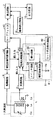
図2はこの発明の一実施形態の静電容量式検知装置の外観図である。図2において、円柱状の下部測定電極21は、筒状の上部測定電極22と接触しないように筒状の絶縁物で隔離されかつ上部測定電極21と絶縁物23とが同軸上に配置される。上部電極22の一端は取付具24を介して保護枠25に取付けられている。保護枠25内には後述の図1,図5などに示す回路部26が設けられていて、回路部26内には共振トランスも内蔵されている。
【0027】
図1はこの発明の一実施形態のブロック図である。図1において、共振回路1は電極体により形成される容量成分Cxと共振トランスLとの並列回路からなる。共振トランスLは1次コイルのインダクタンス成分Laと2次コイルのインダクタンス成分Lbとを含む。
【0028】
共振回路1の共振トランスLの2次コイルLbの出力は、変換回路2により、次段に適する信号に変換され、位相比較回路3の第1の入力端に与えられる。位相比較回路3は共振回路1からの出力信号と基準信号との位相を比較し、位相差に応じた位相差信号を出力する。この位相差信号は制御回路4と状態判別回路8とに与えられる。制御回路4は位相差信号に応じて共振回路1の出力信号と共振信号との位相差をなくすように制御信号を可変周波数発生回路5と検出回路7とに与える。
【0029】
可変周波数発生回路5はその制御信号に応じた発振周波数の発振信号を発生し、基準信号として位相比較回路3と駆動回路6とに与える。駆動回路6はその発振信号により共振回路1を駆動する。
【0030】
状態判別回路8は位相比較回路3の第2の入力端から与えられる位相差信号に基づいて、共振回路1の共振周波数と可変周波数発生回路5の発振周波数との間の位相差の有無を判別し、位相差が生じた場合に、その判別信号を位相比較回路3の第2の入力端と検出回路7とに与える。また、検出回路7には基準設定回路9から基準値が与えられる。検出回路7は制御回路4からの制御信号と基準設定回路によって設定された基準値とを比較して検出信号を出力する。出力回路10は検出回路7からの検出信号に応じて表示のための信号を出力する。
【0031】
図5はこの発明のより具体的な実施形態のブロック図である。この図5に示した実施形態は、以下の点を除いて図1と同じである。すなわち、可変周波数発生回路5として電圧制御発振回路(VCO)50が用いられる。電圧制御発振回路50は自走周波数fminから最高周波数fmaxまでの間の周波数で発振可能になっている。図1の制御回路4に代えてループフィルタ40が用いられる。状態判別回路8はリセット回路81とロック不良検出回路82とから構成されている。リセット回路81は積分回路83とスイッチ回路84と電圧比較回路85とを含む。
【0032】
積分回路83はループフィルタ40と同一回路で構成され、位相比較回路3から出力された位相差信号PCを直流電圧に変換して電圧比較回路85の第1の入力端に与える。電圧比較回路85の第2の入力端には電圧制御発振回路50の最高周波数fmaxに対応する直流電圧Vmaxよりわずかに低い周波数fsに対応した直流電圧Vsに設定された基準電圧が入力される。電圧比較回路85は積分回路83の出力の直流電圧が基準電圧Vsを上回ると、スイッチ回路84を導通させる。スイッチ回路84が導通すると、位相比較回路3の第1の入力端を短絡させる。ロック不良検出回路82は位相比較回路3から出力される非ロック信号LDに応じて検出回路7から検出信号を出力させる。
【0033】
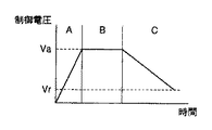
図6は位相比較回路の動作を説明するためのタイムチャートであり、図7は制御電圧の時間変化を示す図であり、図8は共振回路の共振周波数が変化した場合の発振周波数と制御信号の関係を示す図であり、図9は共振回路の共振周波数が可変周波数発生回路の可変周波数範囲を上回った場合の共振周波数の変化を時間的推移により示したグラフである。
【0034】
次に、図5〜図9を参照して、この発明のより具体的な実施形態の動作について説明する。被検出物がない状態でこの発明の静電容量式検知装置を容器などに設置し、電源を投入すると電源投入直後にはループフィルタ40は制御信号を発生しておらず、電圧制御発振回路50は共振回路1の共振周波数faに関係なく、自らの持つ自走周波数fminで発振を開始し、図6(b)に示すような発振信号を位相比較回路3の第2の入力端と駆動回路6とに与える。駆動回路6は共振回路1を駆動するのに十分なように発振信号を電力増幅し、増幅後の発振信号を共振回路1に供給する。
【0035】
共振回路1は駆動回路6により電圧制御発振回路50の自走周波数fminで発振する発振信号が入力されると、共振周波数faとの周波数差に対応して発振信号の位相をずらせて変換回路2に出力する。変換回路2は被検出物の誘電率が抵抗成分における振幅電圧に関係しないように位相成分のみを次段の位相比較回路3で扱うことができるように信号を変換し、図6(a)に示す信号を位相比較回路3の第1の入力端に与える。位相比較回路3は電圧制御発振回路50から駆動回路6を介して共振回路1に与えられ、変換回路2から第1の入力端に与えられる周波数fminの信号と、第2の入力端に電圧制御発振回路50から直接与えられている周波数fminの信号の位相を比較し、その位相差に対応した図6(c)に示す位相差信号PCをループフィルタ40に出力する。
【0036】
ループフィルタ40は位相差信号PCを積分して直流の制御信号に変換し、電圧制御発振回路50と検出回路7に出力する。以後、この動作を繰返し、位相差がなくなったとき、つまり電圧制御発振回路50の発振信号が共振回路1の共振周波数faと一致したとき、制御信号が図7に示すように一定電圧Vaとなり、その状態を保持する。したがって、校正に必要な作業をすることなく、電源投入により動作し、この状態となるまでの時間は瞬時であり、即座に完了する。
【0037】
上述の状態で、被検出物が電極体に接近または接触した場合などにおいて、共振回路1の共振周波数が電圧制御発振回路50が追従できる範囲(キャプチャレンジ)内の周波数frに変化した場合、電圧制御発振回路50の発振信号の周波数はfaであるため、共振回路1により周波数差に対応して位相がずれる。この位相ずれを位相比較回路3が検出し、ループフィルタ40の制御信号を応動させ、出力電圧を図7に示すようにVaからVrとすることにより、電圧制御発振回路50の発振信号の周波数をfrに一致させる。
【0038】
検出回路7はこの制御信号の電圧Vrを基準設定回路9の基準値Vcと比較し、Vr<Vcとなったとき、出力回路10に検知信号を出力する。出力回路10は検知信号により被検出物の検知を外部に出力または表示させる。
【0039】
被検出物が電極体に接近または接触した場合などにおいて、共振回路1の共振周波数が図8のfr′で示されるように電圧制御発振回路50が追従できる範囲(キャプチャレンジ)を下回った場合、電圧制御発振回路50の発振信号の周波数はfaであるため、共振回路1により周波数差に対応して位相がずれる。この位相ずれを位相比較回路3が検出し、ループフィルタ40の制御信号を応動させ、図7のCに示すように出力の直流電圧Vaを減少させ、電圧制御発振回路50の発振信号の周波数を低くさせるが、ループフィルタの制御信号が最小値0Vとなっても発振周波数fr′にすることができないため、この段階で固定され発振周波数は制御信号に対応したfminで固定される。
【0040】
検出回路7はこの制御信号を基準電圧Vcと比較し、被検出物の検知信号を出力回路10に出力する。出力回路10は検知信号により被検出物の検知を外部に出力または表示する。
【0041】
被検出物が電極体に接近または接触した場合などにおいて、共振回路1の共振周波数が図8のfr"で示されるように電圧制御発振回路50が追従できる範囲(キャプチャレンジ)を上回った場合、電圧制御発振回路50の発振信号の周波数はfaであるため、共振回路1により周波数差に対応して位相がずれる。
【0042】
この位相ずれを位相比較回路3が検出し、ループフィルタ40の制御信号を応動させ、その出力電圧をVaより増加させ、電圧制御発振回路50の発振信号の周波数を高くさせる。しかし、図9に示すように共振周波数fr"は発振信号の上限値fmaxよりも高いため、一致させることができず、発振信号がfmaxに固定されてしまう。
【0043】
そのため、積分回路83と電圧比較回路85とスイッチ回路84とから構成されるリセット回路81が設けられている。位相差信号PCはリセット回路81の積分回路83により直流信号に変換され、電圧比較回路85の第1の入力に入力される。電圧比較回路85の第2の入力はfmax時の直流信号Vmaxよりわずかに低い周波数fsに対応した電圧Vsに設定された基準電圧が入力される。積分回路83の直流信号が基準電圧Vsを上回ると、電圧比較回路85はスイッチ回路84を導通させる。
【0044】
スイッチ回路84が導通すると、位相比較回路3の第1の入力端が短絡され、位相比較回路3は比較すべき信号を失い、図6(c)に示すように位相差信号PCを0Vにする。位相差信号PCが0Vとなることで、ループフィルタ40の制御信号は0Vになり、電圧制御発振回路50は初期化され、発振信号の周波数をfminに設定すると同時に、リセット回路81の積分回路83の直流信号も0Vとなって基準電圧Vsを下回るため、電圧比較回路85はスイッチ回路84を開放し、位相比較回路3に第1の入力端が供給されるようにする。
【0045】
以下、位相比較,制御信号の増加,発振信号の周波数増加…というように上述の動作を繰返する。
【0046】
上述の動作を繰返している間は、図6(d)に示す位相比較回路3の位相差信号LDは非ロック信号をロック不良検出回路82に出力し、ロック不良検出回路82は非ロック信号が入力されることでスイッチ回路84を短絡して検出回路7の出力信号を被検出物の検知信号出力状態に固定する。
【0047】
被検出物の状態などが変化し、図8に示すように共振回路1の共振周波数がキャプチャレンジ内、たとえばfrに移動すると、前述の「被検出物が電極体に接近または接触した場合などにおいて、共振回路1の共振周波数が、電圧制御発振回路50が追従できる範囲(キャプチャレンジ)内の周波数frに変化した場合」と同様の動作により、電圧制御発振回路50は共振回路1の共振周波数frに一致した発振信号に同定され制御信号の電圧はVrとなる。
【0048】
積分回路83の直流信号は、リセット回路81の基準電圧Vsより低いため、リセット回路81のスイッチ回路84は開放状態を維持する。
【0049】
また、位相比較回路3の位相差信号LDは発振信号がfrに同定された時点でロック信号を出力するため、ロック不良検出回路82はスイッチ回路84を開放し、制御信号を検出回路7に入力させる。そのときの制御信号を検出回路7で判別し、被検出物の検知信号を出力回路に出力する。
【0050】
図10はこの発明の他の実施形態のブロック図である。この図10に示した実施形態は、図5に示した積分回路83をループフィルタ40に兼用させて積分回路83を省略し、部品点数を減らしたものである。このため、リセット回路86はスイッチ回路84と電圧比較回路85とによって構成され、電圧比較回路85の第2の入力端にはループフィルタ40の出力信号が与えられる。
【0051】
この図10に示した実施形態の具体的な動作は図5と同じであるため省略する。
【0052】
図11はこの発明のさらに他の実施形態を示すブロック図である。この図11に示した実施形態は、可変周波数発生回路50として、固定発振回路51と分周回路52とによって構成し、制御回路11と検出回路12と状態判別回路13をマイクロプロセッサ10で構成したものである。そして、マイクロプロセッサ10は位相比較回路3の出力信号を検知し、可変周波数発生回路50の分周回路52の分周比を制御する。
【0053】
ここで、マイクロプロセッサ10は可変周波数発生回路50の可変周波数の上限値および下限値に対応する分周回路52の分周比bmax,bminを予め設定する。固定発振回路51は所定の発振周波数で発振し、その信号を分周回路52に出力する。分周回路52はマイクロプロセッサ10に初期設定された分周比、たとえばbfminに従い、固定発振回路51の信号を分周した発振信号を駆動回路6を経由して共振回路1に送ると同時に位相比較回路3の第2の入力端に与える。共振回路1により位相が変化した信号は、変換回路2を介して位相比較回路3の第1の入力端に与えられる。
【0054】
位相比較回路3は第1の入力端と第2の入力端の信号を比較し、位相差がある場合は位相差信号LDに前述の図6(d)に示したような立下がりのパルス信号を発生させ、マイクロプロセッサ10に出力する。マイクロプロセッサ10はパルス信号が存在する間、分周比を順次変化、たとえば下限値から上限値まで単調増加を繰返すように変化させ、発振信号の周波数を増加させる。
【0055】
共振回路の共振周波数と発振周波数とが一致した場合、位相比較回路3は位相差信号LDにパルス信号を発生させないため、マイクロプロセッサ10はパルス信号がなくなった時点で分周回路52の分周比を固定し、発振信号を共振回路1の共振周波数と一致した値に固定すると同時に、その分周比に対応した値を記憶する。
【0056】
被検出物の状態に応答して、共振回路1の共振周波数はfrに変化した場合、マイクロプロセッサ10は上述の説明と同様の動作によりfrと一致した発振周波数に固定し、そのときの分周比に対応した値を記憶する。この記憶した値を基準設定回路9から得られる基準値と比較し、出力回路10に被検出物の検出状態信号を出力する。共振回路1の共振周波数は周波数可変範囲外(fr′,fr")となった場合は、マイクロプロセッサ10は分周比の下限および上限で規定される範囲で周波数を一定の繰返しで、たとえば単調増加を繰返すように変化させ続け、その間は出力回路10に被検出物の検出状態信号を出力させる。
【0057】
なお、前述の説明で予め設定する分周比の上下値および下限値を、電源投入時にマイクロプロセッサ10により可変できるような全周波数で掃引し、共振回路1の共振周波数を可変可能な全周波数の中央の値となるように分周回路52の分周比の上限値および下限値を設定し、記憶させるようにしてもよい。
【0058】
図12はこの発明のさらに他の実施形態を示すブロック図である。この図12に示した実施形態は、図11に示したマイクロプロセッサ10に警報出力用出力回路14と、メンテナンス用出力回路15と表示部16とを設けたものである。警報出力用出力回路15は電極体に被検出物が所定量以上付着したとき警報信号を出力する。メンテナンス用出力回路15は同様にしてメンテナンスのための信号を出力する。表示部16はたとえばLCD表示器からなり、空き時と動作時の周波数変化分(静電容量の変化分)を8段階で表示するものである。
【0059】
表示部16はたとえばLCD表示器などによって構成され、マイクロプロセッサ10が空き時と動作時の周波数変化分(静電容量の変化分)を検出し、LCD表示器に静電容量の変化分を8段階で表示させる。この表示機能を電極に付着した検出物の量の表示に利用でき、この表示を見て付着による誤動作の回避が可能となる。また付着の程度を設定することにより、電極部の清掃時期の出力が可能となる。
【0060】
図13は、この発明のさらに他の実施形態を示すブロック図である。
前述の図1に示した実施形態では、制御回路4から出力される制御電圧と基準値とを検出回路7で比較して被検出物の有無を検知するようにしたのに対して、この実施形態では、可変周波数発生回路5から出力される発振信号の周波数と基準設定回路9で設定されている基準値とを検出回路7で比較することにより被検出物の有無を検知するものであり、それ以外の構成は図1と同じである。
【0061】
このように検出回路7で周波数信号と基準値と比較する方が、制御電圧と基準値とを比較するよりもダイナミックレンジを大きくできるという利点がある。
【0062】
しかも、図1に示した実施形態では、位相比較回路3からの位相差信号を制御電圧に変換するときの温度特性が影響してくるのに対して、図13に示した例では純粋に共振回路1の共振周波数に応じた信号で基準値と比較するので、温度特性による影響を少なくできる。
【0063】
図14はこの発明のさらにその他の実施形態を示すブロック図である。
前述の図13に示した実施形態では、可変周波数発生回路5からの周波数信号と基準値とを比較して被検出物の有無を検知するようにしたが、この実施形態では可変周波数発生回路5からの周波数信号を分周回路18に与えて分周し、マイクロプロセッサ11で基準値と比較して被検出物の有無を検知する。
【0064】
図15は図14に示したマイクロプロセッサの動作を説明するためのフローチャートである。
【0065】
図15を参照して図14に示した静電容量式検知装置の動作について説明する。可変周波数発生回路5からの周波数信号は分周回路18によって分周されてマイクロプロセッサ11に与えられる。一方、マイクロプロセッサ11には、図示しないプッシュスイッチの操作やパーソナルコンピュータなどの通信によって、被検出物の状態が未検出状態かあるいは検出状態であるかが設定される。
【0066】
マイクロプロセッサ11は、未検出/検出が設定されたことに応じて現在の入力信号が検出時の周波数であるのかあるいは未検出時の周波数であるかの信号設定処理を行う。そして、マイクロプロセッサ11は、信号設定処理された検出時の周波数又は未検出時の周波数であれば、EEPROMなどのデータ保管メモリにこのデータを保管するための信号分別処理を行う。
【0067】
さらに、マイクロプロセッサ11は、信号分別処理で保管された周波数データと現在の周波数データとを比較し、未検出時の周波数<検出時の周波数≦現在の周波数であればONデータを出力し、現在の周波数<検出時の周波数であればOFFデータを出力する。
【0068】
一方、状態判別回路8から状態判別信号が出力されてマイクロプロセッサ11に与えられ、信号分別処理によって、適切な信号(チャッタリングなどのない信号)に変換された有無信号と現在の周波数との比較から出力されたデータによって、状態判別信号が有りであれば、現在の周波数との比較データに関わらずONデータを出力し、状態判別信号が無であれば、現在の周波数との比較データを出力する。
【0069】
そして、被検出物の有無の処理は、検出信号として必要な信号にタイマーを設けたり、検出時に出力信号を出力するのか、あるいは未検出時に出力信号を出力するのかを設定し、その設定にしたがって信号を出力する。
【0070】
また、現在の周波数との比較で、単純に周波数を比較するだけでなく、未検出時の周波数と検出時の周波数の間を等分割し、現在の周波数がどの位置あるのかを判定することにより、ONとOFFにヒステリシスを設けることも可能であり、前の周波数とも比較することにより、ノイズなどの影響を低減することも可能である。
【0071】
なお、今回開示された実施の形態はすべての点で例示であって制限的なものではないと考えられるべきである。本発明の範囲は上記した説明ではなく特許請求の範囲によって示され、特許請求の範囲と均等の意味および範囲内でのすべての変更が含まれることが意図される。
【0072】
【発明の効果】
以上のように、この発明によれば、共振手段と駆動手段と位相比較手段と可変周波数発生手段によってループを構成し、電源投入時に共振手段の共振周波数を探索し、その共振周波数で電極体を動作させるようにしたので、作業者が現場で校正作業をする必要が一切なくなり、人的ミスの発生の防止および作業効率の向上を可能にできる。
【0073】
また、検出動作時に共振手段の共振周波数を利用するため、検出感度のばらつきをなくすことができる。
【0074】
また、被検出物により共振手段の共振周波数が可変周波数発生手段の追従できる範囲(キャプチャレンジ)を超えたとしても使用可能であり、広範囲の使用条件に対応できる。
【0075】
さらに、被検出物の有無にかかわらず、共振手段の共振周波数で動作させ、周波数に対応した制御信号などによって検知するため、被検出物の導電性の影響を受けにくくすることができる。
【0076】
さらに、共振手段として並列共振回路を使用しているため、静電気に対して低インピーダンスとすることができ、耐静電気性能を向上できる。
【0077】
さらに、可変周波数発生手段を位相比較手段の第1および第2入力の周波数発生手段として兼用することにより、前置発振回路を不要としたことにより、コストダウンと故障率の低減を実現できる。
【0078】
さらに、使用部品の定格などを含めて回路部を共通にすることができるため、たとえばIC化などが可能となり、製作コストを低減できる。
【0079】
また、回路部が共通であることから、使用現場での予備品の種類を減らすことができ、経費を節減できる。
【図面の簡単な説明】
【図1】 この発明の一実施形態のブロック図である。
【図2】 この発明の一実施形態の静電容量式検知装置の外観図である。
【図3】 共振回路の等価回路図である。
【図4】 共振回路の周波数対振幅特性および周波数対位相特性を示す図である。
【図5】 この発明のより具体的な実施形態のブロック図である。
【図6】 位相比較回路の動作を説明するためのタイムチャートである。
【図7】 制御電圧の時間的変化を示す図である。
【図8】 共振回路の共振周波数が変化した場合の発振周波数と制御信号との関係を示す図である。
【図9】 共振回路の共振周波数が可変周波数発生回路の可変周波数範囲を上回った場合の共振周波数の変化を時間的推移により示したグラフである。
【図10】 この発明の他の実施形態のブロック図である。
【図11】 この発明のさらに他の実施形態を示すブロック図である。
【図12】 この発明のさらに他の実施形態を示すブロック図である。
【図13】 この発明のさらにその他の実施形態を示すブロック図である。
【図14】 この発明のさらにその他の実施形態を示すブロック図である。
【図15】 図14に示したマイクロプロセッサの動作を説明するためのフローチャートである。
【符号の説明】
1 共振回路、2 変換回路、3,30 位相比較回路、4,12 制御回路、5 可変周波数発生回路、6 駆動回路、7,13 検出回路、8,14 状態判別回路、9 基準設定回路、10 出力回路、11 マイクロプロセッサ、15 警報出力用出力回路、16 メンテナンス用出力回路、17 表示部、21 下部測定電極、22 上部測定電極、23 絶縁物、25 保護箱、26 回路部、40 ループフィルタ、50 電圧制御発振回路、51 固定発振回路、52 分周回路、81 リセット回路、82 ロック不良検出回路、83 積分回路、84 スイッチ回路、85 電圧比較回路。[0001]
BACKGROUND OF THE INVENTION
The present invention relates to a capacitance type detection device, for example, a detection object stored in a container such as a gas or a granular material is detected as a capacitance value by detecting a dielectric constant of the detection object as a capacitance value. The present invention relates to a capacitance type detection device.
[0002]
[Prior art]
Conventionally, when it is necessary to detect the level of an object to be detected, the detectable object has a wide range of applications such as liquid, powder, deposits in water, water and oil, etc. Capacitance type detection devices are used because there are no moving parts.
[0003]
However, the wide range of application of the object to be detected can be dealt with by changing each part, such as changing the electrode structure of the detection device or adding or changing circuit-use parts according to the usage environment. . In addition, since the electrostatic capacity due to the dielectric constant of the substance is measured, it is affected by the electrostatic capacity caused by the usage environment of the container, etc. It is necessary to calibrate with this, and the calibration work is very complicated. In addition, the operation may become unstable due to a change in the moisture content of the detection object due to moisture or the like, or a slight adhesion of the detection object having conductivity.
[0004]
In order to solve such a problem, Japanese Patent Application Laid-Open No. 59-54928 describes a capacitance type material level indicator. That is, the level indicator includes a fixed oscillation circuit, an amplifier circuit, a resonance circuit having an electrode body whose capacitance is changed by an object to be detected, a phase comparison circuit, an automatic calibration circuit having a switch, an output circuit, The oscillation signal of the fixed oscillation circuit is supplied to the resonance circuit as an excitation signal through the amplifier circuit, and the phase difference of the excitation signal whose phase has changed between the oscillation signal and the resonance circuit is detected by the phase comparison circuit. A corresponding detection signal is provided to the automatic calibration circuit. The automatic calibration circuit changes the operation characteristics of the resonance circuit step by step so that the detection signal matches the reference signal when the switch is pressed. Further, by performing an operation of changing the reference signal so that the reference signal coincides with the detection signal, the application to the detection object and the calibration work are easily performed.
[0005]
However, this method requires a calibration work even if the switch is simply pressed on site, and does not operate normally if the operator neglects the calibration work. In addition, when it is necessary to change the installation location, it is necessary to perform calibration work each time. Further, it is difficult to use the resonance state of the resonance circuit, and the detection sensitivity may vary.
[0006]
As another example, Japanese Patent Application Laid-Open No. 5-87612 discloses a liquid level detecting device using a PLL circuit. That is, in this example, a PLL circuit is configured by a phase comparison circuit, a loop filter (integration circuit), and a voltage controlled oscillation circuit (VCO circuit), and the pre-oscillation circuit is oscillated at an oscillation frequency in response to an object to be detected. The oscillation frequency signal is input to the phase comparison circuit of the PLL circuit, and the detected object is detected by comparing the frequency with the frequency signal of the VCO circuit.
[0007]
[Problems to be solved by the invention]
However, in the above-described second example, it is necessary to satisfy the following predetermined conditions.
[0008]
(1) When there is no object to be detected, the oscillation frequency of the pre-oscillation circuit is outside the lock range of the PLL circuit. When the object to be detected is in contact with or close to the object, the oscillation frequency of the pre-oscillation circuit is within the lock range of the PLL circuit. Set to be.
[0009]
(2) The oscillation frequency of the pre-oscillation circuit is within the lock range of the PLL circuit when there is no object to be detected, and the oscillation frequency of the pre-oscillation circuit is outside the lock range of the PLL circuit when the object to be detected contacts or approaches. Set to be.
[0010]
(3) Either of the cases where the oscillation frequency of the pre-oscillation circuit is set to be within the lock range of the PLL circuit both when there is no detection object and when the detection object is in contact with or approaching Set up.
[0011]
To set the frequency change range of the pre-oscillation circuit and the lock range of the PLL circuit to meet the limited conditions, it is necessary to consider the site of use and the object to be detected, which is very complicated. Become. In other words, the scope of application is limited.
[0012]
Therefore, the main object of the present invention is that no calibration work is required, the handling of the operator is simple, variation in detection sensitivity is eliminated, and it is possible to cope with a wide range of use conditions. It is an object of the present invention to provide a capacitance type detection device that is not easily affected and is strong against static electricity.
[0013]
[Means for Solving the Problems]
The invention according to claim 1 is an electrostatic capacitance type detection device, and is formed by an electrode body configured in an appropriate form such as a rod shape so as to respond to the electrostatic capacity of an object to be detected in a container, and the electrode body A resonance unit including a resonance transformer for tuning with a capacitance to be compared, a phase comparison unit that compares a phase of an output signal of the resonance unit and a reference signal, and outputs a phase difference signal corresponding to the phase difference; Control means for outputting a control signal for eliminating the phase difference in accordance with the phase difference signal from the comparison means, and a variable frequency for generating a frequency signal having an oscillation frequency in accordance with the control signal from the control means and providing the phase comparison means Generating means, driving means for driving the electrode body with a frequency signal from the variable frequency generating means, reference value setting means for setting a reference value in the detection state of the detected object, and a control signal output from the control means Or variable lap The detection means for outputting a detection signal by comparing the frequency signal output from the number generation means with the reference value set by the reference value setting means, and outputting a display signal in accordance with the detection signal of the detection means If there is a phase difference by determining whether or not there is a phase difference between the resonance frequency of the resonance means and the oscillation frequency of the variable frequency generation means based on the phase difference signal output from the output means and the phase comparison means And a state determining means for setting the variable frequency generating means and the detecting means to a predetermined state.
[0014]
According to a second aspect of the present invention, the state discriminating means of the first aspect uses the frequency signal of the variable frequency generating means as the variable frequency in response to the phase difference signal output from the phase comparing means being equal to or greater than a predetermined value. The reset means for setting the frequency variable of the generating means to the lowest variable frequency and the phase of the oscillation frequency of the variable frequency generating means are compared with the phase of the resonant frequency of the resonant means, and if they do not match, a detection signal is output from the detecting means Locking failure detection means.
[0015]
According to a third aspect of the present invention, the reset means of the second aspect includes an integration circuit that integrates the phase difference signal output from the phase comparison means, and a voltage comparison that compares the integration signal from the integration circuit with a predetermined voltage value. And a switching means for setting the oscillation frequency of the variable frequency generating means to the lowest frequency when it is determined by the voltage comparison circuit that the integrated signal is equal to or higher than a predetermined voltage value.
[0016]
In the invention according to claim 4, the control means of claim 1 includes a loop filter.
In the invention according to
[0017]
In the invention according to
[0018]
In the invention according to claim 7, the control means, the detection means, and the state determination means are constituted by a microprocessor.
[0019]
According to an eighth aspect of the present invention, there is provided an electrode body configured in an appropriate shape such as a rod shape so as to respond to the electrostatic capacity of an object to be detected in the container, and for synchronizing with the electrostatic capacity formed by the electrode body. A resonance means including a resonance transformer, a phase comparison means for comparing the phase of the output signal of the resonance means and a reference signal, and outputting a phase difference signal according to the phase difference, and a phase according to the phase difference signal from the phase comparison means; A control means for outputting a control signal for eliminating the phase difference, a variable frequency generating means for generating a frequency signal having an oscillation frequency corresponding to the control signal from the control means and supplying the signal to the phase comparing means, and a frequency from the variable frequency generating means A driving means for driving the electrode body with a signal, a reference value setting means for setting a reference value in a detection state of the detection object, a control signal output from the control means, and a reference set by the reference value setting means The The detection means for outputting the detection signal in comparison, the display means for displaying the change in the capacitance stepwise according to the detection signal, and the resonance frequency of the resonance means based on the phase difference signal output from the phase comparison means And a state discriminating means for setting the variable frequency generating means and the detecting means to a predetermined state when a phase difference occurs. The
[0020]
According to a ninth aspect of the present invention, the detection means of the first aspect includes a microprocessor, and the microprocessor detects whether or not the state of the detected object is a detection state, and a detection state setting means. Signal processing setting means for setting whether or not it is a frequency at the time of detection according to whether it is set, and storage means for storing the set frequency at the time of detection or the frequency at the time of detection A comparison means for comparing the stored frequency with the current frequency given from the variable frequency generation means, and outputting data indicating whether the current frequency is higher than the frequency at the time of detection, and a state determination means Includes means for outputting data with an object to be detected in response to a signal having a phase difference from, and outputting data from a comparing means in response to a signal having no phase difference. This And wherein the
[0021]
DETAILED DESCRIPTION OF THE INVENTION
First, a resonance circuit used in the present invention will be described before describing an embodiment of the present invention.
[0022]
FIG. 3 is an equivalent circuit diagram of the resonance circuit, and FIG. 4 is a diagram showing frequency vs. amplitude characteristics and frequency vs. phase characteristics of the resonance circuit.
[0023]
As shown in FIG. 3, the resonance circuit includes a parallel circuit of a capacitor component Cx formed by an electrode plate and an inductance component La of the resonance transformer. The resonance frequency of the resonance circuit is expressed by the following equation.
[0024]
fa = 1 / {2π√ (LaCx)}
As is apparent from this equation, the resonance frequency does not depend on the resistance component Rx. Further, as shown in FIG. 4A, since the impedance is low in the low frequency region, it has a characteristic that the impedance is low with respect to the capacitance.
[0025]
4 (a) and 4 (b), the frequency and phase of the resonance circuit have a correlation, and no phase difference occurs when the resonance frequency is input, and the frequency is lower as a frequency lower than the resonance frequency is input. The phase difference approaches 90 °, and approaches −90 ° as a frequency higher than the resonance frequency is input, and the degree of phase change becomes steep near the resonance frequency. In FIG. 4, fa represents the resonance frequency when the electrode body is in the air, and fr represents the resonance frequency when the object to be detected is close to or in contact with the electrode body. The value of the phase angle also changes at the same time as the resonance frequency of the resonance circuit changes due to the movement of the detected object.
[0026]
Hereinafter, embodiments will be specifically described.
FIG. 2 is an external view of a capacitance type detection device according to an embodiment of the present invention. In FIG. 2, a cylindrical
[0027]
FIG. 1 is a block diagram of an embodiment of the present invention. In FIG. 1, a resonance circuit 1 is composed of a parallel circuit of a capacitive component Cx formed by an electrode body and a resonance transformer L. The resonant transformer L includes an inductance component La of the primary coil and an inductance component Lb of the secondary coil.
[0028]
The output of the secondary coil Lb of the resonance transformer L of the resonance circuit 1 is converted into a signal suitable for the next stage by the
[0029]
The variable
[0030]
The
[0031]
FIG. 5 is a block diagram of a more specific embodiment of the present invention. The embodiment shown in FIG. 5 is the same as FIG. 1 except for the following points. That is, a voltage controlled oscillation circuit (VCO) 50 is used as the variable
[0032]
The integrating
[0033]
FIG. 6 is a time chart for explaining the operation of the phase comparison circuit, FIG. 7 is a diagram showing a time change of the control voltage, and FIG. 8 is an oscillation frequency and control signal when the resonance frequency of the resonance circuit changes. FIG. 9 is a graph showing the change in the resonance frequency over time when the resonance frequency of the resonance circuit exceeds the variable frequency range of the variable frequency generation circuit.
[0034]
Next, the operation of a more specific embodiment of the present invention will be described with reference to FIGS. When the capacitive sensing device of the present invention is installed in a container or the like in the absence of an object to be detected and the power is turned on, the
[0035]
When the oscillation circuit that oscillates at the free-running frequency fmin of the voltage controlled
[0036]
The
[0037]
When the object to be detected approaches or comes into contact with the electrode body in the above-described state, when the resonance frequency of the resonance circuit 1 changes to the frequency fr within the range (capture range) that the voltage-controlled
[0038]
The detection circuit 7 compares the voltage Vr of the control signal with the reference value Vc of the
[0039]
When the object to be detected approaches or contacts the electrode body, the resonance frequency of the resonance circuit 1 falls below the range (capture range) that the voltage controlled
[0040]
The detection circuit 7 compares this control signal with the reference voltage Vc, and outputs a detection signal of the detected object to the
[0041]
When the object to be detected approaches or contacts the electrode body, the resonance frequency of the resonance circuit 1 exceeds the range (capture range) that the voltage controlled
[0042]
This phase shift is detected by the
[0043]
Therefore, a
[0044]
When the
[0045]
Thereafter, the above operations are repeated, such as phase comparison, increase in control signal, increase in frequency of oscillation signal, and so on.
[0046]
While the above operation is repeated, the phase difference signal LD of the
[0047]
When the state of the object to be detected changes and the resonance frequency of the resonance circuit 1 moves within the capture range, for example, fr as shown in FIG. 8, the above-mentioned “in the case where the object to be detected approaches or contacts the electrode body” The voltage-controlled
[0048]
Since the DC signal of the
[0049]
Since the phase difference signal LD of the
[0050]
FIG. 10 is a block diagram of another embodiment of the present invention. In the embodiment shown in FIG. 10, the integrating
[0051]
The specific operation of the embodiment shown in FIG. 10 is the same as that in FIG.
[0052]
FIG. 11 is a block diagram showing still another embodiment of the present invention. In the embodiment shown in FIG. 11, the variable
[0053]
Here, the
[0054]
The
[0055]
When the resonance frequency and the oscillation frequency of the resonance circuit coincide with each other, the
[0056]
When the resonance frequency of the resonance circuit 1 changes to fr in response to the state of the object to be detected, the
[0057]
Note that the upper and lower limits and the lower limit of the frequency division ratio set in advance in the above description are swept at all frequencies that can be varied by the
[0058]
FIG. 12 is a block diagram showing still another embodiment of the present invention. In the embodiment shown in FIG. 12, a
[0059]
The
[0060]
FIG. 13 is a block diagram showing still another embodiment of the present invention.
In the embodiment shown in FIG. 1 described above, the control voltage output from the control circuit 4 and the reference value are compared by the detection circuit 7 to detect the presence or absence of an object to be detected. In the embodiment, the detection circuit 7 detects the presence or absence of an object to be detected by comparing the frequency of the oscillation signal output from the variable
[0061]
Thus, comparing the frequency signal with the reference value by the detection circuit 7 has an advantage that the dynamic range can be increased compared with comparing the control voltage with the reference value.
[0062]
Moreover, in the embodiment shown in FIG. 1, the temperature characteristic when the phase difference signal from the
[0063]
FIG. 14 is a block diagram showing still another embodiment of the present invention.
In the embodiment shown in FIG. 13, the frequency signal from the variable
[0064]
FIG. 15 is a flowchart for explaining the operation of the microprocessor shown in FIG.
[0065]
The operation of the capacitive sensing device shown in FIG. 14 will be described with reference to FIG. The frequency signal from the variable
[0066]
The
[0067]
Further, the
[0068]
On the other hand, a state determination signal is output from the
[0069]
In addition, in the processing of the presence / absence of an object to be detected, a timer is provided for a signal necessary as a detection signal, an output signal is output when detected, or an output signal is output when not detected, and according to the setting Output a signal.
[0070]
Also, by comparing with the current frequency, not only simply comparing the frequency, but also dividing the frequency between the undetected frequency and the detected frequency equally to determine where the current frequency is. It is also possible to provide hysteresis for ON and OFF, and it is also possible to reduce the influence of noise and the like by comparing with the previous frequency.
[0071]
The embodiment disclosed this time should be considered as illustrative in all points and not restrictive. The scope of the present invention is defined by the terms of the claims, rather than the description above, and is intended to include any modifications within the scope and meaning equivalent to the terms of the claims.
[0072]
【The invention's effect】
As described above, according to the present invention, the resonance means, the drive means, the phase comparison means, and the variable frequency generation means constitute a loop, and the resonance frequency of the resonance means is searched when the power is turned on. Since it is made to operate, it is no longer necessary for the operator to perform calibration work at the site, and it is possible to prevent the occurrence of human error and improve work efficiency.
[0073]
Further, since the resonance frequency of the resonance means is used during the detection operation, variations in detection sensitivity can be eliminated.
[0074]
Further, even if the resonance frequency of the resonance means exceeds the range (capture range) that can be followed by the variable frequency generation means due to the object to be detected, it can be used and can cope with a wide range of use conditions.
[0075]
Furthermore, regardless of the presence or absence of the object to be detected, the resonance means is operated at the resonance frequency and detected by a control signal or the like corresponding to the frequency, so that it is difficult to be influenced by the conductivity of the object to be detected.
[0076]
Furthermore, since the parallel resonant circuit is used as the resonance means, the impedance can be reduced with respect to static electricity, and the anti-static performance can be improved.
[0077]
Further, by using the variable frequency generation means as the frequency generation means for the first and second inputs of the phase comparison means, the pre-oscillation circuit is not required, thereby reducing the cost and reducing the failure rate.
[0078]
Furthermore, since the circuit portion including the ratings of the parts used can be made common, for example, it is possible to make an IC, and the manufacturing cost can be reduced.
[0079]
In addition, since the circuit portion is common, the types of spare parts at the use site can be reduced, and the cost can be reduced.
[Brief description of the drawings]
FIG. 1 is a block diagram of an embodiment of the present invention.
FIG. 2 is an external view of a capacitance type detection device according to an embodiment of the present invention.
FIG. 3 is an equivalent circuit diagram of a resonance circuit.
FIG. 4 is a diagram showing frequency vs. amplitude characteristics and frequency vs. phase characteristics of a resonant circuit.
FIG. 5 is a block diagram of a more specific embodiment of the present invention.
FIG. 6 is a time chart for explaining the operation of the phase comparison circuit;
FIG. 7 is a diagram showing temporal changes in control voltage.
FIG. 8 is a diagram illustrating a relationship between an oscillation frequency and a control signal when the resonance frequency of the resonance circuit changes.
FIG. 9 is a graph showing changes in resonance frequency over time when the resonance frequency of the resonance circuit exceeds the variable frequency range of the variable frequency generation circuit.
FIG. 10 is a block diagram of another embodiment of the present invention.
FIG. 11 is a block diagram showing still another embodiment of the present invention.
FIG. 12 is a block diagram showing still another embodiment of the present invention.
FIG. 13 is a block diagram showing still another embodiment of the present invention.
FIG. 14 is a block diagram showing still another embodiment of the present invention.
15 is a flowchart for explaining the operation of the microprocessor shown in FIG. 14; FIG.
[Explanation of symbols]
DESCRIPTION OF SYMBOLS 1 Resonance circuit, 2 Conversion circuit, 3,30 Phase comparison circuit, 4,12 Control circuit, 5 Variable frequency generation circuit, 6 Drive circuit, 7,13 Detection circuit, 8, 14 State discrimination circuit, 9 Reference setting circuit, 10
Claims (8)
前記電極体により形成される静電容量と同調するための共振トランスを含む共振手段、
前記共振手段の出力信号と基準信号との位相を比較し、位相差に応じた位相差信号を出力する位相比較手段、
前記位相比較手段からの位相差信号に応じて前記位相差をなくすための制御信号を出力する制御手段、
前記制御手段からの制御信号に応じた発振周波数の周波数信号を発生して、前記位相比較手段に与える可変周波数発生手段、
前記可変周波数発生手段からの周波数信号で前記電極体を駆動するための駆動手段、
前記被検出物の検出状態における基準値を設定する基準値設定手段、
前記制御手段から出力される制御信号または前記可変周波数発生手段から出力される周波数信号と、前記基準値設定手段によって設定された基準値とを比較して検出信号を出力する検出手段、
前記検出手段の検出信号に応じて表示のための信号を出力する出力手段、および
前記位相比較手段から出力される位相差信号に基づいて、前記共振手段の共振周波数と前記可変周波数発生手段の発振周波数との間の位相差の有無を判別し、位相差が生じた場合に前記可変周波数発生手段と前記検出手段を所定の状態に設定する状態判別手段を備え、
前記状態判別手段は、
前記位相比較手段から出力された位相差信号が所定の値以上になったことに応じて、前記可変周波数発生手段の周波数信号を該可変周波数発生手段の周波数可変の最低周波数に設定するリセット手段と、
前記可変周波数発生手段の発振周波数の位相を前記共振手段の共振周波数の位相と比較し、一致していない場合に前記検出手段から検出信号を出力させるロック不良検出手段とを含む、静電容量式検知装置。An electrode body configured in an appropriate form such as a rod so as to respond to the capacitance of the object to be detected in the container,
Resonance means including a resonance transformer for tuning with the capacitance formed by the electrode body;
A phase comparison means for comparing the phase of the output signal of the resonance means and a reference signal and outputting a phase difference signal corresponding to the phase difference;
Control means for outputting a control signal for eliminating the phase difference according to the phase difference signal from the phase comparison means;
A variable frequency generating means for generating a frequency signal having an oscillation frequency in accordance with a control signal from the control means and supplying the frequency signal to the phase comparing means;
Driving means for driving the electrode body with a frequency signal from the variable frequency generating means;
Reference value setting means for setting a reference value in the detection state of the detected object;
Detection means for comparing the control signal output from the control means or the frequency signal output from the variable frequency generation means with the reference value set by the reference value setting means, and outputting a detection signal;
Output means for outputting a signal for display according to the detection signal of the detection means; and oscillation of the resonance frequency of the resonance means and the variable frequency generation means based on the phase difference signal output from the phase comparison means Determining whether or not there is a phase difference between frequencies, and including a state determining unit that sets the variable frequency generating unit and the detecting unit to a predetermined state when a phase difference occurs ;
The state determination means includes
Resetting means for setting the frequency signal of the variable frequency generating means to the lowest variable frequency of the variable frequency generating means in response to the phase difference signal output from the phase comparing means being equal to or greater than a predetermined value; ,
A capacitance failure detection means for comparing the phase of the oscillation frequency of the variable frequency generation means with the phase of the resonance frequency of the resonance means, and outputting a detection signal from the detection means if they do not match. Detection device.
前記位相比較手段から出力される位相差信号を積分する積分手段と、
前記積分手段からの積分信号と所定の電圧値とを比較する電圧比較手段と、
前記電圧比較手段によって前記積分信号が前記所定の電圧値以上であることが判別されたことに応じて、前記可変周波数発生手段の発振周波数を前記最低周波数に設定するスイッチング手段とを含む、請求項1に記載の静電容量式検知装置。The reset means includes
Integrating means for integrating the phase difference signal output from the phase comparing means;
Voltage comparison means for comparing the integration signal from the integration means with a predetermined voltage value;
Switching means for setting the oscillation frequency of the variable frequency generating means to the lowest frequency when the voltage comparing means determines that the integrated signal is equal to or higher than the predetermined voltage value. 1. The capacitance type detection device according to 1.
固定の周波数信号を発生する固定発振手段と、
前記制御手段からの制御信号に応じて、その分周比が可変に設定され、設定された分周比で前記固定発振手段から発生された周波数信号を分周して出力する分周手段とを備えた、請求項1に記載の静電容量式検知装置。The variable frequency generating means includes
Fixed oscillation means for generating a fixed frequency signal;
A frequency dividing means that variably sets the frequency dividing ratio according to a control signal from the control means, and divides and outputs the frequency signal generated from the fixed oscillating means with the set frequency dividing ratio; The electrostatic capacity type detection device according to claim 1 provided.
前記電極体により形成される静電容量と同調するための共振トランスを含む共振手段、
前記共振手段の出力信号と基準信号との位相を比較し、位相差に応じた位相差信号を出力する位相比較手段、
前記位相比較手段からの位相差信号に応じて前記位相差をなくすための制御信号を出力する制御手段、
前記制御手段からの制御信号に応じた発振周波数の周波数信号を発生して、前記位相比較手段に与える可変周波数発生手段、
前記可変周波数発生手段からの周波数信号で前記電極体を駆動するための駆動手段、
前記被検出物の検出状態における基準値を設定する基準値設定手段、
前記制御手段から出力される制御信号と前記基準値設定手段によって設定された基準値とを比較して検出信号を出力する検出手段、
前記検出手段の検出信号に応じて前記静電容量の変化を段階的に表示する表示手段、および
前記位相比較手段から出力される位相差信号に基づいて、前記共振手段の共振周波数と前記可変周波数発生手段の発振周波数との間の位相差の有無を判別し、位相差が生じた場合に前記可変周波数発生手段と前記検出手段を所定の状態に設定する状態判別手段を備え、
前記状態判別手段は、
前記位相比較手段から出力された位相差信号が所定の値以上になったことに応じて、前記可変周波数発生手段の周波数信号を該可変周波数発生手段の周波数可変の最低周波数に設定するリセット手段と、
前記可変周波数発生手段の発振周波数の位相を前記共振手段の共振周波数の位相と比較し、一致していない場合に前記検出手段から検出信号を出力させるロック不良検出手段とを含む、静電容量式検知装置。An electrode body configured in an appropriate form such as a rod so as to respond to the capacitance of the object to be detected in the container,
Resonance means including a resonance transformer for tuning with the capacitance formed by the electrode body;
A phase comparison means for comparing the phase of the output signal of the resonance means and a reference signal and outputting a phase difference signal corresponding to the phase difference;
Control means for outputting a control signal for eliminating the phase difference according to the phase difference signal from the phase comparison means;
A variable frequency generating means for generating a frequency signal having an oscillation frequency in accordance with a control signal from the control means and supplying the frequency signal to the phase comparing means;
Driving means for driving the electrode body with a frequency signal from the variable frequency generating means;
Reference value setting means for setting a reference value in the detection state of the detected object;
Detecting means for comparing the control signal output from the control means with the reference value set by the reference value setting means and outputting a detection signal;
Display means for displaying the change in capacitance in a stepwise manner according to the detection signal of the detection means, and the resonance frequency and the variable frequency of the resonance means based on the phase difference signal output from the phase comparison means Determining whether or not there is a phase difference from the oscillation frequency of the generating means, and comprising a state determining means for setting the variable frequency generating means and the detecting means to a predetermined state when a phase difference occurs,
The state determination means includes
Resetting means for setting the frequency signal of the variable frequency generating means to the lowest variable frequency of the variable frequency generating means in response to the phase difference signal output from the phase comparing means being equal to or greater than a predetermined value; ,
A capacitance failure detection means for comparing the phase of the oscillation frequency of the variable frequency generation means with the phase of the resonance frequency of the resonance means, and outputting a detection signal from the detection means if they do not match. Detection device.
前記マイクロプロセッサは、
前記被検出物の状態が検出状態であるか否かを設定するための検出状態設定手段と、
前記検出状態設定手段によって検出状態であることが設定されているかに応じて、検出時の周波数であるか否かを設定するための信号処理設定手段と、
前記信号処理設定手段によって設定された検出時の周波数または被検出時の周波数を記憶する記憶手段と、
前記記憶手段に記憶されている周波数と前記可変周波数発生手段から与えられる現在の周波数とを比較し、現在の周波数が検出時の周波数よりも高いか否かを示すデータを出力する比較手段と、
前記状態判別手段から位相差ありの信号が与えられたことに応じて、被検出物ありのデータを出力し、位相差なしの信号が与えられたことに応じて、前記比較手段からのデータを出力する手段を含むことを特徴とする、請求項1に記載の静電容量式検知装置。The detection means includes a microprocessor;
The microprocessor is
Detection state setting means for setting whether or not the state of the detection object is a detection state;
Signal processing setting means for setting whether or not it is a frequency at the time of detection, depending on whether the detection state is set by the detection state setting means;
Storage means for storing the frequency at the time of detection or the frequency at the time of detection set by the signal processing setting means;
Comparing means for comparing the frequency stored in the storage means with the current frequency given from the variable frequency generating means, and outputting data indicating whether the current frequency is higher than the frequency at the time of detection;
In response to a signal having a phase difference from the state determining means, data having an object to be detected is output, and in response to a signal having no phase difference, the data from the comparing means is output. The electrostatic capacity type detection device according to claim 1, further comprising means for outputting.
Priority Applications (5)
| Application Number | Priority Date | Filing Date | Title |
|---|---|---|---|
| JP2000076027A JP4497637B2 (en) | 1999-11-01 | 2000-03-17 | Capacitance type detection device |
| US09/617,134 US6292104B1 (en) | 1999-11-01 | 2000-07-14 | Capacitance type detector |
| DE60000566T DE60000566T2 (en) | 1999-11-01 | 2000-07-19 | The capacitance |
| KR10-2000-0041313A KR100421573B1 (en) | 1999-11-01 | 2000-07-19 | Capacitance type detector |
| EP00115586A EP1096238B1 (en) | 1999-11-01 | 2000-07-19 | Capacitance type detector |
Applications Claiming Priority (3)
| Application Number | Priority Date | Filing Date | Title |
|---|---|---|---|
| JP31126799 | 1999-11-01 | ||
| JP11-311267 | 1999-11-01 | ||
| JP2000076027A JP4497637B2 (en) | 1999-11-01 | 2000-03-17 | Capacitance type detection device |
Publications (2)
| Publication Number | Publication Date |
|---|---|
| JP2001194207A JP2001194207A (en) | 2001-07-19 |
| JP4497637B2 true JP4497637B2 (en) | 2010-07-07 |
Family
ID=26566652
Family Applications (1)
| Application Number | Title | Priority Date | Filing Date |
|---|---|---|---|
| JP2000076027A Expired - Lifetime JP4497637B2 (en) | 1999-11-01 | 2000-03-17 | Capacitance type detection device |
Country Status (5)
| Country | Link |
|---|---|
| US (1) | US6292104B1 (en) |
| EP (1) | EP1096238B1 (en) |
| JP (1) | JP4497637B2 (en) |
| KR (1) | KR100421573B1 (en) |
| DE (1) | DE60000566T2 (en) |
Families Citing this family (22)
| Publication number | Priority date | Publication date | Assignee | Title |
|---|---|---|---|---|
| US8026729B2 (en) | 2003-09-16 | 2011-09-27 | Cardiomems, Inc. | System and apparatus for in-vivo assessment of relative position of an implant |
| US20050187482A1 (en) | 2003-09-16 | 2005-08-25 | O'brien David | Implantable wireless sensor |
| US7245117B1 (en) * | 2004-11-01 | 2007-07-17 | Cardiomems, Inc. | Communicating with implanted wireless sensor |
| EP1637875A1 (en) * | 2004-09-17 | 2006-03-22 | Fondazione Torino Wireless | A multi-frequency capacitive measurement device and a method of operating the same |
| WO2007002185A2 (en) | 2005-06-21 | 2007-01-04 | Cardiomems, Inc. | Method of manufacturing implantable wireless sensor for in vivo pressure measurement |
| US7821411B1 (en) | 2006-02-09 | 2010-10-26 | Diversitech Corporation | Safety device for monitoring a conduit |
| US7711509B2 (en) * | 2007-03-29 | 2010-05-04 | The United States Of America As Represented By The Administrator Of The National Aeronautics And Space Administration | Method of calibrating a fluid-level measurement system |
| US8022775B2 (en) * | 2009-10-08 | 2011-09-20 | Etymotic Research, Inc. | Systems and methods for maintaining a drive signal to a resonant circuit at a resonant frequency |
| GB201019683D0 (en) * | 2010-11-19 | 2011-01-05 | Domino Printing Sciences Plc | Improvements in or relating to inkjet printers |
| RU2463565C1 (en) * | 2011-06-01 | 2012-10-10 | Михаил Михайлович РУМЯНЦЕВ | Apparatus for measuring and indicating limiting level of liquid oil in non-transparent containers |
| RU2597067C1 (en) * | 2015-05-20 | 2016-09-10 | Михаил Михайлович РУМЯНЦЕВ | Device for measurement and indication of limiting level of liquid oils, liquefied natural gas in opaque reservoirs |
| WO2016208382A1 (en) * | 2015-06-25 | 2016-12-29 | 新東工業株式会社 | Surface characteristic evaluation apparatus and surface characteristic evaluation method for steel material |
| HUE040669T2 (en) * | 2015-07-15 | 2019-03-28 | Grieshaber Vega Kg | Fill level measurement device |
| KR102409776B1 (en) * | 2015-08-06 | 2022-06-16 | 엘지이노텍 주식회사 | Wiper driving device and metohd for driving thereof |
| US10072962B2 (en) * | 2016-07-05 | 2018-09-11 | Ecolab Usa Inc. | Liquid out-of-product alarm system and method |
| US10509378B2 (en) * | 2016-11-07 | 2019-12-17 | FarmX Inc. | Systems and methods for soil modeling and automatic irrigation control |
| JP6542188B2 (en) * | 2016-12-27 | 2019-07-10 | シーエル計測工業株式会社 | Object detection sensor |
| JP6678198B2 (en) * | 2018-05-23 | 2020-04-08 | シーエル計測工業株式会社 | Object detection sensor |
| JP6725588B2 (en) * | 2018-05-23 | 2020-07-22 | シーエル計測工業株式会社 | Object detection sensor |
| EP3897905B1 (en) * | 2018-11-21 | 2024-03-27 | Cameron Technologies Limited | Power unit phase angle for separation unit control |
| DE102021101417A1 (en) | 2021-01-22 | 2022-07-28 | Vega Grieshaber Kg | Process for point level detection and point level sensor |
| RU2759394C1 (en) * | 2021-03-05 | 2021-11-12 | федеральное государственное бюджетное образовательное учреждение высшего образования "Алтайский государственный технический университет им. И.И. Ползунова" (АлтГТУ) | Power transformer oil level control device |
Family Cites Families (15)
| Publication number | Priority date | Publication date | Assignee | Title |
|---|---|---|---|---|
| JPS56129819A (en) * | 1980-03-18 | 1981-10-12 | Nippon Kokan Kk <Nkk> | Eddy current type mold level meter with agc |
| JPS645206Y2 (en) * | 1981-05-30 | 1989-02-09 | ||
| US5245873A (en) * | 1982-08-25 | 1993-09-21 | Berwind Corporation | Capacitance-type material level indicator and method of operation |
| US4499640A (en) | 1982-08-25 | 1985-02-19 | Berwind Corporation | Method of manufacturing capacitance-type material level indicator probe |
| JPH0785031B2 (en) * | 1986-05-23 | 1995-09-13 | 株式会社ノーケン | Capacitance type level detector |
| JP2516780B2 (en) * | 1987-04-17 | 1996-07-24 | 本田技研工業株式会社 | Bad road detection device when the vehicle is running |
| US4912976A (en) | 1987-06-26 | 1990-04-03 | Beckman Instruments, Inc. | Liquid level sensing apparatus |
| US5265482A (en) * | 1991-05-21 | 1993-11-30 | E. I. Du Pont De Nemours And Company | Method of sampling a container |
| IT1255653B (en) * | 1991-08-08 | 1995-11-09 | SENSOR FOR ELECTROCHEMICAL MEASUREMENTS | |
| JPH0587612A (en) * | 1991-09-27 | 1993-04-06 | Jiyaruko:Kk | Detector for liquid body level using pll circuit |
| JPH05180795A (en) * | 1992-01-08 | 1993-07-23 | Jiyaruko:Kk | Detector using pll circuit for foreign matters mixed into normal matter being transferred through passage |
| JPH06258127A (en) * | 1992-12-25 | 1994-09-16 | Nikko Co Ltd | Capacitance type level meter |
| JP3421122B2 (en) * | 1994-05-11 | 2003-06-30 | 株式会社ノーケン | Capacitive sensing device |
| JPH0851336A (en) * | 1994-08-03 | 1996-02-20 | Sony Tektronix Corp | Low-pass filter capable of automatic calibration |
| US5973415A (en) * | 1997-08-28 | 1999-10-26 | Kay-Ray/Sensall, Inc. | Capacitance level sensor |
-
2000
- 2000-03-17 JP JP2000076027A patent/JP4497637B2/en not_active Expired - Lifetime
- 2000-07-14 US US09/617,134 patent/US6292104B1/en not_active Expired - Lifetime
- 2000-07-19 EP EP00115586A patent/EP1096238B1/en not_active Expired - Lifetime
- 2000-07-19 KR KR10-2000-0041313A patent/KR100421573B1/en active IP Right Grant
- 2000-07-19 DE DE60000566T patent/DE60000566T2/en not_active Expired - Lifetime
Also Published As
| Publication number | Publication date |
|---|---|
| KR100421573B1 (en) | 2004-03-10 |
| JP2001194207A (en) | 2001-07-19 |
| DE60000566T2 (en) | 2003-06-05 |
| EP1096238B1 (en) | 2002-10-09 |
| KR20010087105A (en) | 2001-09-15 |
| EP1096238A1 (en) | 2001-05-02 |
| DE60000566D1 (en) | 2002-11-14 |
| US6292104B1 (en) | 2001-09-18 |
Similar Documents
| Publication | Publication Date | Title |
|---|---|---|
| JP4497637B2 (en) | Capacitance type detection device | |
| US5757196A (en) | Capacitive switch actuated by changes in a sensor capacitance | |
| AU678322B2 (en) | Proximity detector | |
| WO1997026512A1 (en) | Apparatus and method for level sensing in a container | |
| US10771012B2 (en) | Hybrid RC/crystal oscillator | |
| EP0792020B1 (en) | Electromagnetic-noise protection circuit | |
| JP2009519570A (en) | Optimization of resonator excitation frequency | |
| KR910001601A (en) | Coin Identification Device | |
| AU671316B2 (en) | Oscillator circuit | |
| US4475089A (en) | Proximity detector | |
| US5428253A (en) | Proximity switch | |
| JPH0337592A (en) | Powder sensor | |
| JP3421122B2 (en) | Capacitive sensing device | |
| JPH0634307A (en) | Capacitance type displacement sensor | |
| US5128656A (en) | Level detecting method and its apparatus | |
| JPH10132872A (en) | Low-voltage detection circuit | |
| CN113109628B (en) | Capacitance detection circuit and operation method thereof | |
| JP5150148B2 (en) | Capacitance detection circuit | |
| JP2001021519A (en) | Capacitance type moisture sensor | |
| JP3505961B2 (en) | Proximity sensor | |
| CN113114208A (en) | Capacitive touch device and operation method thereof | |
| JP6678198B2 (en) | Object detection sensor | |
| US6798306B2 (en) | High-frequency oscillation circuit and measuring device | |
| JP2646415B2 (en) | Gas concentration detector | |
| JPH0590936A (en) | Proximity detector using pll circuit for object |
Legal Events
| Date | Code | Title | Description |
|---|---|---|---|
| A621 | Written request for application examination |
Free format text: JAPANESE INTERMEDIATE CODE: A621 Effective date: 20070122 |
|
| A977 | Report on retrieval |
Free format text: JAPANESE INTERMEDIATE CODE: A971007 Effective date: 20090316 |
|
| A131 | Notification of reasons for refusal |
Free format text: JAPANESE INTERMEDIATE CODE: A131 Effective date: 20090818 |
|
| A521 | Request for written amendment filed |
Free format text: JAPANESE INTERMEDIATE CODE: A523 Effective date: 20091009 |
|
| TRDD | Decision of grant or rejection written | ||
| A01 | Written decision to grant a patent or to grant a registration (utility model) |
Free format text: JAPANESE INTERMEDIATE CODE: A01 Effective date: 20100406 |
|
| A01 | Written decision to grant a patent or to grant a registration (utility model) |
Free format text: JAPANESE INTERMEDIATE CODE: A01 |
|
| A61 | First payment of annual fees (during grant procedure) |
Free format text: JAPANESE INTERMEDIATE CODE: A61 Effective date: 20100413 |
|
| FPAY | Renewal fee payment (event date is renewal date of database) |
Free format text: PAYMENT UNTIL: 20130423 Year of fee payment: 3 |
|
| R150 | Certificate of patent or registration of utility model |
Ref document number: 4497637 Country of ref document: JP Free format text: JAPANESE INTERMEDIATE CODE: R150 Free format text: JAPANESE INTERMEDIATE CODE: R150 |
|
| FPAY | Renewal fee payment (event date is renewal date of database) |
Free format text: PAYMENT UNTIL: 20160423 Year of fee payment: 6 |
|
| R250 | Receipt of annual fees |
Free format text: JAPANESE INTERMEDIATE CODE: R250 |
|
| R250 | Receipt of annual fees |
Free format text: JAPANESE INTERMEDIATE CODE: R250 |
|
| R250 | Receipt of annual fees |
Free format text: JAPANESE INTERMEDIATE CODE: R250 |
|
| EXPY | Cancellation because of completion of term |