JP4494899B2 - Processor debugging apparatus and processor debugging method - Google Patents
Processor debugging apparatus and processor debugging method Download PDFInfo
- Publication number
- JP4494899B2 JP4494899B2 JP2004222398A JP2004222398A JP4494899B2 JP 4494899 B2 JP4494899 B2 JP 4494899B2 JP 2004222398 A JP2004222398 A JP 2004222398A JP 2004222398 A JP2004222398 A JP 2004222398A JP 4494899 B2 JP4494899 B2 JP 4494899B2
- Authority
- JP
- Japan
- Prior art keywords
- processor
- signal
- shift register
- opcode
- value
- Prior art date
- Legal status (The legal status is an assumption and is not a legal conclusion. Google has not performed a legal analysis and makes no representation as to the accuracy of the status listed.)
- Expired - Fee Related
Links
Images


Classifications
-
- G—PHYSICS
- G06—COMPUTING; CALCULATING OR COUNTING
- G06F—ELECTRIC DIGITAL DATA PROCESSING
- G06F11/00—Error detection; Error correction; Monitoring
- G06F11/22—Detection or location of defective computer hardware by testing during standby operation or during idle time, e.g. start-up testing
- G06F11/2205—Detection or location of defective computer hardware by testing during standby operation or during idle time, e.g. start-up testing using arrangements specific to the hardware being tested
- G06F11/2236—Detection or location of defective computer hardware by testing during standby operation or during idle time, e.g. start-up testing using arrangements specific to the hardware being tested to test CPU or processors
Description
この発明は、プロセッサ内のラッチをスキャンして読み出すプロセッサデバッグ装置およびプロセッサデバッグ方法に関し、特に、プロセッサ内信号の時間的遷移の把握を可能とし、もってプロセッサのデバッグ効率を向上させることができるプロセッサデバッグ装置およびプロセッサデバッグ方法に関するものである。 The present invention relates to a processor debug apparatus and a processor debug method for scanning and reading a latch in a processor, and in particular, it is possible to grasp a temporal transition of a signal in a processor and thereby improve the debugging efficiency of the processor. The present invention relates to an apparatus and a processor debugging method.
近年、プロセッサの集積度は増加し、それに伴ってプロセッサ内の論理は複雑化してきている。論理が複雑化するにつれプロセッサのデバッグ作業は困難なものになり、その期間は増加する一方であるため、デバッグの効率化のためさまざまな工夫がなされている。 In recent years, the degree of integration of processors has increased, and the logic in the processors has become complicated accordingly. As the logic becomes more complex, the debugging of the processor becomes more difficult, and the period of time is increasing. Therefore, various ideas have been made to improve the debugging efficiency.
そのひとつとして、JTAG(Join Test Action Group)対応のプロセッサ内のラッチにスキャン回路を付加しそのラッチの情報を読み出す手法が広く用いられている(JTAGについては、非特許文献1参照。)。このスキャンの値を調査することでプロセッサの状態を外部から知ることが可能となり、デバッグの効率を上げている。しかし、このスキャンの調査では、ある1クロックタイミングの状態しか分からないため、プロセッサ内の信号の時間的遷移を知ることはできず、信号の値の前後関係で発生するタイミング障害などについては解析が困難となっている。
As one of the methods, a method of adding a scan circuit to a latch in a processor compatible with JTAG (Join Test Action Group) and reading the information of the latch is widely used (refer to Non-Patent
これを解決するため、プロセッサの動作を時間的に知ることができるように、予め設計者が調査に重要な信号を各タイミングごとに専用のRAMに記録させるような回路をプロセッサ内に付加し、そのRAMに記録されている過去複数サイクル分の値を調査することも行われている。ここで、記録する情報量やクロック数は使用RAMの容量によるが、数100サイクル分の情報を記録させタイミング障害のデバッグに効果を発揮している。 In order to solve this, in order to know the operation of the processor in time, a circuit that allows the designer to record a signal important for investigation in a dedicated RAM at each timing in advance is added to the processor. The value for the past plural cycles recorded in the RAM is also investigated. Here, although the amount of information to be recorded and the number of clocks depend on the capacity of the RAM used, information for several hundred cycles is recorded, which is effective for debugging timing failures.
しかし、RAMは1Kビット、2Kビットなど記録する容量が決まっているため、設計者が実際に必要である信号数以上にデバッグ機構を実装することとなり、また、RAM自身の動作を試験するために診断回路を付加しなくてはならず、回路の増大、設計工数の増大、ひいてはコストの増大を招く。 However, since the RAM has a recording capacity of 1K bits, 2K bits, etc., the debugging mechanism will be installed more than the number of signals actually required by the designer, and in order to test the operation of the RAM itself. A diagnostic circuit must be added, resulting in an increase in circuit, an increase in design man-hours, and an increase in cost.
また、RAMは専用の微細なトランジスタで構成されているためロジックと比べ製造上問題を発生させやすく、デバッグ機能のためだけにRAMを実装することはLSIの歩留まりを低下させる要因となる。 Also, since the RAM is composed of dedicated fine transistors, manufacturing problems are likely to occur compared to logic, and mounting the RAM only for the debugging function causes a reduction in the yield of the LSI.
従って、このデバッグ用のRAMは、命令制御部やメモリ制御部など100サイクルにわたる情報がデバッグに必要な箇所においてのみ使用されている。そのため、デバッグに数100サイクルもの情報が必要でない演算実行部などではこのRAMは実装せず、ラッチのスキャン情報のみでデバッグを行っている。 Therefore, the RAM for debugging is used only in places where information over 100 cycles such as an instruction control unit and a memory control unit is necessary for debugging. For this reason, the RAM is not mounted in an operation execution unit or the like that does not require information of several hundred cycles for debugging, and debugging is performed only with latch scan information.
しかしながら、スキャン情報のみではその1タイミングの状況のみで演算実行部の動作を推測するしかないため、演算実行部内回路の時間的遷移状況は知ることができず、演算実行部のデバッグ作業が困難であるという問題があった。 However, since only the scan information can be used to estimate the operation of the arithmetic execution unit based on the situation at one timing, it is impossible to know the temporal transition state of the circuit within the arithmetic execution unit, and it is difficult to debug the arithmetic execution unit. There was a problem that there was.
この発明は、上述した従来技術による問題点を解消するためになされたものであり、RAMを用いることなくプロセッサ内信号の時間的遷移の把握を可能とし、もってプロセッサのデバッグ効率を向上させることができるプロセッサデバッグ装置およびプロセッサデバッグ方法を提供することを目的とする。 The present invention has been made to solve the above-described problems caused by the prior art, and makes it possible to grasp the temporal transition of signals in the processor without using a RAM, thereby improving the debugging efficiency of the processor. An object of the present invention is to provide a processor debugging device and a processor debugging method.
上述した課題を解決し、目的を達成するため、本発明は、プロセッサ内のシフトレジスタをスキャンして読み出すプロセッサデバッグ装置であって、プロセッサ内に設けられ、該プロセッサ内の所定の信号の値を複数のクロック分記憶するシフトレジスタと、前記シフトレジスタにより記憶された信号値をスキャンして読み出す信号読出手段と、を備えたことを特徴とする。 In order to solve the above-described problems and achieve the object, the present invention is a processor debug device that scans and reads a shift register in a processor, and is provided in the processor, and the value of a predetermined signal in the processor is obtained. A shift register for storing a plurality of clocks, and a signal reading means for scanning and reading a signal value stored by the shift register are provided.
また、本発明は、プロセッサ内のシフトレジスタをスキャンして読み出すプロセッサデバッグ方法であって、プロセッサ内に設けられたシフトレジスタに、該プロセッサ内の所定の信号の値が複数のクロック分保持されるように記録する信号記録工程と、前記信号記録工程によりシフトレジスタに記録された信号値をスキャンして読み出す信号読出工程と、を含んだことを特徴とする。 Further, the present invention provides a processor debugging method of reading by scanning the shift register in the processor, the shift register provided in the processor, the value of the predetermined signal in the processor is a plurality of clocks held And a signal reading step of scanning and reading out the signal value recorded in the shift register by the signal recording step.
かかる発明によれば、プロセッサ内の所定の信号の値を複数のクロック分プロセッサ内のシフトレジスタに保持されるように記録し、シフトレジスタにより記録した信号値をスキャンして読み出すよう構成したので、設計者は、プロセッサ内の信号の時間的遷移を把握することができる。 According to this invention, the value of the predetermined signal in the processor is recorded so as to be held in the shift register in the processor for a plurality of clocks, and the signal value recorded by the shift register is scanned and read. The designer can grasp the temporal transition of signals in the processor.
本発明によれば、設計者は、プロセッサ内の信号の時間的遷移を把握することができるので、プロセッサのデバッグを効率良く行うことができるという効果を奏する。 According to the present invention, since the designer can grasp the temporal transition of the signal in the processor, the processor can be debugged efficiently.
以下に添付図面を参照して、この発明に係るプロセッサデバッグ装置およびプロセッサデバッグ方法の好適な実施例を詳細に説明する。 Exemplary embodiments of a processor debug device and a processor debug method according to the present invention will be explained below in detail with reference to the accompanying drawings.
まず、本実施例1に係るプロセッサデバッグ装置による信号記録方式について図1−1〜図1−3を用いて説明する。図1−1は、信号Aの過去6サイクル分の情報を記録するシフトレジスタ("B0"〜"B5")を示す図である。本実施例1に係るプロセッサデバッグ装置では、このようなシフトレジスタを用いて、プロセッサ内の信号Aを記録する。 First, a signal recording method by the processor debug apparatus according to the first embodiment will be described with reference to FIGS. 1-1 to 1-3. FIG. 1-1 is a diagram illustrating a shift register (“B0” to “B5”) that records information for the past six cycles of the signal A. In the processor debug apparatus according to the first embodiment, the signal A in the processor is recorded using such a shift register.
今、この信号Aの値をスキャンで読み出したタイミングを"TIM 0"とすると、レジスタ"B0"には"TIM 0"での信号Aの値が、レジスタ"B1"には"TIM 0"の1クロック前のタイミングである"TIM-1"での信号Aの値が、レジスタ"B2"には"TIM 0"の2クロック前のタイミングである"TIM-2"での信号Aの値が、レジスタ"B3"、"B4"、"B5"にはそれぞれ3、4、5クロック前での信号Aの値が記録されている。
Assuming that the timing at which the value of the signal A is read by scanning is “
例として、ある回路において信号Aが図1−2に示すように"TIM-9"から"TIM 0"までの10クロックの間変化していたとする。このとき、シフトレジスタが記録している値は図1−3に示す通りである。
As an example, it is assumed that the signal A changes for 10 clocks from “TIM-9” to “
従って、本実施例1に係るプロセッサデバッグ装置では、設計者は、シフトレジスタの値を調査することで図1−2に示した"TIM-5"から"TIM 0"までの6サイクル間の信号Aの状態を知ることができ、デバッグを効率良く行うことができる。
Therefore, in the processor debugging apparatus according to the first embodiment, the designer investigates the value of the shift register to thereby obtain a signal for 6 cycles from “TIM-5” to “
次に、本実施例1に係るプロセッサの構成について説明する。図2は、本実施例1に係るプロセッサの構成を示す機能ブロック図である。同図に示すように、このプロセッサ100は、命令制御ユニット110と、データ制御ユニット120と、演算ユニット130とを有する。
Next, the configuration of the processor according to the first embodiment will be described. FIG. 2 is a functional block diagram of the configuration of the processor according to the first embodiment. As shown in the figure, the
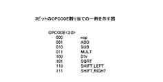
命令制御ユニット110は、命令の実行を制御する制御部であり、演算ユニット130に対して3ビットの信号OPCODEによって処理する演算を指示する。図3は、3ビットのOPCODE割り当ての一例を示す図である。同図に示すように、ここでは、"nop"から"SHIFT_RIGHT"までの8種類の演算を3ビットのOPCODEに割り当てている。
The
データ制御ユニット120は、演算ユニット130で演算されるデータに関する制御を行う制御部であり、演算ユニット130に演算データを出力する。
The
演算ユニット130は、データ制御ユニット120から受け取った演算データに対して命令制御ユニット110からOPCODEで指示された演算を実行する処理部であり、演算制御部131と、演算実行部132と、デバッグ機構133とを有する。
The
演算制御部131は、命令制御ユニット110からの制御信号により演算実行部132を制御する制御部である。演算実行部132は、データ制御ユニット120からの演算データに対して演算制御部131からの制御信号に従って演算を行う処理部である。
The
デバッグ機構133は、プロセッサ100のデバッグを支援する機能を提供する機構である。具体的には、このデバッグ機構133は、演算制御部131からOPCODEを入力してシフトレジスタ134にその値を記録する。図4は、デバッグ機構133の構成を示す機能ブロック図である。同図に示すように、このデバッグ機構133は、シフトレジスタ134とスキャン部135とを有する。
The
シフトレジスタ134は、OPCODEの過去6サイクル分の値を記憶するシフトレジスタである。すなわち、レジスタ"C0"は最新のOPCODEを記憶し、レジスタ"C1"は1クロック前のOPCODEを記憶し、レジスタ"C2"は2クロック前のOPCODEを記憶する。以下同様に、シフトレジスタ134は、5クロック前までのOPCODEの値を記憶する。 The shift register 134 is a shift register that stores values for the past six cycles of OPCODE. That is, the register “C0” stores the latest OPCODE, the register “C1” stores the OPCODE one clock before, and the register “C2” stores the OPCODE two clocks before. Similarly, the shift register 134 stores the value of OPCODE up to five clocks before.
今、図5に示すタイミングで命令制御ユニット110から演算ユニット130へOPCODEが送られていたとする。このときのデバッグ機構133内のシフトレジスタ134に保持されているOPCODEの値とそのタイミングは図6に示す通りである。図6に示すように、シフトレジスタ134には、"TIM 0"〜"TIM-5"までの過去6サイクル分のOPCODEが記録される。
Now, assume that OPCODE is sent from the
このように、シフトレジスタ134に過去6サイクル分のOPCODEの値を記録することによって、設計者は、過去6サイクルの間、SUB -> DIV -> MULT -> NOP -> DIV -> ADDの順序で命令制御ユニット110から演算制御信号が送られていたことを知ることができ、デバッグを効率良く行うことができる。
Thus, by recording the OPCODE values for the past 6 cycles in the shift register 134, the designer can change the order of SUB-> DIV-> MULT-> NOP-> DIV-> ADD during the last 6 cycles. Thus, it can be known that the arithmetic control signal has been sent from the
スキャン部135は、シフトレジスタ134に記憶された値をスキャンして読み出す処理部である。このスキャン部135がシフトレジスタ134に記憶された値をスキャンして読み出すことによって、設計者は、過去6サイクル分のOPCODEを知ることができる。
The
上述してきたように、本実施例1では、デバッグ機構133がシフトレジスタ134に過去6サイクル分のOPCODEを記憶し、スキャン部135がシフトレジスタ134に記憶されたOPCODEをスキャンして読み出すこととしたので、設計者は、OPCODEの時間的遷移を把握することができ、プロセッサのデバッグを効率良く行うことができる。
As described above, in the first embodiment, the
また、このような構成をとることにより、わずかな回路を追加するだけで、製造上の歩留まりや信頼性を低下させることなく、プロセッサ内回路の信号の時間的遷移を外部から知ることを可能とし、プロセッサのデバッグ作業の効率を向上させることができる。 In addition, by adopting such a configuration, it is possible to know the temporal transition of the signal in the circuit in the processor from outside without adding a few circuits and reducing the manufacturing yield and reliability. The efficiency of the processor debugging work can be improved.
なお、本実施例1では、シフトレジスタが6段構成である場合について説明したが、他の段数のシフトレジスタを使用することもできる。また、OPCODE以外の他の信号をシフトレジスタに記録することもできる。 In the first embodiment, the case where the shift register has a six-stage configuration has been described. However, shift registers having other stages can be used. Further, signals other than OPCODE can be recorded in the shift register.
ところで、上記実施例1では、過去6サイクル分のOPCODEを全てシフトレジスタ134に記録するプロセッサデバッグ装置について説明した。しかしながら、全てのサイクルのOPCODEではなく、特定のサイクルのOPCODEだけを知りたい場合もある。 By the way, in the first embodiment, the processor debug device that records all the OPCODEs for the past six cycles in the shift register 134 has been described. However, there are times when you want to know only the OPCODE of a specific cycle, not the OPCODE of every cycle.
例えば、図7は、信号Aとその有効性を示す信号Vを示す図である。同図において、信号Vの値が"1"である時のみ信号Aの値は有効であるとする。この場合、タイミング"TIM-2"、"TIM-4"、"TIM-6"および"TIM-7"での信号Aは無効であるため、デバッグ機構のシフトレジスタにこのタイミングの信号Aの値を記録しても意味を持たない。 For example, FIG. 7 is a diagram showing a signal A and a signal V indicating its effectiveness. In the figure, it is assumed that the value of the signal A is valid only when the value of the signal V is “1”. In this case, since the signal A at the timings “TIM-2”, “TIM-4”, “TIM-6”, and “TIM-7” is invalid, the value of the signal A at this timing is stored in the shift register of the debug mechanism. There is no point in recording.
従って、限られたデバック機構の資源を有効に使用するため、信号Vの値が"1"であるときにのみ信号Aの値を記録することが考えられる。そこで、本実施例2では、ある信号の値が"1"であるときにのみ特定の信号の値をシフトレジスタ記録するプロセッサデバッグ装置について説明する。 Therefore, in order to effectively use the resources of the limited debugging mechanism, it is conceivable to record the value of the signal A only when the value of the signal V is “1”. Therefore, in the second embodiment, a processor debug apparatus that records a value of a specific signal in a shift register only when the value of a certain signal is “1” will be described.
まず、本実施例2に係るプロセッサデバッグ装置による信号記録方式について図8−1〜図8−3を用いて説明する。図8−1は、信号Aの過去6サイクル分の情報を記録するシフトレジスタ("B10"〜"B15")を示す図である。 First, a signal recording method by the processor debug apparatus according to the second embodiment will be described with reference to FIGS. 8-1 to 8-3. FIG. 8A is a diagram illustrating shift registers (“B10” to “B15”) that record information for the past six cycles of the signal A. FIG.
ただし、このシフトレジスタ("B10"〜"B15")は、シフトレジスタ("B0"〜"B5")と異なり、信号Vが"1"であるときのみ信号Aを記録するように制御される。また、本実施例2に係るプロセッサデバッグ装置では、毎サイクルサイクリックにカウントする4ビットのカウンタを新たに設け、このカウンタ値も信号Aが記録される同じタイミングでシフトレジスタ("B20"〜"B25")に記録する。 However, unlike the shift registers ("B0" to "B5"), the shift registers ("B10" to "B15") are controlled to record the signal A only when the signal V is "1". . In addition, in the processor debug device according to the second embodiment, a 4-bit counter that counts cyclically every cycle is newly provided, and this counter value is also shifted to the shift register ("B20" to "B" at the same timing when the signal A is recorded. B25 ").
このように、信号Aが記録される同じタイミングでカウンタ値をシフトレジスタ("B20"〜"B25")に記録することによって、カウンタ値を用いて信号Aが記録されたタイミングを相対的に特定することができる。 Thus, by recording the counter value in the shift register ("B20" to "B25") at the same timing when the signal A is recorded, the timing at which the signal A is recorded is relatively specified using the counter value. can do.
図7に示した信号A、Vの状態の変化にカウンタの値を追記した例を図8−2に示す。このカウンタの値は信号A、Vのタイミングを相対的に示すものであり、今、"TIM 0"のタイミングで値がH'C'(16進数の'C')であったとする。このとき、デバッグ機構の各レジスタが記録している信号Aとカウンタの値、記録されているタイミングは図8−3に示す通りである。
An example in which the counter value is added to the change in the state of the signals A and V shown in FIG. 7 is shown in FIG. The value of this counter relatively indicates the timing of the signals A and V, and it is assumed that the value is now H'C '(hexadecimal' C ') at the timing of "
設計者は、シフトレジスタ("B10"〜"B15")に記録されている信号Aの値と、同じタイミングで記録されているシフトレジスタ("B20"〜"B25")のカウンタ値を調査することで、図8−2で示す信号Aの時間的遷移について知ることができる。また、設計者は、"TIM-9"から"TIM 0"までの10サイクル間の状態を知ることができるため、より効率良くデバッグを行うことができる。
The designer examines the value of the signal A recorded in the shift register ("B10" to "B15") and the counter value of the shift register ("B20" to "B25") recorded at the same timing. Thus, it is possible to know the temporal transition of the signal A shown in FIG. In addition, since the designer can know the state for 10 cycles from “TIM-9” to “
次に、本実施例2に係るプロセッサの構成について説明する。図9は、本実施例2に係るプロセッサの構成を示す機能ブロック図である。なお、ここでは説明の便宜上、図2に示した各部と同様の役割を果たす機能部については同一符号を付すこととしてその詳細な説明を省略する。 Next, the configuration of the processor according to the second embodiment will be described. FIG. 9 is a functional block diagram of the configuration of the processor according to the second embodiment. Here, for convenience of explanation, functional units that play the same functions as the respective units shown in FIG.
図9に示すように、このプロセッサ200は、命令制御ユニット210と、データ制御ユニット120と、演算ユニット230とを有する。命令制御ユニット210は、命令制御ユニット110と同様、命令の実行を制御する制御部であるが、演算ユニット230に対してOPCODEに加えてREQUEST_VALIDを出力する。ここで、REQUEST_VALIDは、OPCODEの有効性を示す信号であり、このREQUEST_VALIDが"1"のときのみOPCODEは有効となる。
As illustrated in FIG. 9, the processor 200 includes an
演算ユニット230は、演算ユニット130と同様、演算を実行する処理部であり、演算制御部231と、演算実行部232と、デバッグ機構233とを有する。演算制御部231は、命令制御ユニット210からOPCODEに加えてREQUEST_VALIDを制御信号として受け取り、演算実行部232を制御する制御部である。演算実行部232は、データ制御ユニット120からの演算データに対して演算制御部231からの制御信号に従って演算を行う処理部である。
Similar to the
デバッグ機構233は、プロセッサ200のデバッグを支援する機能を提供する機構であり、演算制御部231からOPCODEに加えてREQUEST_VALIDを入力し、REQUEST_VALIDが"1"のときのOPCODEをシフトレジスタ234に記録する。
The
図10は、デバッグ機構233の構成を示す機能ブロック図である。同図に示すように、このデバッグ機構233は、シフトレジスタ234および235と、カウンタ236と、スキャン部237とを有する。
FIG. 10 is a functional block diagram showing the configuration of the
シフトレジスタ234は、OPCODEとREQUEST_VALIDを入力し、REQUEST_VALIDが"1"のときのみOPCODEの値を記憶する。カウンタ236は、毎サイクルサイクリックにH'0'〜H'F'をカウントする4ビットのカウンタであり、OPCODEをシフトレジスタ234に記録したタイミングを特定するために使用される。
The
シフトレジスタ235は、REQUEST_VALIDが"1"のとき、すなわちOPCODEがシフトレジスタ234に記録されたタイミングでのカウンタ236の値を記憶する。スキャン部237は、シフトレジスタ234および235に記憶された値をスキャンして読み出す処理部である。
The
今、図11に示すタイミングで命令制御ユニット210から演算ユニット233へOPCODEおよびREQUEST_VALIDが送られていたとする。このときのデバッグ機構233内のシフトレジスタ234および235に保持されているOPCODEおよびカウンタの値とそのタイミングは図12に示す通りである。
Now, assume that OPCODE and REQUEST_VALID are sent from the
図12に示すように、シフトレジスタ234には、REQUEST_VALIDが"1"である"TIM 0"、"TIM-1"、"TIM-3"、"TIM-5"、"TIM-8"および"TIM-9"のOPCODEが記録され、シフトレジスタ235には、"TIM 0"、"TIM-1"、"TIM-3"、"TIM-5"、"TIM-8"および"TIM-9"のカウンタ値が記録される。
As shown in FIG. 12, the
従って、設計者は、デバッグ機構233のシフトレジスタ234とシフトレジスタ235に記録された値を調査することで、過去10サイクル中の6サイクルで、ADD -> SQRT -> SUB -> MULT -> DIV -> ADDの順序で命令制御ユニット210から有効な演算制御信号が送られ、演算実行部232で演算が行われていたことを知ることができ、さらに効率良くデバッグを行うことができる。
Therefore, the designer examines the values recorded in the
上述してきたように、本実施例2では、デバッグ機構233がOPCODEに加えてREQUEST_VALIDを入力し、REQUEST_VALIDが"1"であるときのみOPCODEの値をシフトレジスタ234に記憶することとしたので、シフトレジスタ234には有効な情報だけが記憶され、シフトレジスタ234を効率良く使用することができる。
As described above, in the second embodiment, the
実施例1および2では、一つのプロセッサ内に一つの演算ユニットがある場合について説明したが、スーパースカラ方式のプロセッサなどでは、一つのプロセッサ内に複数の演算ユニットがある。そこで、本実施例3では、一つのプロセッサ内に二つの演算ユニットがある場合について説明する。なお、ここでは、各演算ユニットごとに信号を記録するシフトレジスタを備えることとする。 In the first and second embodiments, the case where there is one arithmetic unit in one processor has been described. However, in a superscalar processor or the like, there are a plurality of arithmetic units in one processor. Thus, in the third embodiment, a case where there are two arithmetic units in one processor will be described. Here, it is assumed that each arithmetic unit includes a shift register that records a signal.
まず、本実施例3に係るプロセッサデバッグ装置による信号記録方式について図13−1〜図13−3を用いて説明する。今、図13−1に示すように、シフトレジスタXおよびYにおいて、それぞれ信号XA、YAをそれらが有効であるXV、YVが"1"であるときのみシフトレジスタ("B30"〜"B35")および("B50"〜"B55")へ記録させることとする。また、両シフトレジスタで共通のカウンタを設けその値もXA、YAが記録された同じタイミングでシフトレジスタ("B40"〜"B45")および("B60"〜"B65")へ記録するように制御する。 First, a signal recording method by the processor debug apparatus according to the third embodiment will be described with reference to FIGS. 13-1 to 13-3. Now, as shown in FIG. 13A, in the shift registers X and Y, the signals XA and YA are converted to the shift registers (“B30” to “B35” only when the XV and YV in which they are valid are “1”, respectively. ) And ("B50" to "B55"). In addition, a common counter is provided in both shift registers, and the values are recorded in the shift registers ("B40" to "B45") and ("B60" to "B65") at the same timing when XA and YA are recorded. Control.
例として、図13−2に示すように、信号X、Y、XVおよびYVが"TIM-9"から"TIM 0"での10クロックの間変化していたとし、"TIM 0"のタイミングでのカウンタ値がH'C'であったとする。この時の各シフトレジスタが記録している信号XA、YAとカウンタの値は図13−3の通りである。
As an example, as shown in FIG. 13-2, it is assumed that signals X, Y, XV and YV have changed for 10 clocks from “TIM-9” to “
このように、シフトレジスタ("B30"〜"B35")、("B40"〜"B45")、("B50"〜"B55")および("B60"〜"B65")に記録された値を調査することで、設計者は、図13−2での信号XA、YAの時間的遷移について、信号XAについては"TIM-9"から"TIM 0"までの10サイクル間の状態を知ることができ、信号YAについては"TIM-8"から"TIM 0"までの9サイクル間の状態を知ることができるとともに、両演算実行部での演算の同時実行状態も知ることができる。
Thus, the values recorded in the shift registers ("B30" to "B35"), ("B40" to "B45"), ("B50" to "B55") and ("B60" to "B65") By examining the above, the designer knows the state for 10 cycles from “TIM-9” to “
次に、本実施例3に係るプロセッサの構成について説明する。図14は、本実施例3に係るプロセッサの構成を示す機能ブロック図である。なお、ここでは説明の便宜上、図2に示した各部と同様の役割を果たす機能部については同一符号を付すこととしてその詳細な説明を省略する。 Next, the configuration of the processor according to the third embodiment will be described. FIG. 14 is a functional block diagram illustrating the configuration of the processor according to the third embodiment. Here, for convenience of explanation, functional units that play the same functions as the respective units shown in FIG.
図14に示すように、このプロセッサ300は、命令制御ユニット310と、データ制御ユニット320と、演算ユニットX330と、演算ユニットY340と、デバッグ機構350とを有する。
As illustrated in FIG. 14, the processor 300 includes an instruction control unit 310, a data control unit 320, an
命令制御ユニット310は、命令の実行を制御する制御部であり、演算ユニットX330に対してOPCODE_XおよびREQUEST_VALID_Xを出力し、演算ユニットY340に対してOPCODE_YおよびREQUEST_VALID_Yを出力する。 The instruction control unit 310 is a control unit that controls the execution of instructions, and outputs OPCODE_X and REQUEST_VALID_X to the arithmetic unit X330, and outputs OPCODE_Y and REQUEST_VALID_Y to the arithmetic unit Y340.
ここで、OPCODE_XおよびOPCODE_Yは、演算を指示する3ビットの信号であり、その割り当ては、図3に示した3ビットのOPCODEの割り当てと同じである。また、REQUEST_VALID_Xは、OPCODE_Xの有効性を示す信号であり、このREQUEST_VALID_Xが"1"のときのみOPCODE_Xは有効となり、REQUEST_VALID_Yは、OPCODE_Yの有効性を示す信号であり、このREQUEST_VALID_Yが"1"のときのみOPCODE_Yは有効となる。 Here, OPCODE_X and OPCODE_Y are 3-bit signals for instructing operations, and the assignment is the same as the assignment of the 3-bit OPCODE shown in FIG. REQUEST_VALID_X is a signal indicating the validity of OPCODE_X. OPCODE_X is valid only when this REQUEST_VALID_X is "1", and REQUEST_VALID_Y is a signal indicating the validity of OPCODE_Y. When this REQUEST_VALID_Y is "1" Only OPCODE_Y is valid.
データ制御ユニット320は、演算ユニットX330および演算ユニットY340で演算されるデータに関する制御を行う制御部であり、演算ユニットX330および演算ユニットY340に演算データを出力する。 The data control unit 320 is a control unit that controls the data calculated by the arithmetic unit X330 and the arithmetic unit Y340, and outputs arithmetic data to the arithmetic unit X330 and the arithmetic unit Y340.
演算ユニットX330は、データ制御ユニット320から受け取った演算データに対して命令制御ユニット310から指示された演算を実行する処理部であり、演算制御部331と、演算実行部332とを有する。
The arithmetic unit X330 is a processing unit that performs an operation instructed by the instruction control unit 310 on the arithmetic data received from the data control unit 320, and includes an
演算制御部331は、命令制御ユニット310からOPCODE_XおよびREQUEST_VALID_Xを受け取り、演算実行部332を制御する制御部である。演算実行部332は、データ制御ユニット320からの演算データに対して演算制御部331からの制御信号に従って演算を行う処理部である。なお、演算ユニットY340も、演算ユニットX330と同様の機能構成を有する。
The
デバッグ機構350は、プロセッサ300のデバッグを支援する機能を提供する機構であり、演算制御部331からOPCODE_XおよびREQUEST_VALID_Xを入力し、REQUEST_VALID_Xが"1"であるときのみOPCODE_Xの値をシフトレジスタ351に記録し、演算制御部341からOPCODE_YおよびREQUEST_VALID_Yを入力し、REQUEST_VALID_Yが"1"であるときのみOPCODE_Yの値をシフトレジスタ353に記録する。
The
図15は、デバッグ機構350の構成を示す機能ブロック図である。同図に示すように、このデバッグ機構350は、シフトレジスタ351〜354と、カウンタ355と、スキャン部356とを有する。
FIG. 15 is a functional block diagram showing the configuration of the
シフトレジスタ351は、OPCODE_XとREQUEST_VALID_Xを入力し、REQUEST_VALID_Xが"1"のときのみOPCODE_Xの値を記憶する。シフトレジスタ353は、OPCODE_YとREQUEST_VALID_Yを入力し、REQUEST_VALID_Yが"1"のときのみOPCODE_Yの値を記憶する。
The
カウンタ355は、毎サイクルサイクリックにカウントH'0'〜H'F'をカウントする4ビットのカウンタであり、OPCODE_XまたはOPCODE_Yを記録したタイミングを特定するために使用される。
The
シフトレジスタ352は、REQUEST_VALID_Xが"1"のとき、すなわちOPCODE_Xがシフトレジスタ351に記録されたタイミングでのカウンタ355の値を記憶する。シフトレジスタ354は、REQUEST_VALID_Yが"1"のとき、すなわちOPCODE_Yがシフトレジスタ353に記録されたタイミングでのカウンタ355の値を記憶する。スキャン部356は、シフトレジスタ351〜354に記憶された値をスキャンして読み出す処理部である。
The
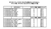
今、図16に示すタイミングで命令制御ユニット310から、演算ユニットX330へOPCODE_XおよびREQUEST_VALID_Xが送られ、演算ユニットY340へOPCODE_YおよびREQUEST_VALID_Yが送られていたとする。このときのデバッグ機構350内のシフトレジスタ351および352に保持されているOPCODE_Xおよびカウンタの値と、シフトレジスタ353および354に保持されているOPCODE_Yおよびカウンタの値と、それらのタイミングは図17に示す通りである。
Now, assume that OPCODE_X and REQUEST_VALID_X are sent from the instruction control unit 310 to the arithmetic unit X330 and OPCODE_Y and REQUEST_VALID_Y are sent to the arithmetic unit Y340 at the timing shown in FIG. The OPCODE_X and counter values held in the shift registers 351 and 352 in the
図17に示すように、シフトレジスタ351には、REQUEST_VALID_Xが"1"である"TIM 0"、"TIM-1"、"TIM-3"、"TIM-5"、"TIM-8"および"TIM-9"のOPCODE_Xが記録され、シフトレジスタ352には、"TIM 0"、"TIM-1"、"TIM-3"、"TIM-5"、"TIM-8"および"TIM-9"のカウンタ値が記録される。また、シフトレジスタ353には、REQUEST_VALID_Yが"1"である"TIM 0"、"TIM-2"、"TIM-4"、"TIM-5"、"TIM-6"および"TIM-8"のOPCODE_Yが記録され、シフトレジスタ354には、"TIM 0"、"TIM-2"、"TIM-4"、"TIM-5"、"TIM-6"および"TIM-8"のカウンタ値が記録される。
As shown in FIG. 17, the
従って、設計者は、デバッグ機構350のシフトレジスタ351および352の値を調査することで、演算ユニットX330において過去10サイクルの間、ADD -> SQRT -> SUB -> MULT -> DIV -> ADDの順序で命令制御ユニット310から有効なOPCODE_Xが送られ、演算実行部332で演算が行われていたことを知ることができ、シフトレジスタ353および354の値を調査することで、演算ユニットY340において過去9サイクルの間、ADD -> MULT -> SHIFT_LEFT -> ADD -> MLT -> SHIFT_LEFTの順序で命令制御ユニット310から有効なOPCODE_Yが送られ、演算実行部342で演算が行われていたことを知ることができる。
Therefore, the designer examines the values of the shift registers 351 and 352 of the
また、シフトレジスタ352および354で記録しているカウンタ値は演算ユニットX330および演算ユニットY340で共通なものであるため、設計者は、これらに記録されている値より両演算ユニットで処理した演算のタイミングを知ることができ、デバッグの効率をさらに向上することができる。例えば、設計者は、"TIM 0"、"TIM-5"および"TIM-8"においては演算ユニットX330と演算ユニットY340が同時に演算を行っていたことを知ることができる。
Further, since the counter values recorded in the shift registers 352 and 354 are common to the arithmetic unit X330 and the arithmetic unit Y340, the designer can calculate the arithmetic values processed by both arithmetic units from the values recorded in these counters. The timing can be known, and the debugging efficiency can be further improved. For example, the designer can know that in “
上述してきたように、本実施例3では、デバッグ機構350が二つの演算ユニットで行われていた演算を記録し、両演算ユニットで処理された演算のタイミングを設計者が知ることを可能としたので、デバッグの効率をさらに向上することができる。
As described above, in the third embodiment, the
なお、本実施例3では、プロセッサが二つの演算ユニットを有する場合について説明したが、デバッグ機構内のシフトレジスタの個数を増やすことによって、より多くの演算ユニットを有するプロセッサを対象とすることもできる。 In the third embodiment, the case where the processor has two arithmetic units has been described. However, by increasing the number of shift registers in the debugging mechanism, a processor having more arithmetic units can be targeted. .
実施例1〜3では、プロセッサ内の決められた信号の時間的遷移を調査する場合について説明したが、プロセッサ内の複数の信号のうちいずれかの信号を選択してその時間的遷移を調査したい場合もある。そこで、本実施例4では、プロセッサ内の二つの信号のうちいずれかの信号を選択してシフトレジスタに記録する場合について説明する。 In the first to third embodiments, the case of investigating the temporal transition of a predetermined signal in the processor has been described. However, one of a plurality of signals in the processor is selected to investigate the temporal transition. In some cases. Thus, in the fourth embodiment, a case will be described in which one of the two signals in the processor is selected and recorded in the shift register.
図18は、本実施例4に係るプロセッサの構成を示す機能ブロック図である。なお、ここでは説明の便宜上、図2に示した各部と同様の役割を果たす機能部については同一符号を付すこととしてその詳細な説明を省略する。 FIG. 18 is a functional block diagram of the configuration of the processor according to the fourth embodiment. Here, for convenience of explanation, functional units that play the same functions as the respective units shown in FIG.
同図に示すように、このプロセッサ400の演算ユニット430は、演算制御部131と、演算実行部432と、デバッグ機構433とを有する。
As shown in the figure, the
演算実行部432は、演算制御部131からの制御信号に従って演算を行う処理部であり、デバッグ機構433に対してRUPT_CODEを出力する。ここで、RUPT_CODEは、演算結果の状態を示す3ビットの信号である。
The
デバッグ機構433は、プロセッサ400のデバッグを支援する機能を提供する機構であり、選択信号に基づいてOPCODEまたはRUPT_CODEのいずれかをシフトレジスタに記録する。ここで、選択信号は、スキャン可能なラッチの出力であり、プロセッサ400の外部から設定可能である。
The
図19は、デバッグ機構433の構成を示す機能ブロック図である。同図に示すように、このデバッグ機構433は、シフトレジスタ434と、セレクタ440と、スキャン部135とを有する。
FIG. 19 is a functional block diagram showing the configuration of the
シフトレジスタ434は、OPCODEまたはRUPT_CODEの過去6サイクル分の値を記憶するシフトレジスタである。セレクタ440は、OPCODE、RUPT_CODEおよび選択信号を入力し、選択信号に基づいてOPCODEまたはRUPT_CODEを選択し、シフトレジスタ434に出力する処理部である。すなわち、シフトレジスタ434は、セレクタ440によって選択されたOPCODEまたはRUPT_CODE の過去6サイクル分の値を記憶する。
The
上述してきたように、本実施例4では、セレクタ440がOPCODEまたはRUPT_CODEを選択し、シフトレジスタ434がセレクタ440によって選択されたOPCODEまたはRUPT_CODEの過去6サイクル分の値を記憶することとしたので、記録可能な信号の種類をわずかなハードウェアの増加で増やすことができる。
As described above, in the fourth embodiment, the
なお、本実施例4では、REQUEST_VALIDを使用しない場合について説明したが、REQUEST_VALIDを使用し、REQUEST_VALIDの値が"1"であるときのみOPCODEまたはRUPT_CODEをシフトレジスタに記録することもできる。 In the fourth embodiment, REQUEST_VALID is not used. However, REQUEST_VALID is used, and OPCODE or RUPT_CODE can be recorded in the shift register only when the value of REQUEST_VALID is “1”.
また、本実施例1〜4に係るデバッグ機構に記録させる信号数とクロック数、カウンタのビット幅は設計者がプロセッサ内に搭載できる回路量とその必要性から任意に決定できるため、このデバッグ機構の回路規模は、RAMで構成されたものが1K、2Kビットなどある単位でしか実装できないのに比べ、設計者が必要な最低限で実現することができる。 Further, since the number of signals and the number of clocks to be recorded in the debugging mechanism according to the first to fourth embodiments and the bit width of the counter can be arbitrarily determined by the designer from the amount of circuit that can be installed in the processor and the necessity thereof, this debugging mechanism The circuit scale can be realized at the minimum required by the designer, compared with the case where the RAM is implemented only in a certain unit such as 1K or 2K bits.
(付記1)プロセッサ内のラッチをスキャンして読み出すプロセッサデバッグ装置であって、
プロセッサ内の所定の信号の値を複数のクロック分記憶するレジスタと、
前記レジスタにより記憶された信号値をスキャンして読み出す信号読出手段と、
を備えたことを特徴とするプロセッサデバッグ装置。
(Appendix 1) A processor debug device that scans and reads a latch in a processor,
A register for storing a value of a predetermined signal in the processor for a plurality of clocks;
Signal reading means for scanning and reading the signal value stored by the register;
A processor debug device comprising:
(付記2)前記レジスタに信号値を記憶するタイミングを指定するタイミング指定手段と、
前記タイミング指定手段により指定されたタイミングを識別するタイミング値を前記レジスタにより記憶される複数の信号のそれぞれに対応して記憶するタイミング記憶手段と、
をさらに備えたことを特徴とする付記1に記載のプロセッサデバッグ装置。
(Supplementary Note 2) Timing designation means for designating timing for storing a signal value in the register;
Timing storage means for storing a timing value for identifying the timing designated by the timing designation means corresponding to each of a plurality of signals stored by the register;
The processor debug device according to
(付記3)プロセッサ内の複数の信号から一つの信号を選択する信号選択手段をさらに備え、
前記レジスタは、前記信号選択手段により選択された信号の値を複数のクロック分記憶することを特徴とする付記1または2に記載のプロセッサデバッグ装置。
(Supplementary note 3) Further comprising signal selection means for selecting one signal from a plurality of signals in the processor,
3. The processor debug apparatus according to
(付記4)前記レジスタは、シフトレジスタであることを特徴とする付記1または2に記載のプロセッサデバッグ装置。
(Supplementary note 4) The processor debug device according to
(付記5)前記タイミング記憶手段により記憶されるタイミング値は、カウンタによりカウントされるカウント値であることを特徴とする付記2に記載のプロセッサデバッグ装置。
(Supplementary note 5) The processor debug device according to
(付記6)プロセッサ内のラッチをスキャンして読み出すプロセッサデバッグ方法であって、
プロセッサ内の所定の信号の値が複数のクロック分レジスタに保持されるように記録する信号記録工程と、
前記信号記録工程によりレジスタに記録された信号値をスキャンして読み出す信号読出工程と、
を含んだことを特徴とするプロセッサデバッグ方法。
(Appendix 6) A processor debugging method for scanning and reading a latch in a processor,
A signal recording step of recording so that a value of a predetermined signal in the processor is held in a register for a plurality of clocks;
A signal readout step of scanning and reading out the signal value recorded in the register by the signal recording step;
A processor debugging method comprising:
(付記7)前記信号記録工程は、指定されたタイミングでレジスタに信号値を記録し、
前記タイミングを識別するタイミング値を前記レジスタにより記録される複数の信号のそれぞれに対応して記録するタイミング記録工程、
をさらに含んだことを特徴とする付記6に記載のプロセッサデバッグ方法。
(Appendix 7) The signal recording step records a signal value in a register at a designated timing,
A timing recording step of recording a timing value for identifying the timing corresponding to each of a plurality of signals recorded by the register;
The processor debug method according to
(付記8)プロセッサ内の複数の信号から一つの信号を選択する信号選択工程をさらに含み、
前記信号記録工程は、前記信号選択工程により選択された信号の値を複数のクロック分レジスタに記録することを特徴とする付記6または7に記載のプロセッサデバッグ方法。
(Additional remark 8) It further includes the signal selection process which selects one signal from the several signal in a processor,
The processor debug method according to
(付記9)前記レジスタは、シフトレジスタであることを特徴とする付記6または7に記載のプロセッサデバッグ方法。
(Supplementary note 9) The processor debugging method according to
(付記10)前記タイミング記録工程により記録されるタイミング値は、カウンタによりカウントされるカウント値であることを特徴とする付記7に記載のプロセッサデバッグ方法。
(Supplementary note 10) The processor debugging method according to
以上のように、本発明に係るプロセッサデバッグ装置およびプロセッサデバッグ方法は、プロセッサの試験に有用であり、特に、信号の値の前後関係で発生するタイミング障害の解析などに適している。 As described above, the processor debug device and the processor debug method according to the present invention are useful for processor testing, and are particularly suitable for analysis of timing faults occurring in the context of signal values.
100,200,300,400 プロセッサ
110,210,310 命令制御ユニット
120,320 データ制御ユニット
130,230,430 演算ユニット
131,231,331,341 演算制御部
132,232,332,342,432 演算実行部
133,233,350,433 デバッグ機構
134,234,351,353,434 シフトレジスタ
135,237,356 スキャン部
235,352,354 シフトレジスタ
236,355 カウンタ
330 演算ユニットX
340 演算ユニットY
100, 200, 300, 400
340 arithmetic unit Y
Claims (4)
プロセッサ内に設けられ、該プロセッサ内の所定の信号の値を複数のクロック分記憶するシフトレジスタと、
前記シフトレジスタにより記憶された信号値をスキャンして読み出す信号読出手段と、 を備えたことを特徴とするプロセッサデバッグ装置。 A processor debug device that scans and reads a shift register in a processor,
A shift register provided in the processor and storing a value of a predetermined signal in the processor for a plurality of clocks;
And a signal reading unit that scans and reads out the signal value stored by the shift register.
前記タイミング指定手段により指定されたタイミングを識別するタイミング値を前記シフトレジスタにより記憶される複数の信号のそれぞれに対応して記憶するタイミング記憶手段と、
をさらに備えたことを特徴とする請求項1に記載のプロセッサデバッグ装置。 Timing designating means for designating timing for storing a signal value in the shift register;
Timing storage means for storing a timing value for identifying the timing designated by the timing designation means corresponding to each of a plurality of signals stored by the shift register;
The processor debug device according to claim 1, further comprising:
前記シフトレジスタは、前記信号選択手段により選択された信号の値を複数のクロック分記憶することを特徴とする請求項1または2に記載のプロセッサデバッグ装置。 Signal selection means for selecting one signal from a plurality of signals in the processor;
3. The processor debug apparatus according to claim 1, wherein the shift register stores a value of a signal selected by the signal selection unit for a plurality of clocks.
プロセッサ内に設けられたシフトレジスタに、該プロセッサ内の所定の信号の値が複数
のクロック分保持されるように記録する信号記録工程と、
前記信号記録工程によりシフトレジスタに記録された信号値をスキャンして読み出す信
号読出工程と、
を含んだことを特徴とするプロセッサデバッグ方法。 A processor debug method for scanning and reading a shift register in a processor,
A signal recording step of recording in a shift register provided in the processor so that a value of a predetermined signal in the processor is held for a plurality of clocks;
A signal reading step of scanning and reading the signal value recorded in the shift register by the signal recording step;
A processor debugging method comprising:
Priority Applications (2)
| Application Number | Priority Date | Filing Date | Title |
|---|---|---|---|
| JP2004222398A JP4494899B2 (en) | 2004-07-29 | 2004-07-29 | Processor debugging apparatus and processor debugging method |
| US10/986,912 US8015447B2 (en) | 2004-07-29 | 2004-11-15 | Processor debugging apparatus and processor debugging method |
Applications Claiming Priority (1)
| Application Number | Priority Date | Filing Date | Title |
|---|---|---|---|
| JP2004222398A JP4494899B2 (en) | 2004-07-29 | 2004-07-29 | Processor debugging apparatus and processor debugging method |
Related Child Applications (1)
| Application Number | Title | Priority Date | Filing Date |
|---|---|---|---|
| JP2009220855A Division JP5177108B2 (en) | 2009-09-25 | 2009-09-25 | Arithmetic processing device and control method of arithmetic processing device |
Publications (2)
| Publication Number | Publication Date |
|---|---|
| JP2006040172A JP2006040172A (en) | 2006-02-09 |
| JP4494899B2 true JP4494899B2 (en) | 2010-06-30 |
Family
ID=35733799
Family Applications (1)
| Application Number | Title | Priority Date | Filing Date |
|---|---|---|---|
| JP2004222398A Expired - Fee Related JP4494899B2 (en) | 2004-07-29 | 2004-07-29 | Processor debugging apparatus and processor debugging method |
Country Status (2)
| Country | Link |
|---|---|
| US (1) | US8015447B2 (en) |
| JP (1) | JP4494899B2 (en) |
Families Citing this family (3)
| Publication number | Priority date | Publication date | Assignee | Title |
|---|---|---|---|---|
| WO2007097039A1 (en) * | 2006-02-27 | 2007-08-30 | Fujitsu Limited | Processor debug mechanism |
| US20180288889A1 (en) * | 2017-03-30 | 2018-10-04 | Google Inc. | Circuit board and battery architecture of an electronic device |
| US10789153B2 (en) * | 2018-04-03 | 2020-09-29 | Xilinx, Inc. | Debug controller circuit |
Citations (1)
| Publication number | Priority date | Publication date | Assignee | Title |
|---|---|---|---|---|
| JP2002149442A (en) * | 2000-11-10 | 2002-05-24 | Hitachi Ltd | Data processor |
Family Cites Families (19)
| Publication number | Priority date | Publication date | Assignee | Title |
|---|---|---|---|---|
| JPS52130246A (en) * | 1976-04-24 | 1977-11-01 | Fujitsu Ltd | Memory access control system |
| JPS58169643A (en) | 1982-03-31 | 1983-10-06 | Fujitsu Ltd | Diagnosing circuit of information processor |
| JPS60159951A (en) * | 1984-01-30 | 1985-08-21 | Fuji Electric Co Ltd | Tracing system in information processing device |
| US4720778A (en) * | 1985-01-31 | 1988-01-19 | Hewlett Packard Company | Software debugging analyzer |
| GB2220272B (en) * | 1988-06-29 | 1992-09-30 | Texas Instruments Ltd | Improvements in or relating to integrated circuits |
| JPH03204737A (en) * | 1990-01-08 | 1991-09-06 | Nec Corp | Debug circuit of signal processing processor |
| US5253255A (en) * | 1990-11-02 | 1993-10-12 | Intel Corporation | Scan mechanism for monitoring the state of internal signals of a VLSI microprocessor chip |
| JPH05242272A (en) | 1992-01-28 | 1993-09-21 | Nec Corp | Microprocessor |
| GB9217728D0 (en) | 1992-08-20 | 1992-09-30 | Texas Instruments Ltd | Method of testing interconnections between integrated circuits in a circuit |
| JPH07182305A (en) | 1993-12-24 | 1995-07-21 | Kawasaki Steel Corp | Microprocessor |
| JPH08171505A (en) * | 1994-12-16 | 1996-07-02 | Fujitsu Ltd | Semiconductor device |
| JP2752592B2 (en) * | 1994-12-28 | 1998-05-18 | 日本ヒューレット・パッカード株式会社 | Microprocessor, signal transmission method between microprocessor and debug tool, and tracing method |
| US6154856A (en) * | 1997-04-08 | 2000-11-28 | Advanced Micro Devices, Inc. | Debug interface including state machines for timing synchronization and communication |
| JP4335999B2 (en) * | 1999-05-20 | 2009-09-30 | 株式会社ルネサステクノロジ | Semiconductor integrated circuit device with built-in processor |
| US6859891B2 (en) * | 1999-10-01 | 2005-02-22 | Stmicroelectronics Limited | Apparatus and method for shadowing processor information |
| US6463553B1 (en) * | 1999-10-01 | 2002-10-08 | Stmicroelectronics, Ltd. | Microcomputer debug architecture and method |
| US6550031B1 (en) * | 1999-10-06 | 2003-04-15 | Advanced Micro Devices Inc. | Transparently gathering a chips multiple internal states via scan path and a trigger |
| US7168032B2 (en) * | 2000-12-15 | 2007-01-23 | Intel Corporation | Data synchronization for a test access port |
| US7650539B2 (en) * | 2005-06-30 | 2010-01-19 | Microsoft Corporation | Observing debug counter values during system operation |
-
2004
- 2004-07-29 JP JP2004222398A patent/JP4494899B2/en not_active Expired - Fee Related
- 2004-11-15 US US10/986,912 patent/US8015447B2/en not_active Expired - Fee Related
Patent Citations (1)
| Publication number | Priority date | Publication date | Assignee | Title |
|---|---|---|---|---|
| JP2002149442A (en) * | 2000-11-10 | 2002-05-24 | Hitachi Ltd | Data processor |
Also Published As
| Publication number | Publication date |
|---|---|
| US20060026470A1 (en) | 2006-02-02 |
| JP2006040172A (en) | 2006-02-09 |
| US8015447B2 (en) | 2011-09-06 |
Similar Documents
| Publication | Publication Date | Title |
|---|---|---|
| US7870438B2 (en) | Method, system and computer program product for sampling computer system performance data | |
| US6961872B2 (en) | Microcomputer and debugging system | |
| JP4171016B2 (en) | Method for circuit testing using LBIST | |
| JP3893238B2 (en) | Semiconductor memory device failure analysis device | |
| US20020176288A1 (en) | Semiconductor integrated circuit device and test method thereof | |
| US7536615B1 (en) | Logic analyzer systems and methods for programmable logic devices | |
| US9015543B2 (en) | Diagnosis-aware scan chain stitching | |
| US7260759B1 (en) | Method and apparatus for an efficient memory built-in self test architecture for high performance microprocessors | |
| KR20200088760A (en) | Checksum generation | |
| JP4494899B2 (en) | Processor debugging apparatus and processor debugging method | |
| US20040054950A1 (en) | Apparatus and method for device selective scans in data streaming test environment for a processing unit having multiple cores | |
| US7617428B2 (en) | Circuits and associated methods for improved debug and test of an application integrated circuit | |
| JP5177108B2 (en) | Arithmetic processing device and control method of arithmetic processing device | |
| Silveira et al. | Flexible architecture of memory BISTs | |
| US7624323B2 (en) | Method and apparatus for testing an IC device based on relative timing of test signals | |
| JP2007058450A (en) | Semiconductor integrated circuit | |
| US10796043B1 (en) | Non-adaptive pattern reordering to improve scan chain diagnostic resolution in circuit design and manufacture | |
| Park et al. | Post-silicon bug localization for processors using IFRA | |
| Grosso et al. | A software-based self-test methodology for system peripherals | |
| US7222202B2 (en) | Method for monitoring a set of semaphore registers using a limited-width test bus | |
| JP2002288005A (en) | Trace data extracting method for debug and performance analysis | |
| JP4526985B2 (en) | Test system | |
| US11892508B2 (en) | Joint test action group transmission system capable of transmitting data continuously | |
| JPS62164140A (en) | Testing of data processing system | |
| TW201913389A (en) | Semiconductor device |
Legal Events
| Date | Code | Title | Description |
|---|---|---|---|
| A621 | Written request for application examination |
Free format text: JAPANESE INTERMEDIATE CODE: A621 Effective date: 20061027 |
|
| A977 | Report on retrieval |
Free format text: JAPANESE INTERMEDIATE CODE: A971007 Effective date: 20080227 |
|
| A131 | Notification of reasons for refusal |
Free format text: JAPANESE INTERMEDIATE CODE: A131 Effective date: 20080304 |
|
| A521 | Written amendment |
Free format text: JAPANESE INTERMEDIATE CODE: A523 Effective date: 20080507 |
|
| A02 | Decision of refusal |
Free format text: JAPANESE INTERMEDIATE CODE: A02 Effective date: 20090630 |
|
| A521 | Written amendment |
Free format text: JAPANESE INTERMEDIATE CODE: A523 Effective date: 20090925 |
|
| A911 | Transfer to examiner for re-examination before appeal (zenchi) |
Free format text: JAPANESE INTERMEDIATE CODE: A911 Effective date: 20091006 |
|
| A131 | Notification of reasons for refusal |
Free format text: JAPANESE INTERMEDIATE CODE: A131 Effective date: 20100112 |
|
| A521 | Written amendment |
Free format text: JAPANESE INTERMEDIATE CODE: A523 Effective date: 20100311 |
|
| TRDD | Decision of grant or rejection written | ||
| A01 | Written decision to grant a patent or to grant a registration (utility model) |
Free format text: JAPANESE INTERMEDIATE CODE: A01 Effective date: 20100406 |
|
| A01 | Written decision to grant a patent or to grant a registration (utility model) |
Free format text: JAPANESE INTERMEDIATE CODE: A01 |
|
| A61 | First payment of annual fees (during grant procedure) |
Free format text: JAPANESE INTERMEDIATE CODE: A61 Effective date: 20100408 |
|
| R150 | Certificate of patent or registration of utility model |
Free format text: JAPANESE INTERMEDIATE CODE: R150 |
|
| FPAY | Renewal fee payment (event date is renewal date of database) |
Free format text: PAYMENT UNTIL: 20130416 Year of fee payment: 3 |
|
| FPAY | Renewal fee payment (event date is renewal date of database) |
Free format text: PAYMENT UNTIL: 20140416 Year of fee payment: 4 |
|
| LAPS | Cancellation because of no payment of annual fees |