JP4493779B2 - Semiconductor device and manufacturing method thereof - Google Patents
Semiconductor device and manufacturing method thereof Download PDFInfo
- Publication number
- JP4493779B2 JP4493779B2 JP2000022022A JP2000022022A JP4493779B2 JP 4493779 B2 JP4493779 B2 JP 4493779B2 JP 2000022022 A JP2000022022 A JP 2000022022A JP 2000022022 A JP2000022022 A JP 2000022022A JP 4493779 B2 JP4493779 B2 JP 4493779B2
- Authority
- JP
- Japan
- Prior art keywords
- film
- contact
- silicon
- atomic
- silicon oxynitride
- Prior art date
- Legal status (The legal status is an assumption and is not a legal conclusion. Google has not performed a legal analysis and makes no representation as to the accuracy of the status listed.)
- Expired - Fee Related
Links
- 239000004065 semiconductor Substances 0.000 title claims description 107
- 238000004519 manufacturing process Methods 0.000 title claims description 32
- 239000010408 film Substances 0.000 claims description 378
- XUIMIQQOPSSXEZ-UHFFFAOYSA-N Silicon Chemical compound [Si] XUIMIQQOPSSXEZ-UHFFFAOYSA-N 0.000 claims description 128
- 229910052710 silicon Inorganic materials 0.000 claims description 128
- 239000010703 silicon Substances 0.000 claims description 128
- 239000000758 substrate Substances 0.000 claims description 103
- IJGRMHOSHXDMSA-UHFFFAOYSA-N Atomic nitrogen Chemical compound N#N IJGRMHOSHXDMSA-UHFFFAOYSA-N 0.000 claims description 76
- 238000000034 method Methods 0.000 claims description 67
- 229910052739 hydrogen Inorganic materials 0.000 claims description 62
- 229910052760 oxygen Inorganic materials 0.000 claims description 51
- 239000000203 mixture Substances 0.000 claims description 48
- 239000001257 hydrogen Substances 0.000 claims description 44
- 229910052757 nitrogen Inorganic materials 0.000 claims description 38
- UFHFLCQGNIYNRP-UHFFFAOYSA-N Hydrogen Chemical compound [H][H] UFHFLCQGNIYNRP-UHFFFAOYSA-N 0.000 claims description 37
- QVGXLLKOCUKJST-UHFFFAOYSA-N atomic oxygen Chemical compound [O] QVGXLLKOCUKJST-UHFFFAOYSA-N 0.000 claims description 32
- 239000001301 oxygen Substances 0.000 claims description 32
- 239000007789 gas Substances 0.000 claims description 19
- 238000005268 plasma chemical vapour deposition Methods 0.000 claims description 13
- 238000000151 deposition Methods 0.000 claims description 11
- 230000008021 deposition Effects 0.000 claims description 11
- 239000010409 thin film Substances 0.000 claims description 9
- 230000001965 increasing effect Effects 0.000 claims description 8
- 238000009751 slip forming Methods 0.000 claims description 8
- 230000007423 decrease Effects 0.000 claims description 5
- 239000010410 layer Substances 0.000 description 71
- 239000012535 impurity Substances 0.000 description 40
- 239000002585 base Substances 0.000 description 38
- 230000015572 biosynthetic process Effects 0.000 description 20
- 229910021419 crystalline silicon Inorganic materials 0.000 description 20
- PXHVJJICTQNCMI-UHFFFAOYSA-N Nickel Chemical compound [Ni] PXHVJJICTQNCMI-UHFFFAOYSA-N 0.000 description 17
- 229910021417 amorphous silicon Inorganic materials 0.000 description 17
- 239000004973 liquid crystal related substance Substances 0.000 description 17
- 239000011159 matrix material Substances 0.000 description 17
- 230000008569 process Effects 0.000 description 17
- 238000006243 chemical reaction Methods 0.000 description 16
- OAICVXFJPJFONN-UHFFFAOYSA-N Phosphorus Chemical compound [P] OAICVXFJPJFONN-UHFFFAOYSA-N 0.000 description 15
- 239000011521 glass Substances 0.000 description 15
- 229910052698 phosphorus Inorganic materials 0.000 description 15
- 239000011574 phosphorus Substances 0.000 description 15
- VYPSYNLAJGMNEJ-UHFFFAOYSA-N silicon dioxide Inorganic materials O=[Si]=O VYPSYNLAJGMNEJ-UHFFFAOYSA-N 0.000 description 15
- 229910052814 silicon oxide Inorganic materials 0.000 description 14
- 238000002425 crystallisation Methods 0.000 description 13
- 238000010586 diagram Methods 0.000 description 13
- 238000010438 heat treatment Methods 0.000 description 13
- 230000003287 optical effect Effects 0.000 description 13
- 229910052581 Si3N4 Inorganic materials 0.000 description 12
- 230000008025 crystallization Effects 0.000 description 12
- 239000011229 interlayer Substances 0.000 description 12
- HQVNEWCFYHHQES-UHFFFAOYSA-N silicon nitride Chemical compound N12[Si]34N5[Si]62N3[Si]51N64 HQVNEWCFYHHQES-UHFFFAOYSA-N 0.000 description 12
- 125000004429 atom Chemical group 0.000 description 10
- 150000002500 ions Chemical class 0.000 description 9
- 230000000903 blocking effect Effects 0.000 description 8
- 230000003197 catalytic effect Effects 0.000 description 8
- 229910052759 nickel Inorganic materials 0.000 description 8
- 238000000137 annealing Methods 0.000 description 7
- 230000010355 oscillation Effects 0.000 description 7
- 230000009471 action Effects 0.000 description 6
- 230000008901 benefit Effects 0.000 description 6
- 230000008859 change Effects 0.000 description 6
- 238000005224 laser annealing Methods 0.000 description 6
- 239000003990 capacitor Substances 0.000 description 5
- 230000001976 improved effect Effects 0.000 description 5
- 229920001721 polyimide Polymers 0.000 description 5
- 239000011347 resin Substances 0.000 description 5
- 229920005989 resin Polymers 0.000 description 5
- XYFCBTPGUUZFHI-UHFFFAOYSA-N Phosphine Chemical compound P XYFCBTPGUUZFHI-UHFFFAOYSA-N 0.000 description 4
- 239000004642 Polyimide Substances 0.000 description 4
- 238000004140 cleaning Methods 0.000 description 4
- 230000000694 effects Effects 0.000 description 4
- 238000005530 etching Methods 0.000 description 4
- 150000002431 hydrogen Chemical class 0.000 description 4
- 238000005984 hydrogenation reaction Methods 0.000 description 4
- 238000002161 passivation Methods 0.000 description 4
- 238000003860 storage Methods 0.000 description 4
- ZOXJGFHDIHLPTG-UHFFFAOYSA-N Boron Chemical compound [B] ZOXJGFHDIHLPTG-UHFFFAOYSA-N 0.000 description 3
- XEEYBQQBJWHFJM-UHFFFAOYSA-N Iron Chemical compound [Fe] XEEYBQQBJWHFJM-UHFFFAOYSA-N 0.000 description 3
- KDLHZDBZIXYQEI-UHFFFAOYSA-N Palladium Chemical compound [Pd] KDLHZDBZIXYQEI-UHFFFAOYSA-N 0.000 description 3
- 230000001133 acceleration Effects 0.000 description 3
- 229910052783 alkali metal Inorganic materials 0.000 description 3
- 229910052786 argon Inorganic materials 0.000 description 3
- 229910052788 barium Inorganic materials 0.000 description 3
- DSAJWYNOEDNPEQ-UHFFFAOYSA-N barium atom Chemical compound [Ba] DSAJWYNOEDNPEQ-UHFFFAOYSA-N 0.000 description 3
- 229910052796 boron Inorganic materials 0.000 description 3
- 239000005388 borosilicate glass Substances 0.000 description 3
- 230000007547 defect Effects 0.000 description 3
- 238000006356 dehydrogenation reaction Methods 0.000 description 3
- 238000009792 diffusion process Methods 0.000 description 3
- 238000001312 dry etching Methods 0.000 description 3
- 238000005516 engineering process Methods 0.000 description 3
- 239000010931 gold Substances 0.000 description 3
- 239000000463 material Substances 0.000 description 3
- 239000012299 nitrogen atmosphere Substances 0.000 description 3
- 238000000059 patterning Methods 0.000 description 3
- BASFCYQUMIYNBI-UHFFFAOYSA-N platinum Chemical compound [Pt] BASFCYQUMIYNBI-UHFFFAOYSA-N 0.000 description 3
- 239000011734 sodium Substances 0.000 description 3
- 238000004544 sputter deposition Methods 0.000 description 3
- DDFHBQSCUXNBSA-UHFFFAOYSA-N 5-(5-carboxythiophen-2-yl)thiophene-2-carboxylic acid Chemical compound S1C(C(=O)O)=CC=C1C1=CC=C(C(O)=O)S1 DDFHBQSCUXNBSA-UHFFFAOYSA-N 0.000 description 2
- XKRFYHLGVUSROY-UHFFFAOYSA-N Argon Chemical compound [Ar] XKRFYHLGVUSROY-UHFFFAOYSA-N 0.000 description 2
- DGAQECJNVWCQMB-PUAWFVPOSA-M Ilexoside XXIX Chemical compound C[C@@H]1CC[C@@]2(CC[C@@]3(C(=CC[C@H]4[C@]3(CC[C@@H]5[C@@]4(CC[C@@H](C5(C)C)OS(=O)(=O)[O-])C)C)[C@@H]2[C@]1(C)O)C)C(=O)O[C@H]6[C@@H]([C@H]([C@@H]([C@H](O6)CO)O)O)O.[Na+] DGAQECJNVWCQMB-PUAWFVPOSA-M 0.000 description 2
- 150000001340 alkali metals Chemical class 0.000 description 2
- 239000005407 aluminoborosilicate glass Substances 0.000 description 2
- 239000012298 atmosphere Substances 0.000 description 2
- LDDQLRUQCUTJBB-UHFFFAOYSA-O azanium;hydrofluoride Chemical compound [NH4+].F LDDQLRUQCUTJBB-UHFFFAOYSA-O 0.000 description 2
- 239000003054 catalyst Substances 0.000 description 2
- 239000010949 copper Substances 0.000 description 2
- 239000013078 crystal Substances 0.000 description 2
- 230000006837 decompression Effects 0.000 description 2
- 230000005684 electric field Effects 0.000 description 2
- 230000001747 exhibiting effect Effects 0.000 description 2
- 238000005247 gettering Methods 0.000 description 2
- PCHJSUWPFVWCPO-UHFFFAOYSA-N gold Chemical group [Au] PCHJSUWPFVWCPO-UHFFFAOYSA-N 0.000 description 2
- 229910052737 gold Inorganic materials 0.000 description 2
- 239000011259 mixed solution Substances 0.000 description 2
- AIYYMMQIMJOTBM-UHFFFAOYSA-L nickel(ii) acetate Chemical compound [Ni+2].CC([O-])=O.CC([O-])=O AIYYMMQIMJOTBM-UHFFFAOYSA-L 0.000 description 2
- 229910000073 phosphorus hydride Inorganic materials 0.000 description 2
- 230000010287 polarization Effects 0.000 description 2
- 239000012266 salt solution Substances 0.000 description 2
- 229910052708 sodium Inorganic materials 0.000 description 2
- 241001239379 Calophysus macropterus Species 0.000 description 1
- RYGMFSIKBFXOCR-UHFFFAOYSA-N Copper Chemical compound [Cu] RYGMFSIKBFXOCR-UHFFFAOYSA-N 0.000 description 1
- 229910016024 MoTa Inorganic materials 0.000 description 1
- 241000862969 Stella Species 0.000 description 1
- BOTDANWDWHJENH-UHFFFAOYSA-N Tetraethyl orthosilicate Chemical compound CCO[Si](OCC)(OCC)OCC BOTDANWDWHJENH-UHFFFAOYSA-N 0.000 description 1
- ATJFFYVFTNAWJD-UHFFFAOYSA-N Tin Chemical compound [Sn] ATJFFYVFTNAWJD-UHFFFAOYSA-N 0.000 description 1
- -1 WMo Chemical class 0.000 description 1
- LEVVHYCKPQWKOP-UHFFFAOYSA-N [Si].[Ge] Chemical compound [Si].[Ge] LEVVHYCKPQWKOP-UHFFFAOYSA-N 0.000 description 1
- NIXOWILDQLNWCW-UHFFFAOYSA-N acrylic acid group Chemical group C(C=C)(=O)O NIXOWILDQLNWCW-UHFFFAOYSA-N 0.000 description 1
- 238000001994 activation Methods 0.000 description 1
- 229910052782 aluminium Inorganic materials 0.000 description 1
- 150000001408 amides Chemical class 0.000 description 1
- 238000003491 array Methods 0.000 description 1
- 229910052804 chromium Inorganic materials 0.000 description 1
- 229910017052 cobalt Inorganic materials 0.000 description 1
- 239000010941 cobalt Substances 0.000 description 1
- GUTLYIVDDKVIGB-UHFFFAOYSA-N cobalt atom Chemical compound [Co] GUTLYIVDDKVIGB-UHFFFAOYSA-N 0.000 description 1
- 150000001875 compounds Chemical class 0.000 description 1
- 239000004020 conductor Substances 0.000 description 1
- 239000000470 constituent Substances 0.000 description 1
- 239000000356 contaminant Substances 0.000 description 1
- 238000011109 contamination Methods 0.000 description 1
- 229910052802 copper Inorganic materials 0.000 description 1
- 230000008878 coupling Effects 0.000 description 1
- 238000010168 coupling process Methods 0.000 description 1
- 238000005859 coupling reaction Methods 0.000 description 1
- 238000000354 decomposition reaction Methods 0.000 description 1
- 230000006866 deterioration Effects 0.000 description 1
- ZOCHARZZJNPSEU-UHFFFAOYSA-N diboron Chemical compound B#B ZOCHARZZJNPSEU-UHFFFAOYSA-N 0.000 description 1
- 238000007599 discharging Methods 0.000 description 1
- 238000005485 electric heating Methods 0.000 description 1
- 238000000605 extraction Methods 0.000 description 1
- 230000002349 favourable effect Effects 0.000 description 1
- 230000005669 field effect Effects 0.000 description 1
- 229910052732 germanium Inorganic materials 0.000 description 1
- GNPVGFCGXDBREM-UHFFFAOYSA-N germanium atom Chemical compound [Ge] GNPVGFCGXDBREM-UHFFFAOYSA-N 0.000 description 1
- 229910052736 halogen Inorganic materials 0.000 description 1
- 150000002367 halogens Chemical class 0.000 description 1
- 125000004435 hydrogen atom Chemical group [H]* 0.000 description 1
- 230000006872 improvement Effects 0.000 description 1
- 230000000415 inactivating effect Effects 0.000 description 1
- AMGQUBHHOARCQH-UHFFFAOYSA-N indium;oxotin Chemical compound [In].[Sn]=O AMGQUBHHOARCQH-UHFFFAOYSA-N 0.000 description 1
- 230000001939 inductive effect Effects 0.000 description 1
- 239000011810 insulating material Substances 0.000 description 1
- 238000009413 insulation Methods 0.000 description 1
- 238000010030 laminating Methods 0.000 description 1
- 229910052751 metal Inorganic materials 0.000 description 1
- 239000002184 metal Substances 0.000 description 1
- 229910021424 microcrystalline silicon Inorganic materials 0.000 description 1
- 229910052750 molybdenum Inorganic materials 0.000 description 1
- 229910052763 palladium Inorganic materials 0.000 description 1
- 230000003071 parasitic effect Effects 0.000 description 1
- 239000002245 particle Substances 0.000 description 1
- 238000009832 plasma treatment Methods 0.000 description 1
- 229910052697 platinum Inorganic materials 0.000 description 1
- 239000009719 polyimide resin Substances 0.000 description 1
- 229910021426 porous silicon Inorganic materials 0.000 description 1
- 239000010453 quartz Substances 0.000 description 1
- 238000004151 rapid thermal annealing Methods 0.000 description 1
- 239000002994 raw material Substances 0.000 description 1
- 239000012495 reaction gas Substances 0.000 description 1
- 230000008707 rearrangement Effects 0.000 description 1
- 230000002040 relaxant effect Effects 0.000 description 1
- 238000007788 roughening Methods 0.000 description 1
- 238000005001 rutherford backscattering spectroscopy Methods 0.000 description 1
- 239000000565 sealant Substances 0.000 description 1
- 239000003566 sealing material Substances 0.000 description 1
- 238000010956 selective crystallization Methods 0.000 description 1
- 229910021332 silicide Inorganic materials 0.000 description 1
- FVBUAEGBCNSCDD-UHFFFAOYSA-N silicide(4-) Chemical compound [Si-4] FVBUAEGBCNSCDD-UHFFFAOYSA-N 0.000 description 1
- 239000002356 single layer Substances 0.000 description 1
- 125000006850 spacer group Chemical group 0.000 description 1
- 239000000126 substance Substances 0.000 description 1
- 229910052715 tantalum Inorganic materials 0.000 description 1
- 238000007725 thermal activation Methods 0.000 description 1
- 229910052719 titanium Inorganic materials 0.000 description 1
- 229910052721 tungsten Inorganic materials 0.000 description 1
Images


Classifications
-
- H—ELECTRICITY
- H01—ELECTRIC ELEMENTS
- H01L—SEMICONDUCTOR DEVICES NOT COVERED BY CLASS H10
- H01L27/00—Devices consisting of a plurality of semiconductor or other solid-state components formed in or on a common substrate
- H01L27/02—Devices consisting of a plurality of semiconductor or other solid-state components formed in or on a common substrate including semiconductor components specially adapted for rectifying, oscillating, amplifying or switching and having potential barriers; including integrated passive circuit elements having potential barriers
- H01L27/12—Devices consisting of a plurality of semiconductor or other solid-state components formed in or on a common substrate including semiconductor components specially adapted for rectifying, oscillating, amplifying or switching and having potential barriers; including integrated passive circuit elements having potential barriers the substrate being other than a semiconductor body, e.g. an insulating body
- H01L27/1214—Devices consisting of a plurality of semiconductor or other solid-state components formed in or on a common substrate including semiconductor components specially adapted for rectifying, oscillating, amplifying or switching and having potential barriers; including integrated passive circuit elements having potential barriers the substrate being other than a semiconductor body, e.g. an insulating body comprising a plurality of TFTs formed on a non-semiconducting substrate, e.g. driving circuits for AMLCDs
- H01L27/1218—Devices consisting of a plurality of semiconductor or other solid-state components formed in or on a common substrate including semiconductor components specially adapted for rectifying, oscillating, amplifying or switching and having potential barriers; including integrated passive circuit elements having potential barriers the substrate being other than a semiconductor body, e.g. an insulating body comprising a plurality of TFTs formed on a non-semiconducting substrate, e.g. driving circuits for AMLCDs with a particular composition or structure of the substrate
-
- H—ELECTRICITY
- H01—ELECTRIC ELEMENTS
- H01L—SEMICONDUCTOR DEVICES NOT COVERED BY CLASS H10
- H01L21/00—Processes or apparatus adapted for the manufacture or treatment of semiconductor or solid state devices or of parts thereof
- H01L21/67—Apparatus specially adapted for handling semiconductor or electric solid state devices during manufacture or treatment thereof; Apparatus specially adapted for handling wafers during manufacture or treatment of semiconductor or electric solid state devices or components ; Apparatus not specifically provided for elsewhere
- H01L21/67005—Apparatus not specifically provided for elsewhere
- H01L21/67011—Apparatus for manufacture or treatment
- H01L21/67155—Apparatus for manufacturing or treating in a plurality of work-stations
- H01L21/67236—Apparatus for manufacturing or treating in a plurality of work-stations the substrates being processed being not semiconductor wafers, e.g. leadframes or chips
-
- H—ELECTRICITY
- H01—ELECTRIC ELEMENTS
- H01L—SEMICONDUCTOR DEVICES NOT COVERED BY CLASS H10
- H01L27/00—Devices consisting of a plurality of semiconductor or other solid-state components formed in or on a common substrate
- H01L27/02—Devices consisting of a plurality of semiconductor or other solid-state components formed in or on a common substrate including semiconductor components specially adapted for rectifying, oscillating, amplifying or switching and having potential barriers; including integrated passive circuit elements having potential barriers
- H01L27/12—Devices consisting of a plurality of semiconductor or other solid-state components formed in or on a common substrate including semiconductor components specially adapted for rectifying, oscillating, amplifying or switching and having potential barriers; including integrated passive circuit elements having potential barriers the substrate being other than a semiconductor body, e.g. an insulating body
- H01L27/1214—Devices consisting of a plurality of semiconductor or other solid-state components formed in or on a common substrate including semiconductor components specially adapted for rectifying, oscillating, amplifying or switching and having potential barriers; including integrated passive circuit elements having potential barriers the substrate being other than a semiconductor body, e.g. an insulating body comprising a plurality of TFTs formed on a non-semiconducting substrate, e.g. driving circuits for AMLCDs
- H01L27/1259—Multistep manufacturing methods
- H01L27/1262—Multistep manufacturing methods with a particular formation, treatment or coating of the substrate
-
- H—ELECTRICITY
- H01—ELECTRIC ELEMENTS
- H01L—SEMICONDUCTOR DEVICES NOT COVERED BY CLASS H10
- H01L29/00—Semiconductor devices specially adapted for rectifying, amplifying, oscillating or switching and having potential barriers; Capacitors or resistors having potential barriers, e.g. a PN-junction depletion layer or carrier concentration layer; Details of semiconductor bodies or of electrodes thereof ; Multistep manufacturing processes therefor
- H01L29/66—Types of semiconductor device ; Multistep manufacturing processes therefor
- H01L29/66007—Multistep manufacturing processes
- H01L29/66075—Multistep manufacturing processes of devices having semiconductor bodies comprising group 14 or group 13/15 materials
- H01L29/66227—Multistep manufacturing processes of devices having semiconductor bodies comprising group 14 or group 13/15 materials the devices being controllable only by the electric current supplied or the electric potential applied, to an electrode which does not carry the current to be rectified, amplified or switched, e.g. three-terminal devices
- H01L29/66409—Unipolar field-effect transistors
- H01L29/66477—Unipolar field-effect transistors with an insulated gate, i.e. MISFET
- H01L29/66742—Thin film unipolar transistors
- H01L29/6675—Amorphous silicon or polysilicon transistors
- H01L29/66757—Lateral single gate single channel transistors with non-inverted structure, i.e. the channel layer is formed before the gate
-
- H—ELECTRICITY
- H01—ELECTRIC ELEMENTS
- H01L—SEMICONDUCTOR DEVICES NOT COVERED BY CLASS H10
- H01L29/00—Semiconductor devices specially adapted for rectifying, amplifying, oscillating or switching and having potential barriers; Capacitors or resistors having potential barriers, e.g. a PN-junction depletion layer or carrier concentration layer; Details of semiconductor bodies or of electrodes thereof ; Multistep manufacturing processes therefor
- H01L29/66—Types of semiconductor device ; Multistep manufacturing processes therefor
- H01L29/68—Types of semiconductor device ; Multistep manufacturing processes therefor controllable by only the electric current supplied, or only the electric potential applied, to an electrode which does not carry the current to be rectified, amplified or switched
- H01L29/76—Unipolar devices, e.g. field effect transistors
- H01L29/772—Field effect transistors
- H01L29/78—Field effect transistors with field effect produced by an insulated gate
- H01L29/786—Thin film transistors, i.e. transistors with a channel being at least partly a thin film
- H01L29/78606—Thin film transistors, i.e. transistors with a channel being at least partly a thin film with supplementary region or layer in the thin film or in the insulated bulk substrate supporting it for controlling or increasing the safety of the device
- H01L29/78618—Thin film transistors, i.e. transistors with a channel being at least partly a thin film with supplementary region or layer in the thin film or in the insulated bulk substrate supporting it for controlling or increasing the safety of the device characterised by the drain or the source properties, e.g. the doping structure, the composition, the sectional shape or the contact structure
- H01L29/78621—Thin film transistors, i.e. transistors with a channel being at least partly a thin film with supplementary region or layer in the thin film or in the insulated bulk substrate supporting it for controlling or increasing the safety of the device characterised by the drain or the source properties, e.g. the doping structure, the composition, the sectional shape or the contact structure with LDD structure or an extension or an offset region or characterised by the doping profile
- H01L29/78627—Thin film transistors, i.e. transistors with a channel being at least partly a thin film with supplementary region or layer in the thin film or in the insulated bulk substrate supporting it for controlling or increasing the safety of the device characterised by the drain or the source properties, e.g. the doping structure, the composition, the sectional shape or the contact structure with LDD structure or an extension or an offset region or characterised by the doping profile with a significant overlap between the lightly doped drain and the gate electrode, e.g. GOLDD
-
- H—ELECTRICITY
- H01—ELECTRIC ELEMENTS
- H01L—SEMICONDUCTOR DEVICES NOT COVERED BY CLASS H10
- H01L29/00—Semiconductor devices specially adapted for rectifying, amplifying, oscillating or switching and having potential barriers; Capacitors or resistors having potential barriers, e.g. a PN-junction depletion layer or carrier concentration layer; Details of semiconductor bodies or of electrodes thereof ; Multistep manufacturing processes therefor
- H01L29/66—Types of semiconductor device ; Multistep manufacturing processes therefor
- H01L29/68—Types of semiconductor device ; Multistep manufacturing processes therefor controllable by only the electric current supplied, or only the electric potential applied, to an electrode which does not carry the current to be rectified, amplified or switched
- H01L29/76—Unipolar devices, e.g. field effect transistors
- H01L29/772—Field effect transistors
- H01L29/78—Field effect transistors with field effect produced by an insulated gate
- H01L29/786—Thin film transistors, i.e. transistors with a channel being at least partly a thin film
- H01L29/78606—Thin film transistors, i.e. transistors with a channel being at least partly a thin film with supplementary region or layer in the thin film or in the insulated bulk substrate supporting it for controlling or increasing the safety of the device
- H01L29/78636—Thin film transistors, i.e. transistors with a channel being at least partly a thin film with supplementary region or layer in the thin film or in the insulated bulk substrate supporting it for controlling or increasing the safety of the device with supplementary region or layer for improving the flatness of the device
-
- G—PHYSICS
- G02—OPTICS
- G02F—OPTICAL DEVICES OR ARRANGEMENTS FOR THE CONTROL OF LIGHT BY MODIFICATION OF THE OPTICAL PROPERTIES OF THE MEDIA OF THE ELEMENTS INVOLVED THEREIN; NON-LINEAR OPTICS; FREQUENCY-CHANGING OF LIGHT; OPTICAL LOGIC ELEMENTS; OPTICAL ANALOGUE/DIGITAL CONVERTERS
- G02F1/00—Devices or arrangements for the control of the intensity, colour, phase, polarisation or direction of light arriving from an independent light source, e.g. switching, gating or modulating; Non-linear optics
- G02F1/01—Devices or arrangements for the control of the intensity, colour, phase, polarisation or direction of light arriving from an independent light source, e.g. switching, gating or modulating; Non-linear optics for the control of the intensity, phase, polarisation or colour
- G02F1/13—Devices or arrangements for the control of the intensity, colour, phase, polarisation or direction of light arriving from an independent light source, e.g. switching, gating or modulating; Non-linear optics for the control of the intensity, phase, polarisation or colour based on liquid crystals, e.g. single liquid crystal display cells
- G02F1/133—Constructional arrangements; Operation of liquid crystal cells; Circuit arrangements
- G02F1/1333—Constructional arrangements; Manufacturing methods
- G02F1/1345—Conductors connecting electrodes to cell terminals
- G02F1/13454—Drivers integrated on the active matrix substrate
-
- H—ELECTRICITY
- H01—ELECTRIC ELEMENTS
- H01L—SEMICONDUCTOR DEVICES NOT COVERED BY CLASS H10
- H01L29/00—Semiconductor devices specially adapted for rectifying, amplifying, oscillating or switching and having potential barriers; Capacitors or resistors having potential barriers, e.g. a PN-junction depletion layer or carrier concentration layer; Details of semiconductor bodies or of electrodes thereof ; Multistep manufacturing processes therefor
- H01L29/66—Types of semiconductor device ; Multistep manufacturing processes therefor
- H01L29/68—Types of semiconductor device ; Multistep manufacturing processes therefor controllable by only the electric current supplied, or only the electric potential applied, to an electrode which does not carry the current to be rectified, amplified or switched
- H01L29/76—Unipolar devices, e.g. field effect transistors
- H01L29/772—Field effect transistors
- H01L29/78—Field effect transistors with field effect produced by an insulated gate
- H01L29/786—Thin film transistors, i.e. transistors with a channel being at least partly a thin film
- H01L29/78606—Thin film transistors, i.e. transistors with a channel being at least partly a thin film with supplementary region or layer in the thin film or in the insulated bulk substrate supporting it for controlling or increasing the safety of the device
- H01L29/78618—Thin film transistors, i.e. transistors with a channel being at least partly a thin film with supplementary region or layer in the thin film or in the insulated bulk substrate supporting it for controlling or increasing the safety of the device characterised by the drain or the source properties, e.g. the doping structure, the composition, the sectional shape or the contact structure
- H01L29/78621—Thin film transistors, i.e. transistors with a channel being at least partly a thin film with supplementary region or layer in the thin film or in the insulated bulk substrate supporting it for controlling or increasing the safety of the device characterised by the drain or the source properties, e.g. the doping structure, the composition, the sectional shape or the contact structure with LDD structure or an extension or an offset region or characterised by the doping profile
- H01L2029/7863—Thin film transistors, i.e. transistors with a channel being at least partly a thin film with supplementary region or layer in the thin film or in the insulated bulk substrate supporting it for controlling or increasing the safety of the device characterised by the drain or the source properties, e.g. the doping structure, the composition, the sectional shape or the contact structure with LDD structure or an extension or an offset region or characterised by the doping profile with an LDD consisting of more than one lightly doped zone or having a non-homogeneous dopant distribution, e.g. graded LDD
Landscapes
- Engineering & Computer Science (AREA)
- Power Engineering (AREA)
- Microelectronics & Electronic Packaging (AREA)
- Condensed Matter Physics & Semiconductors (AREA)
- General Physics & Mathematics (AREA)
- Physics & Mathematics (AREA)
- Computer Hardware Design (AREA)
- Ceramic Engineering (AREA)
- Manufacturing & Machinery (AREA)
- Thin Film Transistor (AREA)
- Liquid Crystal (AREA)
- Formation Of Insulating Films (AREA)
- Electroluminescent Light Sources (AREA)
Description
【0001】
【発明の属する技術分野】
本願発明は薄膜トランジスタ(以下TFTという)で構成された回路を有する半導体装置およびその作製方法に関する。例えば、画素部と駆動回路を同一の基板に設けたアクティブマトリクス型の液晶表示装置に代表される電気光学装置およびその様な電気光学装置を部品として搭載した電子機器に関する。
【0002】
なお、本明細書中において半導体装置とは、半導体特性を利用することで機能しうる装置全般を指し、薄膜トランジスタを用いて形成されるアクティブマトリクス型の液晶表示装置に代表される電気光学装置、そのような電気光学装置を部品として搭載した電子機器、半導体回路は全て半導体装置である。
【0003】
【従来の技術】
ガラスなどの絶縁基板上に形成された半導体薄膜を用いた薄膜トランジスタ(TFT)が開発されている。半導体薄膜材料には、非晶質シリコン膜、非晶質シリコン膜をレーザーアニール法や熱アニール法などで結晶化させた結晶質シリコン膜などが用いられている。中でも、結晶質シリコン膜を活性層に用いたTFTはその高い電界移動度から電流駆動能力が高く、そのため微細加工が可能となり画素部の高開口率化が図れるようになった。
【0004】
このようなTFTはICや電気光学装置のような電子デバイスに広く応用され、例えば画素のスイッチング素子や駆動回路に適用したアクティブマトリクス型の表示装置に用いられている。TFT基板にはバリウムホウケイ酸ガラスやアルミノホウケイ酸などのガラス基板が代表的に用いられている。ガラス基板は石英基板と比較して耐熱性には劣るものの安価で大面積基板を容易に製造できる利点があるため、大画面かつ安価な表示装置の実現が可能となる。
【0005】
ガラス基板中、例えば、バリウムホウケイ酸ガラスやアルミノホウケイ酸ガラス中にはナトリウム(Na)などアルカリ金属元素などの不純物が微量ながら含まれており、ガラス基板から活性層へ不純物イオンが侵入することによりTFTの電気特性が変動する。この電気特性の変動を防ぐため、TFTを形成するガラス基板表面に酸化シリコン膜や窒化シリコン膜あるいは酸化窒化シリコン膜などからなる下地層(ブロッキング層)を形成していた。
【0006】
また、下地膜として窒化シリコン膜を基板側、酸化シリコン膜を活性層側に設けた積層膜を用いると、TFT特性の安定性向上に効果があることが知られている。
【0007】
トップゲート型TFTの場合、チャネル形成領域が下地膜に接しているためTFT特性は下地膜の膜質により大きく影響される。
【0008】
【発明が解決しようとする課題】
TFTのゲート電極に電圧を印加すると活性層に電界が形成され、ガラス基板中の不純物イオンは活性層側へと引き寄せられる。そのため、下地膜の膜質によっては不純物イオンが下地膜を通して活性層やゲート絶縁膜に侵入し、それに伴いTFTの電気特性の変動が生じ信頼性の低下につながる問題が生じる。
【0009】
下地膜としての窒化シリコン膜は不純物イオンのブロッキング効果が高いという長所があるがTFT特性に影響を与えるトラップ準位が多いという短所があり、さらに、内部応力が大きいので活性層と界面を形成すると歪みを与えVth(閾値電圧)のネガティブシフトやS値(サブスレッショルド定数)の増大といったTFT特性の低下を引き起こす。また、下地膜としての酸化シリコン膜は窒化シリコン膜よりもバンドギャップが広い、絶縁性が高い、トラップ準位が低いという長所があるが、水分が吸着しやすい、不純物イオンのブロッキング効果が低いという短所がある。酸化窒化シリコン膜の場合、膜中の窒素濃度及び酸素濃度によってその性質は異なり、不純物イオンのブロッキング効果を高めるには膜中の窒素濃度を増加させ膜を緻密化させる必要がある。しかし、酸化窒化シリコン膜中の窒素濃度を増加させると窒化シリコン膜と同様の欠点が生じる。
【0010】
さらに、下地膜として固定電荷を多量に含む膜を活性層に接触させた場合、この下地膜と活性層の界面でトラップ準位が形成されTFT特性の低下を招いてしまう。一般的に、膜中の窒素濃度が高くなると固定電荷が多くなる。
【0011】
また、窒化シリコン膜と酸化シリコン膜を積層する場合、それぞれ構成元素が異なるためそれぞれ専用の成膜室が必要であった。この場合、基板搬送時に基板が冷えることにより成膜室の温度が低下してしまうため、基板温度を低下させないための予備加熱が必要となる。この予備加熱時間が処理時間の増大につながっていた。
【0012】
本発明は上記問題点を解決するための技術であり、TFT特性の安定性および信頼性向上、生産性に優れた下地膜、およびその作製方法を提供することを目的とする。
【0013】
【課題を解決するための手段】
上記問題点を解決するために本発明は、プラズマCVD法でSiH4、N2O、H2を用いて酸化窒化シリコン膜を作製し、この膜をTFTの下地に適用する。作製される酸化窒化シリコン膜の特性は、主にN2OとH2の流量を変化させて制御する。H2の流量の増加により膜中の水素濃度と窒素濃度を上記範囲内において増加させることができる。また、N2Oの流量の増加により膜中の水素濃度と窒素濃度が減少し酸素濃度を高くすることができる。一方、H2とN2Oのガス流量比のみを変化させてもシリコンの濃度は殆ど変化しない。これにより、窒化シリコン膜の長所が現れる膜質を示す組成の酸化窒化シリコン膜を基板側に、酸化シリコン膜の長所が現れる膜質を示す組成の酸化窒化シリコン膜を活性層側に、連続的に組成を変化させて形成することができ、窒化シリコン膜及び酸化シリコン膜の両者の長所を活かした良質の下地膜が作製できる。また、前記膜質を示す酸化窒化シリコン膜はガス流量比を変えるのみで成膜法が同じであるため、同一成膜室での成膜が可能となりそれにより生産性が向上する。
【0014】
具体的には、SiH4、N2O、H2の流量比がXh=0.5〜5(Xh=H2/SiH4+N2O)Xg=0.94〜0.97(Xg=N2O/SiH4+N2O)の範囲で形成する酸化窒化シリコン膜と、Xh=0(Xh=H2/SiH4+N2O)、Xg=0.97〜0.99(Xg=N2O/SiH4+N2O)の範囲で形成する酸化窒化シリコン膜とを形成し、それらの酸化窒化シリコン膜を使い分ける。
【0015】
プラズマCVD法で酸化窒化シリコン膜を作製する時に、SiH4とN2Oの混合ガスにH2を添加することで、SiH4から分解して生成されたラジカルが気相中(反応空間中)でポリマー化をするのを防ぎ、パーティクルの生成を無くすことができる。また、膜の成長表面において、水素ラジカルによる表面吸着水素の引き抜き反応により過剰な水素が膜中へ取り込まれるのを防止することができる。このような作用は膜堆積時の基板温度と密接な相関があり、基板温度を300〜400℃、好ましくは400℃にすることによりその作用を得ることができる。その結果、欠陥密度の少ない緻密な膜を形成することを可能とし、膜中に含まれる微量の水素は格子歪みを緩和する作用として有効に働く。水素を分解して水素ラジカルの発生密度を高めるには、グロー放電を発生させるための高周波電源周波数13.56〜120MHz、好ましくは27〜60MHzの範囲とし、放電電力密度0.1〜1W/cm2とする。
【0016】
上記の作製条件を採用することにより、本発明に適用される酸化窒化シリコン膜の組成は、窒素濃度が0.5atomic%以上10atomic%未満、水素濃度が0.5atomic%以上5atomic%未満、酸素濃度が50atomic%以上70atomic%未満となるようにする。
【0017】
本発明の特徴は、酸化窒化シリコン膜でTFTの下地膜を形成する場合において、少なくとも、下地膜の基板側と活性層側とでその組成を異ならせ、相対的に前者の方が膜中窒素濃度及び水素濃度が高く酸素濃度が低くなるようにする。
【0018】
例えば、下地膜の基板と接する第1層目を窒素濃度7〜10atomic%、水素濃度が2〜3atomic%、酸素濃度が52〜55atomic%の酸化窒化シリコン膜で形成し、活性層接する第2層目を窒素濃度1〜2atomic%、水素濃度0.5〜2atomic%、酸素濃度が62〜65atomic%の酸化窒化シリコン膜で形成し、階段状の濃度勾配を設ける。或いは、上記のように第1層目と第2層目との明確な区別を無くし、組成を連続的に変化させても良い。
【0019】
酸化窒化シリコン膜の作製にはプラズマ装置の構成は容量結合型の平行平板方式のものを用いる。その他にも誘導結合型の方式や電子サイクロトロン共鳴など磁場のエネルギーを援用したプラズマCVD装置を用いても良い。酸化窒化シリコン膜はSiH4、N2Oガスを用い、さらにH2を添加して組成を変化させることができる。プラズマ形成時の圧力は10〜133Pa(好ましくは20〜40Pa)、高周波電力密度0.2〜1W/cm2(好ましくは0.3〜0.5 W/cm2)、基板温度200〜450℃(好ましくは300〜400℃)、高周波電源の発振周波数は10〜120MHz(好ましくは27〜60MHz)で形成する。
【0020】
表1には3種類の作製条件が記載されている。条件#210はSiH4とN2Oから作製する酸化窒化シリコン膜の作製条件である。一方、#211と#212はSiH4とN2OにH2を添加したときの作製条件であり、添加するH2流量を変化させたものである。本明細書ではSiH4とN2Oから作製する酸化窒化シリコン膜を酸化窒化シリコン膜(A)と表記し、SiH4とN2OにH2から作製する酸化窒化シリコン膜を酸化窒化シリコン膜(B)と表記する。酸化窒化シリコン膜(A)はSiH4、N2O、H2の流量比がXh=0(Xh=H2/SiH4+N2O)、Xg=0.97〜0.99(Xg=N2O/SiH4+N2O)の範囲で形成し、酸化窒化シリコン膜(B)はSiH4、N2O、H2の流量比がXh=0.5〜5(Xh=H2/SiH4+N2O)、Xg=0.94〜0.97(Xg=N2O/SiH4+N2O)の範囲で形成する。
【0021】
また、表1には酸化窒化シリコン膜の成膜前に実施する前処理条件について記載されている。この前処理は必須なものではないが、酸化窒化シリコン膜特性の再現性やTFTに応用した場合におけるその特性の再現性を高めるために有用である。
【0022】
【表1】
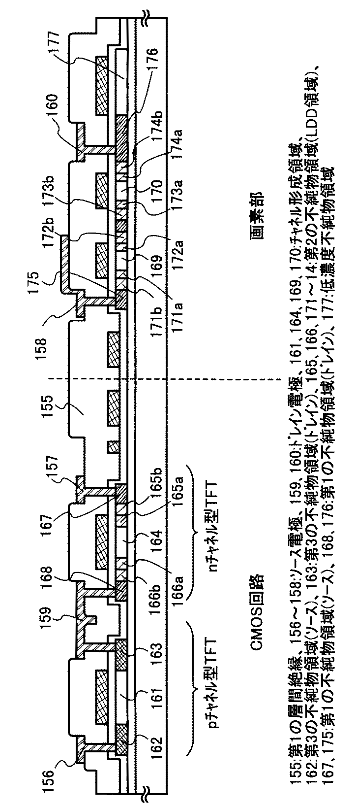
表1を参照すると前処理条件は水素を200SCCM導入し、圧力20Pa、高周波電力0.2W/cm2でプラズマを生成して2分間処理する。また、水素を100SCCMと酸素を100SCCM導入して同様にプラズマを生成して処理しても良い。また、表には記載しないがN2Oと水素を導入して圧力10〜70Pa、高周波電力密度0.1〜0.5 W/cm2で数分間処理しても良い。このような前処理のとき基板温度は300〜450℃、好ましくは400℃とすれば良い。前処理の効果は基板上の被堆積表面をクリーニングする作用や、被堆積表面に水素を吸着させ一時的に不活性化させることで、その後堆積される酸化窒化水素化シリコン膜の界面特性を安定化させる作用がある。また、酸素やN2Oを同時に導入することにより被堆積表面の最表面およびその近傍を酸化させ、界面準位密度を低減させるなどの好ましい作用がある。
【0024】
具体的には、酸化窒化水素化シリコン膜(B)の成膜条件は、#211の条件でSiH4を5SCCM、N2Oを120SCCM、水素を500SCCM、高周波電力密度0.4W/cm2とし、基板温度400℃で作製した。高周波電源周波数は10〜120MHz、好ましくは27〜60 MHzが適用され得るが、ここでは60 MHzとした。また、#212の条件では、#211の条件に対して水素の流量を125SCCMとして作製した。それぞれのガスの流量は、その絶対値を限定するものではなく流量比に意味を持っている。Xh=[H2]/([SiH4]+[N2O])とすると、Xhは0.1〜7の範囲とすれば良い。また、前述のように、Xg=[N2O]/([SiH4]+[N2O])とすると、Xgは0.90〜0.99の範囲とすれば良い。また、酸化窒化シリコン膜(A)の成膜条件は#210の条件である。
【0025】
このような条件で作製した酸化窒化シリコン膜の代表的な特性を表2に示す。表2には、ラザフォード・バックスキャッタリング・スペクトロメトリー(Rutherford Backscattering Spectrometry:以下、RBSと省略して記す。使用装置 システム;3S−R10、加速器;NEC3SDH pelletron エンドステーション;CE&A RBS−400)から求めた水素(H)、窒素(N)、酸素(O)、シリコン(Si)の組成と密度を示す。
【0026】
【表2】
表2の結果では、成膜時にH2を添加することで膜中に含まれる水素の濃度が増加している。これに伴い酸素や窒素の含有量も変化している。酸化窒化シリコン膜(A)ではSiに対するOの比が1.9(許容範囲として1.7〜2)であり、Siに対するNの比が0.04(許容範囲として0.02〜0.06)である。これに対し酸化窒化シリコン膜(B)の組成は、成膜時に添加するH2の流量で変化するものの、Siに対するOの比が1.6(許容範囲として1.4〜1.8)程度であり、Siに対するNの比が0.14〜0.18(許容範囲として0.05〜0.5)であり、Siに対してOの割合が低下し、窒素の割合が増加している。
【0028】
窒素含有量の増加は膜の密度の増加と対応しており、酸化窒化シリコン膜(A)の6.5atoms/cm3から、酸化窒化シリコン膜(B)では7.1atoms/cm3に増加し緻密化している。このような密度の変化はフッ化水素アンモニウム(NH4HF2)を7.13%とフッ化アンモニウム(NH4F)を15.4%含む混合溶液(ステラケミファ社製、商品名LAL500)の20℃におけるエッチング速度からも、酸化窒化シリコン膜(A)で120nm/minであるのに対し、酸化窒化シリコン膜(B)では63〜105nm/minであることから、窒素含有量の増加とともに膜が緻密化していくといえる。このことは、緻密で硬い膜は基板からの不純物のブロッキング性が高いことから酸化窒化シリコン膜(B)を基板側に設けることは有効であるということを示している。
【0029】
さらに、内部応力で比較すると、酸化窒化シリコン膜(A)は−4.26×10⁸Paの圧縮応力であるものが熱処理(500℃、1時間+550℃、4時間:結晶化の工程における処理条件と同等なもの)でが−7.29×10⁶Paに大きく変化する。一方、酸化窒化シリコン膜(B)は2.31×10⁸Paの引張り応力であり熱処理を施しても殆ど変化しない。熱処理により内部応力が変化する現象は膜の構造変化や組成変化と関連付けて考慮することができ、酸化窒化シリコン膜(B)の熱的安定性が良いといえる。
【0030】
以上のように、酸化窒化シリコン膜の特性について代表的な例を示した。勿論、本発明に適用し得る絶縁膜としての酸化窒化シリコン膜は表1、2で示したものに限定されるものではない。酸化窒化シリコン膜(A)の組成は、TFTに代表される半導体装置に適した下地膜として適した絶縁膜の組成は、窒素濃度1〜2atomic%、水素濃度0.5〜2atomic%、酸素濃度62〜65atomic%とする。酸化窒化シリコン膜(B)の組成は、窒素濃度7〜10atomic%、水素濃度2〜3atomic%、酸素濃度52〜55atomic%とする。さらに、酸化窒化シリコン膜(A)の密度は6×10²²以上7×10²²atoms/cm3未満とし、酸化窒化シリコン膜(B)の密度は7×1022以上8×1022atoms/cm3未満とする。上述のフッ化水素アンモニウム(NH4HF2)をとフッ化アンモニウム(NH4F)を含む混合溶液によるエッチング速度は、酸化窒化シリコン膜(A)で110〜130nm/minとし、酸化窒化シリコン膜(B)で60〜110nm/minとする。
【0031】
【発明の実施の形態】
本実施形態でTFTに代表される半導体装置に適した下地膜の作製方法について説明する。
【0032】
酸化窒化シリコン膜(A)と酸化窒化シリコン膜(B)をTFTの下地膜に適用する例を示す。図1(A)はトップゲート型のTFTの構成について示したものである。基板11上に下地膜(または、ブロッキング層ともいう)12が形成され、その上に島状半導体層13が形成されている。島状半導体層は非晶質半導体、結晶質半導体いずれの材料であっても良い。下地膜12は島状半導体層13の下面に接して形成されることになる。
【0033】
下地膜12は、膜厚方向に対して酸化窒化シリコン膜(A)から酸化窒化シリコン膜(B)に連続的または階段状に組成が変化する構成とする。図1(B)、(C)は酸化窒化シリコン膜の水素と窒素の組成を示すグラフである。上記構成の一例として、図1(B)に示すように酸化窒化シリコン膜(B)を島状半導体層に接して形成し、その上に酸化窒化シリコン膜(A)を形成する。または、図1(C)に示すように島状半導体層側から酸化窒化シリコン膜(B)から酸化窒化シリコン膜(A)に連続的に組成を変化させても良い。
【0034】
上記のように酸化窒化シリコン膜(A)と酸化窒化シリコン膜(B)を積層または連続的に組成を変化させることで、TFTの特性を安定化させることができる。具体的にはVthのシフトを防ぎ、熱的安定性による変動を防ぐことができる。
【0035】
図2は酸化窒化シリコン膜(A)と(B)を形成して、本発明の構成を得るのに適した装置の一例を示している。図2(A)に示すプラズマCVD装置は、ロード/アンロード室201、搬送室202、成膜室203を備えた装置である。各部屋は仕切弁204、205で分離されている。各部屋には真空ポンプなどを備えた減圧手段212a〜212cがそれぞれ接続している。ロード/アンロード室201には基板207と該基板を保持するカセット206があり、搬送室202に設けた搬送手段208により反応室203へ移送される。反応室203にはプラズマ発生手段209、基板加熱手段210、ガス供給手段211が備えられ、この部屋でグロー放電プラズマを利用した膜の形成が行われる。ガス供給手段211はSiH4、N2O、H2、O2などのガスが流量を制御して供給できるようになっている。
【0036】
反応室は1室のみの構成であるが、酸化窒化シリコン膜(A)と(B)はSiH4、N2O、H2の供給量や、高周波電力、反応圧力の制御ができるので同じ反応室で連続して形成することができる。むしろ、基板のサイズが大型化した場合には設置する床面積を小さくすることが可能となり省スペース化に寄与する。
【0037】
図2(B)に示す装置の構成は、ロード室220、アンロード室221、共通室222があり、共通室222の中に反応室223〜225が設けられた構成である。ロード室220、アンロード室221はそれぞれ基板236、238とそれを保持するカセット235、237が備えられ、仕切弁226、227で共通室と分離されている。ロード室220から搬送手段233により搬出された基板は反応室223〜225のいずれの部屋にもセットすることが可能である。
【0038】
反応室223〜225にはプラズマ発生手段240、基板加熱手段241、ガス供給手段239が備えられ、この部屋でグロー放電プラズマを利用した膜の形成が行われる。それぞれの反応室には仕切弁230a〜232a、230b〜232bが設けられ、真空ポンプなどを備えた減圧手段342により個別に圧力が制御できる。従って、成膜条件をそれぞれ個別に制御して膜の堆積をすることが可能である。または、それぞれの反応室で同時に、或いは並列して膜を形成することも可能であり生産性の向上を図ることもできる。
【0039】
酸化窒化シリコン膜(A)と(B)はSiH4、N2O、H2の供給量や、高周波電力、反応圧力の制御できるので同じ反応室で連続して形成することができ、上記膜の2層構造としても良いし、ガスの供給量を成膜時間と共に変化させて組成を連続的に変化させても良い。いずれにしても、図2(B)の装置の構成は生産性の向上に寄与する。
【0040】
【実施例】
[実施例1]
本発明を利用した酸化窒化シリコン膜と半導体膜(本実施例では結晶質シリコン膜)とを作製する工程について説明する。以下、図3を用いて本実施例を示す。
【0041】
本実施例では、図17に示す枚葉式のプラズマCVD装置(基板搬送室1711、ロードロック室1712、1713、第1の成膜チャンバー1714、第2の成膜チャンバー1715、ゲート弁1716〜1719等を備えた)を用いた。
【0042】
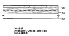
まず、ロードロック室1712のカセット1721に基板301をセットする。基板301にはコーニング社の7059ガラス基板や#1737ガラス基板に代表されるバリウムホウケイ酸ガラスやアルミノホウケイ酸ガラスなどを用いる。このようなガラス基板には微量ではあるが、ナトリウムなどのアルカリ金属元素などが含まれている。
【0043】
次いで、基板301を第1成膜チャンバー1714に搬入し、加熱して基板温度を約400℃にする。第1成膜チャンバー1714に搬入する前に、予熱室等を用いて基板を加熱してもよい。
【0044】
そして、図3に示すように基板301からのアルカリ金属元素やその他の不純物の汚染を防ぐためのブロッキング層として下地膜302を形成する。表1に記載された作製条件を基に、基板側との界面を酸化窒化シリコン膜(B)で形成し、その組成から酸化窒化シリコン膜(A)の組成へ連続的に組成が変化するようにSiH4、N2O、H2のガス流量をマスフローコントローラーで制御する。窒素含有量の多い酸化窒化シリコン膜(B)を基板側に設けることによって基板から活性層への不純物拡散を防止でき窒素含有量の少ない酸化窒化シリコン膜(A)を活性層側に設けることによって活性層と良好な界面状態を保つことができる。図3では組成が丁度中間の値を示すところを点線で示す。その部分は膜厚の中央部であっても良いし、半導体層寄り或いはゲート電極寄りであっても良い。具体的には、最初SiH4を5SCCM、N2Oを120SCCM、H2を125SCCM流し、Xh=1でXg=0.96とし、20Paに圧力を制御して27MHzで0.4mW/cm2の高周波電力を投入して成膜を開始し、その後成膜速度を考慮して随時N2O流量を成膜終了時に500SCCMとなるように増加させ、H2流量を0SCCMとして、Xh=0でXg=0.99となるように減少させる制御を行う。SiH4の流量は5SCCMから4SCCMへの制御なので、図3で示す点線のところで切り替えた。このようにして150nmの厚さで下地膜を形成した。勿論、下地膜の厚さはこれに限定されるものではなく、50〜300nm(好ましくは、80〜150nm)の厚さで形成し、前述のように酸化窒化シリコン膜(A)と(B)を積層する構造としても良い。尚、ここで示す成膜条件は一例であり、表2で示した組成が得られるならば成膜条件に何ら限定される事項はない。
【0045】
下地膜の成膜前に行うプラズマクリーニング処理は効果的である。また、プラズマクリーニング処理は、水素を200SCCM導入し、圧力20Pa、高周波電力0.2W/cm2でプラズマを生成して2分間処理する。或いは、H2を100SCCMと酸素を100SCCM導入して、圧力40Paで同様にプラズマ処理しても良い。また、N2Oと水素を導入して圧力10〜70Pa、高周波電力密度0.1〜0.5W/cm2で数分間処理してもよい。基板温度は300〜450℃、好ましくは400℃とする。この段階で、基板301の表面をプラズマクリーニング処理することで、吸着しているボロンやリン、その他の有機物などの汚染物質を取り除くことができる。
【0046】
こうして、膜中におけるN、O、Hの組成比が連続的に変化している酸化窒化シリコン膜12が得られる。この酸化窒化シリコン膜12は膜中において組成勾配を有しており、基板側の界面に向かって連続的に窒素及び水素が増加している。
【0047】
次いで、第1成膜チャンバー1714内のガスを真空引き、あるいはN2等の不活性ガスで置換した後、基板搬送室を経由して第2成膜チャンバー1715に基板を搬送する。
【0048】
次いで、酸化窒化シリコン膜302上に接して半導体膜303、ここでは非晶質シリコン膜を第2の成膜チャンバー1715で成膜した。
【0049】
ここでは、酸化窒化シリコン膜302と半導体膜とは、同じ成膜法で形成することが可能であるので両者を同一チャンバーで連続形成しても良い。連続成膜することによって、酸化窒化シリコン膜302の形成後、一旦搬送時の酸化窒化シリコン膜表面の汚染を防ぐことが可能となり、作製されるTFTの特性バラツキや閾値電圧の変動を低減させることができる。また、処理時間の短縮も図れ生産性が向上する。
【0050】
次いで、非晶質珪素膜が成膜された基板は、基板搬送室1711を経由してロードロック室1712に搬送され、カセット1722にセットされる。
【0051】
次いで、酸化窒化シリコン膜302と非晶質半導体膜とが積層形成された基板を公知の結晶化技術により結晶質半導体膜を形成した。
【0052】
以降の工程は、公知の技術を用いてTFTを形成すればよい。
【0053】
[実施例2]
以下、本発明の一実施例として同一基板上に画素マトリクス回路とドライバ回路を一体化したアクティブマトリクス型の液晶表示装置に適用した場合について、図4〜図10を用いて説明する。
【0054】
図4(A)は断面図であり、101は絶縁性基板であり、例えばコーニング社の1737ガラス基板である。このガラス基板上には、基板からの不純物拡散防止のための下地膜としてN、O、Hの組成比が連続的に変化している酸化窒化シリコン膜102と非晶質半導体膜103との積層膜を形成する。この積層膜の形成方法としてここでは、実施例1に示した方法を用い、膜厚150nmの下地膜と、膜厚50nmの非晶質シリコン膜とをそれぞれ形成した。
【0055】
次いで、非晶質シリコン膜は含有水素量にもよるが、好ましくは400〜550℃で数時間加熱して脱水素処理を行い、含有水素量を5atomic%以下として、結晶化の工程を行う。これにより、膜表面の荒れを防ぐことができる。プラズマCVD法にて非晶質シリコン膜を形成する場合、反応ガスにSiH4とArを用いて成膜時の基板温度を300〜400℃で形成すると、非晶質シリコン膜の含有水素濃度を5atomic%以下にすることもできる。このような場合には脱水素処理は不要となる。
【0056】
非晶質シリコン膜を結晶化する工程は、公知のレーザーアニール法または熱アニール法を用いれば良い。結晶化をレーザーアニール法で行う場合には、パルス発振型または連続発光型のエキシマレーザーやアルゴンレーザーをその光源とする。パルス発振型のエキシマレーザーを用いる場合にはレーザー光を線状に加工してレーザーアニールを行う。レーザーアニール条件は実施者が適宜選択するが、例えばレーザーパルス発振周波数30Hzとし、レーザーエネルギー密度を100〜500mJ/cm2(代表的には300〜400mJ/cm2)とする。そして、線状ビームを基板全面に渡って照射し、この時の線状ビームの重ね合わせ率(オーバーラップ率)を80〜90%として行う。このようにして、結晶質半導体層を形成することができる。また、別な方法としてパルス発振型のYAGレーザーを使用する方法がある。第2高調波(532nm)〜第3高調波を使用し、例えばレーザーパルス発振周波数1〜20000Hz(好ましくは10〜10000Hz)、レーザーエネルギー密度を200〜600mJ/cm2(代表的には300〜500mJ/cm2)とする。そして、線状ビームを基板全面に渡って照射し、この時の線状ビームの重ね合わせ率(オーバーラップ率)を80〜90%として行う。第2高調波を使うと、半導体層の内部にも均一に熱が伝わり、照射エネルギー範囲が多少ばらついても結晶化が可能となる。それにより、加工マージンがとれるため結晶化のばらつきが少なくなる。また、パルス周波数が高いのでスループットが向上する。熱アニール法による場合にはファーネスアニール炉を用い、窒素雰囲気で600〜660℃程度の温度でアニールを行う。いずれにしても非晶質半導体層を結晶化させると原子の再配列が起こり緻密化するので作製される結晶質半導体層の厚さは当初の非晶質半導体層の厚さよりも1〜15%程度減少する。本実施例では、パルス発振型のKrFエキシマレーザー光を線状に集光して非晶質シリコン膜に照射して結晶質シリコン膜を形成した。
【0057】
こうして形成された結晶質シリコン膜を第1のフォトマスクを使用して島状にパターニングし、ドライエッチングによりドライバ回路のpチャネルTFTの活性層103、nチャネルTFTの活性層104、画素TFTの活性層105を形成した。
【0058】
尚、本実施例では島状の半導体層を非晶質シリコン膜から結晶質シリコン膜を形成したが、微結晶シリコン膜を用いても構わないし、直接結晶質シリコン膜を成膜しても良い。
【0059】
次に、島状の半導体層103、104、105を覆って、酸化シリコンまたは窒化シリコンを主成分とするゲート絶縁膜106を形成した。ゲート絶縁膜106は、プラズマCVD法でN2OとSiH4を原料とした酸化窒化シリコン膜を10〜200nm、好ましくは50〜150 nmの厚さで形成すれば良い。ここでは100 nmの厚さに形成した。(図4(A))
【0060】
そして、第2のフォトマスクにより、半導体層103と、半導体層104、105のチャネル形成領域を覆うレジストマスク107、108、109、110、111を形成した。このとき、配線を形成する領域にもレジストマスク109を形成しておいても良い。
【0061】
そして、n型を付与する不純物元素を添加して第2の不純物領域を形成する工程を行った。ここでは、リンを用い、フォスフィン(PH3)を用いたイオンドープ法で行った。この工程では、ゲート絶縁膜106を通してその下の半導体層にリンを添加するために、加速電圧は80keVに設定した。半導体層に添加されるリンの濃度は、1×10¹⁶〜1×10¹⁹atoms/cm3の範囲にするのが好ましく、ここでは1×1018atoms/cm3とした。そして、半導体層にリンが添加された領域112、113、114、115、116が形成された。ここで、リンが添加された領域の一部は、LDD領域として機能する第2の不純物領域とされるものである。(図4(B))
【0062】
その後、レジストマスクを除去して、第1の導電層117を全面に形成した。第1の導電層117は、Ta、Ti、Mo、W、Cr、Alから選ばれた元素を主成分とする導電性材料やリンを含有するシリコンやシリサイドなどの単層膜あるいは積層膜から成る。例えば、WMo、TaN、MoTa、Wsix(2.4>x>2.7)などの化合物を用いることができる。そして、第1の導電層417の厚さは100〜1000nm、好ましくは150〜400nmで形成しておけば良い。ここではTaをスパッタ法で形成した。(図4(C))
【0063】
次に、第3のフォトマスクによりレジストマスク118、119、120、121、122、123を形成した。第3のフォトマスクは、pチャネル型TFTのゲート電極と、CMOS回路および画素部のゲート配線、ゲートバスラインを形成するためのものである。nチャネル型TFTのゲート電極は後の工程で形成するため、第1の導電層117が半導体層104、105上の全面で残るようにレジストマスク119、123を形成した。(図5(A))
【0064】
第1の導電層はドライエッチング法により不要な部分を除去した。TaのエッチングはCF4とO2の混合ガスにより行われた。そして、ゲート電極124と、ゲート配線126、128と、ゲートバスライン127が形成された。
【0065】
そして、レジストマスク118、119、120、121、122、123をそのまま残して、pチャネル型TFTが形成される半導体層103の一部に、p型を付与する第3の不純物元素を添加するの工程を行った。ここではボロンをその不純物元素として、ジボラン(B2H6)を用いてイオンドープ法で添加した。ここでも加速電圧を80keVとして、2×10²⁰atoms/cm3の濃度にボロンを添加した。そして、図5(A)に示すようにボロンが高濃度に添加された第3の不純物領域130、131が形成された。
【0066】
図5(A)で設けられたレジストマスクを除去した後、新たに第4のフォトマスクによりレジストマスク132、133、134、135、136、137、138を形成した。第4のフォトマスクはnチャネル型TFTのゲート電極を形成するためのものであり、ドライエッチング法によりゲート電極139、140、141及び容量電極142が形成された。このときゲート電極139、140、141は第2の不純物領域112、113、114、115、116の一部と重なるように形成された。(図5(B))
【0067】
そして、レジストマスクを除去した後、新たなレジストマスク143、144、145、146、147、148、149を形成した。レジストマスク144、147、148はnチャネル型TFTのゲート電極139、140、141と、第2の不純物領域の一部を覆う形で形成されるものであった。ここで、レジストマスク144、147、148は、LDD領域のオフセット量を決めるものであった。
【0068】
そして、n型を付与する不純物元素を添加して第1の不純物領域を形成する工程を行った。そして、ソース領域となる第1の不純物領域151、152とドレイン領域となる第1の不純物領域150、153、154が形成された。ここでは、フォスフィン(PH3)を用いたイオンドープ法で行った。この工程でも、ゲート絶縁膜106を通してその下の半導体層にリンを添加するために、加速電圧は80keVに設定した。この領域のリンの濃度はn型を付与する第1の不純物元素を添加する工程と比較して高濃度であり、1×10¹⁹〜1×10²¹atoms/cm3とするのが好ましく、ここでは1×1020atoms/cm3とした。(図5(C))
【0069】
図5(C)までの工程が終了したら、図6に示すように、ゲート電極およびゲート絶縁膜上に第1の層間絶縁膜155を形成する工程を行った。第1の層間絶縁膜は酸化シリコン膜、酸化窒化シリコン膜、窒化シリコン膜、またはこれらを組み合わせた積層膜で形成すれば良い。いずれにしても第1の層間絶縁膜155は無機絶縁物材料から形成する。第1の層間絶縁膜155の膜厚は100〜200nmとする。ここで、酸化シリコン膜を用いる場合には、プラズマCVD法でTEOSとO2とを混合し、反応圧力40Pa、基板温度300〜400℃とし、高周波(13.56MHz)電力密度0.5〜0.8W/cm2で放電させて形成することができる。また、酸化窒化シリコン膜を用いる場合には、プラズマCVD法でSiH4、N2O、NH3から作製される酸化窒化シリコン膜、またはSiH4、N2Oから作製される酸化窒化シリコン膜で形成すれば良い。この場合の作製条件は反応圧力20〜200Pa、基板温度300〜400℃とし、高周波(60MHz)電力密度0.1〜1.0W/cm2で形成することができる。また、SiH4、N2O、H2から作製される酸化窒化水素化シリコン膜を適用しても良い。窒化シリコン膜も同様にプラズマCVD法でSiH4、NH3から作製することが可能である。
【0070】
そして、熱処理の工程を行った。熱処理の工程は、それぞれの濃度で添加されたn型またはp型を付与する不純物元素を活性化するために行う必要があった。第1の層間絶縁膜が積層である場合、下層となる絶縁膜を成膜した後、熱処理工程を行うと良い。この工程は、電気加熱炉を用いた熱アニール法や、前述のエキシマレーザーを用いたレーザーアニール法や、ハロゲンランプを用いたラピットサーマルアニール法(RTA法)で行えば良い。ここでは熱アニール法で活性化の工程を行った。加熱処理は、酸素濃度が1ppm以下好ましくは0.1ppm以下の窒素雰囲気中において400〜700℃、好ましくは500〜600℃、ここでは500℃、4時間の処理を行った。
【0071】
熱活性化工程の後、さらに、3〜100%の水素を含む雰囲気中300~450℃で1~12時間の熱処理を行い、島状半導体層を水素化する工程を行った。この工程は熱的に励起された水素により半導体層のダングリングボンドを終端する工程である。水素化の他の手段としてプラズマ水素化(プラズマにより励起された水素を用いる)を行っても良い。いずれにしても、半導体層中の欠陥密度を1016/cm3以下とすることが望ましく、そのため、水素を0.01〜0.1atomic%程度付与すれば良い。
【0072】
第1の層間絶縁膜155はその後、パターニングでそれぞれのTFTのソース領域と、ドレイン領域に達するコンタクトホールが形成された。そして、ソース電極156、157、158とドレイン電極159、160を形成した。図示していないが、本実施例ではこの電極を、Ti膜を100nm、Tiを含むAl膜300nm、Ti膜150nmをスパッタ法で連続して成膜し、この3層膜をパターニングして電極として用いた。
【0073】
以上の工程で、CMOS回路のnチャネル型TFTにはチャネル形成領域164、第1の不純物領域167、168、第2の不純物領域165、166が形成された。ここで、第2の不純物領域は、ゲート電極と重なる領域(GOLD領域)165a、166a、ゲート電極と重ならない領域(LDD領域)165b、166bがそれぞれ形成された。そして、第1の不純物領域167はソース領域として、第1の不純物領域168はドレイン領域となった。
【0074】
pチャネル型TFTは、チャネル形成領域161、第3の不純物領域162、163が形成された。そして、第3の不純物領域162はソース領域として、第3の不純物領域163はドレイン領域となった。
【0075】
また、画素部のnチャネル型TFTはマルチゲート構造であり、チャネル形成領域169、170と第1の不純物領域175、176と第2の不純物領域171、172、173、174が形成された。ここで第2の不純物領域は、ゲート電極と重なる領域171a、172a、173a、174aと重ならない領域171b、172b、173b、174bとが形成された。
【0076】
こうして図6に示すように、基板101上にCMOS回路と、画素部が形成されたアクティブマトリクス基板が作製された。また、画素部のnチャネル型TFTのドレイン側には、第2の不純物領域と同じ濃度でn型を付与する不純物元素が添加された低濃度不純物領域177と、ゲート絶縁膜106と、容量電極142とにより保持容量が同時に形成された。
【0077】
次いで、アクティブマトリクス基板から、アクティブマトリクス型液晶表示装置を作製する工程を説明する。
【0078】
図6の状態のアクティブマトリクス基板に対して、パッシベーション膜178を形成した。パッシベーション膜178は、窒化シリコン膜で300nmの厚さで形成した。また、パッシベーション膜成膜後に水素化処理を行うとTFT特性向上に対して好ましい結果が得られている。例えば、3〜100%の水素を含む雰囲気中300〜450℃で1〜12時間の熱処理を行うと良く、あるいはプラズマ水素化法を用いても同様の効果が得られた。
【0079】
さらに、有機樹脂からなる第2の層間絶縁膜179を約1000nmの厚さに形成した。有機樹脂膜としては、ポリイミド、アクリル、ポリイミドアミド等を使用することができる。有機樹脂膜を用いることの利点は、成膜方法が簡単である点や、比誘電率が低いので、寄生容量を低減できる点、平坦性に優れる点などが上げられる。なお上述した以外の有機樹脂膜を用いることもできる。ここでは、基板に塗布後、熱重合するタイプのポリイミドを用い、300℃で焼成して形成した。(図7(A))
【0080】
さらに第3の層間絶縁膜180を形成した。第3の層間絶縁膜180は、ポリイミドなどの有機樹脂膜で形成した。そして、第3の層間絶縁膜180、第2の層間絶縁膜179、及びパッシベーション膜178を選択的に除去してドレイン電極160に達するコンタクトホールを形成し、画素電極181を形成した。画素電極181は、透過型液晶表示装置とする場合には透明導電膜を用い、反射型の液晶表示装置とする場合には金属膜を用いれば良い。ここでは透過型の液晶表示装置とするために、酸化インジウム・スズ(ITO)膜を100nmの厚さにスパッタ法で形成した後、パターニングして画素電極181を形成した。(図7(B))
【0081】
次に、図8に示すように、配向膜182を第3の層間絶縁膜180と画素電極181とに接して形成する。通常液晶表示素子の配向膜にはポリイミド樹脂が多く用いられている。対向側の基板183には、透明導電膜184と、配向膜185とを形成した。配向膜は形成された後、ラビング処理を施して液晶分子がある一定のプレチルト角を持って平行配向するようにした。
【0082】
上記の工程を経て、画素部と、CMOS回路が形成されたアクティブマトリクス基板と対向基板とを、公知のセル組み工程によってシール材やスペーサ(共に図示せず)などを介して貼りあわせる。その後、両基板の間に液晶材料186を注入し、封止剤(図示せず)によって完全に封止した。こうして図8に示すアクティブマトリクス型液晶表示装置が完成した。
【0083】
次に本実施例のアクティブマトリクス型液晶表示装置の構成を、図9と図10を用いて説明する。図9は本実施例のアクティブマトリクス基板の斜視図である。アクティブマトリクス基板は、ガラス基板101上に形成された、画素部901と、走査(ゲート)線駆動回路902と、信号(ソース)線駆動回路903と、ロジック回路904とで構成される。画素部の画素TFT900はnチャネル型TFTであり、周辺に設けられる駆動回路はCMOS回路を基本として構成されている。走査(ゲート)線駆動回路902と、信号(ソース)線駆動回路903はそれぞれゲート配線905とソース配線906で画素部901に接続されている。画素部901は画素TFT900と、画素電極907と、保持容量908とで形成される。
【0084】
本実施例では、画素TFT900をダブルゲートの構造としているが、シングルゲートの構造でも良いし、トリプルゲートとしたマルチゲート構造にしても構わない。本実施例のアクティブマトリクス基板の構造は、本実施例の構造に限定されるものではない。本願発明の構造は、下地膜の構成に特徴があるので、それ以外の構成については実施者が適宣決定すれば良い。
【0085】
図10は画素部901の上面図の一部であり、ほぼ1画素の上面図である。画素部にはnチャネル型TFTが設けられている。ゲート電極1002は、図示されていないゲート絶縁膜を介してその下の半導体層1001と交差している。図示はしていないが、半導体層には、ソース領域、ドレイン領域、第1の不純物領域が形成されている。また、画素TFTのドレイン側には、半導体層と、ゲート絶縁膜と、ゲート電極と同じ材料で形成された電極とから、保持容量1007が形成されている。また、図10で示すA―A'、およびB−B'に沿った断面構造は、図8に示す画素部の断面図に対応している。
【0086】
[実施例3]
本実施例では、実施例2において半導体層として用いる結晶質半導体膜を、触媒元素を用いた熱結晶化法により形成する例を示す。触媒元素を用いる場合、特開平7−130652号公報、特開平8−78329号公報で開示された技術を用いることが望ましい。
【0087】
ここで、特開平7−130652号公報に開示されている技術を本願発明に適用する場合の例を図11に示す。まず基板1101上下地膜としてN、O、Hの組成が連続的に変化している酸化窒化シリコン膜1102を設け、その上に非晶質シリコン膜1103を形成した。この積層膜の形成方法としてここでは、実施例1に示した方法を用い、膜厚200nmの下地膜と、膜厚50nmの非晶質シリコン膜とをそれぞれ形成した。
【0088】
次いで、図11(A)にあるように重量換算で10ppmの触媒元素であるニッケルを含む酢酸ニッケル塩溶液をスピンコーターで塗布した。これにより、結晶化を助長する元素であるニッケルが非晶質シリコン膜に添加され、ニッケル含有層1104が形成された。
【0089】
次に、500℃、1時間の脱水素工程により水素含有量を5atomic%以下にした後、500〜650℃で4〜12時間、例えば550℃、8時間の熱処理を行い、結晶質シリコン膜1105を形成した。こうして得られた結晶質シリコン膜1105は非常に優れた結晶性を示した。(図11(B))
【0090】
また、特開平8−78329号公報で開示された技術は、触媒元素を選択的に添加することによって、非晶質半導体膜の選択的な結晶化を可能としたものである。同技術を本願発明に適用した場合について、図12で説明する。
【0091】
まず、ガラス基板1201上にNまたはOの組成が連続的に変化している酸化窒化シリコン膜を含む下地膜1202を設け、その上に非晶質シリコン膜1203、酸化シリコン膜1204を連続的に形成した。この時、酸化シリコン膜1204の厚さは150nmとした。この下地膜1202の形成方法としてここでは、実施例1に示した方法を用いた下地膜を形成した。
【0092】
次に酸化シリコン膜1204をパターニングして、選択的に開孔部1205を形成し、その後、重量換算で10ppmのニッケルを含む酢酸ニッケル塩溶液を塗布した。これにより、ニッケル含有層1206が形成され、ニッケル含有層1206は開孔部1205の底部のみで非晶質シリコン膜1203と接触した。(図12(A))
【0093】
次に、500〜650℃で4〜24時間、例えば570℃、14時間の熱処理を行い、結晶質シリコン膜1207を形成した。この結晶化の過程では、ニッケルが接した非晶質シリコン膜の部分が最初に結晶化し、そこから横方向へと結晶化が進行する。こうして形成された結晶質シリコン膜1207は棒状または針状の結晶が集合して成り、その各々の結晶は巨視的に見ればある特定の方向性をもって成長しているため、結晶性が揃っているという利点がある。(図12(B))
【0094】
尚、上記2つの技術において使用可能な触媒元素は、ニッケル(Ni)の以外にも、ゲルマニウム(Ge)、鉄(Fe)、パラジウム(Pd)、スズ(Sn)、鉛(Pb)、コバルト(Co)、白金(Pt)、銅(Cu)、金(Au)、といった元素を用いても良い。
【0095】
以上のような技術を用いて結晶質半導体膜(結晶質シリコン膜や結晶質シリコンゲルマニウム膜などを含む)を形成し、パターニングを行えば、結晶質TFTの半導体層を形成することができる。本実施例の技術を用いて、結晶質半導体膜から作製されたTFTは、優れた特性が得られるが、そのため高い信頼性を要求されていた。しかしながら、本願発明のTFT構造を採用することで、本実施例の技術を最大限に生かしたTFTを作製することが可能となった。
【0096】
[実施例4]
本実施例は、実施例3で用いられる半導体層を形成する方法として、非晶質半導体膜を初期膜として前記触媒元素を用いて結晶質半導体膜を形成した後で、その触媒元素を結晶質半導体膜から除去する工程を行った例を示す。本実施例ではその方法として、特開平10−135468号公報または特開平10−135469号公報に記載された技術を用いた。
【0097】
同公報に記載された技術は、非晶質半導体膜の結晶化に用いた触媒元素を結晶化後にリンのゲッタリング作用を用いて除去する技術である。同技術を用いることで、結晶質半導体膜中の触媒元素の濃度を1×10¹⁷atms/cm3以下、好ましくは1×1016atms/cm3にまで低減することができる。
【0098】
本実施例の構成について図13を用いて説明する。ここではコーニング社の1737基板に代表される無アルカリガラス基板を用いた。図13(A)では、実施例3で示した結晶化の技術を用いて、基板1301上に下地膜1302、結晶質シリコン膜1303が形成された状態を示している。この下地膜1302の形成方法としてここでは、実施例1に示した方法を用いる。そして、結晶質シリコン膜1303の表面にマスク用の酸化シリコン膜1304が150nmの厚さに形成され、パターニングにより開孔部が設けられ、結晶質シリコン膜を露出させた領域を設けてある。そして、リンを添加する工程を実施して、結晶質シリコン膜にリンが添加された領域1305が設けられた。
【0099】
この状態で、窒素雰囲気中で550〜800℃、5〜24時間、例えば600℃、12時間の熱処理を行うと、結晶質シリコン膜にリンが添加された領域1305がゲッタリングサイトとして働き、結晶質シリコン膜1303に残存していた触媒元素はリンが添加された領域1305に偏析させることができた。
【0100】
そして、マスク用の酸化シリコン膜1304と、リンが添加された領域1305とをエッチングして除去することにより、結晶化の工程で使用した触媒元素の濃度を1×10¹⁷atms/cm3以下にまで低減された結晶質シリコン膜を得ることができた。この結晶質シリコン膜はそのまま実施例2で示した本願発明のTFTの半導体層として使用することができ、このようにして作製したTFTはオフ電流値が下がり結晶性が良いことから高い電界効果移動度が得られ、良好な特性が得られる。
【0101】
[実施例5]
本願発明を実施して形成されたTFTは様々な電気光学装置(代表的にはアクティブマトリクス型液晶ディスプレイ等)に用いることができる。即ち、それら電気光学装置や半導体回路を部品として組み込んだ電子機器全てに本願発明を実施できる。
【0102】
その様な電子機器としては、ビデオカメラ、デジタルカメラ、プロジェクター(リア型またはフロント型)、ヘッドマウントディスプレイ(ゴーグル型ディスプレイ)、カーナビゲーション、カーステレオ、パーソナルコンピュータ、携帯情報端末(モバイルコンピュータ、携帯電話または電子書籍等)などが挙げられる。それらの一例を図14、図15及び図16に示す。
【0103】
図14(A)はパーソナルコンピュータであり、本体1401、画像入力部1402、表示部1403、キーボード1404等を含む。本発明を画像入力部1402、表示部1403やその他の信号制御回路に適用することができる。
【0104】
図14(B)はビデオカメラであり、本体1405、表示部1406、音声入力部1407、操作スイッチ1408、バッテリー1409、受像部1410等を含む。本発明を表示部1406やその他の信号制御回路に適用することができる。
【0105】
図14(C)はモバイルコンピュータ(モービルコンピュータ)であり、本体1411、カメラ部1412、受像部1413、操作スイッチ1414、表示部1415等を含む。本発明は表示部1415やその他の信号制御回路に適用できる。
【0106】
図14(D)はゴーグル型ディスプレイであり、本体1416、表示部1417、アーム部1418等を含む。本発明は表示部1417やその他の信号制御回路に適用することができる。
【0107】
図14(E)はプログラムを記録した記録媒体(以下、記録媒体と呼ぶ)を用いるプレーヤーであり、本体1419、表示部1420、スピーカ部1421、記録媒体1422、操作スイッチ1423等を含む。なお、このプレーヤーは記録媒体としてDVD(Digital Versatile Disc)、CD等を用い、音楽鑑賞や映画鑑賞やゲームやインターネットを行うことができる。本発明は表示部1420やその他の信号制御回路に適用することができる。
【0108】
図14(F)はデジタルカメラであり、本体1424、表示部1425、接眼部1426、操作スイッチ1427、受像部(図示しない)等を含む。本願発明を表示部1425やその他の信号制御回路に適用することができる。
【0109】
図15(A)はフロント型プロジェクターであり、投射装置1501、スクリーン1502等を含む。本発明は投射装置1501の一部を構成する液晶表示装置1514やその他の信号制御回路に適用することができる。
【0110】
図15(B)はリア型プロジェクターであり、本体1503、投射装置1504、ミラー1505、スクリーン1506等を含む。本発明は投射装置1504の一部を構成する液晶表示装置1514やその他の信号制御回路に適用することができる。
【0111】
なお、図15(C)は、図15(A)及び図15(B)中における投射装置1501、1504の構造の一例を示した図である。投射装置1501、1504は、光源光学系1507、ミラー1508、1510〜1512、ダイクロイックミラー1509、プリズム1513、液晶表示装置1514、位相差板1515、投射光学系1516で構成される。投射光学系1516は、投射レンズを含む光学系で構成される。本実施例は三板式の例を示したが、特に限定されず、例えば単板式であってもよい。また、図15(C)中において矢印で示した光路に実施者が適宜、光学レンズや、偏光機能を有するフィルムや、位相差を調節するためのフィルム、IRフィルム等の光学系を設けてもよい。
【0112】
また、図15(D)は、図15(C)中における光源光学系1507の構造の一例を示した図である。本実施例では、光源光学系1507は、リフレクター1518、光源1519、レンズアレイ1520、1521、偏光変換素子1522、集光レンズ1523で構成される。なお、図15(D)に示した光源光学系は一例であって特に限定されない。例えば、光源光学系に実施者が適宜、光学レンズや、偏光機能を有するフィルムや、位相差を調節するフィルム、IRフィルム等の光学系を設けてもよい。
【0113】
ただし、図15に示したプロジェクターにおいては、透過型の電気光学装置を用いた場合を示しており、反射型の電気光学装置の適用例は図示していない。
【0114】
図16(A)は携帯電話であり、本体1601、音声出力部1602、音声入力部1603、表示部1604、操作スイッチ1605、アンテナ1606等を含む。本願発明を音声出力部1602、音声入力部1603、表示部1604やその他の信号制御回路に適用することができる。
【0115】
図16(B)は携帯書籍(電子書籍)であり、本体1607、表示部1608、記憶媒体1609、操作スイッチ1610、アンテナ1611等を含む。本発明は表示部1608、1609やその他の信号回路に適用することができる。
【0116】
図16(C)はディスプレイであり、本体1612、支持台1613、表示部1614等を含む。本発明は表示部1614に適用することができる。本発明のディスプレイは特に大画面化した場合において有利であり、対角10インチ以上(特に30インチ以上)のディスプレイには有利である。
【0117】
以上の様に、本願発明の適用範囲は極めて広く、あらゆる分野の電子機器に適用することが可能である。また、本実施例の電子機器は実施例1〜4のどのような組み合わせからなる構成を用いても実現することができる。
【0118】
【発明の効果】
こうして得られた本発明によるSiH4、N2O、H2を原料ガスとしてプラズマCVD法で作製される酸化窒化シリコン膜は、原料ガスの流量比を変化させるだけで作製することができ、それにより、膜中N、O、Hの組成の連続変化が制御された良質な下地膜として使用できる。本発明を下地膜として使用した場合、ブロッキング効果による基板からの不純物拡散の防止のみならず活性層と良好な界面を形成でき、TFT特性の劣化を防ぐことができる。また、同一チャンバーで成膜するため処理時間の短縮化が図れ、TFT特性の安定性向上並びに生産性向上にも寄与する。
【図面の簡単な説明】
【図1】 本発明の下地膜の構成を説明する図。
【図2】 本発明に適用するプラズマCVD装置の構成の一例を説明する図。
【図3】 本発明の作製工程を示す図。(実施例1)
【図4】 AM−LCDの作製工程を示す図。(実施例2)
【図5】 AM−LCDの作製工程を示す図。(実施例2)
【図6】 AM−LCDの作製工程を示す図。(実施例2)
【図7】 AM−LCDの作製工程を示す図。(実施例2)
【図8】 アクティブマトリクス型液晶表示装置の断面構造図。(実施例2)
【図9】 AM−LCDの外観を示す図。(実施例2)
【図10】 画素部上面図の一部を示す図。(実施例2)
【図11】 AM−LCDの作製工程を示す図。(実施例3)
【図12】 AM−LCDの作製工程を示す図。(実施例3)
【図13】 AM−LCDの作製工程を示す図。(実施例4)
【図14】 電子機器の一例を示す図。(実施例5)
【図15】 電子機器の一例を示す図。(実施例5)
【図16】 電子機器の一例を示す図。(実施例5)
【図17】 製造装置の一例を示す図。(実施例1)[0001]
BACKGROUND OF THE INVENTION
The present invention relates to a semiconductor device having a circuit formed of a thin film transistor (hereinafter referred to as TFT) and a manufacturing method thereof. For example, the present invention relates to an electro-optical device typified by an active matrix liquid crystal display device in which a pixel portion and a drive circuit are provided on the same substrate, and an electronic apparatus in which such an electro-optical device is mounted as a component.
[0002]
Note that in this specification, a semiconductor device refers to all devices that can function by utilizing semiconductor characteristics, an electro-optical device typified by an active matrix liquid crystal display device formed using thin film transistors, Electronic devices and semiconductor circuits each including such an electro-optical device as a component are all semiconductor devices.
[0003]
[Prior art]
Thin film transistors (TFTs) using semiconductor thin films formed on insulating substrates such as glass have been developed. As the semiconductor thin film material, an amorphous silicon film, a crystalline silicon film obtained by crystallizing an amorphous silicon film by a laser annealing method, a thermal annealing method, or the like is used. Above all, a TFT using a crystalline silicon film as an active layer has a high current drive capability due to its high electric field mobility, so that fine processing is possible and a high aperture ratio of the pixel portion can be achieved.
[0004]
Such TFTs are widely applied to electronic devices such as ICs and electro-optical devices, and are used, for example, in active matrix display devices applied to pixel switching elements and drive circuits. As the TFT substrate, a glass substrate such as barium borosilicate glass or alumino borosilicate is typically used. Although a glass substrate is inferior in heat resistance to a quartz substrate, it has an advantage that a large-area substrate can be easily manufactured at a low cost, so that a large-screen and inexpensive display device can be realized.
[0005]
In glass substrates, for example, barium borosilicate glass and aluminoborosilicate glass contain trace amounts of impurities such as alkali metal elements such as sodium (Na), and impurity ions enter the active layer from the glass substrate. TFT electrical characteristics fluctuate. In order to prevent this variation in electrical characteristics, a base layer (blocking layer) made of a silicon oxide film, a silicon nitride film, a silicon oxynitride film, or the like is formed on the surface of the glass substrate on which the TFT is formed.
[0006]
Further, it is known that the use of a laminated film in which a silicon nitride film is provided on the substrate side and a silicon oxide film is provided on the active layer side as the base film is effective in improving the stability of TFT characteristics.
[0007]
In the case of a top gate type TFT, since the channel formation region is in contact with the base film, the TFT characteristics are greatly influenced by the film quality of the base film.
[0008]
[Problems to be solved by the invention]
When a voltage is applied to the gate electrode of the TFT, an electric field is formed in the active layer, and impurity ions in the glass substrate are attracted to the active layer side. Therefore, depending on the film quality of the base film, impurity ions may enter the active layer and the gate insulating film through the base film, resulting in a change in the electrical characteristics of the TFT, leading to a decrease in reliability.
[0009]
The silicon nitride film as the underlying film has the advantage that the blocking effect of impurity ions is high, but has the disadvantage that there are many trap levels that affect the TFT characteristics, and furthermore, because the internal stress is large, forming an interface with the active layer Distortion causes TFT characteristics to deteriorate such as negative shift of Vth (threshold voltage) and increase of S value (subthreshold constant). In addition, a silicon oxide film as a base film has advantages such as a wider band gap, higher insulation, and lower trap level than a silicon nitride film, but it is easy to adsorb moisture and has a low impurity ion blocking effect. There are disadvantages. In the case of a silicon oxynitride film, its properties differ depending on the nitrogen concentration and oxygen concentration in the film, and it is necessary to increase the nitrogen concentration in the film and make the film dense in order to enhance the blocking effect of impurity ions. However, when the nitrogen concentration in the silicon oxynitride film is increased, the same defects as in the silicon nitride film occur.
[0010]
Furthermore, when a film containing a large amount of fixed charge is brought into contact with the active layer as the base film, trap levels are formed at the interface between the base film and the active layer, leading to a decrease in TFT characteristics. In general, the fixed charge increases as the nitrogen concentration in the film increases.
[0011]
In addition, when the silicon nitride film and the silicon oxide film are stacked, the respective constituent elements are different, so that a dedicated film forming chamber is required. In this case, since the temperature of the film formation chamber is lowered when the substrate is cooled during the conveyance of the substrate, preheating is required to prevent the substrate temperature from being lowered. This preheating time led to an increase in processing time.
[0012]
The present invention is a technique for solving the above-described problems, and an object of the present invention is to provide a base film excellent in stability and reliability of TFT characteristics and productivity, and a manufacturing method thereof.
[0013]
[Means for Solving the Problems]
In order to solve the above problems, the present invention is based on the plasma CVD method. Four , N 2 O, H 2 Then, a silicon oxynitride film is formed using this, and this film is applied to the base of the TFT. The characteristics of the fabricated silicon oxynitride film are mainly N 2 O and H 2 Control by changing the flow rate. H 2 By increasing the flow rate, the hydrogen concentration and nitrogen concentration in the film can be increased within the above ranges. N 2 By increasing the flow rate of O, the hydrogen concentration and nitrogen concentration in the film can be reduced and the oxygen concentration can be increased. Meanwhile, H 2 And N 2 Even if only the gas flow ratio of O is changed, the concentration of silicon hardly changes. As a result, a silicon oxynitride film having a composition exhibiting the merit of the silicon nitride film is continuously formed on the substrate side, and a silicon oxynitride film having a composition exhibiting the merit of the silicon oxide film is continuously formed on the active layer side. Therefore, it is possible to manufacture a good quality base film that takes advantage of both the silicon nitride film and the silicon oxide film. Further, since the silicon oxynitride film showing the film quality is the same in the film forming method only by changing the gas flow rate ratio, the film can be formed in the same film forming chamber, thereby improving the productivity.
[0014]
Specifically, SiH Four , N 2 O, H 2 The flow ratio of Xh = 0.5-5 (Xh = H 2 / SiH Four + N 2 O) Xg = 0.94-0.97 (Xg = N 2 O / SiH Four + N 2 O) and a silicon oxynitride film formed in the range of Xh = 0 (Xh = H 2 / SiH Four + N 2 O), Xg = 0.97-0.99 (Xg = N 2 O / SiH Four + N 2 A silicon oxynitride film formed in the range of O) is formed, and these silicon oxynitride films are selectively used.
[0015]
When producing silicon oxynitride films by plasma CVD, SiH Four And N 2 H to mixed gas of O 2 By adding SiH Four It is possible to prevent radicals generated from decomposition from being polymerized in the gas phase (in the reaction space) and to eliminate generation of particles. In addition, it is possible to prevent excessive hydrogen from being taken into the film due to the extraction reaction of surface adsorbed hydrogen by hydrogen radicals on the film growth surface. Such an action has a close correlation with the substrate temperature during film deposition, and the action can be obtained by setting the substrate temperature to 300 to 400 ° C., preferably 400 ° C. As a result, it is possible to form a dense film with a low defect density, and a trace amount of hydrogen contained in the film works effectively as an action of relaxing lattice strain. In order to decompose hydrogen and increase the generation density of hydrogen radicals, the high frequency power source frequency for generating glow discharge is 13.56 to 120 MHz, preferably 27 to 60 MHz, and the discharge power density is 0.1 to 1 W / cm. 2 And
[0016]
By adopting the above manufacturing conditions, the composition of the silicon oxynitride film applied to the present invention is such that the nitrogen concentration is 0.5 atomic% or more and less than 10 atomic%, the hydrogen concentration is 0.5 atomic% or more and less than 5 atomic%, and the oxygen concentration is 50 atomic%. % And less than 70 atomic%.
[0017]
The feature of the present invention is that, when forming a TFT base film with a silicon oxynitride film, at least the composition of the base film is different between the substrate side and the active layer side. The concentration and hydrogen concentration are high and the oxygen concentration is low.
[0018]
For example, the first layer in contact with the base film substrate is formed of a silicon oxynitride film having a nitrogen concentration of 7 to 10 atomic%, a hydrogen concentration of 2 to 3 atomic%, and an oxygen concentration of 52 to 55 atomic%, and the second layer in contact with the active layer The eyes are formed of a silicon oxynitride film having a nitrogen concentration of 1 to 2 atomic%, a hydrogen concentration of 0.5 to 2 atomic%, and an oxygen concentration of 62 to 65 atomic%, and a stepwise concentration gradient is provided. Alternatively, the composition may be continuously changed without clear distinction between the first layer and the second layer as described above.
[0019]
For the production of the silicon oxynitride film, the structure of the plasma apparatus is a capacitively coupled parallel plate type. In addition, a plasma CVD apparatus using magnetic field energy such as inductive coupling type or electron cyclotron resonance may be used. Silicon oxynitride film is SiH Four , N 2 O gas is used and H 2 Can be added to change the composition. Pressure during plasma formation is 10 to 133 Pa (preferably 20 to 40 Pa), high frequency power density 0.2 to 1 W / cm 2 (Preferably 0.3 to 0.5 W / cm 2 ), The substrate temperature is 200 to 450 ° C. (preferably 300 to 400 ° C.), and the oscillation frequency of the high frequency power source is 10 to 120 MHz (preferably 27 to 60 MHz).
[0020]
Table 1 lists three types of manufacturing conditions.
[0021]
Table 1 also describes pretreatment conditions to be performed before the formation of the silicon oxynitride film. Although this pretreatment is not essential, it is useful for improving the reproducibility of the silicon oxynitride film characteristics and the reproducibility of the characteristics when applied to a TFT.
[0022]
[Table 1]
Referring to Table 1, the pretreatment conditions are 200 SCCM of hydrogen, pressure 20 Pa, high frequency power 0.2 W / cm 2 Generate plasma and process for 2 minutes. Alternatively, 100 SCCM of hydrogen and 100 SCCM of oxygen may be introduced and plasma may be generated and processed in the same manner. N not shown in the table 2 O and hydrogen introduced, pressure 10 ~ 70Pa, high frequency power density 0.1 ~ 0.5 W / cm 2 May be processed for several minutes. In such pretreatment, the substrate temperature may be 300 to 450 ° C., preferably 400 ° C. The effect of pretreatment is to stabilize the interface characteristics of the silicon oxynitride film deposited afterwards by cleaning the deposition surface on the substrate and by temporarily inactivating hydrogen by adsorbing it to the deposition surface. There is an action to make it. Also oxygen and N 2 By introducing O at the same time, the outermost surface of the surface to be deposited and its vicinity are oxidized, and there is a preferable action such as reducing the interface state density.
[0024]
Specifically, the silicon oxynitride silicon film (B) is formed under the conditions of # 211 with SiH Four 5SCCM,
[0025]
Table 2 shows typical characteristics of a silicon oxynitride film manufactured under such conditions. In Table 2, it was obtained from Rutherford Backscattering Spectrometry (hereinafter abbreviated as RBS. Equipment used; system 3S-R10, accelerator; NEC3SDH pelletron end station; CE & A RBS-400). The composition and density of hydrogen (H), nitrogen (N), oxygen (O), and silicon (Si) are shown.
[0026]
[Table 2]
The results in Table 2 show that H 2 Adding hydrogen increases the concentration of hydrogen contained in the film. Along with this, the contents of oxygen and nitrogen are also changing. In the silicon oxynitride film (A), the ratio of O to Si is 1.9 (allowable range is 1.7 to 2), and the ratio of N to Si is 0.04 (allowable range is 0.02 to 0.06). In contrast, the composition of the silicon oxynitride film (B) is H 2 The ratio of O to Si is about 1.6 (acceptable range is 1.4 to 1.8), and the ratio of N to Si is 0.14 to 0.18 (allowable range is 0.05 to 0.5). The proportion of O decreases and the proportion of nitrogen increases.
[0028]
The increase in nitrogen content corresponds to the increase in film density, and 6.5 atoms / cm of silicon oxynitride film (A) Three To 7.1 atoms / cm for silicon oxynitride film (B) Three It is increasing and becoming denser. This change in density is caused by ammonium hydrogen fluoride (NH Four HF 2 ) 7.13% and ammonium fluoride (NH Four The etching rate at 20 ° C of the mixed solution containing 15.4% of F) (product name: LAL500, manufactured by Stella Chemifa) is 120 nm / min for the silicon oxynitride film (A), whereas the silicon oxynitride film (B ) 63-105 nm / min, it can be said that the film becomes denser as the nitrogen content increases. This indicates that it is effective to provide the silicon oxynitride film (B) on the substrate side because the dense and hard film has a high blocking property of impurities from the substrate.
[0029]
Furthermore, when compared with internal stress, the silicon oxynitride film (A) is -4.26 × 10 8 The Pa compressive stress is heat treatment (500 ° C, 1 hour + 550 ° C, 4 hours: equivalent to the treatment conditions in the crystallization process) -7.29 × 10 6 It changes greatly to Pa. On the other hand, the silicon oxynitride film (B) is 2.31 × 10 8 It is a tensile stress of Pa and hardly changes even after heat treatment. The phenomenon that the internal stress changes due to the heat treatment can be considered in relation to the structural change and composition change of the film, and it can be said that the thermal stability of the silicon oxynitride film (B) is good.
[0030]
As described above, typical examples of the characteristics of the silicon oxynitride film are shown. Of course, the silicon oxynitride film as an insulating film applicable to the present invention is not limited to those shown in Tables 1 and 2. The composition of the silicon oxynitride film (A) is as follows. The composition of the insulating film suitable as a base film suitable for a semiconductor device represented by TFT is as follows: nitrogen concentration 1 to 2 atomic%, hydrogen concentration 0.5 to 2 atomic%, oxygen concentration 62 to 65 atomic%. The composition of the silicon oxynitride film (B) is a nitrogen concentration of 7 to 10 atomic%, a hydrogen concentration of 2 to 3 atomic%, and an oxygen concentration of 52 to 55 atomic%. Furthermore, the density of the silicon oxynitride film (A) is 6 × 10 twenty two 7 × 10 or more twenty two atoms / cm Three And the density of the silicon oxynitride film (B) is 7 × 10 twenty two 8 × 10 or more twenty two atoms / cm Three Less than. Ammonium hydrogen fluoride (NH Four HF 2 ) And ammonium fluoride (NH Four The etching rate with the mixed solution containing F) is 110 to 130 nm / min for the silicon oxynitride film (A) and 60 to 110 nm / min for the silicon oxynitride film (B).
[0031]
DETAILED DESCRIPTION OF THE INVENTION
In this embodiment, a method for manufacturing a base film suitable for a semiconductor device typified by a TFT will be described.
[0032]
An example in which the silicon oxynitride film (A) and the silicon oxynitride film (B) are applied to a TFT base film is shown. Fig. 1 (A) shows the structure of a top-gate TFT. A base film (or a blocking layer) 12 is formed on the
[0033]
The
[0034]
As described above, the characteristics of the TFT can be stabilized by laminating or continuously changing the composition of the silicon oxynitride film (A) and the silicon oxynitride film (B). Specifically, the shift of Vth can be prevented and fluctuation due to thermal stability can be prevented.
[0035]
FIG. 2 shows an example of an apparatus suitable for forming the silicon oxynitride films (A) and (B) to obtain the structure of the present invention. The plasma CVD apparatus illustrated in FIG. 2A is an apparatus including a load / unload
[0036]
Although there is only one reaction chamber, the silicon oxynitride films (A) and (B) are made of SiH. Four , N 2 O, H 2 Since the supply amount, high-frequency power, and reaction pressure can be controlled, they can be formed continuously in the same reaction chamber. Rather, when the size of the substrate is increased, the floor area to be installed can be reduced, contributing to space saving.
[0037]
The structure of the apparatus illustrated in FIG. 2B includes a
[0038]
The
[0039]
Silicon oxynitride films (A) and (B) are SiH Four , N 2 O, H 2 Can be formed continuously in the same reaction chamber, and it can be a two-layer structure of the above-mentioned film, or the gas supply amount can be changed with the film formation time. The composition may be changed continuously. In any case, the configuration of the apparatus in FIG. 2B contributes to the improvement of productivity.
[0040]
【Example】
[Example 1]
A process for manufacturing a silicon oxynitride film and a semiconductor film (crystalline silicon film in this embodiment) using the present invention will be described. Hereinafter, this embodiment will be described with reference to FIG.
[0041]
In this embodiment, the single-wafer type plasma CVD apparatus (
[0042]
First, the
[0043]
Next, the
[0044]
Then, as shown in FIG. 3, a
[0045]
A plasma cleaning process performed before forming the base film is effective. The plasma cleaning process introduces 200SCCM of hydrogen, pressure 20Pa, high frequency power 0.2W / cm 2 Generate plasma and process for 2 minutes. Or H 2 100 SCCM and 100 SCCM of oxygen may be introduced, and plasma treatment may be similarly performed at a pressure of 40 Pa. N 2 O and hydrogen introduced, pressure 10 ~ 70Pa, high frequency power density 0.1 ~ 0.5W / cm 2 May be processed for several minutes. The substrate temperature is 300 to 450 ° C., preferably 400 ° C. At this stage, the surface of the
[0046]
Thus, the
[0047]
Next, the gas in the first film formation chamber 1714 is evacuated or N 2 Then, the substrate is transferred to the second film formation chamber 1715 via the substrate transfer chamber.
[0048]
Next, a
[0049]
Here, since the
[0050]
Next, the substrate on which the amorphous silicon film is formed is transferred to the
[0051]
Next, a crystalline semiconductor film was formed by a known crystallization technique on the substrate on which the
[0052]
In the subsequent steps, a TFT may be formed using a known technique.
[0053]
[Example 2]
Hereinafter, a case where the present invention is applied to an active matrix type liquid crystal display device in which a pixel matrix circuit and a driver circuit are integrated on the same substrate will be described with reference to FIGS.
[0054]
4A is a cross-sectional view, 101 is an insulating substrate, for example, a 1737 glass substrate manufactured by Corning. On this glass substrate, a laminated layer of a
[0055]
Next, although depending on the hydrogen content, the amorphous silicon film is preferably heated at 400 to 550 ° C. for several hours for dehydrogenation treatment, and the crystallization process is performed with the hydrogen content being 5 atomic% or less. Thereby, roughening of the film surface can be prevented. When forming an amorphous silicon film by plasma CVD, SiH is used as the reaction gas. Four When using Ar and Ar to form a substrate at 300 to 400 ° C., the hydrogen concentration in the amorphous silicon film can be reduced to 5 atomic% or less. In such a case, the dehydrogenation process is unnecessary.
[0056]
A known laser annealing method or thermal annealing method may be used for the step of crystallizing the amorphous silicon film. When crystallization is performed by laser annealing, a pulse oscillation type or continuous light emission type excimer laser or argon laser is used as the light source. When a pulse oscillation type excimer laser is used, laser annealing is performed by processing the laser beam into a linear shape. The laser annealing conditions are appropriately selected by the practitioner. For example, the laser pulse oscillation frequency is 30 Hz, and the laser energy density is 100 to 500 mJ / cm. 2 (Typically 300-400mJ / cm 2 ). Then, the linear beam is irradiated over the entire surface of the substrate, and the linear beam superposition ratio (overlap ratio) at this time is set to 80 to 90%. In this way, a crystalline semiconductor layer can be formed. Another method is to use a pulse oscillation type YAG laser. 2nd harmonic (532nm) to 3rd harmonic are used, for example, laser pulse oscillation frequency 1 to 20000Hz (preferably 10 to 10,000Hz), laser energy density 200 to 600mJ / cm 2 (Typically 300-500mJ / cm 2 ). Then, the linear beam is irradiated over the entire surface of the substrate, and the linear beam superposition ratio (overlap ratio) at this time is set to 80 to 90%. When the second harmonic is used, heat is evenly transmitted to the inside of the semiconductor layer, and crystallization is possible even if the irradiation energy range varies somewhat. As a result, a processing margin can be obtained, and variations in crystallization are reduced. Further, since the pulse frequency is high, the throughput is improved. In the case of thermal annealing, a furnace annealing furnace is used and annealing is performed at a temperature of about 600 to 660 ° C. in a nitrogen atmosphere. In any case, when the amorphous semiconductor layer is crystallized, the rearrangement of atoms occurs and it becomes dense, so the thickness of the crystalline semiconductor layer produced is 1-15% than the thickness of the original amorphous semiconductor layer Decrease degree. In this embodiment, a pulsed oscillation type KrF excimer laser beam is condensed into a linear shape and irradiated to an amorphous silicon film to form a crystalline silicon film.
[0057]
The crystalline silicon film thus formed is patterned into an island shape using a first photomask, and the
[0058]
In this embodiment, a crystalline silicon film is formed from an amorphous silicon film as an island-shaped semiconductor layer. However, a microcrystalline silicon film may be used, or a crystalline silicon film may be directly formed. .
[0059]
Next, a
[0060]
Then, resist
[0061]
Then, an impurity element imparting n-type was added to form a second impurity region. Here, phosphorus is used and phosphine (PH Three ) Using an ion doping method. In this step, the acceleration voltage was set to 80 keV in order to add phosphorus to the underlying semiconductor layer through the
[0062]
Thereafter, the resist mask was removed, and a first
[0063]
Next, resist
[0064]
An unnecessary portion of the first conductive layer was removed by a dry etching method. Ta etching is CF Four And O 2 The mixed gas was used. Then, the
[0065]
Then, a third impurity element imparting p-type conductivity is added to part of the
[0066]
After the resist mask provided in FIG. 5A was removed, resist
[0067]
Then, after removing the resist mask, new resist
[0068]
Then, a step of forming the first impurity region by adding an impurity element imparting n-type was performed. Then,
[0069]
When the steps up to FIG. 5C were completed, a step of forming a first
[0070]
And the process of heat processing was performed. The heat treatment step must be performed to activate the impurity element imparting n-type or p-type added at each concentration. In the case where the first interlayer insulating film is a stacked layer, a heat treatment step may be performed after forming an insulating film as a lower layer. This step may be performed by a thermal annealing method using an electric heating furnace, a laser annealing method using the above-described excimer laser, or a rapid thermal annealing method (RTA method) using a halogen lamp. Here, the activation process was performed by thermal annealing. The heat treatment was performed in a nitrogen atmosphere having an oxygen concentration of 1 ppm or less, preferably 0.1 ppm or less, at 400 to 700 ° C., preferably 500 to 600 ° C., here 500 ° C. for 4 hours.
[0071]
After the thermal activation step, a heat treatment was performed at 300 to 450 ° C. for 1 to 12 hours in an atmosphere containing 3 to 100% hydrogen to hydrogenate the island-shaped semiconductor layer. This step is a step of terminating dangling bonds in the semiconductor layer with thermally excited hydrogen. Plasma hydrogenation (using hydrogen excited by plasma) may be performed as another means of hydrogenation. In any case, it is desirable that the defect density in the semiconductor layer be 10 16 / cm 3 or less, and therefore, hydrogen may be added at about 0.01 to 0.1 atomic%.
[0072]
The first
[0073]
Through the above steps, the
[0074]
In the p-channel TFT, a
[0075]
Further, the n-channel TFT in the pixel portion has a multi-gate structure, and
[0076]
Thus, as shown in FIG. 6, an active matrix substrate having a CMOS circuit and a pixel portion formed on a
[0077]
Next, a process for manufacturing an active matrix liquid crystal display device from an active matrix substrate will be described.
[0078]
A passivation film 178 was formed on the active matrix substrate in the state shown in FIG. The passivation film 178 was formed of a silicon nitride film with a thickness of 300 nm. In addition, when the hydrogenation treatment is performed after the passivation film is formed, a favorable result is obtained for improving the TFT characteristics. For example, heat treatment may be performed at 300 to 450 ° C. for 1 to 12 hours in an atmosphere containing 3 to 100% hydrogen, or the same effect can be obtained by using a plasma hydrogenation method.
[0079]
Further, a second interlayer insulating film 179 made of an organic resin was formed to a thickness of about 1000 nm. As the organic resin film, polyimide, acrylic, polyimide amide, or the like can be used. Advantages of using the organic resin film are that the film forming method is simple, the relative dielectric constant is low, the parasitic capacitance can be reduced, and the flatness is excellent. Organic resin films other than those described above can also be used. Here, it was formed by baking at 300 ° C. using a type of polyimide that is thermally polymerized after being applied to the substrate. (Fig. 7 (A))
[0080]
Further, a third interlayer insulating film 180 was formed. The third interlayer insulating film 180 was formed of an organic resin film such as polyimide. Then, the third interlayer insulating film 180, the second interlayer insulating film 179, and the passivation film 178 were selectively removed to form a contact hole reaching the
[0081]
Next, as shown in FIG. 8, an alignment film 182 is formed in contact with the third interlayer insulating film 180 and the pixel electrode 181. Usually, a polyimide resin is often used for the alignment film of the liquid crystal display element. A transparent conductive film 184 and an alignment film 185 were formed on the opposite substrate 183. After the alignment film was formed, it was rubbed so that the liquid crystal molecules were aligned in parallel with a certain pretilt angle.
[0082]
Through the above steps, the pixel portion, the active matrix substrate on which the CMOS circuit is formed, and the counter substrate are bonded to each other through a sealing material, a spacer (both not shown), and the like by a known cell assembling process. Thereafter, a liquid crystal material 186 was injected between both substrates and completely sealed with a sealant (not shown). Thus, the active matrix liquid crystal display device shown in FIG. 8 was completed.
[0083]
Next, the configuration of the active matrix liquid crystal display device of this embodiment will be described with reference to FIGS. FIG. 9 is a perspective view of the active matrix substrate of this example. The active matrix substrate includes a
[0084]
In this embodiment, the
[0085]
FIG. 10 is a part of a top view of the
[0086]
[Example 3]
In this example, an example in which a crystalline semiconductor film used as a semiconductor layer in Example 2 is formed by a thermal crystallization method using a catalytic element is shown. In the case of using a catalyst element, it is desirable to use the techniques disclosed in Japanese Patent Application Laid-Open Nos. 7-130652 and 8-78329.
[0087]
Here, FIG. 11 shows an example in which the technique disclosed in Japanese Patent Laid-Open No. 7-130652 is applied to the present invention. First, a silicon oxynitride film 1102 in which the composition of N, O, and H was continuously changed was provided as a base film over a substrate 1101, and an amorphous silicon film 1103 was formed thereon. As a method for forming this laminated film, here, the method shown in Example 1 was used, and a base film having a thickness of 200 nm and an amorphous silicon film having a thickness of 50 nm were formed.
[0088]
Next, as shown in FIG. 11 (A), a nickel acetate salt solution containing nickel as a catalytic element at 10 ppm in terms of weight was applied by a spin coater. As a result, nickel, which is an element that promotes crystallization, was added to the amorphous silicon film, and a nickel-containing layer 1104 was formed.
[0089]
Next, after the hydrogen content is reduced to 5 atomic% or less by a dehydrogenation process at 500 ° C. for 1 hour, a heat treatment is performed at 500 to 650 ° C. for 4 to 12 hours, for example, 550 ° C. for 8 hours, and the crystalline silicon film 1105 Formed. The crystalline silicon film 1105 obtained in this way showed very good crystallinity. (Fig. 11 (B))
[0090]
Further, the technique disclosed in Japanese Patent Laid-Open No. 8-78329 enables selective crystallization of an amorphous semiconductor film by selectively adding a catalytic element. The case where this technology is applied to the present invention will be described with reference to FIG.
[0091]
First, a base film 1202 including a silicon oxynitride film in which the composition of N or O is continuously changed is provided over a glass substrate 1201, and an amorphous silicon film 1203 and a silicon oxide film 1204 are continuously formed thereon. Formed. At this time, the thickness of the silicon oxide film 1204 was set to 150 nm. Here, as a method for forming the base film 1202, a base film using the method shown in Example 1 was formed.
[0092]
Next, the silicon oxide film 1204 was patterned to selectively form the
[0093]
Next, heat treatment was performed at 500 to 650 ° C. for 4 to 24 hours, for example, 570 ° C. for 14 hours, thereby forming a crystalline silicon film 1207. In this crystallization process, the portion of the amorphous silicon film in contact with nickel is crystallized first, and then proceeds laterally from there. The crystalline silicon film 1207 thus formed is a collection of rod-like or needle-like crystals, and each crystal grows with a specific direction as viewed macroscopically, so that the crystallinity is uniform. There is an advantage. (Fig. 12 (B))
[0094]
In addition to nickel (Ni), the catalyst elements that can be used in the above two technologies are germanium (Ge), iron (Fe), palladium (Pd), tin (Sn), lead (Pb), cobalt ( Elements such as Co), platinum (Pt), copper (Cu), and gold (Au) may be used.
[0095]
A crystalline TFT semiconductor layer can be formed by forming a crystalline semiconductor film (including a crystalline silicon film or a crystalline silicon germanium film) using the above-described technique and performing patterning. A TFT manufactured from a crystalline semiconductor film using the technique of this embodiment can provide excellent characteristics, but high reliability has been required. However, by adopting the TFT structure of the present invention, it has become possible to produce a TFT that makes the most of the technique of this embodiment.
[0096]
[Example 4]
In this example, as a method of forming a semiconductor layer used in Example 3, an amorphous semiconductor film is used as an initial film and a crystalline semiconductor film is formed using the catalytic element. The example which performed the process removed from a semiconductor film is shown. In the present embodiment, the technique described in Japanese Patent Application Laid-Open No. 10-135468 or Japanese Patent Application Laid-Open No. 10-135469 is used as the method.
[0097]
The technique described in the publication is a technique for removing a catalytic element used for crystallization of an amorphous semiconductor film by using a gettering action of phosphorus after crystallization. By using this technology, the concentration of the catalytic element in the crystalline semiconductor film is reduced to 1 × 10 17 atms / cm Three Below, preferably 1 × 10 16 atms / cm Three It can be reduced to.
[0098]
The configuration of this example will be described with reference to FIG. Here, an alkali-free glass substrate typified by Corning's 1737 substrate was used. FIG. 13A shows a state in which a base film 1302 and a crystalline silicon film 1303 are formed over a substrate 1301 by using the crystallization technique shown in Embodiment 3. Here, the method shown in Embodiment 1 is used as a method for forming the base film 1302. A silicon oxide film 1304 for a mask is formed to a thickness of 150 nm on the surface of the crystalline silicon film 1303, an opening is provided by patterning, and a region where the crystalline silicon film is exposed is provided. Then, a step of adding phosphorus was performed to provide a
[0099]
In this state, when heat treatment is performed in a nitrogen atmosphere at 550 to 800 ° C. for 5 to 24 hours, for example, 600 ° C. for 12 hours, a
[0100]
Then, the silicon oxide film 1304 for mask and the
[0101]
[Example 5]
A TFT formed by implementing the present invention can be used in various electro-optical devices (typically, active matrix liquid crystal displays). That is, the present invention can be implemented in all electronic devices in which these electro-optical devices and semiconductor circuits are incorporated as parts.
[0102]
Such electronic devices include video cameras, digital cameras, projectors (rear or front type), head mounted displays (goggles type displays), car navigation systems, car stereos, personal computers, personal digital assistants (mobile computers, mobile phones) Or an electronic book). Examples of these are shown in FIGS.
[0103]
FIG. 14A shows a personal computer, which includes a main body 1401, an image input portion 1402, a display portion 1403, a
[0104]
FIG. 14B illustrates a video camera, which includes a main body 1405, a display portion 1406, an audio input portion 1407, operation switches 1408, a battery 1409, an image receiving portion 1410, and the like. The present invention can be applied to the display portion 1406 and other signal control circuits.
[0105]
FIG. 14C illustrates a mobile computer, which includes a main body 1411, a
[0106]
FIG. 14D shows a goggle type display, which includes a main body 1416, a
[0107]
FIG. 14E shows a player using a recording medium (hereinafter referred to as a recording medium) on which a program is recorded, and includes a main body 1419, a
[0108]
FIG. 14F illustrates a digital camera, which includes a main body 1424, a
[0109]
FIG. 15A illustrates a front type projector, which includes a
[0110]
FIG. 15B illustrates a rear projector, which includes a main body 1503, a
[0111]
FIG. 15C is a diagram showing an example of the structure of the
[0112]
FIG. 15D is a diagram illustrating an example of the structure of the light source
[0113]
However, the projector shown in FIG. 15 shows a case where a transmissive electro-optical device is used, and an application example of the reflective electro-optical device is not shown.
[0114]
FIG. 16A illustrates a mobile phone, which includes a main body 1601, an
[0115]
FIG. 16B illustrates a portable book (electronic book), which includes a
[0116]
FIG. 16C illustrates a display which includes a main body 1612, a
[0117]
As described above, the application range of the present invention is extremely wide and can be applied to electronic devices in various fields. Further, the electronic apparatus of the present embodiment can be realized by using a configuration including any combination of the first to fourth embodiments.
[0118]
【The invention's effect】
The SiH according to the invention thus obtained Four , N 2 O, H 2 A silicon oxynitride film fabricated by plasma CVD using as a source gas can be fabricated simply by changing the flow rate ratio of the source gas, thereby controlling the continuous change in the composition of N, O, and H in the film. It can be used as a high quality undercoat film. When the present invention is used as a base film, not only the diffusion of impurities from the substrate due to the blocking effect but also a good interface with the active layer can be formed, and the deterioration of TFT characteristics can be prevented. In addition, since the film is formed in the same chamber, the processing time can be shortened, which contributes to improved stability of TFT characteristics and improved productivity.
[Brief description of the drawings]
FIG. 1 is a diagram illustrating a configuration of a base film of the present invention.
FIG. 2 illustrates an example of a structure of a plasma CVD apparatus applied to the present invention.
FIGS. 3A and 3B illustrate a manufacturing process of the present invention. FIGS. Example 1
4A and 4B are diagrams illustrating a manufacturing process of an AM-LCD. (Example 2)
FIGS. 5A and 5B are diagrams illustrating a manufacturing process of an AM-LCD. FIGS. (Example 2)
6A and 6B are diagrams illustrating a manufacturing process of an AM-LCD. (Example 2)
7A and 7B are diagrams illustrating a manufacturing process of an AM-LCD. (Example 2)
FIG. 8 is a cross-sectional structure diagram of an active matrix liquid crystal display device. (Example 2)
FIG. 9 is a diagram illustrating an appearance of an AM-LCD. (Example 2)
FIG. 10 is a diagram showing a part of a top view of a pixel portion. (Example 2)
FIG. 11 is a diagram showing a manufacturing process of an AM-LCD. (Example 3)
12A and 12B are diagrams illustrating a manufacturing process of an AM-LCD. (Example 3)
13A and 13B are diagrams illustrating a manufacturing process of an AM-LCD. (Example 4)
FIG 14 illustrates an example of an electronic device. (Example 5)
FIG 15 illustrates an example of an electronic device. (Example 5)
FIG 16 illustrates an example of an electronic device. (Example 5)
FIG. 17 shows an example of a manufacturing apparatus. Example 1
Claims (16)
基板に接して絶縁膜と、
前記絶縁膜上に接して半導体膜とを有し、
前記絶縁膜は、少なくとも前記基板と接する第1の層と前記半導体膜と接する第2の層とを有し、
前記第1の層は、水素濃度が2〜3atomic%で、窒素濃度が7〜10atomic%で、酸素濃度が52〜55atomic%の酸化窒化シリコン膜であり、
前記第2の層は、水素濃度が0.5〜2atomic%で、窒素濃度が1〜2atomic%で、酸素濃度が62〜65atomic%の酸化窒化シリコン膜であることを特徴とする半導体装置。A semiconductor device having a thin film transistor,
An insulating film in contact with the substrate,
A semiconductor film in contact with the insulating film;
The insulating film has at least a first layer in contact with the substrate and a second layer in contact with the semiconductor film ;
The first layer is the hydrogen concentration is 2 ~ 3 atomic%, a nitrogen concentration of 7 ~ 10 atomic%, the oxygen concentration is silicon oxynitride film of 52 ~ 55 atomic%,
2. The semiconductor device according to claim 1, wherein the second layer is a silicon oxynitride film having a hydrogen concentration of 0.5 to 2 atomic%, a nitrogen concentration of 1 to 2 atomic%, and an oxygen concentration of 62 to 65 atomic%.
基板に接して絶縁膜と、
前記絶縁膜上に接して半導体膜とを有し、
前記絶縁膜は、前記基板と接する領域から前記半導体膜と接する領域にかけて連続的に組成が変化し、
前記基板と接する領域は、水素濃度が2〜3atomic%で、窒素濃度が7〜10atomic%で、酸素濃度が52〜55atomic%の酸化窒化シリコン膜であり、
前記半導体膜と接する領域は、水素濃度が0.5〜2atomic%で、窒素濃度が1〜2atomic%で、酸素濃度が62〜65atomic%の酸化窒化シリコン膜であることを特徴とする半導体装置。A semiconductor device having a thin film transistor,
An insulating film in contact with the substrate,
A semiconductor film in contact with the insulating film;
The insulating film continuously changes in composition from a region in contact with the substrate to a region in contact with the semiconductor film ,
The region in contact with the substrate is a silicon oxynitride film having a hydrogen concentration of 2 to 3 atomic%, a nitrogen concentration of 7 to 10 atomic%, and an oxygen concentration of 52 to 55 atomic%.
A region in contact with the semiconductor film is a silicon oxynitride film having a hydrogen concentration of 0.5 to 2 atomic%, a nitrogen concentration of 1 to 2 atomic%, and an oxygen concentration of 62 to 65 atomic%.
基板に接して絶縁膜と、
前記絶縁膜上に接して半導体膜とを有し、
前記絶縁膜は、少なくとも前記基板と接する第1の層と前記半導体膜と接する第2の層とを有し、
前記第1の層は、シリコンに対する酸素の組成比が1.4〜1.8で、シリコンに対する窒素の組成比が0.05〜0.5の酸化窒化シリコン膜であり、
前記第2の層は、シリコンに対する酸素の組成比が1.7〜2で、シリコンに対する窒素の組成比が0.02〜0.06の酸化窒化シリコン膜であることを特徴とする半導体装置。A semiconductor device having a thin film transistor,
An insulating film in contact with the substrate,
A semiconductor film in contact with the insulating film;
The insulating film has at least a first layer in contact with the substrate and a second layer in contact with the semiconductor film ;
The first layer is a silicon oxynitride film having a composition ratio of oxygen to silicon of 1.4 to 1.8 and a composition ratio of nitrogen to silicon of 0.05 to 0.5.
The semiconductor device, wherein the second layer is a silicon oxynitride film having a composition ratio of oxygen to silicon of 1.7 to 2 and a composition ratio of nitrogen to silicon of 0.02 to 0.06.
基板に接して絶縁膜と、
前記絶縁膜上に接して半導体膜とを有し、
前記絶縁膜は、前記基板と接する領域から前記半導体膜と接する領域にかけて連続的に組成が変化し、
前記基板と接する領域は、シリコンに対する酸素の組成比が1.4〜1.8で、シリコンに対する窒素の組成比が0.05〜0.5の酸化窒化シリコン膜であり、
前記半導体膜と接する領域は、シリコンに対する酸素の組成比が1.7〜2で、シリコンに対する窒素の組成比が0.02〜0.06の酸化窒化シリコン膜であることを特徴とする半導体装置。A semiconductor device having a thin film transistor,
An insulating film in contact with the substrate,
A semiconductor film in contact with the insulating film;
The insulating film continuously changes in composition from a region in contact with the substrate to a region in contact with the semiconductor film ,
The region in contact with the substrate is a silicon oxynitride film having a composition ratio of oxygen to silicon of 1.4 to 1.8 and a composition ratio of nitrogen to silicon of 0.05 to 0.5.
The region in contact with the semiconductor film is a silicon oxynitride film having a composition ratio of oxygen to silicon of 1.7 to 2 and a composition ratio of nitrogen to silicon of 0.02 to 0.06. .
前記絶縁膜を形成する工程は、少なくとも前記基板と界面を形成する第1の層を形成する工程と、前記半導体膜と界面を形成する第2の層を形成する工程とを有し、
前記第1の層を形成する工程は、SiH4、N2O、H2のガス流量比がXh=0.5〜5(Xh=H2/SiH4+N2O)、Xg=0.94〜0.97(Xg=N2O/SiH4+N2O)の範囲で酸化窒化シリコン膜を形成し、
前記第2の層を形成する工程は、SiH4、N2O、H2のガス流量比がXh=0(Xh=H2/SiH4+N2O)、Xg=0.97〜0.99(Xg=N2O/SiH4+N2O)範囲で酸化窒化シリコン膜を形成することを特徴とする半導体装置の作製方法。Forming a semiconductor film, and forming an insulating film between the semiconductor film and the substrate,
Wherein the step of forming the insulating film, and a step of forming a step of forming a first layer that forms at least the substrate and the interface, the second layer for forming the semiconductor layer and the interface,
In the step of forming the first layer, the gas flow ratio of SiH 4 , N 2 O, and H 2 is Xh = 0.5 to 5 (Xh = H 2 / SiH 4 + N 2 O), Xg = 0.94 A silicon oxynitride film is formed in a range of ˜0.97 (Xg = N 2 O / SiH 4 + N 2 O),
In the step of forming the second layer, the gas flow ratio of SiH 4 , N 2 O, and H 2 is Xh = 0 (Xh = H 2 / SiH 4 + N 2 O), Xg = 0.97 to 0.99. A method for manufacturing a semiconductor device, wherein a silicon oxynitride film is formed in a range of (Xg = N 2 O / SiH 4 + N 2 O).
前記絶縁膜を形成する工程は、前記基板と接する領域から前記半導体膜と接する領域にかけて、SiH4、N2O、H2のガス流量比がXh=0.5〜5(Xh=H2/SiH4+N2O)、Xg=0.94〜0.97(Xg=N2O/SiH4+N2O)の範囲から、Xh=0(Xh=H2/SiH4+N2O)、Xg=0.97〜0.99(Xg=N2O/SiH4+N2O)の範囲に変化させて酸化窒化シリコン膜を形成することを特徴とする半導体装置の作製方法。Forming a semiconductor film, and forming an insulating film between the semiconductor film and the substrate,
In the step of forming the insulating film, the gas flow rate ratio of SiH 4 , N 2 O, and H 2 from the region in contact with the substrate to the region in contact with the semiconductor film is Xh = 0.5 to 5 (Xh = H 2 / SiH 4 + N 2 O), Xg = 0.94-0.97 (Xg = N 2 O / SiH 4 + N 2 O), Xh = 0 (Xh = H 2 / SiH 4 + N 2 O), Xg = 0.97~0.99 (Xg = N 2 O / SiH 4 + N 2 O) the method for manufacturing a semiconductor device according range is changed and forming a silicon oxynitride film of.
水素濃度が2〜3atomic%で、窒素濃度が7〜10atomic%で、酸素濃度が52〜55atomic%の基板と接する第1の酸化窒化シリコン膜と、
水素濃度が0.5〜2atomic%で、窒素濃度が1〜2atomic%で、酸素濃度が62〜65atomic%の半導体膜と接する第2の酸化窒化シリコン膜と、
前記半導体膜とを連続的に成膜することを特徴とする半導体装置の作製方法。In the same deposition chamber
A first silicon oxynitride film in contact with a substrate having a hydrogen concentration of 2 to 3 atomic%, a nitrogen concentration of 7 to 10 atomic%, and an oxygen concentration of 52 to 55 atomic%;
A second silicon oxynitride film in contact with a semiconductor film having a hydrogen concentration of 0.5 to 2 atomic%, a nitrogen concentration of 1 to 2 atomic%, and an oxygen concentration of 62 to 65 atomic%;
A method for manufacturing a semiconductor device, wherein the semiconductor film is continuously formed.
基板と接する領域は、水素濃度が2〜3atomic%で、窒素濃度が7〜10atomic%で、酸素濃度が52〜55atomic%、
半導体膜と接する領域は、水素濃度が0.5〜2atomic%で、窒素濃度が1〜2atomic%で、酸素濃度が62〜65atomic%と連続的に組成が変化する酸化窒化シリコン膜と、
前記半導体膜とを連続的に成膜することを特徴とする半導体装置の作製方法。In the same deposition chamber
Region in contact with the substrate, hydrogen concentration 2 ~ 3 atomic%, a nitrogen concentration of 7 ~ 10 atomic%, an oxygen concentration of 52 ~ 55 atomic%,
A region in contact with the semiconductor film is a silicon oxynitride film having a hydrogen concentration of 0.5 to 2 atomic%, a nitrogen concentration of 1 to 2 atomic%, and an oxygen concentration of 62 to 65 atomic%, the composition of which continuously changes.
A method for manufacturing a semiconductor device, wherein the semiconductor film is continuously formed.
シリコンに対する酸素の組成比が1.4〜1.8で、シリコンに対する窒素の組成比が0.05〜0.5の基板と接する第1の酸化窒化シリコン膜と、
シリコンに対する酸素の組成比が1.7〜2で、シリコンに対する窒素の組成比が0.02〜0.06の半導体膜と接する第2の酸化窒化シリコン膜と、
前記半導体膜とを連続的に成膜することを特徴とする半導体装置の作製方法。In the same deposition chamber
A first silicon oxynitride film in contact with a substrate having a composition ratio of oxygen to silicon of 1.4 to 1.8 and a composition ratio of nitrogen to silicon of 0.05 to 0.5;
A second silicon oxynitride film in contact with the semiconductor film having a composition ratio of oxygen to silicon of 1.7 to 2 and a composition ratio of nitrogen to silicon of 0.02 to 0.06;
A method for manufacturing a semiconductor device, wherein the semiconductor film is continuously formed.
基板と接する領域は、シリコンに対する酸素の組成比が1.4〜1.8で、シリコンに対する窒素の組成比が0.05〜0.5、
半導体膜と接する領域は、シリコンに対する酸素の組成比が1.7〜2で、シリコンに対する窒素の組成比が0.02〜0.06と連続的に組成が変化する酸化窒化シリコン膜と、
前記半導体膜とを連続的に成膜することを特徴とする半導体装置の作製方法。In the same deposition chamber
The region in contact with the substrate has a composition ratio of oxygen to silicon of 1.4 to 1.8, and a composition ratio of nitrogen to silicon of 0.05 to 0.5,
The region in contact with the semiconductor film has a silicon oxynitride film in which the composition ratio of oxygen to silicon is 1.7 to 2 and the composition ratio of nitrogen to silicon is 0.02 to 0.06 and the composition changes continuously;
A method for manufacturing a semiconductor device, wherein the semiconductor film is continuously formed.
Priority Applications (3)
| Application Number | Priority Date | Filing Date | Title |
|---|---|---|---|
| JP2000022022A JP4493779B2 (en) | 2000-01-31 | 2000-01-31 | Semiconductor device and manufacturing method thereof |
| TW090101346A TW479370B (en) | 2000-01-31 | 2001-01-19 | Semiconductor device and method of producing the same |
| US09/771,625 US6673659B2 (en) | 2000-01-31 | 2001-01-30 | Semiconductor device and method of producing the same |
Applications Claiming Priority (1)
| Application Number | Priority Date | Filing Date | Title |
|---|---|---|---|
| JP2000022022A JP4493779B2 (en) | 2000-01-31 | 2000-01-31 | Semiconductor device and manufacturing method thereof |
Publications (3)
| Publication Number | Publication Date |
|---|---|
| JP2001217422A JP2001217422A (en) | 2001-08-10 |
| JP2001217422A5 JP2001217422A5 (en) | 2006-11-16 |
| JP4493779B2 true JP4493779B2 (en) | 2010-06-30 |
Family
ID=18548367
Family Applications (1)
| Application Number | Title | Priority Date | Filing Date |
|---|---|---|---|
| JP2000022022A Expired - Fee Related JP4493779B2 (en) | 2000-01-31 | 2000-01-31 | Semiconductor device and manufacturing method thereof |
Country Status (3)
| Country | Link |
|---|---|
| US (1) | US6673659B2 (en) |
| JP (1) | JP4493779B2 (en) |
| TW (1) | TW479370B (en) |
Families Citing this family (26)
| Publication number | Priority date | Publication date | Assignee | Title |
|---|---|---|---|---|
| US6573195B1 (en) * | 1999-01-26 | 2003-06-03 | Semiconductor Energy Laboratory Co., Ltd. | Method for manufacturing a semiconductor device by performing a heat-treatment in a hydrogen atmosphere |
| US6461899B1 (en) | 1999-04-30 | 2002-10-08 | Semiconductor Energy Laboratory, Co., Ltd. | Oxynitride laminate “blocking layer” for thin film semiconductor devices |
| CN100485943C (en) * | 1999-06-02 | 2009-05-06 | 株式会社半导体能源研究所 | Semiconductor device |
| JP4562835B2 (en) * | 1999-11-05 | 2010-10-13 | 株式会社半導体エネルギー研究所 | Method for manufacturing semiconductor device |
| JP2001177101A (en) | 1999-12-20 | 2001-06-29 | Semiconductor Energy Lab Co Ltd | Semiconductor device and method of manufacturing the same |
| JP2004247077A (en) * | 2003-02-12 | 2004-09-02 | Semiconductor Energy Lab Co Ltd | Light-emitting device and its manufacturing method |
| DE10335099B4 (en) * | 2003-07-31 | 2006-06-08 | Advanced Micro Devices, Inc., Sunnyvale | Method for improving the thickness uniformity of silicon nitride layers for a plurality of semiconductor wafers |
| JP4232675B2 (en) * | 2004-04-01 | 2009-03-04 | セイコーエプソン株式会社 | Manufacturing method of semiconductor device |
| JP4649896B2 (en) | 2004-07-09 | 2011-03-16 | 日本電気株式会社 | Semiconductor device, manufacturing method thereof, and display device including the semiconductor device |
| US20060181266A1 (en) * | 2005-02-14 | 2006-08-17 | Panelvision Technology, A California Corporation | Flat panel display inspection system |
| KR101133767B1 (en) * | 2005-03-09 | 2012-04-09 | 삼성전자주식회사 | Organic thin film transistor array panel and method for manufacturing the same |
| JP2006269808A (en) * | 2005-03-24 | 2006-10-05 | Mitsubishi Electric Corp | Semiconductor device and image display device |
| KR100703971B1 (en) * | 2005-06-08 | 2007-04-06 | 삼성전자주식회사 | Semiconductor integrated circuit device and method for fabricating the same |
| EP1998375A3 (en) * | 2005-09-29 | 2012-01-18 | Semiconductor Energy Laboratory Co, Ltd. | Semiconductor device having oxide semiconductor layer and manufacturing method |
| US7498270B2 (en) * | 2005-09-30 | 2009-03-03 | Tokyo Electron Limited | Method of forming a silicon oxynitride film with tensile stress |
| US7588883B2 (en) | 2006-05-09 | 2009-09-15 | United Microelectronics Corp. | Method for forming a gate and etching a conductive layer |
| JP2008258345A (en) * | 2007-04-04 | 2008-10-23 | Sony Corp | Thin film transistor, its manufacturing method, and display unit |
| US7807586B2 (en) * | 2008-03-28 | 2010-10-05 | Tokyo Electron Limited | Method of forming a stressed passivation film using a non-ionizing electromagnetic radiation-assisted oxidation process |
| US8119540B2 (en) * | 2008-03-28 | 2012-02-21 | Tokyo Electron Limited | Method of forming a stressed passivation film using a microwave-assisted oxidation process |
| JP5458102B2 (en) * | 2009-09-04 | 2014-04-02 | 株式会社東芝 | Thin film transistor manufacturing method |
| DE102010013038B4 (en) * | 2010-03-26 | 2012-01-19 | Schüco Tf Gmbh & Co. Kg | Method for producing a photovoltaic cell |
| JP5827578B2 (en) | 2011-02-14 | 2015-12-02 | 株式会社半導体エネルギー研究所 | Method for producing optical element |
| CN103828061B (en) * | 2011-10-07 | 2018-02-13 | 应用材料公司 | Carry out the method for deposit silicon-containing materials using argon-dilution |
| JP6026395B2 (en) * | 2013-12-05 | 2016-11-16 | 富士フイルム株式会社 | Substrate with organic functional layer and method for producing the same |
| KR102223678B1 (en) | 2014-07-25 | 2021-03-08 | 삼성디스플레이 주식회사 | Backplane for display apparatus and manufacturing method thereof |
| CN108493238B (en) * | 2018-03-28 | 2022-11-25 | 京东方科技集团股份有限公司 | Thin film transistor, manufacturing method, array substrate and display device |
Citations (3)
| Publication number | Priority date | Publication date | Assignee | Title |
|---|---|---|---|---|
| JP2000269510A (en) * | 1998-12-29 | 2000-09-29 | Semiconductor Energy Lab Co Ltd | Semiconductor device and its manufacture |
| JP2001015764A (en) * | 1999-04-30 | 2001-01-19 | Semiconductor Energy Lab Co Ltd | Semiconductor device and manufacture thereof |
| JP2001177101A (en) * | 1999-12-20 | 2001-06-29 | Semiconductor Energy Lab Co Ltd | Semiconductor device and method of manufacturing the same |
Family Cites Families (10)
| Publication number | Priority date | Publication date | Assignee | Title |
|---|---|---|---|---|
| US5470768A (en) | 1992-08-07 | 1995-11-28 | Fujitsu Limited | Method for fabricating a thin-film transistor |
| US5923962A (en) | 1993-10-29 | 1999-07-13 | Semiconductor Energy Laboratory Co., Ltd. | Method for manufacturing a semiconductor device |
| TW264575B (en) | 1993-10-29 | 1995-12-01 | Handotai Energy Kenkyusho Kk | |
| JP3431033B2 (en) | 1993-10-29 | 2003-07-28 | 株式会社半導体エネルギー研究所 | Semiconductor fabrication method |
| JP3464287B2 (en) | 1994-09-05 | 2003-11-05 | 株式会社半導体エネルギー研究所 | Method for manufacturing semiconductor device |
| JP3597331B2 (en) | 1996-10-24 | 2004-12-08 | 株式会社半導体エネルギー研究所 | Method for manufacturing semiconductor device |
| JP3645377B2 (en) | 1996-10-24 | 2005-05-11 | 株式会社半導体エネルギー研究所 | Integrated circuit fabrication method |
| JP2000012864A (en) | 1998-06-22 | 2000-01-14 | Semiconductor Energy Lab Co Ltd | Manufacture of semiconductor device |
| US6461899B1 (en) | 1999-04-30 | 2002-10-08 | Semiconductor Energy Laboratory, Co., Ltd. | Oxynitride laminate “blocking layer” for thin film semiconductor devices |
| TW521226B (en) | 2000-03-27 | 2003-02-21 | Semiconductor Energy Lab | Electro-optical device |
-
2000
- 2000-01-31 JP JP2000022022A patent/JP4493779B2/en not_active Expired - Fee Related
-
2001
- 2001-01-19 TW TW090101346A patent/TW479370B/en not_active IP Right Cessation
- 2001-01-30 US US09/771,625 patent/US6673659B2/en not_active Expired - Lifetime
Patent Citations (3)
| Publication number | Priority date | Publication date | Assignee | Title |
|---|---|---|---|---|
| JP2000269510A (en) * | 1998-12-29 | 2000-09-29 | Semiconductor Energy Lab Co Ltd | Semiconductor device and its manufacture |
| JP2001015764A (en) * | 1999-04-30 | 2001-01-19 | Semiconductor Energy Lab Co Ltd | Semiconductor device and manufacture thereof |
| JP2001177101A (en) * | 1999-12-20 | 2001-06-29 | Semiconductor Energy Lab Co Ltd | Semiconductor device and method of manufacturing the same |
Also Published As
| Publication number | Publication date |
|---|---|
| US6673659B2 (en) | 2004-01-06 |
| TW479370B (en) | 2002-03-11 |
| JP2001217422A (en) | 2001-08-10 |
| US20010011725A1 (en) | 2001-08-09 |
Similar Documents
| Publication | Publication Date | Title |
|---|---|---|
| JP4493779B2 (en) | Semiconductor device and manufacturing method thereof | |
| US9786787B2 (en) | Semiconductor device and fabrication method thereof | |
| KR100736400B1 (en) | Semiconductor Device and Method for Its Fabrication | |
| JP3538084B2 (en) | Method for manufacturing semiconductor device | |
| JP4798907B2 (en) | Semiconductor device | |
| US6777713B2 (en) | Irregular semiconductor film, having ridges of convex portion | |
| JP2001177101A (en) | Semiconductor device and method of manufacturing the same | |
| JP4667523B2 (en) | Semiconductor device and manufacturing method thereof | |
| JP2001135824A (en) | Semiconductor device and manufacturing method thereof | |
| US6727124B2 (en) | Method of manufacturing a TFT using a catalytic element to promote crystallization of a semiconductor film and gettering the catalytic element | |
| JP4094179B2 (en) | Method for manufacturing semiconductor device | |
| JP4683696B2 (en) | Method for manufacturing semiconductor device | |
| JP4494451B2 (en) | Method for manufacturing semiconductor device | |
| JP4080168B2 (en) | Method for manufacturing semiconductor device | |
| JP4641586B2 (en) | Method for manufacturing semiconductor device | |
| JP4766724B2 (en) | Method for manufacturing semiconductor device | |
| JP4256087B2 (en) | Method for manufacturing semiconductor device | |
| JP4472061B2 (en) | Method for manufacturing semiconductor device | |
| JP5057605B2 (en) | Method for manufacturing semiconductor device | |
| JP4573953B2 (en) | Method for manufacturing semiconductor device | |
| JP4700159B2 (en) | Method for manufacturing semiconductor device | |
| JP4712155B2 (en) | Method for manufacturing semiconductor device | |
| JP5072147B2 (en) | Method for manufacturing semiconductor device | |
| JP4993802B2 (en) | Semiconductor device | |
| JP5256336B2 (en) | Liquid crystal display |
Legal Events
| Date | Code | Title | Description |
|---|---|---|---|
| A521 | Request for written amendment filed |
Free format text: JAPANESE INTERMEDIATE CODE: A523 Effective date: 20060927 |
|
| A621 | Written request for application examination |
Free format text: JAPANESE INTERMEDIATE CODE: A621 Effective date: 20060927 |
|
| A977 | Report on retrieval |
Free format text: JAPANESE INTERMEDIATE CODE: A971007 Effective date: 20100129 |
|
| A131 | Notification of reasons for refusal |
Free format text: JAPANESE INTERMEDIATE CODE: A131 Effective date: 20100209 |
|
| A521 | Request for written amendment filed |
Free format text: JAPANESE INTERMEDIATE CODE: A523 Effective date: 20100316 |
|
| TRDD | Decision of grant or rejection written | ||
| A01 | Written decision to grant a patent or to grant a registration (utility model) |
Free format text: JAPANESE INTERMEDIATE CODE: A01 Effective date: 20100406 |
|
| A01 | Written decision to grant a patent or to grant a registration (utility model) |
Free format text: JAPANESE INTERMEDIATE CODE: A01 |
|
| A61 | First payment of annual fees (during grant procedure) |
Free format text: JAPANESE INTERMEDIATE CODE: A61 Effective date: 20100407 |
|
| R150 | Certificate of patent or registration of utility model |
Free format text: JAPANESE INTERMEDIATE CODE: R150 |
|
| FPAY | Renewal fee payment (event date is renewal date of database) |
Free format text: PAYMENT UNTIL: 20130416 Year of fee payment: 3 |
|
| FPAY | Renewal fee payment (event date is renewal date of database) |
Free format text: PAYMENT UNTIL: 20130416 Year of fee payment: 3 |
|
| FPAY | Renewal fee payment (event date is renewal date of database) |
Free format text: PAYMENT UNTIL: 20130416 Year of fee payment: 3 |
|
| FPAY | Renewal fee payment (event date is renewal date of database) |
Free format text: PAYMENT UNTIL: 20140416 Year of fee payment: 4 |
|
| LAPS | Cancellation because of no payment of annual fees |