JP4485087B2 - Operation method of semiconductor device - Google Patents
Operation method of semiconductor device Download PDFInfo
- Publication number
- JP4485087B2 JP4485087B2 JP2001057422A JP2001057422A JP4485087B2 JP 4485087 B2 JP4485087 B2 JP 4485087B2 JP 2001057422 A JP2001057422 A JP 2001057422A JP 2001057422 A JP2001057422 A JP 2001057422A JP 4485087 B2 JP4485087 B2 JP 4485087B2
- Authority
- JP
- Japan
- Prior art keywords
- pixel
- photoelectric conversion
- semiconductor device
- conversion element
- difference
- Prior art date
- Legal status (The legal status is an assumption and is not a legal conclusion. Google has not performed a legal analysis and makes no representation as to the accuracy of the status listed.)
- Expired - Fee Related
Links
Images


Classifications
-
- H—ELECTRICITY
- H04—ELECTRIC COMMUNICATION TECHNIQUE
- H04N—PICTORIAL COMMUNICATION, e.g. TELEVISION
- H04N9/00—Details of colour television systems
- H04N9/12—Picture reproducers
- H04N9/30—Picture reproducers using solid-state colour display devices
Landscapes
- Engineering & Computer Science (AREA)
- Multimedia (AREA)
- Signal Processing (AREA)
- Transforming Light Signals Into Electric Signals (AREA)
- Image Input (AREA)
- Picture Signal Circuits (AREA)
- Facsimile Image Signal Circuits (AREA)
- Solid State Image Pick-Up Elements (AREA)
Description
【0001】
【発明の属する技術分野】
本発明は、イメージセンサ機能を有する半導体装置の欠陥画素特定方法および欠陥画素特定システムに関する。また、イメージセンサ機能を有する半導体装置により読み取られた画像の画像補正方法および画像補正システムに関する。
【0002】
【従来の技術】
近年、技術の進歩とともにさまざまなセンサが開発され、実用化されてきている。パソコンに紙面上の文字・図画情報などを取り入れるために、イメージセンサ機能が設けられた半導体装置が用いられるようになってきている。
【0003】
そのような半導体装置には、デジタルスチルカメラ、スキャナ、コピー機などがある。デジタルスチルカメラは、従来の銀塩カメラに代わるものとして用いられており、画素が二次元に配列されたエリアセンサが設けられている。スキャナやコピー機などは、紙面上の文字・図画情報を読み取るための手段として用いられており、画素が一次元に配列されたラインセンサが設けられている。
【0004】
スキャナは、読み取り方式によって、(1)シートフィード型、(2)フラットベッド型、(3)ペン型(ハンディ型)の3種類に大きく分類できる。(1)シートフィード型は、スキャナのイメージセンサ部を固定し、原稿を紙送りで移動させて読み取る方式である。(2)フラットベッド型は、原稿をガラスの上に固定し、ガラスの下でイメージセンサ部を移動させて読み取る方式である。(3)ペン型(ハンディ型)は、イメージセンサ部を原稿の上で使用者が移動させて読み取る方式である。
【0005】
上述した3つのスキャナには、それぞれ光学系が採用される。(2)フラットベッド型のスキャナは、精密に画像を読み取るため、縮小型光学系が採用される場合が多い。縮小型光学系で用いられるレンズは、焦点距離が長いため、被写体とイメージセンサ部の距離が長くなり、半導体装置は大型化してしまう。
【0006】
(1)シートフィード型や(3)ペン型(ハンディ型)では、携帯して持ち運びが出来るように、装置を小型化する必要がある。そのため、光学系は、密着型光学系が採用される場合が多い。密着型光学系は、イメージセンサ部と被写体の間に、ロッドレンズアレイを配置して用いられる。ロッドレンズアレイは、分布屈折率型の棒状のレンズを複数束ねたものである。また、ロッドレンズアレイは、1対1で結像し、焦点距離を短くできるため、被写体とイメージセンサ部の距離を短くすることができる。
【0007】
スキャナは、商品として購入されると、被写体の読み取りを行う前に、使用者によりキャリブレーションを行うことが推奨されている。
【0008】
キャリブレーションを行う理由としては、以下の二つがある。
【0009】
まず一つ目の理由としては、スキャナに用いられている光源から被写体に照射される光が、均一に照射されないことがあげられる。上述したようにスキャナには、縮小型光学系やロッドレンズアレイなどのレンズが用いられている。スキャナに設けられている光源からの光は、それらのレンズを介して、被写体に照射される。そのため、場所によっては、被写体に照射される光の強度が異なる場合がある。
【0010】
二つ目の理由としては、イメージセンサの画素毎の特性のばらつきを補正するためである。ばらつきとは、紙面上の情報が全て同じ被写体を読み取った際に、それぞれの画素が読み出す信号値が少しであるが異なることを示す。画素毎にばらつきが存在していると、同じ強度の光が光源から被写体に照射されていても、光電変換素子から出力される信号値は異なる。多くの場合において、画素毎の特性のばらつきは、時間によって変化しない。
【0011】
そこで、スキャナを購入した後は、被写体の読み取りを行う前に、キャリブレーションを行うことが推奨されている。実際に、販売されているスキャナには、該スキャナの有効読み取り範囲と同じ大きさのキャリブレーションシートが同封されている場合がある。キャリブレーションシートは、プラスチック製で白色のシートである。なお、本明細書では、キャリブレーションシートとは、キャリブレーションに使用される際、半導体装置の読み取り範囲が同じ明るさであるシートを示す。好ましくは、透過性ではなく、丈夫なプラスチック製のシートなどがよい。また、穴やくぼみなどがなく、平面であるシートがよい。
【0012】
キャリブレーションシートを読み取った際には、それぞれの画素毎に読み取られる情報は全て同じであるべきである。しかし、実際に読み取られた情報は、上述した二つの理由により、異なる場合がある。そのため、スキャナなどに設けられたプログラムにおいて、白色のシートを読み取った際の情報を記憶しておく。そして、実際に被写体の読み取りを行う際には、その情報に基づいて補正を行う。なお、一度キャリブレーションを行うと、その情報は保存できるため、さらにキャリブレーションを行う必要はない。
【0013】
また、イメージセンサ機能を有する半導体装置には、キャリブレーションを行うことが推奨されている。キャリブレーションの方法は、半導体装置によって異なっている。例えば、スキャナでは、キャリブレーションシートを用いてキャリブレーションを行う。しかし、デジタルスチルカメラの場合は、キャリブレーション用のソフトが付属されている。デジタルスチルカメラは、レンズを介して画像を撮影するため、若干画像を歪ませてしまう場合がある。そこでキャリブレーションを行い、歪みを測定する。そして、レンズの歪みの補正値を計算して、その補正値をデジタルスチルカメラのプログラムに与えることで、その歪みの影響を最小限に減らすことができる。
【0014】
【発明が解決しようとする課題】
イメージセンサ機能を有する半導体装置には、複数の画素を有する画素部が設けられている。複数の画素には、光電変換素子と光電変換素子を制御するための一つまたは複数のトランジスタがそれぞれ設けられている。
【0015】
光電変換素子としては、PN型のフォトダイオードが用いられる場合が多い。その他には、PIN型のフォトダイオード、アバランシェ型ダイオード、npn埋め込み型ダイオード、ショットキー型ダイオード、フォトトランジスタなどがある。その他には、X線用のフォトコンダクタや赤外線用のセンサなどもある。本発明の半導体装置は、全ての光電変換素子に適用することができる。
【0016】
また、イメージセンサ機能を有する半導体装置は、大まかにはCCD型とCMOS型に分類される。CMOS型の半導体装置は、増幅用トランジスタを搭載していないものはパッシブ型、増幅用トランジスタを搭載しているものはアクティブ型とよばれている。増幅用トランジスタは、光電変換素子が読み取った被写体の画像信号を増幅したりする機能を有する。
【0017】
アクティブ型の半導体装置は、上述した増幅用トランジスタの他にセンサ選択用トランジスタなどが設けられており、一画素に設けられている素子が多くなってしまう。一画素に設けられる素子が多くなる程、半導体装置を形成する際の歩留まりが低くなる。
【0018】
その結果、欠陥画素の全くない半導体装置を形成することが非常に困難となり、半導体装置を形成する際に、画素に設けられている光電変換素子、または該光電変換素子を制御するための複数のトランジスタのいずれか一つが正常に形成されない場合がある。このような画素は、正常に動作できないために、被写体の画像を正しく読み取ることができない。本明細書ではそのような画素を欠陥画素とよぶ。欠陥画素を有する半導体装置は、読み取った被写体の画像を表示する際に、欠陥画素の存在する部分が、白色の点か黒色の点として表示されてしまう場合が多い。そのため、欠陥画素の部分の映像が目立ち、読み取られた被写体の映像が正確に表示されない。
【0019】
本発明は、上記の問題を鑑みてなされたものであり、欠陥画素を有する半導体装置において、読み取られた画像を表示する際に、欠陥画素の欠陥を目立たなくさせる画像補正方法を提供するものである。
【0020】
【課題を解決するための手段】
図1を参照する。図1(A)は、一例として、光電変換素子を含む画素を設けた半導体装置によって読み出された均一な中間調の被写体の画像を、任意の表示装置207の表示部206により表示したものである。図1(B)は、図1(A)の四角形で囲まれた部分を、拡大した図である。また、図1(B)は、画素(m、n)、画素(m±1、n)、画素(m±1、n±1)、画素(m、n±1)を示しており、画素を示す四角形の中の数字は画像信号を示している。図1(B)に示すように、画素(m、n)と隣接する画素の画像信号は全て200であるのに対し、画素(m、n)の画像信号は55である。よって、画素(m、n)は、欠陥画素101であり、被写体の情報を正確に読み出していない。
【0021】
そこで、本発明の欠陥画素特定方法および画像補正方法を用いる。本発明の欠陥画素特定方法は、前記画素ごとに前記光電変換素子により複数の画像信号を得る第1ステップと、
前記第1ステップにより得る前記複数の画像信号の第一の差または第一の比率を前記画素ごとに求める第2ステップと、
前記画素部における前記第一の差または前記第一の比率の最多値、または平均値、または最大値のいずれか一つを求める第3ステップと、
前記第2ステップにより得る前記第一の差または前記第一の比率と、前記第3ステップにより得る前記最多値、または前記平均値、または前記最大値のいずれか一つとの第二の差または第二の比率を前記画素ごとに求めて前記欠陥画素を特定する第4ステップとを含むことを特徴とする欠陥画素特定方法である。
また、本発明の画像補正方法は、前記光電変換素子により読み取られる画像信号が入力される第1ステップと、
前記欠陥画素と隣接する画素の画像信号の平均値を求める第2ステップと、前記平均値を前記欠陥画素の画像信号とする第3ステップと、
前記光電変換素子により読み取られる画像を表示する表示装置に前記欠陥画素の画像信号を出力する第4ステップと、を含むことを特徴としている。
【0022】
図1(C)は、本発明の欠陥画素特定システムおよび画像補正システムを有する半導体装置によって読み出された被写体の画像を示す。図1(D)に示すように、画素(m、n)の画像信号は、欠陥画素と隣接する画素の画像信号から生成され、55から200に修復されている。その結果、図1(A)と比較すると、欠陥画素101が目立たなくなっている。
【0023】
本発明を用いることによって、欠陥画素を有する半導体装置において、欠陥画素を目立たなくすることができる。また見かけ上、欠陥画素が修復されたように見せることができる。
【0024】
なお、本発明はイメージセンサ機能を有する全ての半導体装置に有効である。例えば、CCD型やCMOS型のイメージセンサ機能を有する半導体装置にも本発明は有効であるし、その他のすべてのイメージセンサ機能を有する半導体装置に本発明は有効である。また、ラインセンサおよびエリアセンサにも本発明は有効である。また、本発明を用いる半導体装置は、モノクロの画像を読み取る半導体装置でも、カラーの画像を読み取る半導体装置でもよい。また、単結晶(SOIやバルク)基板上に形成された場合や薄膜トランジスタを有する半導体装置にも有効である。
【0025】
スキャナなどの読み取り機能のみを有する半導体装置の場合は、任意の表示装置に画像を表示する際に、本発明を用いると、欠陥画素が修復されたように見せることが可能である。また、読み取り機能を有する光電変換素子と、該光電変換素子により読み取られた画像を表示する表示素子を一画素とするような半導体装置にも有効である。このような半導体装置の場合は、読み取られた被写体の情報が、表示素子により表示する際に、本発明を用いると、欠陥画素が修復されたように見せることが可能である。
【0026】
【発明の実施の形態】
(実施の形態1)
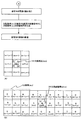
ここで、本発明における欠陥画素特定方法において欠陥画素の有無を特定する手段と、前記欠陥画素の座標を特定する手段を図2のフローチャートを用いて説明する。
【0027】
まず、半導体装置の画素部において、欠陥画素の有無を異なる色の少なくとも2枚のキャリブレーションシートを画素部が読み取ることにより特定する。ここで、本明細書で用いる色とは、一般に色相(単色光の波長に相当)、彩度(あざやかさ即ち白みを帯びていない度合)および明度(明るさ即ち光の強弱)の三要素によって規定されたものである。また、本明細書で用いる色とは、上述の三要素のうちのいずれか一つの要素のみ、または任意で選んだ2つの要素のみを示してもよい。本実施の形態では、ステップ1として、白色のキャリブレーションシートを読み取る。また、ステップ2として、黒色のキャリブレーションシートを読み取る。ステップ3として、ステップ1とステップ2から得られた画像信号の値の差を求める。
【0028】
なお、図2において、説明をわかりやすくするために、ステップ1〜ステップ3において、縦5×横5の画素部103を示す。画素102を表す四角形の中の数字は画像信号を示している。また、画素部103の周囲に示す数字は画素102の座標を示している。図2(A)は、白色のキャリブレーションシートを読み取った際の、それぞれの画素の画像信号を示している。また、図2(B)は、黒色のキャリブレーションシートを読み取った際のそれぞれの画素の画像信号を示している。ここで、ステップ1から得られた画像信号の値をS1(m、n)とする。(m、n)は座標を示しており、例えば、S1(1、1)は245である。また、ステップ2から得られた画像信号の値をS2(m、n)とする。例えば、S2(1、1)は50である。なお、本実施の形態においては、m、nはともに整数であり、1≦m≦5、1≦n≦5であるとする。
【0029】
また、本実施の形態では、ステップ1とステップ2に白色のキャリブレーションシートと黒色のキャリブレーションシートが用いられている。その理由は、ステップ1から得られる画像信号の値とステップ2から得られる画像信号の値との差から欠陥画素の有無を特定するため、得られる差が大きい方が好ましいからである。しかし、本発明では、ステップ1とステップ2の2回のキャリブレーションにより得られる同一画素での画像信号の値に差が生ずるならば、白色のキャリブレーションシートと黒色のキャリブレーションシートに限定されず、どのような色のキャリブレーションシートを行ってもよい。
【0030】
また、本実施の形態では2枚のキャリブレーションシートを読み取ることにより欠陥画素の有無を特定したが、本発明では、異なる色の少なくとも2枚のキャリブレーションシートを読み取ることにより欠陥画素の有無を特定すればよいため、枚数は2枚に限定されない。但し、2枚以上のキャリブレーションシートを読み取る場合は、複数枚のうちの任意の2枚のキャリブレーションシートを読み取ることにより得られた画像信号の差を複数個求めるようにするとよい。そして、得られた差の値により、欠陥画素を特定するとよい。
【0031】
次に、ステップ3として、それぞれの画素のステップ1により得られた画像信号の値と、それぞれの画素のステップ2により得られた画像信号の値との差を求める。図2(C)の画素102を表す四角形の中の数字は、その差を示している。ここで、ステップ1とステップ2により得られた差の値をS3(m、n)とする。例えば、S3(1、1)は、195である。
【0032】
次にステップ4として、それぞれの画素の画像信号の差の平均値を求める。はじめに、画素部103の画素のS3(m、n)の値の和を求め、求めた和を画素数(本実施の形態では25)で割る。ここで、ステップ4で求められる平均値はS4(Ave)とする。図2に示す画素部103の場合は、S4(Ave)は193.8となる。
【0033】
そしてステップ5では、ステップ4で得られたS4(Ave)の値193.8とそれぞれの画素の値S3(m、n)を比べる。以下の(式1)で表されるように、それぞれの画素の値S3(m、n)が、S4(Ave)の値193.8と比べて、80%〜120%以内の場合は欠陥のない画素とする。また、以下の(式2)と(式3)で表されるように、画素102の差の値が、平均値193.8に比べて80%以下または120%以上の場合は欠陥画素とする。
【0034】
【式1】
0.8<{S3(m、n)}/{S4(Ave)}<1.2
【0035】
【式2】
0.8>{S3(m、n)}/{S4(Ave)}
【0036】
【式3】
1.2<{S3(m、n)}/{S4(Ave)}
【0037】
そうすると、図2(A)〜図2(C)で示す画素部103の場合は、画素(2、3)は欠陥画素と特定される。そこで、同時に欠陥画素座標メモリに、欠陥画素の座標(2、3)が記憶される。
【0038】
なお、本実施の形態では、ステップ3において、ステップ1とステップ2より得られたそれぞれの画素の画像信号の値の差を求めたが、本発明はこれに限定されない。例えば、ステップ1とステップ2より得られたそれぞれの画素の画像信号の値の和を求めてもよいし、それぞれの画素の画像信号の比率、またはそれぞれの画像信号の積を求めてもよい。
【0039】
また、ステップ4において、平均値を計算したが、本発明はこれに限定されず、ステップ4では最大値を求めてもよいし、ヒストグラム上で最多値を求めてもよい。また、S4(Ave)の値を、使用者が自分で入力してもよい。
【0040】
なお、本実施の形態では、ステップ5において、それぞれの画素の値S3(m、n)が、S4(Ave)の値に比べて80%〜120%以内の画素は欠陥のない画素をしたが、本発明はこれに限定されない。ステップ4で求めた値に比べて、どの程度の違いがあれば欠陥画素とするかどうかは使用者が適宜決めることが可能である。また、統計学に基づく公知の方法で、分散や、標準偏差を用いて欠陥画素を特定してもよい。
【0041】
また、欠陥画素の座標を特定する手段としてのキャリブレーションは、半導体装置を初めて使用する際に行われるとよい。そして、欠陥画素の座標が一度特定されると、半導体装置が有する欠陥画素座標メモリにはその座標が記憶されることになる。そのため、再度キャリブレーションを行う必要はない。そして欠陥画素の座標が欠陥画素座標メモリに記憶されている場合は、図2および図3に示すフローチャートにおいて、Aで示す箇所から始めて、キャリブレーションは行わず、被写体の画像の読み取りから始めればよい。
【0042】
(実施の形態2)
本実施の形態では、欠陥画素の画像信号を生成する手段を図3を用いて説明する。
【0043】
図3を参照する。欠陥画素101の座標が特定され、欠陥画素座標メモリに座標が記憶されると、その欠陥画素101の画像信号は、欠陥画素と隣接している画素の画像信号から生成される。
【0044】
図3(A)は、半導体装置がモノクロで被写体の情報を読み取り、該被写体の画像をモノクロで表示する場合を示している。欠陥画素101の座標を(m、n)とすると、欠陥画素101に隣接している画素(m、n±1)、画素(m±1、n±1)、画素(m±1、n)のあわせて8個の画素における画像信号から欠陥画素の画像信号を生成する。より詳細には、欠陥画素101に隣接している画素(m、n±1)、画素(m±1、n±1)、画素(m±1、n)の画像信号の平均値を求めて、該平均値を欠陥画素101の画像信号とする。
【0045】
なお、図3(A)では、画素(m、n±1)、画素(m±1、n±1)、画素(m±1、n)のあわせて8個の画素から欠陥画素101(m、n)の画像信号を生成したが、本発明はこれに限定されない。例えば、上述した8個の画素に、画素(m±2、n±2)を加えて、合わせて12個の画素の画像信号の平均値をとってもよい。また、欠陥画素101の両隣にある画素(m±1、n)の2個の画素の平均値、あるいは欠陥画素101の上下にある画素(m、n±1)の平均値をとるようにしてもよい。また、欠陥画素101の画像信号を、欠陥画素101に隣接する画素(m、n±1)、画素(m±1、n±1)、画素(m±1、n)の8個の画素の内の任意の1個の画素の画像信号と同じにしてもよい。すなわち、欠陥画素に隣接するどこの画素の画像信号の平均値を欠陥画素の画像信号とするかは使用者が適宜決めることができる。
【0046】
また、欠陥画素が画素配列の端にある場合は、欠陥画素に隣接する画素の画像信号のみを用いて、欠陥画素の画像信号を生成してもよい。また、半導体装置が第一の欠陥画素と第二の欠陥画素を有しており、第一の欠陥画素と第二の欠陥画素が隣接している場合は、第一の欠陥画素に隣接している画素の内、第二の欠陥画素を除いた画素の画像信号から第一の欠陥画素の画像信号を生成してもよい。
【0047】
図3(B)は、半導体装置がカラーで被写体の情報を読み取り、該被写体の画像をカラーで表示する場合を示している。被写体の画像をカラーで読み取る方法としては、大まかに二つの方法がある。一つ目の方法は、それぞれの画素に一つの光電変換素子を設け、光源を赤(R)と緑(G)と青(B)の三回それぞれ切り替えて、被写体を三回読み取る方法である。二つ目の方法は、画素に赤(R)と緑(G)と青(B)のカラーフィルタを設け、光源を白色光にして、被写体を1回読み取る方法である。また、画素にカラーフィルタを設ける場合は、1つの画素に1色のカラーフィルタを設け、隣接する画素から異なる色の情報を得る場合と、1つの画素を3つの副画素に分けて、赤(R)と緑(G)と青(B)のカラーフィルタを設ける場合とがある。本実施の形態では、後者の場合について述べる。
【0048】
102は画素を示し、副画素R(m、n)と、副画素G(m、n)と、副画素B(m、n)を有する。欠陥副画素301の座標を(m、n)とすると、欠陥副画素301の周囲の副画素G(m、n±1)、副画素G(m±1、n±1)、副画素G(m±1、n)のあわせて8個の副画素における画像信号から欠陥副画素の画像信号を生成する。より詳細には、欠陥副画素301の周囲の副画素G(m、n±1)、副画素G(m±1、n±1)、副画素G(m±1、n)の画像信号の平均値を求めて、該平均値を欠陥副画素301の画像信号とする。
【0049】
なお、図3(B)では、副画素G(m、n±1)、副画素G(m±1、n±1)、副画素G(m±1、n)のあわせて8個の画素から欠陥副画素301(m、n)の画像信号を生成したが、本発明はこれに限定されない。例えば、上述した8個の画素に、画素G(m±2、n±2)を加えて、合わせて12個の画素の画像信号の平均値をとってもよい。また、副画素G(m±1、n)の2個の画素の平均値をとるようにしてもよい。すなわち、欠陥画素に隣接するどこの画素の画像信号の平均値を欠陥画素の画像信号とするかは使用者が適宜決めることができる。なお、本発明を用いた被写体の画像の修復は、一旦、被写体の全画面分のデータを読み取ってから行ってもよい。また、一行ずつまたは一画素ずつ被写体の情報を読み取りながら、被写体の画像を読み取った箇所の、被写体の画像を修復してもよい。
【0050】
なお、本発明は、実施の形態1と自由に組み合わせることが可能である。
【0051】
(実施の形態3)
本実施の形態では、光電変換素子を有する画素が複数設けられた画素部と、該画素部により読み取られた被写体の画像を表示する表示装置との関係について図4を用いて説明する。
【0052】
図4で示す画素部200には、読み取り機能を有する光電変換素子が設けられている。画素部200により読み取られた被写体の情報は、欠陥画素修復システムに出力される。なお本実施の形態では、欠陥画素特定システムと画像補正システムとを会わせて欠陥画素修復システムとよぶ。
【0053】
欠陥画素修復システムはCPU202と、画像信号修復回路203と、欠陥画素座標メモリ204とを有している。また、本発明の欠陥画素修復システムは、キャリブレーションにより、画素部において欠陥画素の有無を特定し、かつ前記欠陥画素の座標を特定する手段を有する。また、欠陥画素の画像信号を、欠陥画素に隣接する画素の画像信号から生成する手段を有することを特徴とする。
【0054】
欠陥画素座標メモリ204は、欠陥画素の座標が特定されると、該欠陥画素の座標が記憶される。また、画像信号修復回路203では、該欠陥画素に隣接する画素の画像信号から欠陥画素の画像信号を生成する。より詳細には、欠陥画素に隣接している画素の画像信号の平均値を求めて、該平均値を欠陥画素の画像信号とする。
【0055】
コントロール回路205は、欠陥画素修復システムにより生成された欠陥画素の画像信号および欠陥画素以外の画像信号を、表示部206に出力する。そして、表示部206では、画素部200で読み取られた被写体の画像を表示する。
【0056】
なお、本発明はイメージセンサ機能を有する全ての半導体装置に有効である。例えば、CCD型やCMOS型のイメージセンサ機能を有する半導体装置にも本発明は有効であるし、その他のすべてのイメージセンサ機能を有する半導体装置に本発明は有効である。また、ラインセンサおよびエリアセンサにも本発明は有効である。また、本発明を用いる半導体装置は、モノクロの画像を読み取る半導体装置でも、カラーの画像を読み取る半導体装置でもよい。また、単結晶(SOIやバルク)基板上に形成された場合や薄膜トランジスタを有する半導体装置にも有効である。
【0057】
スキャナなどの読み取り機能のみを有する半導体装置の場合は、任意の表示装置に画像を表示する際に、本発明を用いると、欠陥画素が修復されたように見せることが可能である。例えば、スキャナで読み取った被写体の情報を、任意のディスプレイに表示する場合においては、図4で示す画素部200と表示部206が異なっている。
【0058】
また、光電変換素子と発光素子を一画素とする半導体装置の場合は、被写体の情報の読み取りと、該被写体の表示を同じ画素で行う。このような半導体装置は、図4で示す画素部200と表示部206が同じである。
【0059】
なお、本発明は、実施の形態1、2と自由に組み合わせることが可能である。
【0060】
【実施例】
(実施例1)
本実施例では、本発明を適用することが可能な半導体装置の一例を説明する。
【0061】
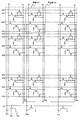
図5は、パッシブ型の半導体装置の画素部の回路図を示す。画素部103はセンサ選択信号線(SG1〜SGy)、センサ用信号出力線(SS1〜SSx)、センサ用電源線(VB1〜VBx)を有している。
【0062】
画素部103は複数の画素102を有している。画素102は、フォトダイオード111と、センサ選択用トランジスタ112と、センサ選択信号線(SG1〜SGy)のいずれか1つと、センサ用信号出力線(SS1〜SSx)のいずれか1つを有している。
【0063】
フォトダイオード111のPチャネル側端子は電源基準線121に接続されている。センサ選択用トランジスタ112のソース領域またはドレイン領域には、一方にはフォトダイオード111のNチャネル側端子が接続されており、もう一方にはセンサ用信号出力線(SS1〜SSx)が接続されている。センサ選択用トランジスタ112のゲート電極には、センサ選択信号線(SG1〜SGy)が接続されている。
【0064】
なお、本実施例は、実施の形態と自由に組み合わせることが可能である。
(実施例2)
本実施例では、実施例1とは異なる半導体装置の例について説明する。
【0065】
図6は、アクティブ型の半導体装置の画素部の回路図を示す。画素部103はセンサ選択信号線(SG1〜SGy)、センサリセット信号線(SR1〜SRy)、センサ用信号出力線(SS1〜SSx)、センサ用電源線(VB1〜VBx)を有している。
【0066】
画素部103は複数の画素102を有している。画素102は、フォトダイオード111と、センサ選択用トランジスタ112と、増幅用トランジスタ113と、センサリセット用トランジスタ114と、センサ選択信号線(SG1〜SGy)のいずれか1つと、センサリセット信号線(SR1〜SRy)のいずれか1つと、センサ用信号出力線(SS1〜SSx)のいずれか1つと、センサ用電源線(VB1〜VBx)のいずれか1つを有している。
【0067】
フォトダイオード111のPチャネル側端子は電源基準線121に接続され、Nチャネル側端子は、増幅用トランジスタ113のゲート電極に接続されている。
【0068】
増幅用トランジスタ113のドレイン領域とソース領域は、一方はセンサ用電源線(VB1〜VBx)に接続されており、もう一方はセンサ選択用トランジスタ112のドレイン領域に接続されている。増幅用トランジスタ113は、バイアス用トランジスタ120とソースフォロワ回路を形成する。そのため、増幅用トランジスタ113とバイアス用トランジスタ120の極性は同じである方がよい。
【0069】
センサ選択用トランジスタ112のゲート電極には、センサ選択信号線(SG1〜SGy)が接続され、センサ選択用トランジスタ112のソース領域には、センサ用信号出力線(SS1〜SSx)が接続されている。
【0070】
センサリセット用トランジスタ114のゲート電極は、センサリセット信号線(SR1〜SRy)に接続されている。センサリセット用トランジスタ114のソース領域とドレイン領域は、一方はセンサ用電源線(VB1〜VBx)に接続されており、もう一方は増幅用トランジスタ111のゲート電極に接続されている。
【0071】
バイアス用トランジスタ120のソース領域およびドレイン領域は、一方はセンサ用信号出力線(SS1〜SSx)に接続されており、もう一方は電源線122に接続されている。またバイアス用トランジスタ120のゲート電極は、バイアス用信号線(BS)に接続されている。
【0072】
実施例1および実施例2では、MOS型の半導体装置について説明したが、本発明は、CCD型の半導体装置にも適用することができる。なお、本実施例は、実施の形態および実施例1と自由に組み合わせることが可能である。
【0073】
(実施例3)
本実施例では、実施例1および実施例2とは異なる例について説明する。発光素子と光電変換素子を一画素中に用いた半導体装置について、図7および図8を用いて説明する。
【0074】
画素部103はソース信号線(S1〜Sx)、電源供給線(V1〜Vx)、選択信号線(EG1〜EGy)、リセット信号線(ER1〜ERy)、センサ選択信号線(SG1〜SGy)、センサリセット信号線(SR1〜SRy)、センサ用信号出力線(SS1〜SSx)、センサ用電源線(VB1〜VBx)を有している。
【0075】
画素部103は複数の画素102を有している。画素102は、ソース信号線(S1〜Sx)のいずれか1つと、電源供給線(V1〜Vx)のいずれか1つと、選択信号線(EG1〜EGy)のいずれか1つと、リセット信号線(ER1〜ERy)のいずれか1つと、センサ選択信号線(SG1〜SGy)のいずれか1つと、センサリセット信号線(SR1〜SRy)のいずれか1つと、センサ用信号出力線(SS1〜SSx)のいずれか1つと、センサ用電源線(VB1〜VBx)のいずれか1つを有している。また、画素102は、選択用トランジスタ116と、駆動用トランジスタ119と、リセット用トランジスタ117と、センサ選択用トランジスタ112と、増幅用トランジスタ113と、センサリセット用トランジスタ114とを有している。
【0076】
バイアス用トランジスタ120のソース領域およびドレイン領域は、一方はセンサ用信号出力線(SS1〜SSx)に接続されており、もう一方は電源線122に接続されている。またバイアス用トランジスタ120のゲート電極は、バイアス用信号線(BS)に接続されている。
【0077】
図8には、図7で示した画素部におけるi行目j列目の画素(i、j)を示す。
【0078】
フォトダイオード111は、nチャネル型端子、pチャネル型端子、およびnチャネル型端子とpチャネル型端子の間に設けられている光電変換層を有している。pチャネル型端子、nチャネル型端子の一方は、電源基準線121に接続されており、もう一方は増幅用トランジスタ113のゲート電極に接続されている。
【0079】
センサ選択用トランジスタ112のゲート電極はセンサ選択信号線(SGj)に接続されている。そしてセンサ選択用トランジスタ112のソース領域とドレイン領域は、一方は増幅用トランジスタ113のソース領域に接続されており、もう一方はセンサ用信号出力線(SSi)に接続されている。センサ選択用トランジスタ112は、フォトダイオード111の信号を出力するときのスイッチング素子として機能するトランジスタである。
【0080】
増幅用トランジスタ113のドレイン領域はセンサ用電源線(VBi)に接続されている。そして増幅用トランジスタ113のソース領域はセンサ選択用トランジスタ112のソース領域又はドレイン領域に接続されている。増幅用トランジスタ113は、バイアス用トランジスタ120とソースフォロワ回路を形成する。そのため、増幅用トランジスタ113とバイアス用トランジスタ120の極性は同じである方がよい。
【0081】
センサリセット用トランジスタ114のゲート電極は、センサリセット信号線(SRj)に接続されている。センサリセット用トランジスタ114のソース領域とドレイン領域は、一方はセンサ用電源線(VBi)に接続されており、もう一方は、フォトダイオード111及び増幅用トランジスタ113のゲート電極に接続されている。センサリセット用トランジスタ114は、フォトダイオード111を初期化するための素子として機能するトランジスタである。
【0082】
発光素子115は陽極と陰極と、陽極と陰極との間に設けられた有機化合物層とからなる。陽極が駆動用トランジスタ116のソース領域またはドレイン領域と接続している場合、陽極が画素電極となり、また陰極が対向電極となる。逆に陰極が駆動用トランジスタ116のソース領域またはドレイン領域と接続している場合、陰極が画素電極となり、陽極が対向電極となる。
【0083】
選択用トランジスタ116のゲート電極は選択信号線(EGj)に接続されている。そして選択用トランジスタ116のソース領域とドレイン領域は、一方がソース信号線(Si)に、もう一方が駆動用トランジスタ116のゲート電極に接続されている。選択用トランジスタ116は、画素(i、j)に信号を書き込むときのスイッチング素子として機能するトランジスタである。
【0084】
駆動用トランジスタ116のソース領域とドレイン領域は、一方が電源供給線(Vi)に、もう一方が発光素子115に接続されている。コンデンサ118は駆動用トランジスタ116のゲート電極と電源供給線(Vi)に接続して設けられている。駆動用トランジスタ116は、発光素子115に供給する電流を制御するための素子(電流制御素子)として機能するトランジスタである。
【0085】
リセット用トランジスタ117のソース領域とドレイン領域は、一方は電源供給線(Vi)に接続され、もう一方は駆動用トランジスタ116のゲート電極に接続されている。リセット用トランジスタ117のゲート電極は、リセット信号線(ERj)に接続されている。リセット用トランジスタ117は、画素(i、j)に書き込まれた信号を消去(リセット)するための素子として機能するトランジスタである。
【0086】
本実施例の半導体装置は、光電変換素子と発光素子のそれぞれを制御するための複数のトランジスタが設けられている。光電変換素子により読み取られた被写体の情報は、同じ画素に設けられた発光素子により表示される。
【0087】
読み取る機能を有する光電変換素子、および該光電変換素子を制御するトランジスタに欠陥が存在する画素を本明細書では欠陥画素をよぶが、同じ画素に設けられている発光素子、および該発光素子を制御するトランジスタに欠陥が無ければ、本発明を適用することが可能である。
【0088】
なお、本実施例は、実施の形態および実施例1、2と自由に組み合わせることが可能である。
【0089】
(実施例4)
本実施例では、実施例2で説明したアクティブ型のCMOSセンサの半導体装置の基本的な動作について説明する。図16には、図6で示した画素部103におけるi行目j列目の画素(i、j)を示す。
【0090】
まず、センサリセット用トランジスタ114を導通状態にする。センサリセット用トランジスタ114を導通状態にすると、光電変換素子111のpチャネル型端子が電源基準線121に接続された状態になり、かつ、光電変換素子111のnチャネル型端子がセンサ用電源線(VBi)に電気的に接続された状態となる。この際、電源基準線121の電位は基準電位0Vであり、センサ用電源線(VBi)の電位は電源電位Vddである。そのため、光電変換素子111には、逆バイアス電圧が与えられる。なお、本明細書では、光電変換素子111のnチャネル型端子の電位が、センサ用電源線(VBi)の電位まで充電される動作をリセットと呼ぶことにする。
【0091】
次に、センサリセット用トランジスタ114を非導通状態にする。センサリセット用トランジスタ114を非導通状態にすると、光電変換素子111に光が照射されていた場合は、光電変換により、光電変換素子111に電荷が発生する。そのため、時間が経過するに従って、センサ用電源線(VBi)の電位と同じ電位が充電されていた光電変換素子111のnチャネル型端子の電位は、徐々に低くなってしまう。
【0092】
次に、ある一定時間経過した後、センサ選択用トランジスタ112を導通状態にする。センサ選択用トランジスタ112を導通状態にすると、光電変換素子111のnチャネル型端子の電位が増幅用トランジスタ113を通って、センサ信号出力線(SSi)へ出力される。
【0093】
但し、センサ信号出力線(SSi)に光電変換素子111のnチャネル型端子の電位が出力されている状態において、バイアス信号線(BS)には、電位が与えられている。つまり、バイアス用トランジスタ120には、電流が流れるようになっているため、増幅用トランジスタ113とバイアス用トランジスタ120は、ソースフォロワ回路として機能している。
【0094】
図16では、光電変換素子111のpチャネル型端子が接続されている配線、つまり、電源基準線121は、光電変換素子側電源線と呼ぶこともできる。また、光電変換素子側電源線の電位は、光電変換素子111の向きによって変わる。図16では、光電変換素子側電源線には、光電変換素子111のpチャネル型端子が接続されており、その電位は基準電位0Vである。そのため、図16では、光電変換素子側電源線を電源基準線と呼んでいる。
【0095】
同様に、図16では、センサリセット用トランジスタ114が接続されている配線、つまり、センサ用電源線(VBi)は、リセット側電源線と呼ぶこともできる。リセット側電源線の電位は、光電変換素子111の向きによって変わる。図16では、リセット側電源線には、センサリセット用トランジスタ114を介して、光電変換素子111のnチャネル側端子が接続されており、その電位は電源電位Vddである。そのため、図16では、リセット側電源線を電源線と呼んでいる。
【0096】
なお、光電変換素子111をリセットする動作は、光電変換素子111に逆バイアス電圧が与えられる動作と同じである。よって、光電変換素子111の向きによって、光電変換素子側電源線とリセット側電源線の電位の大小関係は変化する。
【0097】
次に、図17に基本的なソースフォロワ回路の例を示す。図17では、nチャネル型トランジスタを用いた場合について示すが、pチャネル型トランジスタを用いてソースフォロワ回路を構成することも出来る。
【0098】
増幅側電源線130には、電源電位Vddが与えられており、電源線122には、基準電位0Vが与えられている。増幅用トランジスタ113のドレイン領域は増幅側電源線130に接続され、増幅用トランジスタ113のソース領域はバイアス用トランジスタ120のドレイン領域に接続されている。バイアス用トランジスタ120のソース領域は、電源線122に接続されている。
【0099】
バイアス用トランジスタ120のゲート電極には、バイアス電位Vbが与えられ、バイアス用トランジスタ120には、バイアス電流Ibが流れている。バイアス用トランジスタ120は、定電流源として動作する。
【0100】
図17において、増幅用トランジスタ113のゲート電極が、入力端子131である。よって、増幅用トランジスタ113のゲート電極には、入力電位Vinが加えられる。また、増幅用トランジスタ113のソース領域が出力端子132である。よって、増幅用トランジスタ113のソース領域の電位が、出力電位Voutとなる。この際、ソースフォロワ回路の電位の入出力関係は、Vout=Vin−Vbとなる。
【0101】
なお、図17においては、センサ選択用トランジスタ112は、導通状態であることを想定し、省略されている。また光電変換素子111のnチャネル型端子の電位は、入力電位Vin(増幅用トランジスタ113のゲート電位、つまり入力端子131の電位)に対応する。センサ信号出力線(SSi)の電位は、出力電位Vout(増幅用トランジスタ113のソース電位、つまり出力端子132の電位)に対応する。センサ用電源線(VBi)は、増幅側電源線130に対応する。
【0102】
従って、図16において、光電変換素子111のnチャネル型端子の電位をVpdとし、バイアス信号線(BS)の電位、つまり、バイアス電位をVbとし、センサ信号出力線(SSi)の電位をVoutとする。また、電源基準線121と電源線122の電位を0Vとすると、Vout=Vpd−Vbとなる。よって、光電変換素子111のnチャネル型端子の電位Vpdが変化すると、Voutも変化することになり、Vpdの変化を信号として出力する。よって、光電変換素子111は、光強度を読み取ることが出来る。
【0103】
次に、画素102での信号のタイミングチャートを図18に示す。
【0104】
始めに、センサリセット信号線(SR1〜SRy)を制御し、センサリセット用トランジスタ114を導通状態にする。
【0105】
次に、光電変換素子111のnチャネル型端子の電位は、センサ用電源線(VBi)の電位である電源電位Vddにまで充電される。すなわち、画素102がリセットされる。それから、センサリセット信号線(SR1〜SRy)を制御し、センサリセット用トランジスタ114を非導通状態にする。
【0106】
その後、光電変換素子111に光が照射されていると、光強度に応じた電荷が光電変換素子111に発生する。そして、リセットにより充電された電荷が、徐々に放電され、光電変換素子111のnチャネル型端子の電位が低くなってくる。
【0107】
図16に示すように、光電変換素子111に明るい光が照射されている場合は、放電される量が多いため、光電変換素子111のnチャネル型端子の電位は低くなる。光電変換素子111に暗い光が照射されている場合は、放電される量が少なく、光電変換素子111のnチャネル型端子の電位は、明るい光が照射されている場合に比べると、あまり低くならない。
【0108】
そして、ある時点において、センサ選択用トランジスタ112を導通状態にして、光電変換素子111のnチャネル型端子の電位を信号として読み出す。この信号は、光電変換素子111に照射された光の強度に比例している。そして、再びセンサリセット用トランジスタ114を導通状態にして光電変換素子111をリセットし、上述の動作を繰り返していく。
【0109】
但し、非常に明るい光が照射された場合は、光電変換素子111の電荷の放電される量が非常に多いため、光電変換素子111のnチャネル型端子の電位は、非常に低下してしまう。しかし、光電変換素子111のnチャネル型端子の電位は、光電変換素子111のpチャネル型端子、つまり電源基準線121の電位より低くなることはない。
【0110】
また、非常に明るい光が照射された場合は、光電変換素子111のnチャネル型端子の電位が低くなってくるが、その電位が電源基準線121の電位まで低くなると、電位は変化しなくなる。このような状況を飽和と呼ぶ。飽和すると、光電変換素子111のnチャネル型端子の電位が変化しなくなってしまうため、正しい光強度に応じた信号を出力できない。よって、正常に動作させるためには、光電変換素子111が飽和しないようにして、動作させる必要がある。
【0111】
また、画素102がリセットされてから、信号を出力する時までの期間は、蓄積時間と呼ばれる。蓄積時間とは、イメージセンサの受光部に光を照射し、信号を蓄積している時間のことであり、露光時間ともよばれる。蓄積時間において、光電変換素子111は、光電変換素子111に照射された光によって生成される電荷を蓄積している。
【0112】
よって、蓄積時間が異なると、たとえ同じ光強度であっても、光によって生成される電荷の総量が異なるため、信号値も異なってしまう。例えば、強い光が光電変換素子111に照射された場合は、短い蓄積時間で飽和してしまう。また、弱い光が光電変換素子111に照射された場合であっても、蓄積時間が長いと、いずれは飽和状態に達する。つまり、信号は、光電変換素子111に照射される光の強さと蓄積時間との積によって決定する。
【0113】
なお、本実施例は、実施の形態および実施例1乃至実施例3と自由に組み合わせることが可能である。
【0114】
(実施例5)
本実施例では、半導体装置に黒色のキャリブレーションシートを読み取らせる動作と同様の動作をさせる半導体装置の駆動方法について説明する。
【0115】
本実施例では、アクティブ型のCMOSセンサの半導体装置において、センサリセット用トランジスタ114にリセット信号が印可された際に、光電変換素子111のnチャネル型端子の電位を読み出すことにする。
【0116】
センサリセット用トランジスタ114にリセット信号が印可された際に、読み出される光電変換素子111のnチャネル型端子の電位は、黒色のキャリブレーションシートの読み取りを行って、読み出される光電変換素子111の電位とほぼ同じである。つまり、センサリセット用トランジスタ114にリセット信号が印可された際に、光電変換素子111のnチャネル型端子の電位を読み出す動作は、黒色のキャリブレーションシートを読み取る動作と同じ動作をしていることになる。その理由を以下に述べる。
【0117】
黒色のキャリブレーションシートの読み取りを行った際、光電変換素子111に照射される光はほとんどない。つまり、光電変換素子111では、光電変換はほとんど行われず、光電変換素子111には、電荷は蓄積されない。そのため、黒のキャリブレーションシートの読み取りを行った際、光電変換素子111のnチャネル型端子の電位はセンサ用電源線(VB1〜VBx)の電位とほぼ同じ値となる。
【0118】
一方、センサリセット用トランジスタ114にリセット信号を印可した際にも、光電変換素子111のnチャネル型端子の電位は、センサ用電源線(VB1〜VBx)とほぼ同じ値にまで充電される。
【0119】
つまり、センサリセット用トランジスタ114にリセット信号を印可された際に、読み出される光電変換素子111の電位は、黒色のキャリブレーションシートの読み取りを行って、読み出される光電変換素子111の電位と、ほぼ同じ電位であることが分かる。
【0120】
なお、本実施例では、リセット信号を印可した際に読み取る被写体は、キャリブレーションシートを用いる必要はなく、どのような被写体でもよい。
【0121】
なお、イメージセンサ機能を有する半導体装置には、実際に被写体を読み取る際、リセット信号を印可した際の光電変換素子111の信号を読み取っている半導体装置がある。そのような半導体装置の場合は、リセット信号を印可した際の光電変換素子111の信号を用いればよい。
【0122】
以上は、アクティブ型のCMOSセンサの半導体装置について述べたが、以下にパッシブ型のCMOSセンサの半導体装置について述べる。
【0123】
パッシブ型の半導体装置の場合には、図19に示すように選択信号が印可された際に、光電変換素子111に蓄積された電荷を読み出す。そして、すぐに光電変換素子111の電位は、センサ用電源線(VB1〜VBx)の電位にまで充電される。
【0124】
本実施例では、光電変換素子111の電位が、センサ用電源線(VB1〜VBx)の電位にまで充電された際に、光電変換素子111に蓄積された電荷を読み出すことにする。そのためには、選択信号を印可した後、すぐに選択信号を再び印可して、蓄積時間を短くして、光電変換素子111の電位が、センサ用電源線(VB1〜VBx)の電位にまで充電された際の光電変換素子111の電位を読み出してもよい。また、選択信号を印可する時間を長くし、光電変換素子の電位がセンサ用電源線(VB1〜VBx)の電位にまで充電された際の、光電変換素子111の電位を読み出してもよい。このように蓄積時間を短くした場合の信号を読み出せばよい。
【0125】
以上は、MOS型の半導体装置について説明したが、本実施例は、CCD型の半導体装置など、イメージセンサ機能を有する全ての半導体装置に適用することができる。
【0126】
なお、本実施例の駆動方法は、本明細書の実施の形態で説明した図2のステップ2に相当する。つまり、白色のキャリブレーションを行うステップ1と、本実施例を組み合わせれば、欠陥画素の有無を特定し、かつ欠陥画素の座標を特定することができる。
【0127】
また、本実施例は、実施の形態および実施例1乃至実施例4と自由に組み合わせることが可能である。
【0128】
(実施例6)
本実施例では、半導体装置に白色のキャリブレーションシートを読み取らせる動作と同様の動作をさせる半導体装置の駆動方法について説明する。
【0129】
本実施例では、光電変換素子111の蓄積時間を長くすることにより、白色のキャリブレーションシートを読み取らせる動作と同じ動作をする半導体装置の駆動方法について説明する。以下に本発明が適用される具体的な光電変換素子111の蓄積時間の長さを説明する。
【0130】
光電変換素子111に流れる暗電流をIdとおく。暗電流Idとは、光電変換素子111に光が照射されていない状態においても、光電変換素子111に流れてしまう電流のことである。そして、光電変換素子111の容量をCとし、このときの光電変換素子111の蓄積時間をTとする。また、リセット信号を印可した際に光電変換素子の両端に加わる電圧の値をVpとする。そうすると、電荷Qは以下の(式4)と(式5)のように表される。
【式4】
Q=C×Vp
【0131】
【式5】
Q=Id×T
【0132】
また、(式4)と(式5)から、以下の(式6)が求められる。
【0133】
【式6】
T=(C×Vp)/Id
【0134】
本実施例では、蓄積時間が以下の(式7)を満たす場合に、光電変換素子111のnチャネル型端子の電位を読み出すことにする。
【0135】
【式7】
T>(C×Vp)/Id
【0136】
(式7)を満たす蓄積時間において、読み出される光電変換素子111のnチャネル型端子の電位は、白色のキャリブレーションシートの読み取りを行って、読み出される光電変換素子111の電位とほぼ同じである。つまり、(式7)を満たす蓄積時間において、光電変換素子111のnチャネル型端子の電位を読み出す動作は、白色のキャリブレーションシートを読み取る動作と同じ動作をしていることになる。理由を以下に述べる。
【0137】
白色のキャリブレーションシートの読み取りを行った際、光電変換素子111に照射される光は、非常に明るい光である。つまり、光電変換素子111では、光電変換はほぼ飽和状態にまで行われ、光電変換素子111に電荷が蓄積される。そのため、白色のキャリブレーションシートの読み取りを行った際、光電変換素子111のnチャネル型端子の電位はほとんど放電されている。
【0138】
(式7)を満たす蓄積時間においては、光電変換素子111のnチャネル型端子の電位を読み出す動作は、光電変換素子111のnチャネル型端子の電位がほとんど放電された状態であるため、白色のキャリブレーションシートを読み出す動作と同じである。
【0139】
なお、本実施例では、半導体装置が読み取る被写体は、キャリブレーションシートを用いる必要はなく、どのような被写体でもよい。
【0140】
なお、本実施例は、アクティブ型の半導体装置、パッシブ型の半導体装置のいずれも有効である。またCCD型の半導体装置にも有効である。
【0141】
なお、本実施例の駆動方法は、本明細書の実施の形態で説明した図2のステップ1に相当する。つまり、黒色のキャリブレーションを行うステップ2と、本実施例を組み合わせれば、欠陥画素の有無を特定し、かつ欠陥画素の座標を特定することができる。
【0142】
また、本実施例は、実施の形態および実施例1乃至実施例5と自由に組み合わせることが可能である。
【0143】
(実施例7)
本実施例では、本発明を用いて実際に得られた被写体の画像、および本発明のシステムのウインドウの画像を示す。なお本実施例で示すシステムは、windows98が搭載されたパソコンにインストールされたVisual Basic6.0(マイクロソフト社)を用いて作成された。
【0144】
図9は白のキャリブレーションを行い、得られた画像を示す。図9に示されるように、白のキャリブレーションを行うと、欠陥画素が黒色の点として示されている。図10は黒のキャリブレーションを行って得られた画像を示す。図10に示されるように、黒のキャリブレーションを行うと、欠陥画素が白色の点として示されている。図9と図10から、欠陥画素の場所が分かる。
【0145】
図11は、本発明を使用している際のパソコンの画面を示したものである。図11には、図9で示した白のキャリブレーションを行って得られた画像と該画像の画像信号を数字で表した表が示されている。また、図10で示した黒のキャリブレーションにより得られた画像と、該画像の画像信号を数字で表した表が示されている。
【0146】
図12は、本発明を用いていない半導体装置によって、読み取られた被写体の画像を示したものである。図13は、本発明を用いた半導体装置によって、読み取られた被写体の画像を示したものである。
【0147】
図12と図13を比べると、図12には、欠陥画素が黒色の点および白色の点で示されていることが分かる。しかし、図13では、欠陥画素の画像信号は、欠陥画素の周囲の信号で生成され、目立たなくなっており、見かけ上は欠陥画素が修復されている。
【0148】
なお、本実施例は、実施の形態および実施例1乃至実施例6と自由に組み合わせることが可能である。
【0149】
(実施例8)
本発明の半導体装置を用いた電子機器の実施例として、図14を用いて説明する。
【0150】
図14(A)は、ラインセンサを用いたハンドスキャナーである。CCD型(CMOS型)のイメージセンサ1001の上には、ロッドレンズアレイなどの光学系1002が設けられている。光学系1002は、被写体1004上の画像がイメージセンサ1001上に映し出されるようにするために用いられる。
【0151】
そして、LEDや蛍光灯などの光源1003は、被写体1004に光を照射できる位置に設けられている。そして、被写体1004の下部には、ガラス1005が設けられている。
【0152】
光源1003を出た光は、ガラス1005を介して被写体1004に入射する。被写体1004で反射した光は、ガラス1005を介して、光学系1002に入射する。光学系1002に入射した光は、イメージセンサ1001に入射し、そこで光電変換される。
【0153】
図14(B)は、1801は基板、1802は画素部、1803はタッチパネル、1804はタッチペンである。タッチパネル1803は透光性を有しており、画素部1802から発せられる光及び、画素部1802に入射する光を透過することができ、タッチパネル1803を通して被写体上の画像を読み込むことができる。また画素部1802に画像が表示されている場合にも、タッチパネル1803を通して、画素部1802上の画像を見ることが可能である。
【0154】
タッチペン1804がタッチパネル1803に触れると、タッチペン1804とタッチパネル1803とが接している部分の位置の情報を、電気信号として半導体装置に取り込むことができる。本実施例で用いられるタッチパネル1803及びタッチペン1804は、タッチパネル1803が透光性を有していて、なおかつタッチペン1804とタッチパネル1803とが接している部分の位置の情報を、電気信号として半導体装置に取り込むことができるものならば、公知のものを用いることができる。
【0155】
上記構成を有する本発明の半導体装置は、画像の情報を読み込んで、画素部1802に読み込んだ画像を表示し、取り込んだ画像にタッチペン1804で書き込みを行うことができる。そして本発明の半導体装置は、画像の読み込み、画像の表示、画像への書き込みを、全て画素部1802において行うことができる。よって半導体装置自体の大きさを抑え、なおかつ様々な機能を半導体装置に持たせることができる。
【0156】
図14(C)は、図14(B)とは異なる携帯型ハンドスキャナーであり、本体1901、画素部1902、上部カバー1903、外部接続ポート1904、操作スイッチ1905で構成されている。図14(D)は図14(C)と同じ携帯型ハンドスキャナーの上部カバー1903を閉じた図である。
【0157】
本発明の半導体装置は、読み込んだ画像の情報を画素部1902において表示することが可能であり、新たにディスプレイを半導体装置に設けなくとも、その場で読み込んだ画像を確認することができる。
【0158】
また画素部1902で読み込んだ画像信号を、外部接続ポート1904から携帯型ハンドスキャナーの外部に接続されている電子機器に送り、パソコンにおいて画像を補正、合成、編集等を行うことも可能である。
【0159】
なお、本実施例は、実施の形態および実施例1乃至実施例7と自由に組み合わせることが可能である。
【0160】
(実施例9)
また、本発明の半導体装置を用いた電子機器として、ビデオカメラ、デジタルスチルカメラ、ノート型パーソナルコンピュータ、携帯情報端末(モバイルコンピュータ、携帯電話、携帯型ゲーム機または電子書籍等)などが挙げられる。
【0161】
図15(A)はビデオカメラであり、本体2601、表示部2602、筐体2603、外部接続ポート2604、リモコン受信部2605、受像部2606、バッテリー2607、音声入力部2608、操作キー2609等を含む。本発明¥は表示部2602に用いることができる。
【0162】
図15(B)はモバイルコンピュータであり、本体2301、表示部2302、スイッチ2303、操作キー2304、赤外線ポート2305等を含む。本発明は表示部2302に用いることができる。
【0163】
図15(C)は携帯電話であり、本体2701、筐体2702、表示部2703、音声入力部2704、音声出力部2705、操作キー2706、外部接続ポート2707、アンテナ2708等を含む。本発明は表示部2703に用いることができる。
【0164】
以上の様に、本発明の適用範囲は極めて広く、あらゆる分野の電子機器に用いることが可能である。
【0165】
なお、本実施例は、実施の形態および実施例1乃至実施例8と自由に組み合わせることが可能である。
【0166】
【発明の効果】
本発明を用いることにより、欠陥画素がある半導体装置においても、欠陥画素のない半導体装置と同等のイメージセンサ機能を実現することができる。その結果、製品歩留まりを向上させることができる。
【0167】
【図面の簡単な説明】
【図1】 本発明を説明する図。
【図2】 本発明の概念を示す模式図。
【図3】 本発明の概念を示す模式図。
【図4】 本発明の概念を示す模式図。
【図5】 本発明を適用することができる半導体装置の回路図。
【図6】 本発明を適用することができる半導体装置の回路図。
【図7】 本発明を適用することができる半導体装置の回路図。
【図8】 本発明を適用することができる半導体装置の画素の回路図。
【図9】 本発明の使用形態を示す図。
【図10】 本発明の使用形態を示す図。
【図11】 本発明の使用形態を示す図。
【図12】 本発明の使用形態を示す図。
【図13】 本発明の使用形態を示す図。
【図14】 本発明を適用可能な電子機器の図。
【図15】 本発明を適用可能な電子機器の図。
【図16】 本発明を適用することができる半導体装置の画素の回路図。
【図17】 本発明を適用することができる半導体装置の画素の回路図。
【図18】 本発明を適用することができる半導体装置の動作形態を示す図。
【図19】 本発明を適用することができる半導体装置の動作形態を示す図。[0001]
BACKGROUND OF THE INVENTION
The present invention relates to a defective pixel specifying method and a defective pixel specifying system for a semiconductor device having an image sensor function. The present invention also relates to an image correction method and an image correction system for an image read by a semiconductor device having an image sensor function.
[0002]
[Prior art]
In recent years, various sensors have been developed and put into practical use as the technology advances. Semiconductor devices provided with an image sensor function have come to be used in order to incorporate character / graphic information on a paper surface into a personal computer.
[0003]
Such semiconductor devices include digital still cameras, scanners, copiers, and the like. The digital still camera is used as an alternative to a conventional silver salt camera, and is provided with an area sensor in which pixels are arranged two-dimensionally. Scanners, copiers, and the like are used as means for reading character / graphic information on paper, and are provided with a line sensor in which pixels are arranged one-dimensionally.
[0004]
Scanners can be broadly classified into three types: (1) sheet feed type, (2) flat bed type, and (3) pen type (handy type). (1) The sheet feed type is a method in which an image sensor unit of a scanner is fixed and an original is moved by paper feeding and read. (2) The flat bed type is a method in which an original is fixed on a glass and an image sensor unit is moved under the glass to read. (3) The pen type (handy type) is a method in which the user moves the image sensor unit on a document and reads it.
[0005]
Each of the above three scanners employs an optical system. (2) A flatbed scanner often employs a reduction optical system in order to accurately read an image. Since the lens used in the reduction optical system has a long focal length, the distance between the subject and the image sensor unit becomes long, and the semiconductor device becomes large.
[0006]
In (1) sheet feed type and (3) pen type (handy type), it is necessary to reduce the size of the apparatus so that it can be carried and carried. Therefore, a contact type optical system is often adopted as the optical system. The contact optical system is used by arranging a rod lens array between an image sensor unit and a subject. The rod lens array is a bundle of a plurality of distributed refractive index rod-shaped lenses. Further, since the rod lens array forms an image on a one-to-one basis and can shorten the focal length, the distance between the subject and the image sensor unit can be shortened.
[0007]
When the scanner is purchased as a product, it is recommended that the user perform calibration before reading the subject.
[0008]
There are two reasons for performing calibration.
[0009]
The first reason is that the light emitted to the subject from the light source used in the scanner is not uniformly emitted. As described above, the scanner uses a lens such as a reduction optical system or a rod lens array. The light from the light source provided in the scanner is irradiated to the subject through these lenses. For this reason, the intensity of light applied to the subject may vary depending on the location.
[0010]
The second reason is to correct variation in characteristics of each pixel of the image sensor. The variation means that the signal value read by each pixel is slightly different when the subject having the same information on the paper surface is read. If there is variation for each pixel, the signal value output from the photoelectric conversion element is different even if the subject is irradiated with light of the same intensity from the light source. In many cases, the variation in characteristics from pixel to pixel does not change with time.
[0011]
Therefore, after purchasing a scanner, it is recommended to perform calibration before reading the subject. Actually, there are cases where a calibration sheet having the same size as the effective reading range of the scanner is enclosed in a commercially available scanner. The calibration sheet is a white sheet made of plastic. In this specification, the calibration sheet refers to a sheet whose reading range of the semiconductor device has the same brightness when used for calibration. Preferably, a sheet made of plastic that is not permeable and is strong is preferable. Further, a flat sheet having no holes or dents is preferable.
[0012]
When the calibration sheet is read, all the information read for each pixel should be the same. However, the actually read information may be different for the two reasons described above. For this reason, information obtained when a white sheet is read is stored in a program provided in a scanner or the like. Then, when actually reading the subject, correction is performed based on the information. Note that once the calibration is performed, the information can be saved, so that further calibration is not necessary.
[0013]
Further, it is recommended to perform calibration for a semiconductor device having an image sensor function. The calibration method differs depending on the semiconductor device. For example, a scanner performs calibration using a calibration sheet. However, in the case of a digital still camera, calibration software is attached. Since a digital still camera takes an image through a lens, the image may be slightly distorted. Therefore, calibration is performed and distortion is measured. Then, by calculating a correction value of the distortion of the lens and giving the correction value to the program of the digital still camera, the influence of the distortion can be reduced to the minimum.
[0014]
[Problems to be solved by the invention]
A semiconductor device having an image sensor function is provided with a pixel portion having a plurality of pixels. The plurality of pixels are each provided with a photoelectric conversion element and one or a plurality of transistors for controlling the photoelectric conversion element.
[0015]
As the photoelectric conversion element, a PN type photodiode is often used. In addition, there are a PIN type photodiode, an avalanche type diode, an npn buried type diode, a Schottky type diode, a phototransistor, and the like. In addition, there are X-ray photoconductors and infrared sensors. The semiconductor device of the present invention can be applied to all photoelectric conversion elements.
[0016]
Semiconductor devices having an image sensor function are roughly classified into a CCD type and a CMOS type. A CMOS type semiconductor device is called a passive type without an amplifying transistor, and an active type with an amplifying transistor. The amplifying transistor has a function of amplifying the image signal of the subject read by the photoelectric conversion element.
[0017]
In an active semiconductor device, a sensor selection transistor and the like are provided in addition to the amplifying transistor described above, and the number of elements provided in one pixel increases. The more elements provided in one pixel, the lower the yield when forming a semiconductor device.
[0018]
As a result, it becomes very difficult to form a semiconductor device having no defective pixels. When forming a semiconductor device, a photoelectric conversion element provided in the pixel or a plurality of photoelectric conversion elements for controlling the photoelectric conversion element Any one of the transistors may not be formed normally. Since such pixels cannot operate normally, the image of the subject cannot be read correctly. In this specification, such a pixel is referred to as a defective pixel. In a semiconductor device having a defective pixel, when a read image of a subject is displayed, a portion where the defective pixel exists is often displayed as a white point or a black point. Therefore, the image of the defective pixel portion is conspicuous, and the read image of the subject is not accurately displayed.
[0019]
The present invention has been made in view of the above-described problems, and provides an image correction method that makes a defect of a defective pixel inconspicuous when a read image is displayed in a semiconductor device having the defective pixel. is there.
[0020]
[Means for Solving the Problems]
Please refer to FIG. FIG. 1A illustrates, as an example, an image of a uniform halftone object read by a semiconductor device provided with pixels including photoelectric conversion elements, which is displayed on a
[0021]
Therefore, the defective pixel identification method and the image correction method of the present invention are used. The defective pixel specifying method of the present invention includes a first step of obtaining a plurality of image signals by the photoelectric conversion element for each of the pixels,
A second step of determining, for each pixel, a first difference or a first ratio of the plurality of image signals obtained by the first step;
A third step of obtaining any one of the maximum value, the average value, or the maximum value of the first difference or the first ratio in the pixel portion;
A second difference or first difference between the first difference or the first ratio obtained by the second step and the maximum value, the average value, or the maximum value obtained by the third step. And a fourth step of identifying the defective pixel by obtaining a ratio of 2 for each of the pixels.
The image correction method of the present invention includes a first step in which an image signal read by the photoelectric conversion element is input,
A second step of obtaining an average value of image signals of pixels adjacent to the defective pixel, and a third step of setting the average value as an image signal of the defective pixel;
And a fourth step of outputting an image signal of the defective pixel to a display device that displays an image read by the photoelectric conversion element.
[0022]
FIG. 1C shows an image of a subject read by a semiconductor device having a defective pixel specifying system and an image correction system of the present invention. As shown in FIG. 1D, the image signal of the pixel (m, n) is generated from the image signal of the pixel adjacent to the defective pixel and restored from 55 to 200. As a result, the defective pixel 101 is not noticeable as compared with FIG.
[0023]
By using the present invention, a defective pixel can be made inconspicuous in a semiconductor device having a defective pixel. In addition, it seems that the defective pixel is repaired.
[0024]
The present invention is effective for all semiconductor devices having an image sensor function. For example, the present invention is effective for a semiconductor device having a CCD type or CMOS type image sensor function, and the present invention is effective for any other semiconductor device having an image sensor function. The present invention is also effective for line sensors and area sensors. The semiconductor device using the present invention may be a semiconductor device that reads a monochrome image or a semiconductor device that reads a color image. Further, it is also effective for a semiconductor device having a thin film transistor when formed over a single crystal (SOI or bulk) substrate.
[0025]
In the case of a semiconductor device having only a reading function such as a scanner, when an image is displayed on an arbitrary display device, the present invention can be used to make it appear that a defective pixel is repaired. Further, it is also effective for a semiconductor device in which a photoelectric conversion element having a reading function and a display element for displaying an image read by the photoelectric conversion element are used as one pixel. In the case of such a semiconductor device, when the read information of the subject is displayed on the display element, the present invention can be used to make it appear that the defective pixel is repaired.
[0026]
DETAILED DESCRIPTION OF THE INVENTION
(Embodiment 1)
Here, means for specifying the presence or absence of a defective pixel and means for specifying the coordinates of the defective pixel in the defective pixel specifying method of the present invention will be described with reference to the flowchart of FIG.
[0027]
First, in the pixel portion of the semiconductor device, the pixel portion identifies the presence or absence of defective pixels by reading at least two calibration sheets of different colors. Here, the color used in the present specification generally means three elements of hue (corresponding to the wavelength of monochromatic light), saturation (brightness, that is, no whiteness), and lightness (brightness, that is, intensity of light) It is specified by. In addition, the color used in the present specification may indicate only one of the above three elements or only two elements selected arbitrarily. In the present embodiment, as
[0028]
In FIG. 2, in order to make the explanation easy to understand, the
[0029]
In the present embodiment, a white calibration sheet and a black calibration sheet are used in
[0030]
In this embodiment, the presence or absence of defective pixels is specified by reading two calibration sheets. However, in the present invention, the presence or absence of defective pixels is specified by reading at least two calibration sheets of different colors. Therefore, the number of sheets is not limited to two. However, when reading two or more calibration sheets, it is preferable to obtain a plurality of differences in image signals obtained by reading any two of the plurality of calibration sheets. And it is good to specify a defective pixel by the value of the obtained difference.
[0031]
Next, as
[0032]
Next, as
[0033]
In
[0034]
[Formula 1]
0.8 <{S3 (m, n)} / {S4 (Ave)} <1.2
[0035]
[Formula 2]
0.8> {S3 (m, n)} / {S4 (Ave)}
[0036]
[Formula 3]
1.2 <{S3 (m, n)} / {S4 (Ave)}
[0037]
Then, in the case of the
[0038]
In the present embodiment, the difference between the image signal values of the respective pixels obtained in
[0039]
Moreover, although the average value was calculated in
[0040]
In the present embodiment, in
[0041]
Further, calibration as a means for specifying the coordinates of defective pixels may be performed when the semiconductor device is used for the first time. Once the coordinates of the defective pixel are specified, the coordinates are stored in the defective pixel coordinate memory of the semiconductor device. Therefore, it is not necessary to perform calibration again. If the coordinates of the defective pixel are stored in the defective pixel coordinate memory, it is only necessary to start from the position indicated by A in the flowcharts shown in FIGS. 2 and 3 and start reading the image of the subject without performing calibration. .
[0042]
(Embodiment 2)
In this embodiment, means for generating an image signal of a defective pixel will be described with reference to FIG.
[0043]
Please refer to FIG. When the coordinates of the defective pixel 101 are specified and the coordinates are stored in the defective pixel coordinate memory, the image signal of the defective pixel 101 is generated from the image signal of the pixel adjacent to the defective pixel.
[0044]
FIG. 3A illustrates a case where the semiconductor device reads information on a subject in monochrome and displays an image of the subject in monochrome. If the coordinates of the defective pixel 101 are (m, n), the pixel (m, n ± 1), pixel (m ± 1, n ± 1), pixel (m ± 1, n) adjacent to the defective pixel 101 In addition, an image signal of a defective pixel is generated from the image signals of 8 pixels. More specifically, an average value of image signals of pixels (m, n ± 1), pixels (m ± 1, n ± 1), and pixels (m ± 1, n) adjacent to the defective pixel 101 is obtained. The average value is used as the image signal of the defective pixel 101.
[0045]
In FIG. 3A, the defective pixel 101 (m) is composed of eight pixels including the pixel (m, n ± 1), pixel (m ± 1, n ± 1), and pixel (m ± 1, n). , N) are generated, but the present invention is not limited to this. For example, pixels (m ± 2, n ± 2) may be added to the eight pixels described above, and an average value of image signals of twelve pixels may be taken. Further, an average value of two pixels (m ± 1, n) adjacent to the defective pixel 101 or an average value of pixels (m, n ± 1) above and below the defective pixel 101 is taken. Also good. In addition, the image signal of the defective pixel 101 is obtained from eight pixels of the pixel (m, n ± 1), the pixel (m ± 1, n ± 1), and the pixel (m ± 1, n) adjacent to the defective pixel 101. It may be the same as the image signal of any one of the pixels. That is, the user can appropriately determine which pixel adjacent to the defective pixel is the average value of the image signal of the defective pixel.
[0046]
In addition, when the defective pixel is at the end of the pixel array, the image signal of the defective pixel may be generated using only the image signal of the pixel adjacent to the defective pixel. In addition, when the semiconductor device has the first defective pixel and the second defective pixel, and the first defective pixel and the second defective pixel are adjacent to each other, the semiconductor device is adjacent to the first defective pixel. The image signal of the first defective pixel may be generated from the image signal of the pixel excluding the second defective pixel among the existing pixels.
[0047]
FIG. 3B illustrates a case where the semiconductor device reads information on a subject in color and displays an image of the subject in color. There are roughly two methods for reading a subject image in color. In the first method, one photoelectric conversion element is provided for each pixel, and the light source is switched three times for red (R), green (G), and blue (B), and the subject is read three times. . The second method is a method in which red (R), green (G), and blue (B) color filters are provided in the pixels, the light source is white light, and the subject is read once. In addition, when a color filter is provided for a pixel, one color filter is provided for one pixel and information of different colors is obtained from adjacent pixels, and one pixel is divided into three sub-pixels and red ( R), green (G), and blue (B) color filters may be provided. In the present embodiment, the latter case will be described.
[0048]
[0049]
In FIG. 3B, a total of eight pixels, including the sub-pixel G (m, n ± 1), the sub-pixel G (m ± 1, n ± 1), and the sub-pixel G (m ± 1, n). The image signal of the defective sub-pixel 301 (m, n) is generated from the above, but the present invention is not limited to this. For example, the pixel G (m ± 2, n ± 2) may be added to the eight pixels described above to obtain the average value of the image signals of twelve pixels in total. Further, an average value of two pixels of the sub-pixel G (m ± 1, n) may be taken. That is, the user can appropriately determine which pixel adjacent to the defective pixel is the average value of the image signal of the defective pixel. Note that the image of the subject using the present invention may be restored after reading the data for the entire screen of the subject. Alternatively, the subject image may be restored at the location where the subject image is read while reading subject information line by row or pixel by pixel.
[0050]
Note that the present invention can be freely combined with
[0051]
(Embodiment 3)
In this embodiment, a relationship between a pixel portion provided with a plurality of pixels each including a photoelectric conversion element and a display device that displays an image of a subject read by the pixel portion will be described with reference to FIGS.
[0052]
The
[0053]
The defective pixel repair system includes a
[0054]
When the coordinates of the defective pixel are specified, the defective pixel coordinate
[0055]
The
[0056]
The present invention is effective for all semiconductor devices having an image sensor function. For example, the present invention is effective for a semiconductor device having a CCD type or CMOS type image sensor function, and the present invention is effective for any other semiconductor device having an image sensor function. The present invention is also effective for line sensors and area sensors. The semiconductor device using the present invention may be a semiconductor device that reads a monochrome image or a semiconductor device that reads a color image. Further, it is also effective for a semiconductor device having a thin film transistor when formed over a single crystal (SOI or bulk) substrate.
[0057]
In the case of a semiconductor device having only a reading function such as a scanner, when an image is displayed on an arbitrary display device, the present invention can be used to make it appear that a defective pixel is repaired. For example, when displaying information on a subject read by a scanner on an arbitrary display, the
[0058]
In the case of a semiconductor device in which a photoelectric conversion element and a light-emitting element are used as one pixel, reading of subject information and display of the subject are performed by the same pixel. In such a semiconductor device, the
[0059]
Note that the present invention can be freely combined with
[0060]
【Example】
Example 1
In this embodiment, an example of a semiconductor device to which the present invention can be applied will be described.
[0061]
FIG. 5 is a circuit diagram of a pixel portion of a passive semiconductor device. The
[0062]
The
[0063]
The P-channel side terminal of the
[0064]
Note that this embodiment can be freely combined with the embodiment mode.
(Example 2)
In this embodiment, an example of a semiconductor device different from that in
[0065]
FIG. 6 is a circuit diagram of a pixel portion of an active semiconductor device. The
[0066]
The
[0067]
The P channel side terminal of the
[0068]
One of the drain region and the source region of the amplifying
[0069]
Sensor selection signal lines (SG1 to SGy) are connected to the gate electrode of the
[0070]
The gate electrode of the
[0071]
One of the source region and the drain region of the
[0072]
In the first and second embodiments, the MOS type semiconductor device has been described. However, the present invention can also be applied to a CCD type semiconductor device. Note that this embodiment can be freely combined with the embodiment mode and
[0073]
(Example 3)
In the present embodiment, an example different from the first embodiment and the second embodiment will be described. A semiconductor device using a light-emitting element and a photoelectric conversion element in one pixel will be described with reference to FIGS.
[0074]
The
[0075]
The
[0076]
One of the source region and the drain region of the
[0077]
FIG. 8 shows a pixel (i, j) in the i-th row and the j-th column in the pixel portion shown in FIG.
[0078]
The
[0079]
The gate electrode of the
[0080]
The drain region of the amplifying
[0081]
The gate electrode of the
[0082]
The
[0083]
The gate electrode of the
[0084]
One of a source region and a drain region of the driving
[0085]
One of the source region and the drain region of the
[0086]
The semiconductor device of this embodiment is provided with a plurality of transistors for controlling each of the photoelectric conversion element and the light emitting element. Information on the subject read by the photoelectric conversion element is displayed by a light emitting element provided in the same pixel.
[0087]
A pixel having a defect in a photoelectric conversion element having a reading function and a transistor that controls the photoelectric conversion element is referred to as a defective pixel in this specification, but the light emitting element provided in the same pixel and the light emitting element are controlled. The present invention can be applied if there is no defect in the transistor.
[0088]
Note that this embodiment can be freely combined with the embodiment mode and Embodiments 1 and 2.
[0089]
Example 4
In this embodiment, a basic operation of the semiconductor device of the active CMOS sensor described in
[0090]
First, the
[0091]
Next, the
[0092]
Next, after a certain period of time has elapsed, the
[0093]
However, in the state where the potential of the n-channel terminal of the
[0094]
In FIG. 16, the wiring to which the p-channel terminal of the
[0095]
Similarly, in FIG. 16, the wiring to which the
[0096]
Note that the operation of resetting the
[0097]
Next, FIG. 17 shows an example of a basic source follower circuit. Although FIG. 17 shows the case where an n-channel transistor is used, a source follower circuit can also be configured using a p-channel transistor.
[0098]
The power supply potential Vdd is applied to the amplification side
[0099]
A bias potential Vb is applied to the gate electrode of the
[0100]
In FIG. 17, the gate electrode of the amplifying
[0101]
In FIG. 17, the
[0102]
Accordingly, in FIG. 16, the potential of the n-channel terminal of the
[0103]
Next, a timing chart of signals in the
[0104]
First, the sensor reset signal lines (SR1 to SRy) are controlled to make the
[0105]
Next, the potential of the n-channel terminal of the
[0106]
Thereafter, when the
[0107]
As shown in FIG. 16, when the
[0108]
At a certain point, the
[0109]
However, when very bright light is irradiated, since the amount of electric charge discharged from the
[0110]
In addition, when very bright light is irradiated, the potential of the n-channel terminal of the
[0111]
A period from when the
[0112]
Therefore, if the accumulation time is different, even if the light intensity is the same, the total amount of charges generated by the light is different, so that the signal value is also different. For example, when intense light is irradiated to the
[0113]
Note that this embodiment can be freely combined with the embodiment mode and
[0114]
(Example 5)
In this embodiment, a method for driving a semiconductor device, which causes the semiconductor device to perform the same operation as that for reading a black calibration sheet, will be described.
[0115]
In this embodiment, in the active CMOS sensor semiconductor device, when a reset signal is applied to the
[0116]
When a reset signal is applied to the
[0117]
When the black calibration sheet is read, the
[0118]
On the other hand, when a reset signal is applied to the
[0119]
That is, when a reset signal is applied to the
[0120]
In this embodiment, the subject to be read when the reset signal is applied need not use a calibration sheet, and any subject may be used.
[0121]
Note that as a semiconductor device having an image sensor function, there is a semiconductor device that reads a signal of the
[0122]
Although the semiconductor device of the active CMOS sensor has been described above, the semiconductor device of the passive CMOS sensor will be described below.
[0123]
In the case of a passive semiconductor device, the charge accumulated in the
[0124]
In this embodiment, the charge accumulated in the
[0125]
Although the MOS type semiconductor device has been described above, this embodiment can be applied to all semiconductor devices having an image sensor function, such as a CCD type semiconductor device.
[0126]
Note that the driving method of this example corresponds to step 2 of FIG. 2 described in the embodiment of this specification. That is, if
[0127]
In addition, this embodiment can be freely combined with the embodiment mode and
[0128]
(Example 6)
In this embodiment, a method for driving a semiconductor device that performs the same operation as that for causing a semiconductor device to read a white calibration sheet will be described.
[0129]
In this embodiment, a method for driving a semiconductor device that performs the same operation as that for reading a white calibration sheet by increasing the accumulation time of the
[0130]
A dark current flowing through the
[Formula 4]
Q = C × Vp
[0131]
[Formula 5]
Q = Id × T
[0132]
Further, the following (Expression 6) is obtained from (Expression 4) and (Expression 5).
[0133]
[Formula 6]
T = (C × Vp) / Id
[0134]
In this embodiment, the potential of the n-channel terminal of the
[0135]
[Formula 7]
T> (C × Vp) / Id
[0136]
In the accumulation time that satisfies (Expression 7), the potential of the n-channel terminal of the
[0137]
When the white calibration sheet is read, the light applied to the
[0138]
In the accumulation time satisfying (Equation 7), the operation of reading the potential of the n-channel terminal of the
[0139]
In this embodiment, the subject read by the semiconductor device need not use a calibration sheet, and may be any subject.
[0140]
Note that this embodiment is effective for both active semiconductor devices and passive semiconductor devices. It is also effective for a CCD type semiconductor device.
[0141]
Note that the driving method of this example corresponds to step 1 of FIG. 2 described in the embodiment of this specification. In other words, if
[0142]
In addition, this embodiment can be freely combined with the embodiment mode and
[0143]
(Example 7)
In this embodiment, an image of a subject actually obtained using the present invention and an image of a window of the system of the present invention are shown. The system shown in this example was created using Visual Basic 6.0 (Microsoft Corporation) installed on a personal computer equipped with windows98.
[0144]
FIG. 9 shows an image obtained after white calibration. As shown in FIG. 9, when white calibration is performed, defective pixels are shown as black dots. FIG. 10 shows an image obtained by performing black calibration. As shown in FIG. 10, when black calibration is performed, defective pixels are shown as white dots. From FIG. 9 and FIG. 10, the location of the defective pixel is known.
[0145]
FIG. 11 shows a screen of a personal computer when the present invention is used. FIG. 11 shows an image obtained by performing the white calibration shown in FIG. 9 and a table in which image signals of the image are represented by numbers. Further, an image obtained by the black calibration shown in FIG. 10 and a table in which the image signals of the image are represented by numbers are shown.
[0146]
FIG. 12 shows an image of a subject read by a semiconductor device not using the present invention. FIG. 13 shows an image of a subject read by a semiconductor device using the present invention.
[0147]
Comparing FIG. 12 and FIG. 13, it can be seen that in FIG. 12, the defective pixel is indicated by a black point and a white point. However, in FIG. 13, the image signal of the defective pixel is generated by a signal around the defective pixel and is not noticeable, and the defective pixel is apparently repaired.
[0148]
Note that this embodiment can be freely combined with the embodiment mode and
[0149]
(Example 8)
An example of an electronic device using the semiconductor device of the present invention will be described with reference to FIG.
[0150]
FIG. 14A illustrates a hand scanner using a line sensor. An optical system 1002 such as a rod lens array is provided on a CCD type (CMOS type) image sensor 1001. The optical system 1002 is used so that an image on the subject 1004 is displayed on the image sensor 1001.
[0151]
A light source 1003 such as an LED or a fluorescent lamp is provided at a position where light can be emitted to the subject 1004. A glass 1005 is provided below the subject 1004.
[0152]
Light emitted from the light source 1003 enters the subject 1004 through the glass 1005. Light reflected by the subject 1004 enters the optical system 1002 through the glass 1005. The light that has entered the optical system 1002 enters the image sensor 1001, where it is photoelectrically converted.
[0153]
In FIG. 14B,
[0154]
When the
[0155]
The semiconductor device of the present invention having the above structure can read image information, display the read image in the pixel portion 1802, and write the captured image with the
[0156]
FIG. 14C illustrates a portable hand scanner different from that in FIG. 14B, which includes a main body 1901, a pixel portion 1902, an upper cover 1903, an external connection port 1904, and an operation switch 1905. FIG. 14D is a view in which the upper cover 1903 of the same portable hand scanner as FIG. 14C is closed.
[0157]
The semiconductor device of the present invention can display the information of the read image in the pixel portion 1902 and can check the read image on the spot without newly providing a display in the semiconductor device.
[0158]
In addition, an image signal read by the pixel portion 1902 can be sent from an external connection port 1904 to an electronic device connected to the outside of the portable hand scanner, and an image can be corrected, combined, edited, and the like on a personal computer.
[0159]
Note that this embodiment can be freely combined with the embodiment mode and
[0160]
Example 9
Further, examples of the electronic device using the semiconductor device of the present invention include a video camera, a digital still camera, a notebook personal computer, a portable information terminal (a mobile computer, a mobile phone, a portable game machine, an electronic book, or the like).
[0161]
FIG. 15A shows a video camera, which includes a main body 2601, a display portion 2602, a housing 2603, an external connection port 2604, a remote control receiving portion 2605, an image receiving portion 2606, a battery 2607, an audio input portion 2608, operation keys 2609, and the like. . The present invention can be used for the display portion 2602.
[0162]
FIG. 15B shows a mobile computer, which includes a
[0163]
FIG. 15C illustrates a mobile phone, which includes a
[0164]
As described above, the applicable range of the present invention is so wide that it can be used for electronic devices in various fields.
[0165]
Note that this embodiment can be freely combined with the embodiment mode and
[0166]
【The invention's effect】
By using the present invention, an image sensor function equivalent to that of a semiconductor device without a defective pixel can be realized even in a semiconductor device with a defective pixel. As a result, the product yield can be improved.
[0167]
[Brief description of the drawings]
FIG. 1 is a diagram illustrating the present invention.
FIG. 2 is a schematic diagram showing the concept of the present invention.
FIG. 3 is a schematic diagram showing the concept of the present invention.
FIG. 4 is a schematic diagram showing the concept of the present invention.
FIG. 5 is a circuit diagram of a semiconductor device to which the present invention can be applied.
FIG. 6 is a circuit diagram of a semiconductor device to which the present invention can be applied.
FIG. 7 is a circuit diagram of a semiconductor device to which the present invention can be applied.
FIG. 8 is a circuit diagram of a pixel of a semiconductor device to which the present invention can be applied.
FIG. 9 is a diagram showing a usage pattern of the present invention.
FIG. 10 is a diagram showing a usage pattern of the present invention.
FIG. 11 is a diagram showing a usage pattern of the present invention.
FIG. 12 is a diagram showing a usage pattern of the present invention.
FIG. 13 is a diagram showing a usage pattern of the present invention.
FIG. 14 is a diagram of an electronic device to which the present invention can be applied.
FIG. 15 is a diagram of an electronic device to which the invention can be applied.
FIG. 16 is a circuit diagram of a pixel of a semiconductor device to which the present invention can be applied.
FIG. 17 is a circuit diagram of a pixel of a semiconductor device to which the present invention can be applied.
FIG 18 illustrates an operation mode of a semiconductor device to which the invention can be applied.
FIG. 19 is a diagram showing an operation mode of a semiconductor device to which the present invention can be applied.
Claims (6)
前記画素部により、少なくとも2枚のキャリブレーションシートが読み取られ、
前記少なくとも2枚のキャリブレーションシートの読み取りにより得られる複数の画像信号の第1の差または比率を前記画素ごとに計算し、
前記第1の差または比率の最多値、平均値及び最大値のいずれか1つを計算し、
前記第1の差または比率と、前記第1の差または比率の前記最多値、前記平均値及び前記最大値のいずれか1つとの第2の差または比率が前記画素ごとに計算されることにより、前記画素部が含む欠陥画素が特定され、
前記欠陥画素により読み取られる被写体の画像信号として、前記欠陥画素と隣接する複数の画素により読み取られる前記被写体の画像信号の平均値が用いられることを特徴とする半導体装置の動作方法。 In operation method of a semiconductor device in which the pixel portion including a plurality of pixels each including a photoelectric conversion element is provided,
The pixel unit reads at least two calibration sheets,
Wherein also the first difference of the plurality of image signals obtained by reading the at least two calibration sheet calculates the relative rates for each of the pixels,
Said first difference or most of the ratio rate, calculates one of an average value and maximum value,
Said first difference or ratio index, wherein the largest value of the first difference or ratio, the average value and any one of the second difference or calculated for each said pixel ratio ratio of the maximum value By doing so, the defective pixel included in the pixel portion is identified ,
A method for operating a semiconductor device, wherein an average value of image signals of a subject read by a plurality of pixels adjacent to the defective pixel is used as an image signal of a subject read by the defective pixel.
前記画素部により、少なくとも1枚のキャリブレーションシートが読み取られ、At least one calibration sheet is read by the pixel unit,
電源線の電位が前記光電変換素子の一方の端子に伝達されたときの前記一方の端子の電位が前記画素ごとに読み出され、When the potential of the power line is transmitted to one terminal of the photoelectric conversion element, the potential of the one terminal is read for each pixel,
前記少なくとも1枚のキャリブレーションシートの読み取りと、前記電源線の電位の伝達とにより得られる複数の画像信号の第1の差または比率を前記画素ごとに計算し、Calculating a first difference or ratio of a plurality of image signals obtained by reading the at least one calibration sheet and transmitting the potential of the power supply line for each pixel;
前記第1の差または比率の最多値、平均値及び最大値のいずれか1つを計算し、Calculating any one of a maximum value, an average value and a maximum value of the first difference or ratio;
前記第1の差または比率と、前記第1の差または比率の前記最多値、前記平均値及び前記最大値のいずれか1つとの第2の差または比率が前記画素ごとに計算されることにより、前記画素部が含む欠陥画素が特定され、A second difference or ratio between the first difference or ratio and the most frequent value, the average value, or the maximum value of the first difference or ratio is calculated for each pixel. , A defective pixel included in the pixel portion is identified,
前記欠陥画素により読み取られる被写体の画像信号として、前記欠陥画素と隣接する複数の画素により読み取られる前記被写体の画像信号の平均値が用いられることを特徴とする半導体装置の動作方法。A method for operating a semiconductor device, wherein an average value of image signals of a subject read by a plurality of pixels adjacent to the defective pixel is used as an image signal of a subject read by the defective pixel.
前記画素部により、少なくとも1枚のキャリブレーションシートが読み取られ、At least one calibration sheet is read by the pixel unit,
前記光電変換素子の蓄積時間T、暗電流Id、容量C及び電圧値Vpが、式T>(C×Vp)/Idを満たすときの、前記光電変換素子の一方の端子の電位が前記画素ごとに読み出され、When the accumulation time T, dark current Id, capacitance C, and voltage value Vp of the photoelectric conversion element satisfy the formula T> (C × Vp) / Id, the potential of one terminal of the photoelectric conversion element is Read into
前記少なくとも1枚のキャリブレーションの読み取りと、前記式を満たすときに得られる複数の画像信号の第1の差または比率を前記画素ごとに計算し、Reading the at least one calibration and calculating a first difference or ratio of a plurality of image signals obtained when satisfying the equation for each pixel;
前記第1の差または比率の最多値、平均値及び最大値のいずれか1つを計算し、Calculating any one of a maximum value, an average value and a maximum value of the first difference or ratio;
前記第1の差または比率と、前記第1の差または比率の前記最多値、前記平均値及び前記最大値のいずれか1つとの第2の差または比率が前記画素ごとに計算されることにより、前記画素部が含む欠陥画素が特定され、A second difference or ratio between the first difference or ratio and the most frequent value, the average value, or the maximum value of the first difference or ratio is calculated for each pixel. , A defective pixel included in the pixel portion is identified,
前記欠陥画素により読み取られる被写体の画像信号として、前記欠陥画素と隣接する複数の画素により読み取られる前記被写体の画像信号の平均値が用いられることを特徴とする半導体装置の動作方法。A method for operating a semiconductor device, wherein an average value of image signals of a subject read by a plurality of pixels adjacent to the defective pixel is used as an image signal of a subject read by the defective pixel.
前記画素は、前記光電変換素子を制御する第1のトランジスタ、発光素子、及び前記発光素子を制御する第2のトランジスタを有し、The pixel includes a first transistor that controls the photoelectric conversion element, a light emitting element, and a second transistor that controls the light emitting element.
前記画素部により読み取られた被写体の情報は、前記発光素子と前記第2のトランジスタを用いて前記画素部に表示されることを特徴とする半導体装置の動作方法。A method for operating a semiconductor device, wherein information on a subject read by the pixel portion is displayed on the pixel portion by using the light emitting element and the second transistor.
前記画素は、前記光電変換素子を制御するトランジスタを有することを特徴とする半導体装置の動作方法。The method for operating a semiconductor device, wherein the pixel includes a transistor that controls the photoelectric conversion element.
前記欠陥画素の座標がメモリに記憶されることを特徴とする半導体装置の動作方法。A method of operating a semiconductor device, wherein the coordinates of the defective pixel are stored in a memory.
Priority Applications (8)
| Application Number | Priority Date | Filing Date | Title |
|---|---|---|---|
| JP2001057422A JP4485087B2 (en) | 2001-03-01 | 2001-03-01 | Operation method of semiconductor device |
| US10/082,101 US7102673B2 (en) | 2001-03-01 | 2002-02-26 | Defective pixel specifying method, defective pixel specifying system, image correcting method, and image correcting system |
| US11/509,576 US7417676B2 (en) | 2001-03-01 | 2006-08-25 | Defective pixel specifying method, defective pixel specifying system, image correcting method, and image correcting system |
| US12/219,788 US7683949B2 (en) | 2001-03-01 | 2008-07-29 | Defective pixel specifying method, defective pixel specifying system, image correcting method, and image correcting system |
| US12/727,815 US20100253813A1 (en) | 2001-03-01 | 2010-03-19 | Defective pixel specifying method, defective pixel specifying system, image correcting method, and image correcting system |
| US12/945,608 US7969489B2 (en) | 2001-03-01 | 2010-11-12 | Defective pixel specifying method, defective pixel specifying system, image correcting method, and image correcting system |
| US13/169,483 US8130291B2 (en) | 2001-03-01 | 2011-06-27 | Defective pixel specifying method, defective pixel specifying system, image correcting method, and image correcting system |
| US13/339,694 US8385682B2 (en) | 2001-03-01 | 2011-12-29 | Defective pixel specifying method, defective pixel specifying system, image correcting method, and image correcting system |
Applications Claiming Priority (1)
| Application Number | Priority Date | Filing Date | Title |
|---|---|---|---|
| JP2001057422A JP4485087B2 (en) | 2001-03-01 | 2001-03-01 | Operation method of semiconductor device |
Publications (3)
| Publication Number | Publication Date |
|---|---|
| JP2002262132A JP2002262132A (en) | 2002-09-13 |
| JP2002262132A5 JP2002262132A5 (en) | 2008-03-06 |
| JP4485087B2 true JP4485087B2 (en) | 2010-06-16 |
Family
ID=18917301
Family Applications (1)
| Application Number | Title | Priority Date | Filing Date |
|---|---|---|---|
| JP2001057422A Expired - Fee Related JP4485087B2 (en) | 2001-03-01 | 2001-03-01 | Operation method of semiconductor device |
Country Status (2)
| Country | Link |
|---|---|
| US (7) | US7102673B2 (en) |
| JP (1) | JP4485087B2 (en) |
Families Citing this family (65)
| Publication number | Priority date | Publication date | Assignee | Title |
|---|---|---|---|---|
| JP4485087B2 (en) * | 2001-03-01 | 2010-06-16 | 株式会社半導体エネルギー研究所 | Operation method of semiconductor device |
| US7202894B2 (en) * | 2002-06-04 | 2007-04-10 | Micron Technology, Inc. | Method and apparatus for real time identification and correction of pixel defects for image sensor arrays |
| JP2004069673A (en) * | 2002-06-11 | 2004-03-04 | Nec Corp | Visual inspection apparatus and method thereof |
| JP3934506B2 (en) * | 2002-08-06 | 2007-06-20 | オリンパス株式会社 | Imaging system and image processing program |
| US7228004B2 (en) * | 2002-09-05 | 2007-06-05 | Eastman Kodak Company | Method for sharpening a digital image |
| JP3941698B2 (en) * | 2003-01-23 | 2007-07-04 | ソニー株式会社 | Pixel correction circuit and pixel correction method |
| US7034874B1 (en) * | 2003-03-17 | 2006-04-25 | Biomorphic Vlsi, Inc | Automatic bad pixel correction in image sensors |
| FR2853068B1 (en) * | 2003-03-26 | 2006-06-16 | Bernard Pierre Andre Genot | AUTOMATIC CORRECTION PROCEDURE FOR OPTOELECTRONIC MEASURING APPARATUS AND RELATED MEANS |
| US7372484B2 (en) * | 2003-06-26 | 2008-05-13 | Micron Technology, Inc. | Method and apparatus for reducing effects of dark current and defective pixels in an imaging device |
| US7161185B2 (en) * | 2003-06-27 | 2007-01-09 | Semiconductor Energy Laboratory Co., Ltd. | Display device and electronic device |
| US7053412B2 (en) * | 2003-06-27 | 2006-05-30 | The Trustees Of Princeton University And Universal Display Corporation | Grey scale bistable display |
| JP3810404B2 (en) * | 2003-11-10 | 2006-08-16 | 三菱電機株式会社 | Pixel interpolation circuit and pixel interpolation method |
| US8184923B2 (en) | 2004-04-19 | 2012-05-22 | Semiconductor Energy Laboratory Co., Ltd. | Image analysis method, image analysis program, pixel evaluation system having the image analysis method, and pixel evaluation system having the image analysis program |
| JP2005354278A (en) * | 2004-06-09 | 2005-12-22 | Seiko Epson Corp | Image data processing apparatus for processing image data of image picked up by imaging means |
| US7342256B2 (en) * | 2004-07-16 | 2008-03-11 | Semiconductor Energy Laboratory Co., Ltd. | Display device mounted with read function and electric appliance |
| JP4498043B2 (en) * | 2004-07-20 | 2010-07-07 | シャープ株式会社 | Liquid crystal display device, liquid crystal display device repair method, and liquid crystal display device drive method |
| US7460688B2 (en) * | 2004-12-09 | 2008-12-02 | Aptina Imaging Corporation | System and method for detecting and correcting defective pixels in a digital image sensor |
| US7450167B2 (en) * | 2005-02-11 | 2008-11-11 | Hewlett-Packard Development Company, L.P. | Method for improving image quality |
| US8044944B2 (en) * | 2005-07-22 | 2011-10-25 | Nvidia Corporation | Defective pixel management for flat panel displays |
| KR101127843B1 (en) * | 2005-10-25 | 2012-03-21 | 엘지디스플레이 주식회사 | Flat Display Apparatus And Picture Quality Controling Method Thereof |
| US7800661B2 (en) * | 2006-12-22 | 2010-09-21 | Qualcomm Incorporated | Programmable pattern matching device |
| JP4703601B2 (en) * | 2007-04-27 | 2011-06-15 | 株式会社東芝 | Imaging device |
| US20080284854A1 (en) * | 2007-05-18 | 2008-11-20 | Dts, Inc. | System and method of static pattern removal from movies captured using a digital CCD camera |
| KR20090014579A (en) * | 2007-08-06 | 2009-02-11 | 삼성전자주식회사 | Liquid crystal display associated with touch panel, method of correcting errors of same, and display system |
| US20090091642A1 (en) * | 2007-10-03 | 2009-04-09 | Winbond Electronics Corp. | Image defect correction system using directional detection |
| JP4450046B2 (en) * | 2007-10-05 | 2010-04-14 | ソニー株式会社 | Manufacturing method of electronic component substrate |
| JP2009092965A (en) * | 2007-10-10 | 2009-04-30 | Eastman Kodak Co | Failure detection method for display panel and display panel |
| TWI437878B (en) * | 2007-11-20 | 2014-05-11 | Quanta Comp Inc | Method and circuit for correcting defect pixels in image signal |
| JP5180795B2 (en) * | 2007-12-10 | 2013-04-10 | キヤノン株式会社 | Imaging apparatus and control method thereof |
| JP5091695B2 (en) * | 2008-01-24 | 2012-12-05 | 浜松ホトニクス株式会社 | Solid-state imaging device |
| TW200943152A (en) * | 2008-04-02 | 2009-10-16 | Elan Microelectronics Corp | Method of detecting capacitor type touch device |
| US7948536B2 (en) * | 2008-05-29 | 2011-05-24 | Sri International | Gain matching for electron multiplication imager |
| JP5155759B2 (en) * | 2008-07-17 | 2013-03-06 | 浜松ホトニクス株式会社 | Solid-state imaging device |
| JP5490710B2 (en) * | 2008-10-24 | 2014-05-14 | シャープ株式会社 | Display device and driving method of display device |
| KR101470019B1 (en) | 2008-12-26 | 2014-12-05 | 엘지이노텍 주식회사 | Method for detecting and correcting bad pixels in image sensor |
| CN102342089A (en) * | 2009-03-02 | 2012-02-01 | 弗莱克斯电子有限责任公司 | Calibration techniques for camera modules |
| US20100302365A1 (en) * | 2009-05-29 | 2010-12-02 | Microsoft Corporation | Depth Image Noise Reduction |
| US8624875B2 (en) * | 2009-08-24 | 2014-01-07 | Semiconductor Energy Laboratory Co., Ltd. | Method for driving touch panel |
| JP5539365B2 (en) * | 2009-08-28 | 2014-07-02 | キヤノン株式会社 | Information processing apparatus, information processing system, information processing method, and computer program for executing information processing method |
| JP5534756B2 (en) * | 2009-09-16 | 2014-07-02 | キヤノン株式会社 | Image processing apparatus, image processing method, image processing system, and program |
| JP2011123876A (en) | 2009-11-12 | 2011-06-23 | Semiconductor Energy Lab Co Ltd | Semiconductor device |
| JP5379664B2 (en) * | 2009-12-11 | 2013-12-25 | キヤノン株式会社 | Image display device and control method thereof |
| TW201123835A (en) * | 2009-12-25 | 2011-07-01 | Avision Inc | Scanner having real-time calibration function |
| WO2011086829A1 (en) * | 2010-01-15 | 2011-07-21 | Semiconductor Energy Laboratory Co., Ltd. | Semiconductor device and electronic device |
| TWI524239B (en) * | 2010-10-08 | 2016-03-01 | 友達光電股份有限公司 | Method for locating touch position |
| KR101843559B1 (en) | 2010-11-05 | 2018-03-30 | 가부시키가이샤 한도오따이 에네루기 켄큐쇼 | Display device with imaging function and method for driving the same |
| JP5814621B2 (en) * | 2011-05-24 | 2015-11-17 | キヤノン株式会社 | IMAGING DEVICE, ITS CONTROL METHOD, AND IMAGING SYSTEM |
| JP2013038504A (en) * | 2011-08-04 | 2013-02-21 | Sony Corp | Imaging device, image processing method and program |
| US9007495B1 (en) * | 2011-08-12 | 2015-04-14 | Immedia Semiconductor, Inc. | Image processing |
| JP2013050538A (en) | 2011-08-30 | 2013-03-14 | Sony Corp | Display device and electronic apparatus |
| US9195899B2 (en) * | 2012-01-13 | 2015-11-24 | Carestream Health, Inc. | Self correcting portable digital radiography detector, methods and systems for same |
| US9727770B2 (en) | 2013-07-22 | 2017-08-08 | Apple Inc. | Controllable signal processing in a biometric device |
| US9576176B2 (en) | 2013-07-22 | 2017-02-21 | Apple Inc. | Noise compensation in a biometric sensing device |
| US9552525B2 (en) * | 2013-09-08 | 2017-01-24 | Apple Inc. | Noise reduction in biometric images |
| US9939400B1 (en) | 2013-09-09 | 2018-04-10 | Apple Inc. | Fixed pattern noise compensation techniques for capacitive fingerprint sensors |
| US9349171B2 (en) * | 2013-11-18 | 2016-05-24 | General Electric Company | Statistical property preserved bad line correction |
| CN103676236B (en) * | 2013-12-18 | 2017-01-04 | 合肥京东方光电科技有限公司 | A kind of repair the method for defect pixel, system and display floater |
| JP2017152827A (en) * | 2016-02-23 | 2017-08-31 | ソニー株式会社 | Apparatus management device, apparatus management method and program |
| CN105788552B (en) * | 2016-05-16 | 2018-11-20 | 京东方科技集团股份有限公司 | One sub-pixel address locating methods, address location device and prosthetic appliance |
| KR20180060308A (en) | 2016-11-28 | 2018-06-07 | 삼성전자주식회사 | Image sensor |
| TWI708166B (en) * | 2017-02-15 | 2020-10-21 | 原相科技股份有限公司 | Optical navigation mechanism capable of dynamically learning different materials of different working surfaces |
| US10810931B2 (en) * | 2018-08-07 | 2020-10-20 | The Goodyear Tire & Rubber Company | Discrete LED display control |
| CN110099227B (en) * | 2019-05-23 | 2021-10-08 | Oppo广东移动通信有限公司 | Pixel unit circuit, image processing method and storage medium |
| US11832464B2 (en) | 2019-08-02 | 2023-11-28 | Semiconductor Energy Laboratory Co., Ltd. | Functional panel, display device, input/output device, and data processing device |
| US11901481B2 (en) | 2020-12-04 | 2024-02-13 | Lumileds Llc | Reduction of defective pixel appearance in light-emitting arrays |
Citations (1)
| Publication number | Priority date | Publication date | Assignee | Title |
|---|---|---|---|---|
| JP2001016504A (en) * | 1999-06-30 | 2001-01-19 | Toshiba Corp | Defective pixel correcting circuit and its correcting method |
Family Cites Families (63)
| Publication number | Priority date | Publication date | Assignee | Title |
|---|---|---|---|---|
| US4320292A (en) * | 1979-08-22 | 1982-03-16 | Nippon Telegraph And Telephone Public Corporation | Coordinate input apparatus |
| JPS5685792A (en) * | 1979-12-14 | 1981-07-13 | Citizen Watch Co Ltd | Liquid crystal display unit |
| US4785564A (en) * | 1982-12-20 | 1988-11-22 | Motorola Inc. | Electronic notepad |
| JPS59154880A (en) * | 1983-02-24 | 1984-09-03 | Asahi Optical Co Ltd | Dark current compensating circuit of photoelectric output |
| US4679087A (en) * | 1984-03-12 | 1987-07-07 | Loge/Dunn Instruments, Inc. | Method and apparatus for photographing video images of either polarity without CRT brightness or contrast readjustment |
| US4562473A (en) * | 1984-10-10 | 1985-12-31 | Rca Corporation | Dark current sensing with a solid-state imager having a CCD line register output |
| US4589025A (en) * | 1984-11-30 | 1986-05-13 | Rca Corporation | Dark current measurement and correction for video from field-transfer imagers |
| US4814760A (en) * | 1984-12-28 | 1989-03-21 | Wang Laboratories, Inc. | Information display and entry device |
| JPS61275625A (en) * | 1985-05-31 | 1986-12-05 | Fuji Photo Film Co Ltd | Calibrating method for color photographic image information |
| US4794634A (en) * | 1985-12-24 | 1988-12-27 | Kabushiki Kaisha Komatsu Seisakusho | Position-sensitive photodetector and light transmissive tablet and light-emitting pen |
| JPS62293384A (en) * | 1986-06-11 | 1987-12-19 | Toshiba Corp | Picture input device |
| US4698460A (en) * | 1986-08-26 | 1987-10-06 | Tektronix, Inc. | Touch panel system |
| US5333068A (en) * | 1988-09-20 | 1994-07-26 | Canon Kabushiki Kaisha | Image processing system |
| US5339090A (en) * | 1989-06-23 | 1994-08-16 | Northern Telecom Limited | Spatial light modulators |
| JP2548809B2 (en) * | 1989-11-22 | 1996-10-30 | キヤノン株式会社 | Photoelectric conversion device |
| US5420703A (en) * | 1990-02-01 | 1995-05-30 | Canon Kabushiki Kaisha | Color image processing system having multi-image processing capabilities |
| JP2811913B2 (en) * | 1990-05-19 | 1998-10-15 | ソニー株式会社 | Shading correction circuit for photoelectric conversion element |
| US5105186A (en) * | 1990-05-25 | 1992-04-14 | Hewlett-Packard Company | Lcd touch screen |
| US5105486A (en) * | 1990-06-18 | 1992-04-21 | Joerns Healthcare Inc. | Adjustable bed |
| US5047861A (en) * | 1990-07-31 | 1991-09-10 | Eastman Kodak Company | Method and apparatus for pixel non-uniformity correction |
| US5424537A (en) * | 1990-08-13 | 1995-06-13 | Howtek, Inc. | Calibrated color scanner |
| US5233180A (en) * | 1990-08-30 | 1993-08-03 | Fuji Electric Co., Ltd. | Light sensor having an integration circuit |
| JPH04119776A (en) * | 1990-09-11 | 1992-04-21 | Sony Corp | Solid-state image pickup device |
| US5204661A (en) * | 1990-12-13 | 1993-04-20 | Xerox Corporation | Input/output pixel circuit and array of such circuits |
| US6141000A (en) * | 1991-10-21 | 2000-10-31 | Smart Technologies Inc. | Projection display system with touch sensing on screen, computer assisted alignment correction and network conferencing |
| US5243332A (en) * | 1991-10-31 | 1993-09-07 | Massachusetts Institute Of Technology | Information entry and display |
| US5440648A (en) * | 1991-11-19 | 1995-08-08 | Dalsa, Inc. | High speed defect detection apparatus having defect detection circuits mounted in the camera housing |
| US5610629A (en) * | 1991-12-06 | 1997-03-11 | Ncr Corporation | Pen input to liquid crystal display |
| EP0554492B1 (en) * | 1992-02-07 | 1995-08-09 | International Business Machines Corporation | Method and device for optical input of commands or data |
| JPH05260386A (en) * | 1992-03-16 | 1993-10-08 | Sony Corp | Defect picture element detection circuit for solid-state image pickup device |
| JPH06153087A (en) | 1992-09-17 | 1994-05-31 | Sony Corp | Method for correcting picture element defect |
| JPH0767151B2 (en) * | 1993-02-25 | 1995-07-19 | 日本電気株式会社 | Infrared imaging device |
| JPH077651A (en) * | 1993-06-18 | 1995-01-10 | Sony Corp | Exposure control circuit |
| JPH07336605A (en) | 1994-06-13 | 1995-12-22 | Matsushita Electric Ind Co Ltd | Picture element defect correction device |
| JPH08168003A (en) * | 1994-10-13 | 1996-06-25 | Ricoh Co Ltd | Image forming device |
| JP3006448B2 (en) * | 1995-02-09 | 2000-02-07 | 富士ゼロックス株式会社 | Information input / output system |
| EP0739039A3 (en) * | 1995-04-18 | 1998-03-04 | Interuniversitair Micro-Elektronica Centrum Vzw | Pixel structure, image sensor using such pixel, structure and corresponding peripheric circuitry |
| US5886353A (en) * | 1995-04-21 | 1999-03-23 | Thermotrex Corporation | Imaging device |
| US5528043A (en) * | 1995-04-21 | 1996-06-18 | Thermotrex Corporation | X-ray image sensor |
| JP3420413B2 (en) * | 1995-12-07 | 2003-06-23 | キヤノン株式会社 | Image reading apparatus and control method thereof |
| US6191873B1 (en) * | 1996-11-25 | 2001-02-20 | Canon Kabushiki Kaisha | Image reading device, image reading apparatus, and method therefor |
| JP3785520B2 (en) * | 1997-03-19 | 2006-06-14 | コニカミノルタホールディングス株式会社 | Electronic camera |
| JP3351704B2 (en) | 1997-04-09 | 2002-12-03 | ペンタックス株式会社 | Image signal correction device |
| US6226034B1 (en) * | 1997-05-06 | 2001-05-01 | Roper Scientificomasd, Inc. | Spatial non-uniformity correction of a color sensor |
| JP4013293B2 (en) | 1997-09-01 | 2007-11-28 | セイコーエプソン株式会社 | Display device combined type image sensor device and active matrix display device |
| JP3838393B2 (en) * | 1997-09-02 | 2006-10-25 | 株式会社半導体エネルギー研究所 | Display device with built-in image sensor |
| JP4271268B2 (en) * | 1997-09-20 | 2009-06-03 | 株式会社半導体エネルギー研究所 | Image sensor and image sensor integrated active matrix display device |
| JP4044187B2 (en) * | 1997-10-20 | 2008-02-06 | 株式会社半導体エネルギー研究所 | Active matrix display device and manufacturing method thereof |
| JPH11326954A (en) * | 1998-05-15 | 1999-11-26 | Semiconductor Energy Lab Co Ltd | Semiconductor device |
| US6219443B1 (en) * | 1998-08-11 | 2001-04-17 | Agilent Technologies, Inc. | Method and apparatus for inspecting a display using a relatively low-resolution camera |
| TW384605B (en) * | 1998-12-31 | 2000-03-11 | Primax Electronics Ltd | Image scanner having two correction areas |
| US7126631B1 (en) * | 1999-06-30 | 2006-10-24 | Intel Corporation | Sensing with defective cell detection |
| JP2001218115A (en) * | 2000-01-31 | 2001-08-10 | Sony Corp | Solid-state image pickup device and its defective pixel recording method |
| JP2001298663A (en) | 2000-04-12 | 2001-10-26 | Semiconductor Energy Lab Co Ltd | Semiconductor device and its drive method |
| JP2001358908A (en) * | 2000-04-14 | 2001-12-26 | Canon Inc | Image reader and its control method |
| JP4197217B2 (en) | 2000-05-08 | 2008-12-17 | 株式会社半導体エネルギー研究所 | apparatus |
| JP4703815B2 (en) | 2000-05-26 | 2011-06-15 | 株式会社半導体エネルギー研究所 | MOS type sensor driving method and imaging method |
| JP4497759B2 (en) * | 2000-06-30 | 2010-07-07 | キヤノン株式会社 | Image processing apparatus and processing method thereof |
| US6724012B2 (en) * | 2000-12-14 | 2004-04-20 | Semiconductor Energy Laboratory Co., Ltd. | Display matrix with pixels having sensor and light emitting portions |
| JP4485087B2 (en) * | 2001-03-01 | 2010-06-16 | 株式会社半導体エネルギー研究所 | Operation method of semiconductor device |
| US7283164B2 (en) * | 2002-09-18 | 2007-10-16 | Micron Technology, Inc. | Method for detecting and correcting defective pixels in a digital image sensor |
| KR20070024733A (en) * | 2003-05-07 | 2007-03-02 | 도시바 마쯔시따 디스플레이 테크놀로지 컴퍼니, 리미티드 | El display apparatus and method of driving el display apparatus |
| US7400430B2 (en) * | 2003-09-25 | 2008-07-15 | Infoprint Solutions Company, Llc. | Detecting and compensating for color misregistration produced by a color scanner |
-
2001
- 2001-03-01 JP JP2001057422A patent/JP4485087B2/en not_active Expired - Fee Related
-
2002
- 2002-02-26 US US10/082,101 patent/US7102673B2/en not_active Expired - Fee Related
-
2006
- 2006-08-25 US US11/509,576 patent/US7417676B2/en not_active Expired - Fee Related
-
2008
- 2008-07-29 US US12/219,788 patent/US7683949B2/en not_active Expired - Fee Related
-
2010
- 2010-03-19 US US12/727,815 patent/US20100253813A1/en not_active Abandoned
- 2010-11-12 US US12/945,608 patent/US7969489B2/en not_active Expired - Fee Related
-
2011
- 2011-06-27 US US13/169,483 patent/US8130291B2/en not_active Expired - Fee Related
- 2011-12-29 US US13/339,694 patent/US8385682B2/en not_active Expired - Fee Related
Patent Citations (1)
| Publication number | Priority date | Publication date | Assignee | Title |
|---|---|---|---|---|
| JP2001016504A (en) * | 1999-06-30 | 2001-01-19 | Toshiba Corp | Defective pixel correcting circuit and its correcting method |
Also Published As
| Publication number | Publication date |
|---|---|
| US7969489B2 (en) | 2011-06-28 |
| US20110058074A1 (en) | 2011-03-10 |
| US20020122123A1 (en) | 2002-09-05 |
| US20110254984A1 (en) | 2011-10-20 |
| US8385682B2 (en) | 2013-02-26 |
| US20060280377A1 (en) | 2006-12-14 |
| US20100253813A1 (en) | 2010-10-07 |
| US7102673B2 (en) | 2006-09-05 |
| US20120100890A1 (en) | 2012-04-26 |
| US20080297628A1 (en) | 2008-12-04 |
| US7417676B2 (en) | 2008-08-26 |
| US7683949B2 (en) | 2010-03-23 |
| US8130291B2 (en) | 2012-03-06 |
| JP2002262132A (en) | 2002-09-13 |
Similar Documents
| Publication | Publication Date | Title |
|---|---|---|
| JP4485087B2 (en) | Operation method of semiconductor device | |
| US9250743B2 (en) | Sensor device, method of driving sensor element, display device with input function, electronic unit and radiation image pickup device | |
| JP5366045B2 (en) | Image input device, image input / output device, and electronic apparatus | |
| JP5660755B2 (en) | Display device, display control method, and electronic device | |
| TWI441125B (en) | Display devices and electronic machines | |
| KR101773984B1 (en) | Display device and method for driving display device | |
| JP5196963B2 (en) | Display device, display control method, and electronic device | |
| JP5481127B2 (en) | SENSOR ELEMENT AND ITS DRIVING METHOD, SENSOR DEVICE, DISPLAY DEVICE WITH INPUT FUNCTION, AND ELECTRONIC DEVICE | |
| JP5634005B2 (en) | Display device, display control method, and electronic device | |
| JP2010109467A (en) | Image display/image detection apparatus | |
| CN113380186B (en) | Display panel and display device | |
| JP2003169252A (en) | Semiconductor image pickup device | |
| JP2010119064A (en) | Color detection device, color detection program, computer readable recording medium, and color detection method | |
| JP5122405B2 (en) | CALIBRATION DEVICE, CALIBRATION METHOD, SENSOR DEVICE, DISPLAY DEVICE, CALIBRATION PROCESSING PROGRAM, AND RECORDING MEDIUM CONTAINING CALIBRATION PROCESSING PROGRAM | |
| KR20050037840A (en) | Apparatus for cognition of pattern, and method for driving thereof | |
| US20230403903A1 (en) | Display panel, display device, and information processing apparatus | |
| CN115022425A (en) | Image sensing module and electronic equipment | |
| JP5697725B2 (en) | Display device, display control method, and electronic device | |
| KR20120022435A (en) | Image sensor and photographing apparatus having the same | |
| JP2005101358A (en) | Photoelectric converter, image input device using the same, and photoelectric conversion method |
Legal Events
| Date | Code | Title | Description |
|---|---|---|---|
| A521 | Request for written amendment filed |
Free format text: JAPANESE INTERMEDIATE CODE: A523 Effective date: 20080117 |
|
| A621 | Written request for application examination |
Free format text: JAPANESE INTERMEDIATE CODE: A621 Effective date: 20080117 |
|
| A977 | Report on retrieval |
Free format text: JAPANESE INTERMEDIATE CODE: A971007 Effective date: 20100316 |
|
| TRDD | Decision of grant or rejection written | ||
| A01 | Written decision to grant a patent or to grant a registration (utility model) |
Free format text: JAPANESE INTERMEDIATE CODE: A01 Effective date: 20100323 |
|
| A01 | Written decision to grant a patent or to grant a registration (utility model) |
Free format text: JAPANESE INTERMEDIATE CODE: A01 |
|
| A61 | First payment of annual fees (during grant procedure) |
Free format text: JAPANESE INTERMEDIATE CODE: A61 Effective date: 20100324 |
|
| R150 | Certificate of patent or registration of utility model |
Ref document number: 4485087 Country of ref document: JP Free format text: JAPANESE INTERMEDIATE CODE: R150 Free format text: JAPANESE INTERMEDIATE CODE: R150 |
|
| FPAY | Renewal fee payment (event date is renewal date of database) |
Free format text: PAYMENT UNTIL: 20130402 Year of fee payment: 3 |
|
| FPAY | Renewal fee payment (event date is renewal date of database) |
Free format text: PAYMENT UNTIL: 20130402 Year of fee payment: 3 |
|
| FPAY | Renewal fee payment (event date is renewal date of database) |
Free format text: PAYMENT UNTIL: 20130402 Year of fee payment: 3 |
|
| FPAY | Renewal fee payment (event date is renewal date of database) |
Free format text: PAYMENT UNTIL: 20140402 Year of fee payment: 4 |
|
| R250 | Receipt of annual fees |
Free format text: JAPANESE INTERMEDIATE CODE: R250 |
|
| R250 | Receipt of annual fees |
Free format text: JAPANESE INTERMEDIATE CODE: R250 |
|
| R250 | Receipt of annual fees |
Free format text: JAPANESE INTERMEDIATE CODE: R250 |
|
| R250 | Receipt of annual fees |
Free format text: JAPANESE INTERMEDIATE CODE: R250 |
|
| R250 | Receipt of annual fees |
Free format text: JAPANESE INTERMEDIATE CODE: R250 |
|
| R250 | Receipt of annual fees |
Free format text: JAPANESE INTERMEDIATE CODE: R250 |
|
| LAPS | Cancellation because of no payment of annual fees |