JP4482765B2 - Switching power supply - Google Patents
Switching power supply Download PDFInfo
- Publication number
- JP4482765B2 JP4482765B2 JP2005289019A JP2005289019A JP4482765B2 JP 4482765 B2 JP4482765 B2 JP 4482765B2 JP 2005289019 A JP2005289019 A JP 2005289019A JP 2005289019 A JP2005289019 A JP 2005289019A JP 4482765 B2 JP4482765 B2 JP 4482765B2
- Authority
- JP
- Japan
- Prior art keywords
- winding group
- winding
- secondary side
- primary side
- sub
- Prior art date
- Legal status (The legal status is an assumption and is not a legal conclusion. Google has not performed a legal analysis and makes no representation as to the accuracy of the status listed.)
- Active
Links
Images


Classifications
-
- H—ELECTRICITY
- H02—GENERATION; CONVERSION OR DISTRIBUTION OF ELECTRIC POWER
- H02M—APPARATUS FOR CONVERSION BETWEEN AC AND AC, BETWEEN AC AND DC, OR BETWEEN DC AND DC, AND FOR USE WITH MAINS OR SIMILAR POWER SUPPLY SYSTEMS; CONVERSION OF DC OR AC INPUT POWER INTO SURGE OUTPUT POWER; CONTROL OR REGULATION THEREOF
- H02M3/00—Conversion of dc power input into dc power output
- H02M3/22—Conversion of dc power input into dc power output with intermediate conversion into ac
- H02M3/24—Conversion of dc power input into dc power output with intermediate conversion into ac by static converters
- H02M3/28—Conversion of dc power input into dc power output with intermediate conversion into ac by static converters using discharge tubes with control electrode or semiconductor devices with control electrode to produce the intermediate ac
- H02M3/325—Conversion of dc power input into dc power output with intermediate conversion into ac by static converters using discharge tubes with control electrode or semiconductor devices with control electrode to produce the intermediate ac using devices of a triode or a transistor type requiring continuous application of a control signal
- H02M3/335—Conversion of dc power input into dc power output with intermediate conversion into ac by static converters using discharge tubes with control electrode or semiconductor devices with control electrode to produce the intermediate ac using devices of a triode or a transistor type requiring continuous application of a control signal using semiconductor devices only
-
- H—ELECTRICITY
- H01—ELECTRIC ELEMENTS
- H01F—MAGNETS; INDUCTANCES; TRANSFORMERS; SELECTION OF MATERIALS FOR THEIR MAGNETIC PROPERTIES
- H01F30/00—Fixed transformers not covered by group H01F19/00
- H01F30/06—Fixed transformers not covered by group H01F19/00 characterised by the structure
- H01F30/10—Single-phase transformers
-
- H—ELECTRICITY
- H02—GENERATION; CONVERSION OR DISTRIBUTION OF ELECTRIC POWER
- H02M—APPARATUS FOR CONVERSION BETWEEN AC AND AC, BETWEEN AC AND DC, OR BETWEEN DC AND DC, AND FOR USE WITH MAINS OR SIMILAR POWER SUPPLY SYSTEMS; CONVERSION OF DC OR AC INPUT POWER INTO SURGE OUTPUT POWER; CONTROL OR REGULATION THEREOF
- H02M7/00—Conversion of ac power input into dc power output; Conversion of dc power input into ac power output
- H02M7/003—Constructional details, e.g. physical layout, assembly, wiring or busbar connections
-
- H—ELECTRICITY
- H01—ELECTRIC ELEMENTS
- H01F—MAGNETS; INDUCTANCES; TRANSFORMERS; SELECTION OF MATERIALS FOR THEIR MAGNETIC PROPERTIES
- H01F27/00—Details of transformers or inductances, in general
- H01F27/34—Special means for preventing or reducing unwanted electric or magnetic effects, e.g. no-load losses, reactive currents, harmonics, oscillations, leakage fields
- H01F2027/348—Preventing eddy currents
Landscapes
- Engineering & Computer Science (AREA)
- Power Engineering (AREA)
- Dc-Dc Converters (AREA)
- Circuit Arrangements For Discharge Lamps (AREA)
Description
本発明は、入力直流電圧をスイッチングして得られる入力交流電圧をトランスで変圧し、変圧した出力交流電圧を整流し平滑することにより出力直流電圧を出力するスイッチング電源装置に係り、特にスイッチング周波数の高いものに好適に適用可能なスイッチング電源装置に関する。 The present invention relates to a switching power supply that outputs an output DC voltage by transforming an input AC voltage obtained by switching an input DC voltage with a transformer, and rectifying and smoothing the transformed output AC voltage. The present invention relates to a switching power supply device that can be suitably applied to expensive devices.
従来より、スイッチング電源装置として種々のタイプのものが提案され、実用に供されている。その1つとして、特許文献1および特許文献2に記載されているように、トランスの入力巻線に接続されたスイッチング回路のスイッチング動作により、高圧バッテリからの入力直流電圧をスイッチングし、スイッチングにより得られた入力交流電圧をトランスの入力巻線に入力し、トランスにより変換された出力交流電圧をトランスの出力巻線から取り出す方式がある。スイッチング回路のスイッチング動作に伴い、出力巻線に現れる電圧は、整流回路によって整流された後、平滑回路によって出力直流電圧に変換されて出力されるようになっている。
Conventionally, various types of switching power supply devices have been proposed and put into practical use. As one of them, as described in
この種のスイッチング電源装置では、小型化するためにMOS−FET(Metal-Oxide Semiconductor Field-Effect Transistor)などのスイッチング素子がスイッチング回路に用いられている。このようなスイッチング回路では、スイッチング素子が例えば100kHz以上の高周波でスイッチング動作しており、スイッチングにより得られる入力交流電圧が高周波となる。このような高周波の入力交流電圧がトランスに入力されると、表皮効果や近接効果によりトランスの交流抵抗が増加し、これにより発熱が生じ、効率が低下する問題があった。そこで、トランスの交流抵抗を低減するために、例えば、巻線の表面にだけ電流が集中しないように巻線の断面積を小さくしたり、同一方向に流れる巻線同士が互いに近接しないようにトランスの1次側巻線と2次側巻線とを交互に(サンドイッチ状に)積層する構造がトランスに適用されている(特許文献3参照)。 In this type of switching power supply device, a switching element such as a MOS-FET (Metal-Oxide Semiconductor Field-Effect Transistor) is used for the switching circuit in order to reduce the size. In such a switching circuit, the switching element performs a switching operation at a high frequency of, for example, 100 kHz or more, and an input AC voltage obtained by switching becomes a high frequency. When such a high-frequency input AC voltage is input to the transformer, the AC resistance of the transformer increases due to the skin effect and proximity effect, which causes heat generation and lowers efficiency. Therefore, in order to reduce the AC resistance of the transformer, for example, the cross-sectional area of the winding is reduced so that current does not concentrate only on the surface of the winding, or the windings that flow in the same direction are not close to each other. A structure in which primary windings and secondary windings are alternately (sandwiched) is applied to a transformer (see Patent Document 3).
しかし、上記したようにトランスの巻線をサンドイッチ状に積層すると、1次側巻線と2次側巻線との対向面積が大きくなるので、1次側巻線と2次側巻線との線間容量が大きくなる。その結果、その線間容量とトランスの直列インダクタンス(励磁インダクタンスおよび漏洩インダクタンス)とによるLC共振により、トランスの出力交流電圧に振幅の大きなリンギングが発生する(特許文献4参照)。このように振幅の大きなリンギングが発生すると、トランスにおけるコアロスやトランスの交流抵抗による発熱量が増加し、効率が低下してしまうという問題があった。 However, when the transformer windings are stacked in a sandwich shape as described above, the opposing area between the primary winding and the secondary winding becomes large. The line-to-line capacity increases. As a result, ringing with a large amplitude occurs in the output AC voltage of the transformer due to LC resonance caused by the line capacitance and the series inductance (excitation inductance and leakage inductance) of the transformer (see Patent Document 4). When ringing with a large amplitude occurs in this way, there is a problem that the amount of heat generated by the core loss in the transformer or the AC resistance of the transformer increases, and the efficiency decreases.
本発明は、かかる問題点に鑑みてなされたもので、その目的は、トランスの出力交流電圧に発生するリンギングを低減することにより、トランスにおけるコアロスやトランスの交流抵抗による発熱量を低減することの可能なスイッチング電源装置を提供することにある。 The present invention has been made in view of such problems, and its object is to reduce the amount of heat generated by the core loss in the transformer and the AC resistance of the transformer by reducing ringing generated in the output AC voltage of the transformer. An object of the present invention is to provide a possible switching power supply device.
本発明の第1のスイッチング電源装置は、1次側巻線グループおよび2次側巻線グループを有するトランスと、1次側巻線グループの電流方向を時分割的に変化させるようにスイッチング動作を行うスイッチング回路と、スイッチング回路の動作に応じて2次側巻線グループに現れる交流電圧を整流し平滑化する整流平滑回路とを備えたものである。1次側巻線グループは、1次側第1巻線グループおよび1次側第2巻線グループを互いに直列に接続して構成され、2次側巻線グループは、2次側第1巻線グループおよび2次側第2巻線グループを互いに接続して構成される。このとき、2次側第1巻線グループおよび2次側第2巻線グループがスイッチング回路の動作に応じて互いに逆位相に時分割駆動される。1次側第1巻線グループと2次側巻線グループとの磁気結合は、2次側第1巻線グループが駆動されているときにより密となる一方、2次側第2巻線グループが駆動されているときにより疎となる。一方、1次側第2巻線グループと2次側巻線グループとの磁気結合は、2次側第1巻線グループが駆動されているときにより疎となる一方、2次側第2巻線グループが駆動されているときにより密となる。なお、「グループ」なる文言は、巻線が1または複数あることを意味するものである(以下、同様)。 The first switching power supply of the present invention performs a switching operation so as to change the current direction of the primary winding group and the transformer having the primary winding group and the secondary winding group in a time-sharing manner. And a rectifying / smoothing circuit that rectifies and smoothes the AC voltage appearing in the secondary winding group in accordance with the operation of the switching circuit. The primary side winding group is configured by connecting the primary side first winding group and the primary side second winding group in series with each other, and the secondary side winding group is the secondary side first winding. The group and the secondary second winding group are connected to each other. At this time, the secondary side first winding group and the secondary side second winding group are driven in a time-sharing manner in mutually opposite phases according to the operation of the switching circuit. The magnetic coupling between the primary first winding group and the secondary winding group becomes denser when the secondary first winding group is driven, while the secondary second winding group It becomes sparser when driven. On the other hand, the magnetic coupling between the primary side second winding group and the secondary side winding group becomes sparser when the secondary side first winding group is driven, while the secondary side second winding group. It becomes denser when the group is driven. The term “group” means that there are one or a plurality of windings (the same applies hereinafter).
本発明の第1のスイッチング電源装置では、1次側第1巻線グループおよび1次側第2巻線グループの、2次側巻線グループに対する磁気結合の疎密が時分割的に互いに逆位相に変化する。このとき、1次側第1巻線グループおよび1次側第2巻線グループと、2次側巻線グループとでは、トランスの原理上、電流の流れる向きが互いに逆向きになる。これより、1次側巻線グループのうち2次側巻線グループとより密に磁気結合する巻線グループでは、電流の流れる向きが同一である巻線グループ同士を近接させた場合と比べて、近接効果の影響が低下するので交流抵抗が低くなる。一方、1次側巻線グループのうち2次側巻線グループとより疎に磁気結合する巻線グループでは、1次側巻線グループのうち2次側巻線グループとより密に磁気結合する巻線グループと比べて、近接効果により交流抵抗が高くなる。 In the first switching power supply device of the present invention, the magnetic coupling density of the primary side first winding group and the primary side second winding group with respect to the secondary side winding group is phase-reversed in time division. Change. At this time, in the primary side first winding group, the primary side second winding group, and the secondary side winding group, the directions of current flow are opposite to each other due to the principle of the transformer. Thus, in the winding group that is more magnetically coupled to the secondary winding group in the primary winding group, compared to the case where the winding groups having the same direction of current flow are close to each other, Since the influence of the proximity effect is reduced, the AC resistance is lowered. On the other hand, in the winding group that is loosely magnetically coupled to the secondary winding group in the primary winding group, the winding that is magnetically coupled to the secondary winding group in the primary winding group more closely. Compared to the line group, the proximity resistance increases the AC resistance.
このように、1次側第1巻線グループおよび1次側第2巻線グループは、互いに異なるインピーダンスを有するが、互いに直列に接続されているので、1次側巻線グループのうち交流抵抗の高い方の巻線グループにも、必ず、スイッチング回路から入力された交流電流が流れる。そのため、1次側巻線グループのうち交流抵抗の高い方の巻線グループの交流抵抗により、トランスの線間容量とトランスの直列インダクタンス(励磁インダクタンスおよび漏洩インダクタンス)とによるLC共振によってトランスの出力交流電圧に発生するリンギングが減衰される。 As described above, the primary side first winding group and the primary side second winding group have different impedances , but are connected in series with each other. The AC current input from the switching circuit always flows through the higher winding group. Therefore, the output AC of the transformer due to the LC resonance due to the line capacitance of the transformer and the series inductance of the transformer (excitation inductance and leakage inductance) due to the AC resistance of the winding group with the higher AC resistance of the primary side winding group Ringing that occurs in the voltage is attenuated.
本発明の第2のスイッチング電源装置は、1次側巻線グループおよび2次側巻線グループを有するトランスと、1次側巻線グループの電流方向を時分割的に変化させるようにスイッチング動作を行うスイッチング回路と、スイッチング回路の動作に応じて2次側巻線グループに現れる交流電圧を整流し平滑化する整流平滑回路とを備えたものである。1次側巻線グループは、1次側第1巻線グループおよび1次側第2巻線グループを互いに直列に接続して構成され、2次側巻線グループは、2次側第1巻線グループおよび2次側第2巻線グループを互いに接続して構成される。1次側第1巻線グループは、2次側第2巻線グループよりも2次側第1巻線グループに近く配置され、1次側第2巻線グループは、2次側第1巻線グループよりも2次側第2巻線グループに近く配置されている。整流平滑回路は、2次側第1巻線グループおよび2次側第2巻線グループがスイッチング回路の動作に応じて互いに逆位相に時分割駆動されるように2次側巻線グループに接続された第1整流素子および第2整流素子を有する。 The second switching power supply device according to the present invention performs a switching operation so as to change the current direction of the primary winding group and the transformer having the primary winding group and the secondary winding group in a time-sharing manner. And a rectifying / smoothing circuit that rectifies and smoothes the AC voltage appearing in the secondary winding group in accordance with the operation of the switching circuit. The primary side winding group is configured by connecting the primary side first winding group and the primary side second winding group in series with each other, and the secondary side winding group is the secondary side first winding. The group and the secondary second winding group are connected to each other. The primary side first winding group is disposed closer to the secondary side first winding group than the secondary side second winding group, and the primary side second winding group is the secondary side first winding. It is arranged closer to the secondary side second winding group than the group. The rectifying / smoothing circuit is connected to the secondary winding group so that the secondary side first winding group and the secondary side second winding group are time-divisionally driven in opposite phases to each other according to the operation of the switching circuit. And a first rectifying element and a second rectifying element.
ここで、上記トランスが例えば中足の設けられた磁心を有するときは、2次側第1巻線グループ、2次側第2巻線グループ、1次側第1巻線グループおよび1次側第2巻線グループをそれぞれ、中足の延在方向に平行な円筒面内に巻回して構成してもよいし、中足の延在方向に垂直な面内に巻回して構成してもよい。また、1次側の巻線グループの各巻線と、2次側の巻線グループの各巻線とが交互に積層されていることが好ましく、積層方向に上下対称に積層されていることがより好ましい。例えば、2次側第1巻線グループ、1次側第1巻線グループ、2次側第2巻線グループおよび1次側第2巻線グループがこの順に積層されていることが好ましく、2次側第1巻線グループ、1次側第1巻線グループ、1次側第2巻線グループおよび2次側第2巻線グループがこの順に積層されていることがより好ましい。 Here, when the transformer has a magnetic core provided with, for example, a middle leg, the secondary side first winding group, the secondary side second winding group, the primary side first winding group, and the primary side first winding group Each of the two winding groups may be configured by winding in a cylindrical surface parallel to the extending direction of the midfoot, or may be configured by winding in a plane perpendicular to the extending direction of the midfoot. . Moreover, it is preferable that each winding of the primary side winding group and each winding of the secondary side winding group are alternately stacked, and more preferable that they are stacked symmetrically in the stacking direction. . For example, the secondary side first winding group, the primary side first winding group, the secondary side second winding group, and the primary side second winding group are preferably stacked in this order. More preferably, the side first winding group, the primary side first winding group, the primary side second winding group, and the secondary side second winding group are laminated in this order.
本発明の第2のスイッチング電源装置では、整流平滑回路により、2次側第1巻線グループおよび2次側第2巻線グループがスイッチング回路の動作に応じて互いに逆位相に時分割駆動される。1次側第1巻線グループは、2次側第2巻線グループよりも2次側第1巻線グループに近く配置され、1次側第2巻線グループは、2次側第1巻線グループよりも2次側第2巻線グループに近く配置されている。このとき、1次側第1巻線グループは2次側第2巻線グループよりも2次側第1巻線グループに近く配置されているので、2次側第1巻線グループが駆動されているときは2次側巻線グループとより密に磁気結合し、2次側第2巻線グループが駆動されているときは2次側巻線グループとより疎に磁気結合する。一方、1次側第2巻線グループは2次側第1巻線グループよりも2次側第2巻線グループに近く配置されているので、2次側第2巻線グループが駆動されているときは2次側巻線グループとより密に磁気結合し、2次側第1巻線グループが駆動されているときは2次側巻線グループとより疎に磁気結合する。ここで、1次側第1巻線グループおよび1次側第2巻線グループと、2次側巻線グループとはトランスの原理上、電流の流れる向きが互いに逆向きになる。これより、1次側巻線グループのうち2次側巻線グループとより密に磁気結合する巻線グループでは、電流の流れる向きが同一である巻線グループ同士を近接させた場合と比べて、近接効果による影響が低下するので交流抵抗が低くなる。一方、1次側巻線グループのうち2次側巻線グループとより疎に磁気結合する巻線グループでは、1次側巻線グループのうち2次側巻線グループとより密に磁気結合する巻線グループと比べて、近接効果により交流抵抗が高くなる。 In the second switching power supply of the present invention, the secondary side first winding group and the secondary side second winding group are time-divisionally driven in opposite phases according to the operation of the switching circuit by the rectifying and smoothing circuit. . The primary side first winding group is disposed closer to the secondary side first winding group than the secondary side second winding group, and the primary side second winding group is the secondary side first winding. It is arranged closer to the secondary side second winding group than the group. At this time, since the primary side first winding group is arranged closer to the secondary side first winding group than the secondary side second winding group, the secondary side first winding group is driven. When the secondary side winding group is driven, the secondary side winding group is more closely magnetically coupled. When the secondary side second winding group is driven, the secondary side winding group is more magnetically coupled. On the other hand, since the primary side second winding group is arranged closer to the secondary side second winding group than the secondary side first winding group, the secondary side second winding group is driven. When the secondary side winding group is driven, the secondary side winding group is more magnetically coupled with the secondary side winding group. Here, in the primary side first winding group, the primary side second winding group, and the secondary side winding group, the directions of current flow are opposite to each other on the principle of the transformer. Thus, in the winding group that is more magnetically coupled to the secondary winding group in the primary winding group, compared to the case where the winding groups having the same direction of current flow are close to each other, Since the influence of the proximity effect is reduced, the AC resistance is lowered. On the other hand, in the winding group that is loosely magnetically coupled to the secondary winding group in the primary winding group, the winding that is magnetically coupled to the secondary winding group in the primary winding group more closely. Compared to the line group, the proximity resistance increases the AC resistance.
このように、1次側第1巻線グループおよび1次側第2巻線グループは、互いに異なるインピーダンスを有するが、互いに直列に接続されているので、1次側巻線グループのうち交流抵抗の高い方の巻線グループにも、必ず、スイッチング回路から入力された交流電流が流れる。そのため、1次側巻線グループのうち交流抵抗の高い方の巻線グループの交流抵抗により、トランスの線間容量とトランスの直列インダクタンス(励磁インダクタンスおよび漏洩インダクタンス)とによるLC共振によってトランスの出力交流電圧に発生するリンギングが減衰される。 As described above, the primary side first winding group and the primary side second winding group have different impedances , but are connected in series with each other. The AC current input from the switching circuit always flows through the higher winding group. Therefore, the output AC of the transformer due to the LC resonance due to the line capacitance of the transformer and the series inductance of the transformer (excitation inductance and leakage inductance) due to the AC resistance of the winding group with the higher AC resistance of the primary side winding group Ringing that occurs in the voltage is attenuated.
本発明の第3のスイッチング電源装置は、1次側第1巻線グループおよび1次側第2巻線グループを互いに接続して構成された1次側巻線グループと、2次側第1巻線グループおよび2次側第2巻線グループを互いに接続して構成された2次側巻線グループとを有するトランスと、1次側第1巻線グループおよび1次側第2巻線グループが互いに逆位相に時分割駆動されるようにスイッチング動作を行うスイッチング回路と、スイッチング回路の動作に応じて2次側巻線グループに現れる交流電圧を整流し平滑化する整流平滑回路とを備えたものである。このとき、2次側第1巻線グループおよび2次側第2巻線グループがスイッチング回路の動作に応じて互いに逆位相に時分割駆動される。1次側第1巻線グループは、2次側第1巻線グループが駆動されているときに2次側巻線グループとの磁気結合がより密となる1次側第1サブ巻線グループと、より疎となる1次側第2サブ巻線グループとを互いに直列に接続して構成される。一方、1次側第2巻線グループは、2次側第2巻線グループが駆動されているときに2次側巻線グループとの磁気結合がより密となる1次側第3サブ巻線グループと、より疎となる1次側第4サブ巻線グループとを互いに直列に接続して構成される。 A third switching power supply device of the present invention includes a primary side winding group configured by connecting a primary side first winding group and a primary side second winding group to each other, and a secondary side first winding. A transformer having a secondary side winding group configured by connecting the line group and the secondary side second winding group to each other, and the primary side first winding group and the primary side second winding group are mutually connected. A switching circuit that performs a switching operation so as to be time-divisionally driven in an opposite phase, and a rectifying / smoothing circuit that rectifies and smoothes the AC voltage that appears in the secondary winding group according to the operation of the switching circuit. is there. At this time, the secondary side first winding group and the secondary side second winding group are driven in a time-sharing manner in mutually opposite phases according to the operation of the switching circuit. The primary-side first winding group includes a primary-side first sub-winding group in which magnetic coupling with the secondary-side winding group becomes denser when the secondary-side first winding group is driven. The sparser primary second sub-winding group is connected in series with each other. On the other hand, the primary side second winding group has a primary side third sub-winding whose magnetic coupling with the secondary side winding group becomes denser when the secondary side second winding group is driven. A group and a sparser primary fourth sub-winding group are connected in series with each other.
本発明の第3のスイッチング電源装置では、1次側第1巻線グループおよび1次側第2巻線グループは、スイッチング回路の動作に応じて時分割で互いに逆位相に駆動される。このとき、1次側第1巻線グループでは、2次側巻線グループに対する磁気結合が密となる部分(1次側第1サブ巻線グループ)と2次側巻線グループに対する磁気結合が疎となる部分(1次側第2サブ巻線グループ)とが形成される。一方、1次側第2巻線グループでは、2次側巻線グループに対する磁気結合が密となる部分(1次側第3サブ巻線グループ)と2次側巻線グループに対する磁気結合が疎となる部分(1次側第4サブ巻線グループ)とが形成される。 In the third switching power supply device of the present invention, the primary side first winding group and the primary side second winding group are driven in opposite phases in a time division manner according to the operation of the switching circuit. At this time, in the primary side first winding group, the magnetic coupling to the secondary side winding group (the primary side first sub winding group) and the magnetic coupling to the secondary side winding group are sparse. (Primary side second sub-winding group) is formed. On the other hand, in the primary side second winding group, the magnetic coupling to the secondary side winding group (primary side third subwinding group) and the magnetic coupling to the secondary side winding group are sparse. Part (primary side fourth sub-winding group) is formed.
このとき、1次側第1サブ巻線グループおよび1次側第2サブ巻線グループと、2次側巻線グループとはトランスの原理上、電流の流れる向きが互いに逆向きになる。これより、1次側第1サブ巻線グループでは、電流の流れる向きが同一である巻線グループ同士を近接させた場合と比べて、近接効果による影響が低下するので交流抵抗が低くなる。一方、1次側第2サブ巻線グループでは、1次側第1サブ巻線グループと比べて、近接効果により交流抵抗が高くなる。同様に、1次側第3サブ巻線グループおよび1次側第4サブ巻線グループと、2次側巻線グループとはトランスの原理上、電流の流れる向きが互いに逆向きになる。これより、1次側第3サブ巻線グループでは、電流の流れる向きが同一である巻線グループ同士を近接させた場合と比べて、近接効果による影響が低下するので交流抵抗が低くなる。一方、1次側第4サブ巻線グループでは、1次側第3サブ巻線グループと比べて、近接効果により交流抵抗が高くなる。 At this time, in the primary side first sub-winding group, the primary side second sub-winding group, and the secondary side winding group, the directions of current flow are opposite to each other on the principle of the transformer. As a result, in the primary side first sub-winding group, since the influence of the proximity effect is reduced compared to the case where winding groups having the same direction of current flow are close to each other, the AC resistance is reduced. On the other hand, in the primary side second sub-winding group, the AC resistance is higher due to the proximity effect than in the primary side first sub-winding group. Similarly, in the primary side third sub-winding group, the primary side fourth sub-winding group, and the secondary side winding group, the directions of current flow are opposite to each other on the principle of the transformer. As a result, in the primary third sub-winding group, the influence of the proximity effect is reduced compared to the case where winding groups having the same direction of current flow are close to each other, so that the AC resistance is reduced. On the other hand, in the primary side fourth sub-winding group, the AC resistance is higher due to the proximity effect than in the primary side third sub-winding group.
このように、1次側第1サブ巻線グループおよび1次側第2サブ巻線グループ、ならびに1次側第3サブ巻線グループおよび1次側第4サブ巻線グループはそれぞれ、互いに異なるインピーダンスを有するが、互いに直列に接続されているので、1次側巻線グループのうち交流抵抗の高い方の巻線グループにも、必ず、スイッチング回路から入力された交流電流が流れる。そのため、1次側巻線グループのうち交流抵抗の高い方の巻線グループの交流抵抗により、トランスの線間容量とトランスの直列インダクタンス(励磁インダクタンスおよび漏洩インダクタンス)とによるLC共振によってトランスの出力交流電圧に発生するリンギングが減衰される。 In this way, the primary side first sub-winding group and the primary side second sub-winding group, and the primary side third sub-winding group and primary side fourth sub-winding group have different impedances. However, since they are connected in series with each other, the alternating current input from the switching circuit always flows through the winding group having the higher AC resistance among the primary winding groups. Therefore, the output AC of the transformer due to the LC resonance due to the line capacitance of the transformer and the series inductance of the transformer (excitation inductance and leakage inductance) due to the AC resistance of the winding group with the higher AC resistance of the primary side winding group Ringing that occurs in the voltage is attenuated.
本発明の第4のスイッチング電源装置は、1次側第1巻線グループおよび1次側第2巻線グループを互いに接続して構成された1次側巻線グループと、2次側第1巻線グループおよび2次側第2巻線グループを互いに接続して構成された2次側巻線グループとを有するトランスと、1次側第1巻線グループおよび1次側第2巻線グループが互いに逆位相に時分割駆動されるようにスイッチング動作を行うスイッチング回路と、スイッチング回路の動作に応じて2次側巻線グループに現れる交流電圧を整流し平滑化する整流平滑回路とを備えたものである。1次側第1巻線グループは、2次側第2巻線グループよりも2次側第1巻線グループに近く配置された1次側第1サブ巻線グループと、2次側第1巻線グループよりも2次側第2巻線グループに近く配置された1次側第2サブ巻線グループとを互いに直列に接続して構成される。一方、1次側第2巻線グループは、2次側第1巻線グループよりも2次側第2巻線グループに近く配置された1次側第3サブ巻線グループと、2次側第2巻線グループよりも2次側第1巻線グループに近く配置された1次側第4サブ巻線グループとを互いに直列に接続して構成される。整流平滑回路は、スイッチング回路の動作に応じて2次側第1巻線グループおよび2次側第2巻線グループが互いに逆位相に時分割駆動されるように2次側巻線グループに接続された第1整流素子および第2整流素子を有する。 The fourth switching power supply device of the present invention includes a primary winding group configured by connecting a primary side first winding group and a primary side second winding group to each other, and a secondary side first winding. A transformer having a secondary side winding group configured by connecting the line group and the secondary side second winding group to each other, and the primary side first winding group and the primary side second winding group are mutually connected. A switching circuit that performs a switching operation so as to be time-divisionally driven in an opposite phase, and a rectifying / smoothing circuit that rectifies and smoothes the AC voltage that appears in the secondary winding group according to the operation of the switching circuit. is there. The primary-side first winding group includes a primary-side first sub-winding group disposed closer to the secondary-side first winding group than the secondary-side second winding group, and a secondary-side first winding. A primary side second sub-winding group arranged closer to the secondary side second winding group than the line group is connected in series to each other. On the other hand, the primary side second winding group includes a primary side third sub winding group disposed closer to the secondary side second winding group than the secondary side first winding group, and the secondary side second winding group. A primary side fourth sub-winding group arranged closer to the secondary side first winding group than the two winding group is connected in series with each other. The rectifying / smoothing circuit is connected to the secondary side winding group so that the secondary side first winding group and the secondary side second winding group are time-divisionally driven in opposite phases with each other according to the operation of the switching circuit. And a first rectifying element and a second rectifying element.
ここで、上記トランスが例えば中足の設けられた磁心を有するときは、1次側第1サブ巻線グループ、1次側第2サブ巻線グループ、1次側第3サブ巻線グループ、1次側第4サブ巻線グループ、2次側第1巻線グループおよび2次側第2巻線グループをそれぞれ、中足の延在方向に平行な円筒面内に巻回して構成してもよいし、中足の延在方向に垂直な面内に巻回して構成してもよい。また、1次側の巻線グループの各巻線と、2次側の巻線グループの各巻線とが交互に積層されていることが好ましく、積層方向に上下対称に積層されていることがより好ましい。例えば、2次側第1巻線グループ、1次側第1巻線グループ、2次側第2巻線グループおよび1次側第2巻線グループがこの順に積層されていることが好ましく、2次側第1巻線グループ、1次側第1巻線グループ、1次側第2巻線グループおよび2次側第2巻線グループがこの順に積層されていることがより好ましい。 Here, when the transformer has a magnetic core provided with a middle leg, for example, a primary side first sub-winding group, a primary side second sub-winding group, a primary side third sub-winding group, The secondary side fourth sub-winding group, the secondary side first winding group, and the secondary side second winding group may each be wound around a cylindrical surface parallel to the extending direction of the middle leg. And you may comprise by winding in the surface perpendicular | vertical to the extending direction of a middle leg. Moreover, it is preferable that each winding of the primary side winding group and each winding of the secondary side winding group are alternately stacked, and more preferable that they are stacked symmetrically in the stacking direction. . For example, the secondary side first winding group, the primary side first winding group, the secondary side second winding group, and the primary side second winding group are preferably stacked in this order. side first winding group, first primary-winding group, and more preferably primary second winding groups Contact and second secondary winding group are stacked in this order.
本発明の第4のスイッチング電源装置では、整流平滑回路により、2次側第1巻線グループおよび2次側第2巻線グループがスイッチング回路の動作に応じて互いに逆位相に時分割駆動される。このとき、1次側第1サブ巻線グループおよび1次側第4サブ巻線グループは2次側第2巻線グループよりも2次側第1巻線グループにより近く配置されているので、2次側第1巻線グループが駆動されているときは2次側巻線グループとより密に磁気結合するが、2次側第2巻線グループが駆動されているときは2次側巻線グループとより疎に磁気結合する。一方、1次側第2サブ巻線グループおよび1次側第3サブ巻線グループは2次側第1巻線グループよりも2次側第2巻線グループにより近く配置されているので、2次側第2巻線グループが駆動されているときは2次側巻線グループとより密に磁気結合するが、2次側第1巻線グループが駆動されているときは2次側巻線グループとより疎に磁気結合する。ここで、1次側巻線グループと2次側巻線グループとはトランスの原理上、電流の流れる向きが互いに逆向きになる。これより、1次側第1サブ巻線グループでは、電流の流れる向きが同一である巻線グループ同士を近接させた場合と比べて、近接効果による影響が低下するので交流抵抗が低くなる。一方、1次側第2サブ巻線グループでは、1次側第1サブ巻線グループと比べて、近接効果により交流抵抗が高くなる。また、1次側第3サブ巻線グループでは、電流の流れる向きが同一である巻線グループ同士を近接させた場合と比べて、近接効果による影響が低下するので交流抵抗が低くなる。一方、1次側第4サブ巻線グループでは、1次側第3サブ巻線グループと比べて、近接効果により交流抵抗が高くなる。 In the fourth switching power supply of the present invention, the secondary side first winding group and the secondary side second winding group are time-divisionally driven in opposite phases according to the operation of the switching circuit by the rectifying and smoothing circuit. . At this time, since the primary side first sub-winding group and the primary side fourth sub-winding group are arranged closer to the secondary side first winding group than the secondary side second winding group, 2 When the secondary side first winding group is driven, it is magnetically coupled with the secondary side winding group more closely, but when the secondary side second winding group is driven, the secondary side winding group is Magnetic coupling with sparser. On the other hand, the primary side second sub-winding group and the primary side third sub-winding group are arranged closer to the secondary side second winding group than the secondary side first winding group. When the second side winding group is driven, it is magnetically coupled with the secondary side winding group more closely, but when the second side winding group is driven, the second side winding group is Magnetic coupling is more sparse. Here, in the primary winding group and the secondary winding group, the directions of current flow are opposite to each other due to the principle of the transformer. As a result, in the primary side first sub-winding group, since the influence of the proximity effect is reduced compared to the case where winding groups having the same direction of current flow are close to each other, the AC resistance is reduced. On the other hand, in the primary side second sub-winding group, the AC resistance is higher due to the proximity effect than in the primary side first sub-winding group. In addition, in the primary side third sub-winding group, since the influence due to the proximity effect is reduced as compared with the case where winding groups having the same direction of current flow are close to each other, the AC resistance is reduced. On the other hand, in the primary side fourth sub-winding group, the AC resistance is higher due to the proximity effect than in the primary side third sub-winding group.
このように、1次側第1サブ巻線グループおよび1次側第2サブ巻線グループ、ならびに1次側第3サブ巻線グループおよび1次側第4サブ巻線グループは、それぞれ、互いに異なるインピーダンスを有するが、互いに直列に接続されているので、1次側巻線グループのうち交流抵抗の高い方の巻線グループにも、必ず、スイッチング回路から入力された交流電流が流れる。そのため、1次側巻線グループのうち交流抵抗の高い方の巻線グループの交流抵抗により、トランスの線間容量とトランスの励磁インダクタンス(漏洩インダクタンスも含む)とによるLC共振によってトランスの出力交流電圧に発生するリンギングが減衰される。 Thus, the primary side first sub-winding group and the primary side second sub-winding group, and the primary side third sub-winding group and primary side fourth sub-winding group are different from each other. Although they have impedance but are connected in series with each other, the alternating current input from the switching circuit always flows through the winding group having the higher AC resistance among the primary winding groups. Therefore, the output AC voltage of the transformer due to the LC resonance due to the line capacitance of the transformer and the exciting inductance (including leakage inductance) of the transformer due to the AC resistance of the winding group with the higher AC resistance of the primary winding group. The ringing that occurs in is attenuated.
本発明の第1および第2のスイッチング電源装置によれば、2次側巻線グループに対する磁気結合の疎密が互いに異なる1次側第1巻線グループおよび1次側第2巻線グループを互いに直列に接続するようにしたので、トランスの出力交流電圧に発生するリンギングが、1次側巻線グループのうち交流抵抗の高い巻線グループの交流抵抗により減衰される。これにより、トランスにおけるコアロスやトランスの交流抵抗による発熱量が低減し、効率が向上する。 According to the first and second switching power supply devices of the present invention, the primary side first winding group and the primary side second winding group, which are different in density of the magnetic coupling to the secondary side winding group, are connected in series. Therefore, ringing generated in the output AC voltage of the transformer is attenuated by the AC resistance of the winding group having a high AC resistance among the primary side winding groups. Thereby, the heat loss due to the core loss in the transformer and the AC resistance of the transformer is reduced, and the efficiency is improved.
本発明の第3および第4のスイッチング電源装置によれば、2次側巻線グループに対する磁気結合の疎密が互いに異なる1次側第1サブ巻線グループおよび1次側第2サブ巻線グループを互いに直列に接続すると共に、2次側巻線グループに対する磁気結合の疎密が互いに異なる1次側第3サブ巻線グループおよび1次側第4サブ巻線グループを互いに直列に接続するようにしたので、トランスの出力交流電圧に発生するリンギングが、1次側巻線グループのうち交流抵抗の高い巻線グループの交流抵抗により減衰される。これにより、トランスにおけるコアロスやトランスの交流抵抗による発熱量が低減し、効率が向上する。 According to the third and fourth switching power supply devices of the present invention, the primary side first sub-winding group and the primary side second sub-winding group having different magnetic coupling densities with respect to the secondary side winding group are provided. The primary side third sub-winding group and the primary side fourth sub-winding group, which are connected in series with each other and have different magnetic coupling to the secondary side winding group, are connected in series with each other. The ringing generated in the output AC voltage of the transformer is attenuated by the AC resistance of the winding group having a high AC resistance among the primary side winding groups. Thereby, the heat loss due to the core loss in the transformer and the AC resistance of the transformer is reduced, and the efficiency is improved.
以下、本発明の一実施の形態について、図面を参照して詳細に説明する。 Hereinafter, an embodiment of the present invention will be described in detail with reference to the drawings.
[第1の実施の形態]
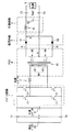
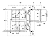
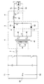
図1は本発明の第1の実施の形態に係るスイッチング電源装置の回路構成を表すものである。図2は図1のスイッチング電源装置のうちトランスの構造を展開して表すものである。このスイッチング電源装置は、高圧バッテリHBから供給される高圧の直流入力電圧Vinを、より低い直流出力電圧Voutに変換して、負荷Lに供給するDC−DCコンバータとして機能するものであり、後述するように2次側がセンタタップ型のスイッチング電源装置である。
[First Embodiment]
FIG. 1 shows a circuit configuration of a switching power supply apparatus according to the first embodiment of the present invention. FIG. 2 shows an expanded structure of the transformer in the switching power supply device of FIG. This switching power supply device functions as a DC-DC converter that converts the high-voltage DC input voltage Vin supplied from the high-voltage battery HB into a lower DC output voltage Vout and supplies the same to the load L, which will be described later. Thus, the secondary side is a center tap type switching power supply device.
このスイッチング電源装置は、一次側高圧ラインL1Hと1次側低圧ラインL1Lとの間に設けられたインバータ回路1(スイッチング回路)および平滑コンデンサ2と、互いに直列に接続された1次側巻線42および1次側巻線43からなる1次側巻線44ならびに互いに直列に接続された2次側巻線45および2次側巻線46からなる2次側巻線47を含んで構成されたトランス4と、インバータ回路1とトランス4との間に設けられた共振用インダクタ3とを備える。1次側高圧ラインL1Hに入力端子T1が、1次側低圧ラインL1Lに入力端子T2がそれぞれ設けられており、これら入力端子T1,T2が高圧バッテリの出力端子と接続されるようになっている。
This switching power supply includes an inverter circuit 1 (switching circuit) and a smoothing
このスイッチング電源装置はまた、トランス4の2次側に設けられた整流回路5と平滑回路6とを備える。平滑回路6の高圧側のラインである出力ラインL0に出力端子T3が、平滑回路6の低圧側のラインである接地ラインLGに出力端子T4がそれぞれ設けられており、これら出力端子T3,T4が負荷の入出力端子と接続されるようになっている。なお、整流回路5および平滑回路6からなる回路が本発明の「整流平滑回路」に対応する。
The switching power supply device also includes a
インバータ回路1は、高圧バッテリから出力される直流入力電圧Vinをほぼ矩形波状の単相交流電圧に変換する単相インバータ回路である。このインバータ回路1は、制御回路(図示せず)から供給されるスイッチング信号によってそれぞれ駆動される4つのスイッチング素子11,12,13,14をフルブリッジ接続してなるフルブリッジ型のスイッチング回路である。スイッチング素子としては、例えば、MOS−FET(Metal Oxide Semiconductor-Field Effect Transistor )やIGBT(Insulated Gate Bipolor Transistor )などの素子が用いられる。
The
スイッチング素子11は、共振用インダクタ3の一端と1次側高圧ラインL1Hとの間に設けられ、スイッチング素子12は共振用インダクタ3の一端と1次側低圧ラインL1Lとの間に設けられている。スイッチング素子13はトランス4の1次側巻線43の一端と1次側高圧ラインL1Hとの間に設けられ、スイッチング素子14は1次側巻線43の一端と1次側低圧ラインL1Lとの間に設けられている。
The switching
これより、インバータ回路1は、スイッチング素子11,14のオン動作により、1次側高圧ラインL1Hから順にスイッチング素子11、共振用インダクタ3、1次側巻線42およびスイッチング素子14を通って1次側低圧ラインL1Lに至る第1の電流経路に電流が流れる一方、スイッチング素子12,13のオン動作により、1次側高圧ラインL1Hから順にスイッチング素子13、1次側巻線42、共振用インダクタ3およびスイッチング素子12を通って1次側低圧ラインL1Lに至る第2の電流経路に電流が流れるようになっている。
As a result, the
共振用インダクタ3は、スイッチング素子11,12,13,14の寄生容量の少なくとも1つと共に共振回路を構成するようになっており、その共振特性を利用して、スイッチング素子のオン・オフによって生じる電力損失を低減するようになっている。なお、共振用インダクタ3は、コイル部品を実際に配置して構成されていてもよいが、これに代えて(これと共に)、トランス4の漏洩インダクタンスや配線などを含めた直列インダクタンスを利用して構成されていてもよい。
The
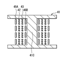
トランス4は、互いに直列に接続された1次側巻線42(1次側第1巻線グループ)および1次側巻線43(1次側第2巻線グループ)からなる1次側巻線44(1次側巻線グループ)と、互いに直列に接続された2次側巻線45(2次側第1巻線グループ)および2次側巻線46(2次側第2巻線グループ)からなる2次側巻線47(2次側巻線グループ)とが互いに同じ向きの極性を有するように磁芯41に巻回されることにより磁気結合された磁気素子である。このトランス4は、降圧型のトランスであり、2次側巻線45および2次側巻線46のそれぞれの巻き数が、1次側巻線44のそれよりも少なくなっている。なお、降圧の度合いは、1次側巻線44の巻き数と、2次側巻線45および2次側巻線46のそれぞれの巻き数との比によって定まる。
The
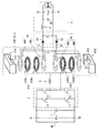
磁芯41は、8の字状の磁路を有し、例えば、それぞれE型形状の磁芯41Aおよび磁芯41Bからなり、磁芯41Aを導電性の支持基体(図示せず)上に載置すると共にその磁芯41A上に磁芯41Bを重ね合わせて構成されたものである。磁芯41A上に磁芯41Bを重ね合わせることにより磁心41の中心部分に円柱状の中足41Cが形成されるようになっている。この中足41Cは、トランス4の1次側巻線44、2次側巻線45および2次側巻線46を巻回するためのものである。
The
2次側巻線45は互いに並列に接続された2次側巻線45A(2次側第1サブ巻線グループ)および2次側巻線45B(2次側第2サブ巻線グループ)を、2次側巻線46は互いに並列に接続された2次側巻線46A(2次側第3サブ巻線グループ)および2次側巻線46B(2次側第4サブ巻線グループ)をそれぞれ有する。これら2次側巻線45A、2次側巻線45B、2次側巻線46Aおよび2次側巻線46Bは、中足41Cの延在方向に垂直な面内で中足41Cにそれぞれ1巻きされたものであり、上からこの順に積層配置されている。
The secondary winding 45 includes a secondary winding 45A (secondary first sub-winding group) and a secondary winding 45B (secondary second sub-winding group) connected in parallel to each other. The secondary winding 46 includes a secondary winding 46A (secondary third sub-winding group) and a secondary winding 46B (secondary fourth sub-winding group) connected in parallel to each other. Have. The secondary side winding 45A, the secondary side winding 45B, the secondary side winding 46A and the secondary side winding 46B are each wound on the
2次側巻線45の一端は後述のダイオード51のアノードに、2次側巻線45の他端はセンタタップCにそれぞれ接続されている。一方、2次側巻線46の一端は後述のダイオード52のアノードに、2次側巻線46の他端はセンタタップCにそれぞれ接続されている。センタタップCは接地ラインLGを介して出力端子T4に接続されている。つまり、トランス4の2次側はセンタタップ型の接続となっている。2次側巻線45および2次側巻線46は、後述のように、整流回路5によって時分割で互いに逆位相に駆動されるようになっている。
One end of the secondary winding 45 is connected to the anode of a
1次側巻線42は、互いに直列に接続された1次側巻線42A(1次側第1サブ巻線グループ)および1次側巻線42B(1次側第2サブ巻線グループ)を有する。これら1次側巻線42Aおよび1次側巻線42Bは、中足41Cの延在方向に垂直な面内で中足41Cにそれぞれ3巻きされたものであり、上からこの順に積層配置されている。さらに、1次側巻線42は、2次側巻線45Aおよび2次側巻線45Bにサンドイッチされており、1次側巻線42Aが2次側巻線45Aに近接配置されると共に1次側巻線42Bが2次側巻線45Bに近接配置されている。これより、1次側巻線42は、2次側巻線46よりも2次側巻線45により近く配置されている。
The primary side winding 42 includes a primary side winding 42A (primary side first sub-winding group) and a primary side winding 42B (primary side second sub-winding group) connected in series to each other. Have. The primary side winding 42A and the primary side winding 42B are wound around the
1次側巻線43は、互いに直列に接続された1次側巻線43A(1次側第3サブ巻線グループ)および1次側巻線43B(1次側第4サブ巻線グループ)を有する。これら1次側巻線43Aおよび1次側巻線43Bは、中足41Cの延在方向に垂直な面内で中足41Cにそれぞれ3巻きされたものであり、上からこの順に積層配置されている。さらに、1次側巻線43は、2次側巻線46Aおよび2次側巻線46Bにサンドイッチされており、1次側巻線43Aが2次側巻線46Aに隣接配置されると共に1次側巻線43Bが2次側巻線46Bに隣接配置されている。これより、1次側巻線43は、2次側巻線45よりも2次側巻線46により近く配置されている。
The primary side winding 43 includes a primary side winding 43A (primary side third sub-winding group) and a primary side winding 43B (primary side fourth sub-winding group) connected in series to each other. Have. The primary side winding 43A and the primary side winding 43B are wound around the
これより、トランス4は、1次側の巻線(1次側巻線42,43)と、2次側の巻線(2次側巻線45,46)とを交互に(サンドイッチ状に)積層する構造を有しており、電流が同一方向に流れる1次側巻線42および1次側巻線43が互いに近接しないようになっている。また、トランス4の各巻線は、2次側巻線45A(2次側第1サブ巻線グループ)、1次側巻線42A(1次側第1サブ巻線グループ)、1次側巻線42B(1次側第2サブ巻線グループ)、2次側巻線45B(2次側第2サブ巻線グループ)、2次側巻線46A(2次側第3サブ巻線グループ)、1次側巻線43A(1次側第3サブ巻線グループ)、1次側巻線43B(1次側第4サブ巻線グループ)および2次側巻線46B(2次側第4サブ巻線グループ)を上からこの順に積層して配置されている。すなわち、トランス4の積層構造が上下対称となっている。
As a result, the
これら1次側巻線42および1次側巻線43は、インバータ回路1の動作に応じて自身に流れる電流の方向が変化するようにインバータ回路1に接続されている。具体的には、1次側巻線42の一端が共振用インダクタ3を介してスイッチング素子11とスイッチング素子12との接続点に接続され、1次側巻線42の他端が1次側巻線43の一端に接続され、1次側巻線43の他端がスイッチング素子13とスイッチング素子14との接続点に接続されている。
The primary side winding 42 and the primary side winding 43 are connected to the
なお、上記した1次側巻線42A、1次側巻線42B、1次側巻線43A、1次側巻線43B、2次側巻線45、2次側巻線45B、2次側巻線46Aおよび2次側巻線46Bは、空気で互いに絶縁されていてもよいし、図示しない絶縁シートを挟むことにより互いに絶縁されていてもよい。
The primary side winding 42A, the primary side winding 42B, the primary side winding 43A, the primary side winding 43B, the secondary side winding 45, the secondary side winding 45B, and the secondary side winding described above. The
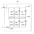
ここで、トランス4の1次側の巻線、すなわち、1次側巻線42および1次側巻線43からなる1次側巻線44は、図3に示したような等価回路で表すことができる。すなわち、この等価回路は、回路a1と、回路a2と、インダクタンスLe1とを互いに直列に接続した回路である。回路a1は、互いに直列に接続されたインダクタンスL1および抵抗R1と、互いに直列に接続されたインダクタンスL2および抵抗R2と、互いに直列に接続された線間容量C1および抵抗R3とを互いに並列に接続して構成されている。回路a2は、互いに直列に接続されたインダクタンスL3および抵抗R4と、互いに直列に接続されたインダクタンスL4および抵抗R5と、互いに直列に接続された線間容量C2および抵抗R6をと互いに並列に接続して構成されている。
Here, the primary side winding of the
上記において、インダクタンスL1はトランス4を理想トランスとしたときの1次側巻線42のインダクタンスであり、抵抗R1はトランス4を理想トランスとしたときの1次側巻線42の抵抗である。インダクタンスL2は1次側巻線42の励磁インダクタンスであり、抵抗R2は1次側巻線42の交流抵抗成分である。線間容量C1は1次側巻線42内の線間容量と、1次側巻線42および2次側巻線45,46の線間容量との合計容量であり、抵抗R3は1次側巻線42の交流抵抗成分である。インダクタンスL3はトランス4を理想トランスとしたときの1次側巻線43のインダクタンスであり、抵抗R4はトランス4を理想トランスとしたときの1次側巻線43の抵抗である。インダクタンスL4は1次側巻線43の励磁インダクタンスであり、抵抗R5は1次側巻線43の交流抵抗成分である。線間容量C2は1次側巻線43内の線間容量と、1次側巻線43および2次側巻線45,46の線間容量との合計容量であり、抵抗R6は1次側巻線43の交流抵抗成分である。インダクタンスLe1はトランス4の漏洩インダクタンスである。
In the above, the inductance L1 is the inductance of the primary side winding 42 when the
整流回路5は、一対のダイオード51(第1整流素子)およびダイオード52(第2整流素子)からなる単相全波整流型のものである。ダイオード51のアノードは2次側巻線45の一端に、ダイオード51のカソードは接続点Dにそれぞれ接続されている。ダイオード52のアノードは2次側巻線46の一端に、ダイオード52のカソードは接続点Dにそれぞれ接続されている。接続点Dは平滑回路6を介して出力端子T3に接続されている。これにより、この整流回路5は、2次側巻線45と2次側巻線46とが時分割で互いに逆位相に駆動されるようになっている。
The
平滑回路6は、チョークコイル61と、平滑コンデンサ62とを含んで構成されており、整流回路5で整流された直流電圧を平滑化して直流出力電圧Voutを生成し、これを出力端子T3,T4から負荷Lに供給するようになっている。
The smoothing
次に、以上のような構成のスイッチング電源装置の作用を説明する。なお、以下では、一般的なスイッチング動作でインバータ回路1を駆動する場合について説明するが、例えば、ゼロボルトスイッチング(Zero Volto Switching)動作でインバータ回路1を駆動することも可能である。
Next, the operation of the switching power supply device configured as described above will be described. In the following, the case where the
インバータ回路1のスイッチング素子11,14がオンすると、スイッチング素子11からスイッチング素子14の方向に電流が流れ、トランス4の1次側巻線44に電圧Vin1が現れると共に、1次側巻線44を構成する1次側巻線42および1次側巻線43に電流Iin1が流れる。一方、トランス4の2次側巻線45,46に、ダイオード52に対して逆方向となり、ダイオード51に対して順方向となる電圧が現れる。このため、2次側巻線45、チョークコイル61および平滑コンデンサ62を通って出力ラインLOおよび接地ラインLGに電流Iout1が流れる。このとき、平滑コンデンサ62に並列に接続された出力端子T3およびT4には平滑回路6によって平滑化された電圧Voutが出力される。
When the switching
次に、スイッチング素子11,14がオンからオフになると、トランス4の2次側巻線45,46に、ダイオード52に対して順方向となる電圧が現れる。このため、2次側巻線45、チョークコイル61および平滑コンデンサ62を通って出力ラインLOおよび接地ラインLGに電流が流れる。このとき、平滑コンデンサ62に並列に接続された出力端子T3およびT4には平滑回路6によって平滑化された電圧Voutが出力される。
Next, when the switching
次に、スイッチング素子12,13がオンすると、スイッチング素子13からスイッチング素子12の方向に電流が流れ、トランス4の1次側巻線44に電圧Vin2が現れると共に、1次側巻線44を構成する1次側巻線42および1次側巻線43に電流Iin2が流れる。一方、トランス4の2次側巻線45,46に、ダイオード52に対して順方向となり、ダイオード51に対して逆方向となる電圧が現れる。このため、2次側巻線45、チョークコイル61および平滑コンデンサ62を通って出力ラインLOおよび接地ラインLGに電流Iout2が流れる。このとき、平滑コンデンサ62に並列に接続された出力端子T3およびT4には平滑回路6によって平滑化された電圧Voutが出力される。
Next, when the switching
最後に、スイッチング素子12,13がオンからオフになると、トランス4の2次側巻線45,46に、ダイオード51に対して順方向となる電圧が現れる。このため、2次側巻線45、チョークコイル61および平滑コンデンサ62を通って出力ラインLOおよび接地ラインLGに電流が流れる。このとき、平滑コンデンサ62に並列に接続された出力端子T3およびT4には平滑回路6によって平滑化された電圧Voutが出力される。
Finally, when the switching
このようにして、スイッチング電源装置は、高圧バッテリから供給された直流入力電圧Vinを直流出力電圧Voutに変圧(降圧)し、その変圧した直流出力電圧Voutを低圧バッテリに給電する。 In this way, the switching power supply device transforms (steps down) the DC input voltage Vin supplied from the high voltage battery to the DC output voltage Vout, and supplies the transformed DC output voltage Vout to the low voltage battery.
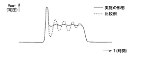
次に、本実施の形態のスイッチング電源装置の効果を比較例と対比して説明する。 Next, the effect of the switching power supply device of the present embodiment will be described in comparison with a comparative example.
比較例では、図4および図5に示したように、トランス104の1次側巻線144は1次側巻線142と1次側巻線143とを互いに並列に接続して構成されており、この点で本実施の形態の1次側巻線44と相違する。
In the comparative example, as shown in FIGS. 4 and 5, the primary side winding 144 of the
比較例の1次側巻線142は、本実施の形態の1次側巻線42と同様、互いに直列に接続された1次側巻線142Aおよび1次側巻線142Bを有する。これら1次側巻線142Aおよび1次側巻線142Bは、中足41Cの延在方向に垂直な面内で中足41Cにそれぞれ6巻きされたものであり、上からこの順に積層配置されている。なお、本実施の形態と比較例との間でトランスの降圧の度合いを揃える観点から、1次側巻線142の巻数を、1次側巻線42の巻数の2倍、すなわち12巻きとしている。さらに、1次側巻線142は、2次側巻線45Aおよび2次側巻線45Bにサンドイッチされており、1次側巻線142Aが2次側巻線45Aに近接配置されると共に1次側巻線142Bが2次側巻線45Bに近接配置されている。これより、1次側巻線142は、2次側巻線46よりも2次側巻線45により近く配置されている。
The primary side winding 142 of the comparative example has a primary side winding 142A and a primary side winding 142B connected in series to each other like the primary side winding 42 of the present embodiment. The primary side winding 142A and the primary side winding 142B are wound around the
比較例の1次側巻線143は、互いに直列に接続された1次側巻線143Aおよび1次側巻線143Bを有する。これら1次側巻線143Aおよび1次側巻線143Bは、中足41Cの延在方向に垂直な面内で中足41Cにそれぞれ6巻きされたものであり、上からこの順に積層配置されている。なお、本実施の形態と比較例との間でトランスの降圧の度合いを揃える観点から、1次側巻線143の巻数を、1次側巻線43の巻数の2倍、すなわち12巻きとしている。さらに、1次側巻線143は、2次側巻線46Aおよび2次側巻線46Bにサンドイッチされており、1次側巻線143Aが2次側巻線46Aに隣接配置されると共に1次側巻線143Bが2次側巻線46Bに隣接配置されている。これより、1次側巻線143は、2次側巻線45よりも2次側巻線46により近く配置されている。
The primary side winding 143 of the comparative example has a primary side winding 143A and a primary side winding 143B connected in series with each other. These primary winding 143A and the primary winding 143B, which has been respectively 6 around the
ここで、比較例のトランス104の1次側の巻線、すなわち、1次側巻線142および1次側巻線143からなる1次側巻線144は、図6に示したような等価回路で表すことができる。すなわち、この等価回路は、回路a101および回路a102を互いに並列に接続してなる回路と、インダクタンスLe101とを互いに直列に接続した回路である。回路a101は、互いに直列に接続されたインダクタンスL101および抵抗R101と、互いに直列に接続されたインダクタンスL102および抵抗R102と、互いに直列に接続された線間容量C101および抵抗R103とを互いに並列に接続して構成されている。回路a102は、互いに直列に接続されたインダクタンスL103および抵抗R104と、互いに直列に接続されたインダクタンスL104および抵抗R105と、互いに直列に接続された線間容量C102および抵抗R106をと互いに並列に接続して構成されている。
Here, the primary side winding 144 of the
上記において、インダクタンスL101はトランス104を理想トランスとしたときの1次側巻線142のインダクタンスであり、抵抗R101はトランス104を理想トランスとしたときの1次側巻線142の抵抗である。インダクタンスL102は1次側巻線142の励磁インダクタンスであり、抵抗R102は1次側巻線142の交流抵抗成分である。線間容量C101は1次側巻線142内の線間容量と、1次側巻線142および2次側巻線45,46の線間容量との合計容量であり、抵抗R103は1次側巻線142の交流抵抗成分である。インダクタンスL103はトランス104を理想トランスとしたときの1次側巻線143のインダクタンスであり、抵抗R104はトランス104を理想トランスとしたときの1次側巻線143の抵抗である。インダクタンスL104は1次側巻線143の励磁インダクタンスであり、抵抗R105は1次側巻線143の交流抵抗成分である。線間容量C102は1次側巻線143内の線間容量と、1次側巻線143および2次側巻線45,46の線間容量との合計容量であり、抵抗R106は1次側巻線143の交流抵抗成分である。インダクタンスLe101はトランス104の漏洩インダクタンスである。
In the above, the inductance L101 is the inductance of the primary side winding 142 when the
比較例では、図7に示したように、1次側巻線144に電圧Vin1が入力されると、1次側巻線142に電流Iin11が、1次側巻線143に電流Iin12がそれぞれ流れる。ここで、1次側巻線142は電流の流れている2次側巻線45により近く配置されているので、2次側巻線45と密に磁気結合する。このとき、1次側巻線142と2次側巻線45とはトランスの原理上、電流の流れる向きが互いに逆向きになるので、1次側巻線142では、電流の流れる向きが同一である巻線グループ同士を近接させた場合と比べて、近接効果による影響が低下するので交流抵抗が低くなる。これより、1次側巻線142には相対的に大きな電流が流れる。一方、1次側巻線143は電流の流れている2次側巻線45により遠く配置されているので、2次側巻線45と疎に磁気結合する。このとき、電流が流れていない2次側巻線46に相対的に近く配置されているので、1次側巻線143では、1次側巻線142と比べて、近接効果により交流抵抗が高くなる。これより、1次側巻線143には相対的に小さな電流しか流れない。 In the comparative example, as shown in FIG. 7, when the voltage Vin1 is input to the primary side winding 144, the current Iin11 flows through the primary side winding 142, and the current Iin12 flows through the primary side winding 143, respectively. . Here, since the primary side winding 142 is disposed closer to the secondary side winding 45 through which a current flows, the primary side winding 142 is closely magnetically coupled to the secondary side winding 45. At this time, the primary side winding 142 and the secondary side winding 45 are opposite in direction of current flow due to the principle of the transformer. Therefore, in the primary side winding 142, the direction of current flow is the same. Compared with the case where certain winding groups are brought close to each other, the influence of the proximity effect is reduced, so that the AC resistance is lowered. As a result, a relatively large current flows through the primary winding 142. On the other hand, since the primary winding 143 is disposed farther than the secondary winding 45 through which current flows, the primary winding 143 is loosely magnetically coupled to the secondary winding 45. At this time, since the secondary winding 46 is arranged relatively close to no current flowing, the primary winding 143 has a higher AC resistance due to the proximity effect than the primary winding 142. Become. As a result, only a relatively small current flows through the primary winding 143.
また、図8に示したように、1次側巻線144に電圧Vin2が入力されると、1次側巻線142に電流Iin22が、1次側巻線143に電流Iin21がそれぞれ流れる。ここで、1次側巻線143は電流の流れている2次側巻線46により近く配置されているので、2次側巻線46と相対的に密に磁気結合する。このとき、1次側巻線143と2次側巻線46とはトランスの原理上、電流の流れる向きが互いに逆向きになるので、1次側巻線143では、電流の流れる向きが同一である巻線グループ同士を近接させた場合と比べて、近接効果による影響が低下するので交流抵抗が低くなる。これより、1次側巻線143には相対的に大きな電流が流れる。一方、1次側巻線142は電流の流れている2次側巻線46により遠く配置されているので、2次側巻線46と相対的に疎に磁気結合する。このとき、電流が流れていない2次側巻線45に相対的に近く配置されているので、1次側巻線142では、1次側巻線143と比べて、近接効果により交流抵抗が高くなる。これより、1次側巻線142には相対的に小さな電流しか流れない。 As shown in FIG. 8, when the voltage Vin <b> 2 is input to the primary side winding 144, the current Iin22 flows through the primary side winding 142 and the current Iin21 flows through the primary side winding 143. Here, since the primary side winding 143 is disposed closer to the secondary side winding 46 through which a current flows, the primary side winding 143 is magnetically coupled relatively closely to the secondary side winding 46. At this time, the primary side winding 143 and the secondary side winding 46 have the same current flowing direction in the primary side winding 143 because the current flows in opposite directions due to the principle of the transformer. Compared with the case where certain winding groups are brought close to each other, the influence of the proximity effect is reduced, so that the AC resistance is lowered. As a result, a relatively large current flows through the primary winding 143. On the other hand, since the primary side winding 142 is disposed farther than the secondary side winding 46 through which current flows, the primary side winding 142 is magnetically coupled to the secondary side winding 46 relatively loosely. At this time, since the secondary winding 45 is arranged relatively close to the current not flowing, the primary winding 142 has a higher AC resistance due to the proximity effect than the primary winding 143. Become. As a result, only a relatively small current flows through the primary winding 142.
このように、比較例では、1次側巻線142および1次側巻線143が互いに並列に接続されているので、交流抵抗の低い側の巻線に電流のより多くが流れることとなる。そのため、トランス104の線間容量C1およびC2と、トランス104の励磁インダクタンスL2およびL4と、トランス104の漏洩インダクタンスLe1とによるLC共振によって生じる、トランス104の出力交流電圧(図4および図5中の端部Aおよび端部B間の電圧)に発生するリンギングを、低い交流抵抗によって減衰させることはほとんどできない(図9の点線で示された波形参照)。その結果、トランス104におけるコアロスやトランス104の交流抵抗による発熱量が増加し、効率が低下してしまう。
Thus, in the comparative example, the primary side winding 142 and the primary side winding 143 are connected in parallel to each other, so that a larger amount of current flows through the winding on the side having a low AC resistance. Therefore, the output AC voltage of the transformer 104 (in FIG. 4 and FIG. 5) generated by LC resonance due to the line capacitances C1 and C2 of the
一方、本実施の形態では、図10に示したように、1次側巻線44に電圧Vin1が入力されると、1次側巻線44を構成する1次側巻線42および1次側巻線43に電流Iin1が流れる。ここで、1次側巻線42は電流の流れている2次側巻線45により近く配置されているので、2次側巻線45と相対的に密に磁気結合する。このとき、1次側巻線42と2次側巻線45とはトランスの原理上、電流の流れる向きが互いに逆向きになるので、1次側巻線42では、電流の流れる向きが同一である巻線グループ同士を近接させた場合と比べて、近接効果による影響が低下するので交流抵抗が低くなる。一方、1次側巻線43は電流の流れている2次側巻線45により遠く配置されているので、2次側巻線45と相対的に疎に磁気結合する。このとき、電流が流れていない2次側巻線46により近く配置されているので、1次側巻線43では、1次側巻線42と比べて、近接効果により交流抵抗が高くなるが、本実施の形態では、1次側巻線42および1次側巻線43は互いに直列に接続されているので、1次側巻線42および1次側巻線43には互いに等しい電.流が流れる。 On the other hand, in the present embodiment, as shown in FIG. 10, when voltage Vin <b> 1 is input to primary side winding 44, primary side winding 42 and primary side constituting primary side winding 44. A current Iin1 flows through the winding 43. Here, since the primary side winding 42 is disposed closer to the secondary side winding 45 through which a current flows, the primary side winding 42 is magnetically coupled to the secondary side winding 45 relatively closely. At this time, since the primary side winding 42 and the secondary side winding 45 are opposite in direction of current flow due to the principle of the transformer, the direction of current flow is the same in the primary side winding 42. Compared with the case where certain winding groups are brought close to each other, the influence of the proximity effect is reduced, so that the AC resistance is lowered. On the other hand, since the primary side winding 43 is disposed farther than the secondary side winding 45 through which a current flows, the primary side winding 43 is magnetically coupled to the secondary side winding 45 relatively loosely. At this time, since the secondary side winding 46 in which no current flows is arranged closer, the primary side winding 43 has higher AC resistance due to the proximity effect than the primary side winding 42. In the present embodiment, since the primary side winding 42 and the primary side winding 43 are connected in series with each other, the primary side winding 42 and the primary side winding 43 have the same voltage. The current flows.
また、図11に示したように、1次側巻線44に電圧Vin2が入力されると、1次側巻線44を構成する1次側巻線42および1次側巻線43に電流Iin2が流れる。ここで、1次側巻線43は電流の流れている2次側巻線46により近く配置されているので、2次側巻線46と相対的に密に磁気結合する。このとき、1次側巻線43と2次側巻線46とはトランスの原理上、電流の流れる向きが互いに逆向きになるので、1次側巻線43では、電流の流れる向きが同一である巻線グループ同士を近接させた場合と比べて、近接効果による影響が低下するので交流抵抗が低くなる。一方、1次側巻線42は電流の流れている2次側巻線46により遠く配置されているので、2次側巻線46と相対的に疎に磁気結合する。このとき、電流が流れていない2次側巻線45により近く配置されているので、1次側巻線42では、1次側巻線43と比べて、近接効果により交流抵抗が高くなるが、本実施の形態では、1次側巻線42および1次側巻線43は互いに直列に接続されているので、1次側巻線42および1次側巻線43には互いに等しい電流が流れる。 As shown in FIG. 11 , when the voltage Vin2 is input to the primary side winding 44, the current Iin2 is supplied to the primary side winding 42 and the primary side winding 43 that constitute the primary side winding 44. Flows. Here, since the primary side winding 43 is disposed closer to the secondary side winding 46 through which a current flows, the primary side winding 43 is magnetically coupled to the secondary side winding 46 relatively closely. At this time, the primary side winding 43 and the secondary side winding 46 are opposite in direction of current flow due to the principle of the transformer. Therefore, in the primary side winding 43, the direction of current flow is the same. Compared with the case where certain winding groups are brought close to each other, the influence of the proximity effect is reduced, so that the AC resistance is lowered. On the other hand, since the primary side winding 42 is disposed farther than the secondary side winding 46 through which a current flows, the primary side winding 42 is magnetically coupled to the secondary side winding 46 relatively loosely. At this time, since the secondary side winding 45 where current does not flow is arranged closer, the primary side winding 42 has higher AC resistance due to the proximity effect than the primary side winding 43, In the present embodiment, since the primary side winding 42 and the primary side winding 43 are connected to each other in series, equal currents flow through the primary side winding 42 and the primary side winding 43.
このように、本実施の形態では、1次側巻線42および1次側巻線43が互いに直列に接続されているので、交流抵抗の大きな巻線にも大きな電流が流れることとなる。そのため、トランス4の線間容量C1およびC2と、トランス4の励磁インダクタンスL2およびL4と、トランス4の漏洩インダクタンスLe1とによるLC共振によって生じる、トランス4の出力交流電圧(図1および図2中の端部Aおよび端部B間の電圧)に発生するリンギングを、高い交流抵抗によって減衰させることができる(図9の実線で示された波形参照)。その結果、トランス4におけるコアロスやトランス4の交流抵抗による発熱量が低下し、効率が向上する。
Thus, in the present embodiment, since the primary side winding 42 and the primary side winding 43 are connected in series with each other, a large current also flows through the winding having a large AC resistance. Therefore, the output AC voltage of the transformer 4 (in FIG. 1 and FIG. 2) generated by LC resonance due to the line capacitances C1 and C2 of the
また、本実施の形態では、トランス4の各巻線(1次側巻線42A、1次側巻線42B、1次側巻線43A、1次側巻線43B、2次側巻線45A、2次側巻線45B、2次側巻線46Aおよび2次側巻線46B)の積層構造が上下対称となっているので、2次側巻線45が駆動されているときと、2次側巻線46が駆動されているときとで、トランス4の交流抵抗の大きさに実質的な差異はない。これより、2次側巻線45が駆動されているときの出力交流電圧と、2次側巻線46が駆動されているときの出力交流電圧とで、リンギングの減衰量に実質的な差異はないので、発熱量が周期的に増大することもなく、高効率を維持することができる。
In the present embodiment, each winding of the transformer 4 (primary winding 42A, primary winding 42B, primary winding 43A, primary winding 43B, secondary winding 45A, 2 Since the laminated structure of the secondary winding 45B, the secondary winding 46A, and the secondary winding 46B) is vertically symmetric, the secondary winding 45 and the secondary winding 45 are driven. There is no substantial difference in the magnitude of the AC resistance of the
[第1の実施の形態の変形例]
上記実施の形態では、トランス4の各巻線は、2次側巻線45A、1次側巻線42A、1次側巻線42B、2次側巻線45B、2次側巻線46A、1次側巻線43A、1次側巻線43Bおよび2次側巻線46Bを上からこの順に積層して配置されていたが、図12に示したように、上下対称を維持した状態で、2次側巻線45Bおよび2次側巻線46Aの間に、1次側第3巻線47Aおよび1次側第3巻線47Bを上からこの順に積層してなる1次側第3巻線47を挿入配置してもよい。また、上下対称を維持した状態で、図13に示したように、2次側巻線45Bおよび2次側巻線46Aを削除したり、図14に示したように、2次側巻線45Aおよび2次側巻線46Bを削除してもよい。なお、上下対称ではないが、図15に示したように、2次側巻線45Bおよび2次側巻線46Bを削除してもよい。いずれにおいても、大きな交流抵抗が1次側巻線44中に直列に配置されるようになっていればよい。
[Modification of First Embodiment]
In the above embodiment, each winding of the
また、上記実施の形態では、トランス4の各巻線は、中足41Cの延在方向に垂直な面内で中足41Cに巻回されていたが、図16ないし図19に示したように、中足41Cの延在方向に平行な円筒面内で中足41Cに巻回されていてもよい。
In the above embodiment, each winding of the
[第2の実施の形態]
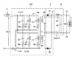
図20は本発明の第2の実施の形態に係るスイッチング電源装置の回路構成を表すものである。図21は図20のスイッチング電源装置のうちトランスの構造を展開して表すものである。このスイッチング電源装置は、上記第1の実施の形態と比較して、インバータ回路10の構成と、インバータ回路10およびトランス40の接続関係と、トランス40の構成とにおいて相違する。そこで、以下、上記第1の実施の形態との相違点について主に説明し、上記第1の実施の形態と共通する構成、作用、効果についての記載を適宜省略する。
[Second Embodiment]
FIG. 20 shows a circuit configuration of a switching power supply apparatus according to the second embodiment of the present invention. FIG. 21 shows an expanded structure of the transformer in the switching power supply device of FIG. This switching power supply apparatus is different from the first embodiment in the configuration of the
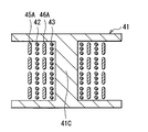
インバータ回路10は、制御回路(図示せず)から供給されるスイッチング信号によってそれぞれ駆動される2つのスイッチング素子15,16を並列接続してなるプッシュプル型のスイッチング回路である。
The
トランス40は、上記実施の形態のトランス4と異なる順番で各巻線を積層して構成したものである。具体的には、上記実施の形態のトランス4の積層構造において、2次側巻線45Bと2次側巻線46Aとが入れ換えられたものであり、2次側巻線45A(2次側第1サブ巻線グループ)、1次側巻線42A(1次側第1サブ巻線グループ)、1次側巻線42B(1次側第2サブ巻線グループ)、2次側巻線46A(2次側第3サブ巻線グループ)、2次側巻線45B(2次側第2サブ巻線グループ)、1次側巻線43A(1次側第4サブ巻線グループ)、1次側巻線43B(1次側第3サブ巻線グループ)および2次側巻線46B(2次側第4サブ巻線グループ)を上からこの順に積層して配置されている。すなわち、トランス40の積層構造は上下対称となっている。
The
スイッチング素子15はトランス40の1次側巻線42Aの一端と1次側低圧ラインL1Lとの間に設けられている。スイッチング素子16は1次側巻線43の一端と1次側高圧ラインL1Hとの間に設けられ、スイッチング素子14は1次側巻線43Bの一端と1次側低圧ラインL1Lとの間に設けられている。共振用インダクタ3は1次側巻線42Bおよび1次側巻線43Aの接続点と1次側高圧ラインL1Hとの間に設けられている。
The switching
ここで、トランス40の1次側の巻線、すなわち、1次側巻線42および1次側巻線43からなる1次側巻線44は、図22に示したような等価回路で表すことができる。まず、1次側巻線42の等価回路は、回路a11と、回路a12と、インダクタンスLe11とを互いに直列に接続した回路である。回路a11は、互いに直列に接続されたインダクタンスL11および抵抗R11と、互いに直列に接続されたインダクタンスL12および抵抗R12と、互いに直列に接続された線間容量C11および抵抗R13とを互いに並列に接続して構成されている。回路a12は、互いに直列に接続されたインダクタンスL13および抵抗R14と、互いに直列に接続されたインダクタンスL14および抵抗R15と、互いに直列に接続された線間容量C12および抵抗R16をと互いに並列に接続して構成されている。一方、1次側巻線43の等価回路は、回路a13と、回路a14と、インダクタンスLe21とを互いに直列に接続した回路である。回路a13は、互いに直列に接続されたインダクタンスL21および抵抗R21と、互いに直列に接続されたインダクタンスL22および抵抗R22と、互いに直列に接続された線間容量C21および抵抗R23とを互いに並列に接続して構成されている。回路a14は、互いに直列に接続されたインダクタンスL23および抵抗R24と、互いに直列に接続されたインダクタンスL24および抵抗R25と、互いに直列に接続された線間容量C22および抵抗R26をと互いに並列に接続して構成されている。
Here, the primary side winding of the
1次側巻線42の等価回路において、インダクタンスL11はトランス40を理想トランスとしたときの1次側巻線42Aのインダクタンスであり、抵抗R11はトランス40を理想トランスとしたときの1次側巻線42Aの抵抗である。インダクタンスL12は1次側巻線42Aの励磁インダクタンスであり、抵抗R12は1次側巻線42Aの交流抵抗成分である。線間容量C11は1次側巻線42A内の線間容量と、1次側巻線42Aおよび2次側巻線45,46の線間容量との合計容量であり、抵抗R13は1次側巻線42Aの交流抵抗成分である。インダクタンスL13はトランス40を理想トランスとしたときの1次側巻線42Bのインダクタンスであり、抵抗R14はトランス40を理想トランスとしたときの1次側巻線42Bの抵抗である。インダクタンスL14は1次側巻線42Bの励磁インダクタンスであり、抵抗R15は1次側巻線42Bの交流抵抗成分である。線間容量C12は1次側巻線42B内の線間容量と、1次側巻線42Bおよび2次側巻線45,46の線間容量との合計容量であり、抵抗R16は1次側巻線42Bの交流抵抗成分である。インダクタンスLe11は1次側巻線42と2次側巻線45,46とで構成されるトランスの漏洩インダクタンスである。
In the equivalent circuit of the primary winding 42, the inductance L11 is the inductance of the primary winding 42A when the
1次側巻線43の等価回路において、インダクタンスL21はトランス40を理想トランスとしたときの1次側巻線43Aのインダクタンスであり、抵抗R21はトランス40を理想トランスとしたときの1次側巻線43Aの抵抗である。インダクタンスL22は1次側巻線43Aの励磁インダクタンスであり、抵抗R22は1次側巻線43Aの交流抵抗成分である。線間容量C21は1次側巻線43A内の線間容量と、1次側巻線43Aおよび2次側巻線45,46の線間容量との合計容量であり、抵抗R23は1次側巻線43Aの交流抵抗成分である。インダクタンスL23はトランス40を理想トランスとしたときの1次側巻線43Bのインダクタンスであり、抵抗R24はトランス40を理想トランスとしたときの1次側巻線43Bの抵抗である。インダクタンスL24は1次側巻線43Bの励磁インダクタンスであり、抵抗R25は1次側巻線43Bの交流抵抗成分である。線間容量C22は1次側巻線43B内の線間容量と、1次側巻線43Bおよび2次側巻線45,46の線間容量との合計容量であり、抵抗R26は1次側巻線43Bの交流抵抗成分である。インダクタンスLe21は1次側巻線43と2次側巻線45,46とで構成されるトランスの漏洩インダクタンスである。
In the equivalent circuit of the primary side winding 43, the inductance L21 is the inductance of the primary side winding 43A when the
次に、以上のような構成のスイッチング電源装置の作用を説明する。インバータ回路1のスイッチング素子15がオンすると、共振用インダクタ3から1次側巻線42B、1次側巻線42A、スイッチング素子15の方向に電流Iin1が流れ、1次側巻線42に電圧Vin1が現れると共に、1次側巻線42を構成する1次側巻線42Aおよび1次側巻線42Bに電流Iin1が流れる。一方、トランス40の2次側巻線45,46に、ダイオード52に対して逆方向となり、ダイオード51に対して順方向となる電圧が現れる。このため、2次側巻線45、チョークコイル61および平滑コンデンサ62を通って出力ラインLOおよび接地ラインLGに電流Iout1が流れる。このとき、平滑コンデンサ62に並列に接続された出力端子T3およびT4には平滑回路6によって平滑化された電圧Voutが出力される。
Next, the operation of the switching power supply device configured as described above will be described. When the switching
次に、スイッチング素子15がオンからオフになると、トランス40の2次側巻線45,46に、ダイオード52に対して順方向となる電圧が現れる。このため、2次側巻線45、チョークコイル61および平滑コンデンサ62を通って出力ラインLOおよび接地ラインLGに電流が流れる。このとき、平滑コンデンサ62に並列に接続された出力端子T3およびT4には平滑回路6によって平滑化された電圧Voutが出力される。
Next, when the switching
次に、スイッチング素子16がオンすると、共振用インダクタ3から1次側巻線43A、1次側巻線43B、スイッチング素子16の方向に電流が流れ、1次側巻線43に電圧Vin2が現れると共に、1次側巻線43を構成する1次側巻線43Aおよび1次側巻線43Bに電流Iin2が流れる。一方、トランス40の2次側巻線45,46に、ダイオード52に対して順方向となり、ダイオード51に対して逆方向となる電圧が現れる。このため、2次側巻線45、チョークコイル61および平滑コンデンサ62を通って出力ラインLOおよび接地ラインLGに電流Iout2が流れる。このとき、平滑コンデンサ62に並列に接続された出力端子T3およびT4には平滑回路6によって平滑化された電圧Voutが出力される。
Next, when the switching
最後に、スイッチング素子16がオンからオフになると、トランス40の2次側巻線45,46に、ダイオード51に対して順方向となる電圧が現れる。このため、2次側巻線45、チョークコイル61および平滑コンデンサ62を通って出力ラインLOおよび接地ラインLGに電流が流れる。このとき、平滑コンデンサ62に並列に接続された出力端子T3およびT4には平滑回路6によって平滑化された電圧Voutが出力される。
Finally, when the switching
このようにして、スイッチング電源装置は、高圧バッテリから供給された直流入力電圧Vinを直流出力電圧Voutに変圧(降圧)し、その変圧した直流出力電圧Voutを低圧バッテリに給電する。 In this way, the switching power supply device transforms (steps down) the DC input voltage Vin supplied from the high voltage battery to the DC output voltage Vout, and supplies the transformed DC output voltage Vout to the low voltage battery.
次に、本実施の形態のスイッチング電源装置の効果を説明する。 Next, the effect of the switching power supply device of this embodiment will be described.
本実施の形態では、図23に示したように、1次側巻線42に電圧Vin1が入力されると、1次側巻線42を構成する1次側巻線42Aおよび1次側巻線42Bに電流Iin1が流れる。ここで、1次側巻線42Aは電流の流れている2次側巻線45により近く配置されているので、2次側巻線45と相対的に密に磁気結合する。このとき、1次側巻線42Aと2次側巻線45とはトランスの原理上、電流の流れる向きが互いに逆向きになるので、1次側巻線42Aでは、電流の流れる向きが同一である巻線グループ同士を近接させた場合と比べて、近接効果による影響が低下するので交流抵抗が低くなる。一方、1次側巻線42Bは電流の流れている2次側巻線45により遠く配置されているので、2次側巻線45と相対的に疎に磁気結合する。このとき、電流が流れていない2次側巻線46により近く配置されているので、1次側巻線42Bでは、1次側巻線42Aと比べて、近接効果により交流抵抗が高くなるが、本実施の形態では、1次側巻線42Aおよび1次側巻線42Bは互いに直列に接続されているので、1次側巻線42Aおよび1次側巻線42Bには互いに等しい電流が流れる。 In the present embodiment, as shown in FIG. 23, when the voltage Vin1 is input to the primary winding 42, the primary winding 42A and the primary winding constituting the primary winding 42 are provided. The current Iin1 flows through 42B. Here, since the primary side winding 42A is disposed closer to the secondary side winding 45 through which a current flows, the primary side winding 42A is magnetically coupled to the secondary side winding 45 relatively closely. At this time, the primary winding 42A and the secondary winding 45 have the same direction of current flow in the primary winding 42A because the current flows in opposite directions due to the principle of the transformer. Compared with the case where certain winding groups are brought close to each other, the influence of the proximity effect is reduced, so that the AC resistance is lowered. On the other hand, the primary side winding 42B is disposed farther away from the secondary side winding 45 through which current flows, so that it is magnetically coupled to the secondary side winding 45 relatively loosely. At this time, since the secondary winding 46 where current does not flow is arranged closer, the primary winding 42B has higher AC resistance due to the proximity effect than the primary winding 42A. In the present embodiment, since the primary side winding 42A and the primary side winding 42B are connected in series with each other, equal currents flow in the primary side winding 42A and the primary side winding 42B.
また、図24に示したように、1次側巻線43に電圧Vin2が入力されると、1次側巻線43を構成する1次側巻線43Aおよび1次側巻線43Bに電流Iin2が流れる。ここで、1次側巻線43Bは電流の流れている2次側巻線46により近く配置されているので、2次側巻線46と相対的に密に磁気結合する。このとき、1次側巻線43Bと2次側巻線46とはトランスの原理上、電流の流れる向きが互いに逆向きになるので、1次側巻線43Bでは、電流の流れる向きが同一である巻線グループ同士を近接させた場合と比べて、近接効果による影響が低下するので交流抵抗が低くなる。一方、1次側巻線43Aは電流の流れている2次側巻線46により遠く配置されているので、2次側巻線46と相対的に疎に磁気結合する。このとき、電流が流れていない2次側巻線45により近く配置されているので、1次側巻線43Aでは、1次側巻線43Bと比べて、近接効果により交流抵抗が高くなるが、本実施の形態では、1次側巻線43Aおよび1次側巻線43Bは互いに直列に接続されているので、1次側巻線43Aおよび1次側巻線43Bには互いに等しい電流が流れる。 As shown in FIG. 24, when the voltage Vin2 is input to the primary side winding 43, the current Iin2 is supplied to the primary side winding 43A and the primary side winding 43B constituting the primary side winding 43. Flows. Here, since the primary side winding 43B is disposed closer to the secondary side winding 46 through which a current flows, the primary side winding 43B is magnetically coupled to the secondary side winding 46 relatively closely. At this time, the primary side winding 43B and the secondary side winding 46 have the same direction of current flow in the primary side winding 43B because the direction of current flow is opposite to each other due to the principle of the transformer. Compared with the case where certain winding groups are brought close to each other, the influence of the proximity effect is reduced, so that the AC resistance is lowered. On the other hand, the primary side winding 43A is disposed farther away from the secondary side winding 46 through which current flows, so that it is magnetically coupled to the secondary side winding 46 relatively loosely. At this time, since the secondary winding 45 where current does not flow is arranged closer, the primary winding 43A has higher AC resistance due to the proximity effect than the primary winding 43B. In the present embodiment, since the primary winding 43A and the primary winding 43B are connected in series with each other, equal currents flow through the primary winding 43A and the primary winding 43B.
このように、本実施の形態では、1次側巻線42Aおよび1次側巻線42B、ならびに1次側巻線43Aおよび1次側巻線43Bがそれぞれ、互いに直列に接続されているので、交流抵抗の大きな巻線にも大きな電流が流れることとなる。そのため、線間容量C21と、励磁インダクタンスL22と、漏洩インダクタンスLe11とによるLC共振や、線間容量C22と、励磁インダクタンスL24と、漏洩インダクタンスLe21とによるLC共振によって生じる、トランス40の出力交流電圧(図20および図21中の端部Aおよび端部B間の電圧)に発生するリンギングを、上記第1の実施の形態と同様に、高い交流抵抗によって減衰させることができる。その結果、トランス40におけるコアロスやトランス40の交流抵抗による発熱量が低下し、効率が向上する。
Thus, in the present embodiment, the primary side winding 42A and the primary side winding 42B, and the primary side winding 43A and the primary side winding 43B are connected in series with each other. A large current also flows through a winding having a large AC resistance. Therefore, the output AC voltage of the
また、本実施の形態では、トランス40の各巻線(1次側巻線42A、1次側巻線42B、1次側巻線43A、1次側巻線43B、2次側巻線45A、2次側巻線45B、2次側巻線46Aおよび2次側巻線46B)の積層構造が上下対称となっているので、2次側巻線45が駆動されているときと、2次側巻線46が駆動されているときとで、トランス4の交流抵抗の大きさに実質的な差異はない。これより、2次側巻線45が駆動されているときの出力交流電圧と、2次側巻線46が駆動されているときの出力交流電圧とで、リンギングの減衰量に実質的な差異はないので、発熱量が周期的に増大することもなく、高効率を維持することができる。
In the present embodiment, each winding of the transformer 40 (primary winding 42A, primary winding 42B, primary winding 43A, primary winding 43B, secondary winding 45A, 2 Since the laminated structure of the secondary winding 45B, the secondary winding 46A, and the secondary winding 46B) is vertically symmetric, the secondary winding 45 and the secondary winding 45 are driven. There is no substantial difference in the magnitude of the AC resistance of the
[第2の実施の形態の変形例]
上記実施の形態では、トランス40の各巻線は、2次側巻線45A、1次側巻線42A、1次側巻線42B、2次側巻線46A、2次側巻線45B、1次側巻線43A、1次側巻線43Bおよび2次側巻線46Bを上からこの順に積層して配置されていたが、図25に示したように、上下対称を維持した状態で、2次側巻線45Bおよび2次側巻線46Aを削除してもよい。なお、図26に示したように、上下対称ではないが、2次側巻線45Bおよび2次側巻線46Bを削除してもよい。なお、この図26では、1次側巻線43Aが1次側第3サブ巻線グループに対応し、1次側巻線43Bが1次側第4サブ巻線グループに対応する。いずれにおいても、大きな交流抵抗が1次側巻線44中に直列に配置されるようになっていればよい。
[Modification of Second Embodiment]
In the above embodiment, each winding of the
また、上記実施の形態では、トランス40の各巻線は、中足41Cの延在方向に垂直な面内で中足41Cに巻回されていたが、図16、図18、図19に示したように、中足41Cの延在方向に平行な円筒面内で中足41Cに巻回されていてもよい。
Further, in the above embodiment, each winding of the
以上、実施の形態を挙げて本発明を説明したが、本発明は、これらに限定されず、種々の変形が可能である。 Although the present invention has been described with reference to the embodiment, the present invention is not limited to these, and various modifications are possible.
例えば、上記実施の形態では、トランス4,40の2次側の等価回路がカソードコモン接続となるように構成していたが、アノードコモン接続となるように構成してもよい。
For example, in the above-described embodiment, the equivalent circuit on the secondary side of the
また、上記実施の形態では、インバータ回路1,10はフルブリッジ型またはプッシュプル型であったが、図27に例示したようなフォーワード型や、図28に例示したようなハーフブリッジ型などであってもよい。
In the above embodiment, the
1,10…インバータ回路、2,62…平滑コンデンサ、3…共振用インダクタ、4,40,104…トランス、5…整流回路、6…平滑回路、11,12,13,14…スイッチング素子、41…磁心、42,42A,42B,43,43A,43B,44,47,47A,47B…1次側巻線、45,45A,45B,46,46A,46B…2次側巻線、51,52…ダイオード、61…チョークコイル、A,B…端部、C…センタタップ、D…接続点、L1H…1次側高圧ライン、L1L…1次側低圧ライン、LO…出力ライン、LG…接地ライン、T1,T2…入力端子、T3,T4…出力端子、Vin…入力直流電圧、Vout…出力直流電圧。
DESCRIPTION OF
Claims (20)
前記1次側巻線グループの電流方向を時分割的に変化させるようにスイッチング動作を行うスイッチング回路と、
前記スイッチング回路の動作に応じて前記2次側巻線グループに現れる交流電圧を整流し平滑化する整流平滑回路と
を備え、
前記2次側第1巻線グループおよび前記2次側第2巻線グループは、前記スイッチング回路の動作に応じて互いに逆位相に時分割駆動され、
前記1次側第1巻線グループと前記2次側巻線グループとの磁気結合は、前記2次側第1巻線グループが駆動されているときにより密となる一方、前記2次側第2巻線グループが駆動されているときにより疎となり、
前記1次側第2巻線グループと前記2次側巻線グループとの磁気結合は、前記2次側第1巻線グループが駆動されているときにより疎となる一方、前記2次側第2巻線グループが駆動されているときにより密となる
ように構成されていることを特徴とするスイッチング電源装置。 A primary side winding group configured by connecting a primary side first winding group and a primary side second winding group in series with each other, a secondary side first winding group, and a secondary side second winding A transformer having a secondary winding group configured by connecting line groups to each other;
A switching circuit that performs a switching operation so as to change the current direction of the primary winding group in a time-sharing manner;
A rectifying / smoothing circuit for rectifying and smoothing an alternating voltage appearing in the secondary winding group according to the operation of the switching circuit;
The secondary side first winding group and the secondary side second winding group are time-division driven in mutually opposite phases according to the operation of the switching circuit,
The magnetic coupling between the primary side first winding group and the secondary side winding group becomes denser when the secondary side first winding group is driven, while the secondary side second winding group becomes denser. It becomes sparser when the winding group is driven,
The magnetic coupling between the primary side second winding group and the secondary side winding group becomes sparser when the secondary side first winding group is driven, while the secondary side second winding group A switching power supply characterized by being configured to be denser when the winding group is driven.
前記1次側巻線グループの電流方向を時分割的に変化させるようにスイッチング動作を行うスイッチング回路と、
前記スイッチング回路の動作に応じて前記2次側第1巻線グループおよび2次側第2巻線グループが互いに逆位相に時分割駆動されるように前記2次側巻線グループに接続された第1整流素子および第2整流素子を有し、前記スイッチング回路の動作に応じて前記2次側巻線グループに現れる交流電圧を整流し平滑化する整流平滑回路と、
を備え、
前記1次側第1巻線グループは、前記2次側第2巻線グループよりも前記2次側第1巻線グループに近く配置され、
前記1次側第2巻線グループは、前記2次側第1巻線グループよりも前記2次側第2巻線グループに近く配置されている
ことを特徴とするスイッチング電源装置。 A primary side winding group configured by connecting a primary side first winding group and a primary side second winding group in series with each other, a secondary side first winding group, and a secondary side second winding A transformer having a secondary winding group configured by connecting line groups to each other;
A switching circuit that performs a switching operation so as to change the current direction of the primary winding group in a time-sharing manner;
The secondary side first winding group and the secondary side second winding group are connected to the secondary side winding group so that the secondary side first winding group and the secondary side second winding group are time-divisionally driven in mutually opposite phases according to the operation of the switching circuit. A rectifying / smoothing circuit having one rectifying element and a second rectifying element, and rectifying and smoothing an alternating voltage appearing in the secondary winding group according to the operation of the switching circuit;
With
The primary side first winding group is disposed closer to the secondary side first winding group than the secondary side second winding group,
The primary side second winding group is disposed closer to the secondary side second winding group than the secondary side first winding group.
前記2次側第1巻線グループ、2次側第2巻線グループ、1次側第1巻線グループおよび1次側第2巻線グループはそれぞれ、前記中足の延在方向に垂直な面内に巻回されている
ことを特徴とする請求項2記載のスイッチング電源装置。 The transformer has a magnetic core provided with a middle leg,
The secondary side first winding group, the secondary side second winding group, the primary side first winding group, and the primary side second winding group are surfaces perpendicular to the extending direction of the middle foot, respectively. The switching power supply device according to claim 2, wherein the switching power supply device is wound inside.
ことを特徴とする請求項3記載のスイッチング電源装置。 The secondary side first winding group, the primary side first winding group, the primary side second winding group, and the secondary side second winding group are laminated in this order. 3. The switching power supply device according to 3.
ことを特徴とする請求項3記載のスイッチング電源装置。 The secondary side first winding group, the primary side first winding group, the secondary side second winding group, and the primary side second winding group are laminated in this order. 3. The switching power supply device according to 3.
前記2次側第1サブ巻線グループ、1次側第1巻線グループ、2次側第2サブ巻線グループ、2次側第3サブ巻線グループ、1次側第2巻線グループおよび2次側第4サブ巻線グループはこの順に積層されている
ことを特徴とする請求項3記載のスイッチング電源装置。 The secondary side first winding group is formed by connecting a secondary side first subwinding group and a secondary side second subwinding group in parallel to each other, and the secondary side second winding group is a secondary side. constituted by connecting a side third sub-winding group and the secondary-side fourth sub-winding group in parallel to each other physician,
The secondary side first sub-winding group, the primary side first winding group, the secondary side second sub winding group, the secondary side third sub winding group, the primary side second winding group and 2 The switching power supply according to claim 3, wherein the secondary fourth sub-winding groups are stacked in this order.
前記2次側第1巻線グループ、2次側第2巻線グループ、1次側第1巻線グループおよび1次側第2巻線グループはそれぞれ、前記中足の延在方向に平行な円筒面内に巻回されている
ことを特徴とする請求項2記載のスイッチング電源装置。 The transformer has a magnetic core provided with a middle leg,
Each of the secondary side first winding group, the secondary side second winding group, the primary side first winding group, and the primary side second winding group is a cylinder parallel to the extending direction of the middle leg. The switching power supply device according to claim 2, wherein the switching power supply device is wound in a plane.
ことを特徴とする請求項7記載のスイッチング電源装置。 The secondary side first winding group, the primary side first winding group, the primary side second winding group, and the secondary side second winding group are laminated in this order. 8. The switching power supply device according to 7.
ことを特徴とする請求項7記載のスイッチング電源装置。 The secondary side first winding group, the primary side first winding group, the secondary side second winding group, and the primary side second winding group are laminated in this order. 8. The switching power supply device according to 7.
前記2次側第1サブ巻線グループ、1次側第1巻線グループ、2次側第2サブ巻線グループ、2次側第3サブ巻線グループ、1次側第2巻線グループおよび2次側第4サブ巻線グループはこの順に積層されている
ことを特徴とする請求項7記載のスイッチング電源装置。 The secondary side first winding group is formed by connecting a secondary side first subwinding group and a secondary side second subwinding group in parallel to each other, and the secondary side second winding group is a secondary side. constituted by connecting a side third sub-winding group and the secondary-side fourth sub-winding group in parallel to each other physician,
The secondary side first sub-winding group, the primary side first winding group, the secondary side second sub winding group, the secondary side third sub winding group, the primary side second winding group and 2 The switching power supply according to claim 7, wherein the secondary fourth sub-winding groups are stacked in this order.
前記1次側第1巻線グループおよび前記1次側第2巻線グループが互いに逆位相に時分割駆動されるようにスイッチング動作を行うスイッチング回路と、
前記スイッチング回路の動作に応じて前記2次側巻線グループに現れる交流電圧を整流し平滑化する整流平滑回路と
を備え、
前記2次側第1巻線グループおよび前記2次側第2巻線グループは、前記スイッチング回路の動作に応じて互いに逆位相に時分割駆動され、
前記1次側第1巻線グループは、前記2次側第1巻線グループが駆動されているときに前記2次側巻線グループとの磁気結合がより密となる1次側第1サブ巻線グループと、より疎となる1次側第2サブ巻線グループとを互いに直列に接続して構成され、
前記1次側第2巻線グループは、前記2次側第2巻線グループが駆動されているときに前記2次側巻線グループとの磁気結合がより密となる1次側第3サブ巻線グループと、より疎となる1次側第4サブ巻線グループとを互いに直列に接続して構成されている
ことを特徴とするスイッチング電源装置。 Primary side winding group configured by connecting primary side first winding group and primary side second winding group to each other, secondary side first winding group and secondary side second winding group A transformer having a secondary winding group configured by connecting together,
A switching circuit that performs a switching operation so that the primary side first winding group and the primary side second winding group are driven in a time-sharing manner in mutually opposite phases;
A rectifying / smoothing circuit for rectifying and smoothing an alternating voltage appearing in the secondary winding group according to the operation of the switching circuit;
The secondary side first winding group and the secondary side second winding group are time-division driven in mutually opposite phases according to the operation of the switching circuit,
The primary side first winding group has a primary side first sub-winding whose magnetic coupling with the secondary side winding group becomes denser when the secondary side first winding group is driven. A line group and a more sparse primary side second subwinding group are connected in series with each other,
The primary side second winding group includes a primary side third sub-winding whose magnetic coupling with the secondary side winding group becomes dense when the secondary side second winding group is driven. A switching power supply device comprising: a line group and a sparser primary fourth sub-winding group connected in series to each other.
前記1次側第1巻線グループおよび前記1次側第2巻線グループが互いに逆位相に時分割駆動されるようにスイッチング動作を行うスイッチング回路と、
前記スイッチング回路の動作に応じて前記2次側第1巻線グループおよび2次側第2巻線グループが互いに逆位相に時分割駆動されるように前記2次側巻線グループに接続された第1整流素子および第2整流素子を有し、前記スイッチング回路の動作に応じて前記2次側巻線グループに現れる交流電圧を整流し平滑化する整流平滑回路と、
を備え、
前記1次側第1巻線グループは、前記2次側第2巻線グループよりも前記2次側第1巻線グループに近く配置された1次側第1サブ巻線グループと、前記2次側第1巻線グループよりも前記2次側第2巻線グループに近く配置された1次側第2サブ巻線グループとを互いに直列に接続して構成され、
前記1次側第2巻線グループは、前記2次側第1巻線グループよりも前記2次側第2巻線グループに近く配置された1次側第3サブ巻線グループと、前記2次側第2巻線グループよりも前記2次側第1巻線グループに近く配置された1次側第4サブ巻線グループとを互いに直列に接続して構成されている
ことを特徴とするスイッチング電源装置。 A primary-winding group to the primary first winding group and the second primary-winding group is constructed by connecting to each other, the first winding secondary-side group and the secondary side, Volume 2 A transformer having a secondary winding group configured by connecting line groups to each other;
A switching circuit that performs a switching operation so that the primary side first winding group and the primary side second winding group are driven in a time-sharing manner in mutually opposite phases;
The secondary side first winding group and the secondary side second winding group are connected to the secondary side winding group so that the secondary side first winding group and the secondary side second winding group are time-divisionally driven in mutually opposite phases according to the operation of the switching circuit. A rectifying / smoothing circuit having one rectifying element and a second rectifying element, and rectifying and smoothing an alternating voltage appearing in the secondary winding group according to the operation of the switching circuit;
With
The primary side first winding group includes a primary side first sub-winding group disposed closer to the secondary side first winding group than the secondary side second winding group, and the secondary side A primary side second sub-winding group arranged closer to the secondary side second winding group than the side first winding group is connected in series with each other;
The primary side second winding group includes a primary side third sub-winding group disposed closer to the secondary side second winding group than the secondary side first winding group, and the secondary side A switching power supply comprising: a primary side fourth sub-winding group arranged closer to the secondary side first winding group than the side second winding group and connected in series to each other apparatus.
前記2次側第1巻線グループ、2次側第2巻線グループ、1次側第1サブ巻線グループ、1次側第2サブ巻線グループ、1次側第3サブ巻線グループおよび1次側第4サブ巻線グループはそれぞれ、前記中足の延在方向に垂直な面内に巻回されている
ことを特徴とする請求項12記載のスイッチング電源装置。 The transformer has a magnetic core provided with a middle leg,
The secondary side first winding group, the secondary side second winding group, the primary side first sub winding group, the primary side second sub winding group, the primary side third sub winding group and 1 The switching power supply according to claim 12, wherein each of the secondary fourth sub-winding groups is wound in a plane perpendicular to the extending direction of the middle leg.
ことを特徴とする請求項13記載のスイッチング電源装置。 The secondary side first winding group, the primary side first sub winding group, the primary side second sub winding group, the secondary side second winding group, the primary side third sub winding group and 1 The switching power supply according to claim 13, wherein the secondary fourth sub-winding groups are stacked in this order.
ことを特徴とする請求項13記載のスイッチング電源装置。 The secondary side first winding group, the primary side first sub winding group, the primary side second sub winding group, the primary side fourth sub winding group, the primary side third sub winding group, and The switching power supply according to claim 13, wherein the secondary side second winding groups are stacked in this order.
前記2次側第1サブ巻線グループ、1次側第1サブ巻線グループ、1次側第2サブ巻線グループ、2次側第3サブ巻線グループ、2次側第2サブ巻線グループ、1次側第4サブ巻線グループ、1次側第3サブ巻線グループおよび2次側第4サブ巻線グループはこの順に積層されている
ことを特徴とする請求項13記載のスイッチング電源装置。 The secondary side first winding group is formed by connecting a secondary side first subwinding group and a secondary side second subwinding group in parallel to each other, and the secondary side second winding group is a secondary side. constituted by connecting a side third sub-winding group and the secondary-side fourth sub-winding group in parallel to each other physician,
Secondary side first sub-winding group, primary side first sub-winding group, primary side second sub-winding group, secondary side third sub-winding group, secondary side second sub-winding group The switching power supply according to claim 13, wherein the primary side fourth sub-winding group, the primary side third sub-winding group, and the secondary side fourth sub-winding group are laminated in this order. .
前記2次側第1巻線グループ、2次側第2巻線グループ、1次側第1サブ巻線グループ、1次側第2サブ巻線グループ、1次側第3サブ巻線グループおよび1次側第4サブ巻線グループはそれぞれ、前記中足の延在方向に平行な円筒面内に巻回されている
ことを特徴とする請求項12記載のスイッチング電源装置。 The transformer has a magnetic core provided with a middle leg,
The secondary side first winding group, the secondary side second winding group, the primary side first sub winding group, the primary side second sub winding group, the primary side third sub winding group and 1 The switching power supply according to claim 12, wherein each of the secondary fourth sub-winding groups is wound in a cylindrical surface parallel to the extending direction of the middle leg.
ことを特徴とする請求項17記載のスイッチング電源装置。 The secondary side first winding group, the primary side first sub winding group, the primary side second sub winding group, the secondary side second winding group, the primary side third sub winding group and 1 The switching power supply according to claim 17, wherein the secondary fourth sub-winding groups are stacked in this order.
ことを特徴とする請求項17記載のスイッチング電源装置。 The secondary side first winding group, the primary side first sub winding group, the primary side second sub winding group, the primary side fourth sub winding group, the primary side third sub winding group, and The switching power supply according to claim 17, wherein the secondary side second winding groups are stacked in this order.
前記2次側第1サブ巻線グループ、1次側第1サブ巻線グループ、1次側第2サブ巻線グループ、2次側第3サブ巻線グループ、2次側第2サブ巻線グループ、1次側第4サブ巻線グループ、1次側第3サブ巻線グループおよび2次側第4サブ巻線グループはこの順に積層されている
ことを特徴とする請求項17記載のスイッチング電源装置。 The secondary side first winding group is formed by connecting a secondary side first subwinding group and a secondary side second subwinding group in parallel to each other, and the secondary side second winding group is a secondary side. constituted by connecting a side third sub-winding group and the secondary-side fourth sub-winding group in parallel to each other physician,
Secondary side first sub-winding group, primary side first sub-winding group, primary side second sub-winding group, secondary side third sub-winding group, secondary side second sub-winding group The switching power supply according to claim 17 , wherein the primary side fourth sub-winding group, the primary side third sub-winding group, and the secondary side fourth sub-winding group are laminated in this order. .
Priority Applications (3)
| Application Number | Priority Date | Filing Date | Title |
|---|---|---|---|
| JP2005289019A JP4482765B2 (en) | 2005-09-30 | 2005-09-30 | Switching power supply |
| EP06020616.6A EP1770849A3 (en) | 2005-09-30 | 2006-09-29 | Switching power supply unit |
| US11/540,671 US7199569B1 (en) | 2005-09-30 | 2006-10-02 | Switching power supply unit |
Applications Claiming Priority (1)
| Application Number | Priority Date | Filing Date | Title |
|---|---|---|---|
| JP2005289019A JP4482765B2 (en) | 2005-09-30 | 2005-09-30 | Switching power supply |
Publications (2)
| Publication Number | Publication Date |
|---|---|
| JP2007104766A JP2007104766A (en) | 2007-04-19 |
| JP4482765B2 true JP4482765B2 (en) | 2010-06-16 |
Family
ID=37697984
Family Applications (1)
| Application Number | Title | Priority Date | Filing Date |
|---|---|---|---|
| JP2005289019A Active JP4482765B2 (en) | 2005-09-30 | 2005-09-30 | Switching power supply |
Country Status (3)
| Country | Link |
|---|---|
| US (1) | US7199569B1 (en) |
| EP (1) | EP1770849A3 (en) |
| JP (1) | JP4482765B2 (en) |
Families Citing this family (33)
| Publication number | Priority date | Publication date | Assignee | Title |
|---|---|---|---|---|
| US6995990B2 (en) * | 2001-03-08 | 2006-02-07 | Power Integrations, Inc. | Method and apparatus for substantially reducing electrical earth displacement current flow generated by wound components |
| US6549431B2 (en) * | 2001-03-08 | 2003-04-15 | Power Integrations, Inc. | Method and apparatus for substantially reducing electrical earth displacement current flow generated by wound components |
| US7616088B1 (en) * | 2007-06-05 | 2009-11-10 | Keithley Instruments, Inc. | Low leakage inductance transformer |
| US8102161B2 (en) * | 2007-09-25 | 2012-01-24 | Tdk Corporation | Stable output in a switching power supply by smoothing the output of the secondary coil |
| US8081492B2 (en) | 2007-10-29 | 2011-12-20 | Tdk Corporation | Switching power supply with smoothing circuitry for more stable output |
| US7948348B2 (en) * | 2008-05-28 | 2011-05-24 | Flextronics Ap, Llc | Cross-core transformer |
| US8014176B2 (en) * | 2008-07-25 | 2011-09-06 | Cirrus Logic, Inc. | Resonant switching power converter with burst mode transition shaping |
| JP5257204B2 (en) * | 2009-03-31 | 2013-08-07 | Tdk株式会社 | Switching power supply |
| US8779882B2 (en) * | 2009-09-30 | 2014-07-15 | Astec International Limited | Center tapped transformers for isolated power converters |
| GB0922381D0 (en) * | 2009-12-22 | 2010-02-03 | Gigle Networks Ltd | Current measuring apparatus |
| JP5785364B2 (en) * | 2010-02-26 | 2015-09-30 | 株式会社ケーヒン | Switching power supply |
| JP5413445B2 (en) * | 2011-03-29 | 2014-02-12 | 株式会社デンソー | Trance |
| CN102226972B (en) * | 2011-03-31 | 2012-08-22 | 中国西电电气股份有限公司 | Two-column serial wiring structure of network-side coils for converter transformer |
| DE102011082046A1 (en) * | 2011-09-02 | 2013-03-07 | Schmidhauser Ag | Transformer and related manufacturing process |
| JP5546710B2 (en) * | 2012-04-27 | 2014-07-09 | 三菱電機株式会社 | DC / DC converter, in-vehicle device and charging device |
| US8830693B2 (en) * | 2012-06-15 | 2014-09-09 | Medtronic, Inc. | Planar transformer assemblies for implantable cardioverter defibrillators |
| US8779881B2 (en) * | 2012-09-21 | 2014-07-15 | Cambridge Silicon Radio Limited | Varying inductance |
| JP5627725B2 (en) * | 2013-02-15 | 2014-11-19 | 三菱電機株式会社 | DC / DC converter |
| JP2015233103A (en) * | 2014-06-10 | 2015-12-24 | キヤノン株式会社 | Transformer, and current resonance power supply, and image formation apparatus |
| TWI558277B (en) | 2014-08-19 | 2016-11-11 | 乾坤科技股份有限公司 | Pcb inter-layer conductive structure, magnetic component and producing method of the same |
| WO2016098538A1 (en) * | 2014-12-16 | 2016-06-23 | 三菱電機株式会社 | Insulation type step-down converter |
| CN208959326U (en) | 2015-03-30 | 2019-06-11 | 株式会社村田制作所 | Transformer and converter |
| JP2017017063A (en) * | 2015-06-26 | 2017-01-19 | Tdk株式会社 | Pulse transformer |
| CN105099205B (en) * | 2015-08-12 | 2017-12-26 | 矽力杰半导体技术(杭州)有限公司 | Switching Power Supply, inverse excitation type converter and transformer |
| FR3050069B1 (en) * | 2016-04-08 | 2018-05-11 | Valeo Siemens Eautomotive France Sas | MAGNETIC COMPONENT, RESONANT ELECTRIC CIRCUIT, ELECTRIC CONVERTER, AND ELECTRICAL SYSTEM |
| US10404178B2 (en) * | 2016-04-21 | 2019-09-03 | Mitsubishi Electric Corporation | Insulation type step-up converter |
| JP2017220515A (en) * | 2016-06-06 | 2017-12-14 | オムロンオートモーティブエレクトロニクス株式会社 | Transformer |
| JP6678816B2 (en) * | 2017-04-06 | 2020-04-08 | 三菱電機株式会社 | Power converter |
| WO2019032446A1 (en) | 2017-08-07 | 2019-02-14 | Raytheon Company | Hereterogenously integrated power converter assembly |
| JP6516942B1 (en) * | 2017-10-12 | 2019-05-22 | 三菱電機株式会社 | Power converter |
| US11694832B2 (en) * | 2019-02-01 | 2023-07-04 | Raytheon Company | High voltage high frequency transformer |
| JP7314835B2 (en) * | 2020-02-28 | 2023-07-26 | Tdk株式会社 | Transformers, power converters, and power conversion systems |
| CN113938026B (en) * | 2021-12-17 | 2023-05-16 | 深圳市能效电气技术有限公司 | Bidirectional DC-DC conversion circuit |
Family Cites Families (16)
| Publication number | Priority date | Publication date | Assignee | Title |
|---|---|---|---|---|
| US4518941A (en) * | 1983-11-16 | 1985-05-21 | Nihon Kohden Corporation | Pulse transformer for switching power supplies |
| JPH062365Y2 (en) | 1986-12-04 | 1994-01-19 | ティーディーケイ株式会社 | High voltage generation circuit |
| JP2722869B2 (en) | 1991-06-11 | 1998-03-09 | ヤマハ株式会社 | Power circuit |
| JP3087434B2 (en) | 1992-04-20 | 2000-09-11 | 横河電機株式会社 | Switching power supply |
| JP3361835B2 (en) | 1992-06-17 | 2003-01-07 | 横河電機株式会社 | Switching power supply |
| JPH0638523A (en) | 1992-07-13 | 1994-02-10 | Nippon Telegr & Teleph Corp <Ntt> | Two-transistor power rectifier |
| TW282594B (en) * | 1994-06-30 | 1996-08-01 | Yokogawa Electric Corp | |
| DE698896T1 (en) * | 1994-08-24 | 1996-08-29 | Yokogawa Electric Corp | Printed spool |
| JPH0878252A (en) | 1994-09-08 | 1996-03-22 | Otsuka Sci Kk | Resonant air core transformer |
| JP4365913B2 (en) * | 1998-12-03 | 2009-11-18 | Fdk株式会社 | Sheet transformer for switching power supply |
| JP2000260639A (en) * | 1999-03-11 | 2000-09-22 | Murata Mfg Co Ltd | Coil device and switching power supply device |
| EP1189333A4 (en) | 1999-06-22 | 2004-04-21 | Tdk Corp | Switching power supply |
| JP2002369528A (en) | 2001-06-08 | 2002-12-20 | Toyota Industries Corp | Dc-dc converter |
| US6859130B2 (en) * | 2001-10-24 | 2005-02-22 | Matsushita Electric Industrial Co., Ltd. | Low-profile transformer and method of manufacturing the transformer |
| JP2003324017A (en) * | 2002-04-30 | 2003-11-14 | Koito Mfg Co Ltd | Transformer |
| US6972656B2 (en) * | 2002-08-29 | 2005-12-06 | Matsushita Electric Industrial Co., Ltd. | Switching power supply device |
-
2005
- 2005-09-30 JP JP2005289019A patent/JP4482765B2/en active Active
-
2006
- 2006-09-29 EP EP06020616.6A patent/EP1770849A3/en not_active Withdrawn
- 2006-10-02 US US11/540,671 patent/US7199569B1/en active Active
Also Published As
| Publication number | Publication date |
|---|---|
| EP1770849A3 (en) | 2013-07-10 |
| EP1770849A2 (en) | 2007-04-04 |
| US20070075700A1 (en) | 2007-04-05 |
| US7199569B1 (en) | 2007-04-03 |
| JP2007104766A (en) | 2007-04-19 |
Similar Documents
| Publication | Publication Date | Title |
|---|---|---|
| JP4482765B2 (en) | Switching power supply | |
| JP4962105B2 (en) | DC / DC converter | |
| JP5034613B2 (en) | DC / DC converter | |
| US10790081B2 (en) | Interleaved converters with integrated magnetics | |
| CN109390118B (en) | Magnetic assembly and power conversion device applicable to same | |
| CN109391156B (en) | Power supply conversion device | |
| JP4735469B2 (en) | Switching power supply | |
| CN100407564C (en) | DC power source apparatus | |
| JP2019534674A (en) | LLC resonant converter with integrated magnetic circuit | |
| US11404967B2 (en) | Interleaved converters with integrated magnetics | |
| JP5240529B2 (en) | Switching power supply | |
| US10164542B2 (en) | Electronic converter, and corresponding method for designing a magnetic component | |
| TWI747508B (en) | Planar winding transformer | |
| JP6960354B2 (en) | Switching power supply | |
| JP4343891B2 (en) | Coils, transformers and switching power supplies | |
| JP6478434B2 (en) | Switching power supply | |
| US20240079965A1 (en) | LLC Resonant Converter with Windings Fabricated on PCB | |
| US20240079952A1 (en) | LLC Resonant Converter with Variable Turns Ratio | |
| JPH0638523A (en) | Two-transistor power rectifier | |
| JPH0686550A (en) | Two-diode forward converter | |
| JPH04285475A (en) | Power source | |
| JP2004253540A (en) | Magnetic coupling element |
Legal Events
| Date | Code | Title | Description |
|---|---|---|---|
| A977 | Report on retrieval |
Free format text: JAPANESE INTERMEDIATE CODE: A971007 Effective date: 20090805 |
|
| A01 | Written decision to grant a patent or to grant a registration (utility model) |
Free format text: JAPANESE INTERMEDIATE CODE: A01 Effective date: 20090825 |
|
| AA91 | Notification that invitation to amend document was cancelled |
Free format text: JAPANESE INTERMEDIATE CODE: A971091 Effective date: 20091110 |
|
| A131 | Notification of reasons for refusal |
Free format text: JAPANESE INTERMEDIATE CODE: A131 Effective date: 20091201 |
|
| A521 | Request for written amendment filed |
Free format text: JAPANESE INTERMEDIATE CODE: A523 Effective date: 20100129 |
|
| TRDD | Decision of grant or rejection written | ||
| A01 | Written decision to grant a patent or to grant a registration (utility model) |
Free format text: JAPANESE INTERMEDIATE CODE: A01 Effective date: 20100224 |
|
| A01 | Written decision to grant a patent or to grant a registration (utility model) |
Free format text: JAPANESE INTERMEDIATE CODE: A01 |
|
| A61 | First payment of annual fees (during grant procedure) |
Free format text: JAPANESE INTERMEDIATE CODE: A61 Effective date: 20100309 |
|
| R150 | Certificate of patent or registration of utility model |
Ref document number: 4482765 Country of ref document: JP Free format text: JAPANESE INTERMEDIATE CODE: R150 Free format text: JAPANESE INTERMEDIATE CODE: R150 |
|
| FPAY | Renewal fee payment (event date is renewal date of database) |
Free format text: PAYMENT UNTIL: 20130402 Year of fee payment: 3 |
|
| FPAY | Renewal fee payment (event date is renewal date of database) |
Free format text: PAYMENT UNTIL: 20130402 Year of fee payment: 3 |
|
| FPAY | Renewal fee payment (event date is renewal date of database) |
Free format text: PAYMENT UNTIL: 20140402 Year of fee payment: 4 |