JP4479875B2 - Optical subassembly - Google Patents
Optical subassembly Download PDFInfo
- Publication number
- JP4479875B2 JP4479875B2 JP2001530631A JP2001530631A JP4479875B2 JP 4479875 B2 JP4479875 B2 JP 4479875B2 JP 2001530631 A JP2001530631 A JP 2001530631A JP 2001530631 A JP2001530631 A JP 2001530631A JP 4479875 B2 JP4479875 B2 JP 4479875B2
- Authority
- JP
- Japan
- Prior art keywords
- optical
- optoelectronic device
- spacer
- optical block
- optoelectronic
- Prior art date
- Legal status (The legal status is an assumption and is not a legal conclusion. Google has not performed a legal analysis and makes no representation as to the accuracy of the status listed.)
- Expired - Fee Related
Links
Images


Classifications
-
- G—PHYSICS
- G02—OPTICS
- G02B—OPTICAL ELEMENTS, SYSTEMS OR APPARATUS
- G02B6/00—Light guides; Structural details of arrangements comprising light guides and other optical elements, e.g. couplings
- G02B6/24—Coupling light guides
- G02B6/42—Coupling light guides with opto-electronic elements
- G02B6/4201—Packages, e.g. shape, construction, internal or external details
- G02B6/4249—Packages, e.g. shape, construction, internal or external details comprising arrays of active devices and fibres
-
- G—PHYSICS
- G02—OPTICS
- G02B—OPTICAL ELEMENTS, SYSTEMS OR APPARATUS
- G02B6/00—Light guides; Structural details of arrangements comprising light guides and other optical elements, e.g. couplings
- G02B6/24—Coupling light guides
- G02B6/42—Coupling light guides with opto-electronic elements
- G02B6/4201—Packages, e.g. shape, construction, internal or external details
- G02B6/4204—Packages, e.g. shape, construction, internal or external details the coupling comprising intermediate optical elements, e.g. lenses, holograms
- G02B6/4206—Optical features
-
- G—PHYSICS
- G02—OPTICS
- G02B—OPTICAL ELEMENTS, SYSTEMS OR APPARATUS
- G02B6/00—Light guides; Structural details of arrangements comprising light guides and other optical elements, e.g. couplings
- G02B6/24—Coupling light guides
- G02B6/42—Coupling light guides with opto-electronic elements
- G02B6/4201—Packages, e.g. shape, construction, internal or external details
- G02B6/4219—Mechanical fixtures for holding or positioning the elements relative to each other in the couplings; Alignment methods for the elements, e.g. measuring or observing methods especially used therefor
- G02B6/422—Active alignment, i.e. moving the elements in response to the detected degree of coupling or position of the elements
- G02B6/4221—Active alignment, i.e. moving the elements in response to the detected degree of coupling or position of the elements involving a visual detection of the position of the elements, e.g. by using a microscope or a camera
- G02B6/4224—Active alignment, i.e. moving the elements in response to the detected degree of coupling or position of the elements involving a visual detection of the position of the elements, e.g. by using a microscope or a camera using visual alignment markings, e.g. index methods
-
- G—PHYSICS
- G02—OPTICS
- G02B—OPTICAL ELEMENTS, SYSTEMS OR APPARATUS
- G02B6/00—Light guides; Structural details of arrangements comprising light guides and other optical elements, e.g. couplings
- G02B6/24—Coupling light guides
- G02B6/42—Coupling light guides with opto-electronic elements
- G02B6/4201—Packages, e.g. shape, construction, internal or external details
- G02B6/4219—Mechanical fixtures for holding or positioning the elements relative to each other in the couplings; Alignment methods for the elements, e.g. measuring or observing methods especially used therefor
- G02B6/4228—Passive alignment, i.e. without a detection of the degree of coupling or the position of the elements
- G02B6/423—Passive alignment, i.e. without a detection of the degree of coupling or the position of the elements using guiding surfaces for the alignment
- G02B6/4231—Passive alignment, i.e. without a detection of the degree of coupling or the position of the elements using guiding surfaces for the alignment with intermediate elements, e.g. rods and balls, between the elements
-
- G—PHYSICS
- G02—OPTICS
- G02B—OPTICAL ELEMENTS, SYSTEMS OR APPARATUS
- G02B6/00—Light guides; Structural details of arrangements comprising light guides and other optical elements, e.g. couplings
- G02B6/24—Coupling light guides
- G02B6/42—Coupling light guides with opto-electronic elements
- G02B6/4292—Coupling light guides with opto-electronic elements the light guide being disconnectable from the opto-electronic element, e.g. mutually self aligning arrangements
-
- G—PHYSICS
- G02—OPTICS
- G02B—OPTICAL ELEMENTS, SYSTEMS OR APPARATUS
- G02B6/00—Light guides; Structural details of arrangements comprising light guides and other optical elements, e.g. couplings
- G02B6/24—Coupling light guides
- G02B6/42—Coupling light guides with opto-electronic elements
- G02B6/4201—Packages, e.g. shape, construction, internal or external details
- G02B6/4204—Packages, e.g. shape, construction, internal or external details the coupling comprising intermediate optical elements, e.g. lenses, holograms
- G02B6/4214—Packages, e.g. shape, construction, internal or external details the coupling comprising intermediate optical elements, e.g. lenses, holograms the intermediate optical element having redirecting reflective means, e.g. mirrors, prisms for deflecting the radiation from horizontal to down- or upward direction toward a device
-
- G—PHYSICS
- G02—OPTICS
- G02B—OPTICAL ELEMENTS, SYSTEMS OR APPARATUS
- G02B6/00—Light guides; Structural details of arrangements comprising light guides and other optical elements, e.g. couplings
- G02B6/24—Coupling light guides
- G02B6/42—Coupling light guides with opto-electronic elements
- G02B6/4201—Packages, e.g. shape, construction, internal or external details
- G02B6/4219—Mechanical fixtures for holding or positioning the elements relative to each other in the couplings; Alignment methods for the elements, e.g. measuring or observing methods especially used therefor
- G02B6/4236—Fixing or mounting methods of the aligned elements
- G02B6/4244—Mounting of the optical elements
-
- G—PHYSICS
- G02—OPTICS
- G02B—OPTICAL ELEMENTS, SYSTEMS OR APPARATUS
- G02B6/00—Light guides; Structural details of arrangements comprising light guides and other optical elements, e.g. couplings
- G02B6/24—Coupling light guides
- G02B6/42—Coupling light guides with opto-electronic elements
- G02B6/4201—Packages, e.g. shape, construction, internal or external details
- G02B6/4219—Mechanical fixtures for holding or positioning the elements relative to each other in the couplings; Alignment methods for the elements, e.g. measuring or observing methods especially used therefor
- G02B6/4236—Fixing or mounting methods of the aligned elements
- G02B6/4245—Mounting of the opto-electronic elements
-
- G—PHYSICS
- G02—OPTICS
- G02B—OPTICAL ELEMENTS, SYSTEMS OR APPARATUS
- G02B6/00—Light guides; Structural details of arrangements comprising light guides and other optical elements, e.g. couplings
- G02B6/24—Coupling light guides
- G02B6/42—Coupling light guides with opto-electronic elements
- G02B6/4201—Packages, e.g. shape, construction, internal or external details
- G02B6/4251—Sealed packages
-
- G—PHYSICS
- G02—OPTICS
- G02B—OPTICAL ELEMENTS, SYSTEMS OR APPARATUS
- G02B6/00—Light guides; Structural details of arrangements comprising light guides and other optical elements, e.g. couplings
- G02B6/24—Coupling light guides
- G02B6/42—Coupling light guides with opto-electronic elements
- G02B6/4201—Packages, e.g. shape, construction, internal or external details
- G02B6/4256—Details of housings
- G02B6/426—Details of housings mounting, engaging or coupling of the package to a board, a frame or a panel
-
- G—PHYSICS
- G02—OPTICS
- G02B—OPTICAL ELEMENTS, SYSTEMS OR APPARATUS
- G02B6/00—Light guides; Structural details of arrangements comprising light guides and other optical elements, e.g. couplings
- G02B6/24—Coupling light guides
- G02B6/42—Coupling light guides with opto-electronic elements
- G02B6/4201—Packages, e.g. shape, construction, internal or external details
- G02B6/4266—Thermal aspects, temperature control or temperature monitoring
- G02B6/4268—Cooling
- G02B6/4269—Cooling with heat sinks or radiation fins
-
- G—PHYSICS
- G02—OPTICS
- G02B—OPTICAL ELEMENTS, SYSTEMS OR APPARATUS
- G02B6/00—Light guides; Structural details of arrangements comprising light guides and other optical elements, e.g. couplings
- G02B6/24—Coupling light guides
- G02B6/42—Coupling light guides with opto-electronic elements
- G02B6/4201—Packages, e.g. shape, construction, internal or external details
- G02B6/4274—Electrical aspects
- G02B6/4278—Electrical aspects related to pluggable or demountable opto-electronic or electronic elements
-
- G—PHYSICS
- G02—OPTICS
- G02B—OPTICAL ELEMENTS, SYSTEMS OR APPARATUS
- G02B6/00—Light guides; Structural details of arrangements comprising light guides and other optical elements, e.g. couplings
- G02B6/24—Coupling light guides
- G02B6/42—Coupling light guides with opto-electronic elements
- G02B6/4201—Packages, e.g. shape, construction, internal or external details
- G02B6/4286—Optical modules with optical power monitoring
Landscapes
- Physics & Mathematics (AREA)
- General Physics & Mathematics (AREA)
- Optics & Photonics (AREA)
- Optical Couplings Of Light Guides (AREA)
Description
【0001】
(発明の分野)
本発明は、光ファイバを有する光学的サブアセンブリに関し、とりわけ光ファイバ通信システムにおける利用方法に関する。
【0002】
(関連技術の説明)
光電子デバイスと光ファイバを相互にカップリングする方法が数多くある。これを実現するための従来の手法において、光電子デバイスを光ファイバの端面に直に密着させて、カップリングさせる。こうしたバット・カップリング(butt coupling)において、望ましいレベルカップリング効率を実現するために、点灯状態での位置合わせ(active alignment)を行う必要がある。さらに、バット・カップリングを用いた場合、光ビームは変調することができない。最後に、こうしたバット・カップリングは、光ファイバの間隔に依存して、光電子デバイスを接近させて配置する必要があり、これによりクローストークが増大する。
【0003】
光ファイバと光電子デバイスをカップリングするための別の手法において、光ファイバにカップリングされる短い光ファイバを用いる。これにより、表面発光する光電子デバイスを光ファイバにカップリングすることができるが、依然として、点灯状態で位置合わせする必要がある。これまで提案された非点灯状態(passive alignment)での位置合わせ手法において、例えば、光ファイバを収容するフェルール、光学部品を含む光カップリングデバイス、および光電子デバイスを含む基板など、位置合わせする必要のあるすべての構成部品に孔を設ける。すべての構成部品が位置合わせされるように、ピンが孔の中に挿入される。このように1点での位置合わせは、すべての用途において十分正確でないことがある。しかも、孔をあける必要がある場合、光カップリングデバイスのために用いられる材料は限られてしまう。最後に、こうした位置合わせにおいて、すべての構成部品を直線的に配置する必要がある。
【0004】
(本発明の要約)
したがって本発明は、関連技術が有する欠点または不具合による1つまたはそれ以上の問題点を実質的に克服する光学的サブアセンブリに関する。
【0005】
この、そして他の利点は、光電子デバイスと、光学的ブロックと、光電子デバイスと光学的ブロックの間に空間を形成する、光学的ブロックと離間したスペーサとを備え、光電子デバイス、光学的ブロック、およびスペーサは、位置合わせされ、一体に接合された集積化された能動的な光学システムを提供することにより実現される。
【0006】
スペーサと光学的ブロックを、ダイ切断される前のウェーハ段階で位置合わせし、接合してもよい。このシステムは、さらに基板を有し、光電子デバイスおよびスペーサの両方の底面が基板と接合される。ダイ切断される前のウェーハ段階で、光電子デバイスを基板に接合してもよい。光電子デバイスの上面をスペーサに接合し、スペーサは、内部結線配線をさらに有していてもよい。ダイ切断される前のウェーハ段階で、光電子デバイスをスペーサに接合してもよい。基板、光学的ブロック、およびスペーサは、すべて、シリコンで形成することができる。このシステムは、電気的な接続部に対して表面実装することができる。
【0007】
光電子デバイスは、少なくとも2つの光電子デバイスを有していてもよい。この少なくとも2つの光電子デバイスは、発光源と受光部であってもよい。
【0008】
上述の、そして他の目的は、光ファイバを有するハウジングと、光電子デバイスと、2つの表面を有する光学的ブロックとを備え、各表面は、光学部品をその上に有し、光学的ブロックは、光電子デバイスおよび光ファイバの間において光をカップリングし、ハウジング、光電子デバイス、および光学的ブロックが一体に形成されるシステムを提供することにより実現される。
【0009】
光電子デバイスは、少なくとも2つの光電子デバイスを有し、光ファイバは、少なくとも2つの光ファイバを有していてもよい。少なくとも1方向において、少なくとも2つの光ファイバが互いに離間する距離よりも長く、少なくとも2つの光電子デバイスは、互いに離間していてもよい。
【0010】
少なくとも2方向において、少なくとも2つの光ファイバが互いに離間する距離よりも長く、少なくとも2つの光電子デバイスは、それぞれの方向において互いに離間していてもよい。少なくとも2つの光電子デバイスは、発光源と受光部を有していてもよい。
【0011】
このシステムは、さらに、光学的ブロックと光電子デバイスの間にスペーサブロックを有していてもよい。このシステムは、基板をさらに有し、光電子デバイスおよびスペーサの両方の底面が基板と接合される。光電子デバイスの上面がスペーサに接合され、スペーサは、内部結線配線をさらに有していてもよい。
【0012】
光ファイバの光学軸と、光電子デバイスの光学軸は、ある角度をなしていてもよい。このシステムは、光電子デバイスと光ファイバの間に光を偏向させる反射表面をさらに有していてもよい。光学的ブロック上の少なくとも1つの光学部品は、光を均質化してもよい。このシステムは、電気的な接続部に対して表面実装してもよい。光学的ブロック上の光学部品を、ウェーハ段階で形成してもよい。
【0013】
上述の、そして他の目的は、光電子デバイスと、少なくとも1つの光学部品を有する光学的ブロックと、光電子デバイスを包囲する封止構造体とを備え、光電子デバイス、光学的ブロック、および封止構造体が集積されるシステムを提供することにより実現される。
【0014】
このシステムは、電気的な接続部に対して表面実装してもよい。このシステムは、光学的ブロックと光電子デバイスの間にスペーサをさらに有していてもよい。封止構造体を、光学的ブロックとスペーサの底面より構成してもよい。光学部品をスペーサの上に形成してもよい。
【0015】
このシステムは、光電子デバイスを受容する基板をさらに有していてもよい。封止構造体を光学的ブロックとスペーサの底面より構成してもよい。このシステムは、さらに光学的ブロックと光電子デバイスの間にスペーサブロックを有していてもよい。封止構造体を光学的ブロックとスペーサの底面より構成することができる。基板は、光電子デバイスを他のシステムに接続するための基板内を貫通するビアをさらに有していてもよい。
【0016】
光電子デバイスは、基板と接触し、この基板は、光電子デバイスのためのヒートシンクとして機能することができる。
【0017】
本発明に関するこれらの目的および他の目的が、以下の詳細な説明からより容易に理解されるであろう。しかし、当業者がこの詳細な説明をみれば、本発明の精神および範疇に含まれるさまざまな変更例および変形例が明らかであるので、以下の詳細な説明および特定の実施例は、本発明の好適な実施形態を示唆するものであり、単に例示的なものに過ぎないことを理解されたい。
【0018】
(好適な実施形態の詳細な説明)
上述の、そして他の目的、態様、および利点について、図面を参照しながら説明する。
【0019】
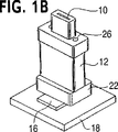
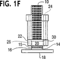
図1Aないし1Fから明らかなように、複数の光ファイバ10がフェルール12内に挿入されている。光ファイバ10と通信すべき光電子デバイス14は、好適には、シリコンベンチまたは補助台座16の上に設けられている。そして、このシリコンベンチ16は、好適には、基板18の上に設けられている。光学的ブロック20は、各光電子デバイス14と対応する光ファイバ10の間に少なくとも1つの光学部品を設ける。光学的ブロック20は、好適には、スペーサ15により光電子デバイス14と離間している。この光学部品は、好適には、光をコリメートする部品、集光する部品、および/または光を均質化する部品を有する。この光学的ブロックは、2つの表面を有するので、2つの光学部品をその表面上に配置することができる。さらに、必要ならば、別の光学的ブロックをこの光学的ブロック20から離して接合すると、別の表面を設けることができる。
【0020】
機械的接続部22により、すでに光電子デバイス14および機械的接続部22と位置合わせされた光学的ブロック20が、光ファイバ10と位置合わせされる。これは、機械的接続部22と光ファイバ10を収容するフェルール12の両方に、位置合わせ用の特徴的形状により実現できる。図示した特別の例においては、この位置合わせ用の特徴的形状は、フェルール12を他のデバイスと位置合わせするためにすでに存在するフェルール内の孔24と、機械的接続部22における位置合わせ孔26とからなる。これらの位置合わせ孔24,26が位置合わせされると、図示しない位置合わせピンがこれらの孔の中に挿入され、位置合わせした状態を維持することができる。
【0021】
機械的接続部と光学的接続部を備えるために別々の構成部品を用いると、いくつかの利点がある。例えば、位置合わせ孔26を機械的接続部22内に設けることにより、光学的特性の観点から選択された材料を用いて、光学的ブロックを形成することができる。例えば、光学的ブロックは、内部に光学部品を形成する上で適当なガラスで形成してもよい。ただし、円筒状の孔をガラスに正確に形成することは困難である。したがって、孔を設ける必要がある場合、すなわち機械的接続部と光学的接続部を単一の部材で構成しようとした場合、この材料も同様に適当なものではない。さらに、機械的接続部が位置合わせピンを受容する必要があるので、ピンを収容するのに十分な大きさを有していなくてはならない。この目的において、ガラスはあまりにも壊れやすい。最後に、デバイスをプリント回路基板または他の電気的接続部に半田付けするときなどに生じる熱に対して、ガラスは耐えることができる。つまり、このシステムは、電気的接続部に表面実装またはプラグ接続することができる。
【0022】
機械的接続部は、同様に、その機能に最も適した材料で形成することができる。機械的接続部22は、同様に、好適には、開口部28を有しており、光は、機械的接続部により干渉されることなく、光電子デバイス14および光ファイバ10の間を伝播することができる。この開口部を設けることにより、光学的特性を損なうことなく、不透明で、熱に対して安定性を有し、孔を正確に簡単に形成できる材料、例えば、ガラス充填プラスチック、セラミック、モールドプラスチックなどの所望する材料で機械的接続部を形成することができる。
【0023】
さらに、図示した特定の実施例において、開口部28は、そのリップ部30以外において、光学的ブロック20を包囲するのに十分な大きさを有するように形成される。このリップ部により、光学的ブロック20の上部と光ファイバの端面の間を適当に離間させることができる。機械的接続部22は、光ファイバと光電子デバイスの間で往復する光の波長に対して透明な材料で形成される場合、開口部28は必要でなくなる。残りの部分がスペーサとして機能する場合、光学的ブロック20を受容するためのカットアウト部が、依然として必要である場合がある。いずれの構成においても、光ファイバ10と光学的ブロック20は、物理的に接触しない。
【0024】
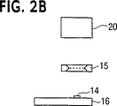
全体の構造物に関する位置合わせについて、図2Aないし図3を参照して説明する。図2Aおよび図2Bは、光学的ブロック20および光電子デバイス14を含む光学的サブアセンブリの位置合わせについて図示する。まず、光電子デバイス14がベンチ16の上に配置される。そして、スペーサ15が用いられる場合、スペーサ15上の基準マークなどの位置合わせ印34が、ベンチ16上の基準マークなどの位置合わせ印32と位置合わせされる。そして半田またはエポキシ樹脂などを用いて、スペーサ15がベンチ16上の所定位置に接合される。シリコンをスペーサとして用い、内部の孔を結晶面に沿ってシリコンをウェットエッチングにより形成した場合、スペーサ15の内側表面上に見られる傾斜が形成される。ウェットエッチングは、スペーサ内に孔を形成する上で単純な方法であるが、例えば、負荷を支持する上で垂直な側壁の方がより有効である場合もある。実質的に垂直な側壁は、ドライエッチングで実現することができる。さらに、セラミック、ガラス、プラスチックなどの他の材料もスペーサ15として用いることができる。スペーサ15が関連波長に対して透明である場合、この孔は必要でなくなる。
【0025】
光学的ブロック20上の基準マークなどの位置合わせ印36が、スペーサ15およびベンチ16の上の対応する印と位置合わせされる。そして半田またはエポキシ樹脂などを用いて、光学的ブロック20がスペーサ15上の所定位置に接合される。光学的ブロック20上の光学部品および位置合わせ印36は、ウェーハ段階で大量生産され、ダイ切断して、個々の光学部品を形成することができる。つまり、光学的ブロック20上のすべての光学部品を位置合わせするために、光学的ブロック20だけを光電子デバイス14と位置合わせすればよい。
【0026】
好適には、スペーサと光学部品は、ウェーハ段階で位置合わせされ、接合され、そして個々のダイを形成するためにダイ切断される。このダイは、その後、ベンチに位置合わせされる。スペーサの位置合わせは、さほど厳格なものではない。すなわち、スペーサが光学的ブロック20と光電子デバイスの間において光を遮らないように、これを位置合わせすればよい。スペーサを光学的ブロックの上に直接的に形成できる場合、別のスペーサ15を用いて、垂直方向により大きく離間させることができる。光学部品およびスペーサの印を形成するプロセスが互いに干渉し合うので、光学部品を光学的ブロック20の底面に配置するとき、別のスペーサを用いることは特に有効である。付言すると、別のスペーサを用いると、より容易に、安定して光電子デバイス14を封止することができる。こうした封止により、湿気などの環境ファクタから光電子デバイス14を保護することができる。
【0027】
近赤外などの特定の波長に対して、光学的ブロック20は、シリコンなどの別の材料で構成することができる。そして、基板、スペーサ、光学的ブロックといった光学的サブアセンブリ内のすべての構成要素は、シリコンなどの同じ材料を用いて構成することができる。これらすべての構成部品を同じ材料で構成することにより、熱膨張係数の差異に起因したこれら構成部品間のストレスを緩和することができる。
【0028】
図3Aおよび3Bに図示するように、光学的ブロック20が機械的接続部22および光ファイバ10に位置合わせされる。光学的ブロック20はすでに光電子デバイス14と位置合わせされているので、簡単のために、光学的ブロック20だけを図示する。図示された特定の具体例において、光学的ブロック20を機械的接続部22に対して非点灯状態で位置合わせすることができる。光学的ブロック20を位置決めしやすくするために、アクセス孔38が機械的接続部に形成される。機械的接続部が光学的ブロックにより包囲されない場合、アクセス孔38は必要ない。
【0029】
光学的ブロック20および機械的接続部22のリップ部30の上にある基準マークおよび/または機械的な照合印を用いて、こうした非点灯状態での位置合わせを行うことができる。リップ部30は、光学的ブロック20を光ファイバ10の端面から所望する距離を隔てた位置に維持する光学的実装表面を提供する。光学的ブロック20と光電子デバイス14は、位置合わせされると、次に、機械的接続部22に接合される。機械的接続部22と、これに接合されたすべての構成部品は、位置合わせ孔24,26により、ハウジング12と位置合わせされ、構造体が完成する。
【0030】
先に説明したような非点灯状態での位置合わせにおいては、位置合わせすべき構成部品上の位置合わせ用の特徴的形状が位置合わせされるが、これに加えて、位置合わせテンプレートを用いて、そして/または機械的接続部に設けたピンを受容するための孔の配置位置を用いて、非点灯状態において位置合わせすることができる。さらに、点灯状態での位置合わせを用いることもできる。
【0031】
別の実施形態が図4に図示されている。この場合、機械的接続部22は、光学的ブロックを包囲せず、むしろ光学ブロック20の上部に配置されている。開口部28および位置合わせ孔26は、同様に、機械的接続部22の一部であるが、他の部材を必要としない。さらに、リップ部が存在しないので、位置合わせ印を機械的接続部22の本体部上に形成してもよい。
【0032】
光学的ブロック20の両面を用いることにより、光電子デバイス14と光ファイバ10の間に光を伝播させる小型のシステムを実現しつつ、光電子デバイス14をさらに離間して配置することができる。このように配置することにより、光電子デバイス間のクロストークを減少させることができる。図4Aで図示するように、光電子デバイスが発光素子であるとき、光学的ブロック20の第1の表面42が光電子デバイス14からの光をコリメートし、偏向する。光学的ブロック20の第1の表面48上にある光学部品46は、光ファイバ10上に光を集光する。明らかなように、光電子デバイスが受光器である場合、これらの光学部品の機能は逆となる。
【0033】
システムが送受信用システムであるとき、すなわち少なくとも1つの発光素子と受光素子を有する場合、光電子デバイスをファイバよりも遠くへ配置できることは、特に有用である。図4Aに示す方向に対して直交する方向において、発光素子と受光素子をさらに離間させることにより、この間隔をさらに広げることができる。こうした構成を図4Bに示し、発光素子50は、受光素子52に対して2つの方向において離間する。これらの構成部品は、依然として、位置合わせ孔24,26の間にあるが、光ファイバ10間よりもさらに離間して、さらに垂直方向においても離間している。このように構成することにより、本来の形状を維持しながら、クロストークを最小限に抑えることができる。さらに、光学的ブロックが機械的接続部よりも大きくない場合でも、このように離間させることができる。
【0034】
本発明の接続部を用いた構成を図5に示し、このとき、光ファイバハウジングを光電子デバイスの平面に対して直交するように配置する。位置合わせ孔24,26を同様に用いて、光ファイバハウジング12と機械的接続部22を位置合わせする。機械的接続部22は、ここでは光学的ブロック20の側面に対して位置合わせされる。光ファイバと光電子デバイス14の間の光を偏向させるために、反射表面60が設けられる。図5に示すように、この反射表面60は、ガラスまたは他の材料で形成することができる。この表面に金属被膜を施して、反射率を上げることもできる。反射表面を有する材料を光学的ブロック20の上部表面に接合することができる。
【0035】
図5に示す特定な具体例において、光電子部品14はVCSELであって、別の光電子部品14’はVCSELが出力するパワーをモニタする。光学的ブロック20上の第1部品62は、VCSELが出力したビームを分割し、その一部をコリメートし、パワーモニタ14’の方へ偏向する。第2の光学部品64は、光学的ブロック20上に形成され、パワーモニタ14’上に光を集光する。こうした構成の詳細については、「回折垂直キャビティの表面発光レーザのパワーモニタおよびシステム」と題する、共通の譲受人に譲渡された同時係属中の米国特許第09/386,280号に開示されている。この特許の全体の開示内容がここに一体のものとして統合される。
【0036】
一方、偏向されなかった光の一部は、第3の光学部品66に伝播し、反射表面60で反射した後、ここで光ファイバに集光される。つまり、本発明によれば、すべての構成部品を同一平面内に配置することなく、ファイバハウジング上にすでに設けてある位置合わせ孔を用いて位置合わせすることができる。これまでVCSELアレイについて説明したが、受光素子も同様に配置することができる。
【0037】
これまでのすべての構成において、光電子デバイスは、その底面を基板16に接合したので、必要な電気的な接続を得るために、ワイヤボンディングすることが必要であった。図6ないし図7Bに示すように、光電子デバイスの上部が光学的ブロックに接合される。一般的な光電子デバイスに対する内部結線が、そのデバイス上で形成されるので、こうしたボンディング手法によれば、ワイヤボンディングを使用しないで済ますことができ、延いてはより小型の内部血線を実現できる。
【0038】
図6に示すように、可撓信号リード72と可撓接地リード74の1組の可撓リードを用いて、光電子デバイス14を内部結線することができる。内部結線スペーサ70は、先のスペーサ15と同じ機能を果たすが、光電子部品14と可撓信号リード72を接続するための内部結線配線をさらに有する。空間的に可能であれば、可撓接地リード74に対する内部結線配線を内部結線スペーサ70上に同様に形成してもよい。さもなければ、図6に示すように、可撓接地リード74を光電子デバイスの底面に固定する必要がある。図6の別の構成部品として示すように、内部結線スペーサ70を光学的スペーサ20と一体に形成することができる。光電子デバイスは、好適には、ヒートシンク78の上に取りつけられる。つまり、上述のワイヤボンド構造に接続するためには必要となる追加的なハウジングを用いることなく、プリント回路基板やフレックス回路などの電気的接続部に、このモジュールを表面実装、またはプラグ接続することができる。
【0039】
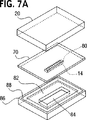
図7Aおよび7Bに示すように、ワイヤボンドを必要としない別の構成によれば、同様に内部結線スペーサ70が設けられ、光電子デバイス、すなわちここではVCSELアレイが接合される。図7Aおよび7Bの別の構成部品として図示するように、内部結線スペーサ70を光学的ブロック20と一体に形成してもよい。光電子デバイス14を可撓リードに接続する代わりに、内部結線スペーサ70は、その底面に形成され、光電子デバイス14から延びる金属ライン80を有する。好適には、セラミックのチップ担体86は、光電子デバイス14を内部に収容するための孔84を有する。チップ担体86は、好適には、一般的な任意の接着剤などの封止リング88を用いてスペーサ80に固定される。
【0040】
またチップ担体86は、金属ライン80をチップ担体の底面などを介して外部へ接続するためのビアを含む接続領域を有する。これは、例えば、チップ担体を貫通する金属で被膜された孔90により実現できる。したがって、上述のワイヤボンド構造に接続するためには必要となる追加的なハウジングを用いることなく、プリント回路基板やフレックス回路などの電気的接続部に、このモジュールを表面実装、またはプラグ接続することができる。図7Aおよび7Bに示す構成において、光電子デバイスに対する必要なすべての接続は、デバイスの上面にあるものとしたが、同様に、接地接続を底面に形成してもよい。
【0041】
図6ないし図7Bに示すように、関連する波長に対して透明生を有するスペーサを放射経路上で用いた場合、スペーサは、その上に形成された光学部品を有していてもよい。例えば、スペーサおよび光学的ブロックが同じ材料を用いて形成された場合、両者間に光学的接続部は存在しない。つまり、スペーサの底面を第2の光学的表面として利用できる。底面に接合された場合、光電子デバイスをこの底面から多少取り除いていもよく、例えば、接合材料からなる十分厚い層を積層することができる。別のスペーサを用いない場合も同様に、光学的ブロックが2つの表面を有するように、このボンディング間隔を有する光学的ブロックの底面に光電子デバイスを固定することができる。スペーサと光学的ブロックが異なる材料で構成される場合、光学部品はスペーサのいずれか一方の表面上に形成できる。当然に、追加的な光学的ブロックを接合して、必要な表面を得ることができるが、システムの厚みがこれに比例して厚くなる。
【0042】
なお、特定の実施形態に関して説明した個別のすべての構成部品が他の構成においても用いることができることに留意されたい。例えば、図6および図7Bに示す光電子デバイス14は、図1および図2Aに示す光学的ブロックの底面に接合することができる。
【0043】
本発明について、特定の用途に関する例示的な実施形態を参照しながら説明したが、本発明はこれに限定されないことを理解されたい。当業者がここに開示した内容を参照すれば、さらなる変形例、変更例、および過度の試験を実施することなく、本発明が重要な意義を与える追加的な分野、および本発明の範疇に入る実施の形態を思いつくことができる。すなわち、本発明の範疇は、ここに開示した実施例ではなく、添付のクレームおよび法的な均等物をもって判断する必要がある。
【図面の簡単な説明】
【図1A】 図1Aは、ハウジングおよび光電子デバイス内の光ファイバに関連する本発明の接続部の分解垂直方向斜視図である。
【図1B】 図1Bは、図1Aに示すシステムの垂直方向斜視図である。
【図1C】 図1Cは、図1Bに示すシステムの内部形状を示す側面図である。
【図1D】 図1Dは、同様に、図1Bに示すシステムの内部形状を示す分解正面図である。
【図1E】 図1Eは、図1Bに示すシステムの平面図である。
【図1F】 図1Fは、図1Bに示すシステムの正面図である。
【図2A】 図2Aは、本発明の光学的サブアセンブリの分解垂直方向斜視図である。
【図2B】 図2Bは、図2Aの分解側面図である。
【図3A】 図3Aは、本発明に係る光ファイバハウジングおよび接続部の分解斜視図である。
【図3B】 図3Bは、図3Aの分解側面図である。
【図4A】 図4Aは、本発明の別の実施形態による光学的接続部の正面図である。
【図4B】 図4Bは、光電子デバイスの位置合わせ孔を示す平面図ある。
【図5】 図5は、本発明の別の実施形態による光学的接続部の側部断面図である。
【図6】 図6は、本発明の別の実施形態による光学的サブアセンブリの側部断面図である。
【図7A】 図7Aは、本発明の別の好適な実施形態による光学的サブアセンブリの分解垂直方向斜視図である。
【図7B】 図7Bは、図7Aに示す構成の分解側面図である。
【符号の説明】
10…光ファイバ、12…フェルール、14…光電子デバイス、15,70…スペーサ、16…シリコンベンチ、18,82…基板、20…光学的ブロック、22…機械的接続部、24,26…位置合わせ孔、28…開口部、30…リップ部、34,36…位置合わせ印、38…アクセス孔、50…発光素子、60…反射表面、72…可撓信号リード、74…可撓接地リード、78…ヒートシンク、86…チップ担体、88…封止リング。[0001]
(Field of Invention)
The present invention relates to optical subassemblies having optical fibers, and more particularly to methods of use in optical fiber communication systems.
[0002]
(Description of related technology)
There are many ways to couple optoelectronic devices and optical fibers together. In the conventional method for realizing this, the optoelectronic device is directly brought into close contact with the end face of the optical fiber and coupled. In such butt coupling, it is necessary to perform active alignment in order to achieve a desired level coupling efficiency. Furthermore, when using butt coupling, the light beam cannot be modulated. Finally, such butt coupling requires the optoelectronic devices to be placed close together, depending on the spacing of the optical fibers, which increases crosstalk.
[0003]
Another approach for coupling optical fibers and optoelectronic devices uses short optical fibers that are coupled to optical fibers. This allows a surface emitting optoelectronic device to be coupled to an optical fiber, but still requires alignment in the lit state. In the alignment method in the passive alignment proposed so far, for example, a ferrule that accommodates an optical fiber, an optical coupling device that includes an optical component, and a substrate that includes an optoelectronic device need to be aligned. Make holes in all components. A pin is inserted into the hole so that all components are aligned. Thus, single point alignment may not be accurate enough for all applications. Moreover, the material used for the optical coupling device is limited when it is necessary to drill holes. Finally, in such alignment, all components need to be placed linearly.
[0004]
(Summary of the Invention)
The present invention thus relates to an optical subassembly that substantially overcomes one or more of the disadvantages or deficiencies of the related art.
[0005]
This and other advantages include an optoelectronic device, an optical block, and a spacer spaced apart from the optical block forming a space between the optoelectronic device and the optical block, the optoelectronic device, the optical block, and The spacer is realized by providing an integrated active optical system that is aligned and joined together.
[0006]
The spacer and the optical block may be aligned and bonded at the wafer stage prior to die cutting. The system further includes a substrate, and the bottom surfaces of both the optoelectronic device and the spacer are bonded to the substrate. The optoelectronic device may be bonded to the substrate at the wafer stage prior to die cutting. The upper surface of the optoelectronic device may be bonded to a spacer, and the spacer may further have an internal wiring. The optoelectronic device may be bonded to the spacer at the wafer stage prior to die cutting. The substrate, optical block, and spacer can all be formed of silicon. This system can be surface mounted to electrical connections.
[0007]
The optoelectronic device may have at least two optoelectronic devices. The at least two optoelectronic devices may be a light source and a light receiver.
[0008]
The above and other objects include a housing having an optical fiber, an optoelectronic device, and an optical block having two surfaces, each surface having optical components thereon, the optical block comprising: This is accomplished by coupling light between the optoelectronic device and the optical fiber and providing a system in which the housing, optoelectronic device, and optical block are integrally formed.
[0009]
The optoelectronic device may include at least two optoelectronic devices, and the optical fiber may include at least two optical fibers. In at least one direction, the at least two optoelectronic devices may be spaced apart from each other longer than the distance that the at least two optical fibers are spaced apart from each other.
[0010]
The at least two optoelectronic devices may be spaced apart from each other in at least two directions, and the at least two optoelectronic devices may be separated from each other in each direction. The at least two optoelectronic devices may have a light source and a light receiver.
[0011]
The system may further include a spacer block between the optical block and the optoelectronic device. The system further includes a substrate, and the bottom surfaces of both the optoelectronic device and the spacer are bonded to the substrate. The upper surface of the optoelectronic device may be bonded to a spacer, and the spacer may further include an internal connection wiring.
[0012]
The optical axis of the optical fiber and the optical axis of the optoelectronic device may form an angle. The system may further include a reflective surface that deflects light between the optoelectronic device and the optical fiber. At least one optical component on the optical block may homogenize the light. The system may be surface mounted for electrical connections. The optical components on the optical block may be formed at the wafer stage.
[0013]
The above and other objects comprise an optoelectronic device, an optical block having at least one optical component, and a sealing structure surrounding the optoelectronic device, the optoelectronic device, the optical block, and the sealing structure This is realized by providing a system in which is integrated.
[0014]
The system may be surface mounted for electrical connections. The system may further include a spacer between the optical block and the optoelectronic device. You may comprise a sealing structure from the optical block and the bottom face of a spacer. The optical component may be formed on the spacer.
[0015]
The system may further include a substrate that receives the optoelectronic device. You may comprise a sealing structure from the optical block and the bottom face of a spacer. The system may further include a spacer block between the optical block and the optoelectronic device. The sealing structure can be composed of the optical block and the bottom surface of the spacer. The substrate may further have vias extending through the substrate for connecting the optoelectronic device to other systems.
[0016]
The optoelectronic device is in contact with a substrate, which can function as a heat sink for the optoelectronic device.
[0017]
These and other objects of the present invention will be more readily understood from the following detailed description. However, since various modifications and variations within the spirit and scope of the present invention will become apparent to those skilled in the art upon review of this detailed description, the following detailed description and specific examples are illustrative of the present invention. It should be understood that the preferred embodiments are suggested and merely exemplary.
[0018]
(Detailed description of preferred embodiments)
The above and other objects, aspects and advantages will be described with reference to the drawings.
[0019]
As is apparent from FIGS. 1A to 1F, a plurality of
[0020]
The
[0021]
There are several advantages to using separate components to provide a mechanical connection and an optical connection. For example, by providing the
[0022]
The mechanical connection can likewise be formed of a material most suitable for its function. The
[0023]
Further, in the particular embodiment illustrated, the
[0024]
The alignment with respect to the entire structure will be described with reference to FIGS. 2A to 3. 2A and 2B illustrate the alignment of an optical subassembly that includes the
[0025]
Alignment marks 36 such as fiducial marks on the
[0026]
Preferably, the spacers and optical components are aligned, bonded and die cut to form individual dies at the wafer stage. This die is then aligned to the bench. The alignment of the spacers is not very strict. That is, the spacers may be aligned so that they do not block light between the
[0027]
For certain wavelengths, such as near infrared, the
[0028]
The
[0029]
Such a non-lighting alignment can be performed using fiducial marks and / or mechanical verification marks on the
[0030]
In the alignment in the non-lighting state as described above, the characteristic shape for alignment on the component to be aligned is aligned, but in addition to this, using the alignment template, And / or it can align in a non-lighting state using the arrangement position of the hole for receiving the pin provided in the mechanical connection part. Furthermore, alignment in the lighting state can also be used.
[0031]
Another embodiment is illustrated in FIG. In this case, the
[0032]
By using both sides of the
[0033]
It is particularly useful to be able to place optoelectronic devices farther than the fiber when the system is a transmission and reception system, i.e. having at least one light emitting element and light receiving element. By further separating the light emitting element and the light receiving element in the direction orthogonal to the direction shown in FIG. 4A, this interval can be further increased. Such a configuration is shown in FIG. 4B, and the
[0034]
FIG. 5 shows a configuration using the connection portion of the present invention, and at this time, the optical fiber housing is arranged so as to be orthogonal to the plane of the optoelectronic device. The alignment holes 24 and 26 are similarly used to align the
[0035]
In the specific example shown in FIG. 5, the
[0036]
On the other hand, a part of the light that has not been deflected propagates to the third
[0037]
In all the configurations so far, since the bottom surface of the optoelectronic device is bonded to the
[0038]
As shown in FIG. 6, the
[0039]
As shown in FIGS. 7A and 7B, according to another configuration that does not require wire bonding, an
[0040]
The
[0041]
As shown in FIGS. 6-7B, when a spacer having a transparency with respect to the relevant wavelength is used on the radiation path, the spacer may have an optical component formed thereon. For example, if the spacer and the optical block are formed using the same material, there is no optical connection between them. That is, the bottom surface of the spacer can be used as the second optical surface. When bonded to the bottom surface, the optoelectronic device may be somewhat removed from the bottom surface, for example, a sufficiently thick layer of bonding material can be laminated. Similarly, if no separate spacer is used, the optoelectronic device can be secured to the bottom surface of the optical block having this bonding spacing so that the optical block has two surfaces. When the spacer and the optical block are made of different materials, the optical component can be formed on either surface of the spacer. Of course, additional optical blocks can be joined to obtain the required surface, but the thickness of the system increases proportionally.
[0042]
It should be noted that all the individual components described with respect to a particular embodiment can be used in other configurations. For example, the
[0043]
Although the invention has been described with reference to exemplary embodiments for particular applications, it should be understood that the invention is not limited thereto. With reference to what is disclosed herein by those skilled in the art, additional variations, modifications, and additional fields in which the present invention has significant significance and without departing from undue testing will fall within the scope of the present invention. Embodiments can be conceived. In other words, the scope of the present invention should be determined by the appended claims and legal equivalents, not by the embodiments disclosed herein.
[Brief description of the drawings]
FIG. 1A is an exploded vertical perspective view of a connection of the present invention associated with an optical fiber in a housing and optoelectronic device.
FIG. 1B is a vertical perspective view of the system shown in FIG. 1A.
FIG. 1C is a side view showing the internal shape of the system shown in FIG. 1B.
FIG. 1D is an exploded front view showing the internal shape of the system shown in FIG. 1B, similarly.
FIG. 1E is a plan view of the system shown in FIG. 1B.
FIG. 1F is a front view of the system shown in FIG. 1B.
FIG. 2A is an exploded vertical perspective view of the optical subassembly of the present invention.
FIG. 2B is an exploded side view of FIG. 2A.
FIG. 3A is an exploded perspective view of an optical fiber housing and a connecting portion according to the present invention.
FIG. 3B is an exploded side view of FIG. 3A.
FIG. 4A is a front view of an optical connection according to another embodiment of the present invention.
FIG. 4B is a plan view showing alignment holes of the optoelectronic device.
FIG. 5 is a side cross-sectional view of an optical connection according to another embodiment of the present invention.
FIG. 6 is a side cross-sectional view of an optical subassembly according to another embodiment of the invention.
FIG. 7A is an exploded vertical perspective view of an optical subassembly according to another preferred embodiment of the present invention.
FIG. 7B is an exploded side view of the configuration shown in FIG. 7A.
[Explanation of symbols]
DESCRIPTION OF
Claims (24)
光電子デバイス(14)と、
光学的ブロック(20)と、
光学的ブロック(20)と離間したスペーサ(15)とを備え、
このスペーサ(15)は、集積化された能動的な光学システムの光学経路に沿って、光電子デバイス(14)と光学的ブロック(20)の間に空間を形成し、
このスペーサ(15)は、光学的ブロック(20)と光電子デバイス(14)の間にあり、
光電子デバイス(14)、光学的ブロック(20)、およびスペーサ(15)は、位置合わせされ、一体に接合され、
スペーサ(15)と光学的ブロック(20)は、光学的ブロック(20)がダイ切断される前のウェーハ段階で位置合わせされ、接合されることを特徴とするシステム。An integrated active optical system comprising:
An optoelectronic device (14);
An optical block (20);
An optical block (20) and a spaced spacer (15);
This spacer (15) forms a space between the optoelectronic device (14) and the optical block (20) along the optical path of the integrated active optical system,
This spacer (15) is between the optical block (20) and the optoelectronic device (14),
The optoelectronic device (14), the optical block (20), and the spacer (15) are aligned and joined together,
The system characterized in that the spacer (15) and the optical block (20) are aligned and bonded at the wafer stage before the optical block (20) is die cut.
スペーサ(15)は、光電子デバイス(14)を完全に包囲することを特徴とするシステム。The system of claim 1, comprising:
A system characterized in that the spacer (15) completely surrounds the optoelectronic device (14).
基板(18)をさらに有し、
光電子デバイス(14)およびスペーサ(15)の両方の底面が基板(18)と接合されることを特徴とするシステム。The system of claim 1, comprising:
A substrate (18);
A system characterized in that the bottom surfaces of both the optoelectronic device (14) and the spacer (15) are bonded to the substrate (18).
光電子デバイス(14)は、光学的ブロック(20)がダイ切断される前のウェーハ段階で、基板(18)に接合されることを特徴とするシステム。The system according to claim 3, wherein
A system characterized in that the optoelectronic device (14) is bonded to the substrate (18) at the wafer stage before the optical block (20) is die cut.
光電子デバイス(14)の上面がスペーサ(70)に接合され、
スペーサ(15)は、内部結線配線(80)をさらに有することを特徴とするシステム。The system of claim 1, comprising:
The upper surface of the optoelectronic device (14) is bonded to the spacer (70);
The spacer (15) further includes an internal wiring (80).
光電子デバイス(14)は、光学的ブロック(20)がダイ切断される前のウェーハ段階で、スペーサ(70)に接合されることを特徴とするシステム。6. The system according to claim 5, wherein
The system characterized in that the optoelectronic device (14) is bonded to the spacer (70) at the wafer stage before the optical block (20) is die cut.
光電子デバイス(14)を受容するための凹部(84)を含む基板(82)をさらに有することを特徴とするシステム。6. The system according to claim 5, wherein
The system further comprising a substrate (82) including a recess (84) for receiving an optoelectronic device (14).
このシステムは、電気的な接続部に対して表面実装されることを特徴とするシステム。The system of claim 1, comprising:
The system is surface mounted to an electrical connection.
光電子デバイス(14)は、少なくとも2つの光電子デバイス(14)を有することを特徴とするシステム。The system of claim 1, comprising:
The optoelectronic device (14) comprises at least two optoelectronic devices (14).
少なくとも2つの光電子デバイス(14)は、発光源と受光部を有することを特徴とするシステム。10. The system according to claim 9, wherein
The system characterized in that at least two optoelectronic devices (14) comprise a light emitting source and a light receiving part.
少なくとも2つの光電子デバイス(14)は、同一の光電子デバイスのアレイを有することを特徴とするシステム。10. The system according to claim 9, wherein
The system characterized in that at least two optoelectronic devices (14) have an array of identical optoelectronic devices.
光ファイバ(10)を有するハウジング(12)と、
光電子デバイス(14)と、
2つの平行な表面(42,48)を有する光学的ブロック(20)とを備え、
各表面(42,48)は、光学部品をその上に有し、
光学的ブロック(20)は、光電子デバイス(14)および光ファイバ(10)の間において光をカップリングし、
このシステムは、ハウジング(12)と光学的ブロック(20)の間に接続部(22)を有し、
ハウジング(12)は、接続部(20)に対して挿入可能で、かつ取り外し可能で、
接続部(20)は、光電子デバイス(14)および光学的ブロック(20)の間の位置合わせを行い、
光学的ブロック(20)上の光学部品は、ウェーハ段階で形成されることを特徴とするシステム。A system,
A housing (12) having an optical fiber (10);
An optoelectronic device (14);
An optical block (20) having two parallel surfaces (42, 48),
Each surface (42, 48) has optical components thereon,
The optical block (20) couples light between the optoelectronic device (14) and the optical fiber (10),
The system has a connection (22) between the housing (12) and the optical block (20),
The housing (12) is insertable and removable with respect to the connection (20),
The connection (20) performs alignment between the optoelectronic device (14) and the optical block (20),
A system characterized in that the optical components on the optical block (20) are formed at the wafer stage.
光電子デバイス(20)は、少なくとも2つの光電子デバイスを有し、
光ファイバ(14)は、少なくとも2つの光ファイバを有することを特徴とするシステム。The system of claim 12, comprising:
The optoelectronic device (20) comprises at least two optoelectronic devices,
The system characterized in that the optical fiber (14) comprises at least two optical fibers.
少なくとも1方向において、少なくとも2つの光ファイバ(10)が互いに離間する距離よりも長く、少なくとも2つの光電子デバイス(14)は、互いに離間することを特徴とするシステム。The system of claim 12, comprising:
A system characterized in that, in at least one direction, at least two optical fibers (10) are longer than the distance between them, and at least two optoelectronic devices (14) are separated from each other.
少なくとも2方向において、少なくとも2つの光ファイバ(10)が互いに離間する距離よりも長く、少なくとも2つの光電子デバイス(14)は、それぞれの方向において互いに離間することを特徴とするシステム。14. The system according to claim 13, wherein
A system characterized in that, in at least two directions, at least two optical fibers (10) are longer than the distance between them, and at least two optoelectronic devices (14) are separated from each other in each direction.
少なくとも2つの光電子デバイス(14)は、発光源と受光部を有することを特徴とするシステム。14. The system according to claim 13, wherein
The system characterized in that at least two optoelectronic devices (14) comprise a light emitting source and a light receiving part.
少なくとも2つの光電子デバイス(14)は、同一の光電子デバイスのアレイを有することを特徴とするシステム。14. The system according to claim 13, wherein
The system characterized in that at least two optoelectronic devices (14) have an array of identical optoelectronic devices.
光学的ブロック(20)と光電子デバイス(14)の間にスペーサブロック(15)をさらに有し、
スペーサブロック(15)は、システムの光学経路に沿って、光電子デバイス(14)と光学的ブロック(20)の間に空間を形成することを特徴とするシステム。The system of claim 12, comprising:
A spacer block (15) between the optical block (20) and the optoelectronic device (14);
The spacer block (15) forms a space between the optoelectronic device (14) and the optical block (20) along the optical path of the system.
基板(16)をさらに有し、
光電子デバイス(14)およびスペーサ(15)の両方の底面が基板(16)と接合されることを特徴とするシステム。The system of claim 18, comprising:
A substrate (16),
A system characterized in that the bottom surfaces of both the optoelectronic device (14) and the spacer (15) are bonded to the substrate (16).
光電子デバイス(14)の上面がスペーサ(70)に接合され、
スペーサ(70)は、内部結線配線(80)をさらに有することを特徴とするシステム。The system of claim 18, comprising:
The upper surface of the optoelectronic device (14) is bonded to the spacer (70);
The spacer (70) further comprises an internal wiring (80).
光ファイバ(10)の光学軸と、光電子デバイス(14)の光学軸は、互いにある角度をなすことを特徴とするシステム。The system of claim 12, comprising:
A system characterized in that the optical axis of the optical fiber (10) and the optical axis of the optoelectronic device (14) form an angle with each other.
光電子デバイス(14)と光ファイバ(10)の間にある光を偏向させる反射表面をさらに有することを特徴とするシステム。The system of claim 21, comprising:
The system further comprising a reflective surface for deflecting light between the optoelectronic device (14) and the optical fiber (10).
光学的ブロック(20)上の少なくとも1つの光学部品は、光を均質化することを特徴とするシステム。The system of claim 12, comprising:
A system characterized in that at least one optical component on the optical block (20) homogenizes the light.
このシステムは、電気的な接続部(86)に対して表面実装されることを特徴とするシステム。The system of claim 12, comprising:
The system is characterized in that it is surface mounted to an electrical connection (86).
Applications Claiming Priority (3)
| Application Number | Priority Date | Filing Date | Title |
|---|---|---|---|
| US09/418,022 US6374004B1 (en) | 1999-10-14 | 1999-10-14 | Optical subassembly |
| US09/418,022 | 1999-10-14 | ||
| PCT/US2000/028086 WO2001027676A1 (en) | 1999-10-14 | 2000-10-11 | Optical subassembly |
Publications (2)
| Publication Number | Publication Date |
|---|---|
| JP2003511738A JP2003511738A (en) | 2003-03-25 |
| JP4479875B2 true JP4479875B2 (en) | 2010-06-09 |
Family
ID=23656351
Family Applications (1)
| Application Number | Title | Priority Date | Filing Date |
|---|---|---|---|
| JP2001530631A Expired - Fee Related JP4479875B2 (en) | 1999-10-14 | 2000-10-11 | Optical subassembly |
Country Status (6)
| Country | Link |
|---|---|
| US (2) | US6374004B1 (en) |
| EP (1) | EP1224495A1 (en) |
| JP (1) | JP4479875B2 (en) |
| AU (1) | AU1079001A (en) |
| CA (1) | CA2387538A1 (en) |
| WO (1) | WO2001027676A1 (en) |
Families Citing this family (30)
| Publication number | Priority date | Publication date | Assignee | Title |
|---|---|---|---|---|
| US6374004B1 (en) * | 1999-10-14 | 2002-04-16 | Digital Optics Corporation | Optical subassembly |
| US20020122637A1 (en) * | 2000-12-26 | 2002-09-05 | Anderson Gene R. | Optical transmitter, receiver or transceiver module |
| JP2002202440A (en) * | 2000-12-28 | 2002-07-19 | Japan Aviation Electronics Industry Ltd | Structure and method of mounting optical module |
| AUPR245701A0 (en) * | 2001-01-10 | 2001-02-01 | Silverbrook Research Pty Ltd | An apparatus (WSM10) |
| US6771860B2 (en) * | 2001-06-29 | 2004-08-03 | Xanoptix, Inc. | Module mounted aligning optical connector |
| US6643420B2 (en) * | 2001-12-28 | 2003-11-04 | Digital Optics Corp. | Optical subassembly |
| US20030210873A1 (en) * | 2002-05-09 | 2003-11-13 | Moretti Anthony L. | Passive alignment connection for fiber optics incorporating VCSEL emitters |
| US6793407B2 (en) * | 2002-09-25 | 2004-09-21 | International Business Machines Corporation | Manufacturable optical connection assemblies |
| US6863453B2 (en) * | 2003-01-28 | 2005-03-08 | Emcore Corporation | Method and apparatus for parallel optical transceiver module assembly |
| JP2004246279A (en) * | 2003-02-17 | 2004-09-02 | Seiko Epson Corp | Optical module and its manufacturing method, optical communication device, optical and electric mixed integrated circuit, circuit board, electronic equipment |
| CN100392460C (en) * | 2003-03-13 | 2008-06-04 | 富士通株式会社 | Optical transceiver module and method of manufacturing the module |
| JP4307902B2 (en) * | 2003-05-15 | 2009-08-05 | 日本特殊陶業株式会社 | Optical element mounting package, opto-electric composite mounting wiring board |
| JP4705432B2 (en) * | 2005-03-28 | 2011-06-22 | 富士通コンポーネント株式会社 | connector |
| JP4704126B2 (en) * | 2005-06-23 | 2011-06-15 | 富士通株式会社 | Optical module |
| US20070236591A1 (en) * | 2006-04-11 | 2007-10-11 | Tam Samuel W | Method for mounting protective covers over image capture devices and devices manufactured thereby |
| US8456560B2 (en) * | 2007-01-26 | 2013-06-04 | Digitaloptics Corporation | Wafer level camera module and method of manufacture |
| US8605208B2 (en) * | 2007-04-24 | 2013-12-10 | Digitaloptics Corporation | Small form factor modules using wafer level optics with bottom cavity and flip-chip assembly |
| JP2010525413A (en) * | 2007-04-24 | 2010-07-22 | フレックストロニクス エーピー エルエルシー | Auto focus / zoom module using wafer level optics |
| JP4819000B2 (en) * | 2007-07-11 | 2011-11-16 | 富士通コンポーネント株式会社 | Optical waveguide holding member and optical transceiver |
| DE202007014173U1 (en) * | 2007-10-10 | 2007-12-06 | CCS Technology, Inc., Wilmington | Coupling device for coupling at least one optical waveguide to an optical component |
| JP5302714B2 (en) * | 2009-02-26 | 2013-10-02 | 富士通コンポーネント株式会社 | Optical connector |
| US9419032B2 (en) * | 2009-08-14 | 2016-08-16 | Nanchang O-Film Optoelectronics Technology Ltd | Wafer level camera module with molded housing and method of manufacturing |
| US9297967B2 (en) * | 2010-04-30 | 2016-03-29 | Hewlett Packard Enterprise Development Lp | Device for converting signal |
| TW201439631A (en) * | 2013-04-02 | 2014-10-16 | Hon Hai Prec Ind Co Ltd | Optical fiber connector |
| WO2015142787A1 (en) * | 2014-03-17 | 2015-09-24 | Intuitive Surgical Operations, Inc. | Multi-stage instrument connector |
| JP6677654B2 (en) * | 2014-05-23 | 2020-04-08 | ナノプレシジョン プロダクツ インコーポレイテッドNanoprecision Products, Inc. | Vision-based passive positioning of fiber optic subassemblies for optoelectronic devices |
| JP6245071B2 (en) * | 2014-05-23 | 2017-12-13 | 日立金属株式会社 | Optical transmission module |
| WO2016154229A1 (en) * | 2015-03-22 | 2016-09-29 | Nanoprecision Products, Inc. | Optical bench subassembly having integrated photonic device |
| US10481349B2 (en) | 2015-10-20 | 2019-11-19 | Sony Corporation | Optical path conversion device, optical interface apparatus, and optical transmission system |
| US11022755B2 (en) * | 2018-10-23 | 2021-06-01 | Cudoquanta Florida, Inc. | Demountable edge couplers with micro-mirror optical bench for photonic integrated circuits |
Family Cites Families (12)
| Publication number | Priority date | Publication date | Assignee | Title |
|---|---|---|---|---|
| US5168537A (en) * | 1991-06-28 | 1992-12-01 | Digital Equipment Corporation | Method and apparatus for coupling light between an optoelectronic device and a waveguide |
| US5359208A (en) * | 1993-02-26 | 1994-10-25 | Nippon Sheet Glass Co., Ltd. | Chip package with microlens array |
| US5586207A (en) * | 1993-11-29 | 1996-12-17 | Northern Telecom Limited | Methods and assemblies for packaging opto-electronic devices and for coupling optical fibers to the packaged devices |
| US5790730A (en) * | 1994-11-10 | 1998-08-04 | Kravitz; Stanley H. | Package for integrated optic circuit and method |
| US5781682A (en) | 1996-02-01 | 1998-07-14 | International Business Machines Corporation | Low-cost packaging for parallel optical computer link |
| US5940562A (en) * | 1996-03-12 | 1999-08-17 | Minnesota Mining And Manufacturing Company | Stubless optoelectronic device receptacle |
| US5774614A (en) * | 1996-07-16 | 1998-06-30 | Gilliland; Patrick B. | Optoelectronic coupling and method of making same |
| DE19742895C2 (en) | 1997-09-24 | 1999-10-21 | Siemens Ag | Electro-optical arrangement |
| AU1295799A (en) | 1997-11-07 | 1999-05-31 | Gore Enterprise Holdings, Inc. | Optical subassembly for transmitting an optical signal with a controlled divergence angle and output power |
| US5913002A (en) | 1997-12-31 | 1999-06-15 | The Whitaker Corporation | Optical coupling device for passive alignment of optoelectronic devices and fibers |
| US6374004B1 (en) * | 1999-10-14 | 2002-04-16 | Digital Optics Corporation | Optical subassembly |
| US6406195B1 (en) * | 1999-10-14 | 2002-06-18 | Digital Optics Corporation | Interface between opto-electronic devices and fibers |
-
1999
- 1999-10-14 US US09/418,022 patent/US6374004B1/en not_active Expired - Lifetime
-
2000
- 2000-10-11 AU AU10790/01A patent/AU1079001A/en not_active Abandoned
- 2000-10-11 EP EP00972075A patent/EP1224495A1/en not_active Withdrawn
- 2000-10-11 WO PCT/US2000/028086 patent/WO2001027676A1/en not_active Application Discontinuation
- 2000-10-11 CA CA002387538A patent/CA2387538A1/en not_active Abandoned
- 2000-10-11 JP JP2001530631A patent/JP4479875B2/en not_active Expired - Fee Related
-
2001
- 2001-12-28 US US10/032,911 patent/US6533471B2/en not_active Expired - Fee Related
Also Published As
| Publication number | Publication date |
|---|---|
| JP2003511738A (en) | 2003-03-25 |
| AU1079001A (en) | 2001-04-23 |
| US6374004B1 (en) | 2002-04-16 |
| CA2387538A1 (en) | 2001-04-19 |
| WO2001027676A1 (en) | 2001-04-19 |
| EP1224495A1 (en) | 2002-07-24 |
| US20020094176A1 (en) | 2002-07-18 |
| US6533471B2 (en) | 2003-03-18 |
Similar Documents
| Publication | Publication Date | Title |
|---|---|---|
| JP4479875B2 (en) | Optical subassembly | |
| US7751659B2 (en) | Optical apparatus | |
| US6056448A (en) | Vertical cavity surface emitting laser array packaging | |
| JP3730664B2 (en) | Passive alignment frame using single crystal material | |
| JP4012785B2 (en) | Optical connection device | |
| US7961989B2 (en) | Optical chassis, camera having an optical chassis, and associated methods | |
| US6599032B1 (en) | Transmitter/receiver for optical parallel transmission and board for optical module | |
| US7050678B1 (en) | Optical module, optical element attachment method, and receptacle-fitted optical module | |
| WO2005078490A1 (en) | Optical wiring board and method for manufacturing optical wiring board | |
| US6588945B2 (en) | Interface between opto-electronic devices and fibers | |
| US6685363B2 (en) | Passive self-alignment technique for array laser transmitters and receivers for fiber optic applications | |
| JP2007199461A (en) | Optical module | |
| US7171066B1 (en) | Optical module and optical transmission device | |
| JP2004200399A (en) | Optical module and its manufacturing method | |
| US6643420B2 (en) | Optical subassembly | |
| JP2001343560A (en) | Optical module | |
| US20190011650A1 (en) | Optical coupling member and optical module | |
| US20040247256A1 (en) | Optoelectronic transmission and/or reception arrangement | |
| JP2004534272A (en) | Method of manufacturing optical access unit, optical access unit and fiber optic ferrule module | |
| JP2001111158A (en) | Optical communication module and its manufacturing method | |
| CA2523418C (en) | Package for optoelectronic device on wafer level and associated methods | |
| JP2005222003A (en) | Mount, optical component, optical transmission/reception module, and bidirectional optical communication module | |
| JP2007199122A (en) | Optical module | |
| JPH0588051A (en) | Optical module | |
| JP2000199837A (en) | Optical parallel transmitting transceiver |
Legal Events
| Date | Code | Title | Description |
|---|---|---|---|
| A621 | Written request for application examination |
Free format text: JAPANESE INTERMEDIATE CODE: A621 Effective date: 20060221 |
|
| A977 | Report on retrieval |
Free format text: JAPANESE INTERMEDIATE CODE: A971007 Effective date: 20081110 |
|
| A131 | Notification of reasons for refusal |
Free format text: JAPANESE INTERMEDIATE CODE: A131 Effective date: 20090303 |
|
| A601 | Written request for extension of time |
Free format text: JAPANESE INTERMEDIATE CODE: A601 Effective date: 20090602 |
|
| A602 | Written permission of extension of time |
Free format text: JAPANESE INTERMEDIATE CODE: A602 Effective date: 20090609 |
|
| A601 | Written request for extension of time |
Free format text: JAPANESE INTERMEDIATE CODE: A601 Effective date: 20090703 |
|
| A602 | Written permission of extension of time |
Free format text: JAPANESE INTERMEDIATE CODE: A602 Effective date: 20090710 |
|
| A601 | Written request for extension of time |
Free format text: JAPANESE INTERMEDIATE CODE: A601 Effective date: 20090803 |
|
| A602 | Written permission of extension of time |
Free format text: JAPANESE INTERMEDIATE CODE: A602 Effective date: 20090810 |
|
| A521 | Written amendment |
Free format text: JAPANESE INTERMEDIATE CODE: A523 Effective date: 20090901 |
|
| A131 | Notification of reasons for refusal |
Free format text: JAPANESE INTERMEDIATE CODE: A131 Effective date: 20091013 |
|
| A521 | Written amendment |
Free format text: JAPANESE INTERMEDIATE CODE: A523 Effective date: 20091216 |
|
| TRDD | Decision of grant or rejection written | ||
| A01 | Written decision to grant a patent or to grant a registration (utility model) |
Free format text: JAPANESE INTERMEDIATE CODE: A01 Effective date: 20100209 |
|
| A711 | Notification of change in applicant |
Free format text: JAPANESE INTERMEDIATE CODE: A711 Effective date: 20100210 |
|
| A01 | Written decision to grant a patent or to grant a registration (utility model) |
Free format text: JAPANESE INTERMEDIATE CODE: A01 |
|
| A521 | Written amendment |
Free format text: JAPANESE INTERMEDIATE CODE: A821 Effective date: 20100210 |
|
| A61 | First payment of annual fees (during grant procedure) |
Free format text: JAPANESE INTERMEDIATE CODE: A61 Effective date: 20100309 |
|
| FPAY | Renewal fee payment (event date is renewal date of database) |
Free format text: PAYMENT UNTIL: 20130326 Year of fee payment: 3 |
|
| R150 | Certificate of patent or registration of utility model |
Ref document number: 4479875 Country of ref document: JP Free format text: JAPANESE INTERMEDIATE CODE: R150 Free format text: JAPANESE INTERMEDIATE CODE: R150 |
|
| FPAY | Renewal fee payment (event date is renewal date of database) |
Free format text: PAYMENT UNTIL: 20130326 Year of fee payment: 3 |
|
| S533 | Written request for registration of change of name |
Free format text: JAPANESE INTERMEDIATE CODE: R313533 |
|
| FPAY | Renewal fee payment (event date is renewal date of database) |
Free format text: PAYMENT UNTIL: 20130326 Year of fee payment: 3 |
|
| R350 | Written notification of registration of transfer |
Free format text: JAPANESE INTERMEDIATE CODE: R350 |
|
| FPAY | Renewal fee payment (event date is renewal date of database) |
Free format text: PAYMENT UNTIL: 20140326 Year of fee payment: 4 |
|
| R250 | Receipt of annual fees |
Free format text: JAPANESE INTERMEDIATE CODE: R250 |
|
| R250 | Receipt of annual fees |
Free format text: JAPANESE INTERMEDIATE CODE: R250 |
|
| S111 | Request for change of ownership or part of ownership |
Free format text: JAPANESE INTERMEDIATE CODE: R313113 |
|
| S531 | Written request for registration of change of domicile |
Free format text: JAPANESE INTERMEDIATE CODE: R313531 |
|
| R350 | Written notification of registration of transfer |
Free format text: JAPANESE INTERMEDIATE CODE: R350 |
|
| R250 | Receipt of annual fees |
Free format text: JAPANESE INTERMEDIATE CODE: R250 |
|
| S111 | Request for change of ownership or part of ownership |
Free format text: JAPANESE INTERMEDIATE CODE: R313113 |
|
| R360 | Written notification for declining of transfer of rights |
Free format text: JAPANESE INTERMEDIATE CODE: R360 |
|
| R360 | Written notification for declining of transfer of rights |
Free format text: JAPANESE INTERMEDIATE CODE: R360 |
|
| R371 | Transfer withdrawn |
Free format text: JAPANESE INTERMEDIATE CODE: R371 |
|
| S111 | Request for change of ownership or part of ownership |
Free format text: JAPANESE INTERMEDIATE CODE: R313113 |
|
| R350 | Written notification of registration of transfer |
Free format text: JAPANESE INTERMEDIATE CODE: R350 |
|
| R250 | Receipt of annual fees |
Free format text: JAPANESE INTERMEDIATE CODE: R250 |
|
| R250 | Receipt of annual fees |
Free format text: JAPANESE INTERMEDIATE CODE: R250 |
|
| R250 | Receipt of annual fees |
Free format text: JAPANESE INTERMEDIATE CODE: R250 |
|
| S111 | Request for change of ownership or part of ownership |
Free format text: JAPANESE INTERMEDIATE CODE: R313111 |
|
| R350 | Written notification of registration of transfer |
Free format text: JAPANESE INTERMEDIATE CODE: R350 |
|
| LAPS | Cancellation because of no payment of annual fees |