JP4463879B2 - Method and apparatus for docking and undocking a notebook computer - Google Patents
Method and apparatus for docking and undocking a notebook computer Download PDFInfo
- Publication number
- JP4463879B2 JP4463879B2 JP52363698A JP52363698A JP4463879B2 JP 4463879 B2 JP4463879 B2 JP 4463879B2 JP 52363698 A JP52363698 A JP 52363698A JP 52363698 A JP52363698 A JP 52363698A JP 4463879 B2 JP4463879 B2 JP 4463879B2
- Authority
- JP
- Japan
- Prior art keywords
- notebook computer
- docking station
- docking
- system bus
- common system
- Prior art date
- Legal status (The legal status is an assumption and is not a legal conclusion. Google has not performed a legal analysis and makes no representation as to the accuracy of the status listed.)
- Expired - Fee Related
Links
Images


Classifications
-
- G—PHYSICS
- G06—COMPUTING; CALCULATING OR COUNTING
- G06F—ELECTRIC DIGITAL DATA PROCESSING
- G06F13/00—Interconnection of, or transfer of information or other signals between, memories, input/output devices or central processing units
- G06F13/38—Information transfer, e.g. on bus
- G06F13/40—Bus structure
- G06F13/4063—Device-to-bus coupling
- G06F13/4068—Electrical coupling
- G06F13/4081—Live connection to bus, e.g. hot-plugging
-
- G—PHYSICS
- G06—COMPUTING; CALCULATING OR COUNTING
- G06F—ELECTRIC DIGITAL DATA PROCESSING
- G06F1/00—Details not covered by groups G06F3/00 - G06F13/00 and G06F21/00
- G06F1/16—Constructional details or arrangements
-
- G—PHYSICS
- G06—COMPUTING; CALCULATING OR COUNTING
- G06F—ELECTRIC DIGITAL DATA PROCESSING
- G06F1/00—Details not covered by groups G06F3/00 - G06F13/00 and G06F21/00
- G06F1/16—Constructional details or arrangements
- G06F1/1613—Constructional details or arrangements for portable computers
- G06F1/1632—External expansion units, e.g. docking stations
-
- Y—GENERAL TAGGING OF NEW TECHNOLOGICAL DEVELOPMENTS; GENERAL TAGGING OF CROSS-SECTIONAL TECHNOLOGIES SPANNING OVER SEVERAL SECTIONS OF THE IPC; TECHNICAL SUBJECTS COVERED BY FORMER USPC CROSS-REFERENCE ART COLLECTIONS [XRACs] AND DIGESTS
- Y02—TECHNOLOGIES OR APPLICATIONS FOR MITIGATION OR ADAPTATION AGAINST CLIMATE CHANGE
- Y02D—CLIMATE CHANGE MITIGATION TECHNOLOGIES IN INFORMATION AND COMMUNICATION TECHNOLOGIES [ICT], I.E. INFORMATION AND COMMUNICATION TECHNOLOGIES AIMING AT THE REDUCTION OF THEIR OWN ENERGY USE
- Y02D10/00—Energy efficient computing, e.g. low power processors, power management or thermal management
Landscapes
- Engineering & Computer Science (AREA)
- Theoretical Computer Science (AREA)
- General Engineering & Computer Science (AREA)
- Physics & Mathematics (AREA)
- General Physics & Mathematics (AREA)
- Computer Hardware Design (AREA)
- Human Computer Interaction (AREA)
- Power Sources (AREA)
Description
関連出願の相互参照
本出願は、本出願と同じ日付に出願されたCho等の「METHOD AND APPARATUS FOR DOCKING AND UNDOCKING A NOTEBOOK COMPUTER」と題する米国特許出願第______号に関する。
発明の分野
本発明は、コンピュータ・システムの分野に関する。詳細には、本発明は、ノート型コンピュータのドッキング・ステーションへのドッキングとドッキング・ステーションからのドッキング解除に関する。
発明の背景
現在、ノート型(携帯)コンピュータには、以前はデスクトップ・パーソナル・コンピュータ上でしか得られなかった多数の機能が組み込まれている。ノート型コンピュータに接続されたドッキング・ステーションを使用することによって、ユーザは、通常はデスクトップ・コンピュータでしか得られない様々なサービスにアクセスすることができる。したがって、ノート型コンピュータをドッキング・ステーションに接続するか、あるいは取り付けると、結果として得られるシステムはデスクトップ・コンピュータに類似したものになる。
ノート型コンピュータは通常、ソケット型接続部を使用することによってドッキング・ステーションに接続される。すなわち、ノート型コンピュータは、ドッキング・ステーションに挿入され、このような挿入時には、かみ合いコネクタを使用することによってドッキング・ステーションに接続される。ノート型コンピュータをドッキング・ステーションから係合解除する際、ノート型コンピュータは単にドッキング・ステーションから取り外される。
ノート型コンピュータをドッキング・ステーションに挿入しドッキング・ステーションから取り外す従来技術の方法に関する1つの重要な問題は、ユーザが手動で介入しないかぎり挿入プロセスもあるいは取外しプロセスも実行できないことである。
したがって、他の従来型のドッキングおよびドッキング解除方法は、ユーザが事前に条件付けを行わずにノート型コンピュータをドッキング・ステーションに挿入し、ドッキング・ステーションから取り外すことを可能にする回路を使用する。したがって、ノート型コンピュータ上でアプリケーション・プログラムを実行している場合でも、アプリケーション・プログラムに割り込まずにノート型コンピュータをドッキング・ステーションに挿入するか、あるいはドッキング・ステーションから取り外すことができる。
従来技術のシステムは、ドッキング・チップを含むインタフェースを使用している。このインタフェースは、挿入アルゴリズムおよび取外しアルゴリズムを処理するノート型コンピュータ内に存在する。この従来技術のシステムは、事前条件付けなしでドッキングおよびドッキング解除を可能にするという点で有利であるが、回路構成要素の数が増えるためにノート型コンピュータが複雑になるという欠点を有する。ノート型コンピュータに含まれる回路構成要素が多ければ多いほど、バッテリの消費が多くなり、ノート型コンピュータの製造費が高くなり、ノート型コンピュータが大型になる。
発明の概要
事前条件付けなしでノート型コンピュータをドッキング・ステーションにドッキングする方法および装置について説明する。この装置は、ノート型コンピュータとドッキング・ステーションを相互接続するためにドッキング・ステーション内に位置するインタフェース回路を含む。このインタフェースは、ノート型コンピュータがドッキング・ステーションに挿入されたときにそのことを検出し、それに対応して、ノート型コンピュータとドッキング・ステーションの間に共通システム・バスが結合されるようにスイッチをイネーブルする。インタフェースはまた、ユーザの事前の介入なしにソフトウェアがノート型コンピュータおよびドッキング・ステーションを構成することを可能にするイベントを生成する。
【図面の簡単な説明】
本発明は、以下で与える詳細な説明と、本発明の様々な実施形態の添付の図面からより完全に理解されよう。しかし、この説明および図面は、本発明を特定の実施形態に制限するものとみなされるべきではなく、説明および理解のためのものに過ぎない。
第1図は、本発明のノート型コンピュータおよびドッキング・ステーションのブロック図である。
第2図は、本発明のドッキング・ステーション・コネクタの一実施形態を示す図である。
第3図は、本発明の一実施形態によるドッキング・インタフェース・チップを示す図である。
第4a図は、本発明によるドッキング・ステーション電源の第1の実施形態を示す図である。
第4b図は、本発明によるドッキング・ステーション電源の第2の実施形態を示す図である。
第5図は、本発明の一実施形態によるドッキング状態マシンの状態図である。
第6図は、ノート型コンピュータのドッキングおよびドッキング解除を処理する方法を示す流れ図である。
第7図は、本発明の一実施形態内でアサートされる信号のタイミング図である。
本発明の詳細な説明
ノート型コンピュータをドッキングし、かつドッキング解除する方法および装置について説明する。本発明の以下の詳細な説明では、本発明を完全に理解していただくために、特定のバス・プロトコル、電圧、イベント名、割込み名など多数の特定の詳細について述べる。しかし、当業者には、これらの特定の詳細なしに本発明を実施できることが明らかであろう。他の例では、本発明を曖昧にすることを回避するために周知の構造および装置を詳しく示さずにブロック図形で示す。
発明の概要
本発明は、ユーザの介入を必要としないノート型コンピュータとドッキング・ステーションの間の非事前条件付け自動挿入/取外しプロトコルを提供する。さらに、本発明は、ドッキング・インタフェースがノート型コンピュータ内ではなくドッキング・ステーション内に位置するという点で有利である。
ノート型コンピュータは、ドッキング・ステーションに挿入されると、コネクタを介してドッキング・ステーションに結合される。このコネクタは、ノート型コンピュータとドッキング・ステーションの間に共通信号線を結合するピンを含む。たとえば、コネクタは、ノート型コンピュータとドッキング・ステーションの間に共通システム・バスを接続するために使用される。
この共通システム・バスはスイッチにも結合される。このスイッチは、ドッキング・ステーション内のインタフェース回路によって制御される。ノート型コンピュータがドッキング・ステーション内に挿入されたことをインタフェース回路が検出すると、スイッチが閉じ、ノート型コンピュータの共通システム・バスがドッキング・ステーションに結合される。しかし、共通システム・バス上でトランザクションが行われているので、トランザクションに割り込まずにスイッチを閉じても安全であるとインタフェース回路が判定するまでスイッチは閉じない。したがって、インタフェース回路は、共通システム・バスの制御を要求し、次いでインタフェース回路に制御が与えられた後にスイッチを閉じる。
本発明の一実施形態では、インタフェース回路は、スイッチが閉じた後にドッキング・イベントを生成する。このイベントは、ユーザの事前の介入なしにノート型コンピュータおよびドッキング・ステーションを自動的に構成するソフトウェア・ルーチンによって検出される。たとえば、このソフトウェア・ルーチンは、共通のシステム・バスに結合されたドッキング・ステーション内に、装置に必要な装置ドライバをロードすることができる。
ノート型コンピュータは、ドッキング・ステーションに挿入される際、中断モードである可能性も、あるいは通常モードである可能性もある。本発明の一実施形態では、インタフェース回路が挿入時にノート型コンピュータのモードを検査する。ノート型コンピュータが中断モードである場合、インタフェース回路は、スイッチを閉じドッキング・イベントを生成する前に、ノート型コンピュータを通常モードで再開させる。
ノート型コンピュータは、ドッキング・ステーションにドッキングされた後、中断モードに入ることができる。一実施形態では、インタフェース回路が、ノート型コンピュータが中断モードに入ることを検出し、それによってドッキング・ステーションも中断モードにする。
インタフェース回路はまた、ノート型コンピュータがドッキング・ステーションから取り外されるときにそのことを検出する。インタフェース回路は、ノート型コンピュータのドッキング・ステーションからの物理的な取外しを検知するか、あるいはシステムのユーザまたはソフトウェア・ルーチンからのイジェクト要求を受け取ることによって取外しを検出する。この取外しに応答して、インタフェース回路はまず、ドッキング解除イベントを生成し、これによってソフトウェアは、コンピュータ・システムにノート型コンピュータを取り外す準備をさせる。次いで、インタフェース回路はスイッチを開き共通システム・バスを分離する。
インタフェース回路によってイジェクト要求が検出されたときに、ノート型コンピュータは中断モードである可能性も、あるいは通常モードである可能性もある。一実施形態では、イジェクト要求が検出されたときにノート型コンピュータが中断モードである場合、インタフェース回路は、ドッキング解除イベントを生成しスイッチを開く前に、ノート型コンピュータを通常モードで再開させる。
ソフトウェア・ルーチンは、ドッキング解除イベントを検出すると、ノート型コンピュータを取り外せるようにノート型コンピュータおよびドッキング・ステーションを構成する。ドッキング解除イベントなどのイベントが、挿入時または取外し時にソフトウェア・ルーチンがノート型コンピュータおよびドッキング・ステーションを構成することを可能にするためにインタフェース回路によって生成されることを想起されたい。このようなイベントは、ドッキング・ステーション内のインタフェース回路によって自動的に生成される。したがって、ユーザがドッキングまたはドッキング解除を開始する前に手動で介入する必要はない。
取外しが検出されるときには共通システム・バス上でトランザクションが行われているので、インタフェース回路は、共通システム・バスのキャパシタンスの変化がトランザクションに影響を与えないときにスイッチを開く。インタフェース回路がスイッチを開くのは、システム・バス・クロックの立上りと次のシステム・バス・クロックのセットアップ時間との間の時点である。したがって、スイッチが開いたために共通システム・バス上の信号が変動した場合、信号は次のクロックのセットアップ時間までに安定する。
本発明は、ノート型コンピュータおよびドッキング・ステーションの条件または状態を自動的に検出し、ノート型コンピュータまたはドッキング・ステーションの電力を自動的に制御し、システム・ソフトウェア相互作用に関するイベントを生成し、挿入プロセスまたは取外しプロセス中、あるいはノート型コンピュータが完全に取り付けられている間に相互接続信号を自動的に分離し、イネーブルし、相互接続信号同士が衝突するのを妨げ、資源を見つけ割り付ける。
本発明で参照されるソフトウェア・ルーチンが、コンピュータ・システム内のハードウェアの動作を制御し、様々なプログラミング言語で実装できることに留意されたい。たとえば、このようなソフトウェア・ルーチンは、アセンブリ言語で書かれた基本入出力システム(BIOS)を含むことができる。このソフトウェアはファームウェア、実行時ライブラリ・ルーチン、またはオペレーティング・システム手順として完全に実装することも、あるいは部分的に実装することもできる。
本発明の装置の詳細な説明
第1図は、本発明のシステムの一実施形態のブロック図である。第1図を参照するとわかるように、システムはドッキング・ステーション11とノート型コンピュータ10を含み、ドッキング・ステーション11とノート型コンピュータ10はそれぞれ、点線で分離して示されている。ノート型コンピュータ10とドッキング・ステーション11の間に、この2つの間での信号の電気的接続を容易にするコネクタ12が位置決めされる。ノート型コンピュータ10は、ドッキング・ステーション11のかみ合いコネクタ12に適切に結合されたときに、ドッキング・ステーション内に「取り付けられた」と言われる。
図の実施形態では、ノート型コンピュータ10は、第2レベル(L2)キャッシュ111に結合されたマイクロプロセッサ110を備える。マイクロプロセッサは、メモリ・コントローラおよびブリッジ・チップ113を介してメモリ(DRAM)112およびシステム・バス180と通信する。一実施形態では、マイクロプロセッサ110は、カリフォルニア州Santa ClaraのIntel Corporationによって製造されているIntel Architecture Microprocessor(たとえば、i486プロセッサやPentium(R)プロセッサ)を備える。本明細書で説明する実施形態の場合、システム・バス180は、PCIプロトコルに準拠したバスである。別法として、システム・バス180は、業界標準アーキテクチャ(ISA)バスなど他の周知のプロトコルに準拠することもできる。
ノート型コンピュータ10は入出力コントローラ(図示せず)を備えることもでき、この入出力コントローラはシステム・バス180に結合され、並列ポート、二重シリアル・ポート、リアルタイム・クロック・ユニット、二重プログラム可能割込みコントローラ、DMAコントローラ、メモリ・マッパ、入出力バッファを含む。さらに、ノート型コンピュータ10は、フラット・パネル・ディスプレイまたはCRTとのインタフェースをとるためにPCIバス180に結合されたグラフィックス・コントローラおよびビデオ・フレーム・バッファ(図示せず)を備えることもできる。一実施形態では、PCIバス180にハード・ディスク、フロッピィ・ディスク・ドライブ、キーボード、BIOSコントローラも結合される。これらの構成要素はすべて、よく知られており図示されていない。
PCIクロック信号線181はメモリ・コントローラおよびブリッジ・チップ113からQバッファ121に結合される。さらに、PCI要求許可信号対線REQ/GNT#187はQバッファ121を通るように経路指定される。Qバッファ121はQバッファ・イネーブル信号QDEN#によってイネーブルされ、この信号はドッキング電源回路150によって生成され、信号線193でQバッファ121へ送られる。PCIバス180はQバッファ120に結合され、Qバッファ120は、ドッキング・チップ130によって生成される信号線183上のQバッファ・イネーブル信号QPCIEN#によってイネーブルされる。
Qバッファ120および121は、イネーブルされると、ノート型コンピュータ10とドッキング・ステーション11の間の共通信号をバッファする。Qバッファ120および121はまた、ディスエーブルされるとノート型コンピュータ10とドッキング・ステーション11の各共通信号を分離する。一実施形態では、Qバッファ120および121はスイッチとして働き、ディスエーブルされると、Qバッファ120〜121に結合された信号がトライステートになり、それによってノート型コンピュータ10をドッキング・ステーション11から取り外すことができる。
ドッキング・シーケンス中に、PCI Qバッファ120がイネーブルされる前にドッキング・ステーション11がPCIバス180の制御を得ることができるように、PCIクロック線181およびREQ/GNT#線187は別のQバッファ121を通過する。これについては、以下で詳しく説明する。
一実施形態では、線181上のPCIクロックは、ドッキング・コネクタ12に結合されたメモリ・コントローラおよびブリッジ・チップ113やクロッキング・チップ(図示せず)などの供給源からのポイント・ツー・ポイント信号である。さらに、線181上のPCIクロックは、一次ノート型コンピュータPCIバス180上で動作しているクロックに対して低スキュー関係を有する。
一実施形態では、ドッキング・ステーション11は、ドッキング・ステーション11内のすべての装置に電力を供給する電源150を有する。この種のドッキング・ステーション11は、電源150がAC電源(図示せず)によって動作するという点でデスクトップ・コンピュータと類似している。さらに、一実施形態では、ドッキング・ステーション11の電源状態とノート型コンピュータ10の電源状態は互いに独立している。したがって、たとえば、ノート型コンピュータ10が中断状態である間にドッキング・ステーション11を電源オン状態にすることができる。
中断モードとは電力節約状態であり、システムが使用されていないときにノート型コンピュータ10またはドッキング・ステーション11がかなり少ない電力しか消費しないようにする。ドッキング・ステーション11またはノート型コンピュータ10内に実装できるいくつかの中断モードがある。たとえば、「電源オン中断」モードは、リアルタイム・クロック(RTC)を除くシステム内のすべてのクロックをディスエーブルする。この状態で消費される電力は、システム内の漏れ電力だけである。電源オン中断モードからシステムを再開させるときには、単にクロックが再開される。
「DRAM保存後中断」モードは、電源管理論理、メモリ・リフレッシュ論理、フレーム・バッファ・リフレッシュ論理を除くすべての装置への電力をオフにする。DRAM保存後中断モードを呼び出す前に、システム内の各装置のコンテキストをDRAMに保存しなければならない。DRAM保存後中断モードからシステムを再開させるときには、すべての装置をリセットし、各装置のコンテキストを再生しなければならない。
「ディスク保存後中断」モードは、コンピュータ・システムのコンテキスト全体を非揮発性メモリ(たとえば、ハード・ディスク)に保存し、システム全体への電力をオフにする。ディスク保存後中断モードを終了するときには、コンピュータ・システム内のすべての装置に電力を再供給し、リセットし、ハード・ディスク上に保存されているコンテキストを再生しなければならない。
前述のように、一実施形態の場合、ノート型コンピュータ10とドッキング・ステーション11は互いに独立の電力モードを呼び出すことができる。したがって、ノート型コンピュータ10またはドッキング・ステーション11はいつでも、一方の中断モードに入ることができる。
他の実施形態では、ドッキング・ステーション11は携帯型のドッキング・ステーションであり、ドッキング・ステーション電源150はノート型コンピュータ電源160またはドッキング・ステーション自体の内部バッテリ(図示せず)によって動作する。この種のドッキング・ステーションの場合、ドッキング・ステーション11の電力モードはノート型コンピュータ10の電力モードに従う。したがって、ノート型コンピュータ電源160がオンであるとき、ドッキング電源150もオンである。ノート型コンピュータ10が中断モードのときは、ドッキング・ステーション11も中断モードである。
デスクトップ型のドッキング・ステーションの場合、ドッキング・ステーション電源150はコネクタ12上のピンに電力を供給することができる。ノート型コンピュータ10は、ドッキング・ステーション11内に取り付けられたときにこのピンを使用してノート型コンピュータ・バッテリ(図示せず)を充電する。
一実施形態では、ドッキング・ステーション11は、3.3Vまたは5Vで動作しているノート型コンピュータ10にドッキングすることができる。この実施形態では、ドッキング・ステーション電源150はドッキング・ステーション内の構成要素に5V(線188上のDS_VCC)を供給する。ドッキング・ステーション電源150はまた、ノート型コンピュータ10とのインタフェースをとるために必要に応じて5V信号を3.3V信号(線188上のQVCC)に変換する。ドッキング・ステーション電源150はさらに、ドッキング・ステーションの電力が許容公差内であることを示す信号を線191上に供給し、ノート型コンピュータの電力が許容公差内であることを示す信号をドッキング・チップ130への線192上に供給する。ドッキング・ステーション電源150については、第4a図および第4b図を参照して以下で詳しく論じる。
ドッキング・コネクタ12はノート型コンピュータ10とドッキング・ステーション11を接続する。ドッキング・コネクタ12はいくつかのピンを含み、これらのピンはノート型コンピュータ10とドッキング・ステーション11の間で通信を行うために使用される。第1図に示したドッキング・ステーション11内の信号線については、ドッキング・コネクタ12、ドッキング・チップ130、ドッキング電源150を参照して以下で詳しく論じる。
第2図は、ドッキング・コネクタ12の一実施形態を示し、この場合、ドッキング・コネクタ12のノート型コンピュータ側はメス型コネクタを備え、ドッキング・コネクタ12のドッキング・ステーション側はオス型コネクタを備える。任意の周知のコネクタ・タイプを使用して、本発明の範囲から逸脱せずにコネクタ12を実装できることを理解されたい。さらに、ドッキング・コネクタ12のノート型コンピュータ側はピンを備え、ドッキング・コネクタのドッキング・ステーション側はソケットを備えることができる。
コネクタに含まれるピン20b〜26bおよびソケット20a〜26aは、ノート型コンピュータとドッキング・ステーションの間に信号を結合するために使用される。CD1#ピン20bおよびCD2#ピン26bはコネクタ検出ピンである。コネクタ検出ピンは、ノート型コンピュータがドッキング・ステーション内に適切に挿入されたときにそのことを検出するために使用される。「#」はアクティブ・ロー信号を示す。
コネクタ検出ピンがドッキング・コネクタ12のそれぞれの端部に位置決めされていることによってこの検出が容易になる。ドッキング・ステーション側のCD1#20bピンとCD2#26bピンが共にノート型コンピュータ側のソケット20aおよび26a内に適切に挿入されると、接続検出イベントが生成される。このイベントは、ノート型コンピュータがドッキング・ステーション内に取り付けられたことをドッキング・チップ130に示す。
一実施形態では、ドッキング・ステーション側のCD1#20bピンおよびCD2#26bピンが他のピンよりも短いことに留意されたい。これは、コネクタ検出イベントが適切に生成されることを容易にするもう1つの特徴である。CD1#20aおよびCD2#26aピンの方が長さが短いので、より長いピン21b〜25bがすべてソケット21a〜25aに挿入されないかぎりCD1#20aおよびCD2#26aピンはソケット20aおよび26aに挿入されない。したがって、コネクタ検出イベントは、すべてのピン20a〜26aがソケット20a〜26aに挿入された後に生成される。ドッキング・ステーション側がソケット型接続部を備える代替実施形態として、ドッキング・ステーション側のCD1#20b信号およびCD2#26b信号はピンではなく、より短いソケットに対応する。本発明の代替実施形態が、上記よりも多いか、あるいは少ない数の接続検出信号を有するコネクタ12を含み、これらの信号が他の信号ピンおよびソケットに対して任意の長さのピンまたはソケットに対応することを理解されたい。さらに、代替実施形態は、コネクタのかみ合い部分が適切に位置合わせされたときに開き、かつ閉じるスイッチなど、挿入を検出する他の方法を含む。
より長いピン21b〜25bは、ノート型コンピュータ10とドッキング・ステーション11の間に結合される他の信号を示す。GND接続25a〜bは、ノート型コンピュータ10とドッキング・ステーション11の両方によって使用される接地平面を表す。一実施形態では、GNDピン25bは常に、他のピンよりも前にソケット25aに挿入される。したがって、接地平面は他の信号が接続される前に確立され、システムを静電放電(ESD)から保護する。
NB_SW信号線24a〜bは、ノート型コンピュータ10からの5V電力信号をドッキング・ステーション11に接続する。次いで、ドッキング・ステーションが電力に関してノート型コンピュータに依存する第2のタイプのドッキング・ステーション電源の場合、上記の5V電力信号はドッキング電源150に経路指定される。
QVCC接続23a〜bはノート型コンピュータ10内のQバッファ120および121用のバイアス電圧信号線である。QVCC信号はドッキング・ステーション11内の電源150によって生成され、ピン23b上でコネクタ12を通るように経路指定され、Qバッファ120〜121へ送られる。
バッテリ充電(BAT_CH)接続22a〜22bはバッテリ充電信号線であり、ノート型コンピュータ・バッテリ170を充電するためにドッキング・ステーション電源150から送られる。
他の信号21a〜bは、ノート型コンピュータ10とドッキング・ステーション11の間に結合されるバス信号および論理信号を表す。たとえば、ノート型コンピュータとドッキング・ステーションの間にPCIバス180が結合される。したがって、いくつかのPCI信号がコネクタ12を通るように経路指定される。一実施形態では、コネクタ12を介して送られるPCI信号には、CLK、CLKRUN#、RST#、AD[31:0]、C/BE[3:0]#、PAR、FRAME#、IRDY#、TRDY#、STOP#、LOCK#、DEVSEL#、pREQ#、pGNT#、PCPCI REQA#、PCPCI GNTA#、PERR#、SERR#、INTA[A:D]#の、周知の各信号が含まれる。
ノート型コンピュータ10がISAバスを含む実施形態の場合、同様にISA信号がコネクタ12を通るように経路指定される。ISAサポート信号には、定義済みのISA IRQが含まれる。
一実施形態では、6つのドッキング管理信号がコネクタ12を通るように経路指定される。これらの信号にはNBPWRGD、すなわちノート型コンピュータ「電力良好」信号が含まれる。この信号は、ノート型コンピュータ内の5V電力が許容公差内であることを示す。SUS#信号は、ノート型コンピュータが中断されており、ドッキング・ステーション側で5V電力が許容公差内であることを示す。QDEN#信号およびQPCIEN#信号は、ノート型コンピュータ10上のQバッファ120および121をイネーブルするために使用される。DCKINTR#はドッキング・ステーション割込みであり、ドッキング・イベントを知らせるために使用され、SRBTN#信号は、ノート型コンピュータ10を中断モードから再開させるためにドッキング・チップ130によって生成される。
ドッキング・ステーション・コネクタ12は、受動有線信号用のいくつかのピンも含み、これらの受動有線信号は入力装置と出力装置の間の通信を容易にするために使用される。たとえば、LPTポート信号およびCOMポート信号がコネクタ12を通るように経路指定される。さらに、必要に応じてキーボード信号、マウス信号、フロッピィ・ドライブ信号、陰極線管(CRT)信号、電話信号、マイクロフォン信号、スピーカ信号がコネクタ12を通るように経路指定される。本明細書で述べる信号よりも多いか、あるいは少ない数の信号を任意に組み合わせることによって、本発明の範囲から逸脱せずにドッキング・コネクタ12を実装できることを理解されたい。
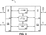
第3図は、ドッキング・ステーション11内のドッキング・チップ130の一実施形態を示す。ドッキング・チップ130はインタフェース回路を備え、このインタフェース回路は、ノート型コンピュータ10とドッキング・ステーション11の間の非事前条件付け(「静止」)ドッキングを容易にするために使用される。前述のように、従来技術の静止ドッキング・システムはインタフェース回路をドッキング・ステーション11ではなくノート型コンピュータ10内に配置していた。
ドッキング・チップは、チップの周縁に4つの入出力(I/O)リング370〜373を含む。これらの入出力リング370〜373は、ドッキング・チップ130に結合される入出力信号線とのインタフェースをとるバッファ・パッドを含む。他の実施形態では、入出力リング370〜373は、3.3V信号および5V信号とのインタフェースをとる分離論理も含む。入出力リング370〜373は走査チェーンなどの試験論理を含むこともできる。入出力バッファ、分離論理、走査チェーンの設計は、当技術分野でよく知られており、したがって、これについて詳しくは論じない。
ノート型コンピュータ入出力リング370は、コネクタ12を介してノート型コンピュータ10に結合されるPCIバス信号とのインタフェースをとることに責任を負う。ノート型コンピュータ制御入出力リング371は、制御信号をコネクタ12を介してノート型コンピュータ10と相互接続する。ドッキング・ステーション入出力リング372はドッキング・ステーション・バス32とのインタフェースをとり、ドッキング・ステーション・バス32は一実施形態ではPCIバスを備える。ドッキング・ステーション制御入出力リング373はドッキング・ステーション制御信号とのインタフェースをとる。
バス制御回路310は、ドッキング・ステーションとノート型コンピュータ・バスを相互接続するブリッジとして働く。一実施形態では、ドッキング・ステーション・バス32とノート型コンピュータ・バス35は共にPCIバスである。したがって、バス制御回路310はPCIバス間ブリッジとして動作し、ノート型コンピュータ10の一次PCIバス35とドッキング・ステーション11の二次PCIバス32を相互接続する。一次PCIバス35または二次PCIバス32上で行われる各トランザクションは、バス制御回路310によって他方のバス上にミラーリングされる。
さらに、他の実施形態では、ドッキング・チップ130が一次PCIバス35と二次ISAバスを相互接続することができる。このような場合、バス制御回路310はPCI−ISA間トランザクションを実行するのに必要なすべての論理も含む。
PCIアービタ論理320は追加のPCI間ブリッジ機能またはPCI・ISA間ブリッジ機能を実行する。一実施形態では、アービタ320は4つのPCI要求/許可対を処理し、ドッキング・ステーションPCIバス32に結合された4つの異なるPCI装置をサポートする。
ドッキング制御回路330は、ドッキング・ステーション11とノート型コンピュータ10を相互接続するためにすべてのドッキング・シーケンス、ドッキング解除シーケンス、中断/再開シーケンスを制御することに責任を負う。これらのシーケンスについては以下で第5図および第6図を参照して詳しく説明する。
第4a図は、ドッキング・ステーション電源150の第1の実施形態を示す。第4a図に示した実施形態は第1のタイプの実施形態であり、ドッキング・ステーション電力モードがノート型コンピュータ電力モードから独立している。信号NBPWROK402(第1図のNB192)は、ノート型コンピュータ電源がイネーブルされていることをドッキング・チップ130に示す。NBPWROK信号402はNBPWRGD信号401(第1図のNBPWRGD194)から生成され、NBPWRGD信号401は、ノート型コンピュータ電源が有効であるときにノート型コンピュータ電源160によって駆動される。NBPWROK信号402は、NBPWRGD信号401をバッファ425を介してオープン・ドレーン信号に変換することによって生成される。次いで、この信号はプルアップ抵抗器428を介してバッテリ電圧VBAT411にプルアップされる。したがって、ノート型コンピュータがドッキングされノート型コンピュータ電源がオフになると、NBPWROK信号402はバッテリの電圧レベルVBAT411にプルされる。
AC電力信号424はドッキング・ステーション電源回路450に結合される。次いで、この信号は5V線形電源420に結合される。5V線形電源420を使用してドッキング・ステーション電力良好信号DSPWG404が生成される。この信号は、ドッキング・ステーションの電力が許容公差(第1図のDS191)内であることをドッキング・チップ130に示す。5V電源420は、ドッキング・ステーション構成要素用のメイン5V電源DSVCC_5V 405(第1図のDSVCC189)を生成するときにも使用される。ドッキング・ステーションはDC/DC変換器421も有し、DC/DC変換器421はQバッファ用のバイアス電圧(第1図のQVCC188)を生成するために使用される。5Vバイアス電圧406と3.3Vバイアス電圧407は共に、5Vノート型コンピュータまたは3.3Vノート型コンピュータをサポートするために生成される。
ドッキング・ステーション電源回路450はそれ自体の小型バッテリ423も含み、このバッテリは、ドッキング・ステーション制御回路330に電力を供給するために使用されるバッテリ電圧VBAT411を生成する。ドッキング・ステーションがそのメイン電源DSVCC_5Vを失ったときに、ドッキング・ステーション制御回路330が引き続き動作できるようにこの小型バッテリが使用される。
ノート型コンピュータをドッキング・ステーション内にドッキングしたときにノート型コンピュータ・バッテリを充電するバッテリ充電信号BAT_CH409(第1図のBAT_CH190)を生成するために充電器422が使用される。一実施形態では、スマート・バッテリが使用され、充電器422はこのスマート・バッテリにもSMBUS408を供給する。
電源回路450は、Qバッファ121用のイネーブル信号QDEN#403(第1図のQDEN#193)を生成するときにも使用される。Qバッファ・イネーブル信号403は、5V電源420のDSPWG電圧をインバータ426を介して反転することによって生成される。
第4b図は、ドッキング・ステーション電源回路150の実施形態を示す。この実施形態では、ドッキング・ステーションが第2のタイプのドッキング・ステーションであり、すなわち、ノート型コンピュータとドッキング・ステーションが同時に同じ電力モードになる。
ノート型コンピュータ電力良好NBPWRGD信号412を使用してノート型コンピュータ電力OK信号NBPWROK413が生成される。NBPWRGD信号412はスイッチに対するイネーブル信号としても使用され、メイン・バッテリ436の出力を5V線形電源434に結合する。
第4b図に示した実施形態では、メイン・バッテリ436が、5V線形電源434に与えられる電圧を供給する。次いで、5V線形電源434の出力が電力良好論理435に供給され、これによって5V信号が有効であることが保証される。電力良好論理435はドッキング・ステーション電力良好信号DSPWG418を生成し、この信号はQバッファ・イネーブル信号QDEN#419を生成するときに使用される。次いで、電力良好論理435からの5V信号がDC/DC変換器に供給され、DC/DC変換器は5Vバイアス電圧414および3Vバイアス電圧415を生成する。
第4a図の電源回路と同様に、第4b図の実施形態は小型バッテリ433とバッテリ充電器432を含む。
第4b図の電源回路では、ドッキング・ステーションがそれ自体のメイン・バッテリ電源436を有する必要があることに留意されたい。代替実施形態として、ノート型コンピュータ電源160からメイン電源が得られるように第4b図の電源回路を実装することができる。
この実施形態では、メイン電源がノート型コンピュータから得られ、電源回路から(点線で分離された)供給回路430が除去される。DC/DC変換器431への5V入力は、電力良好回路435からは得られず、その代わりにノート型コンピュータ電源160から得られる。NBPWRGD信号412は、DSPWG信号418とQDEN#信号419の両方を生成するために使用される。この実施形態の場合、充電器432は任意選択であり、充電回路を備えることができ、この充電回路は、タバコ用ライターや補助DC電源などの電源に差し込むことができる。
本発明の範囲から逸脱せずに前述のドッキング電源150の特定の実施形態を他の周知の電源設計で置き換えられることを理解されたい。
ノート型コンピュータは一般に、バッテリなどの携帯電源によって動作するので、消費電力は、ノート型コンピュータを設計する際に考慮すべき重要なパラメータである。前述のように、ノート型コンピュータとドッキング・ステーションは、コンピュータがアイドル状態であるときに消費される電力量を最小限に抑えるように構成された電力節約モードを使用する。これらの電力節約モード同士の間のインタフェースと、ドッキング・シーケンスおよびドッキング解除シーケンスを制御するインタフェースは、第3図のドッキング制御回路330内に位置する。
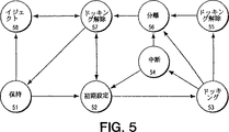
一実施形態では、ドッキング制御回路330は、電力節約イベントおよびドッキング/ドッキング解除イベントを処理するドッキング状態論理を実装した回路を含む。第5図は、ドッキング制御回路330に関する状態図の一実施形態を示す。通常の論理回路を使用してこの状態マシンを実装することができる。
ドッキング解除状態57は、ノート型コンピュータがドッキング・ステーションにドッキングされていないことを示す。また、電源がノート型コンピュータ電源から独立するような、ドッキング・ステーションが第1のタイプのドッキング・ステーションである場合、ドッキング解除状態57は、ノート型コンピュータまたはドッキング・ステーションの電源がオフであることを示す。ノート型コンピュータがドッキング・ステーションに挿入されたことが、CD1#信号とCD2#信号の両方のアサートによって示されると、ドッキング状態マシンはドッキング解除状態57から開始する。
他の状態からドッキング解除状態57に入ったときにはいつでも、回路330は二次(ドッキング・ステーション)PCIバスから一次(ノート型コンピュータ)PCIバスを分離する。回路330は、QPCIEN#信号183をアサート解除することによって第1図のPCI Qバッファ121をオフにし、ドッキング・ステーションPCIバス上で二次PCIバス・リセット信号sRST#をアサートする。
一実施形態では、CD1#信号またはCD2#信号がアサート解除されたときにはいつでも、回路330がドッキング解除状態57に入る。これは、ノート型コンピュータのドッキング・ステーションからの予期しないイジェクトとみなされる。この場合、ドッキング・ステーション・チップ130は、第7図を参照して詳しく説明するように、PCIトランザクションに影響を与えずにPCIバスを分離する。
さらに、本発明の一実施形態では、ノート型コンピュータをドッキング・ステーションから取り外すにはノート型コンピュータをロック解除またはイジェクトしなければならない。したがって、この実施形態の場合、状態マシンがドッキング解除状態57になったときにそのことがロック解除機構またはイジェクト機構に知らされ、それによってノート型コンピュータをロック解除またはイジェクトすることができる。
回路330は、中断していたノート型コンピュータが第2の(従属電源)タイプのドッキング・ステーション内に取り付けられるか、あるいは中断していたノート型コンピュータが、電力を供給されている第1の(独立電源)タイプのドッキング・ステーション内に取り付けられたと判定した場合、保持状態51に移行する。電力を供給されているノート型コンピュータが、電力を供給されている第1のタイプのドッキング・ステーションに挿入された場合、回路330はドッキング解除状態57から初期設定状態52に移行する。
保持状態51は、中断していたノート型コンピュータに、再開信号をパルスすることによりノート型コンピュータ内の電力を再開することによって初期設定状態に入る準備をさせる。NBPWROK信号がアサートされることによって、ノート型コンピュータの電力が良好であることが判定された後、状態マシンは初期設定状態に移行する。
一実施形態では、ドッキング・ステーションはオープン要求ボタンを含み、このボタンは、システムのユーザからアクセスすることができ、押されるとOPENREQ信号をアサートする。この信号は、状態マシンに経路指定され、ユーザがノート型コンピュータを取り外す必要があることを示す。状態マシンが保持状態51である間にOPENREQ信号がアサートされた場合、回路330はイジェクト状態58に移行し、ノート型コンピュータをドッキング解除する。
ドッキング・ステーションとノート型コンピュータの両方の電源がオンになっており、かつノート型コンピュータがドッキングされたときにはいつでも、初期設定状態52に入ることができる。初期設定状態52は、ドッキングされたノート型コンピュータに、静止ドッキング・シーケンスを実行することによってドッキング状態53に入る準備をさせる。静止ドッキング・シーケンスは、第1図のドッキング電源論理150への信号をアサートすることによってバイアス電圧をオンにするステップから始まる。次いで、PCIクロックQバッファ121がイネーブルされる。その後、回路330は、ノート型コンピュータにPCIバスの制御を要求し、制御が与えられた後、QPCIEN#183信号をアサートすることによってPCI Qバッファ120をイネーブルする。
ノート型コンピュータがドッキング・ステーションに挿入された後、ソフトウェア・ルーチンは、電気的に消去可能なプログラム可能読取り専用メモリ(EEPROM)などのメモリ内に記憶されているドッキング・ステーション識別番号を検査する。この特定のドッキング・ステーションにはまだノート型コンピュータが結合されていないと判定された場合、ソフトウェアはドッキング・ステーションのハードウェア装置をポーリングし、次いで必要なソフトウェア・ドライバをロードする。ドライバが得られない場合、ソフトウェアはプロンプトを出してユーザにドライバを求める。次いで、ノート型コンピュータは、次にこのドッキング・ステーションに挿入されたときにすべての必要なドライバを含むように、ドッキング・ステーションの識別番号を記憶する。
ノート型コンピュータが初期設定され、ノート型コンピュータ電源がオンになった後、初期設定状態からドッキング状態53に入る。次いで、回路330は中断状態54、分離状態56、またはドッキング解除状態55に入る。
ノート型コンピュータが1つの中断モードに入った場合、回路330は中断状態54に移行する。ノート型コンピュータまたはドッキング・ステーションがオフになった場合、回路330は分離状態56に入る。ドッキング解除シーケンスが必要であることをソフトウェア・ルーチンが示している場合、ドッキング状態マシンはドッキング解除状態55に入る。
中断状態54は、ドッキング回路330が入ることのできる2つの中断状態、すなわち電源オン中断と電源オフ中断の一方を表す。ドッキング状態マシンの電源オン中断状態は、ノート型コンピュータの電源オン中断モードと共に使用される。電源オフ中断状態は、前述の3つのノート型コンピュータ中断モード、たとえば電源オン中断、DRAM保存後中断、ディスク保存後中断のうちの1つと共に使用される。
ノート型コンピュータが電源オン・バージョンの中断モードに入っても、ドッキング・ステーションはドッキング状態53のままである。電源オフ中断バージョンの中断状態54に入ると、ドッキング・ステーションの電源がオフになる。システムは、ドッキング・ステーションの電源をオフにする前に、ドッキング・ステーション装置のコンテキストを保存する。ドッキング状態マシンは第1図のPCI Qバッファ120をディスエーブルし、Qバッファ・バイアス電圧QVCC188をオフにし、ノート型コンピュータが再開するのを待つ。
ノート型コンピュータをドッキング・ステーションからドッキング解除するときにはドッキング解除状態55に入る。ドッキング解除状態55に入る前に、ソフトウェア・ルーチンは、ドッキング・ステーション資源を使用しているアプリケーションをシャットダウンするようオペレーティング・システムに通知しておくべきである。オペレーティング・システムがこのプロセスを完了した後、ソフトウェア・ルーチンは、ドッキング解除シーケンスが必要であることを回路330に示す。次いで、分離状態56に入る。回路330は、Qバッファ120をディスエーブルするQPCIEN#183をアサート解除する。これにより、第7図を参照して詳しく説明するように、現在のトランザクションを妨害せずにPCIバスが分離される。
次いで、回路330はOPEN信号を生成し、イジェクト機構またはロック解除機構に、ノート型コンピュータをドッキング・コネクタからイジェクトまたはロック解除するよう指示する。パルスが生成された後、回路330は分離状態56に移行する。
電源オフ・ノート型コンピュータが電源オン・ドッキング・ステーションに接続されたときにはいつでも、イジェクト状態58が使用される。システムのユーザはイジェクト・ボタンを押し、それによって回路330にOPENREQ信号をパルスする。次いで、回路330がイジェクト状態58に入り、OPENパルスが生成され、ノート型コンピュータがドッキング・ステーションからイジェクトまたはロック解除される。
特定の電力モード、信号名、回路構成要素を参照して第5図の回路330について説明したが、本発明の範囲から逸脱せずに他の周知のモード、信号、回路で置き換えられることを理解されたい。たとえば、ノート型コンピュータを所定の位置に保持するイジェクト機構またはロッキング機構のないドッキング・ステーションではOPENパルスを生成する必要はない。
一実施形態では、第5図に示した状態マシンは回路330内のプログラマブル・ロジック・アレイ(PLA)として実装される。別法として、状態マシンは、組合せ論理など当業者によく知られている他の形態の回路に実装することができる。
本発明の方法の詳細な説明
第6図は、ノート型コンピュータをドッキング・ステーションにドッキングし、かつドッキング・ステーションからドッキング解除する方法を示す。第6図の方法について、第1図に示した構成要素を参照して説明する。
第1のステップ610は、ノート型コンピュータ10のドッキング・ステーション11内への挿入を示す。適切に接続された場合、コネクタ12内のCD1#信号とCD2#信号の両方がアサートされる。次いで、この方法はステップ612に移る。ノート型コンピュータ11がドッキング・ステーション11内に挿入されていない場合、この方法はステップ632に移行する。この場合、ノート型コンピュータ10は、イジェクトされているか、あるいはドッキング・ステーションに適切に取り付けられていない。システムは、ステップ610で接続が検出されるまでステップ632に留まる。
ステップ612では、ドッキング・ステーション11内にノート型コンピュータが挿入された後、ノート型コンピュータ10の電源がオンになっているかどうかをドッキング・ステーション11が判定しなければならない。第4図のNBPWROK信号402がアサートされると、ノート型コンピュータ10の電源がオンになる。次いで、この方法はステップ614に移行する。NBPWROK信号402がアサート解除されると、ステップ628で、ドッキング・ステーション11は、ノート型コンピュータ10が中断状態であるかどうかを判定する。このことは、SUS#信号186がアサートされることによって示され、SUS#信号186はドッキング・ステーション・コネクタ12を通るように経路指定される。
ノート型コンピュータ10は、中断されている場合、ステップ630で、ドッキング・シーケンスが続行される前にドッキング・ステーション11によって再開される。ドッキング・ステーション11はSRBTN#信号184をアサートすることによってノート型コンピュータ10を再開し、この信号はドッキング・ステーション・コネクタ12を通るように経路指定される。その後、ステップ612が再び実行されるときに、ノート型コンピュータ10の電源がオンであるかどうかを判定すべきである。
ステップ614で、静止ドッキング手順が実行される。静止ドッキング手順については上記で第5図を参照して説明したが、この手順は、バイアス電圧をオンにするステップ、PCIクロックQバッファ121をイネーブルするステップ、PCI Qバッファ120をイネーブルするステップを含む。次いで、ドッキング・チップ130は、ステップ614の静止ドッキング手順が完了したことをシステム・ソフトウェアに示す割込み(第1図のDCKINTR182)を生成する。この特定のドッキング・ステーション11にノート型コンピュータ10を挿入するのが初めてである場合は、DCKINTR182信号に応答して、装置に必要なドライバをドッキング・ステーション11上にロードすることによってコンピュータ・システムが構成される。
この場合、ステップ616によって示したように、ノート型コンピュータ10およびドッキング・ステーション11は動作可能であり電力を供給されている。ステップ618で、ドッキング・チップ130はSUS#信号186の状態を監視し、ノート型コンピュータが中断モードに入るかどうかを検出する。
ノート型コンピュータが中断モードに入ることをSUS#186信号が示していない場合、ステップ636でドッキング・チップ130は、イジェクト要求が示されているかどうかを検査する。イジェクト要求とは、ノート型コンピュータをドッキング・ステーションからドッキング解除することを求めるソフトウェア・ルーチンからの要求であり、これについては上記で詳しく説明した。本発明の一実施形態では、コンピュータ・システムのユーザはドッキング解除ボタンを押してドッキング解除シーケンスを開始することができる。これによってステップ636が実行され、ユーザがドッキング解除ボタンを押したことはOPENREQ信号によって示される。
イジェクトが要求された場合、ステップ634で静止ドッキング解除シーケンスが実行される。前述のように、静止ドッキング解除シーケンスは、ドッキング・ステーション資源を使用するアプリケーションをシャットダウンするステップ、ノート型コンピュータPCIバスをドッキング・ステーションPCIバスから分離するステップ、ノート型コンピュータをドッキング・ステーション・コネクタ12からロック解除またはイジェクトするステップを含む。
ステップ632で、ドッキング・ステーション11はノート型コンピュータが挿入されるのを待つ。
ステップ618に戻り、ノート型コンピュータがイジェクトされずに中断モードに入ると判定された場合、ステップ620が実行される。ステップ620で、ノート型コンピュータ10およびドッキング・ステーション11は中断モードに入る。イジェクトが要求されているか、あるいは再開イベントが検出された場合、ノート型コンピュータ10およびドッキング・ステーション11は中断モードを終了する。再開イベントが検出され、かつイジェクトが要求されていない場合、回路330は静止ドッキング・シーケンスを実行し、ステップ614を介してステップ616に進む(点線で示されている)。
ステップ622によって示したように、ノート型コンピュータ10およびドッキング・ステーション11が中断モードである間にイジェクトが要求されたと判定された場合、ステップ624で、静止ドッキング解除シーケンスが実行される前にノート型コンピュータ10が再開される。ノート型コンピュータ10は、ドッキング・チップ130によりSRBTN#信号184をアサートすることによって再開される。ステップ622でイジェクトが要求されていない場合、ノート型コンピュータ10は、再開されるまで中断モードのままである。
ステップ626でノート型コンピュータ10が再開を完了したかどうかを判定する。ノート型コンピュータが電力を再開すると、NBPWROK信号192がアサートされる。ノート型コンピュータ10が再開した後、ステップ634の静止ドッキング・シーケンスが実行される。
前述のように、静止ドッキング解除シーケンスは、進行しているPCIトランザクションに割り込まずに一次ノート型コンピュータPCIバスを二次ドッキング・ステーションPCIバスから分離するステップを含む。従来技術のドッキング解除方法は、PCIバス上のトランザクションを要求するステップ、トランザクションが許可されるのを待つステップ、次いでトランザクションが行われていないときにPCIバスの分離を可能にするステップを含む。このような方法では、バスは分離されるときにアイドル状態になる。したがって、トランザクションは、分離中の負荷の変化のためにバス上で起こる恐れのある信号の変動の影響を受けない。
これに対して、本発明のドッキング解除方法では、ドッキング・チップ130が分離の前にPCIバス180の制御を要求する必要がない。本発明の方法は、PCI Special Interest Group(SIG)から市販されているPCI Specificationバージョン2.1で指定された所定のPCI信号セットアップ時間よりも前に分離を行うことを可能にする。
第7図のタイミング図は、本発明のドッキング解除信号プロトコルの一実施形態を示す。図の信号はPCIクロック710、PCIバス720、QPCIEN#信号730である。QPCIEN#信号730が第1図のPCI Qバッファ120をイネーブルし、かつディスエーブルすることを想起されたい。Qバッファ120がディスエーブルされると、一次ノート型コンピュータPCIバス180が二次ドッキング・ステーションPCIバスから分離され、ノート型コンピュータ10をドッキング・ステーション11から取り外すことができることを想起されたい。
Qバッファ120がディスエーブルされると、ドッキング・ステーションのPCI装置はもはや一次PCIバスに結合されていないので、一次ノート型コンピュータPCIバスが検出する負荷はずっと小さくなる。したがって、ノート型コンピュータPCIバス上の信号は負荷の変化による電圧の変動を受ける可能性がある。このため、ノート型コンピュータPCIバス上で行われているPCIトランザクションに対する問題が生じる恐れがある。したがって、本発明はPCIクロックの立上りと次のクロックのセットアップ時間の開始点との間にPCI Qバッファ120をディスエーブルする方法を提供する。
本発明のドッキング解除機構は第1図のドッキング制御回路130によって制御される。ドッキング制御回路は、PCIバス上のセットアップ時間よりも前にQPCIEN#信号がアサートされるようにノート型コンピュータとドッキング・ステーションを相互接続する。
第7図を参照すると、PCIクロック710の4つのサイクル700〜703が示されている。PCIプロトコルによれば、すべての信号は、点線で示したPCIクロックの立上りでラッチされる。立上りで正しい信号値がラッチされるように、信号は、次のクロックの立上りまでの時間として定義されるセットアップ時間において安定な値でなければならない。
本発明では、PCIバス720上の信号はセットアップ時間までに安定する。QPCIEN#信号730は点71のPCIクロックの立上りで、あるいはこの立上りよりもわずかに後でアサート解除される。点71と点72の間の陰影の付いた領域は、QPCIEN#信号をアサート解除することのできる有効な遅延時間を示す。この場合、PCI Qバッファ120は、定義済みのPCIセットアップ時間の開始点を示す点73よりも前の、陰影の付いた領域内のある時点でディスエーブルされる。したがって、PCIバス720上の信号はクロック703の立上りまでに安定な値になる。
したがって、ノート型コンピュータをドッキング・ステーションにドッキングし、ドッキング・ステーションからドッキング解除する方法および装置について説明した。本明細書で説明したドッキング・ステーションの実施形態は単一のノート型コンピュータに対処するように設計されているが、このドッキング・ステーションが複数のノート型コンピュータにも対処できることを理解されたい。この代替実施形態の場合、ノート型コンピュータとドッキング・ステーションの間のインタフェースは、本発明によれば、第1図のドッキング・チップ130など単一のドッキング・チップ内に存在することも、あるいは複数のドッキング・チップ内に存在することもできる。
本発明の方法および装置について現在好ましい形態に関して説明したが、当業者には、本発明の方法が前述の現在好ましい形態に限らないことが認識されよう。本発明の方法および装置は、添付の特許請求の範囲の趣旨および範囲内で修正および変更することができる。したがって、本明細書は、本発明を制限するものではなく例示するものとみなすべきである。 Cross-reference of related applications
This application is related to United States Patent Application No. ______ entitled “METHOD AND APPARATUS FOR DOCKING AND UNDOCKING A NOTEBOOK COMPUTER” filed on the same date as this application.
Field of Invention
The present invention relates to the field of computer systems. In particular, the present invention relates to docking and undocking a notebook computer to and from a docking station.
Background of the Invention
Currently, notebook (portable) computers incorporate many features that were previously only available on desktop personal computers. By using a docking station connected to a notebook computer, a user can access various services that are usually available only on a desktop computer. Thus, when a notebook computer is connected to or attached to a docking station, the resulting system is similar to a desktop computer.
A notebook computer is typically connected to a docking station by using a socket type connection. That is, the notebook computer is inserted into the docking station, and upon such insertion, it is connected to the docking station by using a mating connector. Upon disengaging the notebook computer from the docking station, the notebook computer is simply removed from the docking station.
One important problem with prior art methods of inserting and removing a notebook computer from a docking station is that the insertion or removal process cannot be performed without manual intervention by the user.
Accordingly, other conventional docking and undocking methods use circuitry that allows a user to insert and remove a notebook computer from the docking station without prior conditioning. Therefore, even when an application program is executed on the notebook computer, the notebook computer can be inserted into the docking station or removed from the docking station without interrupting the application program.
Prior art systems use an interface that includes a docking chip. This interface exists in a notebook computer that handles the insertion and removal algorithms. While this prior art system is advantageous in that it allows docking and undocking without preconditioning, it has the disadvantage of increasing the complexity of the notebook computer due to the increased number of circuit components. The more circuit components included in a notebook computer, the more battery consumption, the higher the manufacturing cost of the notebook computer, and the larger the notebook computer.
Summary of the Invention
A method and apparatus for docking a notebook computer to a docking station without preconditioning is described. The apparatus includes interface circuitry located within the docking station for interconnecting the notebook computer and the docking station. This interface detects when a notebook computer is inserted into the docking station and correspondingly switches the common system bus between the notebook computer and the docking station. Enable. The interface also generates events that allow software to configure notebook computers and docking stations without user prior intervention.
[Brief description of the drawings]
The present invention will become more fully understood from the detailed description given below and the accompanying drawings of various embodiments of the invention. However, this description and drawings are not to be construed as limiting the invention to the specific embodiments, but are for explanation and understanding only.
FIG. 1 is a block diagram of the notebook computer and docking station of the present invention.
FIG. 2 is a view showing an embodiment of the docking station connector of the present invention.
FIG. 3 illustrates a docking interface chip according to an embodiment of the present invention.
FIG. 4a is a diagram showing a first embodiment of a docking station power supply according to the present invention.
FIG. 4b shows a second embodiment of the docking station power supply according to the present invention.
FIG. 5 is a state diagram of a docking state machine according to one embodiment of the present invention.
FIG. 6 is a flowchart illustrating a method for handling docking and undocking of a notebook computer.
FIG. 7 is a timing diagram of signals asserted in one embodiment of the present invention.
Detailed Description of the Invention
A method and apparatus for docking and undocking a notebook computer is described. In the following detailed description of the present invention, numerous specific details are set forth such as specific bus protocols, voltages, event names, interrupt names, etc., in order to provide a thorough understanding of the present invention. However, it will be apparent to one skilled in the art that the present invention may be practiced without these specific details. In other instances, well-known structures and devices are shown in block diagram form, rather than in detail, in order to avoid obscuring the present invention.
Summary of the Invention
The present invention provides a non-preconditioning automatic insertion / removal protocol between a notebook computer and a docking station that does not require user intervention. Furthermore, the present invention is advantageous in that the docking interface is located in the docking station rather than in the notebook computer.
When the notebook computer is inserted into the docking station, it is coupled to the docking station via a connector. The connector includes pins that couple common signal lines between the notebook computer and the docking station. For example, a connector is used to connect a common system bus between a notebook computer and a docking station.
This common system bus is also coupled to a switch. This switch is controlled by an interface circuit in the docking station. When the interface circuit detects that a notebook computer has been inserted into the docking station, the switch is closed and the notebook computer's common system bus is coupled to the docking station. However, because a transaction is taking place on the common system bus, the switch will not close until the interface circuit determines that it is safe to close the switch without interrupting the transaction. Therefore, the interface circuit requests control of the common system bus and then closes the switch after control is given to the interface circuit.
In one embodiment of the invention, the interface circuit generates a docking event after the switch is closed. This event is detected by a software routine that automatically configures the notebook computer and docking station without any prior user intervention. For example, the software routine can load the device drivers needed for the device into a docking station coupled to a common system bus.
When the notebook computer is inserted into the docking station, it may be in a suspended mode or in a normal mode. In one embodiment of the invention, the interface circuit checks the mode of the notebook computer upon insertion. If the notebook computer is in suspend mode, the interface circuit causes the notebook computer to resume in normal mode before closing the switch and generating a docking event.
After the notebook computer is docked at the docking station, it can enter suspend mode. In one embodiment, the interface circuit detects that the notebook computer enters suspend mode, thereby also placing the docking station in suspend mode.
The interface circuit also detects when the notebook computer is removed from the docking station. The interface circuit detects the removal by detecting a physical removal from the docking station of the notebook computer or by receiving an eject request from a system user or software routine. In response to this removal, the interface circuit first generates an undock event, which causes the software to prepare the computer system for removal of the notebook computer. The interface circuit then opens a switch to isolate the common system bus.
When an eject request is detected by the interface circuit, the notebook computer may be in a suspended mode or in a normal mode. In one embodiment, if the notebook computer is in suspend mode when an eject request is detected, the interface circuit causes the notebook computer to resume in normal mode before generating an undock event and opening the switch.
When the software routine detects an undocking event, it configures the notebook computer and docking station so that the notebook computer can be removed. Recall that an event, such as an undocking event, is generated by the interface circuit to allow software routines to configure the notebook computer and docking station upon insertion or removal. Such an event is automatically generated by an interface circuit in the docking station. Thus, no manual intervention is required before the user initiates docking or undocking.
Since a transaction is taking place on the common system bus when a removal is detected, the interface circuit opens the switch when a change in common system bus capacitance does not affect the transaction. The interface circuit opens the switch between the rising edge of the system bus clock and the setup time of the next system bus clock. Thus, if the signal on the common system bus fluctuates because the switch is open, the signal will stabilize by the next clock setup time.
The present invention automatically detects notebook computer and docking station conditions or states, automatically controls notebook computer or docking station power, generates and inserts events related to system software interactions Automatically isolate and enable interconnect signals during the process or removal process, or while the notebook computer is fully installed, prevent the interconnect signals from colliding, and locate and allocate resources.
Note that the software routines referred to in the present invention control the operation of the hardware in the computer system and can be implemented in various programming languages. For example, such software routines can include a basic input / output system (BIOS) written in assembly language. This software can be fully or partially implemented as firmware, runtime library routines, or operating system procedures.
Detailed description of the apparatus of the present invention
FIG. 1 is a block diagram of one embodiment of the system of the present invention. As can be seen with reference to FIG. 1, the system includes a docking station 11 and a notebook computer 10, each of which is shown separated by a dotted line. A connector 12 is positioned between the notebook computer 10 and the docking station 11 to facilitate electrical connection of signals between the two. The notebook computer 10 is said to be “attached” within the docking station when properly coupled to the mating connector 12 of the docking station 11.
In the illustrated embodiment, the notebook computer 10 includes a
The notebook computer 10 can also include an input / output controller (not shown), which is coupled to the
PCI
When enabled, Q buffers 120 and 121 buffer common signals between notebook computer 10 and docking station 11. Q buffers 120 and 121 also separate each common signal of notebook computer 10 and docking station 11 when disabled. In one embodiment, Q buffers 120 and 121 act as switches, and when disabled, the signal coupled to Q buffers 120-121 is tri-stated, thereby removing notebook computer 10 from docking station 11. be able to.
During the docking sequence,
In one embodiment, the PCI clock on
In one embodiment, the docking station 11 has a
Suspend mode is a power saving state that causes the notebook computer 10 or docking station 11 to consume significantly less power when the system is not in use. There are several interruption modes that can be implemented in the docking station 11 or the notebook computer 10. For example, the “power on interrupt” mode disables all clocks in the system except the real time clock (RTC). The only power consumed in this state is the leakage power in the system. When resuming the system from the power-on suspend mode, the clock is simply resumed.
The “suspend after DRAM save” mode turns off power to all devices except power management logic, memory refresh logic, and frame buffer refresh logic. Before calling the suspend mode after saving the DRAM, the context of each device in the system must be saved in the DRAM. When the system is resumed from the suspend mode after saving the DRAM, all devices must be reset and the context of each device must be regenerated.
“Suspend after disk save” mode saves the entire context of the computer system in non-volatile memory (eg, a hard disk) and turns off power to the entire system. When exiting suspend mode after saving the disk, all devices in the computer system must be repowered, reset, and replayed the context stored on the hard disk.
As described above, in one embodiment, the notebook computer 10 and the docking station 11 can invoke independent power modes. Thus, the notebook computer 10 or docking station 11 can enter one of the interrupt modes at any time.
In other embodiments, the docking station 11 is a portable docking station, and the docking
In the case of a desktop docking station, the docking
In one embodiment, the docking station 11 can be docked to the notebook computer 10 operating at 3.3V or 5V. In this embodiment, the docking
The docking connector 12 connects the notebook computer 10 and the docking station 11. The docking connector 12 includes a number of pins that are used to communicate between the notebook computer 10 and the docking station 11. The signal lines in the docking station 11 shown in FIG. 1 will be discussed in detail below with reference to the docking connector 12, the
FIG. 2 shows one embodiment of the docking connector 12, where the notebook computer side of the docking connector 12 comprises a female connector and the docking station side of the docking connector 12 comprises a male connector. . It should be understood that any known connector type can be used to implement the connector 12 without departing from the scope of the present invention. Further, the notebook computer side of the docking connector 12 may include pins, and the docking station side of the docking connector may include a socket.
This detection is facilitated by the connector detection pins being positioned at the respective ends of the docking connector 12. When both the
Note that in one embodiment, the
The longer pins 21b-25b indicate other signals that are coupled between the notebook computer 10 and the docking station 11. The GND connections 25 a-b represent the ground plane used by both the notebook computer 10 and the docking station 11. In one embodiment, the
The NB_SW signal lines 24 a-b connect the 5 V power signal from the notebook computer 10 to the docking station 11. The 5V power signal is then routed to the
Battery charging (BAT_CH) connections 22 a-22 b are battery charging signal lines that are sent from the docking
The
For embodiments where the notebook computer 10 includes an ISA bus, ISA signals are similarly routed through the connector 12. The ISA support signal includes a predefined ISA IRQ.
In one embodiment, six docking management signals are routed through connector 12. These signals include NBPWRGD, a notebook computer “good power” signal. This signal indicates that the 5V power in the notebook computer is within acceptable tolerances. The SUS # signal indicates that the notebook computer is suspended and the 5V power is within acceptable tolerances at the docking station. The QDEN # signal and the QPCIEN # signal are used to enable the Q buffers 120 and 121 on the notebook computer 10. DCKINTR # is a docking station interrupt and is used to signal a docking event, and the SRBTN # signal is generated by the
The docking station connector 12 also includes a number of pins for passive wired signals that are used to facilitate communication between the input device and the output device. For example, LPT port signals and COM port signals are routed through connector 12. In addition, keyboard signals, mouse signals, floppy drive signals, cathode ray tube (CRT) signals, telephone signals, microphone signals, and speaker signals are routed through connector 12 as needed. It should be understood that the docking connector 12 can be implemented by arbitrarily combining a greater or lesser number of signals than described herein without departing from the scope of the present invention.
FIG. 3 shows an embodiment of the
The docking chip includes four input / output (I / O) rings 370-373 at the periphery of the chip. These input / output rings 370-373 include buffer pads that interface with input / output signal lines coupled to
The notebook computer input /
The bus control circuit 310 serves as a bridge that interconnects the docking station and the notebook computer bus. In one embodiment,
Further, in other embodiments, the
The
The
FIG. 4 a shows a first embodiment of the docking
The docking station power circuit 450 also includes its own
A
The power supply circuit 450 is also used when generating the enable signal QDEN # 403 (
FIG. 4 b shows an embodiment of the docking station
The notebook computer power OK signal
In the embodiment shown in FIG. 4b, the
Similar to the power circuit of FIG. 4 a, the embodiment of FIG. 4 b includes a small battery 433 and a
Note that in the power circuit of FIG. 4b, the docking station needs to have its own main
In this embodiment, the main power supply is obtained from a notebook computer and the supply circuit 430 (separated by a dotted line) is removed from the power supply circuit. The 5V input to the DC /
It should be understood that certain embodiments of the
Since notebook computers generally operate with a portable power source such as a battery, power consumption is an important parameter to consider when designing a notebook computer. As mentioned above, notebook computers and docking stations use a power saving mode that is configured to minimize the amount of power consumed when the computer is idle. The interface between these power saving modes and the interface for controlling the docking sequence and the undocking sequence are located in the
In one embodiment, the
The undocked
Whenever the
In one embodiment,
Furthermore, in one embodiment of the present invention, the notebook computer must be unlocked or ejected to be removed from the docking station. Thus, in this embodiment, when the state machine enters the undocking
The
The holding
In one embodiment, the docking station includes an open request button that can be accessed by a user of the system and asserts the OPENREQ signal when pressed. This signal is routed to the state machine and indicates that the user needs to remove the notebook computer. If the OPENREQ signal is asserted while the state machine is in
The
After the notebook computer is inserted into the docking station, the software routine checks the docking station identification number stored in a memory, such as an electrically erasable programmable read only memory (EEPROM). If it is determined that a notebook computer is not yet coupled to this particular docking station, the software polls the docking station's hardware device and then loads the necessary software drivers. If no driver is available, the software prompts the user for a driver. The notebook computer then stores the docking station identification number to include all necessary drivers the next time it is inserted into the docking station.
After the notebook computer is initialized and the notebook computer is turned on, the docking state 53 is entered from the initial setting state. The
If the notebook computer enters one suspend mode,
The interrupt
The docking station remains in the docked state 53 when the notebook computer enters the power-on version interrupt mode. Upon entering the suspended
Undocking
The
Although the
In one embodiment, the state machine shown in FIG. 5 is implemented as a programmable logic array (PLA) in
Detailed description of the method of the invention
FIG. 6 illustrates a method for docking and undocking a notebook computer from a docking station. The method of FIG. 6 will be described with reference to the components shown in FIG.
The first step 610 shows the insertion of the notebook computer 10 into the docking station 11. When properly connected, both the CD1 # and CD2 # signals in connector 12 are asserted. The method then moves to step 612. If the notebook computer 11 is not inserted into the docking station 11, the method moves to step 632. In this case, the notebook computer 10 is either ejected or not properly attached to the docking station. The system remains at step 632 until a connection is detected at step 610.
In
If interrupted, the notebook computer 10 is resumed by the docking station 11 at
At
In this case, as indicated by
If the SUS # 186 signal does not indicate that the notebook computer will enter suspend mode, then at
If ejection is requested, a static docking release sequence is executed at
In step 632, the docking station 11 waits for a notebook computer to be inserted.
Returning to step 618, if it is determined that the notebook computer has entered the suspend mode without being ejected, step 620 is executed. At step 620, notebook computer 10 and docking station 11 enter suspend mode. If an eject is requested or a resume event is detected, the notebook computer 10 and the docking station 11 exit the suspend mode. If a resume event is detected and no eject is requested,
If it is determined that an eject was requested while the notebook computer 10 and the docking station 11 were in suspend mode, as indicated by
In
As described above, the static undocking sequence includes separating the primary notebook computer PCI bus from the secondary docking station PCI bus without interrupting ongoing PCI transactions. Prior art undocking methods include the steps of requesting a transaction on the PCI bus, waiting for the transaction to be granted, and then allowing the PCI bus to be detached when no transaction is taking place. In such a method, the bus is idle when it is separated. Thus, the transaction is not affected by signal variations that may occur on the bus due to load changes during isolation.
On the other hand, in the docking release method of the present invention, the
The timing diagram of FIG. 7 illustrates one embodiment of the undock signal protocol of the present invention. The illustrated signals are a
When the
The docking release mechanism of the present invention is controlled by the
Referring to FIG. 7, four cycles 700-703 of the
In the present invention, the signal on the PCI bus 720 is stable by the setup time. The
Accordingly, a method and apparatus have been described for docking a notebook computer to a docking station and undocking from the docking station. Although the docking station embodiments described herein are designed to accommodate a single notebook computer, it should be understood that the docking station can also accommodate multiple notebook computers. In this alternative embodiment, the interface between the notebook computer and the docking station may be present in a single docking chip, such as the
Although the method and apparatus of the present invention have been described with respect to presently preferred forms, those skilled in the art will recognize that the method of the present invention is not limited to the presently preferred forms described above. The method and apparatus of the present invention can be modified and changed within the spirit and scope of the appended claims. Accordingly, the specification is to be regarded as illustrative rather than limiting on the invention.
Claims (13)
前記ドッキング・ステーション内に位置し、前記ノート型コンピュータが前記ドッキング・ステーション内に挿入されたときにそのことを検出し、それに対応して、前記ノート型コンピュータと前記ドッキング・ステーションの間に共通システム・バスが結合されるようにスイッチをイネーブルし、ソフトウェア・ルーチンがユーザの介入なしにノート型コンピュータおよびドッキング・ステーションを構成することを可能にするイベントを生成するドッキング・ステーション回路を備え、
このドッキング・ステーション回路を、さらに、イジェクト要求イベントを検出し、それに対応して、前記共通システム・バス上で行われているトランザクションが影響を受けないように前記ノート型コンピュータと前記ドッキング・ステーションの間で前記共通システム・バスを分離し、その際、前記共通システム・バスのシステム・バス・クロック・サイクルの立上りから次のシステム・バス・クロック・サイクルのセットアップ時間の開始までの間で前記スイッチをディスエーブルすることによって前記共通システム・バスを分離するよう構成したことを特徴とするインタフェース。An interface for stationary docking to a notebook computer docking station without preconditioning,
A system located within the docking station that detects when the notebook computer is inserted into the docking station and correspondingly a common system between the notebook computer and the docking station Comprises a docking station circuit that enables a switch to couple the bus and generates an event that allows a software routine to configure the notebook computer and docking station without user intervention;
The docking station circuitry further detects an eject request event and correspondingly, the common system bus on a performed by that transaction the notebook computer so as not to be influenced by the docking station Separating the common system bus between the switches of the common system bus from the rise of the system bus clock cycle to the start of the setup time of the next system bus clock cycle. An interface configured to isolate the common system bus by disabling the interface.
前記スイッチをイネーブルする前に、前記ドッキング・ステーション回路は前記ノート型コンピュータの電力状態を決定し、それが中断状態であった場合に、前記ドッキング・ステーション回路は、動作を再開するよう前記ノート型コンピュータに要求することを特徴とするインタフェース。Prior to enabling the switch, the docking station circuit determines the power state of the notebook computer, and if it is suspended, the docking station circuit causes the notebook computer to resume operation. An interface characterized by requiring a computer.
前記ノート型コンピュータが電源オンされているときに、前記ドッキング・ステーション回路は前記共通システム・バスを制御する要求を生成し、該共通システム・バスの制御の下で前記スイッチをイネーブルすることを特徴とするインタフェース。When the notebook computer is powered on, the docking station circuit generates a request to control the common system bus and enables the switch under control of the common system bus. Interface.
(B)ドッキング・ステーションと
を有し、ドッキング・ステーションが
(i)ノート型コンピュータがドッキング・コネクタに挿入されたときにノート型コンピュータとドッキング・ステーションの間で複数の共通信号を結合し、前記複数の共通信号のうちの、共通システム・バスを介する1組の共通システム・バス信号がさらにスイッチに結合されるドッキング・コネクタと、
(ii)ノート型コンピュータがドッキング・コネクタに挿入されたことを検出し、それに対応して、
前記共通システム・バス信号が前記ノート型コンピュータとドッキング・ステーションの間に結合されるように前記スイッチをイネーブルし、
ソフトウェア・ルーチンがユーザの介入なしにノート型コンピュータおよびドッキング・ステーションを構成することを可能にするイベントを生成するインタフェース回路とを有し、
(iii)前記インタフェース回路を、さらに、イジェクト要求イベントを検出し、それに対応して、前記共通システム・バスのシステム・バス・クロック・サイクルの立上りから次のシステム・バス・クロック・サイクルのセットアップ時間の開始までの間で前記スイッチをディスエーブルすることによって、前記共通システム上で行われているトランザクションが影響を受けないように、前記ノート型コンピュータと前記ドッキング・ステーションの間で前記共通システム・バス信号を分離するよう構成したことを特徴とするコンピュータ・システム。(A) a notebook computer;
(B) and a docking station, and coupling a plurality of common signals between the notebook computer and docking station when the docking station is (i) notebook computer is inserted into the docking connector, wherein and docking connector of the plurality of common signal, a set of common system bus signals via a common system bus is further coupled to a switch,
(Ii) detect that a notebook computer has been inserted into the docking connector and in response,
Enabling the switch so that the common system bus signal is coupled between the notebook computer and a docking station;
An interface circuit for generating an event that allows a software routine to configure a notebook computer and a docking station without user intervention;
The (iii) wherein the interface circuit further detects an eject request event and correspondingly, the common system bus system bus clock system rising from the next cycle bus clock cycle setup time of The common system bus between the notebook computer and the docking station so that transactions occurring on the common system are not affected by disabling the switch until the start of computer system characterized by being configured so as to separate the signals.
前記スイッチをイネーブルする前に、前記ドッキング・ステーションのインタフェース回路は前記ノート型コンピュータの電力状態を決定し、それが中断状態であった場合に、該インタフェース回路は、動作を再開するよう前記ノート型コンピュータに要求することを特徴とするコンピュータ・システム。Before enabling the switch, the docking station interface circuit determines the power state of the notebook computer, and if it is suspended, the interface circuit restarts the notebook computer to resume operation. A computer system characterized by requiring a computer.
前記ノート型コンピュータが電源オンされているときに、前記ドッキング・ステーションのインタフェース回路は前記共通システム・バスを制御する要求を生成し、該共通システム・バスの制御の下で前記スイッチをイネーブルすることを特徴とするコンピュータ・システム。When the notebook computer is powered on, the docking station interface circuit generates a request to control the common system bus and enables the switch under control of the common system bus. A computer system characterized by the above.
前記接続したドッキング・ステーションの識別番号がメモリに記憶済みであるか否かをソフトウェア・ルーチンによって検査し、記憶済みである場合には前記ドッキング・ステーションに必要なドライバをロードし、記憶済みでない場合には再接続時に必要なドライバをロードできるよう該メモリに該識別番号を記憶することを特徴とするコンピュータ・システム。A software routine checks whether the identification number of the connected docking station has been stored in the memory. If it has been stored, the driver required for the docking station is loaded, but not stored. And storing the identification number in the memory so that a necessary driver can be loaded upon reconnection.
(B)ノート型コンピュータがドッキング・コネクタに挿入されたことを検出し、それに対応して、
前記共通システム・バス信号が前記ノート型コンピュータとドッキング・ステーションの間に結合されるように前記スイッチをイネーブルし、
ソフトウェア・ルーチンがユーザの介入なしにノート型コンピュータおよびドッキング・ステーションを構成することを可能にするイベントを生成するインタフェース回路とを備え、
(C)前記インタフェース回路を、さらに、イジェクト要求イベントを検出し、それに対応して、前記共通システム・バスのシステム・バス・クロック・サイクルの立上りから次のシステム・バス・クロック・サイクルのセットアップ時間の開始までの間で前記スイッチをディスエーブルすることによって、前記ノート型コンピュータと前記ドッキング・ステーションの間で前記共通システム・バス信号を分離し、前記共通システム上で行われているトランザクションが影響を受けないようにするよう構成したことを特徴とするドッキング・ステーション。(A) When a notebook computer is inserted into the docking connector, a plurality of common signals are coupled between the notebook computer and the docking station, and one of the plurality of common signals is passed through a common system bus. A docking connector in which a set of common system bus signals is further coupled to the switch;
(B) Detecting that a notebook computer has been inserted into the docking connector, and correspondingly,
Enabling the switch so that the common system bus signal is coupled between the notebook computer and a docking station;
An interface circuit for generating events that allow software routines to configure a notebook computer and a docking station without user intervention;
The (C) wherein the interface circuit further detects an eject request event and correspondingly, the common system bus system bus clock system rising from the next cycle bus clock cycle setup time of By disabling the switch until the beginning of the system, the common system bus signal is isolated between the notebook computer and the docking station, and transactions occurring on the common system are affected. docking station, characterized by being configured to receive no way.
前記スイッチをイネーブルする前に、前記ドッキング・ステーションのインタフェース回路は前記ノート型コンピュータの電力状態を決定し、それが中断状態であった場合に、該インタフェース回路は、動作を再開するよう前記ノート型コンピュータに要求することを特徴とするドッキング・ステーション。Before enabling the switch, the docking station interface circuit determines the power state of the notebook computer, and if it is suspended, the interface circuit restarts the notebook computer to resume operation. A docking station characterized by requiring a computer.
前記ノート型コンピュータが電源オンされているときに、前記インタフェース回路は前記共通システム・バスを制御する要求を生成し、該共通システム・バスの制御の下で前記スイッチをイネーブルすることを特徴とするドッキング・ステーション。When the notebook computer is powered on, the interface circuit generates a request to control the common system bus and enables the switch under control of the common system bus. Docking station.
前記ドッキング・ステーション内に位置し、前記ノート型コンピュータが前記ドッキング・ステーション内に挿入されたときにそのことを検出し、それに対応して、前記ノート型コンピュータと前記ドッキング・ステーションの間に共通システム・バスが結合されるようにスイッチをイネーブルし、ソフトウェア・ルーチンに、前記共通システム・バスに結合された前記ドッキング・ステーション内の装置に対応するソフトウェア・ドライバをユーザの介入なしに検索させ、さらに、ドッキング解除イベントを検出し、それに対応して、前記共通システム・バス上で行われているトランザクションが影響を受けないように前記ノート型コンピュータと前記ドッキング・ステーションの間で前記共通システム・バスを分離する回路を備え、
前記回路を、前記共通システム・バスのシステム・バス・クロック・サイクルの立上りから次のシステム・バス・クロック・サイクルのセットアップ時間の開始までの間で前記スイッチをディスエーブルすることによって前記共通システム・バスを分離するよう構成したことを特徴とするインタフェース。An interface for docking a notebook computer to a docking station without preconditioning,
A system located within the docking station that detects when the notebook computer is inserted into the docking station and correspondingly a common system between the notebook computer and the docking station Enable a switch to couple the bus and allow a software routine to search for software drivers corresponding to devices in the docking station coupled to the common system bus without user intervention; Detecting an undocking event and correspondingly switching the common system bus between the notebook computer and the docking station so that transactions occurring on the common system bus are not affected. With a circuit to separate,
The circuit, the common system by disabling the switch between the rise of the common system bus system bus clock cycle to the start of the next system bus clock cycle setup time interface, characterized by being configured so as to separate the bus.
前記スイッチをイネーブルする前に、前記回路は前記ノート型コンピュータの電力状態を決定し、それが中断状態であった場合に、前記回路は、動作を再開するよう前記ノート型コンピュータに要求することを特徴とするインタフェース。Prior to enabling the switch, the circuit determines the power state of the notebook computer, and if it is suspended, the circuit requests the notebook computer to resume operation. Feature interface.
前記ノート型コンピュータが電源オンされているときに、前記回路は前記共通システム・バスを制御する要求を生成し、該共通システム・バスの制御の下で前記スイッチをイネーブルすることを特徴とするインタフェース。When the notebook computer is powered on, the circuit generates a request to control the common system bus and enables the switch under control of the common system bus .
Applications Claiming Priority (3)
| Application Number | Priority Date | Filing Date | Title |
|---|---|---|---|
| US08/754,400 US5862349A (en) | 1996-11-21 | 1996-11-21 | Method and apparatus for docking and undocking a notebook computer |
| US08/754,400 | 1996-11-21 | ||
| PCT/US1997/017491 WO1998022968A1 (en) | 1996-11-21 | 1997-09-29 | Method and apparatus for docking and undocking a notebook computer |
Publications (3)
| Publication Number | Publication Date |
|---|---|
| JP2001526805A JP2001526805A (en) | 2001-12-18 |
| JP2001526805A5 JP2001526805A5 (en) | 2005-03-10 |
| JP4463879B2 true JP4463879B2 (en) | 2010-05-19 |
Family
ID=25034639
Family Applications (1)
| Application Number | Title | Priority Date | Filing Date |
|---|---|---|---|
| JP52363698A Expired - Fee Related JP4463879B2 (en) | 1996-11-21 | 1997-09-29 | Method and apparatus for docking and undocking a notebook computer |
Country Status (10)
| Country | Link |
|---|---|
| US (1) | US5862349A (en) |
| JP (1) | JP4463879B2 (en) |
| KR (1) | KR100387336B1 (en) |
| CN (1) | CN1110059C (en) |
| AU (1) | AU4739997A (en) |
| DE (2) | DE19782133T1 (en) |
| GB (1) | GB2340973B (en) |
| HK (1) | HK1027403A1 (en) |
| TW (1) | TW364091B (en) |
| WO (1) | WO1998022968A1 (en) |
Families Citing this family (28)
| Publication number | Priority date | Publication date | Assignee | Title |
|---|---|---|---|---|
| US6216187B1 (en) * | 1997-12-01 | 2001-04-10 | Toshiba America Information Systems, Inc. | System for powering down a portable computer in a docking station |
| KR100338754B1 (en) | 1999-06-16 | 2002-05-30 | 윤종용 | An insertion detecting apparatus |
| US6578099B1 (en) | 2000-01-04 | 2003-06-10 | Dell Usa, L.P. | Method and computer system for safely hot-plugging adapter cards |
| US6996727B1 (en) * | 2000-08-28 | 2006-02-07 | Cypress Semiconductor Corp. | Power supply for universal serial bus interface with programmable bus pullup resistor |
| EP2060978B1 (en) | 2000-12-11 | 2013-02-13 | Linear Technology Corporation | Circuits and methods for interconnecting bus systems |
| KR100721011B1 (en) * | 2001-01-26 | 2007-05-22 | 삼성전자주식회사 | Dockable computer system and control method for power supply in accidental docking event of the same |
| KR100685095B1 (en) * | 2001-10-22 | 2007-02-22 | 엘지전자 주식회사 | System of bus connection with docking system, and its control methods |
| US6868468B2 (en) * | 2002-02-14 | 2005-03-15 | Standard Microsystems Corporation | Switchable hot-docking interface for a portable computer for hot-docking the portable computer to a docking station |
| US20040034730A1 (en) * | 2002-08-16 | 2004-02-19 | Te-Hua Yu | System and device for hot docking and undocking |
| EP1420338A1 (en) * | 2002-11-14 | 2004-05-19 | Hewlett-Packard Company, A Delaware Corporation | Mobile computer and base station |
| US7234014B2 (en) * | 2004-01-14 | 2007-06-19 | International Business Machines Corporation | Seamless user interactions for portable storage devices |
| US7064949B2 (en) * | 2004-02-12 | 2006-06-20 | Dell Products L.P. | Progressive impedance connector |
| US7917679B2 (en) * | 2005-02-18 | 2011-03-29 | Standard Microsystems Corporation | Trusted LPC docking interface for docking notebook computers to a docking station |
| KR20080052642A (en) * | 2005-10-03 | 2008-06-11 | 샌디스크 아이엘 엘티디 | Modular computing system |
| US7624217B2 (en) * | 2007-02-12 | 2009-11-24 | Microsoft Corporation | Adaptive boot sequence |
| US7857222B2 (en) | 2007-08-16 | 2010-12-28 | Hand Held Products, Inc. | Data collection system having EIR terminal interface node |
| KR101014235B1 (en) * | 2008-08-05 | 2011-02-14 | 삼성전자주식회사 | Apparatus and method for docking of a mobile equipment supporting a docking station |
| US20100069939A1 (en) * | 2008-09-15 | 2010-03-18 | Olympus Medical Systems Corp. | Operation system |
| US7975089B2 (en) * | 2009-05-07 | 2011-07-05 | Hewlett-Packard Development Company, L.P. | Computer dock providing for disconnecting media from docking port when lock is inserted |
| US9497092B2 (en) * | 2009-12-08 | 2016-11-15 | Hand Held Products, Inc. | Remote device management interface |
| US9436484B2 (en) * | 2011-08-09 | 2016-09-06 | International Business Machines Corporation | Synchronization of data between an electronic computing mobile device and an electronic computing dockstation |
| US8621123B2 (en) | 2011-10-06 | 2013-12-31 | Honeywell International Inc. | Device management using virtual interfaces |
| US8539123B2 (en) | 2011-10-06 | 2013-09-17 | Honeywell International, Inc. | Device management using a dedicated management interface |
| US20130304959A1 (en) * | 2012-05-10 | 2013-11-14 | Pion Technologies Inc. | Handheld Device Ecosystem with Docking Devices |
| US9927855B2 (en) * | 2014-01-27 | 2018-03-27 | Hewlett-Packard Development Company, L.P. | Power state control signal |
| US10488903B2 (en) * | 2015-03-24 | 2019-11-26 | Huawei Technologies Co., Ltd. | Extended base of mobile terminal and power supply management method for extended base |
| US10401931B2 (en) * | 2015-12-22 | 2019-09-03 | Intel Corporation | Power delivery architecture to increase performance of computing systems when docked |
| JP6643721B2 (en) * | 2016-07-22 | 2020-02-12 | 富士通クライアントコンピューティング株式会社 | Terminal device, system and program |
Family Cites Families (14)
| Publication number | Priority date | Publication date | Assignee | Title |
|---|---|---|---|---|
| US5394552A (en) * | 1990-11-19 | 1995-02-28 | Seiko Epson Corp. | Docking system for enhancing computer functionality |
| JPH0821015B2 (en) * | 1992-01-20 | 1996-03-04 | インターナショナル・ビジネス・マシーンズ・コーポレイション | Computer and system reconfiguring apparatus and method thereof |
| US5302947A (en) * | 1992-07-31 | 1994-04-12 | Motorola, Inc. | Method and apparatus for loading a software program from a radio modem into an external computer |
| US5323291A (en) * | 1992-10-15 | 1994-06-21 | Apple Computer, Inc. | Portable computer and docking station having an electromechanical docking/undocking mechanism and a plurality of cooperatively interacting failsafe mechanisms |
| US5347425A (en) * | 1992-10-15 | 1994-09-13 | Apple Computer, Inc. | Docking station for a portable computer |
| US5463742A (en) * | 1993-03-05 | 1995-10-31 | Hitachi Computer Products (America), Inc. | Personal processor module and docking station for use therewith |
| US5526493A (en) * | 1993-06-03 | 1996-06-11 | Dell Usa | Docking detection and suspend circuit for portable computer/expansion chassis docking system |
| US5598537A (en) * | 1994-03-25 | 1997-01-28 | Advanced Micro Devices, Inc. | Apparatus and method for driving a bus to a docking safe state in a dockable computer system including a docking station and a portable computer |
| US5488572A (en) * | 1994-05-04 | 1996-01-30 | Compaq Computer Corp. | Portable computer system for docking to an expansion base unit |
| US5596728A (en) * | 1994-05-04 | 1997-01-21 | Compaq Computer Corporation | Method and apparatus for resolving resource conflicts after a portable computer has docked to an expansion base unit |
| JP3135811B2 (en) * | 1995-02-13 | 2001-02-19 | 三菱電機株式会社 | Interface device for main and sub electronic devices |
| US5568359A (en) * | 1995-05-24 | 1996-10-22 | Dell Usa, L.P. | Portable computer desktop docking system |
| US5768541A (en) * | 1995-06-15 | 1998-06-16 | Dell U.S.A., L.P. | System for hot-plugging peripheral device to computer bus and disconnecting peripheral device upon detecting predetermined sequence of keystrokes inputted by user through keyboard |
| US5784576A (en) * | 1996-10-31 | 1998-07-21 | International Business Machines Corp. | Method and apparatus for adding and removing components of a data processing system without powering down |
-
1996
- 1996-11-21 US US08/754,400 patent/US5862349A/en not_active Expired - Fee Related
-
1997
- 1997-09-29 KR KR10-1999-7004461A patent/KR100387336B1/en not_active IP Right Cessation
- 1997-09-29 CN CN97181414A patent/CN1110059C/en not_active Expired - Fee Related
- 1997-09-29 DE DE19782133T patent/DE19782133T1/en active Pending
- 1997-09-29 GB GB9911695A patent/GB2340973B/en not_active Expired - Fee Related
- 1997-09-29 JP JP52363698A patent/JP4463879B2/en not_active Expired - Fee Related
- 1997-09-29 AU AU47399/97A patent/AU4739997A/en not_active Abandoned
- 1997-09-29 DE DE19782133A patent/DE19782133B4/en not_active Expired - Fee Related
- 1997-09-29 WO PCT/US1997/017491 patent/WO1998022968A1/en active IP Right Grant
- 1997-10-15 TW TW086115173A patent/TW364091B/en not_active IP Right Cessation
-
2000
- 2000-08-30 HK HK00105429A patent/HK1027403A1/en not_active IP Right Cessation
Also Published As
| Publication number | Publication date |
|---|---|
| DE19782133B4 (en) | 2004-08-19 |
| GB2340973A (en) | 2000-03-01 |
| KR20000069050A (en) | 2000-11-25 |
| TW364091B (en) | 1999-07-11 |
| DE19782133T1 (en) | 1999-10-28 |
| HK1027403A1 (en) | 2001-01-12 |
| KR100387336B1 (en) | 2003-06-11 |
| CN1255234A (en) | 2000-05-31 |
| CN1110059C (en) | 2003-05-28 |
| GB9911695D0 (en) | 1999-07-21 |
| WO1998022968A1 (en) | 1998-05-28 |
| US5862349A (en) | 1999-01-19 |
| JP2001526805A (en) | 2001-12-18 |
| GB2340973B (en) | 2001-09-12 |
| AU4739997A (en) | 1998-06-10 |
Similar Documents
| Publication | Publication Date | Title |
|---|---|---|
| JP4463879B2 (en) | Method and apparatus for docking and undocking a notebook computer | |
| US5889964A (en) | Method and apparatus for docking and undocking a notebook computer to and from a docking station while the notebook computer is in an active state | |
| US5798951A (en) | Method and apparatus for automatic un-preconditioned insertion/removal capability between a notebook computer and a docking station | |
| US5875307A (en) | Method and apparatus to enable docking/undocking of a powered-on bus to a docking station | |
| EP0820022B1 (en) | Computer system incorporating hot docking and undocking capabilities without requiring a standby or suspend mode | |
| US5948074A (en) | Expansion unit having a security mechanism for inhibiting attachment and disconnection of the expansion unit to and from a portable computer | |
| US6460106B1 (en) | Bus bridge for hot docking in a portable computer system | |
| US5488572A (en) | Portable computer system for docking to an expansion base unit | |
| US6658507B1 (en) | System and method for hot insertion of computer-related add-on cards | |
| US5933609A (en) | Method and system for hot docking a portable computer to a docking station via the primary PCI bus | |
| US5596728A (en) | Method and apparatus for resolving resource conflicts after a portable computer has docked to an expansion base unit | |
| US8055889B2 (en) | BIOS management device and method for managing BIOS setting value | |
| US6493782B1 (en) | Method for performing hot docking of a portable computer into a docking station | |
| US6070215A (en) | Computer system with improved transition to low power operation | |
| JP2000224450A (en) | Electronic equipment provided with common connector | |
| JP2000305677A (en) | Method for hot-docking/undocing portable pc with/from expanding device | |
| JPH0997127A (en) | Computer system | |
| JP3512640B2 (en) | Pen input information processing device, control circuit for pen input information processing device, and control method for pen input information processing device | |
| US6990546B2 (en) | Hot docking drive wedge and port replicator | |
| JPH096718A (en) | Portable computer system | |
| JP2003122458A (en) | Computer device, controller, and method of controlling computer device | |
| JP2001005574A (en) | Computer system | |
| TW567409B (en) | Computer device, expansion card, mini PCI card, automatic power-on circuit, automatic start-up method, and signal activation method | |
| JP3194939B2 (en) | Expansion unit and power control method | |
| JP2965643B2 (en) | Connection control mechanism for extension unit |
Legal Events
| Date | Code | Title | Description |
|---|---|---|---|
| A521 | Request for written amendment filed |
Free format text: JAPANESE INTERMEDIATE CODE: A523 Effective date: 20040624 |
|
| A621 | Written request for application examination |
Free format text: JAPANESE INTERMEDIATE CODE: A621 Effective date: 20040624 |
|
| A131 | Notification of reasons for refusal |
Free format text: JAPANESE INTERMEDIATE CODE: A131 Effective date: 20080205 |
|
| A521 | Request for written amendment filed |
Free format text: JAPANESE INTERMEDIATE CODE: A523 Effective date: 20080507 |
|
| A131 | Notification of reasons for refusal |
Free format text: JAPANESE INTERMEDIATE CODE: A131 Effective date: 20090428 |
|
| A601 | Written request for extension of time |
Free format text: JAPANESE INTERMEDIATE CODE: A601 Effective date: 20090728 |
|
| A602 | Written permission of extension of time |
Free format text: JAPANESE INTERMEDIATE CODE: A602 Effective date: 20090907 |
|
| A521 | Request for written amendment filed |
Free format text: JAPANESE INTERMEDIATE CODE: A523 Effective date: 20090828 |
|
| TRDD | Decision of grant or rejection written | ||
| A01 | Written decision to grant a patent or to grant a registration (utility model) |
Free format text: JAPANESE INTERMEDIATE CODE: A01 Effective date: 20100119 |
|
| A01 | Written decision to grant a patent or to grant a registration (utility model) |
Free format text: JAPANESE INTERMEDIATE CODE: A01 |
|
| A61 | First payment of annual fees (during grant procedure) |
Free format text: JAPANESE INTERMEDIATE CODE: A61 Effective date: 20100218 |
|
| FPAY | Renewal fee payment (event date is renewal date of database) |
Free format text: PAYMENT UNTIL: 20130226 Year of fee payment: 3 |
|
| R150 | Certificate of patent or registration of utility model |
Free format text: JAPANESE INTERMEDIATE CODE: R150 |
|
| LAPS | Cancellation because of no payment of annual fees |