JP4462903B2 - Semiconductor wafer - Google Patents
Semiconductor wafer Download PDFInfo
- Publication number
- JP4462903B2 JP4462903B2 JP2003387974A JP2003387974A JP4462903B2 JP 4462903 B2 JP4462903 B2 JP 4462903B2 JP 2003387974 A JP2003387974 A JP 2003387974A JP 2003387974 A JP2003387974 A JP 2003387974A JP 4462903 B2 JP4462903 B2 JP 4462903B2
- Authority
- JP
- Japan
- Prior art keywords
- signal
- wiring
- monitoring
- semiconductor device
- semiconductor wafer
- Prior art date
- Legal status (The legal status is an assumption and is not a legal conclusion. Google has not performed a legal analysis and makes no representation as to the accuracy of the status listed.)
- Expired - Fee Related
Links
Images


Classifications
-
- H—ELECTRICITY
- H01—ELECTRIC ELEMENTS
- H01L—SEMICONDUCTOR DEVICES NOT COVERED BY CLASS H10
- H01L23/00—Details of semiconductor or other solid state devices
- H01L23/544—Marks applied to semiconductor devices or parts, e.g. registration marks, alignment structures, wafer maps
-
- H—ELECTRICITY
- H01—ELECTRIC ELEMENTS
- H01L—SEMICONDUCTOR DEVICES NOT COVERED BY CLASS H10
- H01L23/00—Details of semiconductor or other solid state devices
- H01L23/57—Protection from inspection, reverse engineering or tampering
- H01L23/576—Protection from inspection, reverse engineering or tampering using active circuits
-
- H—ELECTRICITY
- H01—ELECTRIC ELEMENTS
- H01L—SEMICONDUCTOR DEVICES NOT COVERED BY CLASS H10
- H01L2223/00—Details relating to semiconductor or other solid state devices covered by the group H01L23/00
- H01L2223/544—Marks applied to semiconductor devices or parts
- H01L2223/54433—Marks applied to semiconductor devices or parts containing identification or tracking information
- H01L2223/5444—Marks applied to semiconductor devices or parts containing identification or tracking information for electrical read out
-
- H—ELECTRICITY
- H01—ELECTRIC ELEMENTS
- H01L—SEMICONDUCTOR DEVICES NOT COVERED BY CLASS H10
- H01L2223/00—Details relating to semiconductor or other solid state devices covered by the group H01L23/00
- H01L2223/544—Marks applied to semiconductor devices or parts
- H01L2223/54453—Marks applied to semiconductor devices or parts for use prior to dicing
- H01L2223/5446—Located in scribe lines
-
- H—ELECTRICITY
- H01—ELECTRIC ELEMENTS
- H01L—SEMICONDUCTOR DEVICES NOT COVERED BY CLASS H10
- H01L2223/00—Details relating to semiconductor or other solid state devices covered by the group H01L23/00
- H01L2223/544—Marks applied to semiconductor devices or parts
- H01L2223/54473—Marks applied to semiconductor devices or parts for use after dicing
-
- H—ELECTRICITY
- H01—ELECTRIC ELEMENTS
- H01L—SEMICONDUCTOR DEVICES NOT COVERED BY CLASS H10
- H01L2924/00—Indexing scheme for arrangements or methods for connecting or disconnecting semiconductor or solid-state bodies as covered by H01L24/00
- H01L2924/0001—Technical content checked by a classifier
- H01L2924/0002—Not covered by any one of groups H01L24/00, H01L24/00 and H01L2224/00
-
- Y—GENERAL TAGGING OF NEW TECHNOLOGICAL DEVELOPMENTS; GENERAL TAGGING OF CROSS-SECTIONAL TECHNOLOGIES SPANNING OVER SEVERAL SECTIONS OF THE IPC; TECHNICAL SUBJECTS COVERED BY FORMER USPC CROSS-REFERENCE ART COLLECTIONS [XRACs] AND DIGESTS
- Y10—TECHNICAL SUBJECTS COVERED BY FORMER USPC
- Y10S—TECHNICAL SUBJECTS COVERED BY FORMER USPC CROSS-REFERENCE ART COLLECTIONS [XRACs] AND DIGESTS
- Y10S257/00—Active solid-state devices, e.g. transistors, solid-state diodes
- Y10S257/922—Active solid-state devices, e.g. transistors, solid-state diodes with means to prevent inspection of or tampering with an integrated circuit, e.g. "smart card", anti-tamper
Landscapes
- Physics & Mathematics (AREA)
- Condensed Matter Physics & Semiconductors (AREA)
- General Physics & Mathematics (AREA)
- Engineering & Computer Science (AREA)
- Computer Hardware Design (AREA)
- Microelectronics & Electronic Packaging (AREA)
- Power Engineering (AREA)
- Testing Or Measuring Of Semiconductors Or The Like (AREA)
- Semiconductor Integrated Circuits (AREA)
- Storage Device Security (AREA)
- Tests Of Electronic Circuits (AREA)
Description
本発明は、半導体装置内部の機密情報を不正な手段により、解析・改竄から保護することを目的とする保護機能を備えた半導体ウェハに関する。 The present invention relates to a semiconductor wafer having a protection function for the purpose of protecting confidential information inside a semiconductor device from analysis / falsification by unauthorized means.
近年、半導体装置の面積の縮小と耐タンパー性を兼ねた技術として、スクライブ上に検査用パッドを配置し、ダイシングする際に検査用パッドを切り落とす技術がよく使われるようになった。検査用パッドを切り離すことで面積を縮小し、さらに外部から半導体装置内部への配線経路を物理的に遮断することにより、検査用パッドの利用による不正解析からの保護機能と、切り落とした時の加工上の信頼性確保を兼ねていた。 In recent years, as a technique for reducing the area of a semiconductor device and providing tamper resistance, a technique for disposing an inspection pad on a scribe and cutting off the inspection pad when dicing has been used frequently. By cutting off the inspection pad, the area is reduced, and the wiring path from the outside to the inside of the semiconductor device is physically blocked, so that the protection function from unauthorized analysis by using the inspection pad and the processing when cut off It also served to ensure the above reliability.
図12は従来の半導体ウェハの一部構成を示す。図12において、スクライブ領域2上に配置した検査用パッド50がMOSトランジスタ81を介して検査対象回路52と接続され、同じくスクライブ領域2上に配置した制御用パッド83がMOSトランジスタ81のゲートに接続されている。
FIG. 12 shows a partial configuration of a conventional semiconductor wafer. In FIG. 12, the
上記構成において、スクライブ領域2に、検査用パッド50が配置され、検査用パッド50から、金属配線により、シールリング3を越えてチップ領域1に引き込まれ、MOSトランジスタ81を介して検査対象回路52に接続されている。ウェハ検査時は制御用パッド83からMOSトランジスタ81が常時ONする信号を入力しておき、検査用パッド50から検査対象回路52への入出力経路を開通させて検査が可能な状態しておく。ウェハ検査が終了後、ダイシングライン4に沿って半導体装置を切り離し、その後、ダイシングの切りくずでの短絡や腐食の進入を防ぎ、かつ、検査用パッド50からの引き込み配線を利用した不正解析手段から半導体装置を保護するため、金属配線82の経路を2つの方法で物理的に遮断する。
In the above-described configuration, the
1つは、金属配線82をヒューズにみたててダイシング後レーザービームを照射して溶断する方法である。検査用パッド50からの引き込み配線と半導体装置内部への経路を絶つ方法である。もう1つは、ダイシング前に制御用パッド83から高電界をMOSトランジスタ81にかけて破壊した後、ダイシングする方法である。もちろん両方の方法を併用しても良い。いずれの方法も検査用パッド50からの引き込み配線と半導体装置内部への経路を絶つことにより、不正解析手段より半導体装置を保護している。
上述の従来技術では、FIB(フォーカスドイオンビーム)加工技術等で、物理的にパッドからの引き出し配線経路の切断や遮断を容易に復元できる。たとえば、レーザービームを照射し溶断するには、ヒューズ窓をチップ領域に配置しているがために、容易にレイアウト観察により見つけられて、パッドと接続されていた配線を特定でき、マイクロプローブ技術やFIB加工技術等により外部からの入出力経路がつくられ、その経路を利用して不正な解析・情報の改竄が可能となる。また、MOSトランジスタを破壊する方法でも、破壊の痕跡はレイアウト観察により視認が可能であり、MOSトランジスタのソースドレインの接続ノードをFIB加工技術等で短絡し、マイクロプローブ技術により外部からの入出力経路がつくられ、その経路を利用して不正な解析・情報の改竄が可能となり、保護機能としては脆弱である。さらに、上述の技術はダイシングの工程の他に、さらにレーザービーム照射による切断工程や、MOSトランジスタ81の破壊する工程が必要となり、製造工程が複雑になり、かつ、製造コストを増大させてしまう。本発明の目的は、不正解析からの保護能力をさらに高めた半導体ウェハを提供することである。 In the above-described prior art, it is possible to easily restore the cutting and blocking of the lead wiring path from the pad by using a FIB (focused ion beam) processing technique or the like. For example, since a fuse window is placed in the chip area to irradiate and blow a laser beam, the wiring that was easily found by layout observation and connected to the pad can be identified. An input / output path from the outside is created by the FIB processing technique or the like, and illegal analysis / information falsification is possible using the path. Also, in the method of destroying the MOS transistor, the trace of the destruction can be visually confirmed by observing the layout, the connection node of the source and drain of the MOS transistor is short-circuited by FIB processing technology, etc. It is possible to illegally analyze and falsify information using the route, and the protection function is weak. Furthermore, in addition to the dicing process, the above-described technique requires a cutting process by laser beam irradiation and a process for destroying the MOS transistor 81, which complicates the manufacturing process and increases the manufacturing cost. An object of the present invention is to provide a semiconductor wafer having a further improved protection capability from illegal analysis.
本発明の半導体ウェハは、検査対象回路を含む半導体装置がスクライブ領域を介して複数配列された半導体ウェハであって、前記スクライブ領域の切断を検知する検知手段と、前記スクライブ領域が切断された場合に前記検査対象回路と前記検査対象回路に対する検査パッド間を固定電位に切り替える切替手段と、前記切替手段と前記検査対象回路間の電位異常を検知して前記検査対象回路を安全モードに移行させるモード移行手段とを備える。この構成によれば、スクライブ領域の切断後に、切替手段と検査対象回路間の電位異常を検知して検査対象回路を安全モード(半導体装置の電源を落とさないと復帰しない固定状態たとえば、動作をリセット状態にして固定する、あるいは、機密情報をメモリ上から消去するようなモード)に移行させることで、スクライブ領域切断後のパッドからの引き込み配線を利用した不正解析を防ぐことができる。 The semiconductor wafer of the present invention is a semiconductor wafer in which a plurality of semiconductor devices including a circuit to be inspected are arranged via a scribe region, and the detection means for detecting cutting of the scribe region, and when the scribe region is cut A switching means for switching between the inspection target circuit and a test pad for the inspection target circuit to a fixed potential, and a mode for detecting a potential abnormality between the switching means and the inspection target circuit to shift the inspection target circuit to a safety mode. Transition means. According to this configuration, after cutting the scribe region, a potential abnormality between the switching means and the circuit to be inspected is detected, and the circuit to be inspected is in a safe mode (a fixed state in which the semiconductor device cannot be restored unless the power of the semiconductor device is turned off. By shifting to a mode in which the confidential information is fixed, or the confidential information is erased from the memory), illegal analysis using the lead-in wiring from the pad after cutting the scribe area can be prevented.
本発明において、前記モード移行手段は、前記検査対象回路に入力される検査モードコマンドを拒否する機能であることが好ましい。この構成によれば、検査対象回路に対する検査モードコマンドの入力を拒否することで、不正な手段で検査対象回路をコマンド入力により検査モードにすることを防ぐことができる。 In the present invention, it is preferable that the mode transition means has a function of rejecting an inspection mode command input to the inspection target circuit. According to this configuration, by rejecting the input of the inspection mode command to the inspection target circuit, it is possible to prevent the inspection target circuit from entering the inspection mode by command input by an unauthorized means.
本発明において、前記検知手段は、前記半導体装置内の電源電位に接続される抵抗器と、前記抵抗器に接続され、前記スクライブ領域のダイシングラインを跨いで前記半導体装置内の接地電位に接続される監視配線と、前記監視配線の電位変化を検知する検知手段と、を備える。この構成によれば、スクライブ領域のダイシングラインを跨いで半導体装置内の接地電位に接続される監視配線を設けることで監視配線の両端を離すことができ、監視配線の復元を困難にできる。 In the present invention, the detecting means is connected to a power source potential in the semiconductor device, and to the resistor, and is connected to the ground potential in the semiconductor device across the dicing line in the scribe region. Monitoring wiring and detecting means for detecting a potential change of the monitoring wiring. According to this configuration, by providing the monitoring wiring connected to the ground potential in the semiconductor device across the dicing line in the scribe region, both ends of the monitoring wiring can be separated, and it is difficult to restore the monitoring wiring.
本発明において、前記監視配線が、前記スクライブ領域に配置された検査用パッド又は前記半導体装置から前記スクライブ領域に配線されたダミー配線を囲んで配置されることが好ましい。この構成によれば、検査用パッドや攪乱用のダミー配線を囲んで監視配線を配置することで、監視配線の両端をさらに離すことができ、容易には監視配線の復元ができなくなり、より耐タンパー性を向上させることができる。 In the present invention, it is preferable that the monitoring wiring is disposed so as to surround an inspection pad disposed in the scribe region or a dummy wiring disposed in the scribe region from the semiconductor device. According to this configuration, by arranging the monitoring wiring so as to surround the inspection pad and the dummy wiring for disturbance, both ends of the monitoring wiring can be further separated, and the monitoring wiring cannot be easily restored. Tamperability can be improved.
本発明において、前記検知手段は、前記監視配線に任意特性の信号を与える前記スクライブ領域に配置された監視信号入力用パッドと、前記監視配線の特性変化を検知する特性変化検知手段とを備える。この構成によれば、監視配線に与えた信号自体を検知しない限り検知手段を無効化できないので、格段に耐タンパー性を向上させることができる。 In the present invention, the detection means includes a monitoring signal input pad disposed in the scribe region for applying a signal having an arbitrary characteristic to the monitoring wiring, and a characteristic change detection means for detecting a characteristic change of the monitoring wiring. According to this configuration, since the detection unit cannot be invalidated unless the signal itself applied to the monitoring wiring is detected, the tamper resistance can be significantly improved.
本発明において、前記検知手段は、前記監視配線に任意特性の信号を与える前記スクライブ領域に配置された信号発生手段と、前記監視配線の特性変化を検知する特性変化検知手段とを備える。この構成によれば、監視配線に与えた信号自体を検知しない限り検知手段を無効化できないので、格段に耐タンパー性を向上させることができる。さらに、外部から信号供給を必要としないのでウェハ検査コストを抑えることができる。 In the present invention, the detection means includes signal generation means arranged in the scribe region for giving a signal having an arbitrary characteristic to the monitoring wiring, and characteristic change detection means for detecting a characteristic change of the monitoring wiring. According to this configuration, since the detection unit cannot be invalidated unless the signal itself applied to the monitoring wiring is detected, the tamper resistance can be significantly improved. Furthermore, since no signal supply from the outside is required, wafer inspection costs can be reduced.
本発明において、前記検知手段は、前記監視配線に任意特性の信号を与える前記半導体装置内に配置された信号発生手段と、前記スクライブ領域の切断を検知するための参照信号に対する前記監視配線の特性異常を検知する特性異常検知手段とを備える。この構成によれば、固定された信号特性のものの検知ではなく、参照信号との相対比較で検知することで、信号発生手段からの信号パターンを複数にすることが可能となり、格段に耐パターン性を向上させることができる。 In the present invention, the detecting means includes signal generating means arranged in the semiconductor device for providing a signal having an arbitrary characteristic to the monitoring wiring, and characteristics of the monitoring wiring with respect to a reference signal for detecting disconnection of the scribe region. Characteristic abnormality detecting means for detecting an abnormality. According to this configuration, it is possible to make a plurality of signal patterns from the signal generating means by detecting by relative comparison with the reference signal instead of detecting a fixed signal characteristic, and remarkably withstand pattern resistance. Can be improved.
本発明において、前記検知手段は、前記監視配線に任意特性の信号を与える前記スクライブ領域に配置された信号発生手段と、前記スクライブ領域の切断を検知するための参照信号に対する前記監視配線の特性異常を検知する特性異常検知手段とを備える。この構成によれば、スクライブ領域の切断により信号発生手段が切り落とされるので、信号を外部からプローブを当てて観測する手段をも無効化することができ、より耐タンパー性を向上させることができる。 In the present invention, the detection means includes a signal generation means arranged in the scribe area for giving a signal having an arbitrary characteristic to the monitoring wiring, and a characteristic abnormality of the monitoring wiring with respect to a reference signal for detecting disconnection of the scribe area Characteristic abnormality detecting means for detecting According to this configuration, since the signal generating means is cut off by cutting the scribe region, the means for observing the signal by applying a probe from the outside can be invalidated, and the tamper resistance can be further improved.
本発明において、前記信号発生手段は、乱数を発生することが好ましい。この構成によれば、毎回監視信号を変えることができるので、さらに耐タンパー性を向上させることができる。 In the present invention, the signal generating means preferably generates a random number. According to this configuration, since the monitoring signal can be changed every time, tamper resistance can be further improved.
さらに、本発明の半導体ウェハは、複数の検知手段からの検知信号に基づいて前記スクライブ領域の切断を判定する判定手段を備える。この構成によれば、複数の検知手段の検知結果に基づいてスクライブ領域の切断を判断するため、全て検知手段を無効化しないと保護機能を解除できないようにすれば、格段に耐タンパー性を向上させることができる。また、違うタイプの検知手段を組み合わせることにより、全てのダイシング検知手段を無効化することがさらに困難となり、耐タンパー性を向上させることができる。 Furthermore, the semiconductor wafer of the present invention includes a determination unit that determines cutting of the scribe region based on detection signals from a plurality of detection units. According to this configuration, since the cutting of the scribe area is determined based on the detection results of a plurality of detection means, tamper resistance is greatly improved if the protection function cannot be canceled unless all the detection means are disabled. Can be made. Further, by combining different types of detection means, it becomes more difficult to invalidate all the dicing detection means, and tamper resistance can be improved.
さらに、本発明の半導体ウェハは、前記検知手段に与えたテスト信号に対する前記検知手段の検知出力と期待値との比較結果に基づいて前記検知手段の故障を診断する故障診断手段を備える。この構成によれば、検知手段の故障を検知する故障検出手段により二重化することで、仮に検知手段が無効化されても、故障診断手段により、半導体装置を安全モードにすることができる。 Furthermore, the semiconductor wafer of the present invention includes failure diagnosis means for diagnosing a failure of the detection means based on a comparison result between a detection output of the detection means and an expected value with respect to a test signal given to the detection means. According to this configuration, by duplicating by the failure detection unit that detects a failure of the detection unit, even if the detection unit is invalidated, the semiconductor device can be put into the safety mode by the failure diagnosis unit.
さらに、本発明の半導体ウェハは、前記スクライブ領域の切断の有無を示す情報を格納するメモリと、前記検知手段の出力と前記メモリに記憶された情報とを比較して前記スクライブ領域の切断を判断する判断手段とを備える。この構成によれば、検知手段の出力とスクライブ領域の切断状態を示す情報とを比較してスクライブ領域の切断を判断する判断手段により二重化することで、検知手段とメモリ内の情報の2つを無効化しなければ検査対象回路の保護機能を解除することができなくなり、より耐タンパー性を向上させることができる。 Furthermore, the semiconductor wafer of the present invention determines the cutting of the scribe area by comparing the memory for storing information indicating the presence or absence of cutting of the scribe area with the output of the detection means and the information stored in the memory. Determination means. According to this configuration, the detection means and the information indicating the cutting state of the scribe area are compared with each other by the determination means for determining the cutting of the scribe area, so that the detection means and the information in the memory are If it is not invalidated, the protection function of the circuit to be inspected cannot be released, and the tamper resistance can be further improved.
本発明によれば、スクライブ領域の切断後に、切替手段と検査対象回路間の電位異常を検知して検査対象回路を安全モードに移行させることで、スクライブ領域切断後のパッドからの引き込み配線を利用した不正解析を防ぐことができる。 According to the present invention, after disconnecting the scribe area, by detecting a potential abnormality between the switching means and the circuit to be inspected and shifting the circuit to be inspected to the safety mode, the lead-in wiring from the pad after cutting the scribe area is used. Fraud analysis can be prevented.
以下、本発明の実施形態を、図面を参照して詳細に説明する。なお、図面において同一または相当部分には同じ参照符号を付して説明は繰り返さない。 Hereinafter, embodiments of the present invention will be described in detail with reference to the drawings. In the drawings, the same or corresponding parts are denoted by the same reference numerals, and description thereof will not be repeated.
(第1の実施形態)
本発明による第1の実施形態の構成を図1に示す。半導体ウェハは、半導体装置内部の機密情報をパッドからの配線経路を利用した不正な手段による解析行為から保護することを目的とした構成を備えている。図1において、半導体ウェハは、検査対象回路52を含むチップ領域1(半導体装置)がスクライブ領域2を介して複数配列されており、スクライブ領域2またはチップ領域1に配置された1つまたは複数の検査用パッド50と、入出力経路54を電気的に遮断し固定電位に切り替える切り替え回路51と、入出力経路54の電位を監視する検知器55と、スクライブ領域を切り落とすことで、半導体装置が半導体ウェハより切り出されたかどうかを検知するダイシング検知器53とを備える。検査用パッド50がスクライブ領域2に配置されている場合は、検査用パッド50からの配線はシールリング4を越えてチップ領域1に引き込まれている。
(First embodiment)
The configuration of the first embodiment according to the present invention is shown in FIG. The semiconductor wafer has a configuration for the purpose of protecting confidential information inside the semiconductor device from an analysis action by an unauthorized means using a wiring path from the pad. In FIG. 1, a semiconductor wafer includes a plurality of chip regions 1 (semiconductor devices) including a circuit to be inspected 52 arranged via a
検査用パッド50からの配線は、切り替え回路51を介して検査対象回路52に接続されており、検知器55からの不正検出信号Eも検査対象回路52に接続されている。検査対象回路52からダイシング検知器53へ、ダイシング検知器を制御するための制御信号Dが入力され、ダイシング検知器53の検知信号Aがそれぞれ、切り替え回路51と検査対象回路52に入力されている。
The wiring from the
次に、以上のように構成された保護回路の動作を説明する。工場でのウェハ検査時においては、スクライブ領域が切り落とされていないので、ダイシング検知器53は半導体装置が半導体ウェハから切り出されていない状態の検知信号Aを切り替え回路51に伝え、検査用パッド50と検査対象回路52との間の入出力経路54を電気的に接続し、検知器55を無効にして、検査用パッド50からの入出力情報を検査対象回路52に伝える入出力経路54を開通させる。また、検査対象回路52にも検知信号Aを伝え、検査用パッド50からの信号入出力を受け入れ可能な状態にし、外部からのテストモードのコマンドの受け入れを許可し、検査対象回路52を検査可能な状態にできる。
Next, the operation of the protection circuit configured as described above will be described. At the time of wafer inspection in the factory, since the scribe region is not cut off, the dicing
検査終了後、スクライブ領域1をダイシングライン4に沿って切断し、スクライブ領域1に配置した検査用パッド50とダイシング検知器53のスクライブ領域1上に形成されている部分を切り落とすことになる。ダイシング検知器53は、スクライブ領域を切り落としたことで、監視している信号の電気特性が変化をするような構成とし、その電気特性の変化を捕捉して、半導体装置が半導体ウェハより切り出された状態の検知信号Aを切り替え回路51に伝え、検査用パッド50と検査対象回路52との間の入出力経路54を電気的に遮断し、切り替え回路51から検査対象回路52まで入出力経路54を固定電位にし、検知器55起動して入出力経路54の電位を監視する。
After the inspection is completed, the
また、検知信号Aにより検査対象回路52を制御して、検査モードのコマンドの受け入れを拒絶する(検査モードの許可/不許可制御を不許可に制御する)。入出力経路54の固定電位に異常を捕捉した場合、検知器55より不正検出信号Eが出力され、当該信号により半導体装置の電源を落とさないと復帰しない固定状態たとえば、動作をリセット状態に固定、または、半導体装置内の機密情報消去等の安全モードに移行させることにより、不正な解析行為を防止する。
Further, the
本発明による半導体装置はダイシング検知器53により保護機能を発揮しているので、ダイシング検知器の耐タンパー性の高さが保護能力を決定する。以下にダイシング検知器の実施形態について説明する。
Since the semiconductor device according to the present invention exhibits the protection function by the dicing
(ダイシング検知器の第1実施形態)
図2に第1の実施形態によるダイシング検知器71の簡単な構成図を示す。ダイシング検知器71は、Vdd(電源電位)固定電位との間に抵抗器72がプルアップ接続され、チップ領域1からシールリング3を越えてスクライブ領域2上ではある程度長く配線し、再びシールリング3を越えてチップ領域1に引き込まれVss(接地電位)固定電位と接続される監視配線7と、チップ領域2に配置された監視配線7の固定電位を監視する検知器70で構成される。
(First embodiment of dicing detector)
FIG. 2 shows a simple configuration diagram of the dicing detector 71 according to the first embodiment. In the dicing detector 71, a resistor 72 is pulled up between the Vdd (power supply potential) fixed potential, the
次に第1のダイシング検知器71の動作について説明する。半導体装置が半導体ウェハから切り出される前は、監視配線7の固定電位レベルはVssであり、vddから抵抗器72を通過し、シールリング3を越える手前で分岐させた監視配線7が検知器70に入力されており、検知器70は、制御信号Dにより制御されて検知動作を行い、Vssを検知している間は、ダイシングされる前の状態を示す検知信号Aを出力する。
Next, the operation of the first dicing detector 71 will be described. Before the semiconductor device is cut from the semiconductor wafer, the fixed potential level of the monitoring wiring 7 is Vss, and the monitoring wiring 7 that passes through the resistor 72 from vdd and branches before the
一方、ダイシングライン4に沿ってスクライブ領域が切り落とされると、監視配線7のスクライブ領域部分が切り落とされる。この時、検知器70に入力されている監視配線7は抵抗器72を介してVddが接続されている部分がチップ領域1に残り、Vssとは切断され、検知器70に入力される電位はVddとなる。検知器70は、制御信号Dにより有効となり、監視配線7のVssからVddへの電位の変化を捕捉して、半導体装置が半導体ウェハから切り出された状態の検知信号Aを出力する。Vssをチップ領域1からシールリング3を越えてスクライブ領域2に引き出している所と、抵抗器72からシールリング3を越えてスクライブ領域2に引き出している所を、監視配線7の金属配線によって、長く距離を離すように接続することができ、通常の切り落とされた配線経路をFIB加工などによって容易に復元することが困難となる。
On the other hand, when the scribe area is cut off along the dicing
(ダイシング検知器71の応用)
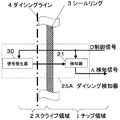
さらに、ダイシング検知器71の応用として、図3に示すものがある。ダイシング検知器71Aは、Vssをチップ領域1からシールリング3を越えてスクライブ領域2に引き出している所と、抵抗器72からシールリング3を越えてスクライブ領域2に引き出している所との距離を離し、その間のスクライブ領域2に検査用パッド50を複数配置し、スクライブ領域1からシールリング3を越えてチップ領域に引き込む配線や、シールリング3を越えてスクライブ領域2とチップ領域1を結ぶダミー配線73を挿入した構成にする。ダイシング検知器71Aでは、ますます経路の特定が困難となり不正な解析行為に対して耐タンパー性を向上させることができる。また、ダイシング検知器71と71Aの実施形態において、制御信号Dを省略して検知器70を常時有効にする構成でもかまわない。
(Application of dicing detector 71)
Further, an application of the dicing detector 71 is shown in FIG. The dicing detector 71A determines the distance between the place where Vss is drawn from the
(ダイシング検知器の第2実施形態)
次に、本発明による第2の実施形態によるダイシング検知器25について、図4の構成図を用いて説明する。第2のダイシング検知器25は、スクライブ領域2に配置された監視信号入力用パッド20と、監視信号入力用パッド20から信号が入力されるチップ領域1に配置された検知器21とで構成される。
(Second embodiment of dicing detector)
Next, a dicing detector 25 according to a second embodiment of the present invention will be described with reference to the configuration diagram of FIG. The second dicing detector 25 includes a monitoring
ダイシング検知器25の動作について説明する。半導体装置が半導体ウェハより切り出される前は、ウェハ検査時に監視信号入力用パッド20から任意の電気特性を有する監視信号が検知器21に入力され、制御信号Dにより、検知器21の検知タイミングを制御して、監視信号入力用パッド20より入力される任意の信号の電気特性を監視し、異常がなければ、ダイシングされていない状態の検知信号Aが出力される。
The operation of the dicing detector 25 will be described. Before the semiconductor device is cut out from the semiconductor wafer, a monitoring signal having arbitrary electrical characteristics is input from the monitoring
一方、ウェハ検査が終了し、ダイシングライン4に沿ってスクライブ領域2を切り落とすと、監視信号入力パッド20も一緒に切り落とされることにより、検知器21への監視信号入力が物理的に遮断される。検知器21は監視していた信号の電気特性の変化を捕捉して、半導体装置が半導体ウェハより切り出された状態の検出信号Aを出力する。偶然に監視入力信号と同一のものを外部から検知器21に与えない限り保護効力を無効にすることはできないので、監視入力信号は極力、固定電位等の単純なものにせずに、信号パターンや、高電圧・負電圧、パルスの位相差がある信号等の偶然性を含めても同一な電気特性を外部から与えることが容易でないものにすることにより、耐タンパー性が向上する。
On the other hand, when the wafer inspection is completed and the
(ダイシング検知器25の応用)
さらに、ダイシング検知器25の応用として、図5に示すように、ダイシング検知器25Aは監視用入力パッド20の代わりに信号発生器30を配置する。制御信号Dで、信号発生器30と検知器21を制御するように構成される。ウェハ検査時には信号発生器30から、信号を検知器21に与えることができるので、ダイシング検知器25に比べてウェハ検査時のパッド数が減ることになるので、それに伴うウェハ検査コストを下げることができる。
(Application of dicing detector 25)
Further, as an application of the dicing detector 25, as shown in FIG. 5, the dicing detector 25 </ b> A includes a
(ダイシング検知器の第3の実施形態)
図6に本発明による第3の実施形態によるダイシング検知器11の構成図を示す。ダイシング検知器11は、チップ領域1に配置された信号発生器5と、信号発生器5からシールリング3を越えてスクライブ領域2に引き出され、スクライブ領域2上を通り、再びシールリング3を越えてチップ領域1内に配線された監視配線7と、チップ領域1に配置された監視配線7の電気特性を監視する検知器8と、信号発生器5と検知器8を制御する制御回路6で構成される。
(Third embodiment of dicing detector)
FIG. 6 shows a configuration diagram of a dicing detector 11 according to a third embodiment of the present invention. The dicing detector 11 is pulled out from the
次にダイシング検知器11の動作を説明する。制御信号Dにより、制御回路6が起動し、制御回路6からの制御信号を受けて信号発生器5が任意のタイミングで所定の電気特性の信号を発生する。この信号を監視配線7と参照信号配線Bを通して、検知器8に送り、監視配線7と参照信号Bの電気特性の比較や照合が行う。そして、同一と判定した場合は、半導体装置はまだ半導体ウェハより切り出されていない状態の検知信号Aが出力され、相違と判定した場合は、半導体装置が半導体ウェハより切り出された状態の検知信号Aを出力する。ダイシング検知器11の耐タンパー性は、信号発生器から発生する信号を工夫することがより一層向上させることができる。例えば、監視配線7と参照信号Bの信号パターンの監視比較や、電気特性の監視比較、監視配線7と参照信号Bの配線物理特性の監視比較などが有効であり、さらに、これらの組み合わせで判定させるようにすると、ダイシング後、半導体装置に残った監視配線7を利用し、外部から信号を与える不正攻撃対し、正しい信号に一致させることが偶然性を含めてより一層困難となり効果的である。
Next, the operation of the dicing detector 11 will be described. In response to the control signal D, the
(ダイシング検知器11の応用1)
さらに、ダイシング検知器11の第1応用形態であるダイシング検知器11Aの構成を図7に示す。ダイシング検出器11Aでは、信号発生器5を乱数発生器10に置き換える構成にするとより耐タンパー性が向上する。ダイシング検知器11と11Aにおいて、参照信号Bの配線を観察により見つけ出し、参照信号Bを外部からプローブを立てて観測し、信号をトレースしたり、参照信号Bの配線をダイシング後、半導体装置に残った監視配線7にFIB加工技術や、バイパス線により接続したりする不正攻撃に対しては、監視配線7と参照信号Bの配線物理特性を監視比較する検知方式が有効であるが、それ以外の検知方式では、参照信号Bの配線を極力下層の配線層に配置し、その上層を他の配線が複数通るようにする。または、監視配線7には信号発生器5から生の信号を送り、参照信号Bはデコードした信号を送る。その後、検知器8で参照信号Bをエンコードして監視配線7から来た信号と比較する。または、信号発生器5で暗号化してから参照信号Bを出し、検知器8で復号化させる。あるいは、監視配線7にはパラレルで信号を送るが、参照信号Bはシリアルで信号を送る等、監視配線7と参照信号Bの信号形態や、配線の物理形状をかえるとさらに耐タンパー性が向上する。
(
Further, FIG. 7 shows a configuration of a dicing detector 11A which is a first application form of the dicing detector 11. In the dicing detector 11A, when the
(ダイシング検知器11の応用2)
図8はダイシング検知器11の第2応用形態であるダイシング検知器11Bの構成を示す。この構成ではさらに容易に耐タンパー性を向上させることができる。ダイシング検知器11とは、信号発生器5をスクライブ領域2に配置し、制御回路6からの信号発生器5への制御信号が、シールリング3を越えてスクライブ領域2上の信号発生器5に接続され、参照信号Bが、スクライブ領域2の検知器8から離れた場所からシールリング3を越えてチップ領域1に引き込み、検知器8に接続するところが異なる。ダイシングライン4に沿ってダイシングされると、信号発生器5と参照信号Bの配線が切り落とされるので、参照信号Bの観測は不可能である。さらに、半導体装置に残った監視配線7と参照信号Bの配線をFIB加工やその他導線により短絡して、外部より同一信号を送るという不正な解析攻撃が考えられるが、監視配線7と参照信号Bの配線がチップ領域1に引き込まれている場所の距離を離すことや、監視配線7と参照配線Bの信号携帯、あるいは配線の物理形態をかえることにより、容易に難易度を増すことができ、より容易に耐タンパー性を向上させることができる。
(
FIG. 8 shows a configuration of a dicing detector 11 </ b> B that is a second application form of the dicing detector 11. With this configuration, tamper resistance can be improved more easily. In the dicing detector 11, the
(ダイシング検知器の第4の実施形態)
次に本発明による第4の実施形態によるダイシング検知器を持つ半導体装置について、図9の構成図を用いて説明する。この半導体装置は、全てが第1から第3の実施形態のダイシング検知器のうちのいずれか1つのダイシング検知器90と、各々のダイシング検知器90からの検知信号A1の内容により検知判定を行う検知判定器91で構成される。以下に第4のダイシング検知器90を持つ半導体装置の動作について説明する。
(Fourth embodiment of dicing detector)
Next, a semiconductor device having a dicing detector according to a fourth embodiment of the present invention will be described with reference to the block diagram of FIG. In this semiconductor device, all of the dicing
複数のダイシング検知器90から出力された検出信号A1は、検知判定器91において、すべての検出信号A1が、半導体装置が半導体ウェハより切り出されていない状態を示すときのみ、検知信号Aが半導体装置が半導体ウェハより切り出されていない状態の信号として出力される。従って、1つでもダイシング検知器90が、半導体装置が半導体ウェハより切り出されている状態の検出信号A1を出力した時は、半導体装置が半導体ウェハより切り出されている状態の検知信号Aを出力する。
The detection signals A1 output from the plurality of dicing
このため、不正行為者は、複数のダイシング検知器90に対して同時に不正手段による攻撃を加えかつ、成功しなければ保護効力を無効にすることができなくなり、改竄が非常に困難となる。また複数のダイシング検知器90をそれぞれ、実施形態1〜3の違うものにすると、さらに、不正行為は困難となり、耐タンパー性が格段に向上する。さらには、ダイシング工程の信頼性においても、複数のダイシング検知器90のどれか1つが、半導体装置が半導体ウェハより切り出されている状態を検知すれば良いことになるので、極めて高い加工信頼性の歩留まりを提供できる。
For this reason, the fraudster cannot attack the plurality of dicing
(第2の実施形態)
次に本発明による第2の実施形態について、図10を用いて説明する。図10において半導体ウェハは、第1の実施形態に加えて、ダイシング検知器53の機能が正常かどうかを検査判定する故障診断器40を備え、検査対象回路52からダイシング検知器53と故障診断器40の制御を行う制御信号D1が入力され、ダイシング検知器53の検知信号Aが故障診断器40に接続され、故障診断器40からの故障検出信号B2が検査対象回路52に入力されている。
(Second Embodiment)
Next, a second embodiment according to the present invention will be described with reference to FIG. In FIG. 10, in addition to the first embodiment, the semiconductor wafer includes a failure diagnosing device 40 that determines whether or not the function of the dicing
次に以上のように構成された保護回路の動作を説明する。半導体装置の電源起動時に制御信号D1により、故障診断器40から、ダイシング検知器53に対して、検知機能を検査するため、ダイシング前の状態とダイシング後の状態の情報を検査用パターン(テスト信号)Cとして数回送り、ダイシング検知器53を動作させて検知信号Aを発生させて、故障診断機40で期待値と比較し、比較結果に応じて故障検出信号B2を出力する。検知信号Aと期待値とが一致した場合は、故障検出信号B2はダイシング検知器53が正常状態であることを検査対象回路52に伝え、前述の第1の実施形態と同じ動作をさせる。
Next, the operation of the protection circuit configured as described above will be described. In order to inspect the detection function from the failure diagnosing device 40 to the dicing
一方、不一致が検出された場合は、故障検出信号B2はダイシング検知器53が不具合の状態を示す信号となり、検知信号Aの状態いかんにかかわらず、検査対象回路52に伝えた故障検出信号B2により、半導体装置を安全モードに移行させる。上記実施形態においては、たとえ、不正行為者に検知信号Aの配線をつきとめられて、半導体装置が半導体ウェハより切り出されていない状態の信号を外部から適当な不正手段により与える攻撃に対しても保護効力を発揮し、格段に耐タンパー性を向上させた半導体装置および半導体ウェハを容易に提供できる。
On the other hand, when a mismatch is detected, the failure detection signal B2 is a signal indicating that the dicing
(第3の実施形態)
最後に本発明による第3の実施形態について、図11を用いて説明する。図11において半導体ウェハは、第1の実施形態に加えて、不揮発メモリ61の情報とダイシング検出器53からの検知信号Aの状態により、不揮発メモリ61の情報の読み出し/書き込みと、不正検知信号B1を出力するシーケンサー60を備え、検査対象回路52からダイシング検知器53とシーケンサー60と不揮発メモリ61の制御を行う制御信号D2が各々入力され、シーケンサー60の不正検知信号B1が、検査対象回路52に入力されている。
(Third embodiment)
Finally, a third embodiment according to the present invention will be described with reference to FIG. In FIG. 11, in addition to the first embodiment, the semiconductor wafer reads / writes information in the
次に以上のように構成された保護回路の動作を説明する。制御信号D2によりダイシング検知器53を動作させ、検知信号Aをシーケンサー60に送る。同様に、制御信号D2により、シーケンサー60と不揮発メモリ61を起動させて、不揮発メモリ61より情報をシーケンサー60に読み出す。シーケンサー60は読み出した不揮発メモリ61の情報がウェハ検査の状態(例えばオール0)で、かつダイシング検知器53からの検知信号Aの状態が、半導体装置が半導体ウェハより切り出されていない状態であれば、第1の実施形態での半導体装置が半導体ウェハより切り出されていない状態と同じ動作を行う。
Next, the operation of the protection circuit configured as described above will be described. The dicing
一方、ダイシング検知器53からの検知信号Aの状態が、半導体装置が半導体ウェハより切り出されている状態であれば、不揮発メモリ61から読み出した情報いかんにかかわらず、半導体装置が半導体ウェハより切り出されたという情報を不揮発メモリ61に書き込み、その後は、前述の本発明による第1の実施形態での半導体装置が半導体ウェハより切り出された状態と同じ動作を行う。
On the other hand, if the state of the detection signal A from the dicing
次に、不揮発メモリ61から読み出した情報が、半導体装置が半導体ウェハより切り出されたという情報である場合は、ダイシング検知器53からの検知信号Aの状態にかかわらず、不揮発メモリ61への書き込みは行わない。この時、ダイシング検知器53からの検知信号Aの状態が、半導体装置が半導体ウェハより切り出された状態であれば、前述の本発明による第1の実施形態での半導体装置が半導体ウェハより切り出された状態と同じ動作を行うが、違う場合には、シーケンサー60より不正検出信号B1出力し、半導体装置を安全モードに移行させる。
Next, when the information read from the
以上のことより、ウェハ検査時は、ダイシング検知器に従って保護するが、ウェハ検査後、半導体装置を半導体ウェハより切り出し、出荷前に一度半導体装置を動作させて不揮発メモリに出荷状態の情報を書き込んでから出荷すると、不揮発メモリの情報が書きかわらない限り、ダイシング検知器がどのような不正な手段で無効化をされようが完全に保護され耐タンパー性は格段に向上する。 As described above, during wafer inspection, protection is performed according to a dicing detector, but after wafer inspection, the semiconductor device is cut out from the semiconductor wafer, and the semiconductor device is operated once before shipment, and shipping state information is written in the nonvolatile memory. As long as the information in the non-volatile memory is not rewritten, the dicing detector is completely protected from being invalidated by any unauthorized means, and the tamper resistance is remarkably improved.
以上のことから、本発明による半導体ウェハによれば、パッドからの引き出し配線を利用したいかなる不正な解析手段を用いても、保護効力を発揮でき、ダイシング工程の前後に特別な製造工程を付加することなく容易に提供できる。 From the above, according to the semiconductor wafer according to the present invention, the protection effect can be exerted by using any unauthorized analysis means using the lead wiring from the pad, and a special manufacturing process is added before and after the dicing process. Can be easily provided.
本発明の半導体ウェハは、スクライブ領域の切断後に、切断を検知する検知手段と、検査パッドからの引き込み線の電位を切り替える切り替え手段と前記切り替え手段と検査対象回路間の電位異常を検知して検査対象回路を安全モードに移行させることで、スクライブ領域切断後のパッドからの引き込み配線を利用した不正解析を防ぐことができるという効果を有し、半導体装置内部の機密情報を不正な手段により、解析・改竄から保護することを目的とする保護機能を備えた半導体ウェハ等として有用である。 The semiconductor wafer of the present invention is inspected by detecting a detecting means for detecting the cutting after the cutting of the scribe area, a switching means for switching the potential of the lead-in line from the inspection pad, and a potential abnormality between the switching means and the circuit to be inspected. By shifting the target circuit to the safe mode, it is possible to prevent unauthorized analysis using the lead-in wiring from the pad after cutting the scribe area, and analyze confidential information inside the semiconductor device by unauthorized means -It is useful as a semiconductor wafer having a protection function for the purpose of protecting it from tampering.
1 チップ領域
2 スクライブ領域
4 ダイシングライン
5、30 信号発生器
6 制御回路
7 監視配線
8、21、55、70 検知器
10 乱数発生器
11、11A、11B、25、25A、53、71、71A、90 ダイシング検知器
20 監視信号入力用パッド
40 故障診断器
50 検査用パッド
51 切り替え回路
52 検査対象回路
54 入出力経路
60 シーケンサ
61 不揮発性メモリ
72 抵抗器
73 ダミー配線
81 MOSトランジスタ
82 金属配線
83 制御用PAD
91 検知判定器
A 検知信号
A1 検出信号
B 参照信号
B1、E 不正検出信号
B2 故障検出信号
C 検査用パターン
D、D1、D2 制御信号
DESCRIPTION OF
91 Detection and decision device A Detection signal A1 Detection signal B Reference signal B1, E Fraud detection signal B2 Failure detection signal C Inspection pattern D, D1, D2 Control signal
Claims (11)
前記スクライブ領域の切断を検知する検知手段と、
前記スクライブ領域が切断された場合に前記検査対象回路と前記検査対象回路に対する検査用パッド間を固定電位に切り替える切替手段と、
前記切替手段と前記検査対象回路間の電位異常を検知して前記検査対象回路を安全モードに移行させるモード移行手段と、
を備え、
前記モード移行手段は、前記検査対象回路に入力される検査モードコマンドを拒否する機能である半導体ウェハ。 A semiconductor wafer in which a plurality of semiconductor devices including a circuit to be inspected are arranged via a scribe region,
Detecting means for detecting cutting of the scribe region;
Switching means for switching between the inspection object circuit and the inspection pad for the inspection object circuit to a fixed potential when the scribe region is cut;
A mode transition means for detecting a potential abnormality between the switching means and the circuit to be inspected and causing the circuit to be inspected to transition to a safety mode;
Equipped with a,
The mode shift means is a semiconductor wafer having a function of rejecting an inspection mode command input to the inspection target circuit .
前記スクライブ領域に配置された監視信号入力用パッド、及び
前記監視信号入力用パッドと前記スクライブ領域を跨いで前記半導体装置内に配置された前記検知手段とを接続する監視配線を備え、
前記監視配線で前記監視信号入力用パッドからの特性変化を検知することを、特徴とする請求項1記載の半導体ウェハ。 It said detection means,
Placed before Symbol scribe region surveillance signal input pad, and
A monitoring wiring for connecting the monitoring signal input pad and the detection means disposed in the semiconductor device across the scribe region ;
2. The semiconductor wafer according to claim 1 , wherein a change in characteristics from the monitoring signal input pad is detected by the monitoring wiring .
前記スクライブ領域に配置された信号発生手段、及び
前記信号発生手段と前記スクライブ領域を跨いで前記半導体装置内に配置された検知回路とを接続する監視配線を備え、
前記信号発生手段により、前記監視配線に任意特性の信号を与え、
前記検知手段により、前記監視配線の特性変化を検知することを特徴とする請求項1記載の半導体ウェハ。 It said detection means,
Signal generating hand stage and, arranged in front Symbol scribe region
A monitoring wire connecting the detection knowledge circuitry disposed within the semiconductor device across the scribe area and the signal generating means,
The signal generating means gives a signal of arbitrary characteristics to the monitoring wiring,
2. The semiconductor wafer according to claim 1 , wherein a change in characteristics of the monitoring wiring is detected by the detection means .
前記半導体装置内に配置された信号発生手段、
前記信号発生手段と前記スクライブ領域を跨いで前記半導体装置内に配置された前記検知手段とを接続する監視配線、及び
前記半導体装置内において、前記信号発生手段と前記検知手段とを接続する参照信号配線を備え
前記信号発生手段により、前記監視配線に任意特性の信号と前記参照信号配線に前記スクライブ領域の切断を検知するための参照信号とを与え、
前記検知手段により、前記参照信号に対する前記監視配線の特性異常を検知することを、特徴とする請求項1記載の半導体ウェハ。 It said detection means,
Signal generating hand stage arranged before Symbol in the semiconductor device,
A monitoring wiring for connecting the signal generating means and the detecting means arranged in the semiconductor device across the scribe region ; and
In the semiconductor device, a reference signal wiring for connecting the signal generation means and the detection means is provided.
The signal generating means gives an arbitrary characteristic signal to the monitoring wiring and a reference signal for detecting cutting of the scribe region to the reference signal wiring,
The semiconductor wafer according to claim 1 , wherein the detection unit detects a characteristic abnormality of the monitoring wiring with respect to the reference signal .
前記半導体装置内に配置された信号発生手段、
前記信号発生手段と前記スクライブ領域を跨いで前記半導体装置内に配置された前記検知手段とを接続する監視配線、及び
前記スクライブ領域を跨いで前記信号発生手段と前記検知手段とを接続する参照信号配線を備え、
前記信号発生手段により、
前記監視配線に任意特性の信号と、
前記参照配線に前記スクライブ領域の切断を検知するための参照信号とを与え、
前記検知手段により、前記参照信号に対する前記監視配線の特性異常を検知することを、特徴とする請求項1記載の半導体ウェハ。 The detection means includes
A signal generating means disposed in the semiconductor device;
A monitoring wiring for connecting the signal generating means and the detecting means arranged in the semiconductor device across the scribe region; and
A reference signal wiring for connecting the signal generating means and the detecting means across the scribe region,
By the signal generating means,
A signal of arbitrary characteristics in the monitoring wiring,
Giving a reference signal for detecting the cutting of the scribe region to the reference wiring,
The semiconductor wafer according to claim 1 , wherein the detection unit detects a characteristic abnormality of the monitoring wiring with respect to the reference signal.
Priority Applications (4)
| Application Number | Priority Date | Filing Date | Title |
|---|---|---|---|
| JP2003387974A JP4462903B2 (en) | 2003-11-18 | 2003-11-18 | Semiconductor wafer |
| EP04027293A EP1533842A3 (en) | 2003-11-18 | 2004-11-17 | Semiconductor device with protection against unauthorized analysis |
| CNB2004100104789A CN1320640C (en) | 2003-11-18 | 2004-11-18 | Semiconductor wafer |
| US10/990,545 US7242080B2 (en) | 2003-11-18 | 2004-11-18 | Semiconductor wafer with information protection function |
Applications Claiming Priority (1)
| Application Number | Priority Date | Filing Date | Title |
|---|---|---|---|
| JP2003387974A JP4462903B2 (en) | 2003-11-18 | 2003-11-18 | Semiconductor wafer |
Publications (2)
| Publication Number | Publication Date |
|---|---|
| JP2005150514A JP2005150514A (en) | 2005-06-09 |
| JP4462903B2 true JP4462903B2 (en) | 2010-05-12 |
Family
ID=34431543
Family Applications (1)
| Application Number | Title | Priority Date | Filing Date |
|---|---|---|---|
| JP2003387974A Expired - Fee Related JP4462903B2 (en) | 2003-11-18 | 2003-11-18 | Semiconductor wafer |
Country Status (4)
| Country | Link |
|---|---|
| US (1) | US7242080B2 (en) |
| EP (1) | EP1533842A3 (en) |
| JP (1) | JP4462903B2 (en) |
| CN (1) | CN1320640C (en) |
Families Citing this family (13)
| Publication number | Priority date | Publication date | Assignee | Title |
|---|---|---|---|---|
| US8588511B2 (en) * | 2002-05-22 | 2013-11-19 | Cognex Corporation | Method and apparatus for automatic measurement of pad geometry and inspection thereof |
| JP4274576B2 (en) | 2007-01-12 | 2009-06-10 | エルピーダメモリ株式会社 | Semiconductor device |
| US7888776B2 (en) * | 2008-06-30 | 2011-02-15 | Texas Instruments Incorporated | Capacitor-based method for determining and characterizing scribe seal integrity and integrity loss |
| US8513970B2 (en) | 2008-12-26 | 2013-08-20 | Nec Corporation | Semiconductor device and method of testing the same |
| CN101950332B (en) * | 2010-07-12 | 2012-08-29 | 大唐微电子技术有限公司 | Chip protecting method and system |
| WO2014045989A1 (en) * | 2012-09-20 | 2014-03-27 | ピーエスフォー ルクスコ エスエイアールエル | Semiconductor wafer, semiconductor device, and method for manufacturing semiconductor device |
| CN103279704B (en) * | 2013-06-08 | 2016-12-07 | 大唐微电子技术有限公司 | A kind of chip makes physical integrity detection device and system |
| CN103440452B (en) * | 2013-08-20 | 2016-01-06 | 大唐微电子技术有限公司 | A kind of chip makes physical integrity detection device |
| FR3084520B1 (en) | 2018-07-25 | 2020-08-14 | Stmicroelectronics Rousset | PROTECTION METHOD FOR AN INTEGRATED CIRCUIT, AND CORRESPONDING DEVICE |
| FR3084521B1 (en) * | 2018-07-25 | 2020-08-14 | Stmicroelectronics Rousset | PROTECTION PROCESS OF AN INTEGRATED CIRCUIT MODULE AND CORRESPONDING DEVICE |
| FR3084492A1 (en) | 2018-07-30 | 2020-01-31 | Stmicroelectronics (Rousset) Sas | METHOD FOR DETECTING AN ATTACK BY A BEAM OF ELECTRICALLY CHARGED PARTICLES ON AN INTEGRATED CIRCUIT, AND CORRESPONDING INTEGRATED CIRCUIT |
| FR3099259B1 (en) | 2019-07-24 | 2021-08-13 | St Microelectronics Rousset | Method for protecting data stored in a memory, and corresponding integrated circuit |
| CN112071768B (en) * | 2020-09-04 | 2022-09-20 | 晶能光电(江西)有限公司 | P-surface process monitoring structure and method and wafer structure |
Family Cites Families (16)
| Publication number | Priority date | Publication date | Assignee | Title |
|---|---|---|---|---|
| JPS55135759A (en) * | 1979-04-11 | 1980-10-22 | Nec Corp | Diagnostic unit |
| JPH0480936A (en) * | 1990-07-24 | 1992-03-13 | Seiko Epson Corp | Semiconductor device |
| CN2134785Y (en) * | 1992-04-10 | 1993-06-02 | 黄宾来 | Cosy ash-tray |
| JPH06230086A (en) * | 1992-09-22 | 1994-08-19 | Nec Corp | Lsi testing circuit |
| US5861652A (en) * | 1996-03-28 | 1999-01-19 | Symbios, Inc. | Method and apparatus for protecting functions imbedded within an integrated circuit from reverse engineering |
| JPH11272509A (en) * | 1998-03-24 | 1999-10-08 | Nec Ic Microcomput Syst Ltd | Semiconductor integrated circuit |
| JP4234244B2 (en) * | 1998-12-28 | 2009-03-04 | 富士通マイクロエレクトロニクス株式会社 | Wafer level package and semiconductor device manufacturing method using wafer level package |
| JP2001135597A (en) | 1999-08-26 | 2001-05-18 | Fujitsu Ltd | Method for manufacturing semiconductor device |
| US7005733B2 (en) * | 1999-12-30 | 2006-02-28 | Koemmerling Oliver | Anti tamper encapsulation for an integrated circuit |
| JP3553457B2 (en) * | 2000-03-31 | 2004-08-11 | シャープ株式会社 | Semiconductor device and manufacturing method thereof |
| JP2002033361A (en) * | 2000-07-17 | 2002-01-31 | Mitsumi Electric Co Ltd | Semiconductor wafer |
| JP2002217258A (en) * | 2001-01-22 | 2002-08-02 | Hitachi Ltd | Semiconductor device, method for measurement of it and manufacturing method for semiconductor device |
| JP3506377B2 (en) | 2001-04-09 | 2004-03-15 | 松下電器産業株式会社 | Semiconductor device and manufacturing method thereof |
| JP4034992B2 (en) * | 2002-05-01 | 2008-01-16 | 松下電器産業株式会社 | Semiconductor device |
| JP3748857B2 (en) * | 2002-01-25 | 2006-02-22 | 松下電器産業株式会社 | Semiconductor integrated circuit and data carrier equipped with the same |
| JP2003218178A (en) * | 2002-01-25 | 2003-07-31 | Matsushita Electric Ind Co Ltd | Semiconductor device and semiconductor chip |
-
2003
- 2003-11-18 JP JP2003387974A patent/JP4462903B2/en not_active Expired - Fee Related
-
2004
- 2004-11-17 EP EP04027293A patent/EP1533842A3/en not_active Withdrawn
- 2004-11-18 US US10/990,545 patent/US7242080B2/en active Active
- 2004-11-18 CN CNB2004100104789A patent/CN1320640C/en not_active Expired - Fee Related
Also Published As
| Publication number | Publication date |
|---|---|
| CN1627505A (en) | 2005-06-15 |
| CN1320640C (en) | 2007-06-06 |
| JP2005150514A (en) | 2005-06-09 |
| US7242080B2 (en) | 2007-07-10 |
| US20050104161A1 (en) | 2005-05-19 |
| EP1533842A3 (en) | 2006-02-08 |
| EP1533842A2 (en) | 2005-05-25 |
Similar Documents
| Publication | Publication Date | Title |
|---|---|---|
| JP4462903B2 (en) | Semiconductor wafer | |
| US20200349295A1 (en) | Tamper detection countermeasures to deter physical attack on a security asic | |
| JP4748929B2 (en) | Protection circuit and semiconductor device | |
| US20230036441A1 (en) | Protective semiconductor elements for bonded structures | |
| KR100508891B1 (en) | Circuit arrangement and a method for detecting an undesired attack on an integrated circuit | |
| US8089285B2 (en) | Implementing tamper resistant integrated circuit chips | |
| US5389738A (en) | Tamperproof arrangement for an integrated circuit device | |
| KR100710936B1 (en) | Protection circuit for an integrated circuit | |
| JP5387144B2 (en) | Malfunction occurrence attack detection circuit and integrated circuit | |
| US6798234B2 (en) | Apparatus for protecting an integrated circuit formed in a substrate and method for protecting the circuit against reverse engineering | |
| JPH0787237B2 (en) | Integrated circuit chip | |
| WO2011155114A1 (en) | Protection circuit, semiconductor device and electronic equipment | |
| TW201600998A (en) | Method and apparatus for detecting fault injection | |
| US20060180939A1 (en) | Tamper-resistant semiconductor device | |
| US6359338B1 (en) | Semiconductor apparatus with self-security function | |
| NO304628B1 (en) | Integrated circuit chip to prevent change of secured data stored in a predetermined storage position | |
| JP2007035729A (en) | Semiconductor integrated circuit device | |
| JP4836995B2 (en) | Integrated circuit module | |
| US10216452B2 (en) | Breach detection in integrated circuits | |
| JP4181068B2 (en) | Integrated circuit module | |
| Jacob | How could device security against unauthorized internal chip access be married with design for testability? | |
| JP2004079150A (en) | Semiconductor device | |
| JPH056700A (en) | Circuit for detecting data erroneously read from eprom | |
| JPH0460731A (en) | Protective system for storage content |
Legal Events
| Date | Code | Title | Description |
|---|---|---|---|
| RD04 | Notification of resignation of power of attorney |
Free format text: JAPANESE INTERMEDIATE CODE: A7424 Effective date: 20060327 |
|
| A621 | Written request for application examination |
Free format text: JAPANESE INTERMEDIATE CODE: A621 Effective date: 20060929 |
|
| RD02 | Notification of acceptance of power of attorney |
Free format text: JAPANESE INTERMEDIATE CODE: A7422 Effective date: 20071114 |
|
| RD04 | Notification of resignation of power of attorney |
Free format text: JAPANESE INTERMEDIATE CODE: A7424 Effective date: 20071121 |
|
| RD02 | Notification of acceptance of power of attorney |
Free format text: JAPANESE INTERMEDIATE CODE: A7422 Effective date: 20071128 |
|
| RD04 | Notification of resignation of power of attorney |
Free format text: JAPANESE INTERMEDIATE CODE: A7424 Effective date: 20071205 |
|
| RD04 | Notification of resignation of power of attorney |
Free format text: JAPANESE INTERMEDIATE CODE: A7424 Effective date: 20071212 |
|
| A131 | Notification of reasons for refusal |
Free format text: JAPANESE INTERMEDIATE CODE: A131 Effective date: 20091027 |
|
| A977 | Report on retrieval |
Free format text: JAPANESE INTERMEDIATE CODE: A971007 Effective date: 20091029 |
|
| A521 | Request for written amendment filed |
Free format text: JAPANESE INTERMEDIATE CODE: A523 Effective date: 20091216 |
|
| TRDD | Decision of grant or rejection written | ||
| A01 | Written decision to grant a patent or to grant a registration (utility model) |
Free format text: JAPANESE INTERMEDIATE CODE: A01 Effective date: 20100119 |
|
| A01 | Written decision to grant a patent or to grant a registration (utility model) |
Free format text: JAPANESE INTERMEDIATE CODE: A01 |
|
| A61 | First payment of annual fees (during grant procedure) |
Free format text: JAPANESE INTERMEDIATE CODE: A61 Effective date: 20100216 |
|
| FPAY | Renewal fee payment (event date is renewal date of database) |
Free format text: PAYMENT UNTIL: 20130226 Year of fee payment: 3 |
|
| R150 | Certificate of patent or registration of utility model |
Ref document number: 4462903 Country of ref document: JP Free format text: JAPANESE INTERMEDIATE CODE: R150 Free format text: JAPANESE INTERMEDIATE CODE: R150 |
|
| FPAY | Renewal fee payment (event date is renewal date of database) |
Free format text: PAYMENT UNTIL: 20130226 Year of fee payment: 3 |
|
| FPAY | Renewal fee payment (event date is renewal date of database) |
Free format text: PAYMENT UNTIL: 20140226 Year of fee payment: 4 |
|
| R250 | Receipt of annual fees |
Free format text: JAPANESE INTERMEDIATE CODE: R250 |
|
| S111 | Request for change of ownership or part of ownership |
Free format text: JAPANESE INTERMEDIATE CODE: R313113 |
|
| R350 | Written notification of registration of transfer |
Free format text: JAPANESE INTERMEDIATE CODE: R350 |
|
| LAPS | Cancellation because of no payment of annual fees |