JP4450016B2 - Liquid crystal display device and liquid crystal driving circuit - Google Patents
Liquid crystal display device and liquid crystal driving circuit Download PDFInfo
- Publication number
- JP4450016B2 JP4450016B2 JP2007155274A JP2007155274A JP4450016B2 JP 4450016 B2 JP4450016 B2 JP 4450016B2 JP 2007155274 A JP2007155274 A JP 2007155274A JP 2007155274 A JP2007155274 A JP 2007155274A JP 4450016 B2 JP4450016 B2 JP 4450016B2
- Authority
- JP
- Japan
- Prior art keywords
- voltage
- liquid crystal
- image data
- pixel
- driving
- Prior art date
- Legal status (The legal status is an assumption and is not a legal conclusion. Google has not performed a legal analysis and makes no representation as to the accuracy of the status listed.)
- Expired - Fee Related
Links
Images


Classifications
-
- G—PHYSICS
- G09—EDUCATION; CRYPTOGRAPHY; DISPLAY; ADVERTISING; SEALS
- G09G—ARRANGEMENTS OR CIRCUITS FOR CONTROL OF INDICATING DEVICES USING STATIC MEANS TO PRESENT VARIABLE INFORMATION
- G09G3/00—Control arrangements or circuits, of interest only in connection with visual indicators other than cathode-ray tubes
- G09G3/20—Control arrangements or circuits, of interest only in connection with visual indicators other than cathode-ray tubes for presentation of an assembly of a number of characters, e.g. a page, by composing the assembly by combination of individual elements arranged in a matrix no fixed position being assigned to or needed to be assigned to the individual characters or partial characters
- G09G3/34—Control arrangements or circuits, of interest only in connection with visual indicators other than cathode-ray tubes for presentation of an assembly of a number of characters, e.g. a page, by composing the assembly by combination of individual elements arranged in a matrix no fixed position being assigned to or needed to be assigned to the individual characters or partial characters by control of light from an independent source
- G09G3/36—Control arrangements or circuits, of interest only in connection with visual indicators other than cathode-ray tubes for presentation of an assembly of a number of characters, e.g. a page, by composing the assembly by combination of individual elements arranged in a matrix no fixed position being assigned to or needed to be assigned to the individual characters or partial characters by control of light from an independent source using liquid crystals
- G09G3/3611—Control of matrices with row and column drivers
- G09G3/3674—Details of drivers for scan electrodes
- G09G3/3677—Details of drivers for scan electrodes suitable for active matrices only
-
- G—PHYSICS
- G09—EDUCATION; CRYPTOGRAPHY; DISPLAY; ADVERTISING; SEALS
- G09G—ARRANGEMENTS OR CIRCUITS FOR CONTROL OF INDICATING DEVICES USING STATIC MEANS TO PRESENT VARIABLE INFORMATION
- G09G3/00—Control arrangements or circuits, of interest only in connection with visual indicators other than cathode-ray tubes
- G09G3/20—Control arrangements or circuits, of interest only in connection with visual indicators other than cathode-ray tubes for presentation of an assembly of a number of characters, e.g. a page, by composing the assembly by combination of individual elements arranged in a matrix no fixed position being assigned to or needed to be assigned to the individual characters or partial characters
- G09G3/34—Control arrangements or circuits, of interest only in connection with visual indicators other than cathode-ray tubes for presentation of an assembly of a number of characters, e.g. a page, by composing the assembly by combination of individual elements arranged in a matrix no fixed position being assigned to or needed to be assigned to the individual characters or partial characters by control of light from an independent source
- G09G3/36—Control arrangements or circuits, of interest only in connection with visual indicators other than cathode-ray tubes for presentation of an assembly of a number of characters, e.g. a page, by composing the assembly by combination of individual elements arranged in a matrix no fixed position being assigned to or needed to be assigned to the individual characters or partial characters by control of light from an independent source using liquid crystals
- G09G3/3611—Control of matrices with row and column drivers
- G09G3/3648—Control of matrices with row and column drivers using an active matrix
-
- G—PHYSICS
- G09—EDUCATION; CRYPTOGRAPHY; DISPLAY; ADVERTISING; SEALS
- G09G—ARRANGEMENTS OR CIRCUITS FOR CONTROL OF INDICATING DEVICES USING STATIC MEANS TO PRESENT VARIABLE INFORMATION
- G09G2300/00—Aspects of the constitution of display devices
- G09G2300/08—Active matrix structure, i.e. with use of active elements, inclusive of non-linear two terminal elements, in the pixels together with light emitting or modulating elements
- G09G2300/0876—Supplementary capacities in pixels having special driving circuits and electrodes instead of being connected to common electrode or ground; Use of additional capacitively coupled compensation electrodes
-
- G—PHYSICS
- G09—EDUCATION; CRYPTOGRAPHY; DISPLAY; ADVERTISING; SEALS
- G09G—ARRANGEMENTS OR CIRCUITS FOR CONTROL OF INDICATING DEVICES USING STATIC MEANS TO PRESENT VARIABLE INFORMATION
- G09G2320/00—Control of display operating conditions
- G09G2320/02—Improving the quality of display appearance
- G09G2320/0252—Improving the response speed
-
- G—PHYSICS
- G09—EDUCATION; CRYPTOGRAPHY; DISPLAY; ADVERTISING; SEALS
- G09G—ARRANGEMENTS OR CIRCUITS FOR CONTROL OF INDICATING DEVICES USING STATIC MEANS TO PRESENT VARIABLE INFORMATION
- G09G2320/00—Control of display operating conditions
- G09G2320/10—Special adaptations of display systems for operation with variable images
- G09G2320/103—Detection of image changes, e.g. determination of an index representative of the image change
Description
本発明は、補助容量素子を含んで構成された液晶表示装置、およびそのような液晶表示装置に適用される液晶駆動回路に関する。 The present invention relates to a liquid crystal display device including an auxiliary capacitance element, and a liquid crystal driving circuit applied to such a liquid crystal display device.
近年、液晶を用いた表示素子(液晶素子)を駆動することによって映像表示を行う液晶表示装置が広く活用されている。このような液晶表示装置では、ガラス等の基板間に封止した液晶層において、液晶分子の配列を変化させることにより光源からの光を透過、変調させて表示を行っている。 2. Description of the Related Art In recent years, liquid crystal display devices that display images by driving display elements (liquid crystal elements) that use liquid crystals have been widely used. In such a liquid crystal display device, display is performed by transmitting and modulating light from a light source by changing the arrangement of liquid crystal molecules in a liquid crystal layer sealed between substrates such as glass.
また、このような液晶表示装置では、従来より、液晶素子に対する印加電圧の変化が大きい場合には、画像データに基づく電圧に対して所定のオーバードライブ電圧を付加することにより(オーバードライブ駆動)、液晶の応答速度を向上させるようになっている(例えば、特許文献1)。 Further, in such a liquid crystal display device, when a change in the applied voltage to the liquid crystal element is conventionally large, by adding a predetermined overdrive voltage to the voltage based on the image data (overdrive driving), The response speed of the liquid crystal is improved (for example, Patent Document 1).
なお、これとは別の技術として、液晶表示装置の各画素に液晶素子への印加電圧を安定化させるための補助容量素子を形成すると共に、この補助容量素子の両端間の電圧を変化させることによって液晶素子の両端間の電圧をも変化させるようにしたもの(Cs on gate方式)が提案されている(例えば、特許文献2)。 As another technique, an auxiliary capacitance element for stabilizing the voltage applied to the liquid crystal element is formed in each pixel of the liquid crystal display device, and the voltage across the auxiliary capacitance element is changed. (Cs on gate method) in which the voltage across the liquid crystal element is also changed is proposed (for example, Patent Document 2).
ここで、従来の液晶表示装置では、駆動素子(TFT(Thin Film Transistor:薄膜トランジスタ)素子)の耐圧よりも高い電圧を液晶素子に印加することはできないことから、例えば黒表示状態から白表示状態への遷移や白表示状態から黒表示状態への遷移の際には、上記のようなオーバードライブ電圧を付加することができず、結果として中間階調付近での遷移にのみ、オーバードライブ駆動が適用されていた。すなわち、最も電圧の変化の大きい遷移の際にオーバードライブ電圧の付加ができないことから、本来最も液晶の応答速度を上げる必要のある場合にオーバードライブ駆動の適用ができず、液晶の応答速度の改善が不十分であった。 Here, in the conventional liquid crystal display device, since a voltage higher than the withstand voltage of a driving element (TFT (Thin Film Transistor) element) cannot be applied to the liquid crystal element, for example, from a black display state to a white display state. The overdrive voltage as described above cannot be added at the transition from the white display state to the black display state, and as a result, the overdrive drive is applied only to the transition near the middle gradation. It had been. In other words, since overdrive voltage cannot be applied at the time of the transition with the largest voltage change, overdrive drive cannot be applied when it is necessary to increase the response speed of the liquid crystal most, and the response speed of the liquid crystal is improved. Was insufficient.
なお、電源電圧および駆動素子の耐圧自体を本来よりも高く設定するようにすれば、その分だけ高い電圧を液晶素子に印加することが可能となり、液晶の応答速度も向上するが、それに伴って消費電力が増加したり発熱量が増えてしまい、駆動素子の信頼性の低下などの問題が生じてしまうことになる。 If the power supply voltage and the withstand voltage of the driving element are set higher than the original voltage, a higher voltage can be applied to the liquid crystal element and the response speed of the liquid crystal is improved. Power consumption increases or the amount of heat generated increases, causing problems such as a decrease in the reliability of the drive element.
このように従来の技術では、駆動素子の耐圧を上げることなく液晶の応答速度を向上させることが困難であり、改善の余地があった。 As described above, in the conventional technique, it is difficult to improve the response speed of the liquid crystal without increasing the breakdown voltage of the driving element, and there is room for improvement.
本発明はかかる問題点に鑑みてなされたもので、その目的は、駆動素子の耐圧を上げることなく液晶の応答速度を向上させることが可能な液晶表示装置および液晶駆動回路を提供することにある。 The present invention has been made in view of the above problems, that the aim is to provide a liquid crystal display device and a liquid clear dynamic circuit capable of improving the response speed of the liquid crystal without increasing the withstand voltage of the drive element It is in.
本発明の液晶表示装置は、マトリクス状に配置され、それぞれが、TFT素子と、主容量素子としての液晶素子と、補助容量素子とを含む複数の画素と、駆動対象の画素を線順次で選択し、選択した画素のTFT素子を所定のオン電圧により選択的にオン状態にすると共に、TFT素子を所定のオフ電圧により選択的にオフ状態にするための複数のゲート線と、駆動対象の画素に対し、TFT素子を介して画像データを供給するための複数のソース線と、各ゲート線の隣接ゲート線におけるオフ電圧を、画像データの輝度レベルに依存せずに一律に時間変化させつつ線順次動作を行うことにより、画素の表示駆動を行う駆動手段とを備えたものである。ここで、上記液晶素子は、その一端がTFT素子の一端に接続されている。また、上記補助容量素子は、その一端がTFT素子の一端に接続されると共に、他端が隣接ゲート線に接続されている。また、上記駆動手段は、現在の単位フレームの画像データとその直前の単位フレームの画像データとに基づいて、それらの画像データの輝度レベル差が所定の閾値未満の画素に対し、現在の単位フレームにおいて通常駆動による表示駆動を行うと判定する一方、上記輝度レベル差が上記閾値以上の画素に対し、現在の単位フレームにおいてオーバードライブ駆動による表示駆動を行うと判定する判定手段と、通常駆動による表示駆動を行うと判定された画素については、現在の単位フレームの画像データを、その輝度レベルが所定の分だけ下がるように補正する一方、オーバードライブ駆動による表示駆動を行うと判定された画素については、現在の単位フレームの画像データを、その直前の単位フレームと現在の単位フレームとの間での液晶素子の両端間電圧の変化が増加すると共に上記輝度レベル差が大きくなるのに応じて両端間電圧の変化がより大きくなるような画像データに補正する補正手段と、この補正手段による補正後の画像データを基に、表示駆動を画素ごと実施する駆動ドライバとを有している。また、上記補正手段は、通常駆動による表示駆動を行うと判定された画素については、補正後の画像データに基づいて液晶素子の両端間に電圧を印加しこれが安定した後の状態における輝度レベルが、補正前の画像データに基づいて液晶素子の両端間に電圧を印加した直後における輝度レベルと同等となるように、現在の単位フレームの画像データを補正し、オーバードライブ駆動による表示駆動を行うと判定された画素のうち、黒表示状態から白表示状態へ遷移する画素については、現在の単位フレームの画像データをそのまま補正後の画像データとして出力し、オーバードライブ駆動による表示駆動を行うと判定された画素のうち、白表示状態から黒表示状態へ遷移する画素については、通常駆動による表示駆動の際の補正よりも輝度レベルが過剰に下がるように、現在の単位フレームの画像データを補正するようになっている。 The liquid crystal display device of the present invention is arranged in a matrix form, and each selects a plurality of pixels including a TFT element, a liquid crystal element as a main capacitor element, and an auxiliary capacitor element, and a pixel to be driven in a line sequential manner. A plurality of gate lines for selectively turning on the TFT element of the selected pixel with a predetermined on-voltage, and selectively turning off the TFT element with a predetermined off-voltage, and a pixel to be driven In contrast, a plurality of source lines for supplying image data via TFT elements and off-voltages at adjacent gate lines of each gate line are changed while changing the time uniformly without depending on the luminance level of the image data. And a driving unit that performs display driving of the pixels by sequentially performing operations . Here, one end of the liquid crystal element is connected to one end of the TFT element. The auxiliary capacitance element has one end connected to one end of the TFT element and the other end connected to the adjacent gate line. Further, the driving means is configured to apply the current unit frame to a pixel whose luminance level difference is less than a predetermined threshold based on the image data of the current unit frame and the image data of the previous unit frame. And determining means for determining that display driving by overdrive is performed in a current unit frame for a pixel whose luminance level difference is equal to or greater than the threshold value, and displaying by normal driving For pixels determined to be driven, the image data of the current unit frame is corrected so that the luminance level is lowered by a predetermined amount, while for pixels determined to be displayed by overdrive driving. , The image data of the current unit frame is changed between the previous unit frame and the current unit frame. Correction means for correcting the image data so that the change in the voltage between both ends increases as the change in the voltage across the element increases and the brightness level difference increases, and the image corrected by the correction means And a drive driver that performs display drive for each pixel based on the data. The correction means applies a voltage across the liquid crystal element based on the corrected image data for the pixel determined to perform display driving by normal driving, and the luminance level in a state after this is stabilized When the image data of the current unit frame is corrected so as to be equal to the luminance level immediately after the voltage is applied between both ends of the liquid crystal element based on the image data before correction, and display driving by overdrive driving is performed. Among the determined pixels, for the pixels that transition from the black display state to the white display state, it is determined that the image data of the current unit frame is output as it is as the corrected image data, and display drive by overdrive drive is performed. For the pixels that transition from the white display state to the black display state, the luminance level is higher than the correction during display drive by normal drive. Le As falls over, so as to correct the image data of the current unit frame.
本発明の液晶駆動回路は、マトリクス状に配置されそれぞれがTFT素子と主容量素子としての液晶素子と補助容量素子とを含む複数の画素と、駆動対象の画素を線順次で選択しこの選択した画素のTFT素子を所定のオン電圧により選択的にオン状態にすると共にTFT素子を所定のオフ電圧により選択的にオフ状態にするための複数のゲート線と、駆動対象の画素に対しTFT素子を介して画像データを供給するための複数のソース線とを備え、上記液晶素子の一端がTFT素子の一端に接続され、上記補助容量素子の一端がTFT素子の一端に接続されると共に他端が隣接ゲート線に接続されるように構成された液晶表示装置に対して適用され、各ゲート線の隣接ゲート線におけるオフ電圧を画像データの輝度レベルに依存せずに一律に時間変化させつつ線順次動作を行うことにより画素の表示駆動を行うものであって、上記判定手段と、上記補正手段と、上記駆動ドライバとを備えたものである。 In the liquid crystal driving circuit of the present invention, a plurality of pixels each arranged in a matrix and including a TFT element, a liquid crystal element as a main capacitor element, and an auxiliary capacitor element, and a pixel to be driven are selected in a line-sequential manner. A plurality of gate lines for selectively turning on a TFT element of a pixel with a predetermined on voltage and selectively turning off the TFT element with a predetermined off voltage, and a TFT element for a pixel to be driven A plurality of source lines for supplying image data via the liquid crystal element, one end of the liquid crystal element is connected to one end of the TFT element, one end of the auxiliary capacitive element is connected to one end of the TFT element, and the other end is connected It is applied to a liquid crystal display device configured to be connected to an adjacent gate line, uniform independent of the off-voltage in the adjacent gate lines of each gate line to the luminance level of the image data It is one that performs display driving of the pixel by performing the line-sequential operation while the time change, those having the above determination means, the correction means and the driver.
本発明の液晶表示装置および液晶駆動回路では、ゲート線により供給されるオン電圧によって駆動対象の画素内のTFT素子が選択的にオン状態となると、ソース線からこのTFT素子を介して画像データが供給され、この画像データに基づく電圧が、画素内の液晶素子および補助容量素子の両端間にそれぞれ印加される。その後、ゲート線により供給されるオフ電圧によって上記TFT素子が選択的にオフ状態となると、ソース線からの画像データの供給が停止され、液晶素子および補助容量素子の両端間の電圧が保持される。そしてその後に上記隣接ゲート線によって補助容量素子の他端に、オフ電圧の電位が、画像データの輝度レベルに依存せずに一律に時間変化しつつ供給されると、この補助容量素子および液晶素子の両端間の電圧が上記画像データに基づく電圧から変化する。
この際、現在の単位フレームの画像データとその直前の単位フレームの画像データとに基づいて、それらの画像データの輝度レベル差が所定の閾値未満の画素に対し、現在の単位フレームにおいて通常駆動による表示駆動を行うと判定される一方、上記輝度レベル差が上記閾値以上の画素に対し、現在の単位フレームにおいてオーバードライブ駆動による表示駆動を行うと判定される。
そして、通常駆動による表示駆動を行うと判定された画素については、現在の単位フレームの画像データが、その輝度レベルが所定の分だけ下がるように補正される。具体的には、補正後の画像データに基づいて液晶素子の両端間に電圧を印加しこれが安定した後の状態における輝度レベルが、補正前の画像データに基づいて液晶素子の両端間に電圧を印加した直後における輝度レベルと同等となるように、現在の単位フレームの画像データが補正される。このような補正後の画像データを基に表示駆動が実施されることにより、上記のように補助容量素子および液晶素子の両端間の電圧が変化した後に、これらの両端間にそれぞれ、補正前の画像データに基づく電圧値が印加されるように(オーバードライブ駆動がなされないように、つまり通常駆動がなされるように)調整可能となる。具体的には、通常駆動の際の輝度レベルが変化しないように(すなわち、表示輝度の変動を伴わないように)、調整がなされる。
一方、オーバードライブ駆動による表示駆動を行うと判定された画素については、現在の単位フレームの画像データが、その直前の単位フレームと現在の単位フレームとの間での液晶素子の両端間電圧の変化が増加すると共に上記輝度レベル差が大きくなるのに応じて両端間電圧の変化がより大きくなるような画像データに補正される。このような補正後の画像データを基に表示駆動が実施されることにより、上記のように補助容量素子および液晶素子の両端間の電圧が変化した後に、これらの両端間にそれぞれ、画像データに基づく電圧値よりも大きな電圧値が印加され、これにより画像データに基づく電圧変化よりも大きくなるような表示駆動、すなわちオーバードライブ駆動がなされる。
具体的には、オーバードライブ駆動による表示駆動を行うと判定された画素のうち、黒表示状態から白表示状態へ遷移する画素については、現在の単位フレームの画像データがそのまま補正後の画像データとして出力される。これにより、補助容量素子および液晶素子の両端間の電圧が変化した後にこれらの両端間にそれぞれ、画像データに基づく白表示状態の電圧値よりも大きな電圧値が印加される。したがって、黒表示状態から白表示状態への遷移の際の電圧変化よりも大きくなるような表示駆動、すなわち黒表示状態から白表示状態への遷移の際のオーバードライブ駆動が可能となる。
また、オーバードライブ駆動による表示駆動を行うと判定された画素のうち、白表示状態から黒表示状態へ遷移する画素については、通常駆動による表示駆動の際の補正よりも輝度レベルが過剰に下がるように、現在の単位フレームの画像データが補正される。これにより、補助容量素子および液晶素子の両端間の電圧が変化した後にこれらの両端間にそれぞれ、画像データに基づく黒表示状態の電圧値よりも小さな電圧値が印加される。したがって、白表示状態から黒表示状態への遷移の際の電圧変化よりも大きくなるような表示駆動、すなわち白表示状態から黒表示状態への遷移の際のオーバードライブ駆動が可能となる。
In the liquid crystal display device and the liquid crystal driving circuit of the present invention, when the TFT element in the pixel to be driven is selectively turned on by the on voltage supplied from the gate line, the image data is transmitted from the source line through the TFT element. The supplied voltage based on the image data is applied between both ends of the liquid crystal element and the auxiliary capacitance element in the pixel. Thereafter, when the TFT element is selectively turned off by the off voltage supplied from the gate line, the supply of image data from the source line is stopped, and the voltage between both ends of the liquid crystal element and the auxiliary capacitor element is held. . Then, when the potential of the off voltage is supplied to the other end of the auxiliary capacitive element by the adjacent gate line while being uniformly changed over time without depending on the luminance level of the image data , the auxiliary capacitive element and the liquid crystal element The voltage between both ends of the image changes from the voltage based on the image data.
At this time, based on the image data of the current unit frame and the image data of the immediately preceding unit frame, normal driving is performed in the current unit frame for pixels whose luminance level difference between the image data is less than a predetermined threshold. While it is determined that display driving is performed, it is determined that display driving by overdrive driving is performed for pixels whose luminance level difference is equal to or greater than the threshold value in the current unit frame.
Then, for the pixels determined to perform display driving by normal driving, the image data of the current unit frame is corrected so that the luminance level thereof is lowered by a predetermined amount. Specifically, a voltage level is applied across the liquid crystal element based on the corrected image data, and the brightness level in a state after the voltage is stabilized is a voltage level across the liquid crystal element based on the image data before correction. The image data of the current unit frame is corrected so as to be equivalent to the luminance level immediately after application. By performing display driving based on such corrected image data, after the voltage between the both ends of the auxiliary capacitance element and the liquid crystal element changes as described above, before the correction, Adjustment is possible so that a voltage value based on image data is applied (so that overdrive driving is not performed, that is, normal driving is performed). Specifically, the adjustment is performed so that the luminance level during normal driving does not change (that is, not accompanied by a change in display luminance).
On the other hand, for the pixel determined to perform display driving by overdrive driving, the image data of the current unit frame changes the voltage across the liquid crystal element between the previous unit frame and the current unit frame. The image data is corrected so that the change in the voltage between both ends becomes larger as the difference in luminance level increases and the difference in luminance level increases. By performing display driving based on such corrected image data, after the voltage between both ends of the auxiliary capacitance element and the liquid crystal element changes as described above, the image data is respectively converted between the both ends. A voltage value larger than the voltage value based on the applied voltage value is applied, and thereby display driving, that is, overdrive driving is performed so that the voltage change based on the image data is larger.
Specifically, among the pixels that are determined to perform display driving by overdrive driving, for the pixels that transition from the black display state to the white display state, the current unit frame image data is directly used as corrected image data. Is output. Thereby, after the voltage between both ends of the auxiliary capacitance element and the liquid crystal element is changed, a voltage value larger than the voltage value in the white display state based on the image data is applied between both ends. Therefore, it is possible to perform display driving that is larger than the voltage change at the time of transition from the black display state to the white display state, that is, overdrive driving at the time of transition from the black display state to the white display state.
Among the pixels determined to perform display driving by overdrive driving, the luminance level of the pixels transitioning from the white display state to the black display state is excessively lower than the correction at the time of display driving by normal driving. The image data of the current unit frame is corrected. Thereby, after the voltage between both ends of the auxiliary capacitance element and the liquid crystal element is changed, a voltage value smaller than the voltage value in the black display state based on the image data is applied between both ends. Therefore, display driving that becomes larger than the voltage change at the time of transition from the white display state to the black display state, that is, overdrive driving at the time of transition from the white display state to the black display state is possible.
本発明の液晶表示装置または液晶駆動回路によれば、通常駆動の際に、現在の単位フレームの画像データをその輝度レベルが所定の分だけ下がるように補正して得られる画像データを基に表示駆動を行うようにしたので、このような補正により得られる画像データに基づき、補助容量素子および液晶素子の両端間の電圧が変化した後にこれらの両端間にそれぞれ、補正前の画像データに基づく電圧値が印加されるように調整することができる。また、オーバードライブ駆動の際に、直前の単位フレームと現在の単位フレームとの間での液晶素子の両端間電圧の変化を増加させるような画像データを基に表示駆動を行うようにしたので、補助容量素子および液晶素子の両端間の電圧が変化した後にこれらの両端間にそれぞれ、画像データに基づく電圧値よりも大きな電圧値を印加し、これによりオーバードライブ駆動を行うことができる。よって、駆動素子の耐圧を上げることなく、液晶の応答速度を向上させることが可能となる。 According to the liquid crystal display device or the liquid crystal driving circuit of the present invention, during normal driving, display is performed based on the image data obtained by correcting the image data of the current unit frame so that the luminance level is lowered by a predetermined amount. Since the drive is performed, based on the image data obtained by such correction, after the voltage between the both ends of the auxiliary capacitance element and the liquid crystal element is changed, the both ends are respectively based on the image data before correction. can ku voltage values can be adjusted to be applied. In addition, during overdrive driving, display driving is performed based on image data that increases the change in voltage across the liquid crystal element between the previous unit frame and the current unit frame . each between these ends after the voltage across the auxiliary capacitive element and a liquid crystal element is changed, than based Ku voltage values to the image data is applied has a significant voltage value, thereby performing the overdrive Can do. Therefore, the response speed of the liquid crystal can be improved without increasing the breakdown voltage of the driving element.
以下、本発明の実施の形態について、図面を参照して詳細に説明する。 Hereinafter, embodiments of the present invention will be described in detail with reference to the drawings.
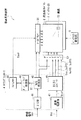
図1は、本発明の一実施の形態に係る液晶表示装置(液晶表示装置1)の全体構成を表すものである。この液晶表示装置1は、液晶表示パネル2と、バックライト部3と、タイミングコントローラ4と、ソースドライバ51およびゲートドライバ52と、バックライト駆動部6とを備えている。
FIG. 1 shows an overall configuration of a liquid crystal display device (liquid crystal display device 1) according to an embodiment of the present invention. The liquid
液晶表示パネル2は、後述するソースドライバ51およびゲートドライバ52から供給される駆動信号によって入力映像信号Dinに基づく映像表示を行うものであり、マトリクス状に並んで配置された複数の画素20を含んで構成されている。また、各画素20内には、後述する画素回路ユニット(図2参照)が形成されている。なお、この画素回路ユニットの詳細構成については、後述する。
The liquid
バックライト部3は、液晶表示パネル2に対して光を照射する光源であり、例えばCCFL(Cold Cathode Fluorescent Lamp:冷陰極蛍光ランプ)やLED(Light Emitting Diode:発光ダイオード)などを含んで構成される。
The
タイミングコントローラ4は、I/O部41と、信号処理部42と、オーバードライブ処理部43と、フレームメモリ44と、基準電源部45と、DC/DCコンバータ46とを有している。このタイミングコントローラ4は、外部からの入力映像信号Din(輝度信号)に対して後述する所定の信号処理を施すことにより、RGB信号である映像信号Doutを生成すると共に、電源電圧Vccの供給に基づいてソースドライバ51およびゲートドライバ52において用いられる電圧を生成するものである。タイミングコントローラ4はまた、ソースドライバ51およびゲートドライバ52の駆動タイミングを制御する役割も果たしている。
The
I/O部41は、入力映像信号Dinを入力して信号処理部42へ供給するものである。信号処理部42は、供給された入力映像信号Dinに対して所定の信号処理を施し、RGB信号である映像信号D1をオーバードライブ処理部43へ供給すると共に、ソースドライバ51およびゲートドライバ52の駆動タイミング制御信号を生成し、ソースドライバ51およびゲートドライバ52へ供給するものである。
The I /
オーバードライブ処理部43は、信号処理部42から供給される現在のフレームの映像信号D1と、後述するフレームメモリ44に記憶されている1つ前の(直前の)フレームの映像信号D2(図示せず)とに基づき、現在のフレームにおいて、後述する通常駆動およびオーバードライブ駆動のうちのどちらによる表示駆動を行うのかを画素20ごとに判定すると共に、この判定結果に基づき、現在のフレームの映像信号D1に対して後述する補正を画素20ごとに行い、そのような補正後の映像信号D2をフレームメモリ44へ書き込む(記憶させる)という処理(詳細は後述)を行うものである。なお、上記したような駆動方法の判定処理および現在のフレームの映像信号D1の補正処理は、例えば図3に示したように、現在のフレームの映像信号D1の階調(例えば、0〜255階調)および過去(1つ前)のフレームの映像信号D2の階調(例えば、0〜255階調)と、補正後の現在のフレームの映像信号の階調とを関連付けてなるルックアップテーブル7を用いてなされるようになっている。なお、このような駆動方法の判定処理および現在のフレームの映像信号D1の補正処理の詳細については、後述する。
The
フレームメモリ44は、上記したように、オーバードライブ処理部43による補正後(処理後)の映像信号を、映像信号D2としてフレーム単位で記憶するものである。
As described above, the
基準電源部45は、電源電圧Vccに基づいて、DC/DCコンバータ46の基準電圧である基準電圧Vrefを生成するものである。DC/DCコンバータ46は、供給される基準電圧Vrefに基づいて所定の直流電圧変換を行うことにより、ソースドライバ51の電源電圧およびゲートドライバ52において用いられる電圧(後述するゲートオン電圧Vonおよび複数種類のゲートオフ電圧Voff1,Voff2,Voff3)をそれぞれ生成し、ソースドライバ51およびゲートドライバ52へ供給するものである。
The reference
ソースドライバ51は、信号処理部42から供給される駆動タイミング制御信号に従って、フレームメモリ44に記憶されている現在のフレームの映像信号D2を映像信号Doutとして入力すると共に、この映像信号Doutに基づく駆動電圧(後述するソース電圧)を液晶表示パネル2の各画素20へ供給するものである。
The
ゲートドライバ52は、信号処理部42から供給される駆動タイミング制御信号に従って、DC/DCコンバータ46からの供給電圧(ゲートオン電圧Vonおよびゲートオフ電圧Voff1,Voff2,Voff3)に基づき、液晶表示パネル2内の各画素20を後述するゲート線に沿って線順次駆動するものである。なお、このゲートドライバ52の詳細構成については、後述する(図4および図5)。
The
バックライト駆動部6は、バックライト部3の点灯動作を制御するものであり、例えばインバータ回路を含んで構成されている。
The
次に図2を参照して、各画素20に形成された画素回路ユニット(液晶表示素子)の構成について詳細に説明する。図2は、画素20内の画素回路ユニットの回路構成例を表したものである。なお、図中の符号m,nはそれぞれ自然数を表しており、画素20(m,n)は、複数の画素20のうちの座標(m,n)に位置する画素を表している。
Next, the configuration of the pixel circuit unit (liquid crystal display element) formed in each
画素20(m,n)には、主容量素子として機能する液晶素子LCと、補助容量素子Csと、TFT素子Q(m,n)とからなる画素回路ユニットが形成されている。また、この画素20(m,n)には、駆動対象の画素回路ユニットを線順次で選択してその画素回路ユニット内のTFT素子Qを前述のゲートオン電圧Vonにより選択的にオン状態にすると共に、このTFT素子Qを前述の複数種類のゲートオフ電圧Voff1,Voff2,Voff3により選択的にオフ状態にするためのゲート線G(n)と、駆動対象の画素回路ユニットに対し、その画素回路ユニット内のTFT素子Qを介して画像データ(映像信号Dout)を供給するソース線S(m)とが接続されている。なお、ゲート線G(n)は、後述するようにゲート線G(n−1)に沿って延在する画素20(m,n−1)等の補助容量線としても機能するようになっている。 In the pixel 20 (m, n), a pixel circuit unit including a liquid crystal element LC functioning as a main capacitive element, an auxiliary capacitive element Cs, and a TFT element Q (m, n) is formed. In the pixel 20 (m, n), the pixel circuit units to be driven are selected in a line sequential manner, and the TFT elements Q in the pixel circuit units are selectively turned on by the gate-on voltage Von. A gate line G (n) for selectively turning off the TFT element Q by the above-described plurality of types of gate-off voltages Voff1, Voff2, and Voff3, and the pixel circuit unit to be driven in the pixel circuit unit. A source line S (m) for supplying image data (video signal Dout) is connected through the TFT element Q. Note that the gate line G (n) also functions as an auxiliary capacitance line such as the pixel 20 (m, n−1) extending along the gate line G (n−1) as described later. Yes.
なお、画素20(m,n)に対してソース線S(m)に沿って線順次動作方向に隣接する画素20(m,n+1)には、図示したようにTFT素子Q(m,n+1)が含まれると共に、ゲート線G(n+1)およびソース線S(m)とが接続され、画素20(m,n)に対してソース線S(m)に沿って線順次動作方向とは逆方向に隣接する画素20(m,n−1)には、図示したように補助容量素子Cs(m,n−1)が含まれると共に、図示しないゲート線G(n−1)およびソース線S(m)が接続されている。また、画素20(m,n)に対してゲート線G(n)に沿って隣接する画素20(m+1,n)には、図示したようにTFT素子Q(m+1,n)および補助容量素子Cs(m+1,n)が含まれると共に、ゲート線G(n)およびソース線S(m+1)が接続されている。さらに、この画素20(m+1,n)に対してソース線S(m+1)に沿って線順次動作方向に隣接する画素20(m+1,n+1)には、図示したようにTFT素子Q(m+1,n+1)が含まれると共に、ゲート線G(n+1)およびソース線S(m+1)とが接続され、画素20(m+1,n)に対してソース線S(m+1)に沿って線順次動作方向とは逆方向に隣接する画素20(m+1,n−1)(図示せず)には、図示したように補助容量素子Cs(m+1,n−1)が含まれると共に、図示しないゲート線G(n−1)およびソース線S(m+1)が接続されている。 The pixel 20 (m, n + 1) adjacent to the pixel 20 (m, n) in the line sequential operation direction along the source line S (m) has a TFT element Q (m, n + 1) as illustrated. And the gate line G (n + 1) and the source line S (m) are connected to the pixel 20 (m, n) along the source line S (m) in the direction opposite to the line sequential operation direction. The pixel 20 (m, n−1) adjacent to the pixel includes the auxiliary capacitance element Cs (m, n−1) as illustrated, and the gate line G (n−1) and the source line S (not illustrated). m) is connected. Further, the pixel 20 (m + 1, n) adjacent to the pixel 20 (m, n) along the gate line G (n) includes a TFT element Q (m + 1, n) and an auxiliary capacitance element Cs as illustrated. (M + 1, n) is included, and the gate line G (n) and the source line S (m + 1) are connected. Further, the pixel 20 (m + 1, n + 1) adjacent to the pixel 20 (m + 1, n) in the line sequential operation direction along the source line S (m + 1) has a TFT element Q (m + 1, n + 1) as illustrated. ) And the gate line G (n + 1) and the source line S (m + 1) are connected to the pixel 20 (m + 1, n) in the direction opposite to the line sequential operation direction along the source line S (m + 1). A pixel 20 (m + 1, n−1) (not shown) adjacent in the direction includes an auxiliary capacitance element Cs (m + 1, n−1) as shown and a gate line G (n−1) not shown. ) And the source line S (m + 1).
液晶素子LCは、ソース線S(m)からTFT素子Q(m,n)を介して一端に供給される映像信号Doutに応じて表示のための動作を行う(表示光を射出する)表示要素として機能しており、図示しない液晶層と、この液晶層を挟む一対の電極とを含んで構成されている。これら一対の電極のうちの一方(一端)側は接続線L1を介してTFT素子Q(m,n)のソースおよび補助容量素子Csの一端に接続され、他方(他端)側はコモン電極VCOMに接続されている。なお、上記液晶層は、例えばTN(Twisted Nematic)モードの液晶などにより構成される。 The liquid crystal element LC performs a display operation (emits display light) in accordance with the video signal Dout supplied to one end from the source line S (m) via the TFT element Q (m, n). And includes a liquid crystal layer (not shown) and a pair of electrodes sandwiching the liquid crystal layer. One (one end) side of the pair of electrodes is connected to the source of the TFT element Q (m, n) and one end of the auxiliary capacitance element Cs via the connection line L1, and the other (other end) side is the common electrode VCOM. It is connected to the. The liquid crystal layer is made of, for example, TN (Twisted Nematic) mode liquid crystal.
補助容量素子Csは、液晶素子LCの蓄積電荷を安定化させるための容量素子であり、一端(一方の電極)が接続線L1を介して液晶素子LCの一端およびTFT素子Q(m,n)のソースに接続されると共に、他端(対向電極)が、ソース線S(m)に沿って線順次動作方向に隣接するゲート線である隣接ゲート線G(n+1)に接続されている。このような構成により各画素20内の画素回路ユニットは、いわゆるCs on gate方式(詳細は後述)の画素回路ユニットとして機能するようになっている。
The auxiliary capacitive element Cs is a capacitive element for stabilizing the stored charge of the liquid crystal element LC, and one end (one electrode) is connected to one end of the liquid crystal element LC and the TFT element Q (m, n) via the connection line L1. The other end (counter electrode) is connected to an adjacent gate line G (n + 1), which is a gate line adjacent to the source line S (m) in the line sequential operation direction. With such a configuration, the pixel circuit unit in each
TFT素子Q(m,n)はMOS−FET(Metal Oxide Semiconductor−Field Effect Transistor)により構成されており、ゲートがゲート線G(n)に接続され、ソースが接続線L1を介して液晶素子LCの一端および補助容量素子Csの一端に接続され、ドレインがソース線S(m)に接続されている。このTFT素子Q(m,n)は、液晶素子LCの一端および補助容量素子Csの一端に対して映像信号Doutを供給するためのスイッチング素子として機能している。具体的には、ゲートドライバ52からゲート線G(n)を介して供給される選択信号(ゲート信号)に応じて、ソース線S(m)と画素20(m,n)内の液晶素子LCおよび補助容量素子Csの一端同士との間を選択的に導通させる(オン状態にする)ようになっている。
The TFT element Q (m, n) is composed of a MOS-FET (Metal Oxide Semiconductor-Field Effect Transistor), the gate is connected to the gate line G (n), and the source is connected to the liquid crystal element LC via the connection line L1. And one end of the auxiliary capacitance element Cs, and the drain is connected to the source line S (m). The TFT element Q (m, n) functions as a switching element for supplying the video signal Dout to one end of the liquid crystal element LC and one end of the auxiliary capacitive element Cs. Specifically, in accordance with a selection signal (gate signal) supplied from the
次に図4および図5を参照して、ゲートドライバ52の回路構成の詳細について説明する。このゲートドライバ52は、図4に示したシフトレジスタ部521と、図5に示した出力部522とを含んで構成されている。
Next, the circuit configuration of the
シフトレジスタ部521は、信号処理部42から供給される駆動タイミング制御信号であるストローブ信号STVおよびパルス信号(クロック信号)CPVに基づいて、後述するような順次異なるタイミングで「H」状態となるストローブ信号STV1,STV2,STV3,STV4,…を生成するものであり、複数のフリップフロップ回路(例えば、図4に示したフリップフロップ回路FF1〜FF5,…)を含んで構成されている。フリップフロップ回路FF1のデータ入力端子Dにはストローブ信号STVが供給されると共に、各フリップフロップ回路FF1〜FF5,…のクロック端子CKにはパルス信号CPVが互いに並列に供給されるようになっている。また、フリップフロップ回路FF1のデータ出力端子Qからはストローブ信号STV1が出力されると共にこのストローブ信号STV1はフリップフロップ回路FF2のデータ入力端子Dに供給され、フリップフロップ回路FF2のデータ出力端子Qからはストローブ信号STV2が出力されると共にこのストローブ信号STV2はフリップフロップ回路FF3のデータ入力端子Dに供給され、フリップフロップ回路FF3のデータ出力端子Qからはストローブ信号STV3が出力されると共にこのストローブ信号STV3はフリップフロップ回路FF4のデータ入力端子Dに供給され、フリップフロップ回路FF4のデータ出力端子Qからはストローブ信号STV4が出力されると共にこのストローブ信号STV4はフリップフロップ回路FF5のデータ入力端子Dに供給されるようになっている。
Based on the strobe signal STV and the pulse signal (clock signal) CPV, which are drive timing control signals supplied from the
出力部522は、シフトレジスタ部521から供給されるストローブ信号STV1,STV2,STV3,STV4,…およびDC/DCコンバータ46から供給されるゲートオン電圧Vonおよびゲートオフ電圧Voff1,Voff2,Voff3に基づいて、ゲートドライバ52の出力信号であるゲート信号(ゲート電圧VG(1),VG(2),…)を生成するものであり、各ゲート電圧ごとに、4つのアナログスイッチ部(例えば、図5に示したように、ゲート電圧VG(1)に対するアナログスイッチ部SW1〜SW4)と、1つのフリップフロップ回路(例えば、図5に示したように、ゲート電圧VG(1)に対するフリップフロップ回路FF0)とを含んで構成されている。ここで、ゲート電圧VG(1)に対するアナログスイッチSW1〜SW4およびフリップフロップ回路FF0について代表して説明すると、アナログスイッチSW1は、ストローブ信号STV1の値に応じてゲートオン電圧Vonおよびゲートオフ電圧Voff1のうちの一方を選択出力するもの(具体的には、ストローブ信号STV1=「H」のときにはゲートオン電圧Vonを選択出力する一方、ストローブ信号STV1=「L」のときにはゲートオフ電圧Voff1を選択出力する)である。また、アナログスイッチSW2は、ストローブ信号STV2の値に応じてゲートオフ電圧Voff2およびアナログスイッチSW1からの出力電圧のうちの一方を選択出力するもの(具体的には、ストローブ信号STV2=「H」のときにはゲートオフ電圧Voff2を選択出力する一方、ストローブ信号STV2=「L」のときにはアナログスイッチSW1からの出力電圧を選択出力する)である。また、アナログスイッチSW3は、ストローブ信号STV2の値に応じてゲートオフ電圧Voff3およびアナログスイッチSW1からの出力電圧のうちの一方を選択出力するもの(具体的には、ストローブ信号STV2=「H」のときにはゲートオフ電圧Voff3を選択出力する一方、ストローブ信号STV2=「L」のときにはアナログスイッチSW1からの出力電圧を選択出力する)である。また、フリップフロップ回路FF0は、ストローブ信号STV1をクロック端子CKに入力すると共に反転データ出力端子Q−からの出力データをデータ入力端子DおよびアナログスイッチSW4の選択端子に供給しており、「H」状態と「L」状態とが交互に発生するトグル信号生成部として機能している。また、アナログスイッチSW4は、フリップフロップ回路FF0から供給される上記トグル信号の値に応じてアナログスイッチSW2からの出力電圧およびアナログスイッチSW3からの出力電圧のうちの一方を選択し(具体的には、トグル信号=「H」のときにはアナログスイッチSW2からの出力電圧を選択する一方、トグル信号=「L」のときにはアナログスイッチSW3からの出力電圧を選択する)、ゲート電圧VG(1)として出力するものである。
The output unit 522 generates a gate based on the strobe signals STV1, STV2, STV3, STV4,... Supplied from the
ここで、タイミングコントローラ4、ソースドライバ51およびゲートドライバ52が本発明における「駆動手段」および「液晶駆動回路」の一具体例に対応し、オーバードライブ処理部43が本発明における「判定手段」および「補正手段」の一具体例に対応する。
Here, the
次に、このような構成からなる本実施の形態の液晶表示装置1の動作について、詳細に説明する。
Next, the operation of the liquid
まず、図1,図2および図4〜図6を参照して、液晶表示装置1の全体動作について説明する。ここで図6は、ゲートドライバ52の動作をタイミング波形図で表したものであり、(A)はパルス信号(クロック信号)CPVの電圧波形を、(B)〜(F)はそれぞれストローブ信号STV,STV1〜STV4の電圧波形を、(G)〜(I)はそれぞれゲート信号G(1)〜G(3)の電圧を示すゲート電圧VG(1)〜VG(3)の電圧波形を、それぞれ表している。
First, the overall operation of the liquid
この液晶表示装置1では、図1に示したように、タイミングコントローラ4において、外部からの入力映像信号Dinに対して所定の信号処理が施され、RGB信号である映像信号Doutが生成されると共に、電源電圧Vccの供給に基づいてソースドライバ51およびゲートドライバ52において用いられる電圧が生成される。
In the liquid
具体的には、まず、I/O部41を介して入力した入力映像信号Dinが、信号処理部42によって所定の信号処理が施され、RGB信号である映像信号D1が生成されると共に、この信号処理部42においてソースドライバ51およびゲートドライバ52の駆動タイミング制御信号が生成され、ソースドライバ51およびゲートドライバ52へ供給される。
Specifically, first, the input video signal Din input through the I /
次に、オーバードライブ処理部43では、信号処理部42から供給される現在のフレームの映像信号D1と、フレームメモリ44に記憶されている1つ前の(直前の)フレームの映像信号D2とに基づき、後述する駆動方法の判定処理および現在のフレームの映像信号D1の補正処理が画素20ごとになされ、これにより補正後の映像信号D2がフレームメモリ44へ書き込まれる。
Next, in the
一方、基準電源部45により供給される基準電圧Vrefに基づいてDC/DCコンバータ46により直流電圧変換がなされ、生成されたソースドライバ51の電源電圧がソースドライバ51へ供給されると共に、生成されたゲートオン電圧Vonおよび3つのゲートオフ電圧Voff1,Voff2,Voff3がそれぞれ、ゲートドライバ52へ供給される。
On the other hand, DC voltage conversion is performed by the DC /
ここで、ゲートドライバ52では、信号処理部42により供給される駆動タイミング制御信号(具体的には、ストローブ信号STVおよびパルス信号(クロック信号)CPV)、ならびにDC/DCコンバータ46により供給されるゲートオン電圧Vonおよびゲートオフ電圧Voff1,Voff2,Voff3に基づき、例えば図6に示したようにして、各ゲート線に供給されるゲート電圧が生成される。
Here, in the
具体的には、まず、図4に示したシフトレジスタ部521では、信号処理部42により供給されるストローブ信号STV(図6(A))およびパルス信号CPV(図6(B))に基づき、図6(C)〜(F)にそれぞれ示したようなタイミング波形(タイミングt0〜t5)からなるストローブ信号STV1〜STV4等が生成される。
Specifically, first, in the
次に、図5に示した出力部522では、シフトレジスタ部521から供給されるストローブ信号STV1,STV2,STV3,STV4,…およびDC/DCコンバータ46から供給されるゲートオン電圧Vonおよびゲートオフ電圧Voff1,Voff2,Voff3に基づいて、例えば図6(G)〜(I)にそれぞれ示したようなタイミング波形(タイミングt1〜t5)からなるゲート電圧VG(1),VG(2),VG(3),…が生成される。すなわち、ゲートオン電圧Vonおよびゲートオフ電圧Voff1,Voff2,Voff3の4値を用いた線順次のゲート電圧が生成される(4値駆動のゲート電圧となる)。これにより、液晶表示パネル2内の各画素20がゲート線に沿って線順次により4値駆動される。
Next, in the output unit 522 shown in FIG. 5, the strobe signals STV1, STV2, STV3, STV4,... Supplied from the
一方、ソースドライバ51では、信号処理部42から供給される駆動タイミング制御信号に従って、フレームメモリ44に記憶されている現在のフレームの映像信号D2を映像信号Doutとして入力すると共に、この映像信号Doutに基づく駆動電圧(ソース電圧)が生成され、ソース線に沿って液晶表示パネル2の各画素20へ供給される。
On the other hand, in the
ここで、ゲートドライバ52およびソースドライバ51から出力される各画素20内への駆動電圧(ゲート電圧およびソース電圧)によって、各画素20に対する線順次表示駆動動作がなされる。具体的には、図2に示した画素20(m,n)内の画素回路ユニットでは、以下のようにしていわゆるライン反転駆動動作がなされる。
Here, the line sequential display drive operation for each
まず、ソースドライバ51からソース線S(m)を介して画素20(m,n)用の映像信号Doutが供給されると共に、ゲートドライバ52からゲート線G(n)を介して画素20(m,n)用の選択信号(具体的には、ゲート電圧VG(n)におけるゲートオン電圧Von)が供給されると、ゲート線G(n)にパルス状の電位(ゲートオン電圧Vonの電位)が発生する。これにより、TFT素子Q(m,n)がオン状態となり、接続線L1を介して映像信号Doutに基づく電流が流れ、液晶素子LCおよび補助容量素子Csの一端同士に電荷が蓄積される(画像データが供給される)。すなわち、映像信号Doutに基づく電圧が、画素20(m,n)内の液晶素子LCおよび補助容量素子Cs(m,n)の両端間にそれぞれ印加される。
First, the video signal Dout for the pixel 20 (m, n) is supplied from the
次に、ゲート線G(n)により供給されるゲートオフ電圧Voff2またはゲートオフ電圧Voff3(図6(G),(I)に示したように、正極のときにはゲートオフ電圧Voff2、負極のときにはゲートオフ電圧Voff3)によってTFT素子Q(m,n)が選択的にオフ状態となると、ソース線S(m)からの映像信号Doutの供給が停止され、画素20(m,n)内の液晶素子LCおよび補助容量素子Cs(m,n)の両端間の電圧が保持される。 Next, the gate-off voltage Voff2 or the gate-off voltage Voff3 supplied by the gate line G (n) (as shown in FIGS. 6 (G) and (I), the gate-off voltage Voff2 is positive, and the gate-off voltage Voff3 is negative). When the TFT element Q (m, n) is selectively turned off by this, the supply of the video signal Dout from the source line S (m) is stopped, and the liquid crystal element LC and the auxiliary capacitor in the pixel 20 (m, n) are stopped. The voltage across the element Cs (m, n) is held.
次に、ソース線S(m)に沿って線順次動作方向に隣接するゲート線である隣接ゲート線G(n+1)によって補助容量素子Cs(m,n)の他端(対向電極)に、例えば図6(G)〜(I)中の矢印P21〜P23に示したように、ゲートオフ電圧Voff2の電位からゲートオフ電圧Voff1の電位への変動や、ゲートオフ電圧Voff3の電位からゲートオフ電圧Voff1の電位への変動のように、ゲートオフ電圧の電位が時間変化しつつ供給されると、それに伴って補助容量素子Cs(m,n)および液晶素子LCの両端間の電圧も、上記した映像信号Doutに基づく電圧から変化する(いわゆるCs on gate方式による作用)。 Next, the other end (counter electrode) of the auxiliary capacitive element Cs (m, n) is formed by the adjacent gate line G (n + 1) which is a gate line adjacent to the source line S (m) in the line sequential operation direction, As indicated by arrows P21 to P23 in FIGS. 6G to 6I, a change from the potential of the gate-off voltage Voff2 to the potential of the gate-off voltage Voff1, or from the potential of the gate-off voltage Voff3 to the potential of the gate-off voltage Voff1. as a variation, the potential of the gate-off voltage is supplied changing time, the auxiliary capacitor element Cs (m, n) with it and also the voltage across the liquid crystal element LC, based on the image signal Dout that describes above It changes from the voltage (action by the so-called Cs on gate method).
以上のような液晶表示パネル2における線順次表示駆動動作により、バックライト駆動部6の駆動動作によりバックライト部3から照射される照明光が、液晶表示パネル2により画素20ごとに変調され、表示光として液晶表示パネル2から出力される。これにより、入力映像信号Dinに基づく表示光により、映像表示がなされる。
By the line sequential display driving operation in the liquid
次に、図1,図2,図4〜図6に加えて図3,図7〜図11を参照して、本発明の特徴的部分の1つである、オーバードライブ処理部43による駆動方法の判定処理および現在のフレームの映像信号D1の補正処理の詳細について詳細に説明する。ここで、図7は、このようなオーバードライブ処理部43による処理の一例を流れ図で表したものである。また、図8は、映像信号D1(オーバードライブ処理部43への入力データ)および映像信号D2(フレームメモリ44への書き込みデータ)のフレーム単位での時間変化とオーバードライブ処理部43による処理との関係をタイミング図で表したものであり、図中の3×3のマス目の左上に示した各数字は、ある画素20における画素データ(映像信号の輝度の階調レベル(0〜255階調))を示している。また、図9は、白表示の際における映像信号Doutの各画素20への書き込み時および最終安定時の液晶素子LCの両端間に印加される電圧波形を、図10は、黒表示の際における映像信号Doutの各画素20への書き込み時および最終安定時の液晶素子LCの両端間に印加される電圧波形を、それぞれ表している。また、図11は、オーバードライブ駆動時における液晶素子LCの両端間に印加される電圧波形をタイミング図で表したものであり、図11(A)は黒表示状態から白表示状態への遷移の際のオーバードライブ駆動を、図11(B)は白表示状態から黒表示状態への遷移の際のオーバードライブ駆動を、それぞれ表している。
Next, referring to FIGS. 3, 7 to 11 in addition to FIGS. 1, 2, 4 to 6, a driving method by the
まず、オーバードライブ処理部43は、信号処理部42から現在のフレームの映像信号D1を取得すると(図7のステップS101)、例えば図3に示したルックアップテーブル7を参照することにより、取得した現在のフレームの映像信号D1と、フレームメモリ44に書き込まれている(記憶されている)直前のフレームにおける補正後の映像信号D2とを比較し(ステップS102)、これら映像信号D1,D2における輝度レベル差(輝度の階調レベルの差)がオーバードライブ処理を施すべき程度に大きいか否か(ルックアップテーブル7により規定されている閾値よりも大きいか否か)を判断する(ステップS103)。
First, when the
具体的には、例えば図8に示したように、まず、図8(A)に示した直前の映像信号D2と図8(B)に示した現在の映像信号D1とを比較すると(ステップS103)、映像信号D1,D2における輝度の階調レベル差が閾値よりも小さいため(ステップS103:N)、この画素においては通常駆動による表示駆動を行うべきであると判定し、現在のフレームの映像信号D1における輝度の階調レベルを下にシフト(下げる)する補正である通常処理を行う(ステップS104、図8(B)、図10中の矢印P51)。したがって、フレームメモリ44には、図8(B)に示したように、「−20」という階調レベルのデータが、現在のフレームにおける補正後の映像信号D2として書き込まれる(ステップS108)。また、この際、前述したCs on gate方式の作用により、補助容量素子Cs(m,n)および液晶素子LCの両端間の電圧がその後この映像信号D2(Dout)に基づく電圧から変化して安定状態となったとき(最終安定時)、例えば図10に示したように、通常駆動(正極)によって、補正後の映像信号D2に基づく輝度レベルが、補正前の映像信号D1に基づく本来の輝度レベル(例えば、図中の黒レベル(正極))と同等のものとなっており、これにより補正の前後で輝度レベルが変化しないようになっている。
Specifically, as shown in FIG. 8, for example, the immediately preceding video signal D2 shown in FIG. 8A is compared with the current video signal D1 shown in FIG. 8B (step S103). ) Since the difference in luminance gradation level in the video signals D1 and D2 is smaller than the threshold value (step S103: N), it is determined that display driving by normal driving should be performed in this pixel, and the video of the current frame Normal processing, which is correction for shifting (decreasing) the luminance gradation level in the signal D1, is performed (step S104, FIG. 8B, arrow P51 in FIG. 10). Therefore, as shown in FIG. 8B, the data of the gradation level “−20” is written in the
なお、その後はオーバードライブ処理部43による処理全体を終了するか否かが判断され(ステップS109)、終了しないと判断した場合には(ステップS109:N)、ステップS101へと戻ることとなる。
After that, it is determined whether or not the entire process by the
次に、上記と同様のステップS101,S102の後に、図8(B)に示した直前の映像信号D2と図8(C)に示した現在の映像信号D1とを比較すると(ステップS103)、映像信号D1,D2における輝度の階調レベル差が閾値よりも大きいため(ステップS103:Y)、この画素においてはオーバードライブ駆動による表示駆動を行うべきであると判定し、次にオーバードライブ処理部43は、直前のフレームから現在のフレームへの遷移が黒表示状態から白表示状態への遷移か否かを判断する(ステップS105)。ここでは、図8(B),(C)に示したように黒表示状態から白表示状態への遷移であるため(ステップS105:Y)、オーバードライブ処理部43は、現在のフレームの映像信号D1における輝度の階調レベルを変化させずに(輝度の階調レベルをシフトさせずに)そのまま用いるというオーバードライブ処理を行う(ステップS106、図8(C))。したがって、フレームメモリ44には、図8(C)に示したように、そのまま「255」という階調レベルのデータが現在のフレームにおける補正後の映像信号D2として書き込まれる(ステップS108)。したがって、例えば図9に示したオーバードライブ駆動(正極)によって、Cs on gate方式の作用を用いたオーバードライブ駆動がなされ、これにより例えば図11(A)中の矢印P61で示したように、直前のフレームと現在のフレームとの間での液晶素子LCの両端間の電圧変化が、現在のフレームの映像信号D1(補正前の画像データ)に基づく本来の電圧変化よりも大きくなり、図中の矢印P62で示したように、黒表示状態から白表示状態への遷移の際の液晶の応答速度が改善する。
Next, after the same steps S101 and S102 as described above, the immediately preceding video signal D2 shown in FIG. 8B is compared with the current video signal D1 shown in FIG. 8C (step S103). Since the difference in luminance gradation level in the video signals D1 and D2 is larger than the threshold (step S103: Y), it is determined that display drive by overdrive driving should be performed for this pixel, and then the
次に、上記と同様のステップS109,S101,S102の後に、図8(C)に示した直前の映像信号D2と図8(D)に示した現在の映像信号D1とを比較すると(ステップS103)、映像信号D1,D2における輝度の階調レベル差が閾値よりも小さいため(ステップS103:N)、この画素においては通常駆動による表示駆動を行うべきであると判定し、現在のフレームの映像信号D1における輝度の階調レベルを下にシフト(下げる)する補正である通常処理を行う(ステップS104、図8(D)、図9中の矢印P31)。したがって、フレームメモリ44には、図8(D)に示したように、「230」という階調レベルのデータが、現在のフレームにおける補正後の映像信号D2として書き込まれ(ステップS108)、例えば図9に示したように通常駆動(正極)によって、Cs on gate方式の作用を用いた通常駆動がなされる。
Next, after steps S109, S101, and S102 similar to the above, the immediately preceding video signal D2 shown in FIG. 8C is compared with the current video signal D1 shown in FIG. 8D (step S103). ) Since the difference in luminance gradation level in the video signals D1 and D2 is smaller than the threshold value (step S103: N), it is determined that display driving by normal driving should be performed in this pixel, and the video of the current frame Normal processing, which is correction for shifting (decreasing) the luminance gradation level in the signal D1, is performed (step S104, FIG. 8D, arrow P31 in FIG. 9). Therefore, as shown in FIG. 8D, data of the gradation level “230” is written in the
次に、上記と同様のステップS109,S101,S102の後に、図8(D)に示した直前の映像信号D2と図8(E)に示した現在の映像信号D1とを比較すると(ステップS103)、映像信号D1,D2における輝度の階調レベル差が閾値よりも大きいため(ステップS103:Y)、この画素においてはオーバードライブ駆動による表示駆動を行うべきであると判定し、次に前述したように、直前のフレームから現在のフレームへの遷移が黒表示状態から白表示状態への遷移か否かを判断する(ステップS105)。ここでは、図8(D),(E)に示したように白表示状態から黒表示状態への遷移であるため(ステップS105:N)、オーバードライブ処理部43は、現在のフレームの映像信号D1における輝度の階調レベルを、通常駆動の際の補正(図10中の矢印P51)よりも過剰に下がるようにする補正であるオーバードライブ処理を行う(ステップS107、図8(E)、図10中の矢印P53)。したがって、フレームメモリ44には、図8(E)に示したように、「80」という階調レベルのデータが、現在のフレームにおける補正後の映像信号D2として書き込まれ(ステップS108)、例えば図10に示したオーバードライブ駆動(正極)によって、Cs on gate方式の作用を用いたオーバードライブ駆動がなされ、これにより例えば図11(B)中の矢印P71で示したように、直前のフレームと現在のフレームとの間での液晶素子LCの両端間の電圧変化が、現在のフレームの映像信号D1(補正前の画像データ)に基づく本来の電圧変化よりも大きくなり、図中の矢印P72で示したように、白表示状態から黒表示状態への遷移の際の液晶の応答速度が改善する。
Next, after steps S109, S101, and S102 similar to the above, the immediately preceding video signal D2 shown in FIG. 8D is compared with the current video signal D1 shown in FIG. 8E (step S103). ) Since the difference between the gradation levels of the luminance in the video signals D1 and D2 is larger than the threshold value (step S103: Y), it is determined that display drive by overdrive driving should be performed on this pixel. As described above, it is determined whether or not the transition from the previous frame to the current frame is a transition from the black display state to the white display state (step S105). Here, since the transition from the white display state to the black display state is performed as shown in FIGS. 8D and 8E (step S105: N), the
なお、図9に示した白表示の際の通常駆動(負極)およびオーバードライブ駆動(負極)については、図9中の矢印P41,P42,P43に示したように、上記した白表示の際の通常駆動(正極)およびオーバードライブ駆動(正極)の場合と同様の動作となるため、説明を省略する。また、図示しない黒表示の際の通常駆動(負極)およびオーバードライブ駆動(負極)についても、上記した黒表示の際の通常駆動(正極)およびオーバードライブ駆動(正極)の場合と同様の動作となるため、説明を省略する。 Note that the normal drive (negative electrode) and overdrive drive (negative electrode) in white display shown in FIG. 9 are as shown in arrows P41, P42, and P43 in FIG. Since the operation is the same as in the case of normal driving (positive electrode) and overdrive driving (positive electrode), the description is omitted. In addition, normal driving (negative electrode) and overdrive driving (negative electrode) during black display (not shown) are the same operations as in the above-described normal driving (positive electrode) and overdrive driving (positive electrode) during black display. Therefore, the description is omitted.
このようにして本実施の形態の液晶表示装置1では、ゲート線Gにより供給されるゲートオン電圧Vonによって駆動対象の画素20内のTFT素子Qが選択的にオン状態となると、ソース線SからこのTFT素子Qを介して映像信号Doutが供給され、この映像信号Doutに基づく電圧が、画素20内の液晶素子LCおよび補助容量素子Csの両端間にそれぞれ印加される。その後、ゲート線Gにより供給される複数種類のゲートオフ電圧Voff1,Voff2,Voff3のうちの一のゲートオフ電圧(Voff2またはVoff3)によってTFT素子Qが選択的にオフ状態となると、ソース線Sからの映像信号Doutの供給が停止され、液晶素子LCおよび補助容量素子Csの両端間の電圧が保持される。そしてその後にソース線Sに沿って線順次動作方向に隣接するゲート線である隣接ゲート線によって補助容量素子Csの他端(対向電極)に、複数種類のゲートオフ電圧の電位が時間変化しつつ供給されると、この補助容量素子Csおよび液晶素子Lcの両端間の電圧が、映像信号Doutに基づく電圧から変化する。
As described above, in the liquid
ここで、通常駆動の際には、現在のフレームの映像信号D1がその輝度レベルが所定の階調分だけ下がるように補正された後の映像信号D2を基に表示駆動がなされるため、このような補正後の映像信号D2に基づき、上記のように補助容量素子Csおよび液晶素子LCの両端間の電圧が変化した後に、これらの両端間にそれぞれ、補正前の映像信号D1に基づく本来の電圧値が印加されるように(オーバードライブ駆動がなされないように、つまり通常駆動がなされるように)調整可能となる。また、オーバードライブ駆動の際には、液晶素子LCの両端間の電圧変化が現在のフレームの映像信号D1に基づく本来の電圧変化よりも大きくなるような映像信号(補正後の映像信号D2)を基に表示駆動がなされるため、上記のように補助容量素子Csおよび液晶素子LCの両端間の電圧が変化した後に、これらの両端間にそれぞれ、補正前の映像信号D1に基づく本来の電圧値よりも大きな電圧値が印加され、これにより本来の電圧変化よりも大きくなるような表示駆動、すなわちオーバードライブ駆動がなされる。したがって、このような構成および作用により、本実施の形態では、駆動素子であるTFT素子Qの耐圧を上げることなく、液晶の応答速度を向上させることが可能となる。 Here, in normal driving, display driving is performed based on the video signal D2 after the video signal D1 of the current frame is corrected so that the luminance level thereof is lowered by a predetermined gradation. After the voltage between both ends of the auxiliary capacitive element Cs and the liquid crystal element LC changes as described above based on the corrected video signal D2, the original voltage based on the video signal D1 before correction is respectively applied between both ends. Adjustment is possible so that a voltage value is applied (so that overdrive driving is not performed, that is, normal driving is performed). In overdrive driving, a video signal (corrected video signal D2) in which the voltage change across the liquid crystal element LC is larger than the original voltage change based on the video signal D1 of the current frame is generated. Since the display drive is performed based on the above, after the voltage between the both ends of the auxiliary capacitance element Cs and the liquid crystal element LC changes as described above, the original voltage value based on the video signal D1 before correction is respectively applied between the both ends. large deal of voltage value is applied, thereby the original larger such display drive than the voltage change, i.e. the overdrive driving is performed than. Therefore, with this configuration and action, in this embodiment, the response speed of the liquid crystal can be improved without increasing the withstand voltage of the TFT element Q that is a driving element.
具体的には、オーバードライブ処理部43が、現在のフレームの映像信号D1とその直前のフレームの映像信号D2とに基づき、現在のフレームにおいて、通常駆動およびオーバードライブ駆動のうちのどちらによる表示駆動を行うのかを画素20ごとに判定すると共に、そのような判定結果に基づき、現在の単位フレームの映像信号D1を画素20ごとに補正するようにしたので、上記の効果を得ることができる。また、判定の際には、現在のフレームとその直前のフレームとの間の映像信号の輝度レベル差が所定の閾値以上の画素20に対し、オーバードライブ駆動による表示駆動を行うと判定する一方、輝度レベル差が閾値未満の画素に対し、通常駆動による表示駆動を行うと判定するようにしたので、上記の効果を得ることができる。
Specifically, the
また、補正の際には、上記輝度レベル差が閾値以上の画素において、その輝度レベル差が大きくなるのに応じて液晶素子LCの両端間の電圧変化がより大きくなるように、現在のフレームの映像信号D1の補正を行うようにしたので、液晶の応答速度の改善の必要性に応じてオーバードライブ量の調整をすることができる。 Further, at the time of correction, in the pixel having the luminance level difference equal to or larger than the threshold value, the current frame is changed so that the voltage change between both ends of the liquid crystal element LC becomes larger as the luminance level difference becomes larger. Since the video signal D1 is corrected, the overdrive amount can be adjusted according to the necessity of improving the response speed of the liquid crystal.
また、オーバードライブ駆動の際に、黒表示状態から白表示状態へ遷移する画素においては、現在のフレームの映像信号D1をその輝度レベルを変化させずにそのまま用いて表示駆動を行うようにしたので、補助容量素子Csおよび液晶素子LCの両端間の電圧が変化した後にこれらの両端間にそれぞれ、補正前の映像信号D1に基づく白表示状態の本来の電圧値よりも大きくな電圧値が印加されるため、これにより黒表示状態から白表示状態への遷移の際の本来の電圧変化よりも大きくなるような表示駆動、すなわち黒表示状態から白表示状態への遷移の際のオーバードライブ駆動を行うことが可能となる。 In addition, in overdrive driving, in the pixels that transition from the black display state to the white display state, display drive is performed using the video signal D1 of the current frame as it is without changing the luminance level. After the voltage between the both ends of the auxiliary capacitance element Cs and the liquid crystal element LC changes, a voltage value larger than the original voltage value in the white display state based on the video signal D1 before correction is applied between these both ends. For this reason, display driving is performed such that the change in voltage is larger than the original voltage change at the time of transition from the black display state to the white display state, that is, overdrive drive at the time of transition from the black display state to the white display state. It becomes possible.
また、オーバードライブ駆動の際に、白表示状態から黒表示状態へ遷移する画素においては、現在のフレームの映像信号D1が通常駆動の際の補正よりも輝度レベルが過剰に下がるように補正された後の映像信号D2を基に表示駆動を行うようにしたので、補助容量素子Csおよび液晶素子LCの両端間の電圧が変化した後にこれらの両端間にそれぞれ、補正前の映像信号D1に基づく黒表示状態の本来の電圧値よりも小さな電圧値が印加されるため、これにより白表示状態から黒表示状態への遷移の際の本来の電圧変化よりも大きくなるような表示駆動、すなわち白表示状態から黒表示状態への遷移の際のオーバードライブ駆動を行うことが可能となる。 In addition, at the time of overdrive driving, in the pixel transitioning from the white display state to the black display state, the video signal D1 of the current frame is corrected so as to be excessively lower than the correction at the time of normal driving. Since the display drive is performed based on the subsequent video signal D2, after the voltage between both ends of the auxiliary capacitance element Cs and the liquid crystal element LC changes, the black signal based on the uncorrected video signal D1 is applied between both ends. Since a voltage value smaller than the original voltage value in the display state is applied, this causes display drive that is larger than the original voltage change at the transition from the white display state to the black display state, that is, the white display state It becomes possible to perform overdrive driving at the time of transition from the state to the black display state.
さらに、通常駆動の際において、液晶素子LCの両端間の電圧が安定状態となったときに、補正後の映像信号D2に基づく輝度レベルが補正前の映像信号D1に基づく輝度レベルと同等となっているようにしたので、補助容量素子Csおよび液晶素子LCの両端間の電圧が変化して液晶素子LCの両端間の電圧が安定状態となったときに、補正前の映像信号D1に基づく輝度レベルと同等の輝度レベルとなっているため、通常駆動の際の輝度レベルが変化しないように(すなわち、表示輝度の変動を伴わないように)調整しつつ、オーバードライブ駆動を行うことが可能となる。 Furthermore, when the voltage across the liquid crystal element LC becomes stable during normal driving, the luminance level based on the corrected video signal D2 is equivalent to the luminance level based on the video signal D1 before correction. Therefore, when the voltage across the auxiliary capacitive element Cs and the liquid crystal element LC changes and the voltage across the liquid crystal element LC becomes stable, the luminance based on the video signal D1 before correction Since the brightness level is equivalent to the level, overdrive driving can be performed while adjusting the brightness level so that it does not change during normal driving (that is, without changing display brightness). Become.
以上、実施の形態を挙げて本発明を説明したが、本発明はこの実施の形態に限定されるものではなく、種々の変形が可能である。 While the present invention has been described with reference to the embodiment, the present invention is not limited to this embodiment, and various modifications can be made.
例えば、上記実施の形態では、液晶表示パネル2内の各画素回路ユニットをいわゆるライン反転により表示駆動する場合について説明したが、例えば、いわゆるフレーム反転やドット反転により表示駆動するようにしてもよい。具体的には、ドット反転により表示駆動する場合には、例えば図12に示した液晶表示パネル2Aを備えた液晶表示装置1Aのように、上記実施の形態のゲートドライバ52に対応する2つのゲートドライバ52A,52Bを設けると共に、この液晶表示パネル2A内の各画素21において、例えば図13に示したように、隣接する画素21間で交互に2つのゲート線Ga(ゲートドライバ52Aに接続されたもの),Gb(ゲートドライバ52Bに接続されたもの)がTFT素子Qおよび補助容量素子Csに接続されると共に、これらゲート線Ga,Gbに沿って隣接する画素21同士およびソース線Sに沿って隣接する画素21同士でそれぞれ互いに逆極性の電圧が液晶素子LCの両端間に印加されるように(ドット反転となるように)表示駆動を行うようにすればよい。
For example, in the above embodiment, the case where each pixel circuit unit in the liquid
さらに、上記実施の形態では、DC/DCコンバータ46により3種類のゲートオフ電圧Voff1,Voff2,Voff3を生成すると共にこれら3種類のゲートオフ電圧Voff1,Voff2,Voff3を用いてゲートドライバ52がゲート電圧を生成する場合(4値駆動)について説明したが、ゲートオフ電圧の種類の数についてはこれには限られず、例えば4種類以上のゲートオフ電圧を用いるようにしてもよい。
Furthermore, in the above embodiment, the three types of gate off voltages Voff1, Voff2, and Voff3 are generated by the DC /
1,1A…液晶表示装置、2,2A…液晶表示パネル、20,20(m,n),20(m+1,n),20(m,n−1),20(m,n+1),20(m+1,n+1),21,21(m,n),21(m+1,n),21(m,n−1),21(m,n+1),21(m+1,n+1)…画素、3…バックライト部、4…タイミングコントローラ、41…I/O部、42…信号処理部、43…オーバードライブ処理部、44…フレームメモリ、45…基準電源部、46…DC/DCコンバータ、51…ソースドライバ、511…D/A変換部、512…演算部、513…電源部、514…補助容量電圧生成部、52,52A,52B…ゲートドライバ、521…シフトレジスタ部、522…出力部、6…バックライト駆動部、7…ルックアップテーブル(LUT)、Din…入力映像信号、D1…信号処理後の映像信号、D2…補正後(処理後)の映像信号、Dout…ソースドライバへ供給される出力映像信号、Vcc…電源電圧、Vref…基準電圧、Von…ゲートオン電圧、Voff1,Voff2,Voff3…ゲートオフ電圧、LC…液晶素子、Cs…補助容量素子、Q1…TFT素子、L1…接続線、G(n),G(n+1),Ga(n),Ga(n+1),Gb(n),Gb(n+1)…ゲート線(補助容量線)、S(m),S(m+1)…ソース線、VCOM…コモン電極、FF0〜FF5…フリップフロップ回路、SW1〜SW4…アナログスイッチ部、CPV…パルス信号(クロック信号)、STV,STV1〜STV4…ストローブ信号、VG(1)〜VG(3)…ゲート電圧、t0〜t5…タイミング。
DESCRIPTION OF
Claims (3)
駆動対象の画素を線順次で選択し、選択した画素のTFT素子を所定のオン電圧により選択的にオン状態にすると共に、前記TFT素子を所定のオフ電圧により選択的にオフ状態にするための複数のゲート線と、
駆動対象の画素に対し、前記TFT素子を介して画像データを供給するための複数のソース線と、
各ゲート線の隣接ゲート線における前記オフ電圧を、前記画像データの輝度レベルに依存せずに一律に時間変化させつつ線順次動作を行うことにより、前記画素の表示駆動を行う駆動手段と
を備え、
前記液晶素子は、その一端が前記TFT素子の一端に接続され、
前記補助容量素子は、その一端が前記TFT素子の一端に接続されると共に、他端が前記隣接ゲート線に接続され、
前記駆動手段は、
現在の単位フレームの画像データとその直前の単位フレームの画像データとに基づいて、それらの画像データの輝度レベル差が所定の閾値未満の画素に対し、現在の単位フレームにおいて通常駆動による表示駆動を行うと判定する一方、前記輝度レベル差が前記閾値以上の画素に対し、現在の単位フレームにおいてオーバードライブ駆動による表示駆動を行うと判定する判定手段と、
前記通常駆動による表示駆動を行うと判定された画素については、現在の単位フレームの画像データを、その輝度レベルが所定の分だけ下がるように補正する一方、前記オーバードライブ駆動による表示駆動を行うと判定された画素については、現在の単位フレームの画像データを、その直前の単位フレームと現在の単位フレームとの間での前記液晶素子の両端間電圧の変化が増加すると共に前記輝度レベル差が大きくなるのに応じて前記両端間電圧の変化がより大きくなるような画像データに補正する補正手段と、
前記補正手段による補正後の画像データを基に、前記表示駆動を画素ごと実施する駆動ドライバと
を有し、
前記補正手段は、
前記通常駆動による表示駆動を行うと判定された画素については、補正後の画像データに基づいて前記液晶素子の両端間に電圧を印加しこれが安定した後の状態における輝度レベルが、補正前の画像データに基づいて前記液晶素子の両端間に電圧を印加した直後における輝度レベルと同等となるように、現在の単位フレームの画像データを補正し、
前記オーバードライブ駆動による表示駆動を行うと判定された画素のうち、黒表示状態から白表示状態へ遷移する画素については、現在の単位フレームの画像データをそのまま補正後の画像データとして出力し、
前記オーバードライブ駆動による表示駆動を行うと判定された画素のうち、白表示状態から黒表示状態へ遷移する画素については、前記通常駆動による表示駆動の際の補正よりも輝度レベルが過剰に下がるように、現在の単位フレームの画像データを補正する
液晶表示装置。 A plurality of pixels arranged in a matrix, each including a TFT element, a liquid crystal element as a main capacitor, and an auxiliary capacitor;
A pixel to be driven is selected line-sequentially, a TFT element of the selected pixel is selectively turned on by a predetermined on voltage, and the TFT element is selectively turned off by a predetermined off voltage. Multiple gate lines,
A plurality of source lines for supplying image data to the pixel to be driven through the TFT element;
Drive means for performing display drive of the pixels by performing line-sequential operation while temporally changing the off voltage in the adjacent gate lines of each gate line independently of the luminance level of the image data. ,
One end of the liquid crystal element is connected to one end of the TFT element,
The auxiliary capacitive element has its one end connected to one end of the TFT element, the other end is connected to the adjacent gate lines,
The driving means includes
Based on the image data of the current unit frame and the image data of the immediately preceding unit frame, display driving by normal driving is performed in the current unit frame for pixels whose luminance level difference between those image data is less than a predetermined threshold. A determination means for determining that display drive by overdrive drive is performed in a current unit frame for a pixel having the luminance level difference equal to or greater than the threshold;
For the pixel determined to perform the display drive by the normal drive, the image data of the current unit frame is corrected so that the luminance level thereof is lowered by a predetermined amount, while the display drive by the overdrive drive is performed. For the determined pixel, the image data of the current unit frame is obtained by increasing the change in the voltage across the liquid crystal element between the previous unit frame and the current unit frame and increasing the luminance level difference. Correction means for correcting the image data such that the change in the voltage between both ends becomes larger in accordance with
A drive driver that performs the display drive for each pixel based on the image data corrected by the correction unit;
Have
The correction means includes
For the pixels determined to perform display driving by the normal driving, the luminance level in a state after the voltage is applied across both ends of the liquid crystal element based on the corrected image data and stabilized is the image before correction. Based on the data, correct the image data of the current unit frame so as to be equivalent to the luminance level immediately after applying a voltage across the liquid crystal element,
Among the pixels determined to perform display driving by overdrive driving, for the pixels transitioning from the black display state to the white display state, the image data of the current unit frame is output as it is as corrected image data,
Among the pixels that are determined to perform display driving by overdrive driving, the luminance level of the pixels that transition from the white display state to the black display state is excessively lower than the correction at the time of display driving by normal driving. And a liquid crystal display device for correcting the image data of the current unit frame .
前記駆動手段は、前記ゲート線に沿って隣接する画素同士および前記ソース線に沿って隣接する画素同士でそれぞれ互いに逆極性の電圧が前記液晶素子の両端間に印加されるように、前記表示駆動を行う
請求項1に記載の液晶表示装置。 Two types of gate lines are provided for each pixel column in the direction along the gate line, and these two types of gate lines are alternately connected to the gates of the TFT elements between adjacent pixels in the pixel column. And
The driving means drives the display so that voltages that are opposite to each other are applied across the liquid crystal elements between adjacent pixels along the gate line and adjacent pixels along the source line. The liquid crystal display device according to claim 1.
現在の単位フレームの画像データとその直前の単位フレームの画像データとに基づいて、それらの画像データの輝度レベル差が所定の閾値未満の画素に対し、現在の単位フレームにおいて通常駆動による表示駆動を行うと判定する一方、前記輝度レベル差が前記閾値以上の画素に対し、現在の単位フレームにおいてオーバードライブ駆動による表示駆動を行うと判定する判定手段と、
前記通常駆動による表示駆動を行うと判定された画素については、現在の単位フレームの画像データを、その輝度レベルが所定の分だけ下がるように補正する一方、前記オーバードライブ駆動による表示駆動を行うと判定された画素については、現在の単位フレームの画像データを、その直前の単位フレームと現在の単位フレームとの間での前記液晶素子の両端間電圧の変化が増加すると共に前記輝度レベル差が大きくなるのに応じて前記両端間電圧の変化がより大きくなるような画像データに補正する補正手段と、
前記補正手段による補正後の画像データを基に、前記表示駆動を画素ごと実施する駆動ドライバと
を備え、
前記補正手段は、
前記通常駆動による表示駆動を行うと判定された画素については、補正後の画像データに基づいて前記液晶素子の両端間に電圧を印加しこれが安定した後の状態における輝度レベルが、補正前の画像データに基づいて前記液晶素子の両端間に電圧を印加した直後における輝度レベルと同等となるように、現在の単位フレームの画像データを補正し、
前記オーバードライブ駆動による表示駆動を行うと判定された画素のうち、黒表示状態から白表示状態へ遷移する画素については、現在の単位フレームの画像データをそのまま補正後の画像データとして出力し、
前記オーバードライブ駆動による表示駆動を行うと判定された画素のうち、白表示状態から黒表示状態へ遷移する画素については、前記通常駆動による表示駆動の際の補正よりも輝度レベルが過剰に下がるように、現在の単位フレームの画像データを補正する
液晶駆動回路。 A plurality of pixels arranged in a matrix, each including a TFT element, a liquid crystal element as a main capacitor element, and an auxiliary capacitor element, and a pixel to be driven are selected in a line sequential manner, and the TFT element of the selected pixel is turned on to a predetermined on-state. A plurality of gate lines for selectively turning on the TFT element by a voltage and selectively turning off the TFT element by a predetermined off voltage, and supplying image data to the pixel to be driven through the TFT element A plurality of source lines, one end of the liquid crystal element is connected to one end of the TFT element, one end of the auxiliary capacitance element is connected to one end of the TFT element, and the other end is an adjacent gate line is applied to a liquid crystal display device configured to be connected, uniform independent of the off-voltage in adjacent gate lines of each gate line to the luminance level of the image data A liquid crystal drive circuit for performing display driving of the pixel by performing the line-sequential operation while the time change,
Based on the image data of the current unit frame and the image data of the immediately preceding unit frame, display driving by normal driving is performed in the current unit frame for pixels whose luminance level difference between those image data is less than a predetermined threshold. A determination means for determining that display drive by overdrive drive is performed in a current unit frame for a pixel having the luminance level difference equal to or greater than the threshold;
For the pixel determined to perform the display drive by the normal drive, the image data of the current unit frame is corrected so that the luminance level thereof is lowered by a predetermined amount, while the display drive by the overdrive drive is performed. For the determined pixel, the image data of the current unit frame is obtained by increasing the change in the voltage across the liquid crystal element between the previous unit frame and the current unit frame and increasing the luminance level difference. Correction means for correcting the image data such that the change in the voltage between both ends becomes larger in accordance with
A drive driver that performs the display drive for each pixel based on the image data corrected by the correction unit;
With
The correction means includes
For pixels determined to perform display driving by normal driving, the luminance level in a state after voltage is applied across both ends of the liquid crystal element based on the corrected image data and stabilized is the image before correction. Based on the data, correct the image data of the current unit frame so as to be equivalent to the luminance level immediately after applying a voltage across the liquid crystal element,
Among the pixels determined to perform display driving by the overdrive driving, for the pixels transitioning from the black display state to the white display state, the current unit frame image data is output as it is as corrected image data,
Among the pixels that are determined to perform display drive by overdrive, the luminance level of the pixels that transition from the white display state to the black display state is excessively lower than the correction at the time of display drive by the normal drive. And a liquid crystal driving circuit for correcting the image data of the current unit frame .
Priority Applications (3)
| Application Number | Priority Date | Filing Date | Title |
|---|---|---|---|
| JP2007155274A JP4450016B2 (en) | 2007-06-12 | 2007-06-12 | Liquid crystal display device and liquid crystal driving circuit |
| US12/137,179 US20080309601A1 (en) | 2007-06-12 | 2008-06-11 | Liquid crystal display and liquid crystal drive circuit |
| CNA2008101094458A CN101325046A (en) | 2007-06-12 | 2008-06-12 | Liquid crystal display and liquid crystal drive circuit |
Applications Claiming Priority (1)
| Application Number | Priority Date | Filing Date | Title |
|---|---|---|---|
| JP2007155274A JP4450016B2 (en) | 2007-06-12 | 2007-06-12 | Liquid crystal display device and liquid crystal driving circuit |
Publications (3)
| Publication Number | Publication Date |
|---|---|
| JP2008309873A JP2008309873A (en) | 2008-12-25 |
| JP2008309873A5 JP2008309873A5 (en) | 2009-05-14 |
| JP4450016B2 true JP4450016B2 (en) | 2010-04-14 |
Family
ID=40131810
Family Applications (1)
| Application Number | Title | Priority Date | Filing Date |
|---|---|---|---|
| JP2007155274A Expired - Fee Related JP4450016B2 (en) | 2007-06-12 | 2007-06-12 | Liquid crystal display device and liquid crystal driving circuit |
Country Status (3)
| Country | Link |
|---|---|
| US (1) | US20080309601A1 (en) |
| JP (1) | JP4450016B2 (en) |
| CN (1) | CN101325046A (en) |
Families Citing this family (18)
| Publication number | Priority date | Publication date | Assignee | Title |
|---|---|---|---|---|
| KR101493491B1 (en) * | 2008-09-03 | 2015-03-05 | 삼성디스플레이 주식회사 | Display apparatus and method of driving the same |
| KR100953653B1 (en) * | 2008-10-14 | 2010-04-20 | 삼성모바일디스플레이주식회사 | Display device and the driving method thereof |
| JP2010210712A (en) * | 2009-03-06 | 2010-09-24 | Sony Corp | Image display apparatus, image display observation system, and image display method |
| JP5527990B2 (en) * | 2009-03-11 | 2014-06-25 | キヤノン株式会社 | Display control apparatus and display control method |
| WO2011033888A1 (en) * | 2009-09-15 | 2011-03-24 | シャープ株式会社 | Image display device and image display method |
| JP6104548B2 (en) * | 2011-11-08 | 2017-03-29 | 株式会社ジャパンディスプレイ | Liquid crystal display |
| JP6111755B2 (en) * | 2013-03-13 | 2017-04-12 | セイコーエプソン株式会社 | Display control circuit, electro-optical device, and electronic apparatus |
| JP6196456B2 (en) * | 2013-04-01 | 2017-09-13 | シナプティクス・ジャパン合同会社 | Display device and source driver IC |
| CN103390394B (en) * | 2013-07-30 | 2015-09-09 | 深圳市华星光电技术有限公司 | The driving method of a kind of liquid crystal panel and liquid crystal panel |
| US9460673B2 (en) | 2013-07-30 | 2016-10-04 | Shenzhen China Star Optoelectronics Technology Co., Ltd | LCD panel having overvoltage driving table and method for driving the LCD panel |
| TWI494913B (en) * | 2013-09-03 | 2015-08-01 | Raydium Semiconductor Corp | Pre-charging apparatus of source driving circuit and operating method thereof |
| CN103761949B (en) * | 2013-12-31 | 2016-02-24 | 深圳市华星光电技术有限公司 | Gate driver circuit and driving method |
| KR20160055368A (en) * | 2014-11-07 | 2016-05-18 | 삼성디스플레이 주식회사 | Display apparatus and method of driving the same |
| TWI566219B (en) * | 2016-02-04 | 2017-01-11 | 友達光電股份有限公司 | Display device and driving method thereof |
| CN108474813A (en) * | 2016-12-01 | 2018-08-31 | 深圳市汇顶科技股份有限公司 | Capacitive sensing system and its associated voltage bearing calibration |
| KR102525226B1 (en) * | 2018-07-25 | 2023-04-25 | 삼성디스플레이 주식회사 | Gate driving circuit and display device comprising the gate driving circuit |
| JP7312678B2 (en) * | 2019-11-18 | 2023-07-21 | 株式会社ジャパンディスプレイ | liquid crystal display |
| CN114613339B (en) * | 2022-03-07 | 2023-05-09 | 深圳市华星光电半导体显示技术有限公司 | Chromaticity adjusting method and device for display panel |
Family Cites Families (14)
| Publication number | Priority date | Publication date | Assignee | Title |
|---|---|---|---|---|
| US6011864A (en) * | 1996-07-03 | 2000-01-04 | Apple Computer, Inc. | Digital image coding system having self-adjusting selection criteria for selecting a transform function |
| JP2001228457A (en) * | 1999-12-08 | 2001-08-24 | Sharp Corp | Liquid crystal display device |
| JP4447197B2 (en) * | 2002-01-07 | 2010-04-07 | 三菱電機株式会社 | Moving picture encoding apparatus and moving picture decoding apparatus |
| KR100638304B1 (en) * | 2002-04-26 | 2006-10-26 | 도시바 마쯔시따 디스플레이 테크놀로지 컴퍼니, 리미티드 | Driver circuit of el display panel |
| KR100517734B1 (en) * | 2003-12-12 | 2005-09-29 | 삼성전자주식회사 | Apparatus and Method for Converting Digital Data to Gamma Corrected Analog Signal, Source Driver Integrated Circuits and Flat Panel Display using the same |
| KR100596705B1 (en) * | 2004-03-04 | 2006-07-04 | 삼성전자주식회사 | Method and system for video coding for video streaming service, and method and system for video decoding |
| KR101018755B1 (en) * | 2004-03-31 | 2011-03-04 | 삼성전자주식회사 | Liquid crystal display |
| WO2006028088A1 (en) * | 2004-09-08 | 2006-03-16 | Matsushita Electric Industrial Co., Ltd. | Motion image encoding method and motion image decoding method |
| JP4367386B2 (en) * | 2004-10-25 | 2009-11-18 | セイコーエプソン株式会社 | Electro-optical device, driving circuit thereof, driving method, and electronic apparatus |
| JP4702132B2 (en) * | 2005-06-01 | 2011-06-15 | ソニー株式会社 | Image processing apparatus, liquid crystal display apparatus, and color correction method |
| US7847904B2 (en) * | 2006-06-02 | 2010-12-07 | Semiconductor Energy Laboratory Co., Ltd. | Liquid crystal display device and electronic appliance |
| US8106865B2 (en) * | 2006-06-02 | 2012-01-31 | Semiconductor Energy Laboratory Co., Ltd. | Display device and driving method thereof |
| JP4829019B2 (en) * | 2006-07-06 | 2011-11-30 | 株式会社東芝 | Communication terminal device |
| US8488672B2 (en) * | 2007-04-17 | 2013-07-16 | Qualcomm Incorporated | Mode uniformity signaling for intra-coding |
-
2007
- 2007-06-12 JP JP2007155274A patent/JP4450016B2/en not_active Expired - Fee Related
-
2008
- 2008-06-11 US US12/137,179 patent/US20080309601A1/en not_active Abandoned
- 2008-06-12 CN CNA2008101094458A patent/CN101325046A/en active Pending
Also Published As
| Publication number | Publication date |
|---|---|
| US20080309601A1 (en) | 2008-12-18 |
| JP2008309873A (en) | 2008-12-25 |
| CN101325046A (en) | 2008-12-17 |
Similar Documents
| Publication | Publication Date | Title |
|---|---|---|
| JP4450016B2 (en) | Liquid crystal display device and liquid crystal driving circuit | |
| JP2006267525A (en) | Driving device for display device and driving method for display device | |
| JP2007148369A (en) | Display control circuit, display control method, and display circuit | |
| JP3906665B2 (en) | Liquid crystal drive device | |
| KR101363669B1 (en) | LCD and drive method thereof | |
| KR101255705B1 (en) | Gate driving circuit, liquid crystal display using the same and driving method thereof | |
| JP4417839B2 (en) | Liquid crystal display | |
| KR20020044673A (en) | Liquid Crystal Display device with a function of compensating a moving picture and driving apparatus and method thereof | |
| US20110115768A1 (en) | Method of driving electro-optical device, electro-optical device, and electronic apparatus | |
| KR20070066013A (en) | Liquid crystal display apparatus and gate driver circuit applied in the same | |
| JP4306759B2 (en) | Image display device, display panel, and driving method of image display device | |
| JP2010039136A (en) | Liquid crystal display | |
| US10540935B2 (en) | Display device and method of driving the same | |
| JP2010039205A (en) | Liquid crystal display apparatus | |
| WO2010137216A1 (en) | Method for driving electro-optical device, electro-optical device, and electronic device | |
| JP2013228460A (en) | Display device | |
| JP2008180836A (en) | Display device having partial display function | |
| US20110001735A1 (en) | Electro-optical device, method for driving electro-optical device and electronic apparatus | |
| KR102526019B1 (en) | Display device | |
| JP2008304489A (en) | Driving device and method of display, and electronic equipment | |
| JP2005148362A (en) | Method for driving tft liquid crystal panel and tft liquid crystal panel driving module | |
| JP4570103B2 (en) | Liquid crystal display | |
| JP4907035B2 (en) | Liquid crystal display device and driving method thereof | |
| KR101351389B1 (en) | A display device and a method for driving the same | |
| KR20040013605A (en) | Liquid crystal display and method for driving thereof |
Legal Events
| Date | Code | Title | Description |
|---|---|---|---|
| A521 | Written amendment |
Free format text: JAPANESE INTERMEDIATE CODE: A523 Effective date: 20090327 |
|
| A621 | Written request for application examination |
Free format text: JAPANESE INTERMEDIATE CODE: A621 Effective date: 20090327 |
|
| A977 | Report on retrieval |
Free format text: JAPANESE INTERMEDIATE CODE: A971007 Effective date: 20090915 |
|
| A131 | Notification of reasons for refusal |
Free format text: JAPANESE INTERMEDIATE CODE: A131 Effective date: 20091006 |
|
| A521 | Written amendment |
Free format text: JAPANESE INTERMEDIATE CODE: A523 Effective date: 20091130 |
|
| TRDD | Decision of grant or rejection written | ||
| A01 | Written decision to grant a patent or to grant a registration (utility model) |
Free format text: JAPANESE INTERMEDIATE CODE: A01 Effective date: 20100105 |
|
| A01 | Written decision to grant a patent or to grant a registration (utility model) |
Free format text: JAPANESE INTERMEDIATE CODE: A01 |
|
| A61 | First payment of annual fees (during grant procedure) |
Free format text: JAPANESE INTERMEDIATE CODE: A61 Effective date: 20100118 |
|
| FPAY | Renewal fee payment (event date is renewal date of database) |
Free format text: PAYMENT UNTIL: 20130205 Year of fee payment: 3 |
|
| LAPS | Cancellation because of no payment of annual fees |