JP4449953B2 - Liquid crystal display - Google Patents
Liquid crystal display Download PDFInfo
- Publication number
- JP4449953B2 JP4449953B2 JP2006204624A JP2006204624A JP4449953B2 JP 4449953 B2 JP4449953 B2 JP 4449953B2 JP 2006204624 A JP2006204624 A JP 2006204624A JP 2006204624 A JP2006204624 A JP 2006204624A JP 4449953 B2 JP4449953 B2 JP 4449953B2
- Authority
- JP
- Japan
- Prior art keywords
- electrode
- liquid crystal
- common
- line
- pixel
- Prior art date
- Legal status (The legal status is an assumption and is not a legal conclusion. Google has not performed a legal analysis and makes no representation as to the accuracy of the status listed.)
- Active
Links
- 239000004973 liquid crystal related substance Substances 0.000 title claims description 57
- 239000010408 film Substances 0.000 claims description 44
- 239000000758 substrate Substances 0.000 claims description 30
- 230000002093 peripheral effect Effects 0.000 claims description 29
- 239000010409 thin film Substances 0.000 claims description 2
- 239000010410 layer Substances 0.000 description 40
- 239000011229 interlayer Substances 0.000 description 13
- 230000005684 electric field Effects 0.000 description 9
- 229910021417 amorphous silicon Inorganic materials 0.000 description 7
- 229910052751 metal Inorganic materials 0.000 description 6
- 239000002184 metal Substances 0.000 description 6
- 229910000838 Al alloy Inorganic materials 0.000 description 5
- 229910052782 aluminium Inorganic materials 0.000 description 5
- XAGFODPZIPBFFR-UHFFFAOYSA-N aluminium Chemical compound [Al] XAGFODPZIPBFFR-UHFFFAOYSA-N 0.000 description 5
- 238000004519 manufacturing process Methods 0.000 description 5
- 239000011159 matrix material Substances 0.000 description 5
- 229910021420 polycrystalline silicon Inorganic materials 0.000 description 4
- 229920005591 polysilicon Polymers 0.000 description 4
- VYPSYNLAJGMNEJ-UHFFFAOYSA-N Silicium dioxide Chemical compound O=[Si]=O VYPSYNLAJGMNEJ-UHFFFAOYSA-N 0.000 description 3
- 230000010287 polarization Effects 0.000 description 3
- VYZAMTAEIAYCRO-UHFFFAOYSA-N Chromium Chemical compound [Cr] VYZAMTAEIAYCRO-UHFFFAOYSA-N 0.000 description 2
- ZOKXTWBITQBERF-UHFFFAOYSA-N Molybdenum Chemical compound [Mo] ZOKXTWBITQBERF-UHFFFAOYSA-N 0.000 description 2
- 229910052804 chromium Inorganic materials 0.000 description 2
- 239000011651 chromium Substances 0.000 description 2
- 238000010586 diagram Methods 0.000 description 2
- 230000000694 effects Effects 0.000 description 2
- 239000011521 glass Substances 0.000 description 2
- 238000000034 method Methods 0.000 description 2
- 229910052750 molybdenum Inorganic materials 0.000 description 2
- 239000011733 molybdenum Substances 0.000 description 2
- 229910052581 Si3N4 Inorganic materials 0.000 description 1
- 229910004205 SiNX Inorganic materials 0.000 description 1
- 230000008859 change Effects 0.000 description 1
- 229910052681 coesite Inorganic materials 0.000 description 1
- 229910052906 cristobalite Inorganic materials 0.000 description 1
- 230000007547 defect Effects 0.000 description 1
- 230000006866 deterioration Effects 0.000 description 1
- 238000005530 etching Methods 0.000 description 1
- 230000006872 improvement Effects 0.000 description 1
- 238000005224 laser annealing Methods 0.000 description 1
- 239000000463 material Substances 0.000 description 1
- 230000003287 optical effect Effects 0.000 description 1
- 230000009467 reduction Effects 0.000 description 1
- 239000000377 silicon dioxide Substances 0.000 description 1
- 235000012239 silicon dioxide Nutrition 0.000 description 1
- HQVNEWCFYHHQES-UHFFFAOYSA-N silicon nitride Chemical compound N12[Si]34N5[Si]62N3[Si]51N64 HQVNEWCFYHHQES-UHFFFAOYSA-N 0.000 description 1
- 229910052814 silicon oxide Inorganic materials 0.000 description 1
- 238000009751 slip forming Methods 0.000 description 1
- 229910052682 stishovite Inorganic materials 0.000 description 1
- 229910052905 tridymite Inorganic materials 0.000 description 1
Images


Classifications
-
- G—PHYSICS
- G02—OPTICS
- G02F—OPTICAL DEVICES OR ARRANGEMENTS FOR THE CONTROL OF LIGHT BY MODIFICATION OF THE OPTICAL PROPERTIES OF THE MEDIA OF THE ELEMENTS INVOLVED THEREIN; NON-LINEAR OPTICS; FREQUENCY-CHANGING OF LIGHT; OPTICAL LOGIC ELEMENTS; OPTICAL ANALOGUE/DIGITAL CONVERTERS
- G02F1/00—Devices or arrangements for the control of the intensity, colour, phase, polarisation or direction of light arriving from an independent light source, e.g. switching, gating or modulating; Non-linear optics
- G02F1/01—Devices or arrangements for the control of the intensity, colour, phase, polarisation or direction of light arriving from an independent light source, e.g. switching, gating or modulating; Non-linear optics for the control of the intensity, phase, polarisation or colour
- G02F1/13—Devices or arrangements for the control of the intensity, colour, phase, polarisation or direction of light arriving from an independent light source, e.g. switching, gating or modulating; Non-linear optics for the control of the intensity, phase, polarisation or colour based on liquid crystals, e.g. single liquid crystal display cells
- G02F1/133—Constructional arrangements; Operation of liquid crystal cells; Circuit arrangements
- G02F1/1333—Constructional arrangements; Manufacturing methods
- G02F1/1343—Electrodes
- G02F1/134309—Electrodes characterised by their geometrical arrangement
- G02F1/134336—Matrix
-
- G—PHYSICS
- G02—OPTICS
- G02F—OPTICAL DEVICES OR ARRANGEMENTS FOR THE CONTROL OF LIGHT BY MODIFICATION OF THE OPTICAL PROPERTIES OF THE MEDIA OF THE ELEMENTS INVOLVED THEREIN; NON-LINEAR OPTICS; FREQUENCY-CHANGING OF LIGHT; OPTICAL LOGIC ELEMENTS; OPTICAL ANALOGUE/DIGITAL CONVERTERS
- G02F1/00—Devices or arrangements for the control of the intensity, colour, phase, polarisation or direction of light arriving from an independent light source, e.g. switching, gating or modulating; Non-linear optics
- G02F1/01—Devices or arrangements for the control of the intensity, colour, phase, polarisation or direction of light arriving from an independent light source, e.g. switching, gating or modulating; Non-linear optics for the control of the intensity, phase, polarisation or colour
- G02F1/13—Devices or arrangements for the control of the intensity, colour, phase, polarisation or direction of light arriving from an independent light source, e.g. switching, gating or modulating; Non-linear optics for the control of the intensity, phase, polarisation or colour based on liquid crystals, e.g. single liquid crystal display cells
- G02F1/133—Constructional arrangements; Operation of liquid crystal cells; Circuit arrangements
- G02F1/1333—Constructional arrangements; Manufacturing methods
- G02F1/133345—Insulating layers
-
- G—PHYSICS
- G02—OPTICS
- G02F—OPTICAL DEVICES OR ARRANGEMENTS FOR THE CONTROL OF LIGHT BY MODIFICATION OF THE OPTICAL PROPERTIES OF THE MEDIA OF THE ELEMENTS INVOLVED THEREIN; NON-LINEAR OPTICS; FREQUENCY-CHANGING OF LIGHT; OPTICAL LOGIC ELEMENTS; OPTICAL ANALOGUE/DIGITAL CONVERTERS
- G02F1/00—Devices or arrangements for the control of the intensity, colour, phase, polarisation or direction of light arriving from an independent light source, e.g. switching, gating or modulating; Non-linear optics
- G02F1/01—Devices or arrangements for the control of the intensity, colour, phase, polarisation or direction of light arriving from an independent light source, e.g. switching, gating or modulating; Non-linear optics for the control of the intensity, phase, polarisation or colour
- G02F1/13—Devices or arrangements for the control of the intensity, colour, phase, polarisation or direction of light arriving from an independent light source, e.g. switching, gating or modulating; Non-linear optics for the control of the intensity, phase, polarisation or colour based on liquid crystals, e.g. single liquid crystal display cells
- G02F1/133—Constructional arrangements; Operation of liquid crystal cells; Circuit arrangements
- G02F1/1333—Constructional arrangements; Manufacturing methods
- G02F1/1343—Electrodes
- G02F1/134309—Electrodes characterised by their geometrical arrangement
- G02F1/134363—Electrodes characterised by their geometrical arrangement for applying an electric field parallel to the substrate, i.e. in-plane switching [IPS]
-
- G—PHYSICS
- G02—OPTICS
- G02F—OPTICAL DEVICES OR ARRANGEMENTS FOR THE CONTROL OF LIGHT BY MODIFICATION OF THE OPTICAL PROPERTIES OF THE MEDIA OF THE ELEMENTS INVOLVED THEREIN; NON-LINEAR OPTICS; FREQUENCY-CHANGING OF LIGHT; OPTICAL LOGIC ELEMENTS; OPTICAL ANALOGUE/DIGITAL CONVERTERS
- G02F1/00—Devices or arrangements for the control of the intensity, colour, phase, polarisation or direction of light arriving from an independent light source, e.g. switching, gating or modulating; Non-linear optics
- G02F1/01—Devices or arrangements for the control of the intensity, colour, phase, polarisation or direction of light arriving from an independent light source, e.g. switching, gating or modulating; Non-linear optics for the control of the intensity, phase, polarisation or colour
- G02F1/13—Devices or arrangements for the control of the intensity, colour, phase, polarisation or direction of light arriving from an independent light source, e.g. switching, gating or modulating; Non-linear optics for the control of the intensity, phase, polarisation or colour based on liquid crystals, e.g. single liquid crystal display cells
- G02F1/133—Constructional arrangements; Operation of liquid crystal cells; Circuit arrangements
- G02F1/1333—Constructional arrangements; Manufacturing methods
- G02F1/1343—Electrodes
- G02F1/13439—Electrodes characterised by their electrical, optical, physical properties; materials therefor; method of making
-
- G—PHYSICS
- G02—OPTICS
- G02F—OPTICAL DEVICES OR ARRANGEMENTS FOR THE CONTROL OF LIGHT BY MODIFICATION OF THE OPTICAL PROPERTIES OF THE MEDIA OF THE ELEMENTS INVOLVED THEREIN; NON-LINEAR OPTICS; FREQUENCY-CHANGING OF LIGHT; OPTICAL LOGIC ELEMENTS; OPTICAL ANALOGUE/DIGITAL CONVERTERS
- G02F1/00—Devices or arrangements for the control of the intensity, colour, phase, polarisation or direction of light arriving from an independent light source, e.g. switching, gating or modulating; Non-linear optics
- G02F1/01—Devices or arrangements for the control of the intensity, colour, phase, polarisation or direction of light arriving from an independent light source, e.g. switching, gating or modulating; Non-linear optics for the control of the intensity, phase, polarisation or colour
- G02F1/13—Devices or arrangements for the control of the intensity, colour, phase, polarisation or direction of light arriving from an independent light source, e.g. switching, gating or modulating; Non-linear optics for the control of the intensity, phase, polarisation or colour based on liquid crystals, e.g. single liquid crystal display cells
- G02F1/133—Constructional arrangements; Operation of liquid crystal cells; Circuit arrangements
- G02F1/1333—Constructional arrangements; Manufacturing methods
- G02F1/1345—Conductors connecting electrodes to cell terminals
-
- G—PHYSICS
- G02—OPTICS
- G02F—OPTICAL DEVICES OR ARRANGEMENTS FOR THE CONTROL OF LIGHT BY MODIFICATION OF THE OPTICAL PROPERTIES OF THE MEDIA OF THE ELEMENTS INVOLVED THEREIN; NON-LINEAR OPTICS; FREQUENCY-CHANGING OF LIGHT; OPTICAL LOGIC ELEMENTS; OPTICAL ANALOGUE/DIGITAL CONVERTERS
- G02F1/00—Devices or arrangements for the control of the intensity, colour, phase, polarisation or direction of light arriving from an independent light source, e.g. switching, gating or modulating; Non-linear optics
- G02F1/01—Devices or arrangements for the control of the intensity, colour, phase, polarisation or direction of light arriving from an independent light source, e.g. switching, gating or modulating; Non-linear optics for the control of the intensity, phase, polarisation or colour
- G02F1/13—Devices or arrangements for the control of the intensity, colour, phase, polarisation or direction of light arriving from an independent light source, e.g. switching, gating or modulating; Non-linear optics for the control of the intensity, phase, polarisation or colour based on liquid crystals, e.g. single liquid crystal display cells
- G02F1/133—Constructional arrangements; Operation of liquid crystal cells; Circuit arrangements
- G02F1/136—Liquid crystal cells structurally associated with a semi-conducting layer or substrate, e.g. cells forming part of an integrated circuit
- G02F1/1362—Active matrix addressed cells
- G02F1/136227—Through-hole connection of the pixel electrode to the active element through an insulation layer
-
- G—PHYSICS
- G02—OPTICS
- G02F—OPTICAL DEVICES OR ARRANGEMENTS FOR THE CONTROL OF LIGHT BY MODIFICATION OF THE OPTICAL PROPERTIES OF THE MEDIA OF THE ELEMENTS INVOLVED THEREIN; NON-LINEAR OPTICS; FREQUENCY-CHANGING OF LIGHT; OPTICAL LOGIC ELEMENTS; OPTICAL ANALOGUE/DIGITAL CONVERTERS
- G02F1/00—Devices or arrangements for the control of the intensity, colour, phase, polarisation or direction of light arriving from an independent light source, e.g. switching, gating or modulating; Non-linear optics
- G02F1/01—Devices or arrangements for the control of the intensity, colour, phase, polarisation or direction of light arriving from an independent light source, e.g. switching, gating or modulating; Non-linear optics for the control of the intensity, phase, polarisation or colour
- G02F1/13—Devices or arrangements for the control of the intensity, colour, phase, polarisation or direction of light arriving from an independent light source, e.g. switching, gating or modulating; Non-linear optics for the control of the intensity, phase, polarisation or colour based on liquid crystals, e.g. single liquid crystal display cells
- G02F1/133—Constructional arrangements; Operation of liquid crystal cells; Circuit arrangements
- G02F1/136—Liquid crystal cells structurally associated with a semi-conducting layer or substrate, e.g. cells forming part of an integrated circuit
- G02F1/1362—Active matrix addressed cells
- G02F1/136286—Wiring, e.g. gate line, drain line
-
- G—PHYSICS
- G02—OPTICS
- G02F—OPTICAL DEVICES OR ARRANGEMENTS FOR THE CONTROL OF LIGHT BY MODIFICATION OF THE OPTICAL PROPERTIES OF THE MEDIA OF THE ELEMENTS INVOLVED THEREIN; NON-LINEAR OPTICS; FREQUENCY-CHANGING OF LIGHT; OPTICAL LOGIC ELEMENTS; OPTICAL ANALOGUE/DIGITAL CONVERTERS
- G02F1/00—Devices or arrangements for the control of the intensity, colour, phase, polarisation or direction of light arriving from an independent light source, e.g. switching, gating or modulating; Non-linear optics
- G02F1/01—Devices or arrangements for the control of the intensity, colour, phase, polarisation or direction of light arriving from an independent light source, e.g. switching, gating or modulating; Non-linear optics for the control of the intensity, phase, polarisation or colour
- G02F1/13—Devices or arrangements for the control of the intensity, colour, phase, polarisation or direction of light arriving from an independent light source, e.g. switching, gating or modulating; Non-linear optics for the control of the intensity, phase, polarisation or colour based on liquid crystals, e.g. single liquid crystal display cells
- G02F1/133—Constructional arrangements; Operation of liquid crystal cells; Circuit arrangements
- G02F1/136—Liquid crystal cells structurally associated with a semi-conducting layer or substrate, e.g. cells forming part of an integrated circuit
- G02F1/1362—Active matrix addressed cells
- G02F1/1368—Active matrix addressed cells in which the switching element is a three-electrode device
-
- H—ELECTRICITY
- H01—ELECTRIC ELEMENTS
- H01L—SEMICONDUCTOR DEVICES NOT COVERED BY CLASS H10
- H01L27/00—Devices consisting of a plurality of semiconductor or other solid-state components formed in or on a common substrate
- H01L27/02—Devices consisting of a plurality of semiconductor or other solid-state components formed in or on a common substrate including semiconductor components specially adapted for rectifying, oscillating, amplifying or switching and having potential barriers; including integrated passive circuit elements having potential barriers
- H01L27/12—Devices consisting of a plurality of semiconductor or other solid-state components formed in or on a common substrate including semiconductor components specially adapted for rectifying, oscillating, amplifying or switching and having potential barriers; including integrated passive circuit elements having potential barriers the substrate being other than a semiconductor body, e.g. an insulating body
- H01L27/1214—Devices consisting of a plurality of semiconductor or other solid-state components formed in or on a common substrate including semiconductor components specially adapted for rectifying, oscillating, amplifying or switching and having potential barriers; including integrated passive circuit elements having potential barriers the substrate being other than a semiconductor body, e.g. an insulating body comprising a plurality of TFTs formed on a non-semiconducting substrate, e.g. driving circuits for AMLCDs
- H01L27/1222—Devices consisting of a plurality of semiconductor or other solid-state components formed in or on a common substrate including semiconductor components specially adapted for rectifying, oscillating, amplifying or switching and having potential barriers; including integrated passive circuit elements having potential barriers the substrate being other than a semiconductor body, e.g. an insulating body comprising a plurality of TFTs formed on a non-semiconducting substrate, e.g. driving circuits for AMLCDs with a particular composition, shape or crystalline structure of the active layer
-
- H—ELECTRICITY
- H01—ELECTRIC ELEMENTS
- H01L—SEMICONDUCTOR DEVICES NOT COVERED BY CLASS H10
- H01L27/00—Devices consisting of a plurality of semiconductor or other solid-state components formed in or on a common substrate
- H01L27/02—Devices consisting of a plurality of semiconductor or other solid-state components formed in or on a common substrate including semiconductor components specially adapted for rectifying, oscillating, amplifying or switching and having potential barriers; including integrated passive circuit elements having potential barriers
- H01L27/12—Devices consisting of a plurality of semiconductor or other solid-state components formed in or on a common substrate including semiconductor components specially adapted for rectifying, oscillating, amplifying or switching and having potential barriers; including integrated passive circuit elements having potential barriers the substrate being other than a semiconductor body, e.g. an insulating body
- H01L27/1214—Devices consisting of a plurality of semiconductor or other solid-state components formed in or on a common substrate including semiconductor components specially adapted for rectifying, oscillating, amplifying or switching and having potential barriers; including integrated passive circuit elements having potential barriers the substrate being other than a semiconductor body, e.g. an insulating body comprising a plurality of TFTs formed on a non-semiconducting substrate, e.g. driving circuits for AMLCDs
- H01L27/124—Devices consisting of a plurality of semiconductor or other solid-state components formed in or on a common substrate including semiconductor components specially adapted for rectifying, oscillating, amplifying or switching and having potential barriers; including integrated passive circuit elements having potential barriers the substrate being other than a semiconductor body, e.g. an insulating body comprising a plurality of TFTs formed on a non-semiconducting substrate, e.g. driving circuits for AMLCDs with a particular composition, shape or layout of the wiring layers specially adapted to the circuit arrangement, e.g. scanning lines in LCD pixel circuits
- H01L27/1244—Devices consisting of a plurality of semiconductor or other solid-state components formed in or on a common substrate including semiconductor components specially adapted for rectifying, oscillating, amplifying or switching and having potential barriers; including integrated passive circuit elements having potential barriers the substrate being other than a semiconductor body, e.g. an insulating body comprising a plurality of TFTs formed on a non-semiconducting substrate, e.g. driving circuits for AMLCDs with a particular composition, shape or layout of the wiring layers specially adapted to the circuit arrangement, e.g. scanning lines in LCD pixel circuits for preventing breakage, peeling or short circuiting
-
- H—ELECTRICITY
- H01—ELECTRIC ELEMENTS
- H01L—SEMICONDUCTOR DEVICES NOT COVERED BY CLASS H10
- H01L29/00—Semiconductor devices specially adapted for rectifying, amplifying, oscillating or switching and having potential barriers; Capacitors or resistors having potential barriers, e.g. a PN-junction depletion layer or carrier concentration layer; Details of semiconductor bodies or of electrodes thereof ; Multistep manufacturing processes therefor
- H01L29/66—Types of semiconductor device ; Multistep manufacturing processes therefor
- H01L29/68—Types of semiconductor device ; Multistep manufacturing processes therefor controllable by only the electric current supplied, or only the electric potential applied, to an electrode which does not carry the current to be rectified, amplified or switched
- H01L29/76—Unipolar devices, e.g. field effect transistors
- H01L29/772—Field effect transistors
- H01L29/78—Field effect transistors with field effect produced by an insulated gate
- H01L29/786—Thin film transistors, i.e. transistors with a channel being at least partly a thin film
- H01L29/78651—Silicon transistors
- H01L29/7866—Non-monocrystalline silicon transistors
- H01L29/78663—Amorphous silicon transistors
- H01L29/78669—Amorphous silicon transistors with inverted-type structure, e.g. with bottom gate
-
- H—ELECTRICITY
- H01—ELECTRIC ELEMENTS
- H01L—SEMICONDUCTOR DEVICES NOT COVERED BY CLASS H10
- H01L29/00—Semiconductor devices specially adapted for rectifying, amplifying, oscillating or switching and having potential barriers; Capacitors or resistors having potential barriers, e.g. a PN-junction depletion layer or carrier concentration layer; Details of semiconductor bodies or of electrodes thereof ; Multistep manufacturing processes therefor
- H01L29/66—Types of semiconductor device ; Multistep manufacturing processes therefor
- H01L29/68—Types of semiconductor device ; Multistep manufacturing processes therefor controllable by only the electric current supplied, or only the electric potential applied, to an electrode which does not carry the current to be rectified, amplified or switched
- H01L29/76—Unipolar devices, e.g. field effect transistors
- H01L29/772—Field effect transistors
- H01L29/78—Field effect transistors with field effect produced by an insulated gate
- H01L29/786—Thin film transistors, i.e. transistors with a channel being at least partly a thin film
- H01L29/78651—Silicon transistors
- H01L29/7866—Non-monocrystalline silicon transistors
- H01L29/78672—Polycrystalline or microcrystalline silicon transistor
- H01L29/78678—Polycrystalline or microcrystalline silicon transistor with inverted-type structure, e.g. with bottom gate
-
- G—PHYSICS
- G02—OPTICS
- G02F—OPTICAL DEVICES OR ARRANGEMENTS FOR THE CONTROL OF LIGHT BY MODIFICATION OF THE OPTICAL PROPERTIES OF THE MEDIA OF THE ELEMENTS INVOLVED THEREIN; NON-LINEAR OPTICS; FREQUENCY-CHANGING OF LIGHT; OPTICAL LOGIC ELEMENTS; OPTICAL ANALOGUE/DIGITAL CONVERTERS
- G02F1/00—Devices or arrangements for the control of the intensity, colour, phase, polarisation or direction of light arriving from an independent light source, e.g. switching, gating or modulating; Non-linear optics
- G02F1/01—Devices or arrangements for the control of the intensity, colour, phase, polarisation or direction of light arriving from an independent light source, e.g. switching, gating or modulating; Non-linear optics for the control of the intensity, phase, polarisation or colour
- G02F1/13—Devices or arrangements for the control of the intensity, colour, phase, polarisation or direction of light arriving from an independent light source, e.g. switching, gating or modulating; Non-linear optics for the control of the intensity, phase, polarisation or colour based on liquid crystals, e.g. single liquid crystal display cells
- G02F1/133—Constructional arrangements; Operation of liquid crystal cells; Circuit arrangements
- G02F1/1333—Constructional arrangements; Manufacturing methods
- G02F1/133357—Planarisation layers
-
- G—PHYSICS
- G02—OPTICS
- G02F—OPTICAL DEVICES OR ARRANGEMENTS FOR THE CONTROL OF LIGHT BY MODIFICATION OF THE OPTICAL PROPERTIES OF THE MEDIA OF THE ELEMENTS INVOLVED THEREIN; NON-LINEAR OPTICS; FREQUENCY-CHANGING OF LIGHT; OPTICAL LOGIC ELEMENTS; OPTICAL ANALOGUE/DIGITAL CONVERTERS
- G02F1/00—Devices or arrangements for the control of the intensity, colour, phase, polarisation or direction of light arriving from an independent light source, e.g. switching, gating or modulating; Non-linear optics
- G02F1/01—Devices or arrangements for the control of the intensity, colour, phase, polarisation or direction of light arriving from an independent light source, e.g. switching, gating or modulating; Non-linear optics for the control of the intensity, phase, polarisation or colour
- G02F1/13—Devices or arrangements for the control of the intensity, colour, phase, polarisation or direction of light arriving from an independent light source, e.g. switching, gating or modulating; Non-linear optics for the control of the intensity, phase, polarisation or colour based on liquid crystals, e.g. single liquid crystal display cells
- G02F1/133—Constructional arrangements; Operation of liquid crystal cells; Circuit arrangements
- G02F1/1333—Constructional arrangements; Manufacturing methods
- G02F1/1343—Electrodes
- G02F1/134309—Electrodes characterised by their geometrical arrangement
- G02F1/134372—Electrodes characterised by their geometrical arrangement for fringe field switching [FFS] where the common electrode is not patterned
-
- G—PHYSICS
- G02—OPTICS
- G02F—OPTICAL DEVICES OR ARRANGEMENTS FOR THE CONTROL OF LIGHT BY MODIFICATION OF THE OPTICAL PROPERTIES OF THE MEDIA OF THE ELEMENTS INVOLVED THEREIN; NON-LINEAR OPTICS; FREQUENCY-CHANGING OF LIGHT; OPTICAL LOGIC ELEMENTS; OPTICAL ANALOGUE/DIGITAL CONVERTERS
- G02F1/00—Devices or arrangements for the control of the intensity, colour, phase, polarisation or direction of light arriving from an independent light source, e.g. switching, gating or modulating; Non-linear optics
- G02F1/01—Devices or arrangements for the control of the intensity, colour, phase, polarisation or direction of light arriving from an independent light source, e.g. switching, gating or modulating; Non-linear optics for the control of the intensity, phase, polarisation or colour
- G02F1/13—Devices or arrangements for the control of the intensity, colour, phase, polarisation or direction of light arriving from an independent light source, e.g. switching, gating or modulating; Non-linear optics for the control of the intensity, phase, polarisation or colour based on liquid crystals, e.g. single liquid crystal display cells
- G02F1/133—Constructional arrangements; Operation of liquid crystal cells; Circuit arrangements
- G02F1/136—Liquid crystal cells structurally associated with a semi-conducting layer or substrate, e.g. cells forming part of an integrated circuit
- G02F1/1362—Active matrix addressed cells
- G02F1/136286—Wiring, e.g. gate line, drain line
- G02F1/136295—Materials; Compositions; Manufacture processes
-
- G—PHYSICS
- G02—OPTICS
- G02F—OPTICAL DEVICES OR ARRANGEMENTS FOR THE CONTROL OF LIGHT BY MODIFICATION OF THE OPTICAL PROPERTIES OF THE MEDIA OF THE ELEMENTS INVOLVED THEREIN; NON-LINEAR OPTICS; FREQUENCY-CHANGING OF LIGHT; OPTICAL LOGIC ELEMENTS; OPTICAL ANALOGUE/DIGITAL CONVERTERS
- G02F2201/00—Constructional arrangements not provided for in groups G02F1/00 - G02F7/00
- G02F2201/12—Constructional arrangements not provided for in groups G02F1/00 - G02F7/00 electrode
- G02F2201/121—Constructional arrangements not provided for in groups G02F1/00 - G02F7/00 electrode common or background
-
- G—PHYSICS
- G02—OPTICS
- G02F—OPTICAL DEVICES OR ARRANGEMENTS FOR THE CONTROL OF LIGHT BY MODIFICATION OF THE OPTICAL PROPERTIES OF THE MEDIA OF THE ELEMENTS INVOLVED THEREIN; NON-LINEAR OPTICS; FREQUENCY-CHANGING OF LIGHT; OPTICAL LOGIC ELEMENTS; OPTICAL ANALOGUE/DIGITAL CONVERTERS
- G02F2201/00—Constructional arrangements not provided for in groups G02F1/00 - G02F7/00
- G02F2201/12—Constructional arrangements not provided for in groups G02F1/00 - G02F7/00 electrode
- G02F2201/123—Constructional arrangements not provided for in groups G02F1/00 - G02F7/00 electrode pixel
-
- G—PHYSICS
- G02—OPTICS
- G02F—OPTICAL DEVICES OR ARRANGEMENTS FOR THE CONTROL OF LIGHT BY MODIFICATION OF THE OPTICAL PROPERTIES OF THE MEDIA OF THE ELEMENTS INVOLVED THEREIN; NON-LINEAR OPTICS; FREQUENCY-CHANGING OF LIGHT; OPTICAL LOGIC ELEMENTS; OPTICAL ANALOGUE/DIGITAL CONVERTERS
- G02F2201/00—Constructional arrangements not provided for in groups G02F1/00 - G02F7/00
- G02F2201/40—Arrangements for improving the aperture ratio
-
- G—PHYSICS
- G02—OPTICS
- G02F—OPTICAL DEVICES OR ARRANGEMENTS FOR THE CONTROL OF LIGHT BY MODIFICATION OF THE OPTICAL PROPERTIES OF THE MEDIA OF THE ELEMENTS INVOLVED THEREIN; NON-LINEAR OPTICS; FREQUENCY-CHANGING OF LIGHT; OPTICAL LOGIC ELEMENTS; OPTICAL ANALOGUE/DIGITAL CONVERTERS
- G02F2202/00—Materials and properties
- G02F2202/10—Materials and properties semiconductor
- G02F2202/103—Materials and properties semiconductor a-Si
-
- G—PHYSICS
- G02—OPTICS
- G02F—OPTICAL DEVICES OR ARRANGEMENTS FOR THE CONTROL OF LIGHT BY MODIFICATION OF THE OPTICAL PROPERTIES OF THE MEDIA OF THE ELEMENTS INVOLVED THEREIN; NON-LINEAR OPTICS; FREQUENCY-CHANGING OF LIGHT; OPTICAL LOGIC ELEMENTS; OPTICAL ANALOGUE/DIGITAL CONVERTERS
- G02F2202/00—Materials and properties
- G02F2202/10—Materials and properties semiconductor
- G02F2202/104—Materials and properties semiconductor poly-Si
Landscapes
- Physics & Mathematics (AREA)
- Nonlinear Science (AREA)
- General Physics & Mathematics (AREA)
- Engineering & Computer Science (AREA)
- Chemical & Material Sciences (AREA)
- Crystallography & Structural Chemistry (AREA)
- Microelectronics & Electronic Packaging (AREA)
- Mathematical Physics (AREA)
- Optics & Photonics (AREA)
- Power Engineering (AREA)
- Condensed Matter Physics & Semiconductors (AREA)
- Computer Hardware Design (AREA)
- Geometry (AREA)
- Ceramic Engineering (AREA)
- Liquid Crystal (AREA)
Description
本発明は、液晶表示装置に関し、特に、画素電極と共通電極との間に生じる横方向電界によって液晶分子の配向方向が制御される液晶表示装置に関する。 The present invention relates to a liquid crystal display device, and more particularly to a liquid crystal display device in which the alignment direction of liquid crystal molecules is controlled by a lateral electric field generated between a pixel electrode and a common electrode.
液晶表示装置の広視野角化を図る手段の一つとして、同一基板上の電極間に横方向の電界を発生させ、この電界により液晶分子を基板に平行な面内で回転させることで光スイッチング機能を持たせる方式が開発されている。この技術の例としては、インプレイン・スイッチング(In-plane Switching,以降、「IPS」と略称する)方式や、IPS方式を改良したフリンジフィールド・スイッチング(Fringe-Field Switching,以降、「FFS」と略称する)方式が知られている。 As one of the means to increase the viewing angle of liquid crystal display devices, optical switching is performed by generating a horizontal electric field between electrodes on the same substrate and rotating the liquid crystal molecules in a plane parallel to the substrate by this electric field. A method for providing functions has been developed. Examples of this technology include in-plane switching (hereinafter abbreviated as “IPS”), and fringe-field switching (hereinafter referred to as “FFS”), which is an improvement of the IPS system. (Abbreviated) method is known.
FFS方式の液晶表示装置の製造工程について図面を参照して説明する。図18乃至図20は、FFS方式の液晶表示装置の一画素の製造工程を示す図であり、各図の(a)図は表示領域の一部の平面図であり、(b)図は(a)図のA−A線に沿った断面図である。実際の液晶表示装置の表示領域においては、多数の画素がマトリクスに配置されているが、これらの図では3画素のみを示している。 A manufacturing process of the FFS liquid crystal display device will be described with reference to the drawings. 18 to 20 are diagrams showing a manufacturing process of one pixel of the FFS mode liquid crystal display device. FIG. 18A is a plan view of a part of the display region, and FIG. a) It is sectional drawing along the AA line of a figure. In a display area of an actual liquid crystal display device, a large number of pixels are arranged in a matrix, but only three pixels are shown in these drawings.
図18に示すように、ガラス基板等からなるTFT基板10上に、シリコン酸化膜(SiO2膜)もしくはシリコン窒化膜(SiNx膜)からなるバッファ層11、アモルファスシリコン層がCVDにより連続成膜される。このアモルファスシリコン層はエキシマレーザー・アニールにより結晶化されてポリシリコン層となる。このポリシリコン層がU字状にパターニングされて薄膜トランジスタ1(以下、TFT1という)の能動層12が形成される。
As shown in FIG. 18, a
その後、能動層12を覆ってゲート絶縁膜13が成膜される。能動層12と重畳したゲート絶縁膜13上にはクロム、モリブデン等からなるゲートライン14が形成される。ゲートライン14は能動層12と2箇所で交差し、行方向に延びている。ゲートライン14にはTFT1のオンオフを制御するゲート信号が印加される。一方、ゲートライン14と平行に、ゲートライン14と同一材料からなり共通電位Vcomを供給するための共通電極補助ライン15が形成される。
Thereafter, a
次に、TFT1及び共通電極補助ライン15を覆う層間絶縁膜16が形成される。そして、層間絶縁膜16に能動層12のソース領域12s、ドレイン領域12dをそれぞれ露出するコンタクトホールCH1、CH2が形成される。また、層間絶縁膜16には共通電極補助ライン15を露出するコンタクトホールCH3が形成される。
Next, an
そして、コンタクトホールCH1を通してソース領域12sと接続されたソース電極17、コンタクトホールCH2を通してドレイン領域12dと接続された表示信号ライン18が形成され、共通電極補助ライン15と接続されたパッド電極19が形成されている。
ソース電極17、表示信号ライン18、パッド電極19は、アルミニウムもしくはアルミニウム合金を含む金属等からなる。次に、全面に平坦化膜20が形成される。平坦化膜20には、ソース電極17、パッド電極19をそれぞれ露出するコンタクトホールCH4、CH5が形成される。
Then, a
The
そして、図19に示すように、コンタクトホールCH4を通してソース電極17に接続され、平坦化膜20上に延びる画素電極21が形成される。画素電極21は、ITO等の第1層透明電極からなり、表示信号ライン18からの表示信号VsigがTFT1を通して印加される。
Then, as shown in FIG. 19, a
その後、図20に示すように、画素電極21を覆う絶縁膜22が形成される。また、絶縁膜22をエッチングしてパッド電極19を露出するコンタクトホールCH6が形成される。そして、画素電極21上に絶縁膜22を介して、複数のスリットSを有した共通電極23が形成される。共通電極23は、ITO等の第2層透明電極からなり、コンタクトホールCH6を通してパッド電極19と接続される。
Thereafter, as shown in FIG. 20, an
また、TFT基板10と対向して、ガラス基板等からなる対向基板30が配置されている。対向基板30には、偏光板31が貼り付けられる。また、TFT基板10の裏面にも偏光板32が貼り付けられる。偏光板31,32は、各偏光板の偏光軸が互いに直交する関係を以って配置されている。そして、TFT基板10と対向基板30との間には、液晶40が封入される。
In addition, a
上記液晶表示装置では、画素電極21に表示電圧が印加されない状態(無電圧状態)では、液晶40の液晶分子の長軸の平均的な配向方向(以降、単に「配向方向」と略称する)が偏光板32の偏光軸と平行な傾きとなる。このとき、液晶40を透過する直線偏光は、その偏光軸が偏光板31の偏光軸と直交するため、偏光板31から出射されない。即ち表示状態は黒表示となる。
In the liquid crystal display device, in a state where no display voltage is applied to the pixel electrode 21 (no-voltage state), the average alignment direction of the major axis of the liquid crystal molecules of the liquid crystal 40 (hereinafter simply referred to as “alignment direction”). The inclination is parallel to the polarization axis of the polarizing
一方、画素電極21に表示電圧が印加されると、画素電極21からスリットSを通して共通電極23へ向かう横方向電界が生じる。この電界は平面的に見ると、スリットSの長手方向に垂直な電界であり、液晶分子の配向方向はその電界の電気力線に沿うようにして回転する。このとき、液晶40に入射した直線偏光は複屈折により楕円偏光となるが、偏光板31を透過する直線偏光成分を有することになり、この場合の表示状態は白表示となる。なお、FFS方式の液晶表示装置については特許文献1、2に記載されている。
一般に、電気抵抗の影響により共通電極23への共通電位Vcomの供給が不十分であると液晶40に印加される電圧が減少してコントラストの低下等の表示品位の劣化が生じる。共通電極23はITO等の透明電極で形成され、通常の金属よりシート抵抗が高いため、表示不良が生じやすく、特に液晶パネルのサイズが大きくなるとこの問題は顕著になる。そこで、従来の液晶表示装置においては、共通電極23への共通電位Vcomの供給を十分に行うために、表示領域内に共通電位Vcomを供給する共通電極補助ライン15を配設し、画素毎に共通電極23と共通電極補助ライン15とを接続していた。
In general, if the supply of the common potential Vcom to the
しかしながら、表示領域内に共通電極補助ライン15を設けると、その配線部分が遮光領域となって画素の開口率が低下するという問題があった。そこで、本発明は、共通電極への共通電位の供給を十分に確保するとともに、画素の開口率を向上して明るい表示を得ることができる液晶表示装置を提供することを目的とする。
However, when the common electrode
本発明の液晶表示装置は、基板と、前記基板上の表示領域に配置された複数の画素と、前記表示領域の四辺に沿って前記表示領域の外周に配置され、透明電極からなる共通電極に共通電位を供給する外周共通電位ラインと、を備え、各画素は、画素電極と、この画素電極上に絶縁膜を介して配置され、複数のスリットを有し、複数の画素に跨って配置された前記共通電極とを備え、前記外周共通電位ラインは、前記表示領域の四辺に沿った外周において、前記共通電極の端部と複数のコンタクトホールを介して接続され、前記外周共通電位ラインの全体は、前記画素に表示信号を供給する表示信号ラインと同じ層であることを特徴とする。 The liquid crystal display device of the present invention includes a substrate, a plurality of pixels arranged in the display area on the substrate, and a common electrode made of a transparent electrode arranged on the outer periphery of the display area along the four sides of the display area. An outer peripheral common potential line for supplying a common potential, and each pixel is disposed across the plurality of pixels with a pixel electrode and an insulating film disposed on the pixel electrode through an insulating film. The outer peripheral common potential line is connected to the end of the common electrode via a plurality of contact holes on the outer periphery along the four sides of the display region, and the entire outer peripheral common potential line Is the same layer as a display signal line for supplying a display signal to the pixel.
本発明の液晶表示装置によれば、表示領域の外周に配置された外周共通電位ラインから共通電極に共通電位が供給されるので、表示領域内の共通電極補助ラインを削除して画素
の開口率を向上させることができる。また、共通電極を複数の画素に跨って配置して外周共通電位ラインと接続したので、共通電極への共通電位の供給を低抵抗で十分に行うことができる。
According to the liquid crystal display device of the present invention, since the common potential is supplied to the common electrode from the outer periphery common potential line arranged at the outer periphery of the display region, the common electrode auxiliary line in the display region is deleted and the aperture ratio of the pixel Can be improved. In addition, since the common electrode is arranged across a plurality of pixels and connected to the outer peripheral common potential line, the common potential can be sufficiently supplied to the common electrode with a low resistance.
第1の実施の形態
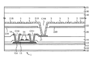
本発明の第1の実施の形態について図面を参照しながら説明する。図1は液晶表示装置の表示領域の一部の平面図であり、図2は図1のX1−X1線に沿った断面図である。実際の液晶表示装置の表示領域70においては、多数の画素がマトリクスに配置されているが、これらの図では3画素のみを示している。
First Embodiment A first embodiment of the present invention will be described with reference to the drawings. FIG. 1 is a plan view of a part of the display area of the liquid crystal display device, and FIG. 2 is a cross-sectional view taken along line X1-X1 in FIG. In the
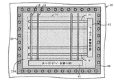
画素電極21は第1層透明電極で形成され、絶縁膜22を間に挟んでその上層に、第2層透明電極からなる共通電極23Aが形成される。そして、上層の共通電極23Aに複数のスリットSが設けられる。以上の点は従来例(図20を参照)と同じであるが、本実施の形態においては、共通電極23Aは表示領域70の全ての画素に跨っている。共通電極23Aの端部は、表示領域70の外周に配置され、共通電位Vcomを供給する外周共通電位ライン50に接続されている。
The
その接続断面構造は、図2に示すように、外周共通電位ライン50は表示信号ライン18等と同じ層で形成されており、アルミニウムもしくはアルミニウム合金を含む金属等からなる。外周共通電位ライン50は層間絶縁膜16上に形成され、その上層の平坦化膜20及び絶縁膜22に形成されたコンタクトホールCH7を通して、上層の共通電極23Aが外周共通電位ライン50に接続されている。外周共通電位ライン50は、TFT基板10上の不図示の端子に接続され、その端子を介して、TFT基板10の外部のIC等から共通電位Vcomが供給される。
As shown in FIG. 2, the outer peripheral common
また、本実施の形態の液晶表示装置によれば、従来例のような共通電極補助ライン15、パッド電極19は設けられていない。そのため、画素の開口率が向上する。また、共通電極23Aは表示領域70の全ての画素に跨るように一体化されており、その端部を外周共通電位ライン50に接続したので、共通電極23Aに共通電位Vcomを低抵抗で十分に供給することができる。
Further, according to the liquid crystal display device of the present embodiment, the common electrode
外周共通電位ライン50は、図3のレイアウト例では矩形の表示領域70の1辺に沿って、表示領域70の外周に配置されている。共通電極23Aにさらに低抵抗で共通電位Vcomを供給するためには、図4のレイアウト例のように、外周共通電位ライン50を対向する2辺に沿って配置し、それぞれの辺の外周共通電位ライン50と共通電極23Aの端部とを接続することが好ましい。この場合、図5のレイアウト例のように、外周共通電位ライン50を隣接する2辺に沿って配置してもよい。
The outer periphery common
共通電極23Aにさらに低抵抗で共通電位Vcomを供給するためには、図6のレイアウト例のように、3辺に沿って配置し、あるいは、図7のように4辺に沿って配置し、それぞれの辺の外周共通電位ライン50と共通電極23Aの端部とを接続することが好ましい。
In order to supply the common potential Vcom to the
しかしながら、図7のように表示領域70を外周共通電位ライン50で取り囲むレイアウトでは、ゲートライン14と表示信号ライン18を外周共通電位ライン50の外に取り出す必要がある。これは、ゲートライン14と表示信号ライン18をそれぞれ信号源に接続するためである。
However, in the layout in which the
すると、外周共通電位ライン50と表示信号ライン18とが同じ層である場合には、図中の破線で囲んだ部分のように、外周共通電位ライン50と表示信号ライン18の交差部において短絡を防止するために、どちらかのラインの層を部分的に変更してブリッジを形成する必要がある。例えば、交差部では表示信号ライン18をゲートライン14と同じ層に変更することになる。ゲートライン14については、外周共通電位ライン50と異なる層であるから、外周共通電位ライン50と交差させている。
Then, when the outer periphery common
そのようなブリッジや交差を避けるためには、図8のように、信号源となる回路を外周共通電位ライン50で囲まれたスペースに配置すればよい。すなわち、表示信号ライン18に表示信号を供給する表示信号ライン制御回路61、ゲートライン14にゲート信号を供給するゲートライン制御回路62を表示領域70と外周共通電位ライン50との間のスペースに配置する。
In order to avoid such a bridge or intersection, a circuit serving as a signal source may be disposed in a space surrounded by the outer peripheral common
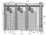
第2の実施の形態
本発明の第2の実施の形態について図面を参照しながら説明する。図9は液晶表示装置の表示領域の一部の平面図であり、図10は図9のX2−X2線に沿った断面図である。また、図11は図9のY1―Y1線に沿った断面図である。実際の液晶表示装置の表示領域においては、多数の画素がマトリクスに配置されているが、これらの図では3画素のみを示している。
Second Embodiment A second embodiment of the present invention will be described with reference to the drawings. FIG. 9 is a plan view of a part of the display area of the liquid crystal display device, and FIG. 10 is a cross-sectional view taken along line X2-X2 of FIG. FIG. 11 is a sectional view taken along line Y1-Y1 of FIG. In a display area of an actual liquid crystal display device, a large number of pixels are arranged in a matrix, but only three pixels are shown in these drawings.
本実施の形態は、第1の実施の形態の画素電極21と共通電極23Aの上下の配置関係を逆転させたものであり、共通電極23Bが第1層透明電極で形成され、絶縁膜22を間に挟んでその上層に、画素電極21Bが第2層透明電極で形成される。そして、上層の画素電極21Bに複数のスリットSが設けられる。
In this embodiment, the upper and lower arrangement relationship of the
このような画素の構成においても、画素電極21Bと共通電極23Bの間に横方向電界を生じさせて液晶分子の配向方向を制御することで広視野角の液晶表示を得ることができる。
Even in such a pixel configuration, a wide viewing angle liquid crystal display can be obtained by controlling the alignment direction of liquid crystal molecules by generating a horizontal electric field between the
画素電極21Bは画素毎に分断され、各画素のTFT1のソース電極17に接続されている。共通電極23Bは第1の実施の形態と同様に、表示領域70の全ての画素に跨っている。共通電極23Bの端部は、表示領域70の外周に配置され、共通電位Vcomを供給する外周共通電位ライン50に接続されている。
The
その接続断面構造は、図10に示すように、外周共通電位ライン50は表示信号ライン18等と同じ層で形成されており、アルミニウムもしくはアルミニウム合金を含む金属等からなる。外周共通電位ライン50は層間絶縁膜16上に形成され、その上層の平坦化膜20に形成されたコンタクトホールCH8を通して、共通電極23Bが外周共通電位ライン50に接続されている。外周共通電位ライン50は、TFT基板10上の不図示の端子に接続され、その端子を介して、TFT基板10の外部のIC等から共通電位Vcomが供給される。
As shown in FIG. 10, the outer peripheral common
その他の構成については、第1の実施の形態と全く同じである。すなわち、外周共通電位ライン50、共通電極23Bのレイアウトは図3〜図8のレイアウトを適用することができ、同様の効果を得ることができる。
Other configurations are the same as those in the first embodiment. That is, the layout of FIGS. 3 to 8 can be applied to the layout of the outer periphery common
第3の実施の形態
本発明の第3の実施の形態について図面を参照しながら説明する。第1、第2の実施の形態においては、画素内のTFT1は能動層がポリシリコンで形成されたポリシリコンTFTであるが、本実施の形態ではその代わりに、能動層がアモルファスシリコンで形成されたアモルファスシリコンTFT1a(以下、aSi−TFT1aという)が用いられている。
Third embodiment
A third embodiment of the present invention will be described with reference to the drawings. In the first and second embodiments, the TFT 1 in the pixel is a polysilicon TFT whose active layer is formed of polysilicon, but in this embodiment, the active layer is formed of amorphous silicon instead. An amorphous silicon TFT 1a (hereinafter referred to as aSi-TFT 1a ) is used.
図12はこの液晶表示装置の表示領域の一部の平面図であり、図13は図12のX3−X3線に沿った断面図である。また、図14は図12のY2―Y2線に沿った断面図である。実際の液晶表示装置の表示領域においては、多数の画素がマトリクスに配置されているが、これらの図では3画素のみを示している。 FIG. 12 is a plan view of a part of the display area of the liquid crystal display device, and FIG. 13 is a cross-sectional view taken along line X3-X3 in FIG. FIG. 14 is a sectional view taken along line Y2-Y2 of FIG. In a display area of an actual liquid crystal display device, a large number of pixels are arranged in a matrix, but only three pixels are shown in these drawings.
TFT基板100上にaSi−TFT1aのゲートライン114が形成される。ゲートライン114はクロム、モリブデン等で形成される。ゲートライン114を除く領域にストライプ状に複数の画素に跨って延びた共通電極123Bが形成される。共通電極123BはITO等の第1層透明電極で形成される。そして、ゲートライン114、共通電極123Bを覆って、ゲート絶縁膜101が形成される。ゲート絶縁膜101上に、ゲートライン114を覆ってアモルファスシリコン層102が形成される。そして、アモルファスシリコン層102に接触して表示信号ライン118(ドレイン電極)とソース電極103が形成される。
On the
全面に層間絶縁膜104が形成され、ソース電極103上の層間絶縁膜104が部分的にエッチングされ、コンタクトホールCH12が形成される。このコンタクトホールCH12を通してソース電極103に接続された画素電極121Bが形成される。画素電極121Bは、ITO等の第2層透明電極からなり、複数のスリットSを有している。そして、画素電極121Bはゲート絶縁膜101及び層間絶縁膜104を間に挟んで共通電極123B上に形成される。
An interlayer insulating
このようなaSi−TFT1aを用いた画素の構成においても、画素電極121Bと共通電極123Bの間に横方向電界を生じさせて液晶分子の配向方向を制御することで広視野角の液晶表示を得ることができる。
Even in the configuration of a pixel using such an aSi-TFT 1a, a liquid crystal display with a wide viewing angle is obtained by controlling the alignment direction of liquid crystal molecules by generating a horizontal electric field between the
また、共通電極123Bの端部は表示領域70の外周に配置され、共通電位Vcomを供給する外周共通電位ライン150に接続されている。その接続断面構造は、図13に示すように、外周共通電位ライン150は表示信号ライン118等と同じ層で形成されており、アルミニウムもしくはアルミニウム合金を含む金属等からなる。外周共通電位ライン150はゲート絶縁膜101上に形成されている。そして、共通電極123B上のゲート絶縁膜101及び層間絶縁膜104に形成されたコンタクトホールCH13、外周共通電位ライン150上の層間絶縁膜104に形成されたコンタクトホールCH14を介して、第2層透明電極からなる接続用配線119によって、共通電極123Bと外周共通電位ライン150が接続されている。
Further, the end portion of the
外周共通電位ライン150は、TFT基板100上の不図示の端子に接続され、その端子を介して、TFT基板100の外部のIC等から共通電位Vcomが供給される。
The outer peripheral common
なお、TFT基板100と対向して対向基板が設けられ、TFT基板100と対向基板との間に液晶が封入されるなどの点については、第1、2の実施の形態と同様であるので詳細な説明は省略する。
Since the counter substrate is provided opposite to the
本実施の形態の液晶表示装置によれば、第1、第2の実施の形態と同様に、共通電極補助ライン15、パッド電極19は設けられていない。そのため、画素の開口率が向上する。また、共通電極123Bは表示領域70の全ての画素に跨るように一体化されており、その端部を外周共通電位ライン150に接続したので、共通電極123Bに共通電位Vcomを低抵抗で十分に供給することができる。また、外周共通電位ライン150、共通電極123Bのレイアウトについても同様に図3〜図8のレイアウトを適用することができ、同様の効果を得ることができる。
According to the liquid crystal display device of the present embodiment, the common electrode
第4の実施の形態
本発明の第4の実施の形態について図面を参照しながら説明する。図15はこの液晶表示装置の表示領域の一部の平面図であり、図16は図15のX4−X4線に沿った断面図である。また、図16は図15のY3―Y3線に沿った断面図である。実際の液晶表示装置の表示領域においては、多数の画素がマトリクスに配置されているが、これらの図では3画素のみを示している。
Fourth embodiment
A fourth embodiment of the present invention will be described with reference to the drawings. FIG. 15 is a plan view of a part of the display area of the liquid crystal display device, and FIG. 16 is a cross-sectional view taken along line X4-X4 of FIG. Further, FIG. 16 is a sectional view taken along line Y3-Y3 of FIG. In a display area of an actual liquid crystal display device, a large number of pixels are arranged in a matrix, but only three pixels are shown in these drawings.
本実施の形態は、第3の実施の形態の画素電極121Bと共通電極123Bの上下の配置関係を逆転させたものであり、画素電極121Aが第1層透明電極で形成され、ゲート絶縁膜101、層間絶縁膜104を間に挟んでその上層に、共通電極123Aが第2層透明電極で形成される。そして、上層の共通電極123Aに複数のスリットSが設けられる。
In the present embodiment, the
共通電極123Aの端部は表示領域70の外周に配置され、共通電位Vcomを供給する外周共通電位ライン150に接続されている。その接続断面構造は、図16に示すように、外周共通電位ライン150は表示信号ライン118等と同じ層で形成されており、アルミニウムもしくはアルミニウム合金を含む金属等からなる。外周共通電位ライン150はゲート絶縁膜101上に形成されている。そして、外周共通電位ライン150上の層間絶縁膜104に形成されたコンタクトホールCH15を介して、共通電極123Aと外周共通電位ライン150が接続されている。その他の点については、第3の実施の形態と同様である。
An end portion of the
なお、第1乃至第4の実施の形態において、共通電極23A、123AのスリットSは1つの画素内に形成されているが、スリットSは複数の画素に跨って、繋がっていてもよい。また画素電極21B、121Bは、スリットSの一方の端部が開口された櫛歯形状であってもよい。
In the first to fourth embodiments, the slits S of the
1 TFT 1a aSi−TFT
10,100 TFT基板 11 バッファ層
12 能動層 12d ドレイン領域
12s ソース領域 13,101 ゲート絶縁膜
14,114 ゲートライン 15 共通電極補助ライン
16,104 層間絶縁膜 17,103 ソース電極
18,118 表示信号ライン 19 パッド電極
20 平坦化膜 21,21B,121A,121B 画素電極
22 絶縁膜 23,23A,23B,123A,123B 共通電極
30 対向基板 31,32 偏光板
40 液晶 50 外周共通電位ライン
61 表示信号ライン制御回路 62 ゲートライン制御回路
70 表示領域 102 アモルファスシリコン層
119 接続用配線 150 外周共通電位ライン
CH1〜CH15 コンタクトホール S スリット
1 TFT 1a aSi-TFT
DESCRIPTION OF SYMBOLS 10,100
Claims (5)
前記基板上の表示領域に配置された複数の画素と、
前記表示領域の四辺に沿って前記表示領域の外周に配置され、透明電極からなる共通電極に共通電位を供給する外周共通電位ラインと、を備え、
各画素は、画素電極と、この画素電極上に絶縁膜を介して配置され、複数のスリットを有し、複数の画素に跨って配置された前記共通電極とを備え、
前記外周共通電位ラインは、前記表示領域の四辺に沿った外周において、前記共通電極の端部と複数のコンタクトホールを介して接続され、前記外周共通電位ラインの全体は、前記画素に表示信号を供給する表示信号ラインと同じ層であることを特徴とする液晶表示装置。 A substrate,
A plurality of pixels arranged in a display area on the substrate;
An outer periphery common potential line arranged on the outer periphery of the display region along the four sides of the display region and supplying a common potential to a common electrode made of a transparent electrode,
Each pixel includes a pixel electrode and the common electrode that is disposed on the pixel electrode via an insulating film, has a plurality of slits, and is disposed across the plurality of pixels.
The outer periphery common potential line is connected to the end of the common electrode through a plurality of contact holes on the outer periphery along the four sides of the display region, and the entire outer periphery common potential line transmits a display signal to the pixel. A liquid crystal display device having the same layer as a display signal line to be supplied.
前記基板上の表示領域に配置された複数の画素と、
前記表示領域の四辺に沿って前記表示領域の外周に配置され、透明電極からなる共通電極に共通電位を供給する外周共通電位ラインと、を備え、
各画素は、複数の画素に跨って配置された前記共通電極と、この共通電極上に絶縁膜を介して配置され、複数のスリットを有する画素電極とを備え、
前記外周共通電位ラインは、前記表示領域の四辺に沿った外周において、前記共通電極の端部と複数のコンタクトホールを介して接続され、前記外周共通電位ラインの全体は、前記画素に表示信号を供給する表示信号ラインと同じ層であることを特徴とする液晶表示装置。 A substrate,
A plurality of pixels arranged in a display area on the substrate;
An outer periphery common potential line arranged on the outer periphery of the display region along the four sides of the display region and supplying a common potential to a common electrode made of a transparent electrode,
Each pixel includes the common electrode disposed across a plurality of pixels, and a pixel electrode disposed on the common electrode via an insulating film and having a plurality of slits,
The outer periphery common potential line is connected to the end of the common electrode through a plurality of contact holes on the outer periphery along the four sides of the display region, and the entire outer periphery common potential line transmits a display signal to the pixel. A liquid crystal display device having the same layer as a display signal line to be supplied.
Priority Applications (15)
| Application Number | Priority Date | Filing Date | Title |
|---|---|---|---|
| JP2006204624A JP4449953B2 (en) | 2006-07-27 | 2006-07-27 | Liquid crystal display |
| TW096124419A TWI369558B (en) | 2006-07-27 | 2007-07-05 | Liquid crystal display device |
| US11/878,579 US20080024416A1 (en) | 2006-07-27 | 2007-07-25 | Liquid crystal display device |
| KR1020070075037A KR100884126B1 (en) | 2006-07-27 | 2007-07-26 | Liquid crystal display device |
| CNB2007101392005A CN100510913C (en) | 2006-07-27 | 2007-07-27 | Liquid crystal display device |
| US13/493,618 US9291863B2 (en) | 2006-07-27 | 2012-06-11 | Liquid crystal display device |
| US15/134,677 US10126608B2 (en) | 2006-07-27 | 2016-04-21 | Liquid crystal display device |
| US15/162,110 US9946125B2 (en) | 2006-07-27 | 2016-05-23 | Liquid crystal display device |
| US15/423,209 US10126609B2 (en) | 2006-07-27 | 2017-02-02 | Liquid crystal display device |
| US16/163,794 US10802353B2 (en) | 2006-07-27 | 2018-10-18 | Liquid crystal display device |
| US16/521,247 US10606133B2 (en) | 2006-07-27 | 2019-07-24 | Liquid crystal display device |
| US16/521,228 US11543708B2 (en) | 2006-07-27 | 2019-07-24 | Display device including common line display device including common line |
| US16/995,368 US11143923B2 (en) | 2006-07-27 | 2020-08-17 | Display device |
| US17/068,039 US11698555B2 (en) | 2006-07-27 | 2020-10-12 | Display device |
| US18/196,725 US20230280619A1 (en) | 2006-07-27 | 2023-05-12 | Display device |
Applications Claiming Priority (1)
| Application Number | Priority Date | Filing Date | Title |
|---|---|---|---|
| JP2006204624A JP4449953B2 (en) | 2006-07-27 | 2006-07-27 | Liquid crystal display |
Publications (3)
| Publication Number | Publication Date |
|---|---|
| JP2008032899A JP2008032899A (en) | 2008-02-14 |
| JP2008032899A5 JP2008032899A5 (en) | 2008-04-10 |
| JP4449953B2 true JP4449953B2 (en) | 2010-04-14 |
Family
ID=38985665
Family Applications (1)
| Application Number | Title | Priority Date | Filing Date |
|---|---|---|---|
| JP2006204624A Active JP4449953B2 (en) | 2006-07-27 | 2006-07-27 | Liquid crystal display |
Country Status (5)
| Country | Link |
|---|---|
| US (11) | US20080024416A1 (en) |
| JP (1) | JP4449953B2 (en) |
| KR (1) | KR100884126B1 (en) |
| CN (1) | CN100510913C (en) |
| TW (1) | TWI369558B (en) |
Families Citing this family (81)
| Publication number | Priority date | Publication date | Assignee | Title |
|---|---|---|---|---|
| JP4449953B2 (en) | 2006-07-27 | 2010-04-14 | エプソンイメージングデバイス株式会社 | Liquid crystal display |
| JP5216204B2 (en) | 2006-10-31 | 2013-06-19 | 株式会社半導体エネルギー研究所 | Liquid crystal display device and manufacturing method thereof |
| JP5275650B2 (en) * | 2008-03-12 | 2013-08-28 | 株式会社ジャパンディスプレイウェスト | Liquid crystal display |
| JP2009223245A (en) * | 2008-03-19 | 2009-10-01 | Hitachi Displays Ltd | Liquid crystal display device |
| JP5348521B2 (en) | 2008-06-27 | 2013-11-20 | 株式会社ジャパンディスプレイ | LCD panel |
| JP5348384B2 (en) * | 2008-10-01 | 2013-11-20 | 株式会社ジャパンディスプレイ | Liquid crystal display |
| TWI613489B (en) | 2008-12-03 | 2018-02-01 | 半導體能源研究所股份有限公司 | Liquid crystal display device |
| WO2010131552A1 (en) * | 2009-05-13 | 2010-11-18 | シャープ株式会社 | Liquid crystal display device |
| JP5389529B2 (en) * | 2009-05-20 | 2014-01-15 | 株式会社ジャパンディスプレイ | Liquid crystal display device and manufacturing method thereof |
| KR101857405B1 (en) * | 2009-07-10 | 2018-05-11 | 가부시키가이샤 한도오따이 에네루기 켄큐쇼 | Semiconductor device and method for manufacturing the same |
| US20110085121A1 (en) * | 2009-10-08 | 2011-04-14 | Hydis Technologies Co., Ltd. | Fringe Field Switching Mode Liquid Crystal Display Device and Method of Fabricating the Same |
| KR101790977B1 (en) * | 2010-10-08 | 2017-10-26 | 엘지디스플레이 주식회사 | Liquid crystal display device |
| KR101891985B1 (en) * | 2010-10-08 | 2018-08-27 | 엘지디스플레이 주식회사 | Liquid crystal display device |
| CN102129143A (en) * | 2010-12-15 | 2011-07-20 | 华映视讯(吴江)有限公司 | Pixel array substrate and manufacturing method thereof |
| KR101924473B1 (en) * | 2010-12-28 | 2018-12-03 | 엘지디스플레이 주식회사 | Thin film transistor array substrate and method thereof |
| KR101870986B1 (en) * | 2011-09-19 | 2018-06-26 | 엘지디스플레이 주식회사 | Method for fabricating thin film transistor array substrate |
| WO2013073619A1 (en) | 2011-11-18 | 2013-05-23 | シャープ株式会社 | Semiconductor device, display device, and method for producing semiconductor device |
| WO2013077262A1 (en) * | 2011-11-25 | 2013-05-30 | シャープ株式会社 | Liquid crystal display device |
| US9343580B2 (en) | 2011-12-05 | 2016-05-17 | Sharp Kabushiki Kaisha | Semiconductor device |
| US10048551B2 (en) | 2012-01-11 | 2018-08-14 | Sharp Kabushiki Kaisha | Semiconductor device, display device, and semiconductor device manufacturing method |
| SG11201404927YA (en) | 2012-02-15 | 2014-10-30 | Sharp Kk | Liquid crystal display |
| JP5912668B2 (en) * | 2012-03-01 | 2016-04-27 | シャープ株式会社 | Liquid crystal display |
| CN102651342B (en) | 2012-03-13 | 2014-12-17 | 京东方科技集团股份有限公司 | Array substrate and manufacturing method thereof |
| CN102790051B (en) * | 2012-07-27 | 2014-12-10 | 北京京东方光电科技有限公司 | Array substrate and preparation method and display device thereof |
| CN102944959B (en) * | 2012-11-20 | 2014-12-24 | 京东方科技集团股份有限公司 | Array substrate, producing method and testing method thereof and display device |
| US9368521B2 (en) | 2012-11-30 | 2016-06-14 | Sharp Kabushiki Kaisha | TFT substrate |
| TWI636309B (en) * | 2013-07-25 | 2018-09-21 | 日商半導體能源研究所股份有限公司 | Liquid crystal display device and electronic device |
| TWI506501B (en) * | 2013-08-30 | 2015-11-01 | Ye Xin Technology Consulting Co Ltd | Electronic device |
| JP5714679B2 (en) * | 2013-10-17 | 2015-05-07 | 株式会社ジャパンディスプレイ | Liquid crystal display |
| CN103529605A (en) * | 2013-10-29 | 2014-01-22 | 京东方科技集团股份有限公司 | Array substrate, manufacturing method thereof, display panel and display device |
| WO2015092944A1 (en) * | 2013-12-19 | 2015-06-25 | パナソニック液晶ディスプレイ株式会社 | Display device and method for manufacturing display device |
| WO2015125685A1 (en) | 2014-02-21 | 2015-08-27 | シャープ株式会社 | Active matrix substrate and method for producing same |
| JP6400935B2 (en) * | 2014-04-17 | 2018-10-03 | 株式会社ジャパンディスプレイ | Display device |
| US9958720B2 (en) | 2014-04-17 | 2018-05-01 | Japan Display Inc. | Display device |
| CN104201178B (en) * | 2014-08-08 | 2017-04-05 | 京东方科技集团股份有限公司 | Array base palte and preparation method thereof, display device |
| CN104216183B (en) * | 2014-08-28 | 2017-08-29 | 合肥鑫晟光电科技有限公司 | A kind of array base palte and preparation method thereof, display device |
| CN104280951A (en) * | 2014-09-23 | 2015-01-14 | 京东方科技集团股份有限公司 | Array substrate, manufacturing method thereof, and display device |
| TWI567950B (en) * | 2015-01-08 | 2017-01-21 | 群創光電股份有限公司 | Display panels |
| CN105824160B (en) * | 2015-01-08 | 2020-06-16 | 群创光电股份有限公司 | Display panel |
| TWI577000B (en) | 2015-01-21 | 2017-04-01 | 群創光電股份有限公司 | Display device |
| KR102381082B1 (en) * | 2015-07-31 | 2022-03-30 | 엘지디스플레이 주식회사 | Liquid crystal display apparatus |
| WO2017026372A1 (en) | 2015-08-10 | 2017-02-16 | シャープ株式会社 | Active matrix substrate and method for producing same, and in-cell touch panel-type display device |
| TWI564644B (en) * | 2015-08-28 | 2017-01-01 | 群創光電股份有限公司 | Display device |
| CN105261621B (en) * | 2015-09-06 | 2018-01-30 | 京东方科技集团股份有限公司 | Array base palte and preparation method thereof, display device |
| CN105204252A (en) * | 2015-09-23 | 2015-12-30 | 深超光电(深圳)有限公司 | Thin film transistor array substrate and liquid crystal display panel |
| CN108352358B (en) | 2015-10-13 | 2022-07-26 | 非结晶公司 | Non-linear resistor of amorphous metal film |
| KR102473647B1 (en) * | 2015-12-29 | 2022-12-01 | 엘지디스플레이 주식회사 | Liquid crystal display device |
| TWI561891B (en) | 2016-01-04 | 2016-12-11 | Au Optronics Corp | Pixel array substrate |
| WO2017150443A1 (en) | 2016-03-02 | 2017-09-08 | シャープ株式会社 | Active matrix substrate, and liquid crystal display device provided with active matrix substrate |
| WO2017159625A1 (en) | 2016-03-15 | 2017-09-21 | シャープ株式会社 | Active matrix substrate |
| US10725336B2 (en) * | 2016-05-20 | 2020-07-28 | Sharp Kabushiki Kaisha | Liquid crystal display panel and liquid crystal display device |
| CN105807523B (en) | 2016-05-27 | 2020-03-20 | 厦门天马微电子有限公司 | Array substrate, display panel comprising same and display device |
| TW201743118A (en) | 2016-06-08 | 2017-12-16 | 群創光電股份有限公司 | Display panel |
| WO2018030298A1 (en) | 2016-08-12 | 2018-02-15 | シャープ株式会社 | Active-matrix substrate and display device |
| CN109661701A (en) | 2016-09-01 | 2019-04-19 | 夏普株式会社 | Active-matrix substrate and display device |
| CN109690661B (en) | 2016-09-02 | 2021-01-01 | 夏普株式会社 | Active matrix substrate and display device provided with active matrix substrate |
| US10714552B2 (en) | 2016-09-05 | 2020-07-14 | Sharp Kabushiki Kaisha | Active matrix substrate having plurality of circuit thin film transistors and pixel thin film transistors |
| CN106502012A (en) * | 2017-01-03 | 2017-03-15 | 深圳市华星光电技术有限公司 | Array base palte of FFS mode and preparation method thereof |
| WO2018139450A1 (en) | 2017-01-27 | 2018-08-02 | シャープ株式会社 | Active matrix substrate and display device using same |
| CN110291644B (en) | 2017-02-15 | 2022-11-01 | 夏普株式会社 | Active matrix substrate |
| WO2018163997A1 (en) | 2017-03-09 | 2018-09-13 | シャープ株式会社 | Active matrix substrate and method for producing same |
| WO2018212100A1 (en) | 2017-05-18 | 2018-11-22 | シャープ株式会社 | Active matrix substrate and production method therefor |
| CN107422552B (en) * | 2017-08-16 | 2020-03-27 | 京东方科技集团股份有限公司 | Display substrate and display device |
| CN107302665B (en) * | 2017-08-18 | 2020-07-24 | 联想(北京)有限公司 | Camera device, aperture adjusting method and electronic equipment |
| JP2019049590A (en) | 2017-09-08 | 2019-03-28 | シャープ株式会社 | Active matrix substrate and de-multiplexer circuit |
| JP2019050323A (en) | 2017-09-12 | 2019-03-28 | シャープ株式会社 | Active matrix substrate and demultiplexer circuit |
| JP7066445B2 (en) * | 2018-02-20 | 2022-05-13 | 株式会社ジャパンディスプレイ | Display device |
| JP6496433B2 (en) * | 2018-02-27 | 2019-04-03 | 株式会社半導体エネルギー研究所 | Liquid crystal display |
| JP6706638B2 (en) | 2018-03-07 | 2020-06-10 | シャープ株式会社 | Semiconductor device and manufacturing method thereof |
| TWI809075B (en) * | 2018-03-30 | 2023-07-21 | 美商非結晶公司 | Electronic device and a display with the same |
| CN108983484A (en) * | 2018-08-06 | 2018-12-11 | 深圳市华星光电技术有限公司 | A kind of colored filter and preparation method, display device |
| JP6799123B2 (en) | 2018-09-19 | 2020-12-09 | シャープ株式会社 | Active matrix substrate and its manufacturing method |
| WO2020065866A1 (en) * | 2018-09-27 | 2020-04-02 | シャープ株式会社 | Display device |
| CN109521613A (en) * | 2018-12-24 | 2019-03-26 | 上海天马微电子有限公司 | A kind of array substrate, its production method, display panel and display device |
| CN109742088B (en) * | 2018-12-29 | 2021-03-16 | 武汉华星光电技术有限公司 | TFT array substrate |
| US10928691B2 (en) * | 2019-02-15 | 2021-02-23 | Sharp Kabushiki Kaisha | Active matrix substrate comprising a first contact hole that overlaps with a counter electrode control line and passes through a flattening film and liquid crystal display with the same |
| JP7471075B2 (en) | 2019-12-17 | 2024-04-19 | シャープ株式会社 | Active matrix substrate and its manufacturing method |
| US11557679B2 (en) | 2020-03-02 | 2023-01-17 | Sharp Kabushiki Kaisha | Active matrix substrate and display device |
| CN111983862B (en) * | 2020-08-19 | 2022-07-12 | 武汉华星光电技术有限公司 | Array substrate, array substrate manufacturing method and liquid crystal display panel |
| JP2023036194A (en) * | 2021-09-02 | 2023-03-14 | 株式会社ジャパンディスプレイ | Display device |
| CN115437187B (en) | 2022-11-09 | 2023-03-24 | 惠科股份有限公司 | Array substrate and display panel |
Family Cites Families (86)
| Publication number | Priority date | Publication date | Assignee | Title |
|---|---|---|---|---|
| TW354380B (en) * | 1995-03-17 | 1999-03-11 | Hitachi Ltd | A liquid crystal device with a wide visual angle |
| US6078318A (en) * | 1995-04-27 | 2000-06-20 | Canon Kabushiki Kaisha | Data transfer method, display driving circuit using the method, and image display apparatus |
| JP3582193B2 (en) | 1995-12-08 | 2004-10-27 | カシオ計算機株式会社 | Liquid crystal display device |
| JP3170446B2 (en) | 1996-02-27 | 2001-05-28 | シャープ株式会社 | Active matrix substrate and liquid crystal display |
| US5852485A (en) * | 1996-02-27 | 1998-12-22 | Sharp Kabushiki Kaisha | Liquid crystal display device and method for producing the same |
| JPH10133234A (en) | 1996-09-04 | 1998-05-22 | Toshiba Corp | Liquid crystal display device |
| US20020075422A1 (en) * | 1996-09-19 | 2002-06-20 | Seiko Epson Corporation | Matrix type display device and manufacturing method thereof |
| US6532053B2 (en) | 1996-12-18 | 2003-03-11 | Hitachi, Ltd. | Transverse electric field system liquid crystal display device suitable for improving aperture ratio |
| JPH10186351A (en) | 1996-12-24 | 1998-07-14 | Hitachi Ltd | Liquid crystal display device |
| JP4024901B2 (en) * | 1997-05-22 | 2007-12-19 | エルジー フィリップス エルシーディー カンパニー リミテッド | Active matrix type liquid crystal display device |
| KR100251512B1 (en) * | 1997-07-12 | 2000-04-15 | 구본준 | In-plane switching mode lcd |
| KR100280874B1 (en) | 1997-09-12 | 2001-02-01 | 구본준 | LCD panel |
| JP3831863B2 (en) * | 1997-10-21 | 2006-10-11 | 大林精工株式会社 | Liquid crystal display |
| WO1999023530A1 (en) * | 1997-10-31 | 1999-05-14 | Seiko Epson Corporation | Electro-optical device and electronic apparatus |
| CN100409088C (en) * | 1997-11-03 | 2008-08-06 | 三星电子株式会社 | Liquid crystal display with changed electrode arrange |
| JPH11326928A (en) * | 1998-05-08 | 1999-11-26 | Hitachi Ltd | Liquid crystal display device |
| JP3766563B2 (en) | 1999-05-17 | 2006-04-12 | 株式会社日立製作所 | Liquid crystal display |
| JP3481509B2 (en) | 1999-06-16 | 2003-12-22 | Nec液晶テクノロジー株式会社 | Liquid crystal display |
| JP2001083546A (en) * | 1999-07-12 | 2001-03-30 | Hitachi Ltd | Liquid crystal display device |
| TW457384B (en) * | 1999-09-13 | 2001-10-01 | Ind Tech Res Inst | Electrode structure for a wide viewing angle liquid crystal display |
| TWI288284B (en) * | 1999-09-16 | 2007-10-11 | Sharp Kk | Liquid crystal display device and thin film transistor substrate |
| CN1195243C (en) * | 1999-09-30 | 2005-03-30 | 三星电子株式会社 | Film transistor array panel for liquid crystal display and its producing method |
| JP2001102169A (en) * | 1999-10-01 | 2001-04-13 | Sanyo Electric Co Ltd | El display |
| JP3379491B2 (en) * | 1999-10-22 | 2003-02-24 | 日本電気株式会社 | Liquid crystal display |
| JP3687452B2 (en) | 1999-12-27 | 2005-08-24 | 株式会社日立製作所 | Liquid crystal display device |
| JP3832261B2 (en) | 2000-03-16 | 2006-10-11 | セイコーエプソン株式会社 | Liquid crystal device, projection display device, and electronic apparatus |
| JP2001272697A (en) | 2000-03-23 | 2001-10-05 | Hitachi Ltd | Liquid crystal display device |
| US6500701B2 (en) * | 2000-04-28 | 2002-12-31 | Casio Computer Co., Ltd. | Method of manufacturing thin film transistor panel having protective film of channel region |
| KR100633315B1 (en) * | 2000-06-01 | 2006-10-11 | 엘지.필립스 엘시디 주식회사 | Structure of common line for LCD and Storage line for in plain switching mode LCD |
| JP2001354968A (en) | 2000-06-09 | 2001-12-25 | Hitachi Ltd | Active matrix liquid crystal display device and its liquid crystal composition substance |
| JP4446577B2 (en) * | 2000-09-06 | 2010-04-07 | エーユー オプトロニクス コーポレイション | Display panel, display device |
| KR100601454B1 (en) | 2000-10-04 | 2006-07-14 | 엘지.필립스 엘시디 주식회사 | Multi-domain liquid crystal display and method for manufacturing thereof |
| US6784966B2 (en) * | 2001-03-06 | 2004-08-31 | Seiko Epson Corp. | Liquid crystal device, projection type display and electronic equipment |
| JP4556341B2 (en) | 2001-03-30 | 2010-10-06 | セイコーエプソン株式会社 | Liquid crystal display device and electronic device |
| JP3618302B2 (en) | 2001-04-10 | 2005-02-09 | 松下電器産業株式会社 | Inspection method and inspection device for liquid crystal panel |
| JP4041336B2 (en) * | 2001-06-29 | 2008-01-30 | シャープ株式会社 | Substrate for liquid crystal display device, liquid crystal display device including the same, and manufacturing method thereof |
| JP4353660B2 (en) | 2001-07-27 | 2009-10-28 | 三洋電機株式会社 | Active matrix display device |
| JP2003090994A (en) | 2001-09-19 | 2003-03-28 | Hitachi Ltd | Liquid crystal display device |
| JP3909572B2 (en) * | 2001-09-28 | 2007-04-25 | 株式会社日立製作所 | Display device |
| US6778229B2 (en) * | 2001-10-02 | 2004-08-17 | Fujitsu Display Technologies Corporation | Liquid crystal display device and method of fabricating the same |
| JP4305811B2 (en) * | 2001-10-15 | 2009-07-29 | 株式会社日立製作所 | Liquid crystal display device, image display device and manufacturing method thereof |
| JP2003131248A (en) | 2001-10-25 | 2003-05-08 | Seiko Epson Corp | Liquid crystal display device and manufacturing method therefor, and substrate therefor, and electronic equipment |
| KR100652046B1 (en) * | 2001-12-22 | 2006-11-30 | 엘지.필립스 엘시디 주식회사 | A Liquid Crystal Display Device And The Method For Manufacturing The Same |
| KR100450701B1 (en) * | 2001-12-28 | 2004-10-01 | 엘지.필립스 엘시디 주식회사 | The substrate for LCD and method for fabricating the same |
| JP3920649B2 (en) | 2002-01-31 | 2007-05-30 | 株式会社日立製作所 | Image display device and liquid crystal display device |
| US7102726B2 (en) * | 2002-03-15 | 2006-09-05 | Lg. Philips Lcd Co., Ltd. | System for fabricating liquid crystal display and method of fabricating liquid crystal display using the same |
| JP2003295207A (en) | 2002-03-29 | 2003-10-15 | Nec Lcd Technologies Ltd | Active matrix type liquid crystal display device of transverse electric field system |
| JP4005410B2 (en) | 2002-05-15 | 2007-11-07 | 株式会社 日立ディスプレイズ | Image display device |
| JP3778176B2 (en) * | 2002-05-28 | 2006-05-24 | セイコーエプソン株式会社 | LIGHT EMITTING DEVICE AND ELECTRONIC DEVICE |
| JP4085170B2 (en) * | 2002-06-06 | 2008-05-14 | 株式会社 日立ディスプレイズ | Liquid crystal display |
| JP3700714B2 (en) * | 2002-06-21 | 2005-09-28 | セイコーエプソン株式会社 | Electro-optical device and electronic apparatus |
| JP4145637B2 (en) | 2002-11-25 | 2008-09-03 | シャープ株式会社 | Active matrix substrate and display device |
| US6762815B2 (en) * | 2002-12-12 | 2004-07-13 | Hannstar Display Corp. | In-plane switching LCD with a redundancy structure for an opened common electrode and a high storage capacitance |
| KR100911470B1 (en) | 2003-01-30 | 2009-08-11 | 삼성전자주식회사 | Liquid crystal display |
| KR100741890B1 (en) * | 2003-06-26 | 2007-07-23 | 엘지.필립스 엘시디 주식회사 | Liquid crystal display device of in-plane switching and method for fabricating the same |
| KR101085150B1 (en) | 2003-06-28 | 2011-11-18 | 엘지디스플레이 주식회사 | Liquid crystal display device of in-plane switching and method for fabricating the same |
| TW594177B (en) | 2003-07-23 | 2004-06-21 | Hannstar Display Corp | Liquid crystal display panel for eliminating flicker |
| JP2005070541A (en) | 2003-08-26 | 2005-03-17 | Seiko Epson Corp | Liquid crystal display device and portable electronic apparatus |
| KR101007206B1 (en) | 2003-12-11 | 2011-01-12 | 엘지디스플레이 주식회사 | Fringe Field Switching Mode Liquid Crystal Display Device and Method for Manufacturing the same |
| CN1627146A (en) * | 2003-12-13 | 2005-06-15 | 鸿富锦精密工业(深圳)有限公司 | Edge electric field switch type liquid crystal display unit |
| KR100640212B1 (en) * | 2003-12-16 | 2006-10-31 | 엘지.필립스 엘시디 주식회사 | In plane switching mode liquid crystal display panel of strengthening connection of common electrode and method of fabricating thereof |
| KR20050067735A (en) * | 2003-12-29 | 2005-07-05 | 비오이 하이디스 테크놀로지 주식회사 | Fringe field switching mode lcd |
| US7372513B2 (en) * | 2003-12-30 | 2008-05-13 | Lg.Philips Lcd Co., Ltd. | Liquid crystal display device and method for fabricating the same |
| KR100710164B1 (en) * | 2003-12-30 | 2007-04-20 | 엘지.필립스 엘시디 주식회사 | In-Plane Switching mode Liquid Crystal Display Device |
| JP4011557B2 (en) | 2004-03-25 | 2007-11-21 | 三菱電機株式会社 | Liquid crystal display device and method of manufacturing liquid crystal display device |
| JP4462981B2 (en) | 2004-03-29 | 2010-05-12 | Nec液晶テクノロジー株式会社 | Active matrix substrate and liquid crystal display device including the substrate |
| JP4627148B2 (en) * | 2004-04-09 | 2011-02-09 | 株式会社 日立ディスプレイズ | Display device |
| JP4230425B2 (en) | 2004-07-26 | 2009-02-25 | シャープ株式会社 | Color filter substrate and display device |
| KR100590932B1 (en) * | 2004-09-23 | 2006-06-19 | 비오이 하이디스 테크놀로지 주식회사 | Fringe field switching mode LCD |
| KR100583138B1 (en) * | 2004-10-08 | 2006-05-23 | 삼성에스디아이 주식회사 | Light Emitting Display |
| KR101085136B1 (en) * | 2004-12-04 | 2011-11-18 | 엘지디스플레이 주식회사 | Thin film transistor substrate of horizontal electric field and fabricating method thereof |
| KR101107239B1 (en) * | 2004-12-23 | 2012-01-25 | 엘지디스플레이 주식회사 | Liquid Crystal Display Panel And Method Of Fabricating The Same |
| KR100719922B1 (en) * | 2005-03-03 | 2007-05-18 | 비오이 하이디스 테크놀로지 주식회사 | Fringe field switching mode liquid crystal display |
| US7710739B2 (en) * | 2005-04-28 | 2010-05-04 | Semiconductor Energy Laboratory Co., Ltd. | Semiconductor device and display device |
| KR101159318B1 (en) * | 2005-05-31 | 2012-06-22 | 엘지디스플레이 주식회사 | Liquid Crystal Display device |
| JP4400588B2 (en) | 2005-06-02 | 2010-01-20 | エプソンイメージングデバイス株式会社 | Electro-optical device, driving method of electro-optical device, and electronic apparatus |
| KR20070010618A (en) | 2005-07-19 | 2007-01-24 | 삼성전자주식회사 | Display device and thin film transistor array panel |
| JP4827499B2 (en) | 2005-11-16 | 2011-11-30 | キヤノン株式会社 | Current-driven device and display device |
| KR101201068B1 (en) * | 2005-12-20 | 2012-11-14 | 엘지디스플레이 주식회사 | Liquid Crystal Display Device And Method Of Fabricating The Same |
| KR101177593B1 (en) * | 2005-12-29 | 2012-08-27 | 엘지디스플레이 주식회사 | Liquid crystal display device |
| EP2246734A1 (en) * | 2006-05-19 | 2010-11-03 | Sharp Kabushiki Kaisha | Display device |
| JP4884846B2 (en) * | 2006-05-31 | 2012-02-29 | 株式会社 日立ディスプレイズ | Liquid crystal display |
| JP4449953B2 (en) * | 2006-07-27 | 2010-04-14 | エプソンイメージングデバイス株式会社 | Liquid crystal display |
| JP5191639B2 (en) * | 2006-09-15 | 2013-05-08 | 株式会社ジャパンディスプレイイースト | Liquid crystal display |
| US8681305B2 (en) * | 2008-12-24 | 2014-03-25 | Lg Display Co., Ltd. | Liquid crystal display device comprising a common line pattern formed correspond to the conductive seal pattern, a transparent electrode pattern overlapping the common line pattern with an insulating layer interposed there between, the transparent electrode pattern having a width equal to or less than that of the common line pattern |
| JP5013554B2 (en) | 2010-03-31 | 2012-08-29 | 株式会社ジャパンディスプレイセントラル | Liquid crystal display |
-
2006
- 2006-07-27 JP JP2006204624A patent/JP4449953B2/en active Active
-
2007
- 2007-07-05 TW TW096124419A patent/TWI369558B/en active
- 2007-07-25 US US11/878,579 patent/US20080024416A1/en not_active Abandoned
- 2007-07-26 KR KR1020070075037A patent/KR100884126B1/en active IP Right Grant
- 2007-07-27 CN CNB2007101392005A patent/CN100510913C/en active Active
-
2012
- 2012-06-11 US US13/493,618 patent/US9291863B2/en active Active
-
2016
- 2016-04-21 US US15/134,677 patent/US10126608B2/en active Active
- 2016-05-23 US US15/162,110 patent/US9946125B2/en active Active
-
2017
- 2017-02-02 US US15/423,209 patent/US10126609B2/en active Active
-
2018
- 2018-10-18 US US16/163,794 patent/US10802353B2/en active Active
-
2019
- 2019-07-24 US US16/521,247 patent/US10606133B2/en active Active
- 2019-07-24 US US16/521,228 patent/US11543708B2/en active Active
-
2020
- 2020-08-17 US US16/995,368 patent/US11143923B2/en active Active
- 2020-10-12 US US17/068,039 patent/US11698555B2/en active Active
-
2023
- 2023-05-12 US US18/196,725 patent/US20230280619A1/en active Pending
Also Published As
| Publication number | Publication date |
|---|---|
| CN100510913C (en) | 2009-07-08 |
| US11543708B2 (en) | 2023-01-03 |
| US20120313845A1 (en) | 2012-12-13 |
| US20210026207A1 (en) | 2021-01-28 |
| TW200807122A (en) | 2008-02-01 |
| US10126609B2 (en) | 2018-11-13 |
| US9946125B2 (en) | 2018-04-17 |
| TWI369558B (en) | 2012-08-01 |
| US20190049800A1 (en) | 2019-02-14 |
| US10606133B2 (en) | 2020-03-31 |
| JP2008032899A (en) | 2008-02-14 |
| US10126608B2 (en) | 2018-11-13 |
| CN101114086A (en) | 2008-01-30 |
| US10802353B2 (en) | 2020-10-13 |
| US20190346725A1 (en) | 2019-11-14 |
| KR100884126B1 (en) | 2009-02-17 |
| US11143923B2 (en) | 2021-10-12 |
| US9291863B2 (en) | 2016-03-22 |
| US11698555B2 (en) | 2023-07-11 |
| US20160266453A1 (en) | 2016-09-15 |
| US20200379305A1 (en) | 2020-12-03 |
| US20190346724A1 (en) | 2019-11-14 |
| KR20080011085A (en) | 2008-01-31 |
| US20160231628A1 (en) | 2016-08-11 |
| US20170146873A1 (en) | 2017-05-25 |
| US20230280619A1 (en) | 2023-09-07 |
| US20080024416A1 (en) | 2008-01-31 |
Similar Documents
| Publication | Publication Date | Title |
|---|---|---|
| JP4449953B2 (en) | Liquid crystal display | |
| JP4797740B2 (en) | Liquid crystal display | |
| JP5079448B2 (en) | Liquid crystal device and electronic device including the same | |
| JP5392670B2 (en) | Liquid crystal display device and manufacturing method thereof | |
| JP2007226175A (en) | Liquid crystal device and electronic equipment | |
| JP2018063348A (en) | Liquid crystal display panel and liquid crystal display device | |
| JP2007293155A (en) | Liquid crystal display device | |
| JP2006189830A (en) | Liquid crystal display device and method of manufacturing same | |
| JP5106991B2 (en) | Liquid crystal device and electronic device | |
| JP5683874B2 (en) | Thin film transistor array panel and manufacturing method thereof | |
| JP2007226200A (en) | Liquid crystal device, and electronic device | |
| US10168581B2 (en) | Display device | |
| US20060285046A1 (en) | Liquid crystal display device and method of fabricating the same | |
| US9864237B2 (en) | Display device | |
| JP5072530B2 (en) | Liquid crystal device and electronic device including the same | |
| JP2023064656A (en) | Active matrix substrate, display panel, and display device | |
| KR20090003608A (en) | Thin film transitor substrate and the method for fabricating and repair of the same | |
| JP2008020491A (en) | Liquid crystal display device | |
| JP2006058329A (en) | Electro-optic device and electronic appliance |
Legal Events
| Date | Code | Title | Description |
|---|---|---|---|
| A521 | Request for written amendment filed |
Free format text: JAPANESE INTERMEDIATE CODE: A523 Effective date: 20080225 |
|
| A621 | Written request for application examination |
Free format text: JAPANESE INTERMEDIATE CODE: A621 Effective date: 20080225 |
|
| A131 | Notification of reasons for refusal |
Free format text: JAPANESE INTERMEDIATE CODE: A131 Effective date: 20080513 |
|
| A977 | Report on retrieval |
Free format text: JAPANESE INTERMEDIATE CODE: A971007 Effective date: 20080513 |
|
| A521 | Request for written amendment filed |
Free format text: JAPANESE INTERMEDIATE CODE: A523 Effective date: 20080711 |
|
| A131 | Notification of reasons for refusal |
Free format text: JAPANESE INTERMEDIATE CODE: A131 Effective date: 20090120 |
|
| A521 | Request for written amendment filed |
Free format text: JAPANESE INTERMEDIATE CODE: A523 Effective date: 20090319 |
|
| A02 | Decision of refusal |
Free format text: JAPANESE INTERMEDIATE CODE: A02 Effective date: 20090817 |
|
| A521 | Request for written amendment filed |
Free format text: JAPANESE INTERMEDIATE CODE: A523 Effective date: 20091110 |
|
| A911 | Transfer to examiner for re-examination before appeal (zenchi) |
Free format text: JAPANESE INTERMEDIATE CODE: A911 Effective date: 20091124 |
|
| TRDD | Decision of grant or rejection written | ||
| A01 | Written decision to grant a patent or to grant a registration (utility model) |
Free format text: JAPANESE INTERMEDIATE CODE: A01 Effective date: 20100105 |
|
| A01 | Written decision to grant a patent or to grant a registration (utility model) |
Free format text: JAPANESE INTERMEDIATE CODE: A01 |
|
| A61 | First payment of annual fees (during grant procedure) |
Free format text: JAPANESE INTERMEDIATE CODE: A61 Effective date: 20100118 |
|
| R150 | Certificate of patent or registration of utility model |
Ref document number: 4449953 Country of ref document: JP Free format text: JAPANESE INTERMEDIATE CODE: R150 Free format text: JAPANESE INTERMEDIATE CODE: R150 |
|
| FPAY | Renewal fee payment (event date is renewal date of database) |
Free format text: PAYMENT UNTIL: 20130205 Year of fee payment: 3 |
|
| FPAY | Renewal fee payment (event date is renewal date of database) |
Free format text: PAYMENT UNTIL: 20130205 Year of fee payment: 3 |
|
| S111 | Request for change of ownership or part of ownership |
Free format text: JAPANESE INTERMEDIATE CODE: R313113 |
|
| FPAY | Renewal fee payment (event date is renewal date of database) |
Free format text: PAYMENT UNTIL: 20130205 Year of fee payment: 3 |
|
| R360 | Written notification for declining of transfer of rights |
Free format text: JAPANESE INTERMEDIATE CODE: R360 |
|
| FPAY | Renewal fee payment (event date is renewal date of database) |
Free format text: PAYMENT UNTIL: 20130205 Year of fee payment: 3 |
|
| S111 | Request for change of ownership or part of ownership |
Free format text: JAPANESE INTERMEDIATE CODE: R313113 |
|
| FPAY | Renewal fee payment (event date is renewal date of database) |
Free format text: PAYMENT UNTIL: 20130205 Year of fee payment: 3 |
|
| R350 | Written notification of registration of transfer |
Free format text: JAPANESE INTERMEDIATE CODE: R350 |
|
| FPAY | Renewal fee payment (event date is renewal date of database) |
Free format text: PAYMENT UNTIL: 20130205 Year of fee payment: 3 |
|
| FPAY | Renewal fee payment (event date is renewal date of database) |
Free format text: PAYMENT UNTIL: 20130205 Year of fee payment: 3 |
|
| S111 | Request for change of ownership or part of ownership |
Free format text: JAPANESE INTERMEDIATE CODE: R313113 |
|
| FPAY | Renewal fee payment (event date is renewal date of database) |
Free format text: PAYMENT UNTIL: 20130205 Year of fee payment: 3 |
|
| R350 | Written notification of registration of transfer |
Free format text: JAPANESE INTERMEDIATE CODE: R350 |
|
| FPAY | Renewal fee payment (event date is renewal date of database) |
Free format text: PAYMENT UNTIL: 20130205 Year of fee payment: 3 |
|
| FPAY | Renewal fee payment (event date is renewal date of database) |
Free format text: PAYMENT UNTIL: 20140205 Year of fee payment: 4 |
|
| R250 | Receipt of annual fees |
Free format text: JAPANESE INTERMEDIATE CODE: R250 |
|
| R250 | Receipt of annual fees |
Free format text: JAPANESE INTERMEDIATE CODE: R250 |
|
| R250 | Receipt of annual fees |
Free format text: JAPANESE INTERMEDIATE CODE: R250 |
|
| R250 | Receipt of annual fees |
Free format text: JAPANESE INTERMEDIATE CODE: R250 |
|
| R250 | Receipt of annual fees |
Free format text: JAPANESE INTERMEDIATE CODE: R250 |
|
| R250 | Receipt of annual fees |
Free format text: JAPANESE INTERMEDIATE CODE: R250 |
|
| R250 | Receipt of annual fees |
Free format text: JAPANESE INTERMEDIATE CODE: R250 |
|
| R250 | Receipt of annual fees |
Free format text: JAPANESE INTERMEDIATE CODE: R250 |
|
| R250 | Receipt of annual fees |
Free format text: JAPANESE INTERMEDIATE CODE: R250 |
|
| S111 | Request for change of ownership or part of ownership |
Free format text: JAPANESE INTERMEDIATE CODE: R313111 |
|
| R350 | Written notification of registration of transfer |
Free format text: JAPANESE INTERMEDIATE CODE: R350 |
|
| R250 | Receipt of annual fees |
Free format text: JAPANESE INTERMEDIATE CODE: R250 |
|
| R250 | Receipt of annual fees |
Free format text: JAPANESE INTERMEDIATE CODE: R250 |
|
| R250 | Receipt of annual fees |
Free format text: JAPANESE INTERMEDIATE CODE: R250 |