JP4448700B2 - Broadband pulse width modulation circuit and optical amplifier using the same - Google Patents
Broadband pulse width modulation circuit and optical amplifier using the same Download PDFInfo
- Publication number
- JP4448700B2 JP4448700B2 JP2004004271A JP2004004271A JP4448700B2 JP 4448700 B2 JP4448700 B2 JP 4448700B2 JP 2004004271 A JP2004004271 A JP 2004004271A JP 2004004271 A JP2004004271 A JP 2004004271A JP 4448700 B2 JP4448700 B2 JP 4448700B2
- Authority
- JP
- Japan
- Prior art keywords
- circuit
- pulse width
- current
- width modulation
- modulation circuit
- Prior art date
- Legal status (The legal status is an assumption and is not a legal conclusion. Google has not performed a legal analysis and makes no representation as to the accuracy of the status listed.)
- Expired - Fee Related
Links
Images


Classifications
-
- H—ELECTRICITY
- H04—ELECTRIC COMMUNICATION TECHNIQUE
- H04B—TRANSMISSION
- H04B10/00—Transmission systems employing electromagnetic waves other than radio-waves, e.g. infrared, visible or ultraviolet light, or employing corpuscular radiation, e.g. quantum communication
- H04B10/50—Transmitters
- H04B10/508—Pulse generation, e.g. generation of solitons
-
- H—ELECTRICITY
- H04—ELECTRIC COMMUNICATION TECHNIQUE
- H04B—TRANSMISSION
- H04B10/00—Transmission systems employing electromagnetic waves other than radio-waves, e.g. infrared, visible or ultraviolet light, or employing corpuscular radiation, e.g. quantum communication
- H04B10/50—Transmitters
- H04B10/501—Structural aspects
- H04B10/503—Laser transmitters
- H04B10/504—Laser transmitters using direct modulation
Description
本発明は、例えば、光増幅器や光通信装置等で用いられているパルス幅変調技術を利用した定電流駆動源に用いて好適な広帯域パルス幅変調回路及びこれを用いた光増幅器に関する。 The present invention relates to a broadband pulse width modulation circuit suitable for use in a constant current drive source using a pulse width modulation technique used in, for example, an optical amplifier and an optical communication apparatus, and an optical amplifier using the same.
図8は既存の光増幅器の構成を示すブロック図で、この図8に示す光増幅器は、例えば、エルビウム添加光ファイバ(EDF)100の入力光及び出力光の一部をそれぞれ光カプラ200,400によりモニタ光としてPINフォトダイオード等の受光素子500,600へ分岐して、EDF100の入出力光レベルをモニタしてその入出力誤差を誤差増幅器700により検出し、これに基づいて所定の増幅利得が得られるように、半導体レーザ等の励起光レーザ1000の出力(励起光パワー)を比例・積分・微分(PID)制御器800によりPID制御するようになっている。なお、励起光はEDF100の入力側に設けられた光カプラ300によりEDF100へ導入される。
FIG. 8 is a block diagram showing the configuration of an existing optical amplifier. In the optical amplifier shown in FIG. 8, for example, a part of input light and output light of an erbium-doped optical fiber (EDF) 100 are
ここで、上記励起光レーザ1000を駆動する場合には、一般に大電流(数百mA以上)を必要とするため、消費電力の低減が望まれる。そこで、消費電力を少なくする回路技術として電界効果トランジスタ(FET)やバイポーラトランジスタをスイッチング素子として構成したパルス幅変調回路(PWM回路)900を用いることが考えられている。かかるPWM回路は、光通信装置において用いられる、半導体レーザや電子冷却素子や電熱ヒーター等の構成物のように大電流が必要とされる場合の消費電力低減のためにも利用される。
Here, when the pumping
なお、PWM回路を用いた技術としては、例えば下記特許文献1及び2により提案されているものがある。
ここで、特許文献1に記載の技術(静止形無効電力補償装置)は、電気車両のような変動負荷がかかる電気系に設置され、系統電圧の変動抑制を目的とする静止形無効電力補償装置において、ATフィーダの投入、電車の切替投入による瞬時電圧低下を、CB投入情報によりPWM高速応答制御に切り替え、インバータ運転時の総合運転損失の低減を図ることを目的としており、このために、インバータに対するPWMゲート制御回路にPWMキャリア周波数切替回路を付設し、PWMキャリア周波数を切り替えることができるようになっている。これにより、本技術では、定常時は矩形波出力としてスイッチングロスを低減し、過渡応答時(電車の切替投入等)の突入電流に伴う電圧変動のみを、PWM高速制御することにより瞬時電圧低下を抑制することができる。さらに、定常状態になれば、矩形波出力に戻すことにより、スイッチングロスを低減する。したがって、過渡的な電圧変動を抑制し、なおかつ総合運転損失を低減することで、インバータの運転の高効率化が可能となる。
As a technique using a PWM circuit, for example, there are those proposed in
Here, the technology (static static power compensator) described in
一方、特許文献2に記載の技術(光ディスク記録装置におけるレーザ書込み出力レベルを制御する方法)は、書込みデータ操作中に、ディスク上に焦点を合わせた書込みパルスを使ってレーザを自動的に較正する追記型光ディスク・データ記録装置を提供することを目的とするもので、データ記録のための書込みパルスの試験信号にPWM信号を用いることが開示されている。
しかしながら、図8により前述したごとくPWM回路900を用いて光増幅器の励起光レーザ1000を制御する場合、PWM出力パルスを平滑化する必要があり、平滑化用のコイル(L)とコンデンサ(C)が必要となるため、このLCの時定数により信号周波数帯域が制限されてしまうという短所がある。近年、光通信器、特に光増幅器においては高速応答性が要求されているが、このようにLCを有する平滑回路を必要とするPWM回路では信号周波数帯域が大幅に制限されるため、なかなか高速応答の要求を満たすことができないという課題がある。また、かかる課題は、上記特許文献1及び2に記載の技術のいずれを適用したとしても解決されない。
However, when the pumping
本発明は、このような課題に鑑み創案されたもので、光通信分野における低消費電力の要求と高速応答性の要求に応えるべく、電力効率の良いPWM回路の長所を維持しつつ、所望の信号帯域特性を有し高速応答が可能な広帯域パルス幅変調回路及びこれを用いた光増幅器を提供することを目的とする。 The present invention has been devised in view of such problems, and in order to meet the demand for low power consumption and high-speed response in the field of optical communication, while maintaining the advantages of a power-efficient PWM circuit, the present invention is desired. An object of the present invention is to provide a broadband pulse width modulation circuit having a signal band characteristic and capable of high-speed response, and an optical amplifier using the same.
上記の目的を達成するために、本発明の広帯域パルス幅変調回路(請求項1)は、入力電圧信号に応じてパルス幅を変調し平滑化して負荷に電流を流すパルス幅変調回路と、該入力電圧信号の該パルス幅変調回路の帯域特性が劣化する周波数から高域の周波数だけを選択的に増幅する周波数帯域選択増幅回路と、該パルス幅変調回路の該電流と該周波数帯域選択増幅回路による増幅後の電流とを合成する合成回路とをそなえて構成されたことを特徴としている。 To achieve the above object, a wide-band pulse width modulation circuit according to the present invention (Claim 1) includes a pulse width modulation circuit that modulates and smoothes a pulse width in accordance with an input voltage signal to flow a current to a load, and A frequency band selective amplifier circuit that selectively amplifies only a frequency in a range from a frequency at which a band characteristic of the pulse width modulation circuit of the input voltage signal deteriorates , and the current of the pulse width modulation circuit and the frequency band selective amplifier circuit And a synthesis circuit for synthesizing the amplified current.
また、本発明の広帯域パルス幅変調回路(請求項2)は、入力電圧信号に応じてパルス幅を変調し平滑化して負荷に電流を流すパルス幅変調回路と、該入力電圧信号の該パルス幅変調回路の帯域特性が劣化する周波数から高域の周波数だけを選択的に増幅する周波数帯域選択増幅回路と、該周波数帯域選択増幅回路の出力電流を増幅する電流ブースタ回路と、該パルス幅変調回路の該電流と電流ブースタ回路の出力電流とを合成する合成回路とをそなえて構成されたことを特徴としている。 A wide-band pulse width modulation circuit according to the present invention (Claim 2) includes a pulse width modulation circuit that modulates and smoothes a pulse width in accordance with an input voltage signal and flows a current to a load, and the pulse width of the input voltage signal. A frequency band selective amplifier circuit that selectively amplifies only a high frequency from a frequency at which the band characteristic of the modulation circuit deteriorates, a current booster circuit that amplifies the output current of the frequency band selective amplifier circuit, and the pulse width modulation circuit And a synthesis circuit for synthesizing the current and the output current of the current booster circuit.
なお、該合成回路は、直流信号を遮断するコンデンサであることが好ましい(請求項3)。
また、本発明の光増幅器(請求項4)は、半導体レーザと、該半導体レーザの出力を励起光として入力光信号の増幅を行なう光増幅媒体と、該光増幅媒体の入出力レベル誤差を検出する誤差検出部と、該誤差検出部による誤差検出信号を入力電圧信号としてその電圧信号に応じてパルス幅を変調し平滑化して該半導体レーザに駆動電流を流すパルス幅変調回路と、該入力電圧信号の該パルス幅変調回路の帯域特性が劣化する周波数から高域の周波数だけを選択的に増幅する周波数帯域選択増幅回路と、該パルス幅変調回路の該駆動電流と該周波数帯域選択増幅回路による増幅後の電流とを合成する合成回路とを有する広帯域パルス変調回路とをそなえたことを特徴としている。
Note that the synthetic circuit is preferably a capacitor for blocking a DC signal (claim 3).
An optical amplifier according to the present invention (Claim 4) detects a semiconductor laser, an optical amplifying medium for amplifying an input optical signal using the output of the semiconductor laser as pumping light, and an input / output level error of the optical amplifying medium. An error detection unit that performs an error detection signal from the error detection unit as an input voltage signal, a pulse width modulation circuit that modulates and smoothes the pulse width according to the voltage signal, and passes a drive current to the semiconductor laser, and the input voltage A frequency band selective amplifier circuit that selectively amplifies only a frequency in a range from a frequency at which a band characteristic of the pulse width modulation circuit of the signal deteriorates , and the driving current of the pulse width modulation circuit and the frequency band selective amplifier circuit A broadband pulse modulation circuit having a synthesis circuit for synthesizing the amplified current is provided.
さらに、本発明の光増幅器(請求項5)は、半導体レーザと、該半導体レーザの出力を励起光として入力光信号の増幅を行なう光増幅媒体と、該光増幅媒体の入出力レベル誤差を検出する誤差検出部と、該誤差検出部による誤差検出信号を入力電圧信号としてその電圧信号に応じてパルス幅を変調し平滑化して該半導体レーザに駆動電流を流すパルス幅変調回路と、該入力電圧信号の該パルス幅変調回路の帯域特性が劣化する周波数から高域の周波数だけを選択的に増幅する周波数帯域選択増幅回路と、該周波数帯域選択増幅回路の出力電流を増幅する電流ブースタ回路と、該パルス幅変調回路の該駆動電流と該電流ブースタ回路の出力電流とを合成する合成回路とを有する広帯域パルス変調回路とをそなえたことを特徴としている。 Furthermore, an optical amplifier according to the present invention (Claim 5) detects a semiconductor laser, an optical amplifying medium for amplifying an input optical signal using the output of the semiconductor laser as excitation light, and an input / output level error of the optical amplifying medium. An error detection unit that performs an error detection signal from the error detection unit as an input voltage signal, a pulse width modulation circuit that modulates and smoothes the pulse width according to the voltage signal, and passes a drive current to the semiconductor laser, and the input voltage A frequency band selective amplifier circuit that selectively amplifies only a high frequency from a frequency at which the band characteristics of the pulse width modulation circuit of the signal deteriorate, a current booster circuit that amplifies the output current of the frequency band selective amplifier circuit; A wideband pulse modulation circuit having a synthesis circuit for synthesizing the drive current of the pulse width modulation circuit and the output current of the current booster circuit is provided.
本発明により、パルス幅変調回路の低消費電流化の実現という長所も維持しつつ、信号周波数帯域の高域化を要望の帯域特性に合わせて容易に実現することが可能になる。 According to the present invention, it is possible to easily realize an increase in the signal frequency band in accordance with a desired band characteristic while maintaining the advantage of realizing a low current consumption of the pulse width modulation circuit.
〔A〕一実施形態の説明
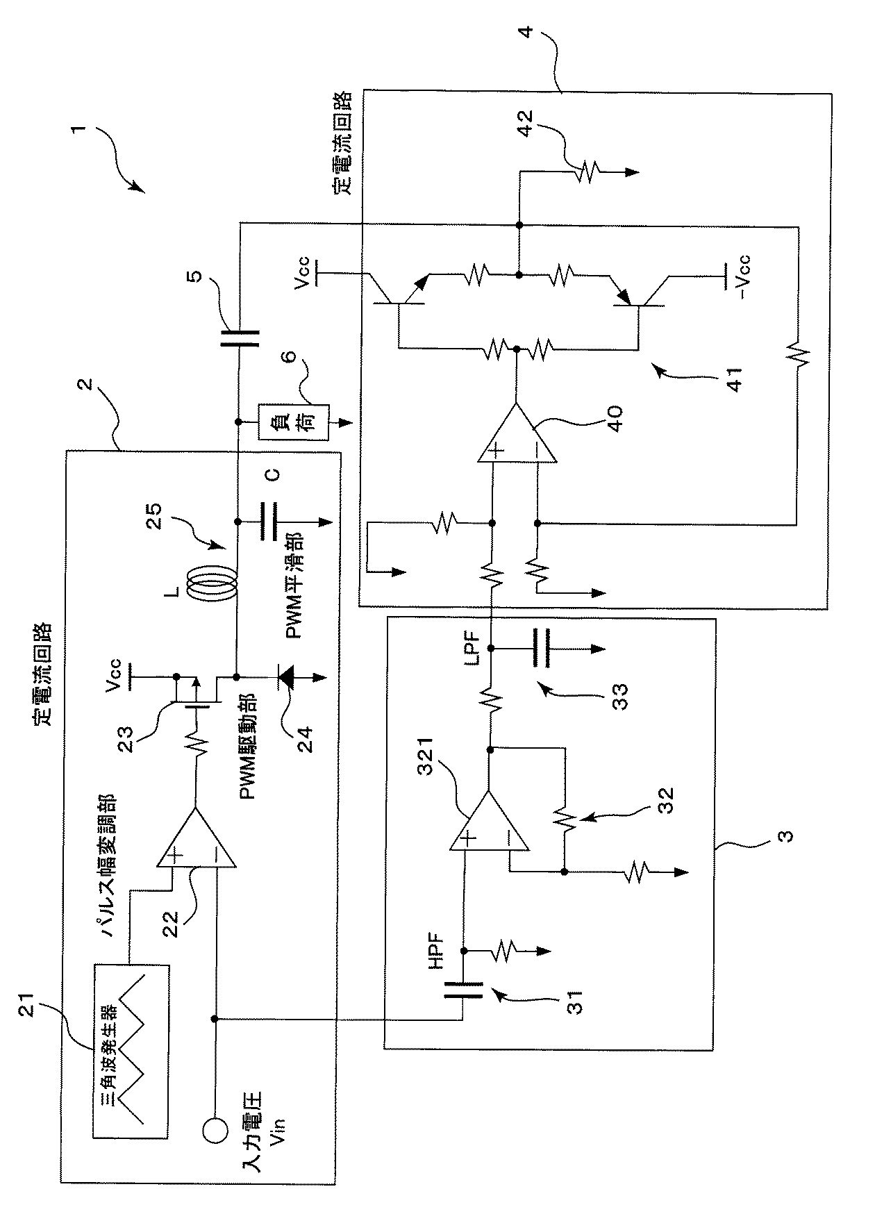
図1は本発明の一実施形態としての広帯域パルス幅変調(PWM)回路の構成を示すブロック図で、この図1に示す広帯域PWM回路1は、パルス幅変調(PWM)回路(定電流回路)2,周波数帯域選択増幅回路3,電流ブースタ回路(定電流回路)4及び加算部(合成回路)5をそなえて構成されている。なお、符号6はこの広帯域PWM回路1の出力電流を受けて駆動される負荷(例えば、半導体レーザ等)を示す。
[A] Description of Embodiment FIG. 1 is a block diagram showing a configuration of a wideband pulse width modulation (PWM) circuit as an embodiment of the present invention. The
ここで、パルス幅変調回路2は、入力信号をパルス幅変調し平滑化して負荷6に電流(I1)を流すもので、例えば、入力信号に応じてパルスの時比率(Duty比)を変化させるパルス幅変調部と、その時比率(Duty比)を有するパルス電圧により駆動されるスイッチング素子(FET等)(PWM駆動部)と、このスイッチング素子から得られた変調電流を平滑化するPWM平滑部(平滑フィルタ)としての機能をそなえて構成される。この平滑フィルタは、コイル(L)とコンデンサ(C)から構成される。このため、パルス幅変調回路2は、一般的に1次あるいは2次の低域通過フィルタ(LPF:Low Pass Filter)の伝達特性を有する。
Here, the pulse
周波数帯域選択増幅回路3は、入力電圧信号の特定周波数帯域、具体的には、PWM回路2自体がもつ伝達特性(周波数特性)を高域側に拡張するのに必要な周波数帯域だけを選択的に増幅するものであり、ここでは、例えば高域通過フィルタ(HPF:High Pass Filter)31,増幅回路32,LPF33により構成され、回路3全体としては帯域通過フィルタ(BPF:Band Pass Filter)の伝達特性を有している。なお、上記HPF31は、パルス幅変調回路2の帯域特性が劣化する周波数から高域の周波数を通過させるフィルタであり、上記LPF33は、増幅回路32の出力のうち上記特定周波数帯域を構成すべき周波数成分のみを通過させて、必要のない高域周波数あるいは制御ループ設計上、排除すべき高域周波数を除去するためのフィルタである。増幅回路32については後述する。
The frequency band
電流ブースタ回路4は、この周波数帯域選択増幅回路3が、通常、オペアンプ等を用いて構成され小電流しか流せない場合が多いため、大電流を供給することを可能とするために電力増幅段としての機能を有する。
合成回路5は、PWM回路2からの電流(I1)と電流ブースタ回路4の出力電流(I2)とを加算(合成)するものである。
In the
The
以上の回路構成により、パルス幅変調回路2の直流から低域までしかない伝達特性を高域の周波数領域まで拡張することができ、過渡変動に高速追従できるようになる。ここで、上述した回路構成の伝達特性(周波数対振幅特性)の一例を図2に示す。この図2において、PWM伝達特性としては次式(1)の2次の遅れ要素を描いている(実線51参照)。これは実際のPWM回路2としてL=10μH、C=22μF、PWM動作周波数100kHzのPWM回路2の伝達特性を模擬している。
With the above circuit configuration, the transfer characteristic of the pulse
なお、この式(1)において、s=jω、K1=1,ω1=2πf1、f1=4kHz、Q1=0.5である。
また、周波数帯域選択増幅回路3のHPF31およびLPF33の伝達関数としては、それぞれ、下記の式(2)および式(3)を用いる。
In this equation (1), s = jω, K 1 = 1, ω 1 = 2πf 1 , f 1 = 4 kHz, and Q 1 = 0.5.
Further, the following equations (2) and (3) are used as the transfer functions of the
ただし、式(2)において、K2=1,ω2=2πf2、f2=100Hz、Q2=0.5であり、式(3)において、K3=1,ω3=2πf3、f3=20kHz、Q3=0.5である。図2においては、実線52がHPF31の伝達特性、実線53がHPF31及びLPF33の合成特性をそれぞれ表している。
なお、この周波数帯域選択増幅回路3の中段に位置する増幅回路32および電流ブースタ回路4はLPF33およびHPF31に内包されるものとして記述していない。これより上述した回路構成(図1参照)によりPWM回路2の信号周波数帯域特性(総合特性:図2の実線54参照)が実効的に高域(領域C)まで拡張されることが分かる。
However, in Equation (2), K 2 = 1, ω 2 = 2πf 2 , f 2 = 100 Hz, Q 2 = 0.5, and in Equation (3), K 3 = 1, ω 3 = 2πf 3 , f 3 = 20 kHz, Q 3 = 0.5. In FIG. 2, the
The
次に、実際の電子回路構成例について説明する。
図3に示すように、パルス幅変調回路2は、前記パルス幅変調部として三角波発生器21及びコンパレータ22、前記PWM駆動部としてトランジスタ(FET)23及びフリーホイールダイオード24、前記PWM平滑部(平滑フィルタ)25としてコイル(L)及びコンデンサ(C)をそなえて構成される。
Next, an actual electronic circuit configuration example will be described.
As shown in FIG. 3, the pulse
ここで、三角波発生器21は、コンパレータ22での比較対象となる三角波を発生するものであり、コンパレータ22は、当該三角波と入力信号電圧(Vin)とを比較することにより例えば図4に示すように入力信号電圧の大小に応じてパルス幅変調波を得るものである。なお、PWM動作における時比率(Duty比)の定義は次式(4)の通りとなる。
Here, the
トランジスタ(スイッチング素子)23は、このコンパレータ22から出力されるパルス幅変調を受けたパルス電圧によりスイッチング動作するものであり、平滑フィルタ25は、このトランジスタ23から供給されるスイッチング電流を平滑化するものであり、フリーホイールダイオード24は、環流電流経路を確保するためのものである。
以上の構成により、パルス幅変調回路2から負荷6に流れる電流ILは、負荷抵抗をRLとして、次式(5)で表される。
The transistor (switching element) 23 performs a switching operation by the pulse voltage subjected to the pulse width modulation output from the
With the above configuration, the current I L flowing from the pulse
一方、周波数帯域選択増幅回路3は、コンデンサ及び抵抗から成るHPF31と、オペアンプ321を用いた増幅回路32と、抵抗及びコンデンサから成るLPF33とにより構成される。
ここで、HPF31は、図2に示したようにPWM回路2で減衰した高域の周波数成分(入力電圧信号の前記特定周波数帯域を構成する高周波数成分)のみを通過させるものであり、増幅回路32は、PWM回路2からの電流と電流ブースタ回路4からの電流とを加算部5としてのコンデンサ5で合成した際に回路全体の通過帯域特性が可能な限り平坦になるようにスケール調整を行なう役割を担うものである。LPF33は、この増幅回路32の出力の不要な高域周波数成分を除去して前記特定周波数帯域を構成する低周波成分のみを通過させるもので、例えば本広帯域PWM回路1を光増幅器等における自動利得制御(AGC)回路に組み込んだ場合に制御ループの遅れ補償を行なう場合に必要となるものである。
On the other hand, the frequency band
Here, as shown in FIG. 2, the
次に、電流ブースタ回路4は、オペアンプ40及びプッシュプル回路41を用いて構成され、通常、周波数帯域選択増幅回路3がオペアンプ321のような数十mA(ミリアンペア)程度の小電流しか流せない構成の場合が多いので、それを補うために数A(アンペア)程度まで流すことができる電力増幅段の機能を実現する。もっとも、前段の周波数帯域選択増幅回路3において十分な電流(数A程度)が得られれば、本電流ブースタ回路4は不要になる。
Next, the
ここで、電流ブースタ回路4と負荷6との接続はコンデンサ5を用いて直流信号を切断した構成にする。こうしないと、PWM回路2を通過した直流信号が電流ブースタ回路4に引きずられためである。つまり、直流から低周波までの領域(図2の領域A)はPWM回路2のみを動作させたいので電流ブースタ回路4からの直流信号は遮断する。
また、抵抗42はコンデンサ5による電荷の充放電を助長する役目を果たす。この抵抗42がないと電流ブースタ回路4が負荷6から電流を吸い込む際にインピーダンスが高くなっているために、立ち上り時間が大きくなる。よって、抵抗42を接続することによりコンデンサ5での変位電流の充放電を助長し負荷電流の立上り及び立下り時間を速くすることができる。
Here, the connection between the
The
以上の構成により、負荷6には、低周波までの領域(図2の領域A:光増幅器に適用する場合は数十kHz程度)ではPWM回路2からの電流が流れ、中域から高域までの領域(図2の領域B)ではPWM回路2および電流ブースタ回路4からの合成電流が流れ、高域(図2の領域C:100〜200kHz程度)では電流ブースタ回路4からの電流が流れることになる。
With the above configuration, the current from the
本広帯域PWM回路1の効果を確認するために、本願発明者は、電子回路シミュレータ(PSpice)によるシミュレーションを行なった。シミュレーションに用いた電子回路図および回路定数を図5に、過渡応答のシミュレーション結果を図6にそれぞれ示す。なお、実線61が入力ステップ電圧波形、実線62がこの入力ステップ電圧波形61に対するPWM回路2のみの場合の過渡応答波形、実線63が入力ステップ電圧波形61に対する本実施形態の広帯域PWM回路1の過渡応答波形をそれぞれ示している。
In order to confirm the effect of the present
このシミュレーション結果から明らかなようにステップ波形の立下りの部分で4〜5倍ほど立下り時間が速くなっている。なお、本回路1では、負荷6への信号経路が2経路あるため、過渡応答波形にオーバーシュートやアンダーシュート、リンギング等が現れないよう、フィルタ31,33の周波数特性や減衰特性及び経路利得を微調整し最適化する必要がある。
As is clear from the simulation results, the fall time is about 4 to 5 times faster at the fall of the step waveform. In this
〔B〕適用例
図7は上述した広帯域PWM回路1を励起光レーザドライバとして適用した構成を示すブロック図で、図8により前述した誤差増幅器700の出力と励起光レーザ1000との間に、本実施形態の広帯域PWM回路1が介装されることにより、EDF100の入力光モニタ信号及び出力光モニタ信号をそれぞれ受光する受光素子500,600の各出力を比較してEDF100の入出力レベル誤差を検出し誤差検出信号を出力する誤差増幅器(誤差検出部)700と、光AGC(自動利得制御)動作の制御ループの安定性と応答速度とを確保するPID(比例・積分・微分器)制御器800としての機能を内包した本実施形態の広帯域PWM回路1とをそなえて成る制御部が構成されている。
[B] Application Example FIG. 7 is a block diagram showing a configuration in which the above-described
即ち、この制御部は、誤差増幅器700の出力(誤差検出信号)を入力電圧信号としてその電圧信号に応じてパルス幅を変調し平滑化して励起光レーザ1000に駆動電流を流すPWM回路2と、上記誤差検出信号の特定周波数帯域だけを選択的に増幅する周波数帯域選択増幅回路3と、その出力電流を増幅する電流ブースタ回路4と、PWM回路2の上記駆動電流と電流ブースタ回路の出力電流とを合成する合成回路5とをそなえて構成される。なお、他の既述の符号と同一符号を付した構成要素は、それぞれ、図8により前述したものと同一若しくは同様のものである。
That is, this control unit uses the output (error detection signal) of the
これにより、この図7に示す光増幅器では、EDF100の入出力側で信号光をPINフォトダイオード等の受光素子500,600によりモニタし、光電力利得が一定になるように励起光レーザ(半導体レーザ)1000を制御する。この際、広帯域PWM回路1によって、EDF100の入出力光レベルが大きく変動したとしても、当該変動に高速に応答して追従することが可能となる。
Accordingly, in the optical amplifier shown in FIG. 7, the signal light is monitored by the
なお、本構成と従来構成(図8参照)とを比較すると、PID制御器800が本構成では削除されていることが分かる。こうすることができる理由は、本回路1の回路構成では、周波数帯域選択増幅回路3による選択周波数帯域を調整する等してその帯域特性を調整することができるので、光AGC(自動利得制御)動作におけるPID(比例・積分・微分器)制御器800としての機能を兼ねることが可能であるからである。また、本例においても、周波数帯域選択増幅回路3において十分な電流(数A程度)が得られれば、電流ブースタ回路4は不要になる。
When this configuration is compared with the conventional configuration (see FIG. 8), it can be seen that the
さらに、本例では、増幅媒体としてEDF100を用いた光増幅器の励起光レーザドライバとして本広帯域PWM回路1を適用した例を示したが、勿論、他の増幅媒体を用いた光増幅器のドライバとしても適用できることはいうまでもなく、さらに、光増幅器に限らず、他の光通信機器における電子冷却素子や電熱ヒーター等の構成物のように大電流が必要とされる場合の消費電力低減のためにも有用である。
Further, in this example, the example in which the present
以上のように、本実施形態によれば、電力効率が良いPWM回路2の長所を維持しつつ、所望の信号帯域特性を有し高速応答が可能な回路が容易に実現できるので、特に近年、低消費電力化の要求と高速応答性の要求が強くなってきている光増幅器の分野において、これらの要求の両立を実現することが可能となる。
なお、本発明は、上述した実施形態に限定されず、本発明の趣旨を逸脱しない範囲で種々変形して実施できることはいうまでもない。
As described above, according to the present embodiment, it is possible to easily realize a circuit having desired signal bandwidth characteristics and capable of high-speed response while maintaining the advantages of the
Needless to say, the present invention is not limited to the above-described embodiments, and various modifications can be made without departing from the spirit of the present invention.
〔C〕付記
(付記1)
入力電圧信号に応じてパルス幅を変調し平滑化して負荷に電流を流すパルス幅変調回路と、
該入力電圧信号の特定周波数帯域だけを選択的に増幅する周波数帯域選択増幅回路と、
該パルス幅変調回路の該電流と該周波数帯域選択増幅回路による増幅後の電流とを合成する合成回路とをそなえて構成されたことを特徴とする、広帯域パルス幅変調回路。
[C] Appendix (Appendix 1)
A pulse width modulation circuit that modulates and smoothes the pulse width according to the input voltage signal and flows current to the load; and
A frequency band selective amplifier circuit that selectively amplifies only a specific frequency band of the input voltage signal;
A wideband pulse width modulation circuit comprising: a synthesis circuit that synthesizes the current of the pulse width modulation circuit and the current amplified by the frequency band selection amplification circuit.
(付記2)
入力電圧信号に応じてパルス幅を変調し平滑化して負荷に電流を流すパルス幅変調回路と、
該入力電圧信号の特定周波数帯域だけを選択的に増幅する周波数帯域選択増幅回路と、
該周波数帯域選択増幅回路の出力電流を増幅する電流ブースタ回路と、
該パルス幅変調回路の該電流と電流ブースタ回路の出力電流とを合成する合成回路とをそなえて構成されたことを特徴とする、広帯域パルス幅変調回路。
(Appendix 2)
A pulse width modulation circuit that modulates and smoothes the pulse width according to the input voltage signal and flows current to the load; and
A frequency band selective amplifier circuit that selectively amplifies only a specific frequency band of the input voltage signal;
A current booster circuit for amplifying the output current of the frequency band selective amplifier circuit;
A wide-band pulse width modulation circuit comprising a synthesis circuit that synthesizes the current of the pulse width modulation circuit and the output current of a current booster circuit.
(付記3)
該負荷が半導体レーザであることを特徴とする、付記1又は2に記載の広帯域パルス幅変調回路。
(付記4)
該合成回路が、直流信号を遮断するコンデンサにより構成されたことを特徴とする、付記1〜3のいずれか1項に記載の広帯域パルス幅変調回路。
(Appendix 3)
The broadband pulse width modulation circuit according to
(Appendix 4)
4. The broadband pulse width modulation circuit according to any one of
(付記5)
該周波数帯域選択増幅回路が、
該パルス幅変調回路の周波数帯域特性が劣化する周波数から高域の周波数を通過させる高域通過フィルタと、
該高域通過フィルタの出力を増幅して該特定周波数帯域の通過帯域特性が平坦になるようスケール調整を行なう増幅器と、
該増幅器の出力のうち該特定周波数帯域を構成すべき周波数成分のみを通過させる低域通過フィルタとをそなえて構成されたことを特徴とする、付記1〜4のいずれか1項に記載の広帯域パルス幅変調回路。
(Appendix 5)
The frequency band selective amplifier circuit is
A high-pass filter that passes a high frequency from a frequency at which the frequency band characteristics of the pulse width modulation circuit deteriorate;
An amplifier for amplifying the output of the high-pass filter and adjusting the scale so that the passband characteristic of the specific frequency band becomes flat;
The wideband according to any one of
(付記6)
半導体レーザと、
該半導体レーザの出力を励起光として入力光信号の増幅を行なう光増幅媒体と、
該光増幅媒体の入出力レベル誤差を検出する誤差検出部と、
該誤差検出部による誤差検出信号を入力電圧信号としてその電圧信号に応じてパルス幅を変調し平滑化して該半導体レーザに駆動電流を流すパルス幅変調回路と、該入力電圧信号の特定周波数帯域だけを選択的に増幅する周波数帯域選択増幅回路と、該パルス幅変調回路の該駆動電流と該周波数帯域選択増幅回路による増幅後の電流とを合成する合成回路とを有する広帯域パルス変調回路とをそなえたことを特徴とする、光増幅器。
(Appendix 6)
A semiconductor laser;
An optical amplification medium that amplifies an input optical signal using the output of the semiconductor laser as excitation light;
An error detection unit for detecting an input / output level error of the optical amplification medium;
An error detection signal from the error detection unit as an input voltage signal, a pulse width modulation circuit for modulating and smoothing the pulse width according to the voltage signal and flowing a drive current to the semiconductor laser, and a specific frequency band of the input voltage signal And a wideband pulse modulation circuit comprising: a frequency band selective amplifier circuit that selectively amplifies the signal; and a synthesis circuit that combines the drive current of the pulse width modulation circuit and the current amplified by the frequency band selective amplifier circuit. An optical amplifier characterized by that.
(付記7)
半導体レーザと、
該半導体レーザの出力を励起光として入力光信号の増幅を行なう光増幅媒体と、
該光増幅媒体の入出力レベル誤差を検出する誤差検出部と、
該誤差検出部による誤差検出信号を入力電圧信号としてその電圧信号に応じてパルス幅を変調し平滑化して該半導体レーザに駆動電流を流すパルス幅変調回路と、該入力電圧信号の特定周波数帯域だけを選択的に増幅する周波数帯域選択増幅回路と、該周波数帯域選択増幅回路の出力電流を増幅する電流ブースタ回路と、該パルス幅変調回路の該駆動電流と該電流ブースタ回路の出力電流とを合成する合成回路とを有する広帯域パルス変調回路とをそなえたことを特徴とする、光増幅器。
(Appendix 7)
A semiconductor laser;
An optical amplification medium that amplifies an input optical signal using the output of the semiconductor laser as excitation light;
An error detection unit for detecting an input / output level error of the optical amplification medium;
An error detection signal from the error detection unit as an input voltage signal, a pulse width modulation circuit for modulating and smoothing the pulse width according to the voltage signal and flowing a drive current to the semiconductor laser, and a specific frequency band of the input voltage signal A frequency band selective amplifier circuit that selectively amplifies the current, a current booster circuit that amplifies the output current of the frequency band selective amplifier circuit, the drive current of the pulse width modulation circuit, and the output current of the current booster circuit An optical amplifier comprising: a wideband pulse modulation circuit having a combining circuit.
(付記8)
該合成回路が、直流信号を遮断するコンデンサにより構成されたことを特徴とする、付記6又は7に記載の光増幅器。
(付記9)
該周波数帯域選択増幅回路が、
該入力電圧信号の該特定周波数帯域を構成する高周波数成分のみを通過させる高域通過フィルタと、
該高域通過フィルタの出力を増幅して該特定周波数帯域の通過帯域特性が平坦になるようスケール調整を行なう増幅器と、
該増幅器の出力の該特定周波数帯域を構成する低周波成分のみを通過させる低域通過フィルタとをそなえて構成されたことを特徴とする、付記6〜8のいずれか1項に記載の光増幅器。
(Appendix 8)
8. The optical amplifier according to
(Appendix 9)
The frequency band selective amplifier circuit is
A high-pass filter that passes only high-frequency components constituting the specific frequency band of the input voltage signal;
An amplifier for amplifying the output of the high-pass filter and adjusting the scale so that the passband characteristic of the specific frequency band becomes flat;
The optical amplifier according to any one of appendices 6 to 8, further comprising a low-pass filter that passes only a low-frequency component constituting the specific frequency band of the output of the amplifier. .
以上詳述したように、本発明によれば、入力電圧信号の特定周波数帯域だけを選択的に増幅し、これをパルス幅変調回路の電流と合成するので、電力効率が良いパルス幅変調の長所を維持しつつ、高速応答が可能な回路が実現でき、特に近年、低消費電力化の要求と高速応答性の要求が強くなってきている光増幅器等光通信分野において極めて有用と考えられる。 As described above in detail, according to the present invention, only a specific frequency band of the input voltage signal is selectively amplified and synthesized with the current of the pulse width modulation circuit. Thus, it is possible to realize a circuit capable of high-speed response while maintaining the above, and in particular, it is considered to be extremely useful in the optical communication field such as an optical amplifier, in which demands for low power consumption and high-speed response are increasing in recent years.
1 広帯域パルス幅変調(PWM)回路
2 パルス幅変調(PWM)回路(定電流回路)
21 三角波発生器
22 コンパレータ
23 トランジスタ(FET)
24 フリーホイールダイオード
25 平滑回路(平滑フィルタ)
L コイル
C コンデンサ
3 周波数帯域選択増幅回路
31 高域通過フィルタ(HPF)
32 増幅回路
321 オペアンプ
33 低域通過フィルタ(LPF)
4 電流ブースタ回路(定電流回路)
40 オペアンプ
41 プッシュプル回路
42 抵抗
5 加算部(合成回路)
6 負荷(半導体レーザ)
100 エルビウム添加光ファイバ(EDF)
200,300,400 光カプラ
500,600 受光素子
700 誤差増幅器
1000 励起光レーザ(半導体レーザ)
1 Broadband pulse width modulation (PWM)
21
24
L
32
4 Current booster circuit (constant current circuit)
40
6 Load (semiconductor laser)
100 Erbium-doped optical fiber (EDF)
200, 300, 400
Claims (5)
該入力電圧信号の該パルス幅変調回路の帯域特性が劣化する周波数から高域の周波数だけを選択的に増幅する周波数帯域選択増幅回路と、
該パルス幅変調回路の該電流と該周波数帯域選択増幅回路による増幅後の電流とを合成する合成回路とをそなえて構成されたことを特徴とする、広帯域パルス幅変調回路。 A pulse width modulation circuit that modulates and smoothes the pulse width according to the input voltage signal and flows current to the load; and
A frequency band selective amplifier circuit that selectively amplifies only the high frequency from the frequency at which the band characteristics of the pulse width modulation circuit of the input voltage signal deteriorate ;
A wideband pulse width modulation circuit comprising: a synthesis circuit that synthesizes the current of the pulse width modulation circuit and the current amplified by the frequency band selection amplification circuit.
該入力電圧信号の該パルス幅変調回路の帯域特性が劣化する周波数から高域の周波数だけを選択的に増幅する周波数帯域選択増幅回路と、
該周波数帯域選択増幅回路の出力電流を増幅する電流ブースタ回路と、
該パルス幅変調回路の該電流と電流ブースタ回路の出力電流とを合成する合成回路とをそなえて構成されたことを特徴とする、広帯域パルス幅変調回路。 A pulse width modulation circuit that modulates and smoothes the pulse width according to the input voltage signal and flows current to the load; and
A frequency band selective amplifier circuit that selectively amplifies only the high frequency from the frequency at which the band characteristics of the pulse width modulation circuit of the input voltage signal deteriorate ;
A current booster circuit for amplifying the output current of the frequency band selective amplifier circuit;
A wide-band pulse width modulation circuit comprising a synthesis circuit that synthesizes the current of the pulse width modulation circuit and the output current of a current booster circuit.
該半導体レーザの出力を励起光として入力光信号の増幅を行なう光増幅媒体と、
該光増幅媒体の入出力レベル誤差を検出する誤差検出部と、
該誤差検出部による誤差検出信号を入力電圧信号としてその電圧信号に応じてパルス幅を変調し平滑化して該半導体レーザに駆動電流を流すパルス幅変調回路と、該入力電圧信号の該パルス幅変調回路の帯域特性が劣化する周波数から高域の周波数だけを選択的に増幅する周波数帯域選択増幅回路と、該パルス幅変調回路の該駆動電流と該周波数帯域選択増幅回路による増幅後の電流とを合成する合成回路とを有する広帯域パルス変調回路とをそなえたことを特徴とする、光増幅器。 A semiconductor laser;
An optical amplification medium that amplifies an input optical signal using the output of the semiconductor laser as excitation light;
An error detection unit for detecting an input / output level error of the optical amplification medium;
A pulse width modulation circuit that modulates and smoothes a pulse width according to the voltage detection signal using an error detection signal from the error detection unit as an input voltage signal, and sends a drive current to the semiconductor laser, and the pulse width modulation of the input voltage signal A frequency band selective amplifier circuit that selectively amplifies only a high frequency from a frequency at which the band characteristics of the circuit deteriorate , and the driving current of the pulse width modulation circuit and the current amplified by the frequency band selective amplifier circuit What is claimed is: 1. An optical amplifier comprising a broadband pulse modulation circuit having a synthesis circuit for synthesis.
該半導体レーザの出力を励起光として入力光信号の増幅を行なう光増幅媒体と、
該光増幅媒体の入出力レベル誤差を検出する誤差検出部と、
該誤差検出部による誤差検出信号を入力電圧信号としてその電圧信号に応じてパルス幅を変調し平滑化して該半導体レーザに駆動電流を流すパルス幅変調回路と、該入力電圧信号の該パルス幅変調回路の帯域特性が劣化する周波数から高域の周波数だけを選択的に増幅する周波数帯域選択増幅回路と、該周波数帯域選択増幅回路の出力電流を増幅する電流ブースタ回路と、該パルス幅変調回路の該駆動電流と該電流ブースタ回路の出力電流とを合成する合成回路とを有する広帯域パルス変調回路とをそなえたことを特徴とする、光増幅器。 A semiconductor laser;
An optical amplification medium that amplifies an input optical signal using the output of the semiconductor laser as excitation light;
An error detection unit for detecting an input / output level error of the optical amplification medium;
A pulse width modulation circuit that modulates and smoothes a pulse width according to the voltage detection signal using an error detection signal from the error detection unit as an input voltage signal, and sends a drive current to the semiconductor laser, and the pulse width modulation of the input voltage signal A frequency band selective amplifier circuit that selectively amplifies only a high frequency from a frequency at which the band characteristics of the circuit deteriorate, a current booster circuit that amplifies an output current of the frequency band selective amplifier circuit, and a pulse width modulation circuit An optical amplifier comprising: a broadband pulse modulation circuit having a synthesis circuit for synthesizing the drive current and the output current of the current booster circuit.
Priority Applications (2)
| Application Number | Priority Date | Filing Date | Title |
|---|---|---|---|
| JP2004004271A JP4448700B2 (en) | 2004-01-09 | 2004-01-09 | Broadband pulse width modulation circuit and optical amplifier using the same |
| US10/836,233 US7187872B2 (en) | 2004-01-09 | 2004-05-03 | Broadband pulse width modulation circuit and optical amplifier using the same |
Applications Claiming Priority (1)
| Application Number | Priority Date | Filing Date | Title |
|---|---|---|---|
| JP2004004271A JP4448700B2 (en) | 2004-01-09 | 2004-01-09 | Broadband pulse width modulation circuit and optical amplifier using the same |
Publications (2)
| Publication Number | Publication Date |
|---|---|
| JP2005197590A JP2005197590A (en) | 2005-07-21 |
| JP4448700B2 true JP4448700B2 (en) | 2010-04-14 |
Family
ID=34737188
Family Applications (1)
| Application Number | Title | Priority Date | Filing Date |
|---|---|---|---|
| JP2004004271A Expired - Fee Related JP4448700B2 (en) | 2004-01-09 | 2004-01-09 | Broadband pulse width modulation circuit and optical amplifier using the same |
Country Status (2)
| Country | Link |
|---|---|
| US (1) | US7187872B2 (en) |
| JP (1) | JP4448700B2 (en) |
Families Citing this family (9)
| Publication number | Priority date | Publication date | Assignee | Title |
|---|---|---|---|---|
| US20060140644A1 (en) * | 2004-12-23 | 2006-06-29 | Paolella Arthur C | High performance, high efficiency fiber optic link for analog and RF systems |
| JP2008016561A (en) * | 2006-07-04 | 2008-01-24 | Produce:Kk | Rapid discharging method by dropping voltage of capacitor |
| US20080137179A1 (en) * | 2006-12-08 | 2008-06-12 | General Instrument Corporation | Method and Apparatus for Controlling an Optical Amplifier for Use in a Passive Optical Network |
| US7773669B2 (en) * | 2007-08-10 | 2010-08-10 | Intel Corporation | Cascaded phase pulse position and pulse width modulation based digital transmitter |
| WO2009037603A2 (en) * | 2007-08-16 | 2009-03-26 | St-Nxp Wireless (Holding) Ag | Polar modulation based transmitter with switching mode power amplifiers |
| JP2015076581A (en) * | 2013-10-11 | 2015-04-20 | ソニー株式会社 | Optical transmission circuit, optical transmission device, and optical transmission system |
| CN104200041B (en) * | 2014-09-17 | 2017-01-25 | 电子科技大学 | Rapid extraction method of broadband characteristic modes |
| US10602940B1 (en) * | 2018-11-20 | 2020-03-31 | Genetesis, Inc. | Systems, devices, software, and methods for diagnosis of cardiac ischemia and coronary artery disease |
| CN110336618A (en) * | 2019-06-17 | 2019-10-15 | 武汉永信丰科技有限公司 | A kind of optical module control method, device and storage medium |
Family Cites Families (4)
| Publication number | Priority date | Publication date | Assignee | Title |
|---|---|---|---|---|
| JP2830619B2 (en) | 1992-05-29 | 1998-12-02 | 日新電機株式会社 | Static var compensator |
| US5448629A (en) * | 1993-10-14 | 1995-09-05 | At&T Corp. | Amplitude detection scheme for optical transmitter control |
| US5450383A (en) | 1994-05-26 | 1995-09-12 | International Business Machines Corporation | Monitoring and adjusting laser write power in an optical disk recorder using pulse-width modulated power level checking signals |
| US6330279B1 (en) * | 1998-02-06 | 2001-12-11 | Seagate Technology Llc | System and method of correcting gain and offset error in a signal amplifier for a position sensitive detector |
-
2004
- 2004-01-09 JP JP2004004271A patent/JP4448700B2/en not_active Expired - Fee Related
- 2004-05-03 US US10/836,233 patent/US7187872B2/en active Active
Also Published As
| Publication number | Publication date |
|---|---|
| US7187872B2 (en) | 2007-03-06 |
| US20050152703A1 (en) | 2005-07-14 |
| JP2005197590A (en) | 2005-07-21 |
Similar Documents
| Publication | Publication Date | Title |
|---|---|---|
| US6984969B1 (en) | High efficiency high speed low noise regulator | |
| US9252724B2 (en) | 2G support for 2G and 3G/4G envelope tracking modulator | |
| US8030995B2 (en) | Power circuit used for an amplifier | |
| US7671675B2 (en) | Output limiting circuit, class D power amplifier and audio equipment | |
| JP4448700B2 (en) | Broadband pulse width modulation circuit and optical amplifier using the same | |
| JP6452622B2 (en) | Envelope tracking modulator with feedback | |
| EP2395655A1 (en) | Power amplifier and power amplification method | |
| JP6210027B2 (en) | Power amplifier | |
| WO2009104746A1 (en) | Modulation method, modulation program, recording medium, modulation device, and light transmitter | |
| KR20150118171A (en) | Improved voltage boost for et modulator | |
| JP2005102146A (en) | Amplifier, and high frequency power amplifier using the same | |
| US20050238072A1 (en) | Laser driver circuit | |
| JP2007305762A (en) | Drive circuit of laser diode | |
| KR20150129762A (en) | Switching power converter | |
| US20040052281A1 (en) | Laser device, controller and method for controlling the laser device | |
| JP2010518708A (en) | Method and system for increasing the sampling frequency of a switching amplifier | |
| US7345540B2 (en) | Amplifier circuit having a compensating amplifier unit for improving loop gain and linearity | |
| US6778570B2 (en) | Laser driving apparatus and method | |
| US20080204132A1 (en) | Class-D Amplifier | |
| JP4710870B2 (en) | Digital amplifier device and speaker device | |
| US20090039856A1 (en) | Stability enhancement apparatus and method for a self-clocking PWM buck converter | |
| JP3413281B2 (en) | Power amplifier circuit | |
| CN115244949A (en) | Sound equipment | |
| US20120044019A1 (en) | Power amplifier | |
| CN208638335U (en) | A kind of feedback regulation jump pulse protective device suitable for PWM power amplifier |
Legal Events
| Date | Code | Title | Description |
|---|---|---|---|
| A621 | Written request for application examination |
Free format text: JAPANESE INTERMEDIATE CODE: A621 Effective date: 20061208 |
|
| A131 | Notification of reasons for refusal |
Free format text: JAPANESE INTERMEDIATE CODE: A131 Effective date: 20090630 |
|
| A521 | Written amendment |
Free format text: JAPANESE INTERMEDIATE CODE: A523 Effective date: 20090825 |
|
| TRDD | Decision of grant or rejection written | ||
| A01 | Written decision to grant a patent or to grant a registration (utility model) |
Free format text: JAPANESE INTERMEDIATE CODE: A01 Effective date: 20100105 |
|
| A01 | Written decision to grant a patent or to grant a registration (utility model) |
Free format text: JAPANESE INTERMEDIATE CODE: A01 |
|
| A61 | First payment of annual fees (during grant procedure) |
Free format text: JAPANESE INTERMEDIATE CODE: A61 Effective date: 20100125 |
|
| FPAY | Renewal fee payment (event date is renewal date of database) |
Free format text: PAYMENT UNTIL: 20130129 Year of fee payment: 3 |
|
| R150 | Certificate of patent or registration of utility model |
Ref document number: 4448700 Country of ref document: JP Free format text: JAPANESE INTERMEDIATE CODE: R150 Free format text: JAPANESE INTERMEDIATE CODE: R150 |
|
| FPAY | Renewal fee payment (event date is renewal date of database) |
Free format text: PAYMENT UNTIL: 20130129 Year of fee payment: 3 |
|
| FPAY | Renewal fee payment (event date is renewal date of database) |
Free format text: PAYMENT UNTIL: 20140129 Year of fee payment: 4 |
|
| LAPS | Cancellation because of no payment of annual fees |