JP4447963B2 - Optical deflector control device - Google Patents
Optical deflector control device Download PDFInfo
- Publication number
- JP4447963B2 JP4447963B2 JP2004162536A JP2004162536A JP4447963B2 JP 4447963 B2 JP4447963 B2 JP 4447963B2 JP 2004162536 A JP2004162536 A JP 2004162536A JP 2004162536 A JP2004162536 A JP 2004162536A JP 4447963 B2 JP4447963 B2 JP 4447963B2
- Authority
- JP
- Japan
- Prior art keywords
- optical deflector
- frequency
- light
- control device
- optical
- Prior art date
- Legal status (The legal status is an assumption and is not a legal conclusion. Google has not performed a legal analysis and makes no representation as to the accuracy of the status listed.)
- Expired - Fee Related
Links
Images


Description
本発明は、光偏向器、及び光偏向器を制御する光偏向器制御装置、更にはそれを用いた画像形成装置などに関する。例えば、光の偏向走査によって画像を投影するプロジェクションディスプレイや、電子写真プロセスを有するレーザービームプリンタ、デジタル複写機等の画像形成装置に好適なものである。 The present invention relates to an optical deflector, an optical deflector control device that controls the optical deflector, and an image forming apparatus using the optical deflector control device. For example, it is suitable for an image forming apparatus such as a projection display for projecting an image by light deflection scanning, a laser beam printer having an electrophotographic process, a digital copying machine or the like.
従来から、光偏向器として正弦振動を行う光偏向器を使用した光走査系が種々と提案されている。正弦振動を行う光偏向器を使用した光走査系は、ポリゴンミラー等の回転多面鏡を使用した光走査光学系に比べて、光偏向器を大幅に小型化することが可能であること、消費電力が少ないこと、特に半導体プロセスによって製造されるSi単結晶からなる光偏向器は理論上金属疲労が無く耐久性にも優れていること等の特徴がある。 Conventionally, various optical scanning systems using an optical deflector that performs sinusoidal vibration as an optical deflector have been proposed. Compared with optical scanning optical systems using rotating polygonal mirrors such as polygon mirrors, the optical scanning system using optical deflectors that perform sinusoidal vibration can significantly reduce the size of the optical deflector. An optical deflector made of a Si single crystal manufactured by a semiconductor process, in particular, has characteristics such as theoretically no metal fatigue and excellent durability.
一方、正弦振動を行う光偏向器によって反射偏向された光は、回転多面鏡を使用した光偏向器に比べ、偏向走査の角速度が一定とならず余弦的に変化する。特に偏向走査の両端に向かうにつれ偏向走査の角速度は減少するため、被走査面上で等速走査が必要な応用には、結像光学系(結像レンズ)としてarcsinレンズを用いることが多い。arcsinレンズを用いる場合、走査中心に対して走査端部の主走査方向のFナンバーが変化してしまうという特性があり、走査中心と走査端部との被走査面上におけるスポット径が不均一になってしまう。 On the other hand, the light reflected and deflected by the optical deflector that performs sinusoidal vibration has a cosine change because the angular velocity of the deflection scan is not constant as compared with the optical deflector that uses a rotating polygon mirror. In particular, since the angular velocity of deflection scanning decreases toward both ends of deflection scanning, an arcsin lens is often used as an imaging optical system (imaging lens) for applications that require constant speed scanning on the surface to be scanned. When an arcsin lens is used, there is a characteristic that the F number in the main scanning direction of the scanning end changes with respect to the scanning center, and the spot diameter on the surface to be scanned between the scanning center and the scanning end is nonuniform. turn into.
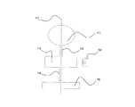
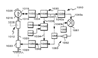
以上のような課題を改善するため、提案がなされている(特許文献1、特許文献2参照)。図11は、特許文献1に開示された光走査系を示す概略図である。光偏向器1012は、第1可動子1014、第2可動子1016とそれらを連結して弾性支持する第1ねじりバネ1018、第2可動子1016と機械的な接地面を弾性支持する第2ねじりバネ1020で構成されている。これら全ての要素は、ねじり軸1026を中心として駆動手段1023によりねじり振動する。また、第1可動子1014は、光を偏向するための反射面を有しており、第1可動子1014のねじり振動によって、光源からの光を偏向走査する。光偏向器1012は、ねじり軸1026を中心としたねじり振動について、基準周波数となる1次の固有振動モードと基準周波数の略3倍の周波数となる2次の固有振動モードを有している。駆動手段1023は、この1次の固有振動モードの周波数とこれに対して同位相で3倍の周波数の2つの周波数で光偏向器1012を駆動する。したがって、光偏向器1012は、1次の固有振動モードに加えて、2次の固有振動モードで同時にねじり振動しているため、第1可動子1014で反射された光の偏向走査の変位角は、この2つの振動モードの重ね合わせとなり、正弦波ではなく略三角波状に変化する。したがって、偏向走査の角速度は、変位角が正弦波であったときと比べ、略等角速度となる領域が広く存在するため、偏向走査の全域に対する利用可能な領域を大きくすることができる。
In order to improve the above problems, proposals have been made (see
一方、第1可動子1014は、偏向走査の反射面の裏面に、変位検出用反射面1015を有している。変位検出手段1032は光を変位検出用反射面1015に入射し、反射光を検出することによって、第1可動子1014の変位角を検出する。変位の検出信号は信号線1034を経て、バンドパスフィルター回路1036で1次の固有振動モードの周波数成分のみ、第1信号線1038、第2信号線1040に送られる。第1信号線1038からの信号は、乗算器1042へ送られ、ここで元の3倍の周波数信号へと変換される。更に、乗算器1042は、位相調節入力1054と振幅調節入力1055を有している。これら2つの入力によって、変位検出手段1032によって検出された第1可動子1014の偏向走査の変位が、適切な略三角波状の変位となるように、乗算器1042からの出力信号の位相、最大振幅をそれぞれ調節することができる。
On the other hand, the
乗算器1042からの信号は、加算器1046へ入力される。加算器1046は、乗算器1042からの信号と、第2信号線1040、自動ゲイン制御回路1060を経た1次の固有振動モードの周波数信号とを加算し、光偏向器1012の駆動信号を生成する。駆動信号は、信号線1048を経て駆動回路1050へ送られ、駆動手段1023を1次の固有振動モードとその3倍の周波数信号の合成波形で駆動する。
A signal from the
自動ゲイン制御回路1060は、ピーク検出回路1056、差分増幅回路1061、プリセット振幅1063、増幅器1062、ゲイン制御回路1064から成る。第2信号線1040は2つの信号線1040a、1040bに分岐される。信号線1040aからの信号は、ピーク検出回路1056で検出された最大振幅と予め設定された振幅値であるプリセット振幅1063との差分を差分増幅回路1061により検出する。この差分信号は、ゲイン制御回路1064を制御する増幅器1062に送られ、信号線1040bからの信号をプリセット振幅1063と同ゲインとなるようにゲイン制御回路1064を制御する。
しかしながら、上記従来例においては、2つの異なる固有振動モードで駆動する際の各周波数成分の重ね合わせの係数(つまり、各周波数成分の振幅の最大値)は、振幅調節入力1055とプリセット振幅1063での既定値によって決定されており、好適な値を設定することが困難であった。
However, in the above conventional example, the superposition coefficient of each frequency component (that is, the maximum value of the amplitude of each frequency component) when driving in two different natural vibration modes is determined by the
上記課題に鑑み、本発明の光偏向器制御装置は、一方の周波数が他方の周波数の定数倍である比例関係にある互いに異なる周波数の正弦振動を行う2つの偏向反射面と、2つの該偏向反射面を駆動する駆動手段と、周波数検知回路と、を有し、2つの前記偏向反射面の正弦振動の重ね合わせにより光源からの光を偏向走査する光偏向器を制御する光偏向器制御装置であって、前記光偏向器によって偏向走査される光の偏向走査の角速度のプリセットされた最大値と最小値および前記周波数検知回路から出力される前記互いに異なる周波数の正弦振動のいずれか1つの周波数から、2つの前記偏向反射面の正弦振動の最大振幅の制御目標値を決定する演算回路を有することを特徴とする。また、本発明の光偏向器制御装置は、偏向反射面を持つ可動子を含む2つ以上の可動子と、該可動子を連結する複数の弾性支持部と、該複数の弾性支持部の一部を支持する支持体で構成されて前記偏向反射面を一振動軸の回りに振動可能にするように構成された振動系と、周波数検知回路と、振動系の有する一方の周波数が他方の周波数の定数倍である比例関係にある2つの異なる固有振動モードで振動系を駆動する駆動手段と、を有し、光源からの光を偏向走査する光偏向器を制御する光偏向器制御装置であって、前記光偏向器によって偏向走査される光の偏向走査の角速度のプリセットされた最大値と最小値および前記周波数検知回路から出力される前記2つの異なる固有振動モードのいずれか1つの周波数から、前記偏向反射面の2つの固有振動モードの最大振幅の制御目標値を決定する演算回路を有することを特徴とする。 In view of the above problems, the optical deflector control device according to the present invention includes two deflecting reflecting surfaces that perform sinusoidal vibrations of different frequencies and in a proportional relationship in which one frequency is a constant multiple of the other frequency, and the two deflecting devices. An optical deflector control device for controlling an optical deflector that deflects and scans light from a light source by superimposing sinusoidal vibrations of the two deflection reflective surfaces , and having a driving means for driving the reflective surface and a frequency detection circuit a is any one of the frequencies of the sinusoidal oscillation of the different frequencies output from the optical deflector angular velocity of the preset deflection scanning of the light that will be deflected and scanned by the maximum value and the minimum value and the frequency detecting circuit To an arithmetic circuit for determining a control target value of the maximum amplitude of sinusoidal vibration of the two deflecting reflecting surfaces. The optical deflector control device according to the present invention includes two or more movers including a mover having a deflecting reflection surface, a plurality of elastic support portions connecting the movers, and one of the plurality of elastic support portions. A vibration system configured by a support body that supports the unit and configured to allow the deflection reflection surface to vibrate around one vibration axis, a frequency detection circuit, and one frequency of the vibration system is the other frequency An optical deflector control device for controlling an optical deflector for deflecting and scanning light from a light source. Te, from any one frequency of the two different natural oscillation modes to be outputted from the preset maximum value and the minimum value and the frequency detection circuit of the angular velocity of the deflection scan of the deflecting scanned Ru light by the optical deflector, two of the deflection reflective surface And having a computation circuit for determining the control target value of the maximum amplitude of natural vibration modes.
また、上記課題に鑑み、本発明の画像表示装置は、光源と、光偏向器と、請求項1乃至4の何れか1つに記載の光偏向器制御装置とを有し、光偏向器は、光偏向器制御装置で制御され、光源からの光を光偏向器により偏向し、該光の少なくとも一部を画像表示体上に投影することを特徴とする。
In view of the above problems, an image display device of the present invention includes a light source, an optical deflector, and the optical deflector control device according to any one of
また、上記課題に鑑み、本発明の画像形成装置は、光源と、光偏向器と、請求項1乃至4の何れか1つに記載の光偏向器制御装置と、感光体とを有し、光偏向器は、光偏向器制御装置で制御され、光源からの光を光偏向器により偏向し、該光の少なくとも一部を感光体上に入射することを特徴とする。
In view of the above problems, an image forming apparatus of the present invention includes a light source, an optical deflector, the optical deflector control device according to any one of
本発明による上記光偏向器制御装置によって、偏向走査の仕様である偏向走査の最大角速度と最小角速度、周波数から、好適な各周波数成分の重ね合わせの係数を決定することが可能となり、所望の領域において偏向走査の角速度が略一定となる構成を実現することができる。 The optical deflector control device according to the present invention makes it possible to determine a suitable superposition coefficient of each frequency component from the maximum angular velocity, the minimum angular velocity, and the frequency of deflection scanning, which are the specifications of deflection scanning, in a desired region. Thus, it is possible to realize a configuration in which the angular velocity of deflection scanning is substantially constant.
以下、本発明の実施例について図面を参照しながら詳細に説明する。
(実施例1)
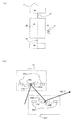
図1は本発明の光偏向器制御装置を含む光走査系の実施例を示すブロック図である。図1に示すように、本実施例の光走査系は、光偏向器31、変位角検知手段32、光偏向器制御装置51で構成される。図2には、光偏向器31の上面図を示した。図示のように、光偏向器31は、第1可動子11、第2可動子13とそれらを連結して弾性支持する第1ねじりバネ(弾性支持部)12、第2可動子13と機械的な支持体15を弾性支持する第2ねじりバネ(弾性支持部)14で構成されている。これら全ての要素(本発明では振動系と呼ぶ)は、ねじりバネ12、14で規定される1つのねじり軸17を中心として駆動手段16によりねじり振動される。また、第1可動子11は、光を偏向するための図示しない反射面を有しており、第1可動子11のねじり振動によって、反射面は光源からの光を偏向走査する。図2では、ねじりバネ12、14を直列的に設けているが、可動子と弾性支持部との連結の仕方、配置は、光偏向面について後記の式3の振動が或る振動軸の回りで起こるのであれば、どの様なものでもよい。
Hereinafter, embodiments of the present invention will be described in detail with reference to the drawings.
Example 1
FIG. 1 is a block diagram showing an embodiment of an optical scanning system including an optical deflector control device of the present invention. As shown in FIG. 1, the optical scanning system of this embodiment includes an
光偏向器31は、ねじり軸17を中心としたねじり振動について、基準周波数となる周波数f0の1次の固有振動モードと基準周波数の2倍の周波数となる2次の固有振動モードを有している2自由度振動系として扱うことができる。駆動手段16は、この1次の固有振動モードの周波数とこれに対して同位相で2倍の周波数の2つの周波数で光偏向器31を駆動する。こうした振動系は、ばね定数、質量、形状などを適当に設計することで構成できる。
The
図3は、横軸を時間tとして、第1可動子11の周波数f0のねじり振動の変位角を説明する図である(本明細書においては、可動子の往復振動の変位角と、光偏向器によって偏向走査される光の変位角とは定数分が異なるのみであるので、等価的に扱う)。図は、特に第1可動子11のねじり振動の1周期T0に相当する部分を示している(−T0/2<t<T0/2)。
FIG. 3 is a diagram for explaining the displacement angle of the torsional vibration at the frequency f 0 of the
曲線61は、駆動手段16を駆動する駆動信号のうち、基準周波数f0の成分を示しており、最大振幅±φ1の範囲で往復振動し、時間t、角周波数w0=2πf0として、
θ1=φ1sin[w0t] (式1)
であらわされる正弦振動である。
A
θ 1 = φ 1 sin [w 0 t] (Formula 1)
This is a sinusoidal vibration.
一方、曲線62は、基準周波数f0の2倍の周波数成分を示しており、最大振幅±φ2の範囲で振動し、
θ2=φ2sin[2w0t] (式2)
なる正弦振動である。
On the other hand, the
θ 2 = φ 2 sin [2w 0 t] (Formula 2)
This is a sine vibration.
曲線63は、このような駆動の結果生じる第1可動子11のねじり振動の変位角を示している。光偏向器31は、前述のようにねじり振動について、2自由度振動系として扱うことができ、基準周波数f0の固有振動モードと周波数が2f0の2次の固有振動モードをねじり軸17中心のねじり振動について有している。そのため、光偏向器31には、上記θ1、θ2の駆動信号に励起された共振がそれぞれ生じる。つまり、曲線63の第1可動子11の変位角は、2つの正弦振動の重ね合わせの振動となり、
θ=θ1+θ2=φ1sin[w0t]+φ2sin[2w0t] (式3)
で表される鋸波状の振動となる。
A
θ = θ 1 + θ 2 = φ 1 sin [w 0 t] + φ 2 sin [2w 0 t] (Formula 3)
It becomes a sawtooth vibration represented by
図4は、図3の曲線61、63、直線64を微分した曲線61a、63a、直線64aを示しており、これらの曲線の角速度を説明している。基準周波数f0の正弦振動の角速度である曲線61aと比べ、第1可動子11の鋸波状の往復振動の角速度を示す曲線63aは、区間N−N’において、極大点の角速度V1、極小点の角速度V2を最大・最小とする範囲に角速度が収まっている。したがって、光偏向器31による光の偏向走査を利用する応用において、等角速度走査である直線64aからの角速度の許容誤差以内にV1、V2が存在するならば、区間N−N’は実質的な等角速度走査とみなすことができる。このように、鋸波状の往復振動によって、偏向走査の角速度は、変位角が正弦波であったときと比べ、実質的な等角速度となる領域を広く設定することができるため、偏向走査の全域に対する利用可能な領域を大きくできる。
FIG. 4 shows
本実施例では、特に2つの固有振動モードの周波数が2倍の関係を説明したが、これを3倍にした場合は、重ね合わせの振動の形状は略三角波となる。この場合、偏向走査の往復で略等角速度の領域が現れるため、往復で等角速度を利用する応用に特に好適となる。 In the present embodiment, the relationship in which the frequencies of the two natural vibration modes are doubled has been described, but when this is tripled, the shape of the superimposed vibration is substantially a triangular wave. In this case, since a region having a substantially constant angular velocity appears in the reciprocation of the deflection scanning, it is particularly suitable for an application using the constant angular velocity in the reciprocation.
図1の構成の説明に戻って、図1に示すように変位角検出手段32は、光偏向器31の第1可動子11の変位角を検知する。変位角の検知信号は、第1バンドパス回路35、第2バンドパス回路36に送られる。第2バンドパス回路36は、第1可動子11の振動のうち、基準周波数の2倍の2f0の信号成分付近の周波数帯が通過する。第2バンドパス回路36からの信号は、信号52a、52b、52c、52dのように第2ピーク検出回路43、加算器41、割算器40、周波数検知回路34にそれぞれ送られる。52bからの信号は、第2制御目標値44となるように第2ゲイン制御回路46により最大振幅を調整されて、加算器41へ送られる。一方、52cからの信号は、割算器40により周波数2f0の半分の周波数f0に変換され、第1制御目標値49となるように第1ゲイン制御回路50で最大振幅を調節された後、加算器41へ送られる。加算器41では、周波数f0、2f0の2信号を加算し、駆動回路42へ駆動信号を送る。駆動回路42は、この駆動信号によって光偏向器31を駆動する。
Returning to the description of the configuration of FIG. 1, the displacement angle detection means 32 detects the displacement angle of the first
この駆動信号により駆動される第1可動子11の変位角θは、曲線63のように鋸波状の振動になるように、式3の重ね合わせの2つの係数φ1、φ2の制御目標値を適切に設定する必要ある。本実施例の光偏向器制御装置は、最大角速度プリセット38、最小角速度プリセット39、第1可動子11の周波数2f0からφ1、φ2を決定する振幅制御装置37を有することを特徴とする。
The displacement angle θ of the
振幅制御装置である演算回路37は、最大角速度プリセット38、最小角速度プリセット39、信号線52dを経た周波数検知回路34からの信号による第1可動子11の周波数2f0から第1制御目標値44、第2制御目標値49の2つを決定する。演算回路37での演算は以下に示すように行われる。
図4に示した第1可動子11の角速度を示す曲線63aは、2つの極大値と極小値を持っている。極大・極小の時間tは変位角の2階微分である角加速度θ”が0となる時間であり、この時間をt1、t2として、本実施例の場合、特に以下のようになる。
θ”(t)=−φ 1 w 0 2 sin[w 0 t]−4φ 2 w 0 2 sin[2w 0 t]=0 (式4)
(t1,t2)=(w0(φ1+2φ2),−w0(φ1 2/(16φ2)+2φ2)) (式5)
The
θ ”(t) = − φ 1 w 0 2 sin [w 0 t] −4φ 2 w 0 2 sin [2w 0 t] = 0 (Formula 4)
(t 1 , t 2 ) = (w 0 (φ 1 + 2φ 2 ), − w 0 (φ 1 2 / (16φ 2 ) + 2φ 2 )) (Formula 5)
時間t1、t2の角速度が図4での区間N−N’における最大角速度V1、最小角速度V2であるので、以下の連立方程式をφ1、φ2について解くことによって、所望のφ1、φ2についての関係式を得る。
θ’(t 1 ,w 0 ,φ 1 ,φ 2 )=V 1 (式6-1)
θ’(t 2 ,w 0 ,φ 1 ,φ 2 )=V 2 (式6-2)
本実施例の場合、特に以下のようになる。
(φ 1 ,φ 2 )=(2/(9w 0 ){4V 1 +2V 2 +[2(V 2 −V 1 )(V 1 +2V 1 )] 1/2 },
1/(18w 0 ){V 1 −4V 2 −2[2(V 2 −V 1 )(V 1 +2V 1 )] 1/2 }) (式7)
Since the angular velocities at times t 1 and t 2 are the maximum angular velocity V 1 and the minimum angular velocity V 2 in the section NN ′ in FIG. 4, the following simultaneous equations are solved for φ 1 and φ 2 to obtain the desired φ Obtain a relational expression for 1 and φ 2 .
θ ′ (t 1 , w 0 , φ 1 , φ 2 ) = V 1 (Formula 6-1)
θ ′ (t 2 , w 0 , φ 1 , φ 2 ) = V 2 (Formula 6-2)
In the case of the present embodiment, it is particularly as follows.
(φ 1 , φ 2 ) = (2 / (9w 0 ) {4V 1 + 2V 2 + [2 (V 2 −V 1 ) (V 1 + 2V 1 )] 1/2 },
1 / (18w 0 ) {V 1 −4V 2 −2 [2 (V 2 −V 1 ) (V 1 + 2V 1 )] 1/2 }) (Formula 7)
こうして、本実施例の演算回路37は式7によって最大角速度プリセット38、最小角速度プリセット39、周波数2f0から第1制御目標値44、第2制御目標値49を決定する。
Thus, the
再び図1の構成の説明に戻って、第1バンドパス回路35は、基準周波数f0の信号成分付近の周波数帯が通過する。第1バンドパス回路35からの信号は、第1ピーク検出回路47へ送られる。第1ピーク検出回路47、第2ピーク検出回路43はそれぞれの周波数信号の振幅を検知し、第1差分増幅器48、第2差分増幅器45へそれぞれ信号を送る。ここで、第1差分増幅器48、第2差分増幅器45は、第1ゲイン制御回路50、第2ゲイン制御回路46をそれぞれ制御するため、信号線52bを経た周波数2f0の信号と割算器40を経た基準周波数f0の信号が、第1制御目標値49、第2制御目標値44となるように、最大振幅を調整できる。
Again returning to explanation of the configuration of Figure 1, the first band-
以上のように光偏向器制御装置51は、偏向走査の仕様である最小角速度V1、最大角速度V2を満たすφ1、φ2を、第1可動子11の基準周波数f0によって決定することができる。更に、本実施例では、演算回路37に入力する値を周波数2f0としたが、これの1/2の周波数つまり基準周波数f0を用いても同様にφ1、φ2を決定することができる。
As described above, the optical
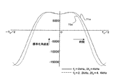
更に本実施例は、第1可動子11の周波数2f0が、温度等の外的な要因によって変化した場合でも、常に最小角速度V1、最大角速度V2を満たす偏向走査を達成するφ1、φ2を設定することができる。図5、図6は、横軸を時間tとして第1可動子11の周波数f0のねじり振動の変位角、角速度をそれぞれ説明する図である。図5は、特に第1可動子11のねじり振動の1周期T0に相当する部分(−T0/2<t<T0/2)を示しており、縦軸は、標準化変位角であって、式3における変位角θをφ1で除した値である。曲線71は、周波数2f0を4kHz(つまり基準周波数f0を2kHz)、最小角速度を8000rad/s、最大角速度を8800rad/sで、式7により、φ1を0.9902、φ2を−0.1768とした標準化変位角を示している。更に、図6は、曲線71を微分した曲線71aを示している。図6の縦軸は、第1可動子11の角速度をφ1で除した標準化角速度を示している。
Furthermore, in the present embodiment, even when the
図5、図6に破線で示した曲線72、72aは、最小・最大角速度を曲線71と等しく設定し、周波数2f0を4.4kHz(基準周波数f0を2.2kHz)としたものである。これは、温度等の外的な要因などによって周波数2f0が10%変化した場合の曲線71の変化を想定したものである。この場合においても、式7から好適な最大振幅を算出することが可能である。図示した曲線72、72aは、式7よりφ1を0.9002、φ2を−0.1607とした曲線である。このように、本実施例の光偏向器制御装置により、周波数2f0または、基準周波数f0が変化した場合でも、常に最小・最大角速度が同一の偏向走査を実現可能となる。特に本実施例に示したように2つの固有振動モードの周波数が互いに2倍となる関係を用いることによって、鋸波状の往復振動が達成できるため、本実施例は、光の偏向走査の片側(往路または復路)のみを用いる応用に好適な形態となる。更に本実施例では、単一の光偏向器で、正弦波の重ね合わせの往復振動を達成できるため、光走査系を小型化することができる。
(実施例2)
図8は本発明の光偏向器制御装置を含む光走査系の第2の実施例を示すブロック図である。本実施例では、第1の実施例と同一部分には、同一の符号を付し、説明を省略する。
(Example 2)
FIG. 8 is a block diagram showing a second embodiment of the optical scanning system including the optical deflector control device of the present invention. In the present embodiment, the same parts as those in the first embodiment are denoted by the same reference numerals, and description thereof is omitted.
図8の本実施例の光偏向器制御装置を含む光走査系は、第1の実施例と異なり、2つの光偏向器31、311を有している。それに伴って、変位角検知手段もそれぞれ32、322のように2つ有している。図7(a)には、光偏向器31、311の上面図を示した。図示のように、光偏向器31、311は、可動子23と、可動子23と機械的な支持体25を弾性支持するねじりバネ24で構成されている。これら全ての要素は、ねじり軸17を中心として駆動手段16によりねじり振動する。また、可動子23は、光を偏向するための図示しない反射面を有しており、可動子23のねじり振動によって、光源からの光を偏向走査する。特に、本実施例では、2つの光偏向器31、311は、構成要素は同一であるが、各要素の寸法が異なっている。そのため光偏向器31のねじり軸17を中心としたねじり振動について、周波数f0の1次の固有振動モードを有するのに対して、光偏向器311は、2倍の周波数2f0の1次の固有振動モードを有している。
Unlike the first embodiment, the optical scanning system including the optical deflector control device of the present embodiment in FIG. 8 has two
図7(b)は、光偏向器31、311の2つの光偏向器の配置を説明する概念図である。図7(b)に示すように光偏向器31は、可動子23a、支持体25a、ねじりバネ24aで構成されている。一方、光偏向器311は、可動子23b、支持体25b、ねじりバネ24bで構成されている。本実施例では、図示のように、光偏向器31、311はそれぞれのねじり軸17a、17bがほぼ平行に配置される。そして、光偏向器31、311は、それぞれの図示しない駆動手段16a、16bによって、それぞれの固有振動モードの周波数(つまり、ここでは、光偏向器31、311はそれぞれ周波数f0、2f0)で、ねじり軸17a、17bまわりにねじり振動で駆動される。2つの振動軸は必ずしも平行である必要はなく、所望される全体構成に応じて適当な角度で配置され得る。前述の式3の変位角で駆動される可動子による光の偏向と同等な偏向が光22に対して行われる限り、どの様な配置でもよい。配置の仕方によっては、光偏向器に入れた光が偏向されて、ほぼ元の方向に戻ってくるような形態にもでき、この場合、光の這い回しにおいて空間が有効に利用されてコンパクトな構成とできる。
FIG. 7B is a conceptual diagram for explaining the arrangement of the two
上記構成において、図示しない光源からの光22は、まず光偏向器31の可動子23aの反射面によって偏向走査される。その後、光偏向器311の可動子23bの反射面によって更に偏向走査される。上記のように、光偏向器31、311のねじり振動の周波数はf0、2f0と異なっているため、2つの反射面で反射され、偏向走査された光22は、第1の実施例で説明した式3と同一の2つの正弦振動の重ね合わせの振動で駆動される偏向器による偏向光としてあらわされる。本実施例では、重ね合わせの正弦振動の周波数の関係がf0、2f0と2倍で、位相差がないため、第1の実施例と同様の鋸波状の振動となる。したがって、本実施例の光偏向器31、311を用いた光走査系においても、第1の実施例の原理と全く同様に、鋸波状の振動によって、偏向走査の角速度は、変位角が正弦波であったときと比べ、実質的な等角速度となる領域を広く設定でき、偏向走査の全域に対する利用可能な領域を大きくできる。本実施例では、特に2つの固有振動モードの周波数が2倍の関係を説明したが、これを3倍にした場合は、重ね合わせの振動の形状は略三角波となる。この場合、偏向走査の往復で略等角速度の領域が現れるため、往復で等角速度を利用する応用に特に好適となる。
In the above configuration, light 22 from a light source (not shown) is first deflected and scanned by the reflecting surface of the
更に、本実施例では、第1の実施例と比べ、2つの光偏向器で構成することによって、それぞれの光偏向器は、可動子、ねじりバネが1つと比較的簡易な構造であるため、製造が容易で耐久性の高い光走査系とすることができる。 Further, in this embodiment, compared to the first embodiment, each optical deflector has a relatively simple structure with one mover and one torsion spring by being constituted by two optical deflectors. An optical scanning system that is easy to manufacture and highly durable can be obtained.
図8の構成の説明に戻ると、本実施例の光偏向器制御装置51は、第1の実施例と異なり、変位角検出手段32、322は、光偏向器31、311のそれぞれの可動子23a、23bの変位角を検知する。それぞれの変位角の検知信号は、第2バンドパス回路36、第1バンドパス回路35へそれぞれ送られる。第2バンドパス回路36は、可動子23aの振動のうち、周波数のf0の信号成分付近の周波数帯を通過させる。第2バンドパス回路36からの信号は、信号52a、52b、52c、52dのように第2ピーク検出回路43、駆動回路42、乗算器401、周波数検知回路34にそれぞれ送られる。52bからの信号は、第2制御目標値44となるように第2ゲイン制御回路46により最大振幅を調整されて、駆動回路42へ送られ、この駆動信号によって光偏向器31を駆動する。一方、52cからの信号は、乗算器401により周波数f0の倍の周波数2f0に変換され、第1制御目標値49となるように第1ゲイン制御回路50で最大振幅を調節された後、駆動回路421へ駆動信号を送る。駆動回路421は、この駆動信号によって光偏向器311を駆動する。
Returning to the description of the configuration in FIG. 8, the optical
本実施例においても、第1の実施例と同様に、演算回路37は式7によって最大角速度プリセット38、最小角速度プリセット39、周波数f0から第1制御目標値44、第2制御目標値49を決定することができる。
In this embodiment, as in the first embodiment, the maximum angular velocity preset 38
第1バンドパス回路35は、周波数2f0の信号成分付近の周波数帯を通過させる。第1バンドパス回路35からの信号は、第1ピーク検出回路47へ送られる。第1ピーク検出回路47、第2ピーク検出回路43はそれぞれの周波数信号の振幅を検知し、第1差分増幅器48、第2差分増幅器45へそれぞれ信号を送る。ここで第1差分増幅器48、第2差分増幅器45は、第1ゲイン制御回路50、第2ゲイン制御回路46をそれぞれ制御するため、信号線52bを経た周波数f0の信号と乗算器401を経た周波数2f0の信号が、第1制御目標値49、第2制御目標値44となるように、最大振幅を調整できる。
The first
以上のように光偏向器制御装置51は、第1の実施例と異なり1つの固有振動モードをもつ2つの光偏向器を組み合わせた光偏向器群において、第1の実施例と同様に、偏向走査の仕様である最小角速度V1、最大角速度V2を満たすφ1、φ2を、可動子23aの周波数f0によって決定することができる。特に本実施例に示したように2つの固有振動モードの周波数が互いに2倍となる関係を用いることによって、鋸波状の往復振動が達成できるため、光の偏向走査の片側(往路または復路)のみを用いる応用に好適な形態となる。本実施例においても、2つの可動子の周波数がほぼ同じ割合で、温度等の外的な要因によって変化した場合でも、常に最小角速度V1、最大角速度V2を満たす偏向走査を達成するφ1、φ2を設定することができる。
As described above, unlike the first embodiment, the optical
(第3の実施例)
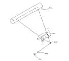
図9は上記光走査系を用いた光学機器の実施例を示す図である。ここでは光学機器として画像表示装置を示している。図9において、2006は、水平走査用光偏向器であり、投影面2005の水平方向に入射光を偏向走査する。一方、2001は本発明の光偏向器制御装置を含む光走査系であり、本実施例では、垂直方向に入射光を偏向走査する。2002はレーザ光源である。2003はレンズ或いはレンズ群であり、2004は書き込みレンズまたはレンズ群、2005は投影面である。レーザ光源2002から入射したレーザ光は、光の偏向走査のタイミングと関係した所定の強度変調を受けて光偏向器2006、光走査系2001により2次元的に走査される。この走査されたレーザ光は書き込みレンズ2004により投影面2005上に画像を形成する。
(Third embodiment)
FIG. 9 is a diagram showing an embodiment of an optical apparatus using the optical scanning system. Here, an image display device is shown as an optical apparatus. In FIG. 9,
本発明の光走査系を投影面2005の垂直方向の偏向走査に用いることによって、小型で省電力な共振を利用した光偏向器でありながら、略等角速度に光を偏向走査することができる。そのため、水平走査用光偏向器2006によって描画される画像の水平ラインのライン間隔を略一定とすることができ、画像の輝度むらをなくし、画像の垂直方向の全体サイズを一定にすることが可能となる。
By using the optical scanning system of the present invention for the deflection scanning in the vertical direction of the
更に、本発明の第1の実施例の光偏向器制御装置を用いることにより、光走査系2001の固有振動モードの周波数が温度などの外的要因で変化し、偏向走査の周波数が変化した場合でも、略等角速度となる領域の角速度を同一とすることが可能となる。したがって、画像の水平ラインのライン間隔を常に同一とし、画像の輝度むら、画像の垂直方向の全体サイズを常に一定にすることが可能となる。
Furthermore, when the optical deflector control device according to the first embodiment of the present invention is used, the frequency of the natural oscillation mode of the
(第4の実施例)
図10は上記光走査系を用いた光学機器の他の実施例を示す図である。ここでは、光学機器として画像形成装置を示している。図10において、3003は本発明の光偏向器制御装置を含む光走査系であり、本実施例では入射光を一次元に走査する。3001はレーザ光源である。3002はレンズあるいはレンズ群であり、3004は書き込みレンズ或いはレンズ群、3005は感光体である。レーザ光源3001から射出されたレーザ光は、光の偏向走査のタイミングと関係した所定の強度変調を受けて、光走査系3003により一次元的に走査される。この走査されたレーザ光は書き込みレンズ3004により、感光体3005上へ画像を形成する。感光体3005は図示しない帯電器により一様に帯電されており、この上に光を走査することによりその部分に静電潜像を形成する。次に、図示しない現像器により静電潜像の画像部分にトナー像を形成し、これを例えば図示しない用紙に転写・定着することで用紙上に画像が形成される。本発明の光偏向器制御装置により、光の偏向走査の角速度を仕様範囲内に設定することが可能となる。
(Fourth embodiment)
FIG. 10 is a diagram showing another embodiment of an optical apparatus using the optical scanning system. Here, an image forming apparatus is shown as an optical apparatus. In FIG. 10,
11、13 可動子
12、14、24、24a、24b ねじりバネ(弾性支持部)
15、25、25a、25b 支持体
16 固定コイル(駆動手段)
23、23a、23b 可動子(偏向反射面)
31、311、2001、3003 光偏向器(光走査系)
37 演算回路
42、421 駆動回路(駆動手段)
51 光偏向器制御装置
2002、3001 光源
2005 投影面(画像表示体)
3005 感光体
11, 13
15, 25, 25a,
23, 23a, 23b Movable element (deflection reflection surface)
31, 311, 2001, 3003 Optical deflector (optical scanning system)
37
51 Optical
3005 Photoconductor
Claims (8)
前記光偏向器によって偏向走査される光の偏向走査の角速度のプリセットされた最大値と最小値および前記周波数検知回路から出力される前記互いに異なる周波数の正弦振動のいずれか1つの周波数から、2つの前記偏向反射面の正弦振動の最大振幅の制御目標値を決定する演算回路を有することを特徴とする光偏向器制御装置。 Two deflection reflecting surfaces that perform sinusoidal vibrations of different frequencies in a proportional relationship in which one frequency is a constant multiple of the other frequency, two driving means for driving the two deflection reflecting surfaces, and a frequency detection circuit, An optical deflector control device for controlling an optical deflector that deflects and scans light from a light source by superimposing sinusoidal vibrations of the two deflection reflecting surfaces ;
From said one of the frequency of the sine vibrations of different frequencies from each other are output from the maximum value and the minimum value and the frequency detecting circuit which is preset angular speed of deflective scan of the deflecting scanned Ru light by the light deflector, the two An optical deflector control device comprising an arithmetic circuit for determining a control target value of a maximum amplitude of sinusoidal vibration of the deflecting reflecting surface.
周波数検知回路と、
振動系の有する一方の周波数が他方の周波数の定数倍である比例関係にある2つの異なる固有振動モードで振動系を駆動する駆動手段と、を有し、
光源からの光を偏向走査する光偏向器を制御する光偏向器制御装置であって、
前記光偏向器によって偏向走査される光の偏向走査の角速度のプリセットされた最大値と最小値および前記周波数検知回路から出力される前記2つの異なる固有振動モードのいずれか1つの周波数から、前記偏向反射面の2つの固有振動モードの最大振幅の制御目標値を決定する演算回路を有することを特徴とする光偏向器制御装置。 The deflection comprising two or more movers including a mover having a deflecting reflecting surface, a plurality of elastic support portions for connecting the movers, and a support body for supporting a part of the plurality of elastic support portions. A vibration system configured to allow the reflecting surface to vibrate around one vibration axis;
A frequency detection circuit;
Driving means for driving the vibration system in two different natural vibration modes in a proportional relationship in which one frequency of the vibration system is a constant multiple of the other frequency;
An optical deflector control device that controls an optical deflector that deflects and scans light from a light source,
From any one frequency of the two different natural vibration modes output from the maximum value and the minimum value and the frequency detecting circuit which is preset angular speed of deflective scan of the deflecting scanned Ru light by the light deflector, the deflector An optical deflector control device having an arithmetic circuit for determining a control target value of a maximum amplitude of two natural vibration modes of a reflecting surface.
前記光偏向器によって偏向走査される光の偏向走査の角速度の最大値と最小値をプリセットする第1の工程と、
前記互いに異なる周波数の正弦振動のいずれか1つの周波数を検知する第2の工程と、
前記第1の工程でプリセットした、偏向走査される光の偏向走査の角速度の最大値と最小値と、前記第2の工程で求めた周波数とから2つの前記偏向反射面の正弦振動の最大振幅の制御目標値を決定する工程と、を含むことを特徴とする光偏向器の制御方法。 Control of an optical deflector that deflects and scans light from a light source by superimposing sinusoidal vibrations of two deflection reflecting surfaces that perform sinusoidal vibrations of different frequencies that have a proportional relationship in which one frequency is a constant multiple of the other frequency. A method,
A first step of presetting the maximum and minimum values of the angular speed of deflective scan of the optical deflector by Ru is deflected scanning beam,
A second step of detecting any one of the sinusoidal vibrations having different frequencies;
Said preset in the first step, the maximum value and the minimum value of the deflection scan of the deflecting scanned Ru optical angular, the maximum amplitude of the sinusoidal oscillation of the two of the deflection reflecting surface and a frequency determined in the second step And determining a control target value for the optical deflector.
前記光偏向器によって偏向走査される光の偏向走査の角速度の最大値と最小値をプリセットする第1の工程と、A first step of presetting a maximum value and a minimum value of an angular velocity of deflection scanning of light deflected and scanned by the optical deflector;
前記振動系の有する一方の周波数が他方の周波数の定数倍である比例関係にある2つの異なる固有振動モードのいずれか1つの周波数を検知する第2の工程と、A second step of detecting any one frequency of two different natural vibration modes in a proportional relationship in which one frequency of the vibration system is a constant multiple of the other frequency;
前記第1の工程でプリセットした、偏向走査される光の偏向走査の角速度の最大値と最小値と、前記第2の工程で求めた周波数とから前記偏向反射面の2つの固有振動モードの最大振幅の制御目標値を決定する工程と、を含むことを特徴とする光偏向器の制御方法。The maximum of the two natural vibration modes of the deflecting / reflecting surface is preset from the maximum and minimum values of the angular velocity of the deflection scanning of the light to be deflected and preset in the first step, and the frequency obtained in the second step. Determining a control target value of the amplitude, and a method of controlling the optical deflector.
Priority Applications (1)
| Application Number | Priority Date | Filing Date | Title |
|---|---|---|---|
| JP2004162536A JP4447963B2 (en) | 2004-05-31 | 2004-05-31 | Optical deflector control device |
Applications Claiming Priority (1)
| Application Number | Priority Date | Filing Date | Title |
|---|---|---|---|
| JP2004162536A JP4447963B2 (en) | 2004-05-31 | 2004-05-31 | Optical deflector control device |
Publications (3)
| Publication Number | Publication Date |
|---|---|
| JP2005345574A JP2005345574A (en) | 2005-12-15 |
| JP2005345574A5 JP2005345574A5 (en) | 2007-07-19 |
| JP4447963B2 true JP4447963B2 (en) | 2010-04-07 |
Family
ID=35498046
Family Applications (1)
| Application Number | Title | Priority Date | Filing Date |
|---|---|---|---|
| JP2004162536A Expired - Fee Related JP4447963B2 (en) | 2004-05-31 | 2004-05-31 | Optical deflector control device |
Country Status (1)
| Country | Link |
|---|---|
| JP (1) | JP4447963B2 (en) |
Families Citing this family (8)
| Publication number | Priority date | Publication date | Assignee | Title |
|---|---|---|---|---|
| WO2005083493A1 (en) * | 2004-02-27 | 2005-09-09 | Matsushita Electric Industrial Co., Ltd. | Illuminating light source and two-dimensional image display using same |
| DE202005021930U1 (en) | 2005-08-01 | 2011-08-08 | Corning Cable Systems Llc | Fiber optic decoupling cables and pre-connected assemblies with toning parts |
| JP5441309B2 (en) * | 2006-02-13 | 2014-03-12 | キヤノン株式会社 | Oscillator device and optical deflection device |
| US7920313B2 (en) * | 2008-03-12 | 2011-04-05 | Canon Kabushiki Kaisha | Oscillator device, optical deflector and image forming apparatus using the optical deflector |
| JP5408887B2 (en) * | 2008-03-12 | 2014-02-05 | キヤノン株式会社 | Oscillator device and image forming apparatus using the oscillator device |
| JP5296428B2 (en) * | 2008-06-20 | 2013-09-25 | キヤノン電子株式会社 | Optical scanning apparatus, image forming apparatus using the optical scanning apparatus, image reading apparatus, and display |
| JP5424995B2 (en) * | 2010-06-24 | 2014-02-26 | キヤノン株式会社 | Optical scanning apparatus and image forming apparatus |
| JP5572584B2 (en) * | 2011-04-27 | 2014-08-13 | 京セラドキュメントソリューションズ株式会社 | Optical scanning device and image forming apparatus having the same |
-
2004
- 2004-05-31 JP JP2004162536A patent/JP4447963B2/en not_active Expired - Fee Related
Also Published As
| Publication number | Publication date |
|---|---|
| JP2005345574A (en) | 2005-12-15 |
Similar Documents
| Publication | Publication Date | Title |
|---|---|---|
| JP4574396B2 (en) | Optical deflector | |
| KR100806015B1 (en) | Micro-oscillating member, light-deflector, and image-forming apparatus | |
| JP5064864B2 (en) | Optical deflection apparatus, image forming apparatus, and driving method of optical deflection apparatus | |
| JP4881073B2 (en) | Optical deflector and optical instrument using the same | |
| JP5170983B2 (en) | Optical deflector and optical instrument using the same | |
| JP2007322466A (en) | Optical deflector and optical equipment using the same | |
| JP2005275198A (en) | Optical scanner and image forming apparatus comprising the same | |
| JP5164345B2 (en) | Optical scanning device and image forming apparatus using the same | |
| JP2007316443A (en) | Light deflector and optical equipment using the same | |
| US8254006B2 (en) | Oscillator device and optical deflector using the same | |
| JP7102705B2 (en) | Actuators, optics and projectors | |
| JP4447963B2 (en) | Optical deflector control device | |
| JP2009058616A (en) | Oscillating body apparatus, light deflector and image forming apparatus using the same | |
| US20100085618A1 (en) | Oscillator device, optical deflecting device and method of controlling the same | |
| JP2008058752A (en) | Light deflector and image forming apparatus using same | |
| JP2009025617A (en) | Oscillation body apparatus, optical deflector and optical apparatus using the same | |
| JP5554895B2 (en) | Oscillator structure and oscillator device using the oscillator structure | |
| JP2008299297A (en) | Rocking body apparatus and method of driving and controlling oscillation system of rocking body apparatus | |
| JP2008268879A (en) | Oscillator device, optical deflector and image forming apparatus using the optical deflector | |
| JP5341372B2 (en) | Oscillator device and image forming apparatus using the oscillator device | |
| JP2005250077A (en) | Optical deflector | |
| JP2005326745A (en) | Optical deflector and its control method | |
| JP5084385B2 (en) | Torsion spring, optical deflector, and image forming apparatus using the same | |
| JP2007163817A (en) | Optical deflector and optical equipment using the same | |
| JP2008170495A (en) | Oscillating body apparatus |
Legal Events
| Date | Code | Title | Description |
|---|---|---|---|
| A521 | Written amendment |
Free format text: JAPANESE INTERMEDIATE CODE: A523 Effective date: 20070531 |
|
| A621 | Written request for application examination |
Free format text: JAPANESE INTERMEDIATE CODE: A621 Effective date: 20070531 |
|
| A977 | Report on retrieval |
Free format text: JAPANESE INTERMEDIATE CODE: A971007 Effective date: 20080909 |
|
| A131 | Notification of reasons for refusal |
Free format text: JAPANESE INTERMEDIATE CODE: A131 Effective date: 20080916 |
|
| A521 | Written amendment |
Free format text: JAPANESE INTERMEDIATE CODE: A523 Effective date: 20081117 |
|
| A131 | Notification of reasons for refusal |
Free format text: JAPANESE INTERMEDIATE CODE: A131 Effective date: 20091001 |
|
| A521 | Written amendment |
Free format text: JAPANESE INTERMEDIATE CODE: A523 Effective date: 20091119 |
|
| TRDD | Decision of grant or rejection written | ||
| A01 | Written decision to grant a patent or to grant a registration (utility model) |
Free format text: JAPANESE INTERMEDIATE CODE: A01 Effective date: 20100119 |
|
| A01 | Written decision to grant a patent or to grant a registration (utility model) |
Free format text: JAPANESE INTERMEDIATE CODE: A01 |
|
| A61 | First payment of annual fees (during grant procedure) |
Free format text: JAPANESE INTERMEDIATE CODE: A61 Effective date: 20100121 |
|
| FPAY | Renewal fee payment (event date is renewal date of database) |
Free format text: PAYMENT UNTIL: 20130129 Year of fee payment: 3 |
|
| R150 | Certificate of patent or registration of utility model |
Free format text: JAPANESE INTERMEDIATE CODE: R150 |
|
| FPAY | Renewal fee payment (event date is renewal date of database) |
Free format text: PAYMENT UNTIL: 20140129 Year of fee payment: 4 |
|
| LAPS | Cancellation because of no payment of annual fees |