JP4438039B2 - Color filter manufacturing method and manufacturing apparatus, liquid crystal panel manufacturing method, display device manufacturing method, display device panel manufacturing method - Google Patents
Color filter manufacturing method and manufacturing apparatus, liquid crystal panel manufacturing method, display device manufacturing method, display device panel manufacturing method Download PDFInfo
- Publication number
- JP4438039B2 JP4438039B2 JP2000225896A JP2000225896A JP4438039B2 JP 4438039 B2 JP4438039 B2 JP 4438039B2 JP 2000225896 A JP2000225896 A JP 2000225896A JP 2000225896 A JP2000225896 A JP 2000225896A JP 4438039 B2 JP4438039 B2 JP 4438039B2
- Authority
- JP
- Japan
- Prior art keywords
- ink
- wiping
- color filter
- manufacturing
- discharge port
- Prior art date
- Legal status (The legal status is an assumption and is not a legal conclusion. Google has not performed a legal analysis and makes no representation as to the accuracy of the status listed.)
- Expired - Fee Related
Links
Images


Description
【0001】
【発明の属する技術分野】
本発明は、ヘッドにより基板上の画素を着色することにより表示装置用のパネル(表示用素子)を製造するための、表示装置用のパネルの製造方法及び製造装置に関し、例えばカラーテレビ、パーソナルコンピュータ等に使用されるカラーフィルタの製造方法及び製造装置、表示装置の製造方法、表示装置を備えた装置の製造方法等に関するものである。
【0002】
【従来の技術】
近年携帯用パーソナルコンピュータの急速な発達に伴い、液晶デイスプレイ、特にカラー液晶デイスプレイの需要は増加する傾向にある。同時に、装置のコストダウンも要求されるようになり、特に比較的コスト比率の高いカラーフィルタのコストダウンに対する要求が高まっている。カラーフィルタの要求特性を満足し、上記の要求も満たすため様々な方法が試されているが、いまだ不十分である。以下にそれぞれの方法について説明する。
【0003】
最も多く使われている第1の方法が顔料分散法である。この方法は、まず基板上に顔料を分散した感光性樹脂層を形成し、これをパターンニングすることにより単色のパターンを得る。さらにこの工程を3回繰り返すことによりR,G,Bのカラーフィルター層を得る。
【0004】
第2の方法は、染色法である。この方法はガラス基板上に染色用の材料である水溶性の高分子材料を形成し、フォトリソグラフィー工程によりある形状にパターンニングして、できあがったパターンを染色浴に浸漬して着色されたパターンを得る。これを3回繰り返すことにより、R,G,Bのカラーフィルタを形成する。
【0005】
第3の方法として電着法がある。この方法は、まず基板上に透明基板をパターニングする。つぎに顔料、樹脂、電解液等の入った電着塗装液に浸漬し第1の色を電着する。この工程を3回繰り返してR,G,Bの着色層を形成し、最後に焼成する。
【0006】
第4の方法として、印刷法がある。この方法は、熱硬化性樹脂に顔料を分散させ、印刷を3回繰り返すことによりR,G,Bを塗り分けた後、樹脂を熱硬化させることにより着色層を形成するものである。また、いずれの方法においても着色層上に保護層を形成するのが一般的である。
【0007】
従来の方法に共通している点は、R,G,Bの3色を着色するために同一の工程を3回繰り返す必要があり、コスト高になることである。また、工程が多いほど歩留まりが低下するという問題を有している。さらに、電着法においては、形成可能なパターン形状が限定されるため、現状の技術では、TFT用には適用困難である。また、印刷法は、解像度が悪いためファインピッチのパターンの形成には不向きである。
【0008】
【発明が解決しようとする課題】
これらの欠点を補うべく、インクジェットを用いたカラーフィルターの製造方法として、特開昭59−75205号、特開昭63−235901号、特開平1−217320号、特開平4−123005号、特開平9−138306号等の提案がある。これらは、前記従来の方法とは異なりR(赤),G(緑),B(青)の各色のインクを光透過性の基板上の所定の位置にインクジェットヘッドより噴射し、インクを基板上で乾燥させて着色層を形成させるものである、この方法によればR,G,Bの各色層の形成を一度に行うことができ、さらにインクの使用量にも無駄が生じないため大幅な生産性の向上、コストダウン等の効果を得ることができる。
【0009】
このようなインクジェット方式を用いてカラーフィルタを製造する場合、インクジェットヘッドはインクの吐出を繰り返すうちにそのノズル面(吐出口面)がインクで汚れてくるため、定期的にノズル面の清掃を行う必要がある。
【0010】
従来、このノズル面の清掃は、弾性を有するスポンジ状のワイピング部材でインクジェットヘッドのノズル面をワイピングすることにより行われていた。
【0011】
この際に、インクジェットヘッドのノズルが並ぶ方向、あるいはノズル列に対して直角な方向にワイピング部材を動かすことにより清掃をすることが一般的であった。
【0012】
通常は、インクジェットヘッドのノズル面のワイピングを繰り返すことにより、徐々にノズル面のノズル穴付近に細かな傷が生じたり、撥水部分の撥水効果が低下することによりインクジェットへッドから吐出されるインク滴の飛翔方向が微妙に変化し、着弾位置のずれが発生する。
【0013】
このような着弾位置のずれは、一般のインクジェットプリンタでは問題にならないレベルであるが、カラーフィルター等の高精細なパターンの着色においては、隣接する着色領域との混色を引き起こすため歩留まりを下げる大きな問題となっていた。
【0014】
従って、本発明は上述した課題に鑑みてなされたものであり、その目的は、インクジェットヘッドのノズル面(吐出口面)のワイピングを繰り返しても、歩留まりを低下させること無くカラーフィルターを製造することができるカラーフィルターの製造方法および製造装置、その製造方法により製造されたカラーフィルタ、該カラーフィルタを備えた表示装置の製造方法、該表示装置を備えた装置の製造方法、表示装置用パネルの製造方法および製造装置を提供することである。
【0015】
【課題を解決するための手段】
上述した課題を解決し、目的を達成するために、本発明に係わるカラーフィルタの製造方法は、インクを吐出するための吐出口が形成された吐出口面を有し、少なくとも前記吐出口の周辺部分が撥水部材で被覆されたインクジェットヘッドから基板上にインクを吐出して、所定の方向に延びる着色領域を色毎に形成することによりカラーフィルタを製造する方法であって、前記吐出口面をワイピングするためのワイピング部材により前記吐出口面をワイピングする工程を備え、前記ワイピング部材によるワイピング方向は前記所定の方向に沿った方向と同一であることを特徴としている。
【0016】
また、本発明に係わるカラーフィルタの製造方法は、インクを吐出するための吐出口が形成された吐出口面を有し、当該吐出口の周辺部分が撥水部材で被覆されたインクジェットヘッドと基板とを所定方向に相対移動させながら、同じ色のインクで形成される複数の画素を前記所定方向に配列してなるカラーフィルタを製造する方法であって、前記同じ色のインクで形成される2つの画素の間隔と、前記インクジェットヘッドの複数の吐出口のうち使用する2つの吐出口の、前記所定の方向と直交する方向における間隔とが一致するように、前記インクジェットヘッドの前記所定の方向に対する角度を調整する調整工程と、前記調整工程において調整された角度を保ったままの状態で前記インクジェットヘッドから前記相対移動中に前記基板にインクを吐出する工程と、前記調整工程において調整された角度を保ったままの状態で前記吐出口面をワイピング部材によりワイピングする工程とを具備し、前記ワイピング部材のワイピングの方向は前記所定の方向に沿った方向と同一であることを特徴としている。
【0017】
また、本発明に係わる液晶パネルの製造方法は、カラーフィルタを備えた液晶パネルの製造方法であって、上記の製造方法により製造されたカラーフィルタを用意する工程と、用意された前記カラーフィルタと対向基板との間に液晶化合物を挿入する工程と、を具備することを特徴としている。
【0018】
また、本発明に係わる表示装置の製造方法は、液晶パネルを備えた表示装置の製造方法であって、上記の製造方法により製造された液晶パネルを用意する工程と、用意された前記液晶パネルに画像信号を供給する画像信号供給手段を接続する工程と、を具備することを特徴としている。
【0019】
また、本発明に係わる表示装置用パネルの製造方法は、液体を吐出するための吐出口が形成された吐出口面を有し、当該吐出口の周辺部分が撥水部材で被覆された液体付与ヘッドから基板上に液体を付与することで、所定の方向に延び且つ表示に用いられる表示部が配列してなる表示装置用パネルを製造する方法であって、前記吐出口面をワイピングするためのワイピング部材により前記吐出口面をワイピングする工程を備え、前記ワイピング部材によるワイピング方向は前記所定の方向に沿った方向と同一であることを特徴としている。
【0020】
また、本発明に係わる表示装置用パネルの製造方法は、表示に用いられるための材料を吐出するための吐出口が形成された吐出口面を有し、少なくとも前記吐出口の周辺部分が撥水部材で被覆されたヘッドから基体上に前記材料を吐出して、所定の方向に延び且つ表示に用いられる表示部を形成することにより表示装置用パネルを製造する方法であって、同じ材料で形成される2つの前記表示部の間隔と、前記ヘッドの複数の吐出口のうち使用する2つの吐出口の、前記所定の方向と直交する方向における間隔とが一致するように、前記ヘッドの前記所定の方向に対する角度を調整する調整工程と、前記調整工程において調整された角度のままの状態で前記吐出口面をワイピング部材によりワイピングする工程とを具備し、 前記ワイピング部材によるワイピング方向は前記所定の方向に沿った方向と同一であることを特徴としている。
【0021】
また、本発明に係わるカラーフィルタの製造装置は、インクを吐出するための吐出口が形成された吐出口面を有し、少なくとも前記吐出口の周辺部分が撥水部材で被覆されたインクジェットヘッドから基板上にインクを吐出して、所定の方向に延びる着色領域を色毎に形成することによりカラーフィルタを製造する装置であって、前記吐出口面をワイピングするためのワイピング部材を備え、前記ワイピング部材によるワイピング方向は前記所定の方向に沿った方向と同一であることを特徴としている。
【0029】
【発明の実施の形態】
以下、本発明の好適な一実施形態について、添付図面を参照して詳細に説明する。
【0030】
なお、本発明において定義する表示装置用パネル(表示用素子)とは、表示に用いられる表示部を有するものである。より具体的には、表示装置用パネルとは、例えば着色部を備えるカラーフィルタあるいは自己発光する材料により形成された発光部を備えるEL素子等を含む、表示装置に使用されるパネルのことである。尚、カラーフィルタであれば着色部が上記表示部に相当し、EL素子であれば発光部が上記表示部に相当する。また、本発明において定義するカラーフィルタとは、着色部と基体とを備えるものであり、入力光に対し、特性を変えた出力光を得ることができるものである。なお、基体とは、ガラスやプラスチック等の基板を含むものであり、また板状以外の形状も含むものである。なお、カラーフィルタにおいて所定の方向に延びる着色領域という表現は、図38の(a)に示すように、画素が一列に長い場合、あるいは(b)、(c)、(d)に示すように一列内が複数の画素に区切られている場合等を含むものである。また、カラーフィルタの着色領域は、視覚的に色を認識するための領域ということもできる。さらに、本実施形態で着色に使用されるインクジェットヘッドは、インク吐出口が開口した吐出口面を有し、少なくともこの吐出口の開口の周辺部分が所定の材料で被覆されているものである。また、インクジェットヘッドは、カラーフィルタ基板に着色された液体であるインクを付与するものであるので、液体付与ヘッドと呼ぶこともできる。
【0031】
図1はインクジェット法によるカラーフィルタの製造装置の構成を示す概略図であり、着色工程の作業中の状態を示している。
【0032】
図1において、51は装置架台、52は架台51上に配置されたXYZθステージ、53はXYZθステージ52上にセットされたカラーフィルタ基板、54はカラーフィルタ基板53上に形成されるカラーフィルタ、55はカラーフィルタ54の着色を行う赤色、緑色、青色の各インクジェットヘッドとそれらを支持するヘッドマウント55aとからなるヘッドユニット、58はカラーフィルタ製造装置90の全体動作を制御するコントローラ、59はコントローラの表示部、60はコントローラの操作部であるキーボードを示している。
【0033】
ヘッドユニット55はカラーフィルター製造装置の支持部90aに対して着脱自在に、かつ水平面内で回動角度を調整可能に装着されている。
【0034】
図2はカラーフィルタ製造装置90の制御コントローラの構成図である。59は制御コントローラ58の入出力手段であるティーチングペンダント、62は製造の進行状況及びヘッドの異常の有無等の情報を表示する表示部、60はカラーフィルタ製造装置90の動作等を指示する操作部(キーボード)である。
【0035】
58はカラーフィルタ製造装置90の全体動作を制御するところのコントローラ、65はティーチングペンダント59とのデータの受け渡しを行うインタフェース、66はカラーフィルタ製造装置90の制御を行うCPU、67はCPU66を動作させるための制御プログラムを記憶しているROM、68は異常情報等を記憶するRAM、70はカラーフィルタの各画素内へのインクの吐出を制御する吐出制御部、71はカラーフィルタ製造装置90のXYZθステージ52の動作を制御するステージ制御部、90はコントローラ58に接続され、その指示に従って動作するカラーフィルタ製造装置を示している。
【0036】
次に、図3は、上記のカラーフィルタ製造装置90に使用されるインクジェットヘッドIJHの構造を示す図である。図1の装置においては、インクジェットヘッドはR,G,Bの3色に対応して3個設けられているが、これらの3個のヘッドは夫々同一の構造であるので、図3にはこれらの3個のヘッドのうちの1つの構造を代表して示している。
【0037】
図3において、インクジェットヘッドIJHは、インクを加熱するための複数のヒータ102が形成された基板であるヒータボード104と、このヒータボード104の上にかぶせられる天板106とから概略構成されている。天板106には、複数の吐出口108が形成されており、吐出口108の後方には、この吐出口108に連通するトンネル状の液路110が形成されている。各液路110は、隔壁112により隣の液路と隔絶されている。各液路110は、その後方において1つのインク液室114に共通に接続されており、インク液室114には、インク供給口116を介してインクが供給され、このインクはインク液室114から夫々の液路110に供給される。
【0038】
ヒータボード104と、天板106とは、各液路110に対応した位置に各ヒータ102が来る様に位置合わせされて図3の様な状態に組み立てられる。図3においては、2つのヒータ102しか示されていないが、ヒータ102は、夫々の液路110に対応して1つずつ配置されている。そして、図3の様に組み立てられた状態で、ヒータ102に所定の駆動パルスを供給すると、ヒータ102上のインクが沸騰して気泡を形成し、この気泡の体積膨張によりインクが吐出口108から押し出されて吐出される。従って、ヒータ102に加える駆動パルスを制御、例えば電力の大きさを制御することにより気泡の大きさを調整することが可能であり、吐出口から吐出されるインクの体積を自在にコントロールすることができる。尚、カラーフィルタを製造する場合、各吐出口から吐出される各々のインク体積(インク吐出量)を略同一に揃えることが好ましい。各吐出インクの量が同一である場合、同一でない場合に比べ画素間のムラをより低減できるからである。
【0039】
図4は、インクジェットヘッドによりカラーフィルタを製造する例を示した図である。
【0040】
本発明のカラーフィルタにおいては、基板1として透光性の基板が好ましく、一般にガラス基板が用いられるが、液晶用カラーフィルタとしての透明性、機械的強度等の必要特性を有するものであればガラス基板に限定されるものではない。
【0041】
基板1上には、カラーフィルタを構成する各画素3を仕切るための仕切り部材(例えばブラックマトリクス)2が形成されている。このブラックマトリクス2により仕切られた開口部である画素3aに、インクジェットヘッド55b,55c,55dにより、赤(R)、緑(G)、あるいは青(B)のいずれかに着色された色インクを吐出し、画素3aを着色する。なお、インクジェットヘッド55b,55c,55dは、基板1に対して、図中矢印Aで示される方向に走査されながら基板1に向けてインクを吐出し、各画素3aを着色する。
【0042】
また、本発明で使用するインクジェット方式としては、エネルギー発生素子として電気熱変換体を用いたバブルジェット(登録商標)タイプ、あるいは圧電素子を用いたピエゾジェットタイプ等が使用可能であり、着色面積及び着色パターンは任意に設定することができる。
【0043】
図5はカラーフィルタの製造工程を示す図である。
【0044】
カラーフィルタ形成面として光透過性の基板1上に遮光部としてのブラックマトリクス2を形成する(工程(a))。
【0045】
基板1としては、一般にガラスが用いられるが、カラーフィルタとしての透明性を損なわず、機械的強度等カラーフィルタの用途に応じた必要特性を有するものであればプラスチックなどの樹脂でも使用可能である。
【0046】
またブラックマトリクス2は、基板上にスパッタもしくは真空蒸着などの成膜法によりクロム等の金属膜を形成し、フォトリソ法により開口部などをパターニングして形成する。ブラックマトリクス2としてはこの他に感光性の黒色樹脂を塗布後フォトリソ法によりパターニングして形成したものや、印刷法により形成したものなどが使用可能である。
【0047】
次に、基板上にインク受容層3を形成する(工程(b))。
【0048】
インク受容層3はそれ自身ではインク受容性を持たないが、ある条件下においてインク受容性を示すポジ型、あるいはそれ自身はインク受容性を持つが、ある条件下でインク受容性を失うネガ型、いずれかの性質を有し、且つある条件下で硬化する特性を有する樹脂組成物をカラーフィルタ形成面に塗布し、必要に応じてプリベークを行って形成する。上記のある条件下とは、たとえば光照射、又は光照射及び熱照射などである。上記樹脂組成物の塗布には、スピンコート、ロールコート、バーコート、スプレーコート、ディップコート等の塗布方法を用いることができる。本発明においては光照射により硬化しその部分がインクを吸収しなくなるネガ型の感光性樹脂組成物を用いるのが望ましい。
【0049】
またインク受容層3の厚さは、本実施形態のカラーフィルタを液晶素子に用いる場合で0.3〜3.0μm程度である。
【0050】
フォトマスク4を用いてインク受容層3をパターン露光し、その一部を硬化してインク受容性を失った撥インク部5を形成する(工程(c))。
【0051】
この場合の図に示したフォトマスク4は、インク受容層3をネガ型の感光性樹脂組成物を用いて形成する場合である。インク受容層3としてポジ型の感光性樹脂組成物を用いて形成する場合は図に示したフォトマスク4とは逆のフォトマスクを用い撥インク部をマスクしてパターン露光すれば良い。
【0052】
図に示したように撥インク部5は、ブラックマトリクス2に重なる位置に形成される。該撥インク部5の幅はブラックマトリクスの幅より狭くなるように形成することが好ましく、液晶素子に用いる場合で1.0〜30.0μm程度である。これにより後述の着色部9a〜9cがブラックマトリクス2と重なる位置にまで延出して形成され、白抜けが防止できる。
【0053】
インクジェットヘッド55からR,G,Bの各色のインク10をインク受容層3の未露光部6の所定の位置に付与する(工程(d)、工程(e))。
【0054】
各未露光部は撥インク層5により周囲を囲まれている。
【0055】
本発明においてインクジェット方式としてはエネルギー発生素子として電気熱変換体を用いたバブルジェットタイプ、あるいは圧電素子を用いたピエゾジェットタイプ等が使用可能であり、着色面積及び着色パターンは任意に設定することができる。
【0056】
また本発明において、着色用のインクとしては染料系、顔料系共に用いることが可能である。また、常温で液体のものに限らず、室温やそれ以下で固化するインクであって、室温で軟化するもの、もしくは液体であるもの、あるいは上述のインクジェット方式ではインク自体を30℃以上70℃以下の範囲内で温度調整をおこなってインクの粘性を安定吐出範囲にあるように温度制御するものが一般的であるから、使用記録信号付与時にインクが液状をなすものが好適に用いられる。
【0057】
さらに必要に応じてインクの乾燥を行い、熱処理を行いインク受容層3全体を完全に硬化させインクを定着させ、各色の着色部9a〜9cを形成する。これによりカラーフィルター54が形成される。この後必要に応じて、カラーフィルター54上に保護層8を形成するのが一般的である(工程(f))。
【0058】
保護層8としては、光硬化型、熱硬化型、あるいは光、熱併用型の樹脂膜、蒸着やスパッタ等により形成される無機膜などを用いることができ、カラーフィルタとしての透明性を有し、その後のITO形成工程、配向膜形成工程等に耐えられるものであれば使用することができる。
【0059】
(第2の方法)
図25は第2の方法の工程図であり、図5と同じ部材には同じ符号を付した。また、図25の(a)〜(d)は下記工程(a)〜(d)に対応する模式図である。
【0060】
工程(a)
まず、透明基板1上に隔壁部(仕切り部材)を形成する。隔壁部は後述するインクを付与した際に隣接する異なる色のインクとの混色を避けるための部材であり、本例では遮光層を兼ねたブラックマトリクス342とした。当該ブラックマトリクス342としては、好ましくは黒色顔料含有レジストを用い、一般的なフォトリソグラフィ法によりパターニングする。該ブラックマトリクス342は後述するインクを付与した際に、隣接する異なるインク同士が混じり合うのを防止するために、好ましくは撥インク性を付与しておく。本発明においてブラックマトリクス342の厚さは上記隔壁作用及び遮光作用を考慮すると0.5μm以上が好ましい。また、該ブラックマトリクス342の開口部が本発明にかかる被着色部である。
【0061】
工程(b)
インクジェットヘッド37より、R、G、Bの各色のインク343をブラックマトリクス342の開口部を埋めるように所定の着色パターンにしたがって付与する。本発明においては、当該工程において、前記実施形態で説明したように、各非着色部に複数のノズルからインクを付与する。
【0062】
本発明で用いられるインクは、エネルギー付与により硬化し、通常着色剤を含有する樹脂組成物からなる。上記着色剤としては一般の染料や顔料を用いることができ、例えば染料としては、アントラキノン染料、アゾ染料、トリフェニルメタン染料、ポリメチン染料などを用いることができる。
【0063】
またインクに用いる樹脂としては、熱処理や光照射等のエネルギー付与によって硬化する樹脂を用いる。具体的には、熱硬化型樹脂として、公知の樹脂と架橋剤との組み合わせが使用できる。例えば、アクリル樹脂、メラミン樹脂、水酸基あるいはカルボキシル基含有ポリマーとメラミン、水酸基あるいはカルボキシル基含有ポリマーと多官能エポキシ化合物、水酸基あるいはカルボキシル基含有ポリマーと繊維素反応型化合物、エポキシ樹脂とレゾール型樹脂、エポキシ樹脂とアミン類、エポキシ樹脂とカルボン酸又は酸無水物、エポキシ化合物などが挙げられる。また、光硬化型樹脂としては、公知のもの、例えば市販のネガ型レジストが好適に用いられる。
【0064】
上記インクには、種々の溶媒を加えることもできる。特に、インクジェット方式での吐出性の面から、水及び水溶性有機溶剤の混合溶媒が好ましく用いられる。
【0065】
さらに、上記成分の他に必要に応じて所望の特性を持たせるために、界面活性剤、消泡剤、防腐剤等を添加することができ、さらに、市販の水溶性染料なども添加することができる。
【0066】
また、上記した光或いは熱硬化型樹脂のうち、水あるいは水溶性有機溶剤に溶解しないものでも安定に吐出可能なものであれば、水や水溶性有機溶剤以外の溶媒を用いてもかまわない。また、特に光により重合するタイプのモノマーを用いる場合には、染料をモノマーに溶解した無溶剤タイプとすることもできる。
【0067】
工程(c)
樹脂ブラックマトリクス342の開口部に付与したインク343を熱処理あるいは光照射、あるいはその両者によって硬化させ、着色部344を形成する。
【0068】
工程(d)
必要に応じて保護層8を形成する。
【0069】
図6乃至図8は、本発明により製造されたカラーフィルタを組み込んだカラー液晶表示装置30の基本構成を示す断面図である。
【0070】
本発明におけるカラー液晶表示装置(カラー液晶ディスプレイ)は、本発明に係るカラーフィルタの製造方法を用いて製造されたカラーフィルタ基板1と対向基板21を合わせこみ、液晶化合物18を封入することにより形成される。液晶表示装置の一方の基板21の内側に、TFT(Thin Film Transistor)(不図示)と透明な画素電極20がマトリクス状に形成される。また、もう一方の基板1の内側には、画素電極に対向する位置にRGBの色材が配列するようカラーフィルタ54が設置され、その上に透明な対向電極(共通電極)16が一面に形成される。ブラックマトリクス2は、通常カラーフィルター基板1側に形成されるが(図6参照)、BM(ブラックマトリクス)オンアレイタイプの液晶パネルにおいては対向するTFT基板側に形成される(図7参照)。さらに、両基板の面内には配向膜19が形成されており、これをラビング処理することにより液晶分子を一定方向に配列させることができる。また、それぞれのガラス基板の外側には偏光板11,22が接着されており、液晶化合物18は、これらのガラス基板の間隙(2〜5μm程度)に充填される。また、バックライトとしては蛍光灯(不図示)と散乱板(不図示)の組み合わせが一般的に用いられており、液晶化合物をバックライト光の透過率を変化させる光シャッターとして機能させることにより表示を行う。尚、液晶化合物は、カラーフィルタに照射される光量を可変する機能を有しているため、光量可変手段ともいえる。
【0071】
また、図8に示すように、画素電極20上に着色部を形成し、カラーフィルタとして機能させるようにしても良い。すなわち、カラーフィルタを構成する着色部は、ガラス基板上に形成されることに限定されるものではない。
【0072】
このような液晶表示装置を情報処理装置に適用した場合の例を図9乃至図11を参照して説明する。尚、この情報処理装置は、本発明に係る製造方法を用いて製造されたカラーフィルタを有する液晶表示装置に画像信号を供給する画像信号供給手段を接続することにより製造されるものである。
【0073】
図9は上記の液晶表示装置をワードプロセッサ、パーソナルコンピュータ、ファクシミリ装置、複写装置としての機能を有する情報処理装置に適用した場合の概略構成を示すブロック図である。
【0074】
図中、1801は装置全体の制御を行う制御部(画像信号供給手段)で、マイクロプロセッサ等のCPUや各種I/Oポートを備え、各部に制御信号やデータ信号等を出力したり、各部よりの制御信号やデータ信号を入力して制御を行っている。1802はディスプレイ部で、この表示画面には各種メニューや文書情報及びイメージリーダ1807で読み取ったイメージデータ等が表示される。1803はディスプレイ部1802上に設けられた透明な感圧式のタッチパネルで、指等によりその表面を押圧することにより、ディスプレイ部1802上での項目入力や座標位置入力等を行うことができる。
【0075】
1804はFM(Frequency Modulation)音源部で、音楽エディタ等で作成された音楽情報をメモリ部1810や外部記憶装置1812にデジタルデータとして記憶しておき、それらメモリ等から読み出してFM変調を行うものである。FM音源部1804からの電気信号はスピーカ部1805により可聴音に変換される。プリンタ部1806はワードプロセッサ、パーソナルコンピュータ、ファクシミリ装置、複写装置の出力端末として用いられる。
【0076】
1807は原稿データを光電的に読取って入力するイメージリーダ部で、原稿の搬送経路中に設けられており、ファクシミリ原稿や複写原稿の他各種原稿の読取りを行う。
【0077】
1808はイメージリーダ部1807で読取った原稿データのファクシミリ送信や、送られてきたファクシミリ信号を受信して復号するファクシミリ(FAX)の送受信部であり、外部とのインタフェース機能を有する。1809は通常の電話機能や留守番電話機能等の各種電話機能を有する電話部である。
【0078】
1810はシステムプログラムやマネージャープログラム及びその他のアプリケーションプログラム等や文字フォント及び辞書等を記憶するROMや、外部記憶装置1812からロードされたアプリケーションプログラムや文書情報、さらにはビデオRAM等を含むメモリ部である。
【0079】
1811は文書情報や各種コマンド等を入力するキーボード部である。
【0080】
1812はフロッピーディスクやハードディスク等を記憶媒体とする外部記憶装置で、この外部記憶装置1812には文書情報や音楽あるいは音声情報、ユーザのアプリケーションプログラム等が格納される。
【0081】
図10は図9に示す情報処理装置の模式的概観図である。
【0082】
図中、1901は上記の液晶表示装置を利用したフラットパネルディスプレイで、各種メニューや図形情報及び文書情報等を表示する。このディスプレイ1901上ではタッチパネル1803の表面は指等で押圧することにより座標入力や項目指定入力を行うことができる。1902は装置が電話機として機能するときに使用されているハンドセットである。キーボード1903は本体と着脱可能にコードを介して接続されており、各種文書機能や各種データ入力を行うことができる。また、このキーボード1903には各種機能キー1904等が設けられている。1905は外部記憶装置1812へのフロッピーディスクの挿入口である。
【0083】
1906はイメージリーダ部1807で読取られる原稿を載置する用紙載置部で、読取られた原稿は装置後部より排出される。またファクシミリ受信等においては、インクジェットプリンタ1907よりプリントされる。
【0084】
上記情報処理装置をパーソナルコンピュータやワードプロセッサとして機能する場合、キーボード部1811から入力された各種情報が制御部1801により所定のプログラムに従って処理され、プリンタ部1806に画像として出力される。
【0085】
ファクシミリ装置の受信機として機能する場合、通信回線を介してFAX送受信部1808から入力したファクシミリ情報が制御部1801により所定のプログラムに従って受信処理され、プリンタ部1806に受信画像として出力される。
【0086】
また、複写装置として機能する場合、イメージリーダ部1807によって原稿を読取り、読取られた原稿データが制御部1801を介してプリンタ部1806に複写画像として出力される。なお、ファクシミリ装置の受信機として機能する場合、イメージリーダ部1807によって読取られた原稿データは、制御部1801により所定のプログラムに従って送信処理された後、FAX送受信部1808を介して通信回線に送信される。
【0087】
なお、上述した情報処理装置は図11に示すようにインクジェットプリンタを本体に内蔵した一体型としてもよく、この場合は、よりポータブル性を高めることが可能となる。同図において、図10と同一機能を有する部分には、対応する符号を付す。このように表示装置を備えた装置は、▲1▼まず、本発明に係る製造方法によりカラーフィルタを製造し、▲2▼次に、そのカラーフィルタと対向基板との間に液晶化合物を充填して表示装置を製造し、▲3▼最後に、その表示装置に、画像信号供給手段を接続することにより、製造されるものである。
【0088】
次に、図12は複数のノズルを備えたインクジェットヘッドのノズル面を示す図である。
【0089】
本実施形態において、図12に示すようにノズル列方向と、ノズル列直角方向を定義することにする。
【0090】
図13は回復ユニット230を示す構成図である。
【0091】
図13において、231a,231b,231cはインクジェットヘッドの、赤色ヘッド55b、緑色ヘッド55c、青色ヘッド55cにそれぞれ対応したキャップである。キャップ231a,231b,231cは、インクジェットヘッド55b,55c,55dが、ガラス基板1にカラーフィルタの着色動作を行わない時に、それぞれ対応するインクジェットヘッド55b,55c,55dのノズル面をカバーすることによって、インクが吐出不能になることを防止する。
【0092】
232a,232b,232cはノズル面のワイピング動作を行うブレード(ワイピング部材)であり、例えばスポンジなどのように吸水性のあるものが好ましい。
【0093】
ブレード232a,232b,232cは、図13に示すように、回復系ユニット230のXY方向の動作により、それぞれインクジェットヘッド55b,55c,55dのノズル面についたインク滴や、インクを吐出した際に発生するインクミストがノズル面に付着したものを拭き取るためのものである。
【0094】
本実施形態においては、回復系ユニット230の動作方向であるXY方向は、X方向が図12で示したノズル列方向、Y方向が図12で示したノズル列直角方向と同一方向であるものとする。
【0095】
図14及び図15は、図13に示した回復ユニット230をY方向(ノズル列直角方向)に動作させ、ワイピング動作を繰り返した場合の着弾位置のずれを測定した結果を示すグラフである。
【0096】
図14はノズル列直角方向(ワイピング動作方向)の着弾位置のずれを測定した結果を示すグラフであり、図15はノズル列方向の着弾位置のずれを測定した結果を示すグラフである。
【0097】
図14、図15からわかるように、ワイピング動作方向であるノズル列直角方向に関してはワイピング回数増加に伴い、着弾位置のずれが徐々に大きくなっている。一方で、ノズル列方向に開しては、ワイピング回数が増加しても着弾位置のずれはほとんど変化が無い。
【0098】
このことから、ワイピングの方向と着弾位置のずれの方向が関係していることは明らかであり、ワイピングの方向を制御することにより着弾位置のずれが発生する方向も制御できることが分かる。
【0099】
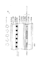
図16は、インクジェツトヘッドの複数のノズルを用いて、RGBストライプ配列のカラーフィルタの着色を行なう場合について、カラーフィルタの着色領域の一部と、それに対するインクジェットヘッドの状態を模式的に示した図である。
【0100】
通常カラーフィルタの同一色同士の画素ピッチと、一般のプリンタ等に使用されているインクジェットヘッドのノズルピッチは異なっているため、画素ピッチとノズルピッチとを一致させるようにする必要がある。
【0101】
本実施形態のインクジェットヘッドの場合、ノズルピッチが同一色同士の画素ピッチより小さいため、何本かおきのノズルからインクを吐出させて着色を行なうことになる。
【0102】
このとき、画素のピッチとノズルピッチの倍数が合わない場合ヘッドを傾けて配置する方法を用いることが一般的に知られている。
【0103】
図16のようにカラーフィルタの着色領域に対しインクジェットヘッド55b,55c,55dを斜めに傾けて配置し、さらに4ノズルおきにインクを吐出させるように設定している。
【0104】
このとき、インクジェットヘッド55b,55c,55dは、ぞれぞれ、R,G,Bを着色するインクジェットヘッドを示し、各色の画素を着色可能なように相対的に配置されている。
【0105】
図17乃至図21は、このインクジェットヘッドに対し、回復ユニット230によりワイピング方向を変えてワイピングを繰り返した際の着弾位置のずれを比較して模式的に示す図である。
【0106】
着弾位置を示す模式図に関しては、説明を容易にするため、赤色インクジェットヘッド55bにより着色を行なった場合について示してあるが、他の色に関しても同様のことが言える。
【0107】
図17は初期の着弾位置(着弾点)を模式的に示す図である。図中のラインMは、インクの着弾目標の線であり、ここではインクが目標着弾線(目標位置)に着弾しているため着弾位置のズレは発生していない。
【0108】
図17の場合、インクジェットヘッド55bにより吐出されたインクは着色画素内の所定の位置に着弾し、カラーフィルターが不良となることはない。
【0109】
次に、図18に示すようにインクジェットヘッド55に対し、回復ユニット230のブレードをA方向に動かし、ワイピングを繰り返した場合、着弾位置のずれは、図19のよう発生する。即ち、インクの着弾点のズレが、ワイピング方向と同じ方向に発生するのである。この場合、インクジェットヘッド55bにより吐出されたインクは画素をはみ出して着弾する。このため隣接する他色の画素に接触してしまい混色を引き起こし出来上がったカラーフィルターは不良となってしまう。尚、図19のラインNはインクの着弾目標の線であり、ここではインクドットA・インクドットB・インクドットC・インクドットD・インクドットE・インクドットFのうち、インクドットF以外のインクドットの着弾位置が目標着弾線に着弾しておらず着弾位置のズレが発生している。そして、そのズレ方向は同一色の画素が並ぶ方向とは異なっているため、隣接する異なる色の画素にインクが入り込んでしまい、混色が発生してしまう。
【0110】
一方、図20のように、インクジェットヘッドに対し回復ユニット230をB方向、すなわち同一色の画素の並び方向に沿った方向にブレードを動かした場合、着弾位置のずれは図21のように発生する。即ち、インクの着弾点のズレが、ワイピング方向と同じ方向に発生するのである。この場合、同一色の画素が並ぶ方向に沿った方向とワイピング方向とが一致しているので、ワイピング方向にインクの着弾点がずれたとしても、ずれたインクが隣接画素と接触することはなく、その結果、他色との混色の発生を低減させることができる。尚、図21のラインLはインクの着弾目標の線であり、ここではインクドットH・インクドットI・インクドットJ・インクドットK・インクドットL・インクドットMのうち、インクドットM以外のインクドットの着弾位置が目標着弾線に着弾しておらず着弾位置のズレが発生している。しかしながら、そのズレ方向は同一色の画素が並ぶ方向とは同じであるため、ズレが発生したとしても同じ色の画素にインク入り込むだけであるので混色が発生することはない。
【0111】
さらに、図26のように回復ユニット230を配置(インクジェットヘッド55に対してブレード232が斜めになるように配置)し、同様にB方向、同一色の画素の並び方向にブレードを動作させた場合もインクの着弾位置のずれは、図21のように発生する。
【0112】
このように、回復ユニット230内のブレード232の配置と、インクジェットヘッド55の配置との相対的な位置関係は特に限定されるものではない。ブレードの動作方向(ワイピング方向)が同一色の画素が並ぶ方向と同一であり、インクジェットヘッドのノズル面を拭き取ることが可能であれば問題はない。
【0113】
さらにインクジェットヘッドのノズル面をきれいに拭くことができ、かつ、他の色のインクがワイピングによりインクジェットヘッドのノズル面に付着することがなければ、図27のようにブレードを1つだけ配置する回復ユニット230を用いた構成にすることも可能である。
【0114】
次に、インクジェットヘッドの吐出口面の状態の変化について、模式図を用いて詳細に説明する。図28は、インクジェットヘッドの吐出口付近を拡大した模式図である。
【0115】
図28(a)は吐出口付近の初期の状態を示した図である。図28(a)から分かるように初期の状態において、インク吐出口の周辺部を含む吐出口面は完全に保護膜(保護部材)で覆われており、傷や膜剥れ等300は発生していない。
【0116】
尚、ヘッドの吐出口面を被複する保護膜としては、撥水性を有していることが好ましい。即ち、撥水膜(撥水部材)600により吐出口面を覆うことが好ましいのである。そこで本実施形態では、吐出口面が撥水膜で覆われているヘッドを用いている。また、初期の状態とは、ワイピング動作を1回も行っていないときの状態、もしくは傷や膜剥れ等が発生しない程度の回数しかワイピング動作を実行していないときの状態のことをさす。
【0117】
尚、傷部分や膜剥れ部分は、撥水部材の撥水性機能(撥水効果)が低下した部分であるので、撥水性低下部ということができる。また、保護部材の保護機能が低下した部分でもあるので、保護機能低下部ということもできる。また、傷部分や膜剥れ部分は、撥水部材あるいは保護部材に欠損が生じた部分でもあるため欠損部ということもでき、さらに撥水部材あるいは保護部材の磨耗した部分であるため磨耗部ということもできる。また、この撥水部材あるいは保護部材は、少なくとも吐出口の周辺(周囲)部分を被覆していれば良く、必ずしも吐出口面の全域を被覆している必要はないが、吐出口面全部を被覆していることが好ましい。
【0118】
図28(b)は、x方向にワイピング動作を繰り返した後の、インク吐出口周辺部を含む吐出口面の状態を示した図である。ワイピング動作を繰り返すことにより、インク吐出口の周辺部の撥水膜600に傷や膜剥れ部分300が発生する。
【0119】
図28(c)は、さらにx方向にワイピング動作を繰り返した後の、インク吐出口の周辺部を含む吐出口面の状態を示した図である。さらにワイピング動作を繰り返したことにより、吐出口面を覆っている撥水膜600の傷や膜剥れは、図28(b)の状態に比べてさらに大きくなっている。また、傷や膜剥れは単に大きくなるのではなく、規則性をもって大きくなっている。つまり、撥水膜の傷や膜剥れは、ワイピング方向(x方向)と同一方向に大きくなっていくのである。
【0120】
このように撥水膜に発生する傷や膜剥れは、ワイピングの回数の増加に伴ってワイピング方向に大きくなっていくのである。即ち、ワイピング動作を繰り返していくうちに、撥水膜の傷や膜剥れはワイピング方向と同一方向に長く伸びていくのである。また、撥水膜の傷や膜剥れは吐出口面全域で均一に発生するのではなく、特にインク吐出口の周辺部分において発生しやすい傾向が見られる。
【0121】
上記のような傷や膜剥れが発生した場合、インク吐出口の周辺部では、ワイピング動作時もしくは動作後においてインクの拭き残しが発生しやすくなる。すると、インク吐出口から吐出されるインク滴はこの拭き残しインクの影響を受け、拭き残しインクの方に引きずられてしまう。拭き残しインクの方に引きずられるということは、拭き残しインクが存在する部分、すなわち傷部分や膜剥れ部分が存在する部分の方へ引きずられるということである。傷部分や膜剥れ部分はワイピング方向と同一方向に存在しているため、吐出インクもこの方向(ワイピング方向と同一方向)へ引きずられ、インク滴の飛翔方向もワイピング方向と同一方向によれる。この結果、インク滴の着弾位置がワイピング方向と同一方向にずれるのである。また、吐出口周辺部の傷や膜剥れが大きければ大きいほど、インクの拭き残し量も多くなり、それに伴ってインク着弾位置のズレ量も大きくなる。すなわち、ワイピング動作を繰り返すことにより、ワイピング方向と同一方向に傷や膜剥れが徐々に発生し、その傷や膜剥れが大きくなるに従い、インクの着弾位置もワイピング方向と同一方向にずれていくのである。
【0122】
次に、ワイピング動作を繰り返すことでインクの着弾位置にズレが発生するメカニズムについて、図29〜図34を用いて詳細に説明する。
【0123】
図29は、インクジェットヘッドの吐出口面の初期状態を示す図である。図30は初期状態におけるインク吐出口からのインク滴吐出時の状態を模式的に示す図であり、図31は図30で示すような吐出状態のインク滴の着弾位置を模式的に示した図である。
【0124】
図29(a)のように初期状態における吐出口面はインク吐出口の周辺部まで完全に撥水膜(撥水部材)600で覆われており、吐出口面に対するX方向のワイピング動作時もしくは動作後において、図29(b)に示されるようにインク吐出口周辺部での拭き残しインクは全く存在しない、もしくはほとんど存在しない。
【0125】
インク吐出口の周辺部の状態が図29(b)の状態にある任意のインク吐出口から吐出されるインク滴は、図30のようにインク吐出口の中心で切り離され吐出方向が変化することなく安定して吐出されていく。つまり、吐出口面に対し垂直方向にインクが吐出されていくのである。この場合、インク滴の着弾位置は図31のようになり、画素内の所定の位置に正確に着弾する。尚、図31のラインAはインクの着弾目標の線であり、ここではインクが目標着弾線(目標位置)に着弾しているため着弾位置のズレは発生していない。
【0126】
図32は、ヘッドの吐出口面に対しx方向にワイピング動作を繰り返したときの吐出口面の状態を示す図である。図32(a)のようにワイピング動作を繰り返すことにより、吐出口面を覆っている撥水膜(撥水部材)600にはワイピング方向と同一方向に傷や膜剥れ300が発生する。実際にワイピング動作を行なった後の吐出口面の状態は、図32(b)に示されるようにインク吐出口周辺部に発生した傷部分や膜剥れ部分にインクの拭き残りが生じることが多い。インク吐出口周辺の状態が図32(b)の状態にある任意のインク吐出口から吐出されるインク滴は、図33のようにインク吐出口より切り離される直前に拭き残しのインク(インク残り)500に引きずられ、インクの吐出方向が変化してしまう。即ち、吐出口面に対して垂直な方向とは異なる方向にインクが吐出されていくのである。この場合、インク滴の着弾位置は図34のようになり、ワイピング方向と同一方向、すなわちヘッドの吐出口面に生じた傷部分や膜剥れ部分と同一方向に着弾位置のズレが発生している。尚、図34のラインBはインクの着弾目標の線であり、ここではインクドットR・インクドットS・インクドットT・インクドットUのうち、インクドットRとインクドットUの着弾位置が目標着弾線に着弾しておらず着弾位置のズレが発生している。しかしながら、x方向に着弾位置がずれるだけなので、画素からインクがはみ出して混色が発生することはない。
尚、上記では、図28のX1方向(往方向)とX2方向(復方向)の両方向にワイピング部材を往復移動させることによりワイピング動作を行っている。このようにX1、X2の両方向にワイピングすることで、図28(c)に示されるように吐出口付近の両側(X1方向側とX2方向側)に欠損部300が生じることとなる。仮に、片方向のみにワイピング部材を移動させてワイピング動作を行うこととすると、吐出口付近の片側にのみ欠損部が発生しやすくなる。具体的には、X2からX1へ向けてワイピング部材を移動させてワイピング動作を行う場合、即ちワイピング方向をX1方向とする場合、図28(c)のV1部分(X1側の部分)に欠損部が発生しやすく、一方、X1からX2へ向けてワイピング部材を移動させてワイピング動作を行う場合、即ちワイピング方向をX2方向とする場合、図28(c)のV2部分(X2側の部分)に欠損部が発生しやすい。このように片方向のみでワイピング動作を行うと欠損部が片側にのみ発生しやすく、それに起因してヘッドの寿命が短くなってしまう。そこで、本実施形態では、ヘッドの寿命をより長くするために、両方向でワイピング動作を行っている。
【0127】
ここで、本実施形態のワイピング動作についてより詳しく説明する。本実施形態では、20枚毎にワイピング動作を行っており、まず、20枚目のカラーフィルタを製造した後に、ワイピング部材をX1方向へ移動させてワイピング動作(第1のワイピング動作)を行う。次に、40枚目のカラーフィルタを製造した後に、ワイピング部材をX2方向へ移動させてワイピング動作(第2のワイピング動作)を行う。その後は上記動作を繰り返していき、60、100、140、…枚目の製造後にはX1方向へワイピングし(第1のワイピング動作を行い)、80、120、160、…枚目の製造後にはX2方向へワイピングする(第2のワイピング動作を行う)。尚、上記説明では20枚毎にワイピング動作を行っているが、ワイピング動作の頻度はこれに限定されるものではなく、例えばカラーフィルタを1枚製造する度にワイピング動作を行ってもよいし、100枚製造する毎に行ってもよい。このように本実施形態では、カラーフィルタをN枚製造する毎にワイピング動作を行えばよく、N枚製造する毎にワイピング方向を往方向と復方向とに交互に切り換えればよいのである。また、本実施形態ではワイピング方向を交互に切り換えることには限定されず、例えば、20、40枚目の製造後にはX1方向へワイピングし、60、80枚目の製造後にはX2方向へワイピングし、100、120枚目の製造後にはX1方向へワイピングし、140、160枚目の製造後にはX2方向へワイピングするようにしてよい。つまり、本実形態では、往方向にワイピングする回数と復方向にワイピングする回数とが略均等になるようにすればよく、複数回のワイピング動作を行う度にワイピング方向を切り換えてもよいのである。
【0128】
以上のように、本実施形態では、N枚製造する毎にワイピング方向を切り換え、往方向にワイピングする回数と復方向にワイピングする回数とを略等しくすることで、ヘッドの寿命が長くなるようにしている。尚、ヘッドの寿命を長くする観点から両方向でワイピング動作を行うことが好ましいが、本実施形態では片方向のみでワイピング動作を行ってもよい。
【0129】
また、本実施形態では、図16及び図20に示すように、同一色に着色される画素ピッチ(画像間隔)と、走査方向と略直交する方向における、使用するノズルのピッチ(使用ノズルの間隔)とが一致するように、インクジェットヘッドを走査方向に対してある角度だけ傾け、ヘッドを傾けたままの状態で着色を行っている。そして、ヘッドをある角度だけ傾けたまま状態で、同一色の画素が並ぶ方向に沿った方向(図20のB方向)にワイピング動作を行っている。ここで、仮に、傾いているヘッドを元の状態を戻してしからワイピング動作を行うこととすると、再びヘッドを傾けたときに欠損部の発生する方向と同一色に着色される画素が並ぶ方向とが一致せず、そのために混色を発生させてしまう。これに対し、本実施形態では、ヘッドを傾けたままの状態でワイピングを行っているので、欠損部の発生する方向と同一色に着色される画素が並ぶ方向とが一致するため、インクの着弾位置のズレ方向をB方向とすることができ、混色の低減を図ることができる。
【0130】
このように、インクジェットヘッドからカラーフィルタ基板上にインクを吐出して、所定の方向に延びる着色領域を形成してカラーフィルタを形成するに際し、ワイピング部材のワイピングの方向を上記所定の方向に沿った方向と同一にすることで、欠損部が発生する方向と所定の方向とが一致し、混色の低減を図ることができる。
【0131】
以上のように、ワイピング動作により吐出口面の撥水膜に傷や膜剥れが発生し、その傷や膜剥れに起因してインクの着弾位置がワイピング方向と同じ方向にずれるけれども、同一色の画素が並ぶ方向に沿った方向とワイピング方向とが一致しているため、インクの着弾位置がずれたとしても混色の原因となることはない。
【0132】
以下、本実施形態の具体的な実施例について説明する。
【0133】
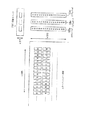
(実施例1)
本実施例で使用するインクジェットヘッドは、図22に示すように、一般のプリンタ用のヘッドで、隣接するノズルの間隔は70.5μm(360dpi)である。
【0134】
このインクジェットヘッドで12.1インチサイズSVGAのカラーフィルタ(縦600画素、横800画素を形成したRGBストライプ配列)の着色を行なう場合について説明する。
【0135】
まず、同一色同士の画素ピッチと、x方向のノズルピッチとを一致させるため、ヘッドを傾けて4ノズルおき(図22参照)に使用するように設定する。この例では、インクジェットヘッドのノズルの並び方向を、カラーフィルタの同一色画素の並び方向(Y方向)と略直交する方向(X方向)から少しすれた方向とし、図中Y方向にインクジェットヘッドを走査させながら着色を行う。即ち、この実施例1では、X方向に対して少し傾いた方向に吐出口が配列するようにしたヘッドを用い、そのヘッドを基板に対して相対的にY方向に走査させながら、同一色の複数の画素(同一色の画素列)がY方向に形成されるようにインクを吐出していくのである。
【0136】
このヘッドに対しワイピングブレードをヘッドと平行になるように配置した。
【0137】
次に、カラーフィルタを形成する。
【0138】
まず、所定の開口部を有するクロム(Cr)からなる12.1インチサイズSVGAタイプのブラックマトリクスを形成したガラス基板上に水性インク吸収性を有し、光照射あるいは、光照射と熱処理により光照射部分のインク吸収性が低下し、かつ、インクに対し撥水性を示す組成物材料(N−メチロールアクリルアミドとメタクリル酸メチルとヒドロキシエチルメタクリレートの3元共重合体10重量部とトリフェニルスルホニウムトリフラート0.4重量部からなる)をスピンコートで膜厚1.0μmとなるように塗布し、60℃で10分間のプリベークを行って樹脂組成物層を形成した。
【0139】
次いで、ブラックマトリクスより細いパターン形状のフォトマスクを介してUV(紫外線)ランプにて露光した。露光終了後、ホットプレートで110℃90秒間加熱して着色予定領域と混色防止領域(インク撥水性部分)となるインク撥水部を形成した。
【0140】
このようにして形成したガラス基板を図23に示すカラーフィルタ製造装置90のXYZθステージ52上にセットする。
【0141】
XYZθステージ52を走査させインクジェットヘッド55b,55c,55dにより着色を行なう。
【0142】
さらにインクミスト等がインクジェットヘッドのノズル面に付着してきた場合に、回復ユニット230を動作させワイピングを行なう。この時ブレードは、同一色の画素並び方向と同じ方向(すなわち図23上でX方向)に動作させる。
【0143】
上記の方法で着色を行なった基板を、90℃で10分間インク乾燥を行い、さらに230℃30分間の加熱処理により樹脂組成物層を完全に硬化させてカラーフィルタを作成した。
【0144】
このようにしてカラーフィルタの製造を繰り返し行なった。このとき、インクジェットヘッドから吐出されたインクの着弾位置のずれを測定したところ、初期の状態に対し異なる色の画素が並ぶ方向(図23のY方向)でのインク着弾のズレは、5μm以内であった。一方、カラーフィルタの同一色の画素が並ぶ方向(図23のX方向)でのインク着弾点のズレは10〜30μmであった。
【0145】
しかしながら、混色が発生することはなく、安定してカラーフィルタを作成することが可能であった。
【0146】
(実施例2)
実施例1と同様に、使用するインクジェットヘッドは、図24に示すように一般のプリンタ用のヘッドで、隣接するノズルの間隔は70.5μm(360dpi)である。
【0147】
このインクジェットヘッドで12.1インチサイズSVGAのカラーフィルタ(縦600画素、横800画素を形成したRGBストライプ配列)の着色を行なう場合について説明する。
【0148】
図24は、本実施例におけるカラーフィルタの着色領域の一部と、それに対するインクジェットヘッドの配置状態を模式的に示した図である。この例では、インクジェットヘッドのノズルの並び方向を、カラーフィルタの同一色画素の並び方向と一致させ、図中y方向にインクジェットヘッドを走査させながら着色を行う。即ち、この実施例2では、吐出口がx方向に配列したヘッドを用い、そのヘッドを基板に対して相対的にY方向に走査させながら、同一色の複数の画素(同一色の画素列)がx方向に形成されるようにインクを吐出していくのである。
【0149】
また、インクジェットヘッドに対しワイピングブレードをヘッドと直角になるように配置した。
【0150】
次に、カラーフィルタを形成する。
【0151】
まず、インクジェットヘッドを図中y方向に走査して、着色部を形成したガラス基板にインクジェットヘッド55b,55c,55dにより着色を行なう。
【0152】
着色を繰り返し、インクミスト等がインクジェットヘッドのノズル面に付着してきた場合に、回復ユニット230を動作させワイピングを行なう。この時ブレードは、同一色の画素が並ぶ方向と同じ方向(すなわち図24上でx方向)に動作させる。
【0153】
上記の方法で着色を行なった基板を、実施例1と同様の手順により樹脂組成物層を完全に硬化させてカラーフィルタを作成した。
【0154】
このようにしてカラーフィルタの製造を繰り返し行なった。このとき、インクジェットヘッドから吐出されたインクの着弾位置のずれを測定したところ、初期の状態に対し異なる色の画素が並ぶ方向(図24上のy方向)での着弾点のズレは5μm以内であった。また、カラーフィルターにおける同一色の画素が並ぶ方向(図24上でx方向)でのインク着弾点のズレは10〜30μmであった。
【0155】
しかしながら、混色が発生することはなく、安定してカラーフィルタを作成することが可能であった。
【0156】
(実施例3)
実施例1および実施例2と同様に、使用するインクジェットヘッドは図35に示すような一般のプリンタ用のヘッドで、隣接する吐出口の間隔は70.5μm(360dpi)である。
【0157】
このインクジェットヘッドを用いて、12.1インチサイズSVGAのカラーフィルタ(縦600画素、横800画素のRGBストライプタイプ配列)の着色を実施例1および実施例2とは異なる製造方法により行なう場合について説明する。
【0158】
図35は、本実施例におけるカラーフィルタの着色領域の一部と、それに対するインクジェットヘッドの配置状態を模式的にあらわした一例を示す図である。本実施例では、インクジェットヘッドの吐出口の並び方向を、カラーフィルタの同一色の画素の並び方向と一致させ、図のy方向にインクジェットと基板とを相対的に走査させながら着色を行なう。即ち、この実施例3では、吐出口がx方向に配列したヘッドを用い、そのヘッドを基板に対して相対的にy方向に走査させながら、同一色の複数の画素(同一色の画素列)がx方向に形成されるようにインクを吐出していくのである。
【0159】
また、インクジェットヘッドに対しワイピングブレードをヘッドと直角となるように配置した。
【0160】
次に、実際にカラーフィルタを形成していく場合について説明する。
【0161】
まず、ガラス基板に黒色顔料レジスト<新日鐵化学(株)製BK−739P>をスピンコート法により塗布した。次いで、インクを着色する部分を遮光するフォトマスク(不図示)を用いて、このフォトマスクを介してパターン露光し、エッチング処理によりレジストの一部を除去し着色部を形成した。さらに、90℃10分間のプリベークを行い、厚さ1.0μmのブラックマトリクス基板(BM基板)を形成した。なお、ブラックマトリクス間に形成された凹部のサイズは、290μm×90μmであった。
【0162】
このようにして形成したBM基板(ガラス基板)に対し、水、有機溶剤、メラミン樹脂及び顔料を含む熱硬化型の顔料インクをインクジェットヘッド55b、55c、55dから吐出して、基板上にR、G、Bのパターンを着色した。
【0163】
着色動作を繰り返していくうちに、インクミスト等がインクジェットヘッドの吐出口面に付着してきた場合に、回復ユニット230を動作させて吐出口面のワイピングを行った。このときブレードは、同一色の画素並び方向と同方向(すなわち図35のx方向)に動作させる。
【0164】
上記の方法で着色を行なった基板を、90℃10分間、さらに230℃30分間の熱処理によりインクを完全に硬化させた。さらに保護層を形成してカラーフィルタを作成した。
【0165】
このようにしてカラーフィルタの製造を繰り返し行なった。このとき、インクジェットヘッドから吐出されたインクの着弾位置のズレを測定したところ、初期の状態に対し異なる色の画素が並ぶ方向(y方向)でのインク着弾点のズレは5μm以内であった。また、カラーフィルタにおける同一色の画素が並ぶ方向(X方向)でのインク着弾点のズレは10〜30μmであった。
【0166】
しかしながら、混色が発生することはなく、安定してカラーフィルタを作成することが可能であった。
【0167】
(比較例1)
実施例1〜3と同様に、使用するインクジェットヘッドは図36に示すように一般のプリンタ用ヘッドで、隣接する吐出口の間隔は70.5μm(360dpi)である。このインクジェットヘッドを用い、12.1インチサイズSVGAのカラーフィルタ(縦600画素、横800画素のRGBストライプタイプ配列)の着色を行なう場合について説明する。
【0168】
図36は、本比較例におけるカラーフィルタの着色領域の一部と、それに対するインクジェットヘッドの配置状態を模式的にあらわした一例を示す図である。
【0169】
本比較例では、インクジェットヘッドの吐出口の並び方向をカラーフィルタの同一色の画素の並び方向と一致させ、図中y方向にインクジェットを相対的に走査させながら着色を行なう。即ち、この比較例では、吐出口がx方向に配列したヘッドを用い、そのヘッドを基板に対して相対的にy方向に走査させながら、同一色の複数の画素(同一色の画素列)がx方向に形成されるようにインクを吐出していくのである。
【0170】
また、インクジェットヘッドに対しワイピングブレードをヘッドと平行となるように配置した。
【0171】
次に、実際にカラーフィルタを形成していく場合について説明する。実施例3と同様の方法によりブラックマトリクスを形成したBM基板(ガラス基板)に対し、水、有機溶剤、メラミン樹脂及び顔料を含む熱硬化型の顔料インクをインクジェットヘッド55b、55c、55dから吐出して、基板上にR、G、Bのパターンを着色した。
【0172】
この着色動作を繰り返していくうちに、インクミスト等がインクジェットヘッドの吐出口面に付着してきた場合に、回復ユニット230を動作させて吐出口面のワイピングを行なう。このときブレードは、同一色の画素並び方向と直角方向(すなわち図36のy方向)に動作させる。
【0173】
上記の方法により着色を行なった基板を、実施例3と同様の手順によりインクを完全に硬化させカラーフィルタを形成した。
【0174】
このようにしてカラーフィルタの製造を繰り返し行なった。このとき、インクジェットヘッドから吐出されたインクの着弾位置のズレを測定したところ、初期の状態に対し同一色の画素が並ぶ方向(図36のx方向)でのインク着弾点のズレは5μm以内であった。また、異なる色の画素が並ぶ方向(図36のy方向)でのインク着弾点のズレは10〜30μmであった。
【0175】
隣接する異なる色の画素間の幅は約15μmであるため、着弾位置が約15μm以上ずれた部分では混色が発生しカラーフィルタは不良となってしまった。
【0176】
以上説明したように、上記の実施形態によれば、回復ユニットによるヘッドのワイピング方向を、同一色の画素の並び方向と一致させることにより、ワイピングを繰り返しても異なる色の画素間での混色を起きにくくすることができる。
【0177】
なお、本発明は、その主旨を逸脱しない範囲で、上記実施形態を修正又は変形したものに適用可能である。
【0178】
例えば、近年TFTアレイ側にカラーフィルタを設けたパネルも存在するが、本明細書で定義しているカラーフィルタは、色材により着色された被着色体であり、TFTアレイ側にあるか否かにかかわらず、どちらも包含する。
【0179】
本発明は、上記実施形態に限定されるものではなく、本発明の趣旨の範囲で種々に変更して適用することが可能である。
【0180】
本発明は、たとえば、EL(エレクトロルミネッセンス、electroluminesence表示素子の製造方法や製造装置等にも適用可能である。EL表示素子は、蛍光性の無機および有機化合物を含む薄膜を、陰極と陽極とで挟んだ構成を有し、前記薄膜に電子および正孔(ホール)を注入して再結合させることにより励起子を生成させ、この励起子が失活する際の蛍光或いは燐光の放出を利用して発光させる素子である。こうしたEL表示素子に用いられる蛍光性材料のうち、赤、緑および青色の発光色を呈する材料を本発明の製造装置を用いて、TFT等の素子基板上にインクジェット法によりパターニングすることで、自発光フルカラーEL表示素子を製造することができる。本発明の範囲にはこのようなEL表示素子、該表示素子の製造方法及びその製造装置等をも含むものである。
【0181】
本発明の製造装置は、EL材料が付着しやすいように、樹脂レジスト、画素電極および下層となる層の表面に対し、プラズマ処理、UV処理、カップリング処理等の表面処理工程を実行するための手段を有するものであってもよい。
本発明の製造方法を用いて製造したEL表示素子は、セグメント表示や全面同時発光の静止画表示等のローインフォメーション分野にも利用できるし、点・線・面形状をもった光源としても利用することができる。さらに、パッシブ駆動の表示素子をはじめ、TFT等のアクティブ素子を駆動に用いることで、高輝度で応答性の優れたフルカラー表示素子を得ることが可能である。
【0182】
以下に、本発明により製造される有機EL素子の一例を示す。図37は有機EL素子の積層構造断面図である。図37に示す有機EL素子は、透明基板3001、隔壁(仕切り部材)3002、発光層3003、透明電極3004および金属層3006を備えている。また、3007は、透明基板3001と透明電極3004とから構成される部分を示しており、これを駆動基板と呼ぶ。
【0183】
透明基板3001としては、EL表示素子としての透明性や機械的強度等の必要特性を有していれば特に限定されるものではなく、例えば、ガラス基板やプラスチック基板等の光透過性の基板が適用可能である。
【0184】
隔壁(仕切り部材)3002は、液体付与ヘッドから発光層3003となる材料を付与するに際し隣接する画素間で該材料が混合しないように画素と画素の間を隔離するための機能を有するものである。すなわち、隔壁3002は混色防止壁として機能するのである。また、この隔壁3002を透明基板3001上に設けることにより、基板上には複数の凹部(画素領域)が形成される。尚、隔壁3002は、該材料に対して親和性の異なる多層構造であっても問題無い。
【0185】
発光層3003は、電流を流すことにより発光する材料、例えばポリフェニレンビニレン(PPV)等公知の有機半導体材料を使用して、十分な光量が得られる厚み、例えば0.05μm〜0.2μm程度積層して構成される。発光層3003はインクジェット方式などの方法によって薄膜材料液(自発光材料)を隔壁3002で囲まれる凹部に充填し加熱処理することで形成される。カラー有機EL素子を形成する場合には、赤、緑または青などの異なる発光色を有する発光層を形成する必要がある。したがって、隣接する領域に異なる発光層を形成することが好ましく、任意の位置に異なる薄膜材料液を吐出できるインクジェット方式で発光層を形成する方法は非常に有効な方法である。
【0186】
透明電極3004は、導電性がありかつ光透過性のある材料、例えばITO等により構成されている。透明電極3004は、画素単位で発光させるために、画素領域ごとに独立して設けられている。
【0187】
金属層3006は、導電性のある金属材料、例えばアルミニウムリチウム(Al−Li)を0.1μm〜1.0μm程度積層して構成される。金属層3006は、透明電極3004に対向する共通電極として作用するように形成されている。
【0188】
駆動基板3007は、図示しない薄膜トランジスタ(TFT)、配線膜および絶縁膜等が多層に積層されており、金属層3006および各透明電極3004間に画素単位で電圧を印加可能に構成されている。駆動基板3007は公知の薄膜プロセスによって製造される。
【0189】
上記のような層構造を有する有機EL素子において、透明電極3004と金属層3006との間に電圧が印加された画素領域では、発光層3003に電流が流れ、エレクトロルミネッセンス現象を生じ、透明電極3004および駆動基板3001を通して光が射出されるようになっている。
本例の方法によれば、簡便な工程でフルカラーEL素子を形成することが可能となる。
【0190】
尚、本発明では、画素部領域に、表示に用いられるための材料を付与することで表示部を形成しており、カラーフィルタであれば着色部が上記表示部に相当し、EL素子であれば発光部が上記表示部に相当する。上記着色部や発光部を含む表示部は、情報の表示のために用いられる部分であり、視覚的に色を認識するための部分でもある。
【0191】
また、カラーフィルタの着色部やEL素子の発光部は、色を生じさせる(色が発さられる)部分でもあるため発色部というもできる。例えば、カラーフィルタの場合、バックライトによる光が着色部を通過してRGBの光が発せられ、また、EL素子の場合、発光部が自発光することによりRGBの光が発せられる。
また、インクや自発光材料は、上記発色部を形成するための材料であるので、発色を生じさせる材料ということもできる。またインクや自発光材料は、液体であるので、総称して液体材料ということもできる。また、インクや自発光材料は、表示に用いられる表示部を形成するための材料でもある。
【0192】
また、上記では、カラーフィルタを製造するに際し、画素領域において混色が発生することを起こりにくくすることができると説明した。一方、EL素子の製造の場合、画素領域において複数の自発光材料が混ざり合うことを起こりにくすることができる。
【0193】
以上のように本発明は、隔壁により囲まれる複数の凹部に材料を充填して複数の表示部が形成されたパネル、例えばカラーフィルタ・EL素子等を含むカラー表示装置に使用されるパネル(表示用素子)の製造に適用可能である。尚、この表示装置用のパネルは、上記カラーフィルタ及びEL表示素子に限定されるものでなく、基板上の画素領域に液体材料を充填していくことにより形成されたパネルであって、表示装置に利用できるパネル全般を含むものである。
【0194】
本発明は、特にインクジェット記録方式の中でも、インク吐出を行わせるために利用されるエネルギーとして熱エネルギーを発生する手段(例えば電気熱変換体やレーザ光等)を備え、前記熱エネルギーによりインクの状態変化を生起させる方式のプリント装置について説明したが、かかる方式によれば記録の高密度化、高精細化が達成できる。
【0195】
その代表的な構成や原理については、例えば、米国特許第4723129号明細書、同第4740796号明細書に開示されている基本的な原理を用いて行うものが好ましい。この方式はいわゆるオンデマンド型、コンティニュアス型のいずれにも適用可能であるが、特に、オンデマンド型の場合には、液体(インク)が保持されているシートや液路に対応して配置されている電気熱変換体に、記録情報に対応していて膜沸騰を越える急速な温度上昇を与える少なくとも1つの駆動信号を印加することによって、電気熱変換体に熱エネルギーを発生せしめ、記録ヘッドの熱作用面に膜沸騰を生じさせて、結果的にこの駆動信号に1対1で対応した液体(インク)内の気泡を形成できるので有効である。この気泡の成長、収縮により吐出用開口を介して液体(インク)を吐出させて、少なくとも1つの滴を形成する。この駆動信号をパルス形状をすると、即時適切に気泡の成長収縮が行われるので、特に応答性に優れた液体(インク)の吐出が達成でき、より好ましい。
【0196】
このパルス形状の駆動信号としては、米国特許第4463359号明細書、同第4345262号明細書に記載されているようなものが適している。なお、上記熱作用面の温度上昇率に関する発明の米国特許第4313124号明細書に記載されている条件を採用すると、さらに優れた記録を行うことができる。
【0197】
記録ヘッドの構成としては、上述の各明細書に開示されているような吐出口、液路、電気熱変換体の組み合わせ構成(直線状液流路または直角液流路)の他に熱作用面が屈曲する領域に配置されている構成を開示する米国特許第4558333号明細書、米国特許第4459600号明細書を用いた構成も本発明に含まれるものである。加えて、複数の電気熱変換体に対して、共通するスロットを電気熱変換体の吐出部とする構成を開示する特開昭59−123670号公報や熱エネルギーの圧力波を吸収する開口を吐出部に対応させる構成を開示する特開昭59−138461号公報に基づいた構成としても良い。
【0198】
さらに、記録装置が記録できる最大記録媒体の幅に対応した長さを有するフルラインタイプの記録ヘッドとしては、上述した明細書に開示されているような複数記録ヘッドの組み合わせによってその長さを満たす構成や、一体的に形成された1個の記録ヘッドとしての構成のいずれでもよい。
【0199】
加えて、装置本体に装着されることで、装置本体との電気的な接続や装置本体からのインクの供給が可能になる交換自在のチップタイプの記録ヘッド、あるいは記録ヘッド自体に一体的にインクタンクが設けられたカートリッジタイプの記録ヘッドを用いてもよい。
【0200】
また、本発明の記録装置の構成として設けられる、記録ヘッドに対しての回復手段、予備的な補助手段等を付加することは本発明の効果を一層安定にできるので好ましいものである。これらを具体的に挙げれば、記録ヘッドに対しての加圧あるいは吸引手段、電気熱変換体あるいはこれとは別の加熱素子あるいはこれらの組み合わせによる予備加熱手段、記録とは別の吐出を行う予備吐出モードを行うことも安定した記録を行うために有効である。
【0201】
以上説明した本発明実施形態においては、インクを液体として説明しているが、室温やそれ以下で固化するインクであっても、室温で軟化もしくは液化するものを用いても良く、使用記録信号付与時にインクが液状をなすものであればよい。
【0202】
加えて、積極的に熱エネルギーによる昇温をインクの固形状態から液体状態への状態変化のエネルギーとして使用せしめることで積極的に防止するため、またはインクの蒸発を防止するため、放置状態で固化し加熱によって液化するインクを用いても良い。いずれにしても熱エネルギーの記録信号に応じた付与によってインクが液化し、液状インクが吐出されるものや、記録媒体に到達する時点では既に固化し始めるもの等のような、熱エネルギーの付与によって初めて液化する性質のインクを使用する場合も本発明は適用可能である。このような場合インクは、特開昭54−56847号公報あるいは特開昭60−71260号公報に記載されるような、多孔質シート凹部または貫通孔に液状または固形物として保持された状態で、電気熱変換体に対して対向するような形態としてもよい。本発明においては、上述した各インクに対して最も有効なものは、上述した膜沸騰方式を実行するものである。
【0203】
【発明の効果】
以上説明したように、本発明によれば、インクジェットヘッドのノズル面(吐出口面)のワイピングを繰り返しても、画素領域において複数の材料が混ざり合うことを起こりにくくすることができる。
【図面の簡単な説明】
【図1】カラーフィルタの製造装置の一実施形態の構成を示す概略図である。
【図2】カラーフィルタの製造装置の動作を制御する制御部の構成を示す図である。
【図3】カラーフィルタの製造装置に使用されるインクジェットヘッドの構造を示す図である。
【図4】カラーフィルタの製造方法を示した図である。
【図5】カラーフィルタの製造工程を示した図である。
【図6】一実施形態のカラーフィルタを組み込んだカラー液晶表示装置の基本構成の一例を示す断面図である。
【図7】一実施形態のカラーフィルタを組み込んだカラー液晶表示装置の基本構成の他の例を示す断面図である。
【図8】一実施形態のカラーフィルタを組み込んだカラー液晶表示装置の基本構成のさらに他の例を示す断面図である。
【図9】液晶表示装置が使用される情報処理装置を示した図である。
【図10】液晶表示装置が使用される情報処理装置を示した図である。
【図11】液晶表示装置が使用される情報処理装置を示した図である。
【図12】インクジェットヘッドのノズル面を示す模式図である。
【図13】インクジェットヘッドの回復ユニットの構成を示す模式図である。
【図14】インクジェットヘッドから吐出されたインクの着弾位置のずれを示す図である。
【図15】インクジェットヘッドから吐出されたインクの着弾位置のずれを示す図である。
【図16】カラーフィルタの着色画素とインクジェットヘッドのノズルの関係を示す図である。
【図17】インクジェットヘッドから吐出されたインクの初期状態での着弾位置を示す図である。
【図18】カラーフィルタの着色画素とインクジェットヘッド、回復ユニットの動作方向の関係を示す図である。
【図19】図18の構成でワイピングを繰り返した際のインクジェットヘッドから吐出されたインクの着弾位置を示す図である。
【図20】カラーフィルタの着色画素とインクジェットヘッド、回復ユニットの動作方向の関係を示す図である。
【図21】図20の構成でワイピングを繰り返した際のインクジェットヘッドから吐出されたインクの着弾位置を示す図である。
【図22】カラーフィルタの着色画素とインクジェットヘッドのノズルの関係を示す図である。
【図23】カラーフィルタの製造装置の一部を示す図である。
【図24】カラーフィルタの着色画素とインクジェットヘッド、回復ユニットの動作方向の関係を示す図である。
【図25】カラーフィルタの製造工程の他の例を示す図である。
【図26】インクジェットヘッドとブレードの位置関係を示す図である。
【図27】インクジェットヘッドとブレードの位置関係を示す図である。
【図28】インクジェットヘッド吐出口面の状態変化を示す模式図である。
【図29】インクジェットヘッドヘッドの吐出口面の初期状態を示す模式図である。
【図30】初期状態でのインクジェットヘッドのインク吐出状態を示す模式図である。
【図31】初期状態におけるインクジェットヘッドから吐出されたインクの着弾位置を示す模式図である。
【図32】ワイピングを繰り返したあとのインクジェットヘッドヘッドの吐出口面の状態を示す模式図である。
【図33】ワイピングを繰り返したあとのインクジェットヘッドのインク吐出状態を示す模式図である。
【図34】ワイピングを繰り返したあとのインクジェットヘッドから吐出されたインクの着弾位置を示す模式図である
【図35】カラーフィルタの着色画素とインクジェットヘッド、回復ユニットの動作方向の関係の一例を示す模式図である。
【図36】カラーフィルタの着色画素とインクジェットヘッド、回復ユニットの動作方向の関係の一例を示す模式図である。
【図37】 EL素子の構成を示す図である。
【図38】所定の方向に延びる着色領域を説明するための図である。
【符号の説明】
1 基板
2 ブラックマトリクス
3 樹脂組成物層
55 インクジェットヘッドユニット
55b,55c,55d インクジェットヘッド
90 カラーフィルタの製造装置
108 吐出口
230 回復ユニット
232 ブレード
300 傷や膜剥れ
500 インク残り[0001]
BACKGROUND OF THE INVENTION
The present invention relates to a display device panel manufacturing method and manufacturing apparatus for manufacturing a display device panel (display element) by coloring pixels on a substrate with a head, for example, a color television or a personal computer. The present invention relates to a color filter manufacturing method and manufacturing apparatus, a display device manufacturing method, a device including a display device, and the like.
[0002]
[Prior art]
With the rapid development of portable personal computers in recent years, the demand for liquid crystal displays, especially color liquid crystal displays, tends to increase. At the same time, there is a demand for cost reduction of the apparatus, and there is an increasing demand for cost reduction of a color filter having a relatively high cost ratio. Various methods have been tried to satisfy the required characteristics of the color filter and satisfy the above-mentioned requirements, but they are still insufficient. Each method will be described below.
[0003]
The most frequently used first method is the pigment dispersion method. In this method, first, a photosensitive resin layer in which a pigment is dispersed is formed on a substrate, and this is patterned to obtain a monochromatic pattern. Further, this process is repeated three times to obtain R, G, and B color filter layers.
[0004]
The second method is a staining method. In this method, a water-soluble polymer material that is a dyeing material is formed on a glass substrate, patterned into a certain shape by a photolithography process, and the resulting pattern is immersed in a dyeing bath to form a colored pattern. obtain. By repeating this three times, R, G, and B color filters are formed.
[0005]
There is an electrodeposition method as a third method. In this method, a transparent substrate is first patterned on a substrate. Next, the first color is electrodeposited by dipping in an electrodeposition coating solution containing a pigment, resin, electrolytic solution or the like. This process is repeated three times to form R, G, B colored layers, and finally fired.
[0006]
As a fourth method, there is a printing method. In this method, a pigment is dispersed in a thermosetting resin, R, G, and B are separately applied by repeating printing three times, and then the resin is thermally cured to form a colored layer. In any method, a protective layer is generally formed on the colored layer.
[0007]
The point common to the conventional methods is that the same process needs to be repeated three times in order to color the three colors R, G, and B, resulting in high costs. In addition, there is a problem that the yield decreases as the number of processes increases. Furthermore, in the electrodeposition method, the pattern shapes that can be formed are limited, so that it is difficult to apply to TFTs with the current technology. Also, the printing method is not suitable for forming a fine pitch pattern because of its poor resolution.
[0008]
[Problems to be solved by the invention]
In order to make up for these drawbacks, as a method of manufacturing a color filter using an ink jet, JP-A-59-75205, JP-A-63-235901, JP-A-1-217320, JP-A-4-123005, There are proposals such as 9-138306. Unlike the conventional method, these inks of R (red), G (green), and B (blue) are ejected from ink jet heads to predetermined positions on a light-transmitting substrate, and the ink is ejected onto the substrate. According to this method, the color layers of R, G, and B can be formed at once, and the amount of ink used is not wasted. Effects such as improvement of productivity and cost reduction can be obtained.
[0009]
When a color filter is manufactured using such an ink jet method, the nozzle surface (ejection port surface) of the ink jet head is stained with ink while the ink is repeatedly ejected. Therefore, the nozzle surface is periodically cleaned. There is a need.
[0010]
Conventionally, cleaning of the nozzle surface has been performed by wiping the nozzle surface of the inkjet head with a sponge-like wiping member having elasticity.
[0011]
At this time, it is common to perform cleaning by moving the wiping member in a direction in which the nozzles of the inkjet head are arranged or in a direction perpendicular to the nozzle row.
[0012]
Normally, by repeatedly wiping the nozzle surface of the inkjet head, fine scratches are gradually generated in the vicinity of the nozzle holes on the nozzle surface, or the water repellent effect of the water repellent part is reduced, and the ink is discharged from the inkjet head. The flying direction of the ink droplet changes slightly and the landing position shifts.
[0013]
Such a deviation in the landing position is a level that does not cause a problem in a general ink jet printer, but in coloring a high-definition pattern such as a color filter, it causes a color mixture with an adjacent coloring region, which is a big problem in reducing the yield. It was.
[0014]
Accordingly, the present invention has been made in view of the above-described problems, and an object of the present invention is to produce a color filter without reducing the yield even if the wiping of the nozzle surface (discharge port surface) of the inkjet head is repeated. Color filter manufacturing method and manufacturing apparatus, color filter manufactured by the manufacturing method, display device including the color filter, manufacturing method of the apparatus including the display device, and display panel manufacturing A method and manufacturing apparatus are provided.
[0015]
[Means for Solving the Problems]
In order to solve the above-described problems and achieve the object, the color filter manufacturing method according to the present invention includes an ejection port for ejecting ink.FormedBy discharging ink onto a substrate from an inkjet head having a discharge port surface and at least a peripheral portion of the discharge port covered with a water repellent member, a colored region extending in a predetermined direction is formed for each color. A method of manufacturing a color filter, comprising: wiping the discharge port surface with a wiping member for wiping the discharge port surface, wherein the wiping memberbyThe wiping direction is the same as the direction along the predetermined direction.
[0016]
The color filter manufacturing method according to the present invention includes an ink jet head and a substrate having a discharge port surface on which a discharge port for discharging ink is formed, and a peripheral part of the discharge port is covered with a water repellent member. Is a method of manufacturing a color filter in which a plurality of pixels formed of the same color ink are arrayed in the predetermined direction while being moved relative to each other in a predetermined direction. The interval between two pixels of the inkjet head and the interval between two ejection ports used among the plurality of ejection ports of the inkjet head in a direction orthogonal to the predetermined direction are the same with respect to the predetermined direction of the inkjet head. An adjustment step for adjusting the angle, and the substrate during the relative movement from the inkjet head while maintaining the angle adjusted in the adjustment step. Wiping the ejection port surface with a wiping member while maintaining the angle adjusted in the adjustment step, and the wiping direction of the wiping member is the predetermined direction It is characterized by being the same as the direction along.
[0017]
In addition, a method for manufacturing a liquid crystal panel according to the present invention is a method for manufacturing a liquid crystal panel including a color filter, the step of preparing a color filter manufactured by the above manufacturing method, and the prepared color filter. And a step of inserting a liquid crystal compound between the counter substrate and the counter substrate.
[0018]
The display device manufacturing method according to the present invention is a method for manufacturing a display device having a liquid crystal panel, the step of preparing the liquid crystal panel manufactured by the above manufacturing method, and the prepared liquid crystal panel. And a step of connecting an image signal supply means for supplying an image signal.
[0019]
In addition, the method for manufacturing a display device panel according to the present invention includes a liquid application having a discharge port surface on which a discharge port for discharging a liquid is formed, and a peripheral portion of the discharge port is covered with a water repellent member. A method for manufacturing a panel for a display device, in which a liquid crystal is applied from a head onto a substrate, the display panel extending in a predetermined direction and having a display unit used for display arranged, and for wiping the discharge port surface A step of wiping the discharge port surface with a wiping member is provided, and a wiping direction by the wiping member is the same as a direction along the predetermined direction.
[0020]
Further, the method for manufacturing a display device panel according to the present invention has a discharge port surface on which a discharge port for discharging a material used for display is formed, and at least a peripheral portion of the discharge port has a water-repellent surface. A method of manufacturing a panel for a display device by ejecting the material from a head covered with a member onto a substrate to form a display portion that extends in a predetermined direction and is used for display, and is formed of the same material The predetermined interval of the head is set so that the interval between the two display units to be coincided with the interval in the direction perpendicular to the predetermined direction of two discharge ports to be used among the plurality of discharge ports of the head. An adjusting step of adjusting an angle with respect to the direction of the liquid, and a step of wiping the discharge port surface with a wiping member while maintaining the angle adjusted in the adjusting step. The wiping direction by the material is the same as the direction along the predetermined direction.
[0021]
The color filter manufacturing apparatus according to the present invention includes an inkjet head having an ejection port surface on which ejection ports for ejecting ink are formed, and at least a peripheral portion of the ejection port is covered with a water repellent member. An apparatus for producing a color filter by ejecting ink onto a substrate and forming a colored region extending in a predetermined direction for each color, comprising a wiping member for wiping the ejection port surface, and the wiping The wiping direction by the member is the same as the direction along the predetermined direction.
[0029]
DETAILED DESCRIPTION OF THE INVENTION
Hereinafter, a preferred embodiment of the present invention will be described in detail with reference to the accompanying drawings.
[0030]
Note that the display device panel (display element) defined in the present invention has a display portion used for display. More specifically, the display device panel is a panel used in a display device including, for example, a color filter having a colored portion or an EL element having a light emitting portion formed of a self-luminous material. . In the case of a color filter, the colored portion corresponds to the display portion, and in the case of an EL element, the light emitting portion corresponds to the display portion. Further, the color filter defined in the present invention includes a colored portion and a base, and can obtain output light whose characteristics are changed with respect to input light. The base includes a substrate such as glass or plastic, and includes a shape other than a plate. The expression of the colored region extending in a predetermined direction in the color filter is as shown in FIG. 38 (a) when the pixels are long in a line, or as shown in (b), (c), and (d). This includes the case where one row is divided into a plurality of pixels. The colored region of the color filter can also be referred to as a region for visually recognizing a color. Furthermore, the ink jet head used for coloring in the present embodiment has a discharge port surface in which an ink discharge port is opened, and at least a peripheral portion of the opening of the discharge port is covered with a predetermined material. Further, since the ink jet head applies ink that is a colored liquid to the color filter substrate, it can also be called a liquid applying head.
[0031]
FIG. 1 is a schematic diagram showing the configuration of a color filter manufacturing apparatus using an ink jet method, and shows a state during the coloring process.
[0032]
In FIG. 1, 51 is an apparatus base, 52 is an XYZθ stage disposed on the
[0033]
The
[0034]
FIG. 2 is a configuration diagram of the control controller of the color
[0035]
58 is a controller for controlling the overall operation of the color
[0036]
Next, FIG. 3 is a diagram showing the structure of the inkjet head IJH used in the color
[0037]
In FIG. 3, the ink jet head IJH is generally configured by a
[0038]
The
[0039]
FIG. 4 is a diagram showing an example of manufacturing a color filter by an ink jet head.
[0040]
In the color filter of the present invention, a light-transmitting substrate is preferable as the
[0041]
On the
[0042]
In addition, as an ink jet method used in the present invention, a bubble jet using an electrothermal transducer as an energy generating element is used.(Registered trademark)A type, a piezo jet type using a piezoelectric element, or the like can be used, and a coloring area and a coloring pattern can be arbitrarily set.
[0043]
FIG. 5 is a diagram showing a manufacturing process of a color filter.
[0044]
A
[0045]
As the
[0046]
The
[0047]
Next, the
[0048]
The
[0049]
The thickness of the
[0050]
The
[0051]
The photomask 4 shown in the figure in this case is a case where the
[0052]
As shown in the figure, the
[0053]
The
[0054]
Each unexposed portion is surrounded by an
[0055]
In the present invention, as an ink jet system, a bubble jet type using an electrothermal transducer or a piezo jet type using a piezoelectric element can be used as an energy generating element, and the coloring area and coloring pattern can be arbitrarily set. it can.
[0056]
In the present invention, as the ink for coloring, both dye-based and pigment-based inks can be used. In addition, the ink is not limited to liquid at room temperature, but is ink that solidifies at room temperature or lower, and is softened at room temperature, or is liquid, or in the above inkjet method, the ink itself is 30 ° C. or higher and 70 ° C. or lower. In general, the temperature is adjusted within the above range to control the temperature of the ink so that the viscosity of the ink is within the stable ejection range. Therefore, the liquid in which the ink is in a liquid state when a use recording signal is applied is preferably used.
[0057]
Further, if necessary, the ink is dried, and heat treatment is performed to completely cure the entire
[0058]
As the
[0059]
(Second method)
FIG. 25 is a process diagram of the second method, and the same members as those in FIG. Moreover, (a)-(d) of FIG. 25 is a schematic diagram corresponding to the following process (a)-(d).
[0060]
Step (a)
First, a partition wall (partition member) is formed on the
[0061]
Step (b)
From the inkjet head 37, the
[0062]
The ink used in the present invention is a resin composition that is cured by applying energy and usually contains a colorant. As the colorant, a general dye or pigment can be used. For example, an anthraquinone dye, an azo dye, a triphenylmethane dye, a polymethine dye, or the like can be used as the dye.
[0063]
As the resin used for the ink, a resin that is cured by applying energy such as heat treatment or light irradiation is used. Specifically, a combination of a known resin and a crosslinking agent can be used as the thermosetting resin. For example, acrylic resin, melamine resin, hydroxyl group or carboxyl group-containing polymer and melamine, hydroxyl group or carboxyl group-containing polymer and polyfunctional epoxy compound, hydroxyl group or carboxyl group-containing polymer and fibrin reactive compound, epoxy resin and resole type resin, epoxy Examples thereof include resins and amines, epoxy resins and carboxylic acids or acid anhydrides, and epoxy compounds. Moreover, as a photocurable resin, a well-known thing, for example, a commercially available negative resist, is used suitably.
[0064]
Various solvents can be added to the ink. In particular, a mixed solvent of water and a water-soluble organic solvent is preferably used from the viewpoint of dischargeability in the ink jet system.
[0065]
In addition to the above components, surfactants, antifoaming agents, preservatives, and the like can be added to give desired properties as necessary, and commercially available water-soluble dyes can also be added. Can do.
[0066]
In addition, among the light or thermosetting resins described above, a solvent other than water or a water-soluble organic solvent may be used as long as it does not dissolve in water or a water-soluble organic solvent and can be stably discharged. In particular, when a monomer that is polymerized by light is used, a solventless type in which a dye is dissolved in the monomer may be used.
[0067]
Step (c)
The
[0068]
Step (d)
A
[0069]
6 to 8 are cross-sectional views showing a basic configuration of a color liquid
[0070]
The color liquid crystal display device (color liquid crystal display) according to the present invention is formed by combining the
[0071]
Further, as shown in FIG. 8, a colored portion may be formed on the
[0072]
An example in which such a liquid crystal display device is applied to an information processing device will be described with reference to FIGS. This information processing apparatus is manufactured by connecting image signal supply means for supplying an image signal to a liquid crystal display device having a color filter manufactured by using the manufacturing method according to the present invention.
[0073]
FIG. 9 is a block diagram showing a schematic configuration when the above liquid crystal display device is applied to an information processing apparatus having functions as a word processor, personal computer, facsimile apparatus, and copying apparatus.
[0074]
In the figure,
[0075]
[0076]
[0077]
[0078]
[0079]
Reference numeral 1811 denotes a keyboard unit for inputting document information and various commands.
[0080]
An
[0081]
FIG. 10 is a schematic overview of the information processing apparatus shown in FIG.
[0082]
In the figure,
[0083]
[0084]
When the information processing apparatus functions as a personal computer or a word processor, various types of information input from the keyboard unit 1811 are processed by the
[0085]
When functioning as a receiver of a facsimile apparatus, facsimile information input from a FAX transmission /
[0086]
When functioning as a copying apparatus, the original is read by the
[0087]
Note that the above-described information processing apparatus may be an integrated type in which an ink jet printer is built in the main body as shown in FIG. 11, and in this case, the portability can be further improved. In the figure, parts having the same functions as those in FIG. An apparatus having a display device as described above is: (1) First, a color filter is manufactured by the manufacturing method according to the present invention; (2) Next, a liquid crystal compound is filled between the color filter and the counter substrate. (3) Finally, an image signal supply means is connected to the display device.
[0088]
Next, FIG. 12 is a diagram showing a nozzle surface of an inkjet head having a plurality of nozzles.
[0089]
In this embodiment, the nozzle row direction and the nozzle row perpendicular direction are defined as shown in FIG.
[0090]
FIG. 13 is a configuration diagram showing the
[0091]
In FIG. 13,
[0092]
[0093]
As shown in FIG. 13, the
[0094]
In the present embodiment, the XY direction that is the operation direction of the
[0095]
14 and 15 are graphs showing the results of measuring the deviation of the landing position when the
[0096]
FIG. 14 is a graph showing the result of measuring the deviation of the landing position in the nozzle row perpendicular direction (wiping operation direction), and FIG. 15 is a graph showing the result of measuring the deviation of the landing position in the nozzle row direction.
[0097]
As can be seen from FIGS. 14 and 15, in the nozzle row perpendicular direction which is the wiping operation direction, the deviation of the landing position gradually increases as the number of wiping increases. On the other hand, when it opens in the nozzle row direction, even if the number of wiping increases, the deviation of the landing position hardly changes.
[0098]
From this, it is clear that the direction of wiping and the direction of deviation of the landing position are related, and it can be seen that the direction of occurrence of deviation of the landing position can be controlled by controlling the direction of wiping.
[0099]
FIG. 16 schematically shows a part of the colored region of the color filter and the state of the inkjet head with respect to the color filter of the RGB stripe arrangement using a plurality of nozzles of the inkjet head. FIG.
[0100]
Since the pixel pitch of the same color of the normal color filter is different from the nozzle pitch of an inkjet head used in a general printer or the like, it is necessary to match the pixel pitch with the nozzle pitch.
[0101]
In the case of the inkjet head of this embodiment, since the nozzle pitch is smaller than the pixel pitch of the same color, coloring is performed by ejecting ink from several nozzles.
[0102]
At this time, it is generally known to use a method in which the head is inclined when the pixel pitch and the multiple of the nozzle pitch do not match.
[0103]
As shown in FIG. 16, the inkjet heads 55b, 55c, and 55d are arranged obliquely with respect to the colored region of the color filter, and the ink is set to be discharged every four nozzles.
[0104]
At this time, the inkjet heads 55b, 55c, and 55d indicate inkjet heads that color R, G, and B, respectively, and are relatively disposed so that the pixels of each color can be colored.
[0105]
FIGS. 17 to 21 are diagrams schematically showing a difference in landing position when the wiping direction is changed by the
[0106]
The schematic diagram showing the landing position shows the case where coloring is performed by the
[0107]
FIG. 17 is a diagram schematically showing an initial landing position (landing point). A line M in the figure is an ink landing target line, and since the ink has landed on the target landing line (target position), there is no deviation in the landing position.
[0108]
In the case of FIG. 17, the ink ejected by the
[0109]
Next, as shown in FIG. 18, when the blade of the
[0110]
On the other hand, when the blade is moved in the B direction, that is, in the direction along the arrangement direction of pixels of the same color with respect to the inkjet head as shown in FIG. 20, the deviation of the landing position occurs as shown in FIG. . That is, the deviation of the ink landing point occurs in the same direction as the wiping direction. In this case, since the direction along the direction in which pixels of the same color are aligned and the wiping direction match, even if the ink landing point is shifted in the wiping direction, the shifted ink does not come into contact with the adjacent pixel. As a result, the occurrence of color mixing with other colors can be reduced. The line L in FIG. 21 is a target line for ink landing. Here, the ink dots H, ink dots I, ink dots J, ink dots K, ink dots L, and ink dots M other than the ink dots M are shown. The landing position of the ink dot has not landed on the target landing line, and the landing position has shifted. However, since the misalignment direction is the same as the direction in which pixels of the same color are arranged, even if the misalignment occurs, only ink enters the pixels of the same color, so no color mixing occurs.
[0111]
Furthermore, when the
[0112]
Thus, the relative positional relationship between the arrangement of the
[0113]
Further, if the nozzle surface of the inkjet head can be wiped cleanly and no other color ink adheres to the nozzle surface of the inkjet head by wiping, a recovery unit in which only one blade is arranged as shown in FIG. A configuration using 230 is also possible.
[0114]
Next, changes in the state of the ejection port surface of the inkjet head will be described in detail with reference to schematic diagrams. FIG. 28 is an enlarged schematic view of the vicinity of the ejection port of the inkjet head.
[0115]
FIG. 28A is a diagram showing an initial state near the discharge port. As can be seen from FIG. 28A, in the initial state, the discharge port surface including the peripheral portion of the ink discharge port is completely covered with a protective film (protective member), and scratches, film peeling, etc. 300 occur. Not.
[0116]
The protective film that covers the ejection port surface of the head preferably has water repellency. That is, it is preferable to cover the discharge port surface with a water repellent film (water repellent member) 600. Therefore, in the present embodiment, a head whose discharge port surface is covered with a water repellent film is used. The initial state refers to a state in which the wiping operation has not been performed once, or a state in which the wiping operation has been executed only a number of times that does not cause scratches or film peeling.
[0117]
Note that the scratched part and the film peeling part are parts where the water-repellent function (water-repellent effect) of the water-repellent member is lowered, and thus can be referred to as a water-repellent lowered part. Moreover, since it is also a part where the protective function of the protective member is lowered, it can also be referred to as a protective function lowered part. In addition, the scratched part and the film peeling part can also be referred to as a defective part because it is a part where the water repellent member or the protective member is damaged, and further, it is referred to as a worn part because it is a worn part of the water repellent member or the protective member. You can also Further, the water repellent member or the protective member only needs to cover at least the periphery (periphery) of the discharge port, and does not necessarily cover the entire discharge port surface, but covers the entire discharge port surface. It is preferable.
[0118]
FIG. 28B is a diagram illustrating a state of the ejection port surface including the peripheral portion of the ink ejection port after the wiping operation is repeated in the x direction. By repeating the wiping operation, scratches or
[0119]
FIG. 28C is a diagram illustrating a state of the ejection port surface including the peripheral portion of the ink ejection port after the wiping operation is further repeated in the x direction. Further, by repeating the wiping operation, scratches and film peeling of the water-repellent film 600 covering the discharge port surface are further increased as compared with the state of FIG. Further, the scratches and film peeling are not simply increased, but are increased with regularity. That is, the scratches and film peeling of the water repellent film increase in the same direction as the wiping direction (x direction).
[0120]
Thus, the scratches and film peeling that occur in the water-repellent film become larger in the wiping direction as the number of wiping increases. That is, as the wiping operation is repeated, scratches and film peeling of the water-repellent film extend in the same direction as the wiping direction. In addition, the water-repellent film is not uniformly scratched or peeled off over the entire surface of the discharge port, but tends to be generated particularly in the peripheral portion of the ink discharge port.
[0121]
When the above-described scratches or film peeling occurs, ink remaining unwieldy easily occurs at the periphery of the ink discharge port during or after the wiping operation. Then, the ink droplets ejected from the ink ejection port are affected by the unwiped ink, and are dragged toward the unwiped ink. To be dragged toward the unwiped ink means to be dragged toward the portion where the unwiped ink exists, that is, the portion where the scratched portion or the film peeling portion exists. Since the scratched part and the film peeling part are present in the same direction as the wiping direction, the ejected ink is also dragged in this direction (the same direction as the wiping direction), and the flying direction of the ink droplet is also the same as the wiping direction. . As a result, the landing position of the ink droplet is shifted in the same direction as the wiping direction. In addition, the greater the scratches and film peeling around the discharge port, the greater the amount of ink remaining after wiping, and the greater the amount of deviation of the ink landing position. That is, by repeating the wiping operation, scratches and film peeling gradually occur in the same direction as the wiping direction, and as the scratches and film peeling increase, the ink landing position also shifts in the same direction as the wiping direction. It goes.
[0122]
Next, a mechanism for causing a deviation in the ink landing position by repeating the wiping operation will be described in detail with reference to FIGS.
[0123]
FIG. 29 is a diagram illustrating an initial state of the ejection port surface of the inkjet head. 30 is a diagram schematically showing a state when ink droplets are ejected from the ink ejection port in the initial state, and FIG. 31 is a diagram schematically showing the landing positions of the ink droplets in the ejection state as shown in FIG. It is.
[0124]
As shown in FIG. 29A, the discharge port surface in the initial state is completely covered with the water repellent film (water repellent member) 600 up to the peripheral portion of the ink discharge port, and during the wiping operation in the X direction with respect to the discharge port surface or After the operation, as shown in FIG. 29B, there is no or almost no ink left around the ink discharge port.
[0125]
Ink droplets ejected from an arbitrary ink ejection port whose peripheral portion is in the state shown in FIG. 29B are cut off at the center of the ink ejection port as shown in FIG. 30 and the ejection direction changes. It is discharged stably without any problems. That is, ink is ejected in a direction perpendicular to the ejection port surface. In this case, the landing position of the ink droplet is as shown in FIG. 31, and the ink droplet is landed accurately at a predetermined position in the pixel. A line A in FIG. 31 is a target landing line for ink. Here, since the ink has landed on the target landing line (target position), there is no deviation in the landing position.
[0126]
FIG. 32 is a diagram illustrating a state of the ejection port surface when the wiping operation is repeated in the x direction with respect to the ejection port surface of the head. By repeating the wiping operation as shown in FIG. 32A, scratches and film peeling 300 are generated in the same direction as the wiping direction in the water repellent film (water repellent member) 600 covering the discharge port surface. As shown in FIG. 32B, the state of the discharge port surface after actually performing the wiping operation may be that ink remains on the scratched part or the film peeling part around the ink discharge port. Many. Ink droplets ejected from an arbitrary ink ejection port whose state around the ink ejection port is in the state shown in FIG. 32B are left unwiped (ink remaining) immediately before being separated from the ink ejection port as shown in FIG. The ink ejection direction is changed by being dragged by 500. That is, ink is ejected in a direction different from the direction perpendicular to the ejection port surface. In this case, the landing positions of the ink droplets are as shown in FIG. 34, and the landing positions are shifted in the same direction as the wiping direction, that is, in the same direction as the scratched part or the film peeling part generated on the ejection port surface of the head. Yes. A line B in FIG. 34 is an ink landing target line. In this case, the landing positions of the ink dots R and U among the ink dots R, ink dots S, ink dots T, and ink dots U are the target landing positions. The landing position is misaligned without landing on the line. However, since the landing position is merely shifted in the x direction, ink does not protrude from the pixel and color mixing does not occur.
In the above description, the wiping operation is performed by reciprocating the wiping member in both the X1 direction (forward direction) and the X2 direction (reverse direction) in FIG. By wiping in both the X1 and X2 directions in this way, the
[0127]
Here, the wiping operation of the present embodiment will be described in more detail. In this embodiment, the wiping operation is performed every 20 sheets. First, after manufacturing the 20th color filter, the wiping member is moved in the X1 direction to perform the wiping operation (first wiping operation). Next, after the 40th color filter is manufactured, the wiping member is moved in the X2 direction to perform a wiping operation (second wiping operation). After that, the above operation is repeated, and after the 60th, 100th, 140th, etc., the wafer is wiped in the X1 direction (the first wiping operation is performed), and after the 80th, 120th, 160th,. Wiping is performed in the X2 direction (second wiping operation is performed). In the above description, the wiping operation is performed every 20 sheets. However, the frequency of the wiping operation is not limited to this. For example, the wiping operation may be performed every time one color filter is manufactured. It may be performed every time 100 sheets are manufactured. As described above, in this embodiment, the wiping operation may be performed every time N color filters are manufactured, and the wiping direction may be switched alternately between the forward direction and the backward direction every time N sheets are manufactured. In the present embodiment, the wiping direction is not limited to being switched alternately. For example, wiping is performed in the X1 direction after the 20th and 40th sheets are manufactured, and wiping is performed in the X2 direction after the 60th and 80th sheets are manufactured. The 100th and 120th sheets may be wiped in the X1 direction, and the 140th and 160th sheets may be wiped in the X2 direction. In other words, in this embodiment, the number of times of wiping in the forward direction and the number of times of wiping in the backward direction may be made substantially equal, and the wiping direction may be switched every time a plurality of wiping operations are performed. .
[0128]
As described above, in this embodiment, the wiping direction is switched every time N sheets are manufactured, and the number of times of wiping in the forward direction and the number of times of wiping in the backward direction are made approximately equal so that the life of the head is extended. ing. Although it is preferable to perform the wiping operation in both directions from the viewpoint of extending the life of the head, in this embodiment, the wiping operation may be performed only in one direction.
[0129]
In this embodiment, as shown in FIGS. 16 and 20, the pixel pitch (image interval) colored in the same color and the nozzle pitch to be used (interval between the used nozzles) in the direction substantially orthogonal to the scanning direction. The ink-jet head is tilted by a certain angle with respect to the scanning direction so that the heads are aligned, and coloring is performed with the head tilted. Then, the wiping operation is performed in a direction (B direction in FIG. 20) along the direction in which pixels of the same color are arranged with the head tilted at a certain angle. Here, if it is assumed that the wiping operation is performed after returning the tilted head to its original state, the direction in which pixels colored in the same color as the direction in which the defective portion occurs when the head is tilted again is arranged. Does not match, which causes color mixing. On the other hand, in this embodiment, since wiping is performed with the head tilted, the direction in which the defective portion occurs matches the direction in which pixels colored in the same color are aligned, so that the ink landing The shift direction of the position can be set to the B direction, and color mixing can be reduced.
[0130]
As described above, when the color filter is formed by discharging ink from the inkjet head onto the color filter substrate to form a colored region extending in a predetermined direction, the wiping direction of the wiping member is aligned with the predetermined direction. By making it the same as the direction, the direction in which the defective portion is generated coincides with the predetermined direction, and color mixing can be reduced.
[0131]
As described above, the wiping operation causes scratches or film peeling on the water-repellent film on the discharge port surface, and the ink landing position is shifted in the same direction as the wiping direction due to the scratches or film peeling. Since the direction along the direction in which the color pixels are aligned matches the wiping direction, even if the ink landing position is deviated, color mixing is not caused.
[0132]
Hereinafter, specific examples of the present embodiment will be described.
[0133]
Example 1
As shown in FIG. 22, the ink jet head used in this embodiment is a general printer head, and the interval between adjacent nozzles is 70.5 μm (360 dpi).
[0134]
A case where a color filter of 12.1 inch size SVGA (RGB stripe array in which 600 pixels in the vertical direction and 800 pixels in the horizontal direction are formed) is colored with this ink jet head will be described.
[0135]
First, in order to match the pixel pitch of the same color with the nozzle pitch in the x direction, the head is tilted and set to be used every four nozzles (see FIG. 22). In this example, the nozzle arrangement direction of the inkjet head is set to a direction slightly shifted from the direction (X direction) substantially orthogonal to the arrangement direction (Y direction) of the same color pixels of the color filter, and the inkjet head is arranged in the Y direction in the figure. Coloring while scanning. That is, in the first embodiment, a head in which the ejection openings are arranged in a direction slightly inclined with respect to the X direction is used, and the head is scanned in the Y direction relative to the substrate while the same color is used. Ink is ejected so that a plurality of pixels (pixel rows of the same color) are formed in the Y direction.
[0136]
A wiping blade was arranged parallel to the head with respect to this head.
[0137]
Next, a color filter is formed.
[0138]
First, it has water-based ink absorption on a glass substrate on which a 12.1-inch SVGA type black matrix made of chromium (Cr) having a predetermined opening is formed, and light irradiation is performed by light irradiation or light irradiation and heat treatment. A composition material in which the ink absorbency of the portion is reduced and water repellency is exhibited with respect to the ink (10 parts by weight of a terpolymer of N-methylolacrylamide, methyl methacrylate and hydroxyethyl methacrylate, triphenylsulfonium triflate, 0. 4 parts by weight) was applied by spin coating to a film thickness of 1.0 μm, and prebaked at 60 ° C. for 10 minutes to form a resin composition layer.
[0139]
Next, exposure was performed with a UV (ultraviolet) lamp through a photomask having a pattern shape thinner than that of the black matrix. After completion of the exposure, heating was performed at 110 ° C. for 90 seconds on a hot plate to form an ink water-repellent portion that becomes a coloration planned region and a color mixture prevention region (ink water-repellent portion).
[0140]
The glass substrate thus formed is set on the
[0141]
The
[0142]
Further, when ink mist or the like adheres to the nozzle surface of the inkjet head, the
[0143]
The substrate colored by the above method was ink-dried at 90 ° C. for 10 minutes, and the resin composition layer was completely cured by heat treatment at 230 ° C. for 30 minutes to prepare a color filter.
[0144]
In this way, the color filter was repeatedly manufactured. At this time, when the deviation of the landing position of the ink ejected from the ink jet head was measured, the deviation of the ink landing in the direction in which the pixels of different colors are aligned with respect to the initial state (Y direction in FIG. 23) is within 5 μm. there were. On the other hand, the deviation of the ink landing point in the direction in which the same color pixels of the color filter are arranged (X direction in FIG. 23) was 10 to 30 μm.
[0145]
However, color mixing does not occur and a color filter can be stably produced.
[0146]
(Example 2)
As in the first embodiment, the inkjet head to be used is a general printer head as shown in FIG. 24, and the interval between adjacent nozzles is 70.5 μm (360 dpi).
[0147]
A case where a color filter of 12.1 inch size SVGA (RGB stripe array in which 600 pixels in the vertical direction and 800 pixels in the horizontal direction are formed) is colored with this ink jet head will be described.
[0148]
FIG. 24 is a diagram schematically showing a part of the colored region of the color filter and the arrangement state of the ink jet head corresponding thereto in the present embodiment. In this example, the nozzle head of the inkjet head is aligned with the alignment direction of the same color pixels of the color filter, and coloring is performed while the inkjet head is scanned in the y direction in the figure. That is, in the second embodiment, a head having discharge ports arranged in the x direction is used, and a plurality of pixels of the same color (pixel row of the same color) are scanned while the head is scanned in the Y direction relative to the substrate. Ink is ejected so that is formed in the x direction.
[0149]
In addition, a wiping blade was arranged to be perpendicular to the head with respect to the ink jet head.
[0150]
Next, a color filter is formed.
[0151]
First, the inkjet head is scanned in the y direction in the figure, and the glass substrate on which the colored portion is formed is colored by the inkjet heads 55b, 55c, and 55d.
[0152]
When the coloring is repeated and ink mist or the like adheres to the nozzle surface of the inkjet head, the
[0153]
A color filter was prepared by completely curing the resin composition layer of the substrate colored by the above method according to the same procedure as in Example 1.
[0154]
In this way, the color filter was repeatedly manufactured. At this time, when the deviation of the landing position of the ink ejected from the ink jet head was measured, the deviation of the landing point in the direction in which pixels of different colors are aligned with respect to the initial state (y direction in FIG. 24) is within 5 μm. there were. Further, the deviation of the ink landing point in the direction in which pixels of the same color in the color filter are arranged (x direction in FIG. 24) was 10 to 30 μm.
[0155]
However, color mixing does not occur and a color filter can be stably produced.
[0156]
(Example 3)
As in the first and second embodiments, the inkjet head to be used is a general printer head as shown in FIG. 35, and the interval between adjacent ejection ports is 70.5 μm (360 dpi).
[0157]
An explanation will be given of a case in which coloring of 12.1 inch size SVGA color filters (RGB stripe type arrangement of 600 pixels in the vertical direction and 800 pixels in the horizontal direction) is performed by this inkjet head using a manufacturing method different from that in the first and second embodiments. To do.
[0158]
FIG. 35 is a diagram showing an example schematically showing a part of the colored region of the color filter in this embodiment and the arrangement state of the ink jet head corresponding thereto. In this embodiment, the alignment direction of the ejection ports of the inkjet head is made to coincide with the alignment direction of pixels of the same color of the color filter, and coloring is performed while relatively scanning the inkjet and the substrate in the y direction in the figure. That is, in the third embodiment, a head having discharge ports arranged in the x direction is used, and a plurality of pixels of the same color (pixel row of the same color) are scanned while the head is scanned in the y direction relative to the substrate. Ink is ejected so that is formed in the x direction.
[0159]
Further, the wiping blade was arranged so as to be perpendicular to the head with respect to the ink jet head.
[0160]
Next, a case where a color filter is actually formed will be described.
[0161]
First, a black pigment resist <BK-739P manufactured by Nippon Steel Chemical Co., Ltd.> was applied to a glass substrate by a spin coating method. Next, using a photomask (not shown) that shields a portion to be colored with ink, pattern exposure was performed through this photomask, and a part of the resist was removed by etching treatment to form a colored portion. Further, prebaking at 90 ° C. for 10 minutes was performed to form a black matrix substrate (BM substrate) having a thickness of 1.0 μm. The size of the recess formed between the black matrices was 290 μm × 90 μm.
[0162]
A thermosetting pigment ink containing water, an organic solvent, a melamine resin, and a pigment is ejected from the inkjet heads 55b, 55c, and 55d to the BM substrate (glass substrate) thus formed, and R, G and B patterns were colored.
[0163]
When the ink mist or the like adheres to the discharge port surface of the inkjet head while repeating the coloring operation, the
[0164]
The substrate colored by the above method was completely cured by heat treatment at 90 ° C. for 10 minutes and further at 230 ° C. for 30 minutes. Further, a color filter was prepared by forming a protective layer.
[0165]
In this way, the color filter was repeatedly manufactured. At this time, when the deviation of the landing position of the ink ejected from the ink jet head was measured, the deviation of the ink landing point in the direction in which the pixels of different colors are aligned with respect to the initial state (y direction) was within 5 μm. Further, the deviation of the ink landing point in the direction in which the same color pixels are arranged in the color filter (X direction) was 10 to 30 μm.
[0166]
However, color mixing does not occur and a color filter can be stably produced.
[0167]
(Comparative Example 1)
As in the first to third embodiments, the inkjet head to be used is a general printer head as shown in FIG. 36, and the interval between the adjacent ejection ports is 70.5 μm (360 dpi). A case will be described in which a color filter of 12.1 inch size SVGA (RGB stripe type array of 600 pixels vertically and 800 pixels horizontally) is colored using this inkjet head.
[0168]
FIG. 36 is a diagram showing an example schematically showing a part of the colored region of the color filter in this comparative example and the arrangement state of the ink jet head corresponding thereto.
[0169]
In this comparative example, the alignment direction of the ejection ports of the inkjet head is made to coincide with the alignment direction of pixels of the same color of the color filter, and coloring is performed while relatively scanning the inkjet in the y direction in the figure. That is, in this comparative example, a head having discharge ports arranged in the x direction is used, and a plurality of pixels of the same color (pixel row of the same color) are scanned while the head is scanned in the y direction relative to the substrate. The ink is ejected so as to be formed in the x direction.
[0170]
In addition, a wiping blade was arranged in parallel with the ink jet head.
[0171]
Next, a case where a color filter is actually formed will be described. A thermosetting pigment ink containing water, an organic solvent, a melamine resin, and a pigment is discharged from the inkjet heads 55b, 55c, and 55d onto a BM substrate (glass substrate) on which a black matrix is formed by the same method as in Example 3. The R, G, and B patterns were colored on the substrate.
[0172]
When ink mist or the like adheres to the ejection port surface of the inkjet head while repeating this coloring operation, the
[0173]
The substrate colored by the above method was completely cured by the same procedure as in Example 3 to form a color filter.
[0174]
In this way, the color filter was repeatedly manufactured. At this time, when the deviation of the landing position of the ink ejected from the ink jet head was measured, the deviation of the ink landing point in the direction in which pixels of the same color are aligned (the x direction in FIG. 36) with respect to the initial state is within 5 μm. there were. Further, the deviation of the ink landing points in the direction in which pixels of different colors are arranged (the y direction in FIG. 36) was 10 to 30 μm.
[0175]
Since the width between adjacent pixels of different colors is about 15 μm, color mixing occurs at the portion where the landing position is shifted by about 15 μm or more, and the color filter becomes defective.
[0176]
As described above, according to the above-described embodiment, the wiping direction of the head by the recovery unit coincides with the arrangement direction of the pixels of the same color, so that the color mixture between pixels of different colors can be achieved even if wiping is repeated. It can make it difficult to get up.
[0177]
Note that the present invention can be applied to modifications or variations of the above-described embodiment without departing from the spirit of the present invention.
[0178]
For example, in recent years, there is a panel in which a color filter is provided on the TFT array side, but the color filter defined in this specification is an object to be colored that is colored with a coloring material, and whether or not it is on the TFT array side. Regardless of whether or not.
[0179]
The present invention is not limited to the above-described embodiment, and various modifications can be applied within the scope of the gist of the present invention.
[0180]
The present invention can also be applied to, for example, EL (electroluminescence, electroluminesence display element manufacturing methods, manufacturing apparatuses, etc.) EL display elements include thin films containing fluorescent inorganic and organic compounds, with a cathode and an anode. Excitons are generated by injecting electrons and holes (holes) into the thin film and recombining the thin film, and using emission of fluorescence or phosphorescence when the excitons are deactivated. Among the fluorescent materials used for such EL display elements, materials exhibiting red, green and blue emission colors are formed on an element substrate such as a TFT by an inkjet method using the manufacturing apparatus of the present invention. By patterning, a self-luminous full-color EL display element can be manufactured, and the scope of the present invention includes such an EL display element, a method for manufacturing the display element, and its But also includes forming device.
[0181]
The manufacturing apparatus of the present invention is for performing surface treatment processes such as plasma treatment, UV treatment, and coupling treatment on the surface of the resin resist, the pixel electrode, and the lower layer so that the EL material is easily attached. You may have a means.
The EL display device manufactured by using the manufacturing method of the present invention can be used in the field of low information such as segment display and still image display with simultaneous light emission on the entire surface, and can also be used as a light source having a point, line, or surface shape. be able to. Further, by using an active element such as a TFT as well as a passively driven display element for driving, it is possible to obtain a full color display element with high brightness and excellent responsiveness.
[0182]
Below, an example of the organic EL element manufactured by this invention is shown. FIG. 37 is a cross-sectional view of a laminated structure of an organic EL element. The organic EL element shown in FIG. 37 includes a
[0183]
The
[0184]
The partition wall (partition member) 3002 has a function of isolating the pixels from each other so that the material is not mixed between adjacent pixels when the material to be the
[0185]
The
[0186]
The
[0187]
The
[0188]
The driving
[0189]
In the organic EL element having the layer structure as described above, in a pixel region where a voltage is applied between the
According to the method of this example, it is possible to form a full-color EL element by a simple process.
[0190]
In the present invention, the display portion is formed by applying a material for use in display to the pixel portion region. If it is a color filter, the colored portion corresponds to the display portion. In this case, the light emitting unit corresponds to the display unit. The display part including the coloring part and the light emitting part is a part used for displaying information, and is also a part for visually recognizing a color.
[0191]
In addition, since the coloring portion of the color filter and the light emitting portion of the EL element are also portions that generate color (color is emitted), they can also be referred to as coloring portions. For example, in the case of a color filter, light from the backlight passes through the colored portion to emit RGB light, and in the case of an EL element, RGB light is emitted by the light emitting portion self-emitting.
Further, since the ink and the self-luminous material are materials for forming the color developing portion, it can be said that the color is generated. Further, since ink and self-luminous material are liquids, they can be collectively referred to as liquid materials. Ink and self-luminous materials are also materials for forming a display portion used for display.
[0192]
In the above description, it has been described that when the color filter is manufactured, it is possible to prevent color mixture from occurring in the pixel region. On the other hand, in the case of manufacturing an EL element, it is difficult for a plurality of self-luminous materials to be mixed in the pixel region.
[0193]
As described above, the present invention is a panel in which a plurality of display portions are formed by filling a plurality of recesses surrounded by a partition wall, for example, a panel (display) used for a color display device including a color filter, an EL element, and the like. The present invention can be applied to the manufacture of a device. The panel for the display device is not limited to the color filter and the EL display element, and is a panel formed by filling a pixel region on the substrate with a liquid material. Includes all available panels.
[0194]
The present invention includes means (for example, an electrothermal converter or a laser beam) that generates thermal energy as energy used for ejecting ink, particularly in an ink jet recording system, and the state of ink by the thermal energy. A printing apparatus that causes a change has been described, but according to such a system, higher recording density and higher definition can be achieved.
[0195]
As its typical configuration and principle, for example, those performed using the basic principle disclosed in US Pat. Nos. 4,723,129 and 4,740,796 are preferable. This method can be applied to both the so-called on-demand type and continuous type. In particular, in the case of the on-demand type, it is arranged corresponding to the sheet or liquid path holding the liquid (ink). By applying at least one drive signal corresponding to the recording information and applying a rapid temperature rise exceeding the film boiling to the electrothermal transducer, the thermal energy is generated in the electrothermal transducer, and the recording head This is effective because film boiling occurs on the heat acting surface of the liquid and, as a result, bubbles in the liquid (ink) corresponding to the drive signal on a one-to-one basis can be formed. By the growth and contraction of the bubbles, liquid (ink) is ejected through the ejection opening to form at least one droplet. When the drive signal is pulse-shaped, the bubble growth and contraction is performed immediately and appropriately, and thus it is possible to achieve the discharge of the liquid (ink) with particularly excellent responsiveness, which is more preferable.
[0196]
As this pulse-shaped drive signal, those described in US Pat. Nos. 4,463,359 and 4,345,262 are suitable. Further excellent recording can be performed by employing the conditions described in US Pat. No. 4,313,124 of the invention relating to the temperature rise rate of the heat acting surface.
[0197]
As the configuration of the recording head, in addition to the combination configuration (straight liquid flow path or right-angle liquid flow path) of the discharge port, the liquid path, and the electrothermal transducer as disclosed in each of the above-mentioned specifications, the heat acting surface The configurations using US Pat. No. 4,558,333 and US Pat. No. 4,459,600, which disclose a configuration in which is disposed in a bending region, are also included in the present invention. In addition, Japanese Patent Application Laid-Open No. 59-123670, which discloses a configuration in which a common slot is used as a discharge portion of an electrothermal transducer, or an opening that absorbs a pressure wave of thermal energy is discharged to a plurality of electrothermal transducers A configuration based on Japanese Patent Laid-Open No. 59-138461 disclosing a configuration corresponding to each part may be adopted.
[0198]
Furthermore, as a full-line type recording head having a length corresponding to the width of the maximum recording medium that can be recorded by the recording apparatus, the length is satisfied by a combination of a plurality of recording heads as disclosed in the above specification. Either a configuration or a configuration as a single recording head formed integrally may be used.
[0199]
In addition, by mounting on the apparatus main body, the ink can be integrated with the replaceable chip type recording head, which can be electrically connected to the apparatus main body and supplied with ink from the apparatus main body, or the recording head itself. A cartridge type recording head provided with a tank may be used.
[0200]
In addition, it is preferable to add recovery means for the recording head, preliminary auxiliary means, etc. provided as a configuration of the recording apparatus of the present invention, since the effects of the present invention can be further stabilized. Specifically, pressurizing or sucking means for the recording head, preheating means using an electrothermal converter or a heating element different from this, or a combination of these, and a preparatory for performing ejection different from recording Performing the ejection mode is also effective for performing stable recording.
[0201]
In the embodiment of the present invention described above, the ink is described as a liquid. However, an ink that solidifies at room temperature or lower, or an ink that softens or liquefies at room temperature may be used. It is sufficient if the ink sometimes forms a liquid.
[0202]
In addition, it is solidified in an untreated state in order to actively prevent the temperature rise by heat energy from being used as energy for changing the state of the ink from the solid state to the liquid state, or to prevent the ink from evaporating. Ink that is liquefied by heating may be used. In any case, by applying heat energy according to the application of thermal energy according to the recording signal, the ink is liquefied and liquid ink is ejected, or when it reaches the recording medium, it already starts to solidify. The present invention can also be applied to the case of using ink having the property of being liquefied for the first time. In such a case, the ink is held as a liquid or solid in a porous sheet recess or through-hole as described in JP-A-54-56847 or JP-A-60-71260, It is good also as a form which opposes with respect to an electrothermal converter. In the present invention, the most effective one for each of the above-described inks is to execute the above-described film boiling method.
[0203]
【The invention's effect】
As described above, according to the present invention, even if wiping of the nozzle surface (ejection port surface) of the inkjet head is repeated, it is possible to prevent a plurality of materials from being mixed in the pixel region.
[Brief description of the drawings]
FIG. 1 is a schematic diagram illustrating a configuration of an embodiment of a color filter manufacturing apparatus.
FIG. 2 is a diagram illustrating a configuration of a control unit that controls the operation of a color filter manufacturing apparatus;
FIG. 3 is a diagram showing a structure of an ink jet head used in a color filter manufacturing apparatus.
FIG. 4 is a diagram showing a method for manufacturing a color filter.
FIG. 5 is a diagram illustrating a manufacturing process of a color filter.
FIG. 6 is a cross-sectional view illustrating an example of a basic configuration of a color liquid crystal display device incorporating a color filter according to an embodiment.
FIG. 7 is a cross-sectional view showing another example of a basic configuration of a color liquid crystal display device incorporating a color filter according to an embodiment.
FIG. 8 is a cross-sectional view showing still another example of the basic configuration of a color liquid crystal display device incorporating a color filter according to an embodiment.
FIG. 9 is a diagram illustrating an information processing apparatus in which a liquid crystal display device is used.
FIG. 10 is a diagram illustrating an information processing apparatus in which a liquid crystal display device is used.
FIG. 11 is a diagram illustrating an information processing apparatus in which a liquid crystal display device is used.
FIG. 12 is a schematic diagram illustrating a nozzle surface of an inkjet head.
FIG. 13 is a schematic diagram illustrating a configuration of a recovery unit of an inkjet head.
FIG. 14 is a diagram illustrating a deviation in the landing position of ink ejected from an inkjet head.
FIG. 15 is a diagram illustrating a shift in a landing position of ink ejected from an inkjet head.
FIG. 16 is a diagram illustrating a relationship between colored pixels of a color filter and nozzles of an inkjet head.
FIG. 17 is a diagram illustrating a landing position in an initial state of ink ejected from the inkjet head.
FIG. 18 is a diagram illustrating the relationship between the color pixels of the color filter, the operation direction of the inkjet head, and the recovery unit.
19 is a diagram illustrating a landing position of ink ejected from the inkjet head when wiping is repeated in the configuration of FIG.
FIG. 20 is a diagram showing the relationship between the color pixels of the color filter, the operation direction of the inkjet head, and the recovery unit.
21 is a diagram illustrating a landing position of ink ejected from the inkjet head when wiping is repeated in the configuration of FIG.
FIG. 22 is a diagram illustrating a relationship between a color pixel of a color filter and a nozzle of an inkjet head.
FIG. 23 is a diagram illustrating a part of a color filter manufacturing apparatus;
FIG. 24 is a diagram showing the relationship between the color pixels of the color filter, the operation direction of the inkjet head, and the recovery unit.
FIG. 25 is a diagram showing another example of a color filter manufacturing process.
FIG. 26 is a diagram illustrating a positional relationship between an inkjet head and a blade.
FIG. 27 is a diagram illustrating a positional relationship between an inkjet head and a blade.
FIG. 28 is a schematic diagram showing a change in state of the ejection head surface of the inkjet head.
FIG. 29 is a schematic diagram showing an initial state of the ejection port surface of the inkjet head.
FIG. 30 is a schematic diagram illustrating an ink discharge state of the inkjet head in an initial state.
FIG. 31 is a schematic diagram illustrating a landing position of ink ejected from the inkjet head in an initial state.
FIG. 32 is a schematic diagram showing the state of the ejection port surface of the inkjet head head after repeated wiping.
FIG. 33 is a schematic diagram showing an ink ejection state of the inkjet head after wiping is repeated.
FIG. 34 is a schematic diagram illustrating a landing position of ink ejected from an inkjet head after repeated wiping.
FIG. 35 is a schematic diagram illustrating an example of the relationship between the color pixels of the color filter, the operation direction of the inkjet head, and the recovery unit.
FIG. 36 is a schematic diagram showing an example of the relationship between the color pixels of the color filter and the operation directions of the inkjet head and the recovery unit.
FIG. 37 is a diagram showing a configuration of an EL element.
FIG. 38 is a diagram for explaining a colored region extending in a predetermined direction.
[Explanation of symbols]
1 Substrate
2 Black matrix
3 Resin composition layer
55 Inkjet head unit
55b, 55c, 55d Inkjet head
90 Color filter manufacturing equipment
108 Discharge port
230 Recovery Unit
232 blade
300 Scratches and film peeling
500 ink remaining
Claims (18)
前記吐出口面をワイピングするためのワイピング部材により前記吐出口面をワイピングする工程を備え、
前記ワイピング部材によるワイピング方向は前記所定の方向に沿った方向と同一であることを特徴とするカラーフィルタの製造方法。Ink is ejected onto a substrate from an ink jet head having an ejection port surface on which an ejection port for ejecting ink is formed , and at least a peripheral portion of the ejection port is covered with a water-repellent member. A method of manufacturing a color filter by forming an extended colored region for each color,
Wiping the discharge port surface with a wiping member for wiping the discharge port surface,
The method of manufacturing a color filter, wherein a wiping direction by the wiping member is the same as a direction along the predetermined direction.
前記同じ色のインクで形成される2つの画素の間隔と、前記インクジェットヘッドの複数の吐出口のうち使用する2つの吐出口の、前記所定の方向と直交する方向における間隔とが一致するように、前記インクジェットヘッドの前記所定の方向に対する角度を調整する調整工程と、
前記調整工程において調整された角度を保ったままの状態で前記インクジェットヘッドから前記相対移動中に前記基板にインクを吐出する工程と、
前記調整工程において調整された角度を保ったままの状態で前記吐出口面をワイピング部材によりワイピングする工程とを具備し、
前記ワイピング部材のワイピングの方向は前記所定の方向に沿った方向と同一であることを特徴とするカラーフィルタの製造方法。Has a discharge port surface in which the discharge ports are formed for ejecting ink, the peripheral portion of the discharge port while the ink jet head and the substrate coated with a water-repellent member is relatively moved in a predetermined direction, the same color A method of manufacturing a color filter in which a plurality of pixels formed of ink are arranged in the predetermined direction ,
An interval between the two pixels formed of the same color ink and an interval between two discharge ports used among the plurality of discharge ports of the inkjet head in a direction orthogonal to the predetermined direction are matched. An adjustment step of adjusting an angle of the inkjet head with respect to the predetermined direction;
Discharging ink from the inkjet head to the substrate during the relative movement while maintaining the angle adjusted in the adjustment step;
Wiping the discharge port surface with a wiping member while maintaining the angle adjusted in the adjustment step ,
A method of manufacturing a color filter, wherein a wiping direction of the wiping member is the same as a direction along the predetermined direction.
請求項1乃至11のいずれか1項に記載の製造方法により製造されたカラーフィルタを用意する工程と、A step of preparing a color filter manufactured by the manufacturing method according to claim 1;
用意された前記カラーフィルタと対向基板との間に液晶化合物を挿入する工程と、Inserting a liquid crystal compound between the prepared color filter and the counter substrate;
を具備することを特徴とする液晶パネルの製造方法。A method for producing a liquid crystal panel, comprising:
請求項12の製造方法により製造された液晶パネルを用意する工程と、Preparing a liquid crystal panel manufactured by the manufacturing method of claim 12;
用意された前記液晶パネルに画像信号を供給する画像信号供給手段を接続する工程と、Connecting image signal supply means for supplying an image signal to the prepared liquid crystal panel;
を具備することを特徴とする表示装置の製造方法。A method for manufacturing a display device, comprising:
前記吐出口面をワイピングするためのワイピング部材により前記吐出口面をワイピングする工程を備え、Wiping the discharge port surface with a wiping member for wiping the discharge port surface,
前記ワイピング部材によるワイピング方向は前記所定の方向に沿った方向と同一であることを特徴とする表示装置用パネルの製造方法。A method for manufacturing a panel for a display device, wherein a wiping direction by the wiping member is the same as a direction along the predetermined direction.
同じ材料で形成される2つの前記表示部の間隔と、前記ヘッドの複数の吐出口のうち使用する2つの吐出口の、前記所定の方向と直交する方向における間隔とが一致するように、前記ヘッドの前記所定の方向に対する角度を調整する調整工程と、
前記調整工程において調整された角度のままの状態で前記吐出口面をワイピング部材によりワイピングする工程とを具備し、
前記ワイピング部材によるワイピング方向は前記所定の方向に沿った方向と同一であることを特徴とする表示装置用パネルの製造方法。 A material having a discharge port surface on which a discharge port for discharging a material used for display is formed, and at least a peripheral portion of the discharge port is discharged onto a substrate from a head covered with a water-repellent member. A method of manufacturing a display device panel by forming a display portion that extends in a predetermined direction and is used for display,
The interval between the two display portions formed of the same material and the interval between two discharge ports used among the plurality of discharge ports of the head in a direction orthogonal to the predetermined direction are the same. An adjusting step of adjusting an angle of the head with respect to the predetermined direction;
Wiping the discharge port surface with a wiping member while maintaining the angle adjusted in the adjustment step,
A method for manufacturing a panel for a display device, wherein a wiping direction by the wiping member is the same as a direction along the predetermined direction.
前記吐出口面をワイピングするためのワイピング部材を備え、
前記ワイピング部材によるワイピング方向は前記所定の方向に沿った方向と同一であることを特徴とするカラーフィルタの製造装置。Ink is ejected onto a substrate from an ink jet head having an ejection port surface on which an ejection port for ejecting ink is formed , and at least a peripheral portion of the ejection port is covered with a water-repellent member. An apparatus for producing a color filter by forming an extended colored region for each color,
A wiping member for wiping the discharge port surface ;
The wiping direction by the wiping member is the same as the direction along the predetermined direction.
Priority Applications (1)
| Application Number | Priority Date | Filing Date | Title |
|---|---|---|---|
| JP2000225896A JP4438039B2 (en) | 1999-08-03 | 2000-07-26 | Color filter manufacturing method and manufacturing apparatus, liquid crystal panel manufacturing method, display device manufacturing method, display device panel manufacturing method |
Applications Claiming Priority (5)
| Application Number | Priority Date | Filing Date | Title |
|---|---|---|---|
| JP22049799 | 1999-08-03 | ||
| JP11-220497 | 1999-08-03 | ||
| JP2000-204316 | 2000-07-05 | ||
| JP2000204316 | 2000-07-05 | ||
| JP2000225896A JP4438039B2 (en) | 1999-08-03 | 2000-07-26 | Color filter manufacturing method and manufacturing apparatus, liquid crystal panel manufacturing method, display device manufacturing method, display device panel manufacturing method |
Publications (3)
| Publication Number | Publication Date |
|---|---|
| JP2002082215A JP2002082215A (en) | 2002-03-22 |
| JP2002082215A5 JP2002082215A5 (en) | 2007-09-06 |
| JP4438039B2 true JP4438039B2 (en) | 2010-03-24 |
Family
ID=27330453
Family Applications (1)
| Application Number | Title | Priority Date | Filing Date |
|---|---|---|---|
| JP2000225896A Expired - Fee Related JP4438039B2 (en) | 1999-08-03 | 2000-07-26 | Color filter manufacturing method and manufacturing apparatus, liquid crystal panel manufacturing method, display device manufacturing method, display device panel manufacturing method |
Country Status (1)
| Country | Link |
|---|---|
| JP (1) | JP4438039B2 (en) |
Families Citing this family (7)
| Publication number | Priority date | Publication date | Assignee | Title |
|---|---|---|---|---|
| JP3932847B2 (en) * | 2001-09-27 | 2007-06-20 | セイコーエプソン株式会社 | ORGANIC EL ELEMENT AND ITS MANUFACTURING METHOD, EL DISPLAY, ELECTRONIC DEVICE |
| US7061570B2 (en) | 2003-03-26 | 2006-06-13 | Semiconductor Energy Laboratory Co., Ltd. | Display device and manufacturing method thereof |
| JP4623986B2 (en) * | 2003-03-26 | 2011-02-02 | 株式会社半導体エネルギー研究所 | Method for manufacturing display device |
| KR20060047348A (en) | 2004-05-11 | 2006-05-18 | 세이코 엡슨 가부시키가이샤 | Droplet ejecting apparatus, electro-optic device, electronic apparatus, and droplet ejecting method |
| KR101403744B1 (en) * | 2008-04-07 | 2014-06-03 | 엘지전자 주식회사 | Patterning apparatus and method |
| JP5354378B2 (en) * | 2008-12-17 | 2013-11-27 | 株式会社リコー | Image forming apparatus |
| KR101474961B1 (en) | 2011-02-08 | 2014-12-19 | 세메스 주식회사 | Method of controling substrate processing apparatus |
-
2000
- 2000-07-26 JP JP2000225896A patent/JP4438039B2/en not_active Expired - Fee Related
Also Published As
| Publication number | Publication date |
|---|---|
| JP2002082215A (en) | 2002-03-22 |
Similar Documents
| Publication | Publication Date | Title |
|---|---|---|
| EP1074861B1 (en) | Method of manufacturing a panel used for a display device | |
| KR100221293B1 (en) | Color filter manufacturing method and apparatus, ink-jet device,color filter,display device,and apparatus having display device | |
| KR100203009B1 (en) | Color filter manufacturing method and apparatus color filter display device, and apparatus having display device | |
| JP3059678B2 (en) | Method and apparatus for manufacturing color filter | |
| JPH07318723A (en) | Production of color filter, producing device therefor, color filter, liquid crystal display device and device equipped with this liquid crystal display device | |
| JP3814469B2 (en) | COLOR FILTER, COLOR FILTER MANUFACTURING METHOD AND DEVICE, MANUFACTURING METHOD FOR DISPLAY DEVICE HAVING COLOR FILTER, AND METHOD FOR MANUFACTURING DEVICE HAVING DISPLAY DEVICE | |
| JP2001228320A (en) | Method of manufacturing color filter and its manufacturing device | |
| JP2941247B2 (en) | Method for setting ink ejection density, method for manufacturing color filter, method for manufacturing display device, and method for manufacturing device equipped with display device | |
| JP2001228321A (en) | Method of manufacturing color filter, its manufacturing device, method of manufacturing display device equipped with color filter and method of manufacturing device equipped with display device | |
| JP3332854B2 (en) | Manufacturing method of color filter | |
| JPH10151748A (en) | Ink jet recorder and recording method, auxiliary member, ink jet head, warp regulation method, ink jet head unit, color mixing reduction method, and device for manufacture of color filter | |
| JP4438039B2 (en) | Color filter manufacturing method and manufacturing apparatus, liquid crystal panel manufacturing method, display device manufacturing method, display device panel manufacturing method | |
| JP3762187B2 (en) | Color filter manufacturing method, color filter manufacturing device, and display device manufacturing method including color filter | |
| JP3332812B2 (en) | Method for manufacturing color filter, method for manufacturing display device, and method for manufacturing device equipped with display device | |
| JP2002055220A (en) | Panel for display device, method and device for manufacturing panel for display device, liquid crystal display device having panel for display device, method for manufacturing the liquid crystal display device, device equipped with the liquid crystal display device and method for manufacturing the device, substrate having a plurality of recesses, method and device for manufacturing the substrate, color filter, method and device for manufacturing the color filter | |
| JP3814468B2 (en) | COLOR FILTER, COLOR FILTER MANUFACTURING METHOD AND DEVICE, MANUFACTURING METHOD FOR DISPLAY DEVICE HAVING COLOR FILTER, AND METHOD FOR MANUFACTURING DEVICE HAVING DISPLAY DEVICE | |
| JPH112711A (en) | Manufacture of color filter, color filter and display device, and device equipped with the display device | |
| JP2001124923A (en) | Ink-jet head, ink-jet head unit, method and device for manufacturing color filter and method for reducing color mixture of color filter | |
| JPH10253814A (en) | Manufacture method for color filter, manufacture thereof, color filter, display device and device equipped with the display device | |
| JPH1114820A (en) | Method and device for manufacturing color filter, display device, and display device equipped with the same | |
| JPH10250117A (en) | Method and apparatus for manufacture of color filter, color filter, display unit, and apparatus having the display unit | |
| JP2002303715A (en) | Color filter and method for manufacturing the same, liquid crystal element using the color filter | |
| JP2003232911A (en) | Method and device for manufacturing color filter, method for manufacturing liquid crystal display device having color filter, and method and device for manufacturing panel for display device | |
| JPH10278314A (en) | Color filter, manufacture thereof, display, and apparatus equipped with the display | |
| JP2001116920A (en) | Method and device for production of color filter, method of producing liquid crystal display device, method of decreasing color mixing of color filter and device to control warpage of ink jet head |
Legal Events
| Date | Code | Title | Description |
|---|---|---|---|
| A521 | Written amendment |
Free format text: JAPANESE INTERMEDIATE CODE: A523 Effective date: 20070719 |
|
| A621 | Written request for application examination |
Free format text: JAPANESE INTERMEDIATE CODE: A621 Effective date: 20070719 |
|
| RD03 | Notification of appointment of power of attorney |
Free format text: JAPANESE INTERMEDIATE CODE: A7423 Effective date: 20070719 |
|
| RD04 | Notification of resignation of power of attorney |
Free format text: JAPANESE INTERMEDIATE CODE: A7424 Effective date: 20080819 |
|
| TRDD | Decision of grant or rejection written | ||
| A01 | Written decision to grant a patent or to grant a registration (utility model) |
Free format text: JAPANESE INTERMEDIATE CODE: A01 Effective date: 20091222 |
|
| A01 | Written decision to grant a patent or to grant a registration (utility model) |
Free format text: JAPANESE INTERMEDIATE CODE: A01 |
|
| A61 | First payment of annual fees (during grant procedure) |
Free format text: JAPANESE INTERMEDIATE CODE: A61 Effective date: 20091226 |
|
| FPAY | Renewal fee payment (event date is renewal date of database) |
Free format text: PAYMENT UNTIL: 20130115 Year of fee payment: 3 |
|
| R150 | Certificate of patent or registration of utility model |
Free format text: JAPANESE INTERMEDIATE CODE: R150 |
|
| FPAY | Renewal fee payment (event date is renewal date of database) |
Free format text: PAYMENT UNTIL: 20140115 Year of fee payment: 4 |
|
| LAPS | Cancellation because of no payment of annual fees |