JP4429338B2 - Motor control device, current detection unit - Google Patents
Motor control device, current detection unit Download PDFInfo
- Publication number
- JP4429338B2 JP4429338B2 JP2007175762A JP2007175762A JP4429338B2 JP 4429338 B2 JP4429338 B2 JP 4429338B2 JP 2007175762 A JP2007175762 A JP 2007175762A JP 2007175762 A JP2007175762 A JP 2007175762A JP 4429338 B2 JP4429338 B2 JP 4429338B2
- Authority
- JP
- Japan
- Prior art keywords
- phase
- voltage
- current
- voltage command
- axis
- Prior art date
- Legal status (The legal status is an assumption and is not a legal conclusion. Google has not performed a legal analysis and makes no representation as to the accuracy of the status listed.)
- Expired - Fee Related
Links
Images

Classifications
-
- H—ELECTRICITY
- H02—GENERATION; CONVERSION OR DISTRIBUTION OF ELECTRIC POWER
- H02P—CONTROL OR REGULATION OF ELECTRIC MOTORS, ELECTRIC GENERATORS OR DYNAMO-ELECTRIC CONVERTERS; CONTROLLING TRANSFORMERS, REACTORS OR CHOKE COILS
- H02P21/00—Arrangements or methods for the control of electric machines by vector control, e.g. by control of field orientation
- H02P21/06—Rotor flux based control involving the use of rotor position or rotor speed sensors
-
- H—ELECTRICITY
- H02—GENERATION; CONVERSION OR DISTRIBUTION OF ELECTRIC POWER
- H02M—APPARATUS FOR CONVERSION BETWEEN AC AND AC, BETWEEN AC AND DC, OR BETWEEN DC AND DC, AND FOR USE WITH MAINS OR SIMILAR POWER SUPPLY SYSTEMS; CONVERSION OF DC OR AC INPUT POWER INTO SURGE OUTPUT POWER; CONTROL OR REGULATION THEREOF
- H02M7/00—Conversion of ac power input into dc power output; Conversion of dc power input into ac power output
- H02M7/02—Conversion of ac power input into dc power output without possibility of reversal
- H02M7/04—Conversion of ac power input into dc power output without possibility of reversal by static converters
- H02M7/12—Conversion of ac power input into dc power output without possibility of reversal by static converters using discharge tubes with control electrode or semiconductor devices with control electrode
- H02M7/21—Conversion of ac power input into dc power output without possibility of reversal by static converters using discharge tubes with control electrode or semiconductor devices with control electrode using devices of a triode or transistor type requiring continuous application of a control signal
- H02M7/217—Conversion of ac power input into dc power output without possibility of reversal by static converters using discharge tubes with control electrode or semiconductor devices with control electrode using devices of a triode or transistor type requiring continuous application of a control signal using semiconductor devices only
Landscapes
- Engineering & Computer Science (AREA)
- Power Engineering (AREA)
- Control Of Ac Motors In General (AREA)
- Inverter Devices (AREA)
- Control Of Motors That Do Not Use Commutators (AREA)
Abstract
Description
本発明は、モータを駆動制御するモータ制御装置に関し、特に、1シャント電流検出方式を採用したモータ制御装置に関する。また、本発明は、電流検出ユニット、インバータ制御装置及び系統連系装置に関する。 The present invention relates to a motor control device that drives and controls a motor, and more particularly to a motor control device that employs a single shunt current detection method. The present invention also relates to a current detection unit, an inverter control device, and a grid interconnection device.
モータに三相交流電力を供給してモータをベクトル制御するためには、U相、V相及びW相の3相の内、2相分の電流(例えばU相電流及びV相電流)を検出する必要がある。2相分の電流を検出するために、通常、2つの電流センサ(カレントトランス等)が用いられるが、2つの電流センサの使用はモータを組み込んだシステム全体のコストアップを招く。 In order to control the motor by supplying three-phase AC power to the motor, the current of two phases (for example, U-phase current and V-phase current) is detected among the three phases U-phase, V-phase and W-phase. There is a need to. Usually, two current sensors (such as a current transformer) are used to detect the current for two phases. However, the use of the two current sensors increases the cost of the entire system incorporating the motor.
このため、従来より、インバータと直流電源間の母線電流(直流電流)を1つの電流センサにて検出し、その検出した母線電流から2相分の電流を検出する方式が提案されている。この方式は、1シャント電流検出方式(シングルシャント電流検出方式)とも呼ばれており、この方式の基本原理は、例えば下記特許文献1に記載されている。
For this reason, conventionally, a method has been proposed in which a bus current (DC current) between an inverter and a DC power supply is detected by a single current sensor, and currents for two phases are detected from the detected bus current. This method is also called a single shunt current detection method (single shunt current detection method), and the basic principle of this method is described in, for example,
図37に、1シャント電流検出方式を採用した従来のモータ駆動システムの全体ブロック図を示す。インバータ(PWMインバータ)202は、上アームと下アームを備えたハーフブリッジ回路を3相分備え、制御部203から与えられた三相電圧指令値に従って各アームをスイッチングさせることにより、直流電源204からの直流電圧を三相交流電圧に変換する。該三相交流電圧は三相永久磁石同期式のモータ201に供給され、モータ201が駆動制御される。
FIG. 37 shows an overall block diagram of a conventional motor drive system that employs a single shunt current detection method. The inverter (PWM inverter) 202 includes a half-bridge circuit having an upper arm and a lower arm for three phases, and switches each arm in accordance with a three-phase voltage command value given from the
インバータ202内の各下アームと直流電源204とを結ぶ線路を母線213という。電流センサ205は、母線213に流れる母線電流を表す信号を制御部203に伝達する。制御部203は、電流センサ205の出力信号を適切なタイミングでサンプリングすることにより、電圧レベルが最大となる相(最大相)の相電流と最小となる相(最小相)の相電流、即ち、2相分の電流を検出する。
A line connecting each lower arm in the
各相の電圧レベルが互いに十分離れている場合は、上述の処理によって2相分の電流を検出することができるのであるが、電圧の最大相と中間相が接近すると或いは電圧の最小相と中間相が接近すると2相分の電流が検出できなくなる。尚、この2相分の電流が検出できなくなることについての説明を含む1シャント電流検出方式の説明は、図3〜図5を参照しつつ後にも行われる。 When the voltage level of each phase is sufficiently far from each other, the current for two phases can be detected by the above processing, but when the maximum phase and the intermediate phase of the voltage approach each other, or the minimum phase and the intermediate phase of the voltage When the phases approach, current for two phases cannot be detected. The description of the one-shunt current detection method including the description that the current for two phases cannot be detected will be given later with reference to FIGS.
これに鑑み、下記特許文献2では、1シャント電流検出方式において、2相分の電流が検出できない期間には、過去の電流情報から3相電流を推定するようにしている。より具体的には、過去の3相電流を変換して得たd軸q軸電流を3相に逆変換することにより、3相電流を推定している。
In view of this, in
過去の3相電流だけに基づいて推定を行う場合、定常状態では或る程度の推定精度が見込めるものの、過渡状態においては、モータに印加した電圧の影響が推定に反映されないため良好な推定を見込めない。仮に、検出可能な1相分の電流情報を用いて残りの相の電流を推定したとしても、該1相分の電流情報に印加電圧の影響は反映されきれず、良好な推定はなされ難い。 When estimation is based only on the past three-phase current, a certain degree of estimation accuracy can be expected in the steady state, but in the transient state, the effect of the voltage applied to the motor is not reflected in the estimation, so good estimation can be expected. Absent. Even if the current information for the remaining phase is estimated using the current information for one phase that can be detected, the current information for the one phase cannot reflect the effect of the applied voltage, and it is difficult to make a good estimation.
また、上記特許文献2のように電流の推定を行う方式を採用すると、検出ではなく推定を行うが故に、ベクトル制御に用いる電流値に多少なりとも誤差が含まれることになる。この誤差は、モータの滑らかな駆動にとって好ましいものではない。
In addition, when the current estimation method as described in
そこで、1シャント電流検出方式において、2相分の電流が検出できなくなるような期間には、3相のゲート信号に基づいてインバータ内の各アームに対するPWM信号のパルス幅を補正するという手法が提案されている(例えば、下記特許文献3参照)。
Therefore, in the one-shunt current detection method, a method of correcting the pulse width of the PWM signal for each arm in the inverter based on the three-phase gate signal during a period in which current for two phases cannot be detected is proposed. (For example, refer to
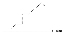
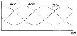
この補正にも対応する、一般的な電圧指令値(パルス幅)の補正例を図38に示す。図38において、横軸は時間を表し、220u、220v及び220wは、U相、V相及びW相の電圧レベルを表している。各相の電圧レベルは各相に対する電圧指令値(パルス幅)に従うため、両者は等価と考えることができる。図38に示す如く、電圧の「最大相と中間相」及び「最小相と中間相」が所定間隔以下に接近しないように、各相の電圧指令値(パルス幅)が補正される。これにより、2相分の電流が検出できないほど各相電圧が接近することがなくなり、安定的に2相分の電流を検出することが可能となる。 A correction example of a general voltage command value (pulse width) corresponding to this correction is shown in FIG. In FIG. 38, the horizontal axis represents time, and 220u, 220v, and 220w represent voltage levels of the U phase, the V phase, and the W phase. Since the voltage level of each phase follows the voltage command value (pulse width) for each phase, both can be considered equivalent. As shown in FIG. 38, the voltage command value (pulse width) of each phase is corrected so that the “maximum phase and intermediate phase” and “minimum phase and intermediate phase” of the voltage do not approach a predetermined interval or less. As a result, the voltages of the phases do not approach so much that the current for two phases cannot be detected, and the current for two phases can be detected stably.
しかしながら、特許文献3に記載の手法では、3相分の電圧指令値(パルス幅)の関係から補正量を決定する必要があり、特に、印加電圧が低い時には3相全てに対して補正が必要となる場合が生じて補正処理が煩雑となる。
However, in the method described in
尚、下記特許文献1には、2相分の電流が検出できなくなることに対する対策手法は記載されていない。また、下記非特許文献1には、系統連系用の三相式インバータに対する制御技術が開示されている。
Note that
上述の如く、1シャント電流検出方式を採用した際、図38に示すような補正は有効ではあるが、同時に、より簡素な処理にて、モータ電流の検出可能状態を維持するための所望の補正を実現する技術が切望されている。また、モータ制御に関わる従来技術について説明したが、その従来技術が抱える問題と同様の問題が、系統連系システムなどに対しても生じうる。 As described above, when the one-shunt current detection method is adopted, the correction as shown in FIG. 38 is effective, but at the same time, a desired correction for maintaining the motor current detectable state by a simpler process. The technology to achieve this is eagerly desired. Moreover, although the prior art regarding motor control was demonstrated, the problem similar to the problem which the prior art has may arise with respect to a grid connection system etc.
そこで本発明は、1シャント電流検出方式を採用した場合において、簡素な処理にて、モータ電流の検出可能状態を維持するための所望の補正を実現可能とするモータ制御装置及びモータ駆動システムを提供することを目的とする。また本発明は、1シャント電流検出方式に対応する電流検出方式を採用し、インバータ出力電流の検出可能状態を維持するための所望の補正を実現可能とする電流検出ユニット、インバータ制御装置及び系統連系装置を提供することを目的とする。 Accordingly, the present invention provides a motor control device and a motor drive system capable of realizing a desired correction for maintaining a motor current detectable state by a simple process when a single shunt current detection method is employed. The purpose is to do. In addition, the present invention adopts a current detection method corresponding to the one shunt current detection method, and realizes a desired correction for maintaining a detectable state of the inverter output current, an inverter control device, and a system connection. An object is to provide a system device.
上記目的を達成するために本発明に係るモータ制御装置は、三相式のモータを駆動するインバータと直流電源との間に流れる電流を検出電流として検出する電流検出手段を備え、検出された前記検出電流から前記モータに流れるモータ電流を検出し、該モータ電流に基づいて前記インバータを介して前記モータを制御するモータ制御装置において、前記モータ電流に基づいて前記モータへの印加電圧が追従すべき電圧のベクトルを表す電圧指令ベクトルを作成する電圧指令ベクトル作成手段と、作成された前記電圧指令ベクトルを補正する電圧指令ベクトル補正手段と、を備え、補正後の前記電圧指令ベクトルに従って前記モータを制御することを特徴とする。 In order to achieve the above object, a motor control device according to the present invention includes current detection means for detecting, as a detection current, a current flowing between an inverter that drives a three-phase motor and a DC power source, In a motor control device that detects a motor current flowing through the motor from a detected current and controls the motor via the inverter based on the motor current, an applied voltage to the motor should follow the motor current A voltage command vector creating means for creating a voltage command vector representing a voltage vector; and a voltage command vector correcting means for correcting the created voltage command vector. The motor is controlled according to the corrected voltage command vector. It is characterized by doing.
例えば、前記電圧指令ベクトルは、回転座標上の電圧指令ベクトルであり、前記電圧指令ベクトル補正手段は、その回転座標上の電圧指令ベクトルを三相の固定座標上の三相電圧指令値に変換する過程において、前記回転座標上の電圧指令ベクトルを補正し、当該モータ制御装置は、補正後の前記電圧指令ベクトルに対応する前記三相電圧指令を前記インバータに供給することにより、前記モータを制御する。 For example, the voltage command vector is a voltage command vector on a rotation coordinate, and the voltage command vector correction means converts the voltage command vector on the rotation coordinate into a three-phase voltage command value on a three-phase fixed coordinate. In the process, the voltage command vector on the rotation coordinate is corrected, and the motor control device controls the motor by supplying the inverter with the three-phase voltage command corresponding to the corrected voltage command vector. .
より具体的には例えば、前記電圧指令ベクトルは、所定の固定軸を基準とした前記電圧指令ベクトルの位相に応じて電気角60度ごとにステップ的に回転するab座標上の二相の電圧指令ベクトルである。 More specifically, for example, the voltage command vector is a two-phase voltage command on the ab coordinate that rotates stepwise every electrical angle 60 degrees in accordance with the phase of the voltage command vector with a predetermined fixed axis as a reference. Is a vector.
これにより、電圧指令ベクトルの座標軸成分を補正するという簡素な処理によって、所望の補正を実現可能となる。 Thereby, a desired correction can be realized by a simple process of correcting the coordinate axis component of the voltage command vector.
つまり例えば、前記電圧指令ベクトル補正手段は、前記ab座標上の二相の電圧指令ベクトルを形成する座標軸成分の大きさに基づいて補正の要否を判断し、補正が必要な場合、前記座標軸成分を補正することによって、前記電圧指令ベクトルを補正する。 That is, for example, the voltage command vector correction means determines whether or not correction is necessary based on the size of the coordinate axis component that forms the two-phase voltage command vector on the ab coordinate. The voltage command vector is corrected by correcting.
また例えば、当該モータ制御装置は、作成された前記電圧指令ベクトルに基づいて前記検出電流として流れる電流の相を判断し、その判断結果に従って前記モータ電流を検出する。 Further, for example, the motor control device determines the phase of the current flowing as the detection current based on the generated voltage command vector, and detects the motor current according to the determination result.
電圧指令ベクトルに基づく上記の判断の手法として、より具体的には以下のような手法が考えられる。例えば、所定の固定軸を基準とした前記電圧指令ベクトルの位相に基づいて前記検出電流として流れる電流の相を判断する。 More specifically, the following method can be considered as a method of the above determination based on the voltage command vector. For example, the phase of the current flowing as the detection current is determined based on the phase of the voltage command vector with a predetermined fixed axis as a reference.
これに代えて例えば、前記ab座標における前記電圧指令ベクトルの座標軸成分と、前記ab座標の座標軸と所定の固定軸との位相差に応じた変数と、に基づいて前記検出電流として流れる電流の相を判断する。 Instead of this, for example, the phase of the current flowing as the detection current based on the coordinate axis component of the voltage command vector in the ab coordinate and a variable according to the phase difference between the coordinate axis of the ab coordinate and a predetermined fixed axis Judging.
そして例えば、当該モータ制御装置は、補正後の前記電圧指令ベクトルから三相電圧指令値を作成する三相電圧指令値作成手段を更に備え、前記判断結果と前記三相電圧指令値に基づいて前記検出電流を検出するタイミングを決定し、そのタイミングにて検出された前記検出電流から前記モータ電流を検出し、前記三相電圧指令値を前記インバータに供給することにより、前記モータを制御する。 And, for example, the motor control device further includes a three-phase voltage command value creating means for creating a three-phase voltage command value from the corrected voltage command vector, and based on the determination result and the three-phase voltage command value, The timing for detecting the detected current is determined, the motor current is detected from the detected current detected at that timing, and the motor is controlled by supplying the three-phase voltage command value to the inverter.
また例えば、作成された前記電圧指令ベクトルの大きさに基づいて前記検出電流を検出するタイミングを決定し、そのタイミングにて検出された前記検出電流から前記モータ電流を検出するようにしてもよい。 Further, for example, a timing for detecting the detected current may be determined based on the magnitude of the generated voltage command vector, and the motor current may be detected from the detected current detected at that timing.
また例えば、前記ab座標における前記電圧指令ベクトルの座標軸成分に基づいて前記検出電流を検出するタイミングを決定し、そのタイミングにて検出された前記検出電流から前記モータ電流を検出するようにしてもよい。 Further, for example, a timing for detecting the detection current may be determined based on a coordinate axis component of the voltage command vector in the ab coordinate, and the motor current may be detected from the detection current detected at the timing. .
また、上記目的を実現するために本発明に係るモータ駆動システムは、三相式のモータと、前記モータを駆動するインバータと、前記インバータを制御することにより前記モータを制御する上記の何れかに記載のモータ制御装置と、を備えたことを特徴とする。 In order to achieve the above object, a motor drive system according to the present invention includes a three-phase motor, an inverter that drives the motor, and any of the above that controls the motor by controlling the inverter. And a motor control device as described above.
また、上記目的を実現するために本発明に係る電流検出ユニットは、三相式のインバータと直流電源との間に流れる電流を検出電流として検出する電流検出手段を備え、検出された前記検出電流から前記インバータの三相電流を検出する電流検出ユニットにおいて、 前記インバータの三相電圧が追従すべき電圧のベクトルを表す電圧指令ベクトルを作成する電圧指令ベクトル作成手段と、作成された前記電圧指令ベクトルを補正する電圧指令ベクトル補正手段と、を備え、補正後の前記電圧指令ベクトルに従って前記インバータは制御されることを特徴とする。 In order to achieve the above object, a current detection unit according to the present invention includes current detection means for detecting a current flowing between a three-phase inverter and a DC power supply as a detection current, and the detected current detected In the current detection unit for detecting the three-phase current of the inverter from the voltage command vector creating means for creating a voltage command vector representing the vector of the voltage that the three-phase voltage of the inverter should follow, and the created voltage command vector Voltage command vector correction means for correcting the voltage, and the inverter is controlled in accordance with the corrected voltage command vector.
例えば、前記電流検出ユニットにおいて、前記電圧指令ベクトルは、回転座標上の電圧指令ベクトルであり、前記電圧指令ベクトル補正手段は、その回転座標上の電圧指令ベクトルを三相の固定座標上の三相電圧指令値に変換する過程において、前記回転座標上の電圧指令ベクトルを補正し、補正後の前記電圧指令ベクトルに対応する前記三相電圧指令値が前記インバータに供給されることによって、前記インバータは制御される。 For example, in the current detection unit, the voltage command vector is a voltage command vector on a rotation coordinate, and the voltage command vector correction means converts the voltage command vector on the rotation coordinate to a three-phase fixed coordinate on three phases. In the process of converting to a voltage command value, the voltage command vector on the rotation coordinate is corrected, and the inverter is supplied with the three-phase voltage command value corresponding to the corrected voltage command vector. Be controlled.
より具体的には例えば、前記電流検出ユニットにおいて、前記電圧指令ベクトルは、所定の固定軸を基準とした前記電圧指令ベクトルの位相に応じて電気角60度ごとにステップ的に回転するab座標上の二相の電圧指令ベクトルである。 More specifically, for example, in the current detection unit, the voltage command vector is an ab coordinate that rotates stepwise at every electrical angle of 60 degrees according to the phase of the voltage command vector with respect to a predetermined fixed axis. Is a two-phase voltage command vector.
これにより、電圧指令ベクトルの座標軸成分を補正するという簡素な処理によって、所望の補正を実現可能となる。 Thereby, a desired correction can be realized by a simple process of correcting the coordinate axis component of the voltage command vector.
つまり例えば、前記電流検出ユニットにおいて、前記電圧指令ベクトル補正手段は、前記ab座標上の二相の電圧指令ベクトルを形成する座標軸成分の大きさに基づいて補正の要否を判断し、補正が必要な場合、前記座標軸成分を補正することによって、前記電圧指令ベクトルを補正する。 That is, for example, in the current detection unit, the voltage command vector correction means determines whether or not correction is necessary based on the size of the coordinate axis component forming the two-phase voltage command vector on the ab coordinate, and correction is necessary. In this case, the voltage command vector is corrected by correcting the coordinate axis component.
また、本発明に係るインバータ制御装置は、上記の電流検出ユニットを備え、検出した前記三相電流に基づいて前記インバータを制御するインバータ制御装置であって、前記電圧指令ベクトル作成手段は、前記三相電流に基づいて前記電圧指令ベクトルを作成することを特徴とする。 An inverter control device according to the present invention is an inverter control device that includes the above-described current detection unit and controls the inverter based on the detected three-phase current, wherein the voltage command vector creating means includes the three The voltage command vector is generated based on a phase current.
そして例えば、前記インバータ制御装置は、前記インバータの出力電圧の位相を基準として前記三相電流を有効電流と無効電流に変換する電流変換手段を更に備え、前記電圧指令ベクトル作成手段は、前記有効電流及び前記無効電流に基づいて前記電圧指令ベクトルを作成する。 For example, the inverter control device further includes current conversion means for converting the three-phase current into effective current and reactive current with reference to the phase of the output voltage of the inverter, and the voltage command vector creation means includes the effective current The voltage command vector is generated based on the reactive current.
また、本発明に係る系統連系装置は、上記のインバータ制御装置及びインバータを備え、前記直流電源からの直流電圧を前記インバータによって三相の交流電圧に変換し、外部の三相交流電力系統に連系しつつ前記交流電圧に基づく交流電力を負荷に供給することを特徴とする。 Further, a grid interconnection device according to the present invention includes the inverter control device and the inverter described above, converts a DC voltage from the DC power source into a three-phase AC voltage by the inverter, and converts it into an external three-phase AC power system. AC power based on the AC voltage is supplied to a load while being connected.
本発明によれば、1シャント電流検出方式を採用した場合において、簡素な処理にて所望の補正が実現可能となる。 According to the present invention, when the single shunt current detection method is adopted, desired correction can be realized by a simple process.
以下、本発明の実施の形態につき、図面を参照して具体的に説明する。参照される各図において、同一の部分には同一の符号を付し、同一の部分に関する重複する説明を原則として省略する。 Hereinafter, embodiments of the present invention will be specifically described with reference to the drawings. In each of the drawings to be referred to, the same part is denoted by the same reference numeral, and redundant description regarding the same part is omitted in principle.
<<第1実施形態>>
まず、本発明の第1実施形態について説明する。後に、第1実施形態における第1〜第5実施例を説明するが、まず、それらの各実施例に共通する事項及び各実施例にて参照される事項について説明する。図1は、第1実施形態に係るモータ駆動システムのブロック構成図である。
<< First Embodiment >>
First, a first embodiment of the present invention will be described. Later, first to fifth examples of the first embodiment will be described. First, matters common to the examples and items to be referred to in the examples will be described. FIG. 1 is a block diagram of a motor drive system according to the first embodiment.
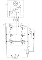
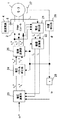
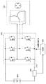
図1のモータ駆動システムは、三相永久磁石同期モータ1(以下、単に「モータ1」と記す)と、PWM(Pulse Width Modulation)インバータ2(以下、単に「インバータ2」という)と、制御部3と、直流電源4と、電流センサ5と、を備える。直流電源4は、負出力端子4bを低電圧側として、正出力端子4aと負出力端子4bとの間に直流電圧を出力する。図1のモータ駆動システムは、1シャント電流検出方式を採用している。
1 includes a three-phase permanent magnet synchronous motor 1 (hereinafter simply referred to as “
モータ1は、永久磁石が設けられた回転子6と、U相、V相及びW相の電機子巻線7u、7v及び7wが設けられた固定子7と、を備えている。電機子巻線7u、7v及び7wは、中性点14を中心にY結線されている。電機子巻線7u、7v及び7wにおいて、中性点14の反対側の非結線端は、夫々、端子12u、12v及び12wに接続されている。
The
インバータ2は、U相用のハーフブリッジ回路、V相用のハーフブリッジ回路及びW相用のハーフブリッジ回路を備える。各ハーフブリッジ回路は、一対のスイッチング素子を有する。各ハーフブリッジ回路において、一対のスイッチング素子は、直流電源4の正出力端子4aと負出力端子4bとの間に直列接続され、各ハーフブリッジ回路に直流電源4からの直流電圧が印加される。
The
U相用のハーフブリッジ回路は、高電圧側のスイッチング素子8u(以下、上アーム8uとも呼ぶ)及び低電圧側のスイッチング素子9u(以下、下アーム9uとも呼ぶ)から成る。V相用のハーフブリッジ回路は、高電圧側のスイッチング素子8v(以下、上アーム8vとも呼ぶ)及び低電圧側のスイッチング素子9v(以下、下アーム9vとも呼ぶ)から成る。W相用のハーフブリッジ回路は、高電圧側のスイッチング素子8w(以下、上アーム8wとも呼ぶ)及び低電圧側のスイッチング素子9w(以下、下アーム9wとも呼ぶ)から成る。また、スイッチング素子8u、8v、8w、9u、9v及び9wには、夫々、並列に、直流電源4の低電圧側から高電圧側に向かう方向を順方向としてダイオード10u、10v、10w、11u、11v及び11wが接続されている。各ダイオードは、フリーホイールダイオードとして機能する。
The U-phase half-bridge circuit includes a high-voltage
直列接続された上アーム8uと下アーム9uの接続点、直列接続された上アーム8vと下アーム9vの接続点、直列接続された上アーム8wと下アーム9wの接続点は、夫々、端子12u、12v及び12wに接続される。尚、図1では、各スイッチング素子として電界効果トランジスタが示されているが、それらをIGBT(絶縁ゲートバイポーラトランジスタ)などに置き換えることもできる。
The connection point between the
インバータ2は、制御部3から与えられた三相電圧指令値に基づいて各相に対するPWM信号(パルス幅変調信号)を生成し、該PWM信号をインバータ2内の各スイッチング素子の制御端子(ベース又はゲート)に与えることで、各スイッチング素子をスイッチング動作させる。制御部3からインバータ2に供給される三相電圧指令値は、U相電圧指令値vu *、V相電圧指令値vv *及びW相電圧指令値vw *から構成され、vu *、vv *及びvw *によって、夫々、U相電圧vu、V相電圧vv及びW相電圧vwの電圧レベル(電圧値)が表される。そして、インバータ2は、vu *、vv *及びvw *に基づいて、各スイッチング素子のオン(導通)又はオフ(非導通)を制御する。
The
同一の相の上アームと下アームが同時にオンとなるのを防ぐためのデッドタイムを無視すると、各ハーフブリッジ回路において、上アームがオンである時は下アームはオフであり、上アームがオフである時は下アームはオンである。以下の説明は、上記デッドタイムを無視して行うものとする。 Neglecting the dead time to prevent the upper and lower arms of the same phase from turning on at the same time, in each half-bridge circuit, when the upper arm is on, the lower arm is off and the upper arm is off When, the lower arm is on. In the following description, the dead time is ignored.
インバータ2に印加されている直流電源4からの直流電圧は、インバータ2内の各スイッチング素子のスイッチング動作によって、例えば、PWM変調(パルス幅変調)された三相交流電圧に変換される。該三相交流電圧がモータ1に印加されることによって、各電機子巻線(7u、7v及び7w)に、三相交流電圧に応じた電流が流れてモータ1が駆動される。
The DC voltage from the
電流センサ5は、インバータ2の母線13に流れる電流(以下、「母線電流」という)を検出する。母線電流は直流成分を有するため、それを直流電流と解釈することもできる。インバータ2において、下アーム9u、9v及び9wの低電圧側は共通結線されて直流電源4の負出力端子4bに接続される。下アーム9u、9v及び9wの低電圧側が共通結線される配線が母線13であり、電流センサ5は、母線13に直列に介在している。電流センサ5は、検出した母線電流(検出電流)の電流値を表す信号を制御部3に伝達する。制御部3は、電流センサ5の出力信号等を参照しつつ上記三相電圧指令値を生成及び出力する。尚、電流センサ5は、例えば、シャント抵抗又はカレントトランス等である。また、下アーム9u、9v及び9wの低電圧側と負出力端子4bとを接続する配線(母線13)にではなく、上アーム8u、8v及び8wの高電圧側と正出力端子4aとを接続する配線に電流センサ5を設けるようにしてもよい。
ここで、図2〜図6を用いて、母線電流と各相の電機子巻線に流れる相電流との関係等について説明する。電機子巻線7u、7v及び7wに流れる電流を、夫々、U相電流、V相電流及びW相電流と呼び、それらの夫々を(或いはそれらを総称して)相電流と呼ぶ(図1参照)。また、相電流において、端子12u、12v又は12wから中性点14に流れ込む方向の電流の極性を正とし、中性点14から流れ出す方向の電流の極性を負とする。
Here, the relationship between the bus current and the phase current flowing through the armature winding of each phase will be described with reference to FIGS. The currents that flow through the
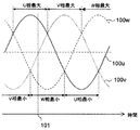
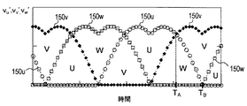
図2は、モータ1に印加される三相交流電圧の典型的な例を示す。図2において、100u、100v及び100wは、夫々、モータ1に印加されるべきU相電圧、V相電圧及びW相電圧の波形を表す。U相電圧、V相電圧及びW相電圧の夫々を(或いはそれらを総称して)相電圧と呼ぶ。モータ1に正弦波状の電流を流す場合、インバータ2の出力電圧は正弦波状とされる。尚、図2の各相電圧は理想的な正弦波となっているが、本実施形態において、実際には該正弦波に歪みが加えられる(詳細は後述)。
FIG. 2 shows a typical example of a three-phase AC voltage applied to the
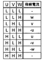
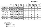
図2に示す如く、U相電圧、V相電圧及びW相電圧の間の電圧レベルの高低関係は、時間の経過と共に変化していく。この高低関係は三相電圧指令値によって定まり、インバータ2は三相電圧指令値に従って各相に対する通電パターンを決定する。図3に、この通電パターンを表として示す。図3の左側から第1列目〜第3列目に通電パターンを表す。第4列目については後述する。
As shown in FIG. 2, the level relationship of the voltage level among the U-phase voltage, the V-phase voltage, and the W-phase voltage changes with time. This level relationship is determined by the three-phase voltage command value, and the
通電パターンには、
U、V及びW相の下アームが全てオンの通電パターン「LLL」と、
W相の上アームがオン且つU及びV相の下アームがオンの通電パターン「LLH」と、
V相の上アームがオン且つU及びW相の下アームがオンの通電パターン「LHL」と、
V及びW相の上アームがオン且つU相の下アームがオンの通電パターン「LHH」と、
U相の上アームがオン且つV及びW相の下アームがオンの通電パターン「HLL」と、
U及びW相の上アームがオン且つV相の下アームがオンの通電パターン「HLH」と、
U及びV相の上アームがオン且つW相の下アームがオンの通電パターン「HHL」と、
U、V及びW相の上アームが全てオンの通電パターン「HHH」と、
がある(上アーム及び下アームの符号(8u等)を省略して記載)。
In the energization pattern,
The energization pattern “LLL” in which the lower arms of the U, V, and W phases are all on,
An energization pattern “LLH” in which the upper arm of the W phase is on and the lower arm of the U and V phases is on,
An energization pattern “LHL” in which the upper arm of the V phase is on and the lower arm of the U and W phases is on,
An energization pattern “LHH” in which the upper arm of the V and W phases is on and the lower arm of the U phase is on,
An energization pattern “HLL” in which the upper arm of the U phase is on and the lower arm of the V and W phases is on,
An energization pattern “HLH” in which the upper arm of the U and W phases is on and the lower arm of the V phase is on,
An energization pattern “HHL” in which the upper arm of the U and V phases is on and the lower arm of the W phase is on,
The energization pattern “HHH” in which the upper arms of the U, V, and W phases are all on,
(The upper arm and lower arm symbols (8u, etc.) are omitted).
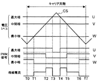
図4に、3相変調を行う場合における、各相電圧の電圧レベルとキャリア信号との関係、並びに、その関係に応じたPWM信号及び母線電流の波形を示す。各相電圧の電圧レベルの高低関係は様々に変化するが、説明の具体化のため、図4は、図2に示す或るタイミング101に着目している。即ち、図4は、U相電圧の電圧レベルが最大であって且つW相電圧の電圧レベルが最小である場合を示している。電圧レベルが最大の相を「最大相」、電圧レベルが最小の相を「最小相」、電圧レベルが最大でも最小でもない相を「中間相」と呼ぶ。図4に示す状態では、最大相、中間相及び最小相は、夫々、U相、V相及びW相となっている。図4において、符号CSは各相電圧の電圧レベルと比較されるキャリア信号を表す。キャリア信号は周期的な三角波信号となっており、その信号の周期をキャリア周期という。尚、キャリア周期は、図2に示す三相交流電圧の周期よりも遥かに短いため、仮に図4に示すキャリア信号の三角波を図2上で表すと、その三角波は1本の線となって見える。
FIG. 4 shows the relationship between the voltage level of each phase voltage and the carrier signal in the case of performing three-phase modulation, and the waveforms of the PWM signal and bus current corresponding to the relationship. Although the level relationship of the voltage level of each phase voltage varies in various ways, FIG. 4 focuses on a
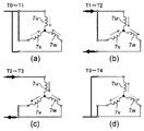
図5(a)〜(d)を更に参照して相電流と母線電流との関係について説明する。図5は、図4の各タイミングにおける、電機子巻線周辺の等価回路である。 The relationship between the phase current and the bus current will be described with further reference to FIGS. FIG. 5 is an equivalent circuit around the armature winding at each timing of FIG.
各キャリア周期の開始タイミング、即ちキャリア信号が最低レベルにあるタイミングをT0と呼ぶ。タイミングT0において、各相の上アーム(8u、8v及び8w)はオンとされる。この場合、図5(a)に示す如く、短絡回路が形成されて直流電源4への電流の出入りがない状態となるため、母線電流はゼロとなる。
The start timing of each carrier period, that is, the timing at which the carrier signal is at the lowest level is called T0. At the timing T0, the upper arms (8u, 8v and 8w) of the respective phases are turned on. In this case, as shown in FIG. 5 (a), a short circuit is formed and no current flows in or out of the
インバータ2は、vu *、vv *及びvw *を参照して各相電圧の電圧レベルとキャリア信号を比較する。そして、キャリア信号のレベル(電圧レベル)の上昇過程において、最小相の電圧レベルがキャリア信号と交差するタイミングT1に至ると、最小相の下アームがオンとされ、図5(b)に示す如く、最小相の電流が母線電流として流れる。図4に示す例の場合、タイミングT1から後述のタイミングT2に至るまでの間は、W相の下アーム9wがオンとなるため、W相電流(極性は負)が母線電流として流れる。
The
更にキャリア信号のレベルが上昇して中間相の電圧レベルがキャリア信号と交差するタイミングT2に至ると、最大相の上アームがオン且つ中間相及び最小相の下アームがオンとなって、図5(c)に示す如く、最大相の電流が母線電流として流れる。図4に示す例の場合、タイミングT2から後述のタイミングT3に至るまでの間は、U相の上アーム8uがオン且つV相及びW相の下アーム9v及び9wがオンとなるため、U相電流(極性は正)が母線電流として流れる。
Further, when the level of the carrier signal rises and reaches a timing T2 at which the voltage level of the intermediate phase intersects with the carrier signal, the upper arm of the maximum phase is turned on and the lower arm of the intermediate phase and the minimum phase are turned on. As shown in (c), the maximum phase current flows as the bus current. In the example shown in FIG. 4, the U-phase
更にキャリア信号のレベルが上昇して最大相の電圧レベルがキャリア信号と交差するタイミングT3に至ると、全ての相の下アームがオンとなって、図5(d)に示す如く、短絡回路が形成されて直流電源4への電流の出入りがない状態となるため、母線電流はゼロとなる。
When the carrier signal level further rises and the timing T3 at which the maximum phase voltage level intersects with the carrier signal is reached, the lower arms of all phases are turned on, and as shown in FIG. Since it is formed and no current flows into and out of the
タイミングT3と後述するタイミングT4の中間タイミングにおいて、キャリア信号が最大レベルに達した後、キャリア信号のレベルは下降していく。キャリア信号のレベルの下降過程では、図5(d)、(c)、(b)及び(a)に示す状態が、この順番で訪れる。即ち、キャリア信号のレベルの下降過程において、最大相の電圧レベルがキャリア信号と交差するタイミングをT4、中間相の電圧レベルがキャリア信号と交差するタイミングをT5、最小相の電圧レベルがキャリア信号と交差するタイミングをT6、次のキャリア周期の開始タイミングをT7とすると、タイミングT4−T5間、タイミングT5−T6間、タイミングT6−T7間は、夫々、タイミングT2−T3間、タイミングT1−T2間、タイミングT0−T1間と同じ通電パターンとなる。 After the carrier signal reaches the maximum level at an intermediate timing between timing T3 and timing T4 described later, the level of the carrier signal decreases. In the process of decreasing the level of the carrier signal, the states shown in FIGS. 5D, 5C, 5B, and 5A are visited in this order. That is, in the lowering process of the carrier signal level, the timing when the maximum phase voltage level intersects the carrier signal is T4, the timing when the intermediate phase voltage level intersects the carrier signal is T5, and the minimum phase voltage level is the carrier signal. Assuming that the intersection timing is T6 and the next carrier cycle start timing is T7, the timing T4-T5, the timing T5-T6, and the timing T6-T7 are between the timing T2-T3 and the timing T1-T2, respectively. The same energization pattern as that between the timings T0 and T1 is obtained.
従って例えば、タイミングT1−T2間或いはT5−T6間で母線電流を検出すれば、母線電流から最小相の電流を検出することができ、タイミングT2−T3間或いはT4−T5間で母線電流を検出すれば、母線電流から最大相の電流を検出することができる。そして、中間相の電流は、三相電流の総和が0になることを利用して計算で得ることができる。図3の表の第4列目には、各通電パターンにおいて母線電流として流れる電流の相を、電流極性付きで示している。例えば、図3の表の8行目に対応する通電パターン「HHL」においては、母線電流としてW相電流(極性は負)が流れる。 Therefore, for example, if the bus current is detected between timings T1 and T2 or between T5 and T6, the minimum phase current can be detected from the bus current, and the bus current is detected between timings T2 and T3 or between T4 and T5. Then, the maximum phase current can be detected from the bus current. The intermediate phase current can be obtained by calculation using the fact that the sum of the three phase currents becomes zero. In the fourth column of the table of FIG. 3, the phase of the current that flows as the bus current in each energization pattern is shown with a current polarity. For example, in the energization pattern “HHL” corresponding to the eighth row in the table of FIG. 3, a W-phase current (negative polarity) flows as the bus current.
尚、キャリア周期からタイミングT1とT6との間の期間を除いた期間は最小相に対するPWM信号のパルス幅を表し、キャリア周期からタイミングT2とT5との間の期間を除いた期間は中間相に対するPWM信号のパルス幅を表し、キャリア周期からタイミングT3とT4との間の期間を除いた期間は最大相に対するPWM信号のパルス幅を表す。 The period excluding the period between the timings T1 and T6 from the carrier period represents the pulse width of the PWM signal for the minimum phase, and the period excluding the period between the timings T2 and T5 from the carrier period is for the intermediate phase. This represents the pulse width of the PWM signal, and the period excluding the period between timings T3 and T4 from the carrier period represents the pulse width of the PWM signal for the maximum phase.
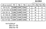
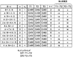
U相が最大相且つW相が最小相の場合を例に挙げたが、最大相、中間相及び最小相の組み合わせは、6通りある。図6に、この組み合わせを表として示す。U相電圧、V相電圧及びW相電圧を、夫々、vu、vv及びvwで表した場合において、
vu>vv>vw、が成立する状態を第1モード、
vv>vu>vw、が成立する状態を第2モード、
vv>vw>vu、が成立する状態を第3モード、
vw>vv>vu、が成立する状態を第4モード、
vw>vu>vv、が成立する状態を第5モード、
vu>vw>vv、が成立する状態を第6モード、
と呼ぶ。図4及び図5に示した例は、第1モードに対応している。また、図6には、各モードにおいて検出される電流の相も示されている。
The case where the U phase is the maximum phase and the W phase is the minimum phase has been described as an example, but there are six combinations of the maximum phase, the intermediate phase, and the minimum phase. FIG. 6 shows this combination as a table. When the U-phase voltage, V-phase voltage, and W-phase voltage are represented by v u , v v, and v w , respectively,
The state in which v u > v v > v w is satisfied is the first mode,
The state in which v v > v u > v w is established is the second mode,
The state in which v v > v w > v u is established is the third mode,
The state in which v w > v v > v u is established is the fourth mode,
The state in which v w > v u > v v is established is the fifth mode,
The state in which v u > v w > v v is established is the sixth mode,
Call it. The examples shown in FIGS. 4 and 5 correspond to the first mode. FIG. 6 also shows the phase of current detected in each mode.
U相電圧指令値vu *、V相電圧指令値vv *及びW相電圧指令値vw *は、具体的には、夫々、カウンタの設定値CntU、CntV及びCntWとして表される。相電圧が高いほど、大きな設定値が与えられる。例えば、第1モードにおいては、CntU>CntV>CntW、が成立する。 Specifically, the U-phase voltage command value v u * , the V-phase voltage command value v v *, and the W-phase voltage command value v w * are expressed as counter setting values CntU, CntV, and CntW, respectively. The higher the phase voltage, the greater the set value. For example, in the first mode, CntU>CntV> CntW is satisfied.
制御部3に設けられたカウンタ(不図示)は、キャリア周期ごとに、タイミングT0を基準としてカウント値を0からアップカウントする。そして、そのカウント値がCntWに達した時点でW相の上アーム8wがオンの状態から下アーム9wがオンの状態に切り替えられ、そのカウント値がCntVに達した時点でV相の上アーム8vがオンの状態から下アーム9vがオンの状態に切り替えられ、そのカウント値がCntUに達した時点でU相の上アーム8uがオンの状態から下アーム9uがオンの状態に切り替えられる。キャリア信号が最大レベルに達した後は、カウント値はダウンカウントされ、逆の切り替え動作が行われる。
A counter (not shown) provided in the
従って、第1モードにおいては、上記のカウンタ値がCntWに達した時点がタイミングT1に対応し、CntVに達した時点がタイミングT2に対応し、CntUに達した時点がタイミングT3に対応することになる。このため、第1モードにおいては、カウンタ値がアップカウントされている状態で、カウンタ値がCntWより大きく且つCntVより小さいタイミングに電流センサ5の出力信号をサンプリングすることにより母線電流として流れるW相電流(極性は負)を検出することができ、カウンタ値がCntVより大きく且つCntUより小さいタイミングに電流センサ5の出力信号をサンプリングすることにより、母線電流として流れるU相電流(極性は正)を検出することができる。
Therefore, in the first mode, the time when the counter value reaches CntW corresponds to timing T1, the time when CntV is reached corresponds to timing T2, and the time when CntU reaches CntU corresponds to timing T3. Become. Therefore, in the first mode, the W-phase current that flows as the bus current by sampling the output signal of the
同様に考えて、図6に示す如く、第2モードにおいては、上記のカウンタ値がCntWに達した時点がタイミングT1に対応し、CntUに達した時点がタイミングT2に対応し、CntVに達した時点がタイミングT3に対応することになる。このため、第2モードにおいては、カウンタ値がアップカウントされている状態で、カウンタ値がCntWより大きく且つCntUより小さいタイミングの母線電流からW相電流(極性は負)を検出することができ、カウンタ値がCntUより大きく且つCntVより小さいタイミングの母線電流からV相電流(極性は正)を検出することができる。第3〜第6モードについても同様である。 Similarly, as shown in FIG. 6, in the second mode, the time when the counter value reaches CntW corresponds to the timing T1, and the time when the counter value reaches CntU corresponds to the timing T2 and reaches CntV. The time point corresponds to the timing T3. For this reason, in the second mode, the W-phase current (polarity is negative) can be detected from the bus current at the timing when the counter value is larger than CntW and smaller than CntU in a state where the counter value is up-counted. The V-phase current (polarity is positive) can be detected from the bus current at the timing when the counter value is larger than CntU and smaller than CntV. The same applies to the third to sixth modes.
また、タイミングT1−T2間の、最小相の相電流を検出するサンプリングタイミング(例えば、タイミングT1とT2の中間タイミング)をST1にて表し、タイミングT2−T3間の、最大相の相電流を検出するサンプリングタイミング(例えば、タイミングT2とT3の中間タイミング)をST2にて表す。 In addition, the sampling timing for detecting the phase current of the minimum phase between timings T1 and T2 (for example, an intermediate timing between timings T1 and T2) is represented by ST1, and the phase current of the maximum phase between timings T2 and T3 is detected. A sampling timing to be performed (for example, an intermediate timing between timings T2 and T3) is represented by ST2.
尚、三相電圧指令値(vu *、vv *及びvw *)としてのカウンタの設定値CntU、CnuV及びCntWによって、各相に対するPWM信号のパルス幅(及びデューティ)は特定される。 The pulse width (and duty) of the PWM signal for each phase is specified by the counter setting values CntU, CnuV, and CntW as the three-phase voltage command values (v u * , v v *, and v w * ).
上述の原理に基づき母線電流から各相電流を検出することができるのであるが、図4を参照して理解されるように、例えば最大相と中間相の電圧レベルが接近するとタイミングT2−T3間及びT4−T5間の時間長さが短くなる。母線電流は図1の電流センサ5からのアナログ出力信号をデジタル信号に変換することによって検出されるが、この時間長さが極端に短いと、必要なA/D変換時間やリンギング(スイッチングに由来して生じる電流脈動)の収束時間を確保できなくなって、最大相の相電流を検出できなくなる。同様に、最小相と中間相の電圧レベルが接近すると、最小相の相電流を検出できなくなる。2相分の電流を実測できなければ、3相分の相電流を再現することはできず、モータ1をベクトル制御することはできない。
Each phase current can be detected from the bus current based on the above-described principle. As understood with reference to FIG. 4, for example, when the voltage levels of the maximum phase and the intermediate phase approach each other, the timing T2-T3. And the time length between T4-T5 becomes short. The bus current is detected by converting the analog output signal from the
本実施形態(後述する各実施例)では、このような2相分の電流を実測できなくなると考えられる期間において、モータ1への印加電圧を表す電圧ベクトル(電圧指令ベクトル)を補正して各相電圧間の電圧レベル差を所定値以上に保ち、これによって上記の不具合を解消する。
In the present embodiment (each example to be described later), in a period in which it is considered that currents for two phases cannot be measured, a voltage vector (voltage command vector) representing a voltage applied to the
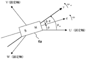
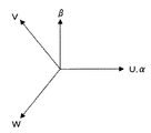
この補正手法の詳細な説明の前に、各種の状態量(状態変数)の説明及び定義等を行う。図7は、モータ1の解析モデル図である。図7には、U相、V相、W相の電機子巻線固定軸(以下、それらを、単に、U相軸、V相軸及びW相軸とも呼ぶ)が示されている。6aは、モータ1の回転子6に設けられた永久磁石である。永久磁石6aが作る磁束と同じ速度で回転する回転座標系において、永久磁石6aが作る磁束の方向をd軸にとる。また、図示していないが、d軸から電気角で90度進んだ位相にq軸をとる。
Prior to detailed description of this correction method, various state quantities (state variables) will be described and defined. FIG. 7 is an analysis model diagram of the
また、モータ1にベクトル制御を行うに際して回転子位置検出用の位置センサを用いない場合は、真のd軸及びq軸が不明であるため、制御上の推定軸が定義される。d軸に対応する制御上の推定軸をγ軸とし、q軸に対応する制御上の推定軸をδ軸とする。δ軸は、γ軸から電気角で90度進んだ軸である(図7において不図示)。通常、ベクトル制御は、γ軸及びδ軸がd軸及びq軸と一致するように実施される。d軸とq軸は、実軸の回転座標系の座標軸であり、それらを座標軸に選んだ座標をdq座標とよぶ。γ軸とδ軸は、制御上の回転座標系(推定回転座標系)の座標軸であり、それらを座標軸に選んだ座標をγδ座標とよぶ。
Further, when the position control for detecting the rotor position is not used when performing vector control on the
d軸(及びq軸)は回転しており、その回転速度(電気角速度)を実モータ速度ωと呼ぶ。γ軸(及びδ軸)も回転しており、その回転速度(電気角速度)を推定モータ速度ωeと呼ぶ。また、ある瞬間の回転しているdq座標において、d軸の位相をU相の電機子巻線固定軸を基準としてθ(実回転子位置θ)により表す。同様に、ある瞬間の回転しているγδ座標において、γ軸の位相をU相の電機子巻線固定軸を基準としてθe(推定回転子位置θe)により表す。そうすると、d軸とγ軸との軸誤差Δθは、Δθ=θ―θeで表される。 The d-axis (and q-axis) is rotating, and the rotation speed (electrical angular speed) is called the actual motor speed ω. The γ-axis (and δ-axis) is also rotating, and the rotation speed (electrical angular speed) is called the estimated motor speed ω e . In addition, in dq coordinates rotating at a certain moment, the phase of the d-axis is represented by θ (actual rotor position θ) with respect to the U-phase armature winding fixed axis. Similarly, in a rotating γδ coordinate at a certain moment, the phase of the γ axis is represented by θ e (estimated rotor position θ e ) with respect to the U-phase armature winding fixed axis. Then, the axis error [Delta] [theta] between the d-axis and the γ-axis is expressed by Δθ = θ-θ e.
また、インバータ2からモータ1に印加される全体のモータ電圧をVaにて表し、インバータ2からモータ1に供給される全体のモータ電流をIaにて表す。そして、
モータ電圧Vaのγ軸成分、δ軸成分、d軸成分及びq軸成分を、それぞれγ軸電圧vγ、δ軸電圧vδ、d軸電圧vd及びq軸電圧vqで表し、
モータ電流Iaのγ軸成分、δ軸成分、d軸成分及びq軸成分を、それぞれγ軸電流iγ、δ軸電流iδ、d軸電流id及びq軸電流iqで表す。
Further, a whole motor voltage that is applied to the
The γ-axis component, δ-axis component, d-axis component, and q-axis component of the motor voltage V a are represented by γ-axis voltage vγ, δ-axis voltage vδ, d-axis voltage v d, and q-axis voltage v q , respectively.
Γ-axis component of the motor current I a, [delta] -axis component, a d-axis component and q-axis components, respectively γ-axis current i?, [Delta] -axis current i?, Expressed in d-axis current i d and the q-axis current i q.
また、後の各実施例でも参照されるが、γ軸電圧vγ、δ軸電圧vδ、d軸電圧vd及びq軸電圧vqに対する指令値(電圧指令値)を、夫々、γ軸電圧指令値vγ*、δ軸電圧指令値vδ*、d軸電圧指令値vd *及びq軸電圧指令値vq *にて表す。vγ*、vδ*、vd *及びvq *は、モータ駆動システム内において算出され、夫々、vγ、vδ、vd及びvqが追従すべき電圧(電圧値)を表す。 Also, as will be referred to in each of the following embodiments, command values (voltage command values) for the γ-axis voltage vγ, δ-axis voltage vδ, d-axis voltage v d, and q-axis voltage v q are respectively expressed as γ-axis voltage command. It is represented by a value vγ * , a δ-axis voltage command value vδ * , a d-axis voltage command value v d *, and a q-axis voltage command value v q * . vγ *, vδ *, v d * and v q * are calculated in the motor driving system, representing respectively, v?, v?, v d and v q voltage should follow the (voltage value).
また更に、γ軸電流iγ、δ軸電流iδ、d軸電流id及びq軸電流iqに対する指令値(電流指令値)を、夫々、γ軸電流指令値iγ*、δ軸電流指令値iδ*、d軸電流指令値id *及びq軸電流指令値iq *にて表す。iγ*、iδ*、id *及びiq *は、モータ駆動システム内において算出され、夫々、iγ、iδ、id及びiqが追従すべき電流(電流値)を表す。 Furthermore, command values (current command values) for the γ-axis current iγ, δ-axis current iδ, d-axis current i d and q-axis current i q are respectively expressed as γ-axis current command value iγ * and δ-axis current command value iδ. * , D-axis current command value i d * and q-axis current command value i q * . i γ * , i δ * , i d * and i q * are calculated in the motor drive system and represent currents (current values) to be followed by i γ, i δ , i d and i q , respectively.
[補正手法について]
以下に、本実施形態の特徴的な機能である、電圧ベクトルの補正手法について説明する。
[About correction method]
The voltage vector correction method, which is a characteristic function of the present embodiment, will be described below.
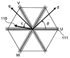
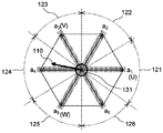
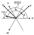
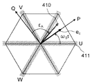
図8に、固定軸であるU相軸、V相軸及びW相軸と、回転軸であるd軸及びq軸と、電圧ベクトルと、の関係を表す空間ベクトル図を示す。符号110が付されたベクトルが、電圧ベクトルである。q軸から見た電圧ベクトル110の位相をεにて表す。U相軸を基準とした電圧ベクトル110の位相は、(θ+ε+π/2)にて表される。
FIG. 8 is a space vector diagram showing the relationship between the U-phase axis, the V-phase axis, and the W-phase axis that are fixed axes, the d-axis and the q-axis that are rotation axes, and the voltage vector. A vector denoted by
電圧ベクトル110は、モータ1に印加される電圧をベクトルとして捉えたものであり、例えばdq座標に着目した場合、電圧ベクトル110のd軸成分及びq軸成分は、それぞれvd及びvqである。実際には、モータ駆動システム内においてd軸電圧指令値vd *及びq軸電圧指令値vq *が算出され、vd *及びvq *によって電圧ベクトル110が表される。このため、電圧ベクトルは、電圧指令ベクトルとも読み替えられる。
The
U相軸近傍、V相軸近傍及びW相軸近傍のハッチングが施されたアスタリスク状の領域111は、2相分の電流が検出できない領域を表している。例えば、V相電圧とW相電圧が近くて2相分の電流が検出できない場合、電圧ベクトル110はU相軸近傍に位置することになり、U相電圧とW相電圧が近くて2相分の電流が検出できない場合、電圧ベクトル110はV相軸近傍に位置することになる。
An asterisk-shaped
このように、2相分の電流が検出不可能な領域111は、U相軸を基準として電気角で60度ごとに存在し、電圧ベクトル110が、その領域111に位置すると2相分の電流が検出できない。従って、電圧ベクトルが領域111内にある場合に、電圧ベクトルが領域111外のベクトルとなるように電圧ベクトルを補正してやればよい。
Thus, the
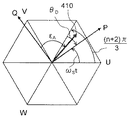
この補正を実行するべく、今、2相分の電流を検出不可能な領域111の特性に着目して、電気角60度ごとにステップ的に回転する座標を考える。この座標を、ab座標と呼ぶ(尚、dq座標やγδ座標は連続的に回転する座標である)。ab座標は、互いに直交するa軸とb軸を座標軸としている。図9に、a軸がとり得る6つの軸を示す。a軸は、電圧ベクトル110の位相(θ+ε+π/2)に応じて、a1軸〜a6軸の何れかとなる。a1軸、a3軸及びa5軸は、それぞれU相軸、V相軸及びW相軸に一致し、a2軸、a4軸及びa6軸は、それぞれa1軸とa3軸の中間軸、a3軸とa5軸の中間軸及びa5軸とa1軸の中間軸である。尚、符号131が付された円については後述する。
In order to execute this correction, attention is now paid to the characteristics of the
電圧ベクトル110が、符号121が付された範囲に位置する場合、即ち、
11π/6≦(θ+ε+π/2)<0、又は、0≦(θ+ε+π/2)<π/6、が成立する場合、a軸はa1軸となり、
電圧ベクトル110が、符号122が付された範囲に位置する場合、即ち、
π/6≦(θ+ε+π/2)<π/2、が成立する場合、a軸はa2軸となり
電圧ベクトル110が、符号123が付された範囲に位置する場合、即ち、
π/2≦(θ+ε+π/2)<5π/6、が成立する場合、a軸はa3軸となり
電圧ベクトル110が、符号124が付された範囲に位置する場合、即ち、
5π/6≦(θ+ε+π/2)<7π/6、が成立する場合、a軸はa4軸となり
電圧ベクトル110が、符号125が付された範囲に位置する場合、即ち、
7π/6≦(θ+ε+π/2)<3π/2、が成立する場合、a軸はa5軸となり
電圧ベクトル110が、符号126が付された範囲に位置する場合、即ち、
3π/2≦(θ+ε+π/2)<11π/6、が成立する場合、a軸はa6軸となる。
例えば、電圧ベクトル110が図9に示す位置にある場合、a軸はa4軸となる。
When the
When 11π / 6 ≦ (θ + ε + π / 2) <0 or 0 ≦ (θ + ε + π / 2) <π / 6, the a axis becomes the a 1 axis,
When the
When π / 6 ≦ (θ + ε + π / 2) <π / 2 is satisfied, the a axis is the a 2 axis, and the
When π / 2 ≦ (θ + ε + π / 2) <5π / 6 is established, the a axis is the a 3 axis, and the
When 5π / 6 ≦ (θ + ε + π / 2) <7π / 6 is established, the a axis is the a 4 axis, and the
When 7π / 6 ≦ (θ + ε + π / 2) <3π / 2 holds, the a axis becomes the a 5 axis, and the
When 3π / 2 ≦ (θ + ε + π / 2) <11π / 6 holds, the a axis is the a 6 axis.
For example, when the
このように、a軸は、電圧ベクトルの回転に伴って、60度ごとにステップ的に回転し、b軸も、a軸と直交しつつa軸と共に60度ごとにステップ的に回転する。a軸及びb軸は60度ごとに量子化されて60度ごとに回転する座標軸である、とも表現できる。このため、a軸は、常に、2相分の電流を検出不可能な領域の中心に位置することになる。本補正手法では、dq座標上の電圧ベクトルをab座標上に変換し、そのab座標上に変換された電圧ベクトルのa軸成分及びb軸成分を参照して、必要に応じてそれらを補正する(例えば、補正によってb軸成分を大きくする)。 Thus, the a axis rotates stepwise every 60 degrees as the voltage vector rotates, and the b axis also rotates stepwise every 60 degrees together with the a axis while being orthogonal to the a axis. The a-axis and b-axis can also be expressed as coordinate axes that are quantized every 60 degrees and rotated every 60 degrees. For this reason, the a-axis is always located at the center of a region where current for two phases cannot be detected. In this correction method, the voltage vector on the dq coordinate is converted to the ab coordinate, and the a-axis component and the b-axis component of the voltage vector converted on the ab coordinate are referred to and corrected as necessary. (For example, the b-axis component is increased by correction).
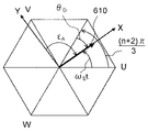
この補正処理のより具体的な実現方法について説明する。a1軸〜a6軸の内、電圧ベクトル110が最も近い軸の位相は、U相軸を基準として、「(n+2)π/3」にて表される。ここで、nは、(θ+ε)をπ/3で割った時に得られる商である。便宜上、図10に示す如く、θを、上記の位相(n+2)π/3と、その位相(n+2)π/3とθとの差分位相θDと、に分解する。これらの位相の関係は、式(1−1)及び式(1−2)にて表される。
A more specific method for realizing this correction process will be described. Of the a 1 axis to a 6 axis, the phase of the axis with the

dq座標を差分位相θDだけ座標変換することにより、電圧ベクトル110をab座標上における電圧ベクトルとして捉える。ab座標上で考え、電圧ベクトル110のa軸成分及びb軸成分をa軸電圧va及びb軸電圧vbとすると、d軸電圧vd及びq軸電圧vqとa軸電圧va及びb軸電圧vbは、下記式(1−3)の座標変換式を満たす。
By converting the dq coordinate by the difference phase θ D , the
差分位相θDは、以下のように算出できる。下記式(1−4)を用いて算出されるεに合致するn(即ち、(θ+ε)をπ/3で割った時に得られる商)を、θを参照して求める。その求めたnとθを上記式(1−2)に代入すれば、差分位相θDが得られる。 The differential phase θ D can be calculated as follows. The value n (that is, the quotient obtained by dividing (θ + ε) by π / 3) that matches ε calculated using the following equation (1-4) is obtained with reference to θ. By substituting the obtained n and θ into the above equation (1-2), the differential phase θ D can be obtained.
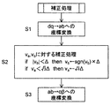
そして、式(1−3)に従って算出されたa軸電圧va及びb軸電圧vbを参照して補正処理を行う。図11に、この補正処理の手順を示すフローチャートを示す。ステップS1では、式(1−3)に従う座標変換が行われる。続くステップS2において、va及びvbに対する補正処理が行われる。 Then, correction processing is performed with reference to the a-axis voltage v a and the b-axis voltage v b calculated according to the equation (1-3). FIG. 11 is a flowchart showing the procedure of the correction process. In step S1, coordinate transformation according to the equation (1-3) is performed. In subsequent step S2, correction processing for v a and v b is performed.
ステップS2では、まず、b軸電圧vbの大きさ(絶対値)が所定の閾値Δ(但し、Δ>0)より小さいか否かを判断する。即ち、下記式(1−5)が満たされるか否かを判断する。そして、b軸電圧vbの大きさが閾値Δより小さい場合であって且つb軸電圧vbが正である場合は、vbがΔとなるように補正する。b軸電圧vbの大きさが閾値Δより小さい場合であって且つb軸電圧vbが負である場合は、vbが(−Δ)となるように補正する。b軸電圧vbの大きさが閾値Δ以上の場合、vbに対して補正は施されない。 In step S2, it is first determined whether or not the magnitude (absolute value) of the b-axis voltage v b is smaller than a predetermined threshold value Δ (where Δ> 0). That is, it is determined whether or not the following formula (1-5) is satisfied. When the b-axis voltage v b is smaller than the threshold value Δ and the b-axis voltage v b is positive, the correction is performed so that v b becomes Δ. When the magnitude of the b-axis voltage v b is smaller than the threshold value Δ and the b-axis voltage v b is negative, the correction is performed so that v b becomes (−Δ). When the b-axis voltage v b is greater than or equal to the threshold Δ, no correction is performed on v b .
また、ステップS2において、a軸電圧vaが下記式(1−6)を満たすか否かも判断する。そして、式(1−6)を満たす場合、vaが式(1−6)の右辺と等しくなるようにvaを補正する。vaが下記式(1−6)を満たさない場合、vaに対して補正は施されない。尚、式(1−6)によって、電圧ベクトル110が図9の円131の内部に含まれるかを判断している。電圧ベクトル110が円131の内部に含まれる状態は、三相の相電圧が互いに接近している状態に対応しており、この状態においては、b軸電圧vbの大きさに関わらず2相分の電流は検出できない。
Further, in step S2, a-axis voltage v a is also determine whether satisfies the following formula (1-6). When satisfying the formula (1-6), v a is corrected v a to be equal to the right side of the equation (1-6). If v a does not satisfy the following formula (1-6), the correction is not performed with respect to v a. It should be noted that whether or not the
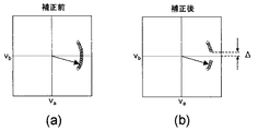
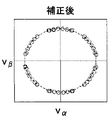
図12に、ステップS2による補正処理の前後の、ab座標上における電圧ベクトル(110)の軌跡を示す。図12(a)は、ab座標上における補正前の電圧ベクトル軌跡を表し、図12(b)は、ab座標上における補正後の電圧ベクトル軌跡を表す。図12(a)及び(b)は、b軸電圧vbが補正される場合を例示している。図12(a)及び(b)の夫々に、各タイミングの電圧を表すプロットが多数記されている。図12(a)に対応する補正前の電圧ベクトルは、2相分の電流を検出不可能なa軸近傍にも位置しうるが、図12(b)に対応する補正後の電圧ベクトルは、vbに対する補正によってa軸近傍に位置することがない。 FIG. 12 shows the locus of the voltage vector (110) on the ab coordinate before and after the correction process in step S2. FIG. 12A shows a voltage vector locus before correction on the ab coordinate, and FIG. 12B shows a voltage vector locus after correction on the ab coordinate. FIGS. 12A and 12B illustrate a case where the b-axis voltage v b is corrected. In each of FIGS. 12A and 12B, a large number of plots representing the voltages at each timing are described. The voltage vector before correction corresponding to FIG. 12A can be positioned near the a-axis where current for two phases cannot be detected, but the voltage vector after correction corresponding to FIG. Due to the correction for v b, it is not located near the a-axis.
ステップS2による補正処理の後、ステップS3に移行し、補正後の電圧ベクトル110を「位相(n+2)π/3」だけ座標変換する。即ち、ab座標上における補正後の電圧ベクトル110を、αβ座標上の電圧ベクトル110に変換する。αβ座標(αβ固定座標)は、α軸とα軸に直交するβ軸とを座標軸に選んだ固定座標である。図13に示す如く、α軸はU相軸と一致している。電圧ベクトル110のα軸成分及びβ軸成分をα軸電圧vα及びβ軸電圧vβとすると、α軸電圧vα及びβ軸電圧vβと補正後のa軸電圧va及びb軸電圧vbは、下記式(1−7)の座標変換式を満たす。
After the correction processing in step S2, the process proceeds to step S3, and the corrected
また、補正後のa軸電圧va及びb軸電圧vbを、下記式(1−8)に従ってU相電圧vu及びV相電圧vvに変換することもできる。また、W相電圧vwは、下記式(1−9)に従って算出される。 Further, the corrected a-axis voltage v a and b-axis voltage v b can be converted into a U-phase voltage v u and a V-phase voltage v v according to the following equation (1-8). The W-phase voltage v w is calculated according to the following formula (1-9).
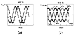
上記の補正処理を経た電圧ベクトルのαβ座標上の軌跡を図14に示す。この補正処理により、固定座標であるαβ座標において、電圧ベクトルが位置しない領域が電気角60度ごとに存在するようになる。また、上記の補正処理を経て得られるvα及びvβの電圧波形を、横軸を時間にとり、図15(a)に示す。また、上記の補正処理を経て得られるvu、vv及びvwの電圧波形を、横軸を時間にとり、図15(b)に示す。図15(b)において、歪んだ正弦波上に並ぶプロット群142uはvuの軌跡を、歪んだ正弦波上に並ぶプロット群142vはvvの軌跡を、歪んだ正弦波上に並ぶプロット群142wはvwの軌跡を表す。図15(b)からも分かるように、上記の補正処理によって各相電圧間の電圧差が所定値以上、確保されている。
FIG. 14 shows the locus on the αβ coordinate of the voltage vector that has undergone the above correction processing. As a result of this correction processing, in the αβ coordinates, which are fixed coordinates, a region where no voltage vector is located exists every electrical angle 60 degrees. FIG. 15A shows the voltage waveforms of vα and vβ obtained through the above correction processing, with the horizontal axis representing time. Further, voltage waveforms of v u , v v, and v w obtained through the above correction processing are shown in FIG. In FIG. 15B, the
このように、本補正手法では、dq座標から固定座標(例えば、αβ座標)へ座標変換する際、ab座標を介して2段階の座標変換を行うようにする。そして、補正のしやすいab座標上において電圧ベクトルに対する補正処理を実行することで、必要な補正を、簡素に且つ確実に実現する。ab座標において、電圧ベクトル(電圧指令ベクトル)の座標軸成分va及びvbを独立して補正するだけで済むため、補正内容が簡素である。特に印加電圧が低い時には3相全てに対して補正が必要となるが、このような場合にも補正量の決定が容易である。 As described above, in this correction method, when the coordinate conversion from the dq coordinate to the fixed coordinate (for example, αβ coordinate) is performed, two-step coordinate conversion is performed via the ab coordinate. Then, by executing a correction process for the voltage vector on the ab coordinates that are easy to correct, the necessary correction is simply and reliably realized. In the ab coordinates, since only have to independently corrected coordinate axis component v a and v b of the voltage vector (specified voltage vector), the correction contents are simple. In particular, when the applied voltage is low, correction is required for all three phases. In such a case, the correction amount can be easily determined.
尚、この2段階の座標変換と、dq座標とαβ座標との座標変換(通常の1段階の座標変換)とが等価であること、即ち下記式(1−10)が成立することは、上記式(1−2)より明らかである。 It is to be noted that the two-step coordinate transformation is equivalent to the coordinate transformation (ordinary one-step coordinate transformation) between the dq coordinate and the αβ coordinate, that is, the following formula (1-10) is satisfied. It is clear from the equation (1-2).
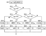
また、ステップS2でのb軸電圧vbに対する補正処理において、過去の補正を考慮して補正を行うようにしてもよい。この過去の補正を考慮した、vbに対する補正処理を、図16を参照して説明する。図16は、この補正処理の手順を示すフローチャートである。 Further, in the correction process for the b-axis voltage v b in step S2, it may be performed correction in consideration of the past correction. A correction process for v b in consideration of the past correction will be described with reference to FIG. FIG. 16 is a flowchart showing the procedure of the correction process.
モータ駆動システム内において、vbの値は所定のサンプリング周期Tsにて逐次更新されていく。vbをサンプリング周期Tsにて離散化して考え、各サンプリング周期Tsにおけるvbをvb(k)、vb(k−1)、vb(k−2)、・・・と表記する。また、変数Δbを定義し、各サンプリング周期Tsにおける変数ΔbをΔb(k)、Δb(k−1)、Δb(k−2)、・・・と表記する。 In the motor drive system, the value of v b is sequentially updated at a predetermined sampling period T s . v b is discretized at the sampling period T s, and v b at each sampling period T s is expressed as v b (k), v b (k−1), v b (k−2),. To do. Further, a variable Δb is defined, and the variable Δb in each sampling period T s is expressed as Δb (k), Δb (k−1), Δb (k−2),.
カッコ“( )”内に表記される記号(kまたは(k−1)など)は、サンプリング周期Tsで離散化した場合のサンプリングタイミングを表している。kは自然数であり、(k)は、(k−1)の次に訪れるサンプリングタイミングを表す。vb(k)及びΔb(k)は、k番目のサンプリングタイミングにおけるvb及びΔbであり、vb(k−1)及びΔb(k−1)は、(k−1)番目のサンプリングタイミングにおけるvb及びΔbである。尚、サンプリング周期TSは、キャリア信号のキャリア周期(図4参照)の整数倍とされる。キャリア周期が1/(10×103)[秒]の場合、TSは、例えば、1/(10×103)、1/(5×103)又は1/(2.5×103)[秒]とされる。 Symbols in parentheses “()” (such as k or (k−1)) represent sampling timings when discretized at the sampling period T s . k is a natural number, and (k) represents a sampling timing that comes next to (k−1). v b (k) and Δb (k) are v b and Δb at the k th sampling timing, and v b (k−1) and Δb (k−1) are the (k−1) th sampling timing. V b and Δb. Note that the sampling period T S is an integral multiple of the carrier period of the carrier signal (see FIG. 4). When the carrier period is 1 / (10 × 10 3 ) [seconds], T S is, for example, 1 / (10 × 10 3 ), 1 / (5 × 10 3 ), or 1 / (2.5 × 10 3). ) [Seconds].
図16は、k番目のサンプリングタイミングに着目したフローチャートである。まず、ステップS11において、今回の補正前のvb(k)から前回の補正を考慮した変数Δb(k−1)を差し引いた値を変数vbbに代入する。そして、ステップS12において、変数vbbが正であるかを判断する。変数vbbが正である場合はステップS13に移行し、変数vbbが負(或いはゼロ)である場合はステップS23に移行する。 FIG. 16 is a flowchart focusing on the kth sampling timing. First, in step S11, a value obtained by subtracting the variable Δb (k−1) considering the previous correction from v b (k) before the current correction is substituted into the variable v bb . In step S12, it is determined whether the variable v bb is positive. When the variable v bb is positive, the process proceeds to step S13, and when the variable v bb is negative (or zero), the process proceeds to step S23.
ステップS13では、変数vbbと上記の閾値Δ(式(1−5)など参照)を比較し、不等式「vbb<Δ」が成立する場合はステップS14に移行する一方、該不等式が不成立の場合はステップS16に移行する。ステップS14に移行した場合は、閾値ΔからステップS11で算出した変数vbbを差し引いた値を変数Δb(k)に代入し、続くステップS15において、閾値Δをvb(k)に代入する。他方、ステップS16に移行した場合は、変数Δb(k)にゼロを代入し、続くステップS17において変数vbbをvb(k)に代入する。ステップS15又はS17の処理を終えると図16の処理は終了する。 In step S13, the variable v bb is compared with the threshold value Δ (see equation (1-5) etc.), and if the inequality “v bb <Δ” is satisfied, the process proceeds to step S14, while the inequality is not satisfied. In this case, the process proceeds to step S16. When the process proceeds to step S14, a value obtained by subtracting the variable v bb calculated in step S11 from the threshold value Δ is substituted into the variable Δb (k), and in step S15, the threshold value Δ is substituted into v b (k). On the other hand, when the process proceeds to step S16, zero is substituted for the variable Δb (k), and in the subsequent step S17, the variable v bb is substituted for v b (k). When the process of step S15 or S17 is completed, the process of FIG. 16 ends.
ステップS23では、変数vbbと(−Δ)を比較し、不等式「vbb>−Δ」が成立する場合はステップS24に移行する一方、該不等式が不成立の場合はステップS26に移行する。ステップS24に移行した場合は、(−Δ)からステップS11で算出した変数vbbを差し引いた値を変数Δb(k)に代入し、続くステップS25において、(−Δ)をvb(k)に代入する。他方、ステップS26に移行した場合は、変数Δb(k)にゼロを代入し、続くステップS27において変数vbbをvb(k)に代入する。ステップS25又はS27の処理を終えると図16の処理は終了する。 In step S23, the variable v bb is compared with (−Δ), and if the inequality “v bb > −Δ” is satisfied, the process proceeds to step S24, whereas if the inequality is not satisfied, the process proceeds to step S26. When the process proceeds to step S24, the value obtained by subtracting the variable v bb calculated in step S11 from (−Δ) is substituted into the variable Δb (k), and in step S25, (−Δ) is replaced with v b (k). Assign to. On the other hand, when the process proceeds to step S26, zero is substituted for the variable Δb (k), and in the subsequent step S27, the variable v bb is substituted for v b (k). When the process of step S25 or S27 is completed, the process of FIG. 16 ends.
図16のステップS15、S17、S25又はS27の処理を経て得られたvb(k)は、今回の補正後のb軸電圧vbとして取り扱われる(但し、実際の補正が施されない場合もある)。ステップS14、S16、S24又はS26の処理を経て得られた変数Δb(k)は、(k+1)番目のサンプリングタイミングにおけるvbの補正処理に利用される。 V b (k) obtained through the processing of step S15, S17, S25 or S27 in FIG. 16 is handled as the b-axis voltage v b after the current correction (however, actual correction may not be performed). ). The variable Δb (k) obtained through the process of step S14, S16, S24 or S26 is used for the correction process of v b at the (k + 1) th sampling timing.
図8等の電圧ベクトル110が領域111外に位置するようにvbに対して補正を行うことにより、図15(b)に示す如く各相電圧が不連続となってしまう。図17に、この不連続部分における電圧(例えばvu)の様子を示す。この不連続性は、モータ1の滑らかな駆動にとって望ましいものではない。
By correcting v b so that the
補正が必要な期間において(即ち、式(1−5)が満たされる期間において)、上述のステップS2(図11参照)の如く、単純に、vbが正ならvbにΔを代入し且つvbが負ならvbに(−Δ)を代入する手法を採用すれば、その不連続性は比較的大きくなるが、図16に示すような過去の補正を考慮した補正処理を実施することによって、vbがΔと(−Δ)との間を行ったりきたりする。この結果、例えば図18に示すように、電圧の不連続部分で電圧(例えばvu)がPWM変調されるかのように変動することになり、電圧の不連続性が緩和される。 The correction is required period (i.e., formula (in the period in which 1-5) is satisfied), as described above in step S2 (see FIG. 11), simply, v b is substituted for Δ to positive if v b and If v b is negative, if a method of substituting (−Δ) into v b is adopted, the discontinuity becomes relatively large, but correction processing considering past correction as shown in FIG. 16 is performed. , V b may go between Δ and (−Δ). As a result, for example, as shown in FIG. 18, the voltage (for example, v u ) fluctuates as if it is PWM-modulated at the voltage discontinuity portion, and the voltage discontinuity is alleviated.
以下に、上述の補正処理(補正手法)を適用した実施例として、第1〜第5実施例を例示する。尚、或る実施例(例えば第1実施例)に記載した事項は、矛盾なき限り、他の実施例にも適用される。 Below, the 1st-5th Example is illustrated as an Example to which the above-mentioned correction process (correction method) is applied. The matters described in a certain embodiment (for example, the first embodiment) can be applied to other embodiments as long as there is no contradiction.
<<第1実施例>>
まず、第1実施例について説明する。図19は、第1実施例に係るモータ駆動システムの全体構成ブロック図である。図19において、図1と同一の部分には同一の符号を付す。
<< First Example >>
First, the first embodiment will be described. FIG. 19 is a block diagram of the overall configuration of the motor drive system according to the first embodiment. In FIG. 19, the same parts as those in FIG.
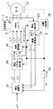
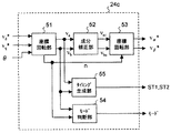
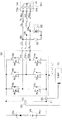
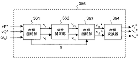
図19のモータ駆動システムは、モータ1、インバータ2、直流電源4及び電流センサ5を備えていると共に、図1の制御部3を形成する「電流検出部21、座標変換器22、電圧演算部23、電圧ベクトル補正部24、座標変換器25、位置センサ27、位置検出部28及び微分器29」を備えている。
The motor drive system of FIG. 19 includes a
位置センサ27は、ロータリエンコーダ等であり、モータ1の回転子6の実回転子位置θ(位相)に応じた信号を位置検出部28に送る。位置検出部28は、位置センサ27の出力信号に基づいて実回転子位置θを検出する。微分器29は、その実回転子位置θを微分することにより、実モータ速度ωを算出して出力する。
The
上述の如く、電流センサ5は、母線電流を検出し該母線電流の電流値を表す信号を出力する。母線電流をidcにて表す。電流検出部21は、座標変換器25が出力する三相電圧指令値vu *、vv *及びvw *を参照して、何れの相が最大相、中間相及び最小相であるかを特定すると共に電流センサ5の出力信号をサンプリングするタイミングST1及びST2(図6参照)を決定し、そのタイミングにおいて得た母線電流の電流値からU相電流iu及びV相電流ivを算出及び出力する。この際、必要に応じて、iu+iv+iw=0、の関係式を用いる(iwはW相電流を表す)。
As described above, the
座標変換器22は、実回転子位置θに基づいてU相電流iu及びV相電流ivをd軸電流id及びq軸電流iqに変換して出力する。
The coordinate
電圧演算部23には、外部から、モータ1(回転子6)を所望の速度で回転させるための指令値としてモータ速度指令値ω*が与えられる。また、電圧演算部23には、微分器29から実モータ速度ωが与えられ、座標変換器22からd軸電流id及びq軸電流iqが与えられる。電圧演算部23は、速度誤差(ω*−ω)に基づいて、q軸電流iqが追従すべきq軸電流指令値iq *を算出する。例えば、比例積分制御によって(ω*−ω)がゼロに収束するようにiq *を算出する。更に、電圧演算部23は、iq *を参照して、d軸電流idが追従すべきd軸電流指令値id *を算出する。例えば、最大トルク制御を実現するためのid *を算出する。そして、電圧演算部23は、電流誤差(id *−id)及び(iq *−iq)がゼロに収束するように比例積分制御を行って、d軸電圧vdが追従すべきd軸電圧指令値vd *及びq軸電圧vqが追従すべきq軸電圧指令値vq *を算出及び出力する。
The
電圧ベクトル補正部24は、vd *及びvq *並びにθに基づき、vd *及びvq *を座標変換を介して補正しつつα軸電圧vαが追従すべきα軸電圧指令値vα*及びβ軸電圧vβが追従すべきβ軸電圧指令値vβ*を算出して出力する。座標変換器25は、実回転子位置θに基づいてvα*及びvβ*を三相電圧指令値(vu *、vv *及びvw *)に変換し、該三相電圧指令値をインバータ2に出力する。インバータ2は、該三相電圧指令値に従って、上述の如く三相交流電流をモータ1に供給する。
Voltage
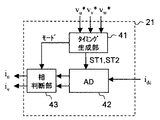
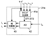
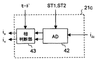
図20に、電流検出部21の内部ブロック図を示す。電流検出部21の動作の説明に、図6も参照される。電流検出部21は、タイミング生成部41と、AD変換器42と、相判断部43と、を有する。図6を参照して説明したように、vu *、vv *及びvw *は、夫々、カウンタの設定値CntU、CntV及びCntWとして表される。タイミング生成部41は、vu *、vv *及びvw *に基づき、カウンタの設定値CntU、CntV及びCntWの大小関係を判断して現時点が第1〜第6モードの何れに属するかを特定すると共に、特定されたモードを考慮して母線電流を検出すべきタイミングST1及びST2を決定する。例えば、「CntU>CntV>CntW」である場合、現時点は第1モードに属すると判断し、設定値CntWとCntVの間に対応するタイミングをST1、設定値CntVとCntUの間に対応するタイミングをST2と定める。
FIG. 20 shows an internal block diagram of the
以下、現時点が属するモードを表す情報を、「モード情報」と呼ぶ。 Hereinafter, information indicating the mode to which the present time belongs is referred to as “mode information”.
AD変換器42は、タイミングST1とST2の夫々において電流センサ5の出力信号(アナログ出力信号)をサンプリングすることにより、タイミングST1とST2の夫々における母線電流idcの電流値をデジタル値として検出及び出力する。相判断部43は、タイミング生成部41にて特定されたモード情報を参照して、AD変換器42の出力信号からiu及びivを算出する。例えば、モード情報が第1モードを表す場合、タイミングST1及びST2にて検出される母線電流は、それぞれ、(−iw)及びiuである。iu+iv+iw=0、の関係式を用いれば、iu及びivを算出可能である。
The
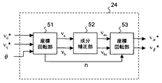
図21に、電圧ベクトル補正部24の内部ブロック図を示す。電圧ベクトル補正部24は、座標回転部51及び53と、成分補正部52と、を有する。電圧ベクトル補正部24では、上記式(1−3)及び(1−4)におけるvd及びvqとしてvd *及びvq *が用いられる。
FIG. 21 shows an internal block diagram of the voltage
座標回転部51は、vd *及びvq *並びにθに基づき、上記式(1−3)に従って、vd *及びvq *をva及びvbに変換する。つまり、vd *及びvq *によって表される、dq座標上の2相の電圧指令ベクトルを、va及びvaによって表される、ab座標上の2相の電圧指令ベクトルに変換する(これらの電圧指令ベクトルは、図8の電圧ベクトル110に相当する)。
The coordinate
式(1−3)に基づく演算を実施する上で差分位相θDが必要となるが、差分位相θDは、式(1−4)を参照して上述した手法を用いて算出される。また、差分位相θDを算出する際に座標回転部51にて求められたnは、座標回転部53での演算に利用される。
The differential phase θ D is required to perform the calculation based on the equation (1-3), and the differential phase θ D is calculated using the method described above with reference to the equation (1-4). In addition, n obtained by the coordinate
成分補正部52は、図11のステップS2における補正処理又は図16に示す補正処理をva及びvbに対して施し、補正後のva及びvbを、夫々vac及びvbcとして出力する。但し、補正が不要の場合は、vac=va且つvbc=vb、となる。
座標回転部53は、上記式(1−7)に従って、補正後のa軸電圧及びb軸電圧(即ちvac及びvbc)をvα*及びvβ*に変換する。つまり、vac及びvbcによって表される、ab座標上の2相の電圧指令ベクトルを、vα*及びvβ*によって表される、αβ座標(αβ固定座標)上の2相の電圧指令ベクトルに変換する。この際、式(1−7)におけるva、vb、vα及びvβとして、それぞれvac、vbc、vα*及びvβ*が用いられる。
The coordinate
第1実施例では、vu *、vv *及びvw *の大小関係に基づいて現時点が属するモードを特定することにより、タイミングST1及びST2において母線電流として母線13(図1参照)に流れる電流の相を判断する。そして、その判断結果(即ち、モード情報)に従って、vu *、vv *及びvw *からタイミングST1及びST2を決定する。 In the first embodiment, by specifying the mode to which the present time belongs based on the magnitude relationship among v u * , v v *, and v w * , the current flows to the bus 13 (see FIG. 1) as the bus current at timings ST1 and ST2. Determine the phase of the current. Then, timings ST1 and ST2 are determined from v u * , v v *, and v w * according to the determination result (that is, mode information).
<<第2実施例>>
次に、第2実施例について説明する。図22は、第2実施例に係るモータ駆動システムの全体構成ブロック図である。図22において、図1及び図19と同一の部分には同一の符号を付す。
<< Second Example >>
Next, a second embodiment will be described. FIG. 22 is a block diagram of the overall configuration of the motor drive system according to the second embodiment. In FIG. 22, the same parts as those in FIGS. 1 and 19 are denoted by the same reference numerals.
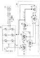
図22のモータ駆動システムは、モータ1、インバータ2、直流電源4及び電流センサ5を備えていると共に、図1の制御部3を形成する「電流検出部21a、座標変換器22、電圧演算部23、電圧ベクトル補正部24a、座標変換器25、位置センサ27、位置検出部28及び微分器29」を備えている。
The motor drive system shown in FIG. 22 includes a
図22のモータ駆動システムは、図19のモータ駆動システムにおける電流検出部21及び電圧ベクトル補正部24が電流検出部21a及び電圧ベクトル補正部24aに置換されている点において図19のモータ駆動システムと相違しており、その他の点において両モータ駆動システムは同様である。相違点に関して詳細に説明する。尚、第1実施例に記載した事項を第2実施例に適用する場合、符号21と21aの相違と符号24と24aの相違は、適宜、無視される。
The motor drive system of FIG. 22 differs from the motor drive system of FIG. 19 in that the
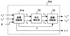
図23に、電圧ベクトル補正部24aの内部ブロック図を示す。電圧ベクトル補正部24aは、座標回転部51a及び53と、成分補正部52と、を有する。電圧ベクトル補正部24aでは、上記式(1−3)及び(1−4)におけるvd及びvqとしてvd *及びvq *が用いられる。
FIG. 23 shows an internal block diagram of the voltage
座標回転部51aは、vd *及びvq *並びにθに基づき、上記式(1−3)に従って、vd *及びvq *をva及びvbに変換する。式(1−3)に基づく演算を実施する上で差分位相θDが必要となるが、差分位相θDは、式(1−4)を参照して上述した手法を用いて算出される。また、差分位相θDを算出する際に座標回転部51aにて求められたnは、座標回転部53での演算に利用される。
The coordinate
更に、座標回転部51aは、vd *及びvq *に基づいて求めたεをも参照して現時点が属するモードを特定し、モード情報を作成する。図24に、座標回転部51aの処理内容をブロック図として示す。図25に、座標回転部51aによるモード特定手法を説明するための表を示す。図6を参照して説明したように、例えば、第1モードにおいては「vu>vv>vw」が成立する。一方、図8を参照して説明したように、U相軸を基準とした電圧ベクトル(電圧指令ベクトル)の位相は(θ+ε+π/2)によって表され、「0<(θ+ε+π/2)<π/3」が成立する場合に、「vu>vv>vw」が成立する。
Furthermore, the coordinate
これを考慮し、座標回転部51aは、θ及びεを参照し、「0<(θ+ε+π/2)<π/3」が成立する場合は、現時点が第1モードに属すると判断する。同様に考えて、現時点は、
「π/3<(θ+ε+π/2)<2π/3」が成立する場合、第2モードに属し、
「2π/3<(θ+ε+π/2)<π」が成立する場合、第3モードに属し、
「π<(θ+ε+π/2)<4π/3」が成立する場合、第4モードに属し、
「4π/3<(θ+ε+π/2)<5π/3」が成立する場合、第5モードに属し、
「5π/3<(θ+ε+π/2)<2π」が成立する場合、第6モードに属すると判断する。
Considering this, the coordinate
If “π / 3 <(θ + ε + π / 2) <2π / 3” holds, it belongs to the second mode,
If “2π / 3 <(θ + ε + π / 2) <π” holds, it belongs to the third mode,
If “π <(θ + ε + π / 2) <4π / 3” holds, it belongs to the fourth mode,
If “4π / 3 <(θ + ε + π / 2) <5π / 3” holds, it belongs to the fifth mode,
When “5π / 3 <(θ + ε + π / 2) <2π” is satisfied, it is determined that the mode belongs to the sixth mode.
図23における成分補正部52及び座標回転部53は、図21におけるそれらと同じものである。
The
図26に、電流検出部21aの内部ブロック図を示す。電流検出部21aは、タイミング生成部41aと、AD変換器42と、相判断部43と、を有する。タイミング生成部41aは、vu *、vv *及びvw *に基づき、電圧ベクトル補正部24aにて作成されたモード情報を考慮して母線電流を検出すべきタイミングST1及びST2を決定する。電圧ベクトル補正部24aからモード情報が与えられるため、第1実施例(図20)のタイミング生成部41と異なり、タイミング生成部41aにてモードを特定するための判断を行う必要はない。
FIG. 26 shows an internal block diagram of the
図26におけるAD変換器42及び相判断部43は、図20におけるそれらと同じのものである。但し、図26の相判断部43に対し、モード情報は、電圧ベクトル補正部24aから与えられる。
The
第2実施例では、U相軸を基準とした電圧指令ベクトルの位相(θ+ε+π/2)に基づいて現時点が属するモードを特定することにより、タイミングST1及びST2において母線電流として母線13(図1参照)に流れる電流の相を判断する。そして、その判断結果(即ち、モード情報)に従って、vu *、vv *及びvw *からタイミングST1及びST2を決定する。 In the second embodiment, by specifying the mode to which the present time belongs based on the phase (θ + ε + π / 2) of the voltage command vector with reference to the U-phase axis, the bus 13 (see FIG. 1) is used as the bus current at the timings ST1 and ST2. ) Is determined. Then, timings ST1 and ST2 are determined from v u * , v v *, and v w * according to the determination result (that is, mode information).
<<第3実施例>>
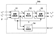
次に、第3実施例について説明する。第3実施例に係るモータ駆動システムの全体構成ブロック図は、第2実施例(図22)におけるそれと同様である。但し、第3実施例における電圧ベクトル補正部は、第2実施例におけるそれと異なる。第3実施例における電圧ベクトル補正部24bの内部ブロック図を図27に示す。第3実施例では、図22の電圧ベクトル補正部24aが電圧ベクトル補正部24bにて置き換えられる。電圧ベクトル補正部24bは、図26の電流検出部21aと組み合わせて用いられる。
<< Third Example >>
Next, a third embodiment will be described. The overall configuration block diagram of the motor drive system according to the third embodiment is the same as that in the second embodiment (FIG. 22). However, the voltage vector correction unit in the third embodiment is different from that in the second embodiment. FIG. 27 shows an internal block diagram of the voltage
電圧ベクトル補正部24bは、座標回転部51及び53と、成分補正部52と、モード判断部54と、を有する。電圧ベクトル補正部24bでは、上記式(1−3)及び(1−4)におけるvd及びvqとしてvd *及びvq *が用いられる。
The voltage
座標回転部51及び53並びに成分補正部52は、図21におけるそれらと同じものである。座標回転部51にて算出されたn及びvbは、モード判断部54に送られる。
The coordinate
モード判断部54は、vb及びnに基づいて現時点が属するモードを特定してモード情報を作成し、該モード情報を電流検出部21a(図22)に送る。図28に、モード判断部54によるモード特定手法を説明するための表を示す。
The
図6を参照して説明したように、例えば、第1モードにおいては「vu>vv>vw」が成立する。一方、「3π/2<(θ+ε)<11π/6」が成立する場合に、「vu>vv>vw」が成立する。また、「3π/2<(θ+ε)<5π/3」が成立する場合は、n=4且つvb>0であり、「5π/3<(θ+ε)<11π/6」が成立する場合は、n=5且つvb<0である。 As described with reference to FIG. 6, for example, “v u > v v > v w ” is established in the first mode. On the other hand, when “3π / 2 <(θ + ε) <11π / 6” is satisfied, “v u > v v > v w ” is satisfied. When “3π / 2 <(θ + ε) <5π / 3” is satisfied, n = 4 and v b > 0, and when “5π / 3 <(θ + ε) <11π / 6” is satisfied. , N = 5 and v b <0.
このような関係を考慮し、モード判断部54は、vbの極性とnの値に基づいて現時点が属するモードを特定する。具体的には、現時点は、
n=4且つvb>0の場合或いはn=5且つvb<0の場合、第1モードに属し、
n=5且つvb>0の場合或いはn=0且つvb<0の場合、第2モードに属し、
n=0且つvb>0の場合或いはn=1且つvb<0の場合、第3モードに属し、
n=1且つvb>0の場合或いはn=2且つvb<0の場合、第4モードに属し、
n=2且つvb>0の場合或いはn=3且つvb<0の場合、第5モードに属し、
n=3且つvb>0の場合或いはn=4且つvb<0の場合、第6モードに属すると判断する。
In consideration of such a relationship, the
If n = 4 and v b > 0, or if n = 5 and v b <0, they belong to the first mode,
If n = 5 and v b > 0, or if n = 0 and v b <0, they belong to the second mode,
If n = 0 and v b > 0, or if n = 1 and v b <0, they belong to the third mode,
If n = 1 and v b > 0, or if n = 2 and v b <0, they belong to the fourth mode,
If n = 2 and v b > 0, or if n = 3 and v b <0, they belong to the fifth mode,
If n = 3 and v b > 0, or if n = 4 and v b <0, it is determined to belong to the sixth mode.
第3実施例では、ab座標上における2相の電圧指令ベクトルの座標軸成分であるvbと、ab座標の座標軸(a軸)とU相軸との位相差を電気角60度を単位として表した変数nと、に基づいて現時点が属するモードを特定し、これによってタイミングST1及びST2において母線電流として母線13(図1参照)に流れる電流の相を判断する。そして、その判断結果(即ち、モード情報)に従って、vu *、vv *及びvw *からタイミングST1及びST2を決定する。 In the third embodiment, the phase difference between the coordinate axis component v b of the two-phase voltage command vector on the ab coordinate and the coordinate axis (a axis) of the ab coordinate and the U phase axis is expressed in units of 60 electrical angles. Based on the variable n, the mode to which the present time belongs is specified, and thereby the phase of the current flowing through the bus 13 (see FIG. 1) as the bus current is determined at the timings ST1 and ST2. Then, timings ST1 and ST2 are determined from v u * , v v *, and v w * according to the determination result (that is, mode information).
<<第4実施例>>
次に、第4実施例について説明する。第4実施例では2相変調を用いる。このため、3相変調を前提として上述してきた内容の一部(図4に示すPWM信号など)は、第4実施例において、適宜変更して解釈される。今、dq座標、ab座標又はαβ座標における電圧ベクトル(電圧指令ベクトル)の大きさをVa2とし、その電圧ベクトルを3相電圧に変換した時の1相の電圧の振幅をVa3とすると、下記式(2−1)が成り立つ。
<< 4th Example >>
Next, a fourth embodiment will be described. In the fourth embodiment, two-phase modulation is used. For this reason, a part of the content described above on the premise of three-phase modulation (such as the PWM signal shown in FIG. 4) is interpreted as appropriately changed in the fourth embodiment. Now, let V a2 be the magnitude of the voltage vector (voltage command vector) in the dq coordinate, ab coordinate, or αβ coordinate, and let V a3 be the amplitude of one-phase voltage when the voltage vector is converted into a three-phase voltage. The following formula (2-1) is established.
![]()
![]()
また、3相の電圧の内の2相の電圧が交差するとき、交差している2相の電圧が「+(1/2)・Va3」であって且つ交差しない残りの1相の電圧が「−Va3」であるか、或いは、交差している2相の電圧が「−(1/2)・Va3」であって且つ交差しない残りの1相の電圧が「+Va3」である。このため、2相の電圧が交差するとき、交差する2相の電圧と残りの1相の電圧との電圧差の絶対値は、(3/2)・Va3、である。 Further, when two-phase voltages among the three-phase voltages intersect, the intersecting two-phase voltages are “+ (1/2) · V a3 ” and the remaining one-phase voltages that do not intersect Is “−V a3 ”, or the crossing two-phase voltage is “− (1/2) · V a3 ” and the remaining one-phase voltage not crossing is “+ V a3 ”. is there. Therefore, when the two-phase voltages intersect, the absolute value of the voltage difference between the intersecting two-phase voltages and the remaining one-phase voltage is (3/2) · V a3 .
2相変調は、3相の電圧の最小相の電圧だけ各相の電圧(指令電圧)をシフトする変調方式であり、2相変調を行うと、最小相に対するPWM信号のパルス幅は常にゼロとなる(即ち、最小相に対する下アームが常にオンとなる)。2相変調を行う場合におけるU相電圧、V相電圧及びW相電圧を、それぞれvu '、vv '及びvw 'とした場合、それらと3相変調を行う場合におけるvu *、vv *及びvw *との関係は、下記式(2−2)、(2−3)及び(2−4)によって表される。ここで、min(vu *,vv *,vw *)は、最小相の電圧、即ち、3相変調を行う場合におけるvu *、vv *及びvw *の内の最小値を表す。 Two-phase modulation is a modulation method in which the voltage (command voltage) of each phase is shifted by the voltage of the minimum phase of the three-phase voltage. When two-phase modulation is performed, the pulse width of the PWM signal for the minimum phase is always zero. (Ie, the lower arm for the minimum phase is always on). When the U-phase voltage, the V-phase voltage, and the W-phase voltage when performing two-phase modulation are v u ′ , v v ′, and v w ′ , respectively, v u * and v when performing three-phase modulation with them. The relationship between v * and v w * is expressed by the following formulas (2-2), (2-3), and (2-4). Here, min (v u * , v v * , v w * ) is the minimum phase voltage, that is, the minimum value of v u * , v v *, and v w * when performing three-phase modulation. To express.
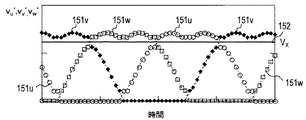
図29に、横軸を時間にとり、vu '、vv '及びvw 'の電圧波形を示す。図29において、丸状のプロット群にて形成される曲線150u、菱形状のプロット群にて形成される曲線150v及び正方形状のプロット群にて形成される曲線150wは、夫々、vu '、vv '及びvw 'の電圧波形を表す。但し、曲線150u、150v及び150wは、図11のステップS2等に示す補正処理を実行していない場合における電圧波形を表す。尚、図29並びに後に示す図30及び図31において、縦軸の長さは、キャリア信号(図4参照)の振幅に相当する。
FIG. 29 shows voltage waveforms of v u ′ , v v ′, and v w ′ with the horizontal axis representing time. In FIG. 29, a curve 150 u formed by a round plot group, a
3相変調を行う場合と同様、vu '、vv '及びvw 'の内の2つの電圧が交差するタイミングでは、2相分の電流を母線電流から検出することはできない。例えば、W相が最小相である場合においてU相電圧とV相電圧が交差するタイミングTAや、最小相がW相からU相に切り替わるタイミングTBでは、2相分の電流を母線電流から検出することはできない。 As in the case of performing the three-phase modulation, the current for two phases cannot be detected from the bus current at the timing when two voltages of v u ′ , v v ′ and v w ′ intersect. For example, the timing T A and W phase crosses the U-phase voltage and the V-phase voltage in the case of the minimum phase, the timing T B minimum phase switches from the W phase to the U phase, the current values of two phases from the bus current It cannot be detected.
最小相から見て他の2相が交差する電圧をVXとする。そうすると、上述の説明から明らかなように、VXは、Va2又はVa3を用いて下記(2−5)のように表される。 A voltage at which the other two phases intersect as seen from the minimum phase is V X. Then, as is clear from the above description, V X is expressed as (2-5) below using V a2 or V a3 .
ここで、式(2−6)が満たされるので、式(2−5)から、式(2−7)、(2−8)及び(2−9)が導かれる。 Here, since Expression (2-6) is satisfied, Expressions (2-7), (2-8), and (2-9) are derived from Expression (2-5).
図30に、横軸を時間にとり、図11のステップS2等に示す補正処理を実行した場合におけるvu '、vv '及びvw 'の電圧波形を示す。図30において、丸状のプロット群にて形成される曲線151u、菱形状のプロット群にて形成される曲線151v及び正方形状のプロット群にて形成される曲線151wは、夫々、上記補正処理が施されたvu '、vv '及びvw 'の電圧波形を表す。図30において、破線152は、電圧VXの電圧レベル(電圧値)を表す。
FIG. 30 shows voltage waveforms of v u ′ , v v ′, and v w ′ when the horizontal axis is time and the correction process shown in step S2 of FIG. 11 is executed. In FIG. 30, a
図30にも表されているように、電圧VXは必ず最大相の電圧と中間相の電圧との間に存在する。従って、電圧VXを用いて母線電流を検出するタイミングを決定することができる。つまり、式(2−7)、(2−8)又は(2−9)から算出される電圧VXに相当するカウンタの設定値CntVXを生成し、カウンタの設定値CntVXを、母線電流から1相分の電流を検出するタイミングとして取り扱えばよい。 As shown in FIG. 30, the voltage V X always exists between the maximum phase voltage and the intermediate phase voltage. Therefore, the timing for detecting the bus current can be determined using the voltage V X. That is, the counter setting value CntV X corresponding to the voltage V X calculated from the equations (2-7), (2-8), or (2-9) is generated, and the counter setting value CntV X is used as the bus current. From this, it can be handled as the timing for detecting the current for one phase.
図4〜図6等を参照して説明したように、制御部3に設けられたカウンタは、キャリア周期ごとに、キャリア信号が最低レベルにあるタイミングを基準としてカウンタ値を0からアップカウントする。このため、各キャリア周期において、そのカウント値がCntVXに達したタイミングにて電流センサ5の出力信号をサンプリングすれば、母線電流を表す該出力信号から最大相の相電流を検出することができる。電圧VXは最大相の電圧と中間相の電圧との間に存在するため、カウント値がCntVXに達したタイミングは、三相変調を行う場合におけるタイミングT2とT3(図4参照)の間のタイミングに対応することになるからである。第4実施例では、カウント値がCntVXに達したタイミングをタイミングST2として取り扱う。
As described with reference to FIGS. 4 to 6 and the like, the counter provided in the
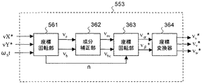
2相変調を行う場合、最小相の下アームが常にオン(最小相のカウンタの設定値がゼロ)とされるため、キャリア信号が最低レベルにあるタイミングは、図4のタイミングT1又はT6に相当することになる。従って、例えば、キャリア信号が最低レベルにあるタイミングにて電流センサ5の出力信号をサンプリングすれば、母線電流を表す該出力信号から最小相の相電流を検出することができる。第4実施例では、キャリア信号が最低レベルにあるタイミング、即ち、カウンタのカウント値がゼロであるタイミングをタイミングST1として取り扱う。
When performing two-phase modulation, the lower arm of the minimum phase is always on (the setting value of the counter of the minimum phase is zero), so the timing at which the carrier signal is at the lowest level corresponds to the timing T1 or T6 in FIG. Will do. Therefore, for example, if the output signal of the
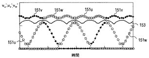
また、電圧VXの計算を簡略化するために、VXを下記式(2−10)のような近似式にて算出することもできる。図31の曲線153は、式(2−10)に従って算出された電圧VXの電圧レベル(電圧値)を表す。図31における曲線151u、151v及び151wは、図30のそれらと同じものである。図31に示す如く、式(2−10)に従って電圧VXを算出したとしても、電圧VXは必ず最大相の電圧と中間相の電圧との間に存在する。従って、式(2−10)から算出される電圧VXに相当するカウンタの設定値をCntVXとして設定するようにしても良い。
Further, in order to simplify the calculation of the voltage V X , V X can be calculated by an approximate expression such as the following expression (2-10). A
![]()
![]()
また、リンギング(スイッチングに由来して生じる電流脈動)等の存在を考慮すると、電流センサ5の出力信号をサンプリングするタイミングは、なるだけ、インバータ2内のスイッチング素子のスイッチングタイミングから離れていた方がよい。このため、補正幅に対応するΔ(上記式(1−5)等参照)を考慮して、式(2−7)、(2−8)、(2−9)又は(2−10)に基づいて決定されるCntVXに補正を加えるようにしてもよい。
Further, in consideration of the presence of ringing (current pulsation caused by switching) or the like, the timing for sampling the output signal of the
上述の電圧VXの算出を利用した、モータ駆動システムの全体構成ブロック図を図32に示す。図32において、図1及び図19と同一の部分には同一の符号を付す。 FIG. 32 shows a block diagram of the overall configuration of the motor drive system using the calculation of the voltage V X described above. 32, the same symbols are added to the same portions as FIG. 1 and FIG.
図22のモータ駆動システムは、モータ1、インバータ2、直流電源4及び電流センサ5を備えていると共に、図1の制御部3を形成する「電流検出部21c、座標変換器22、電圧演算部23、電圧ベクトル補正部24c、座標変換器25、位置センサ27、位置検出部28及び微分器29」を備えている。
The motor drive system of FIG. 22 includes a
図32のモータ駆動システムは、図19のモータ駆動システムにおける電流検出部21及び電圧ベクトル補正部24が電流検出部21c及び電圧ベクトル補正部24cに置換されている点において図19のモータ駆動システムと相違しており、その他の点において両モータ駆動システムは同様である。相違点に関して詳細に説明する。尚、第1実施例に記載した事項を第4実施例に適用する場合、符号21と21cの相違と符号24と24cの相違は、適宜、無視される。
The motor drive system of FIG. 32 differs from the motor drive system of FIG. 19 in that the
図32のモータ駆動システムでは2相変調が行われる。3相変調を行う場合におけるvu *、vv *及びvw *が式(2−2)〜式(2−4)に従ってvu '、vv '及びvw 'に変換され、これらのvu '、vv '及びvw 'が2相変調におけるvu *、vv *及びvw *とされる。図32の座標変換部25からは、この2相変調におけるvu *、vv *及びvw *がインバータ2に与えられる。
In the motor drive system of FIG. 32, two-phase modulation is performed. V u * , v v *, and v w * in the case of performing three-phase modulation are converted into v u ′ , v v ′, and v w ′ according to equations (2-2) to (2-4). v u ′ , v v ′, and v w ′ are v u * , v v *, and v w * in the two-phase modulation. From the coordinate
図33に、電圧ベクトル補正部24cの内部ブロック図を示す。電圧ベクトル補正部24cは、座標回転部51及び53と、成分補正部52と、モード判断部54と、タイミング生成部55と、を有する。つまり、電圧ベクトル補正部24cは、図27の電圧ベクトル補正部24bにタイミング生成部55を追加したものであり、この追加を除いて、両電圧ベクトル補正部は同様のものである。
FIG. 33 shows an internal block diagram of the voltage
尚、本実施例では、第3実施例と同様、モード判断部54を設けてモード情報を作成しているが、現時点が属するモードを特定するための手法として、第1又は第2実施例で説明した手法を用いるようにしてもよい。
In this embodiment, as in the third embodiment, the
タイミング生成部55は、座標回転部51からのva及びvbを用い或いはvaのみを用い、上記式(2−7)又は式(2−10)に従って電圧VXを算出する。そして、算出した電圧VXに相当するカウンタの設定値CntVXを設定する。この設定によってタイミングST2が定まり、また、上述したように、カウント値が0であるタイミングがタイミングST1とされる。
The
また、vd *及びvq *を式(2−8)におけるvd及びvqとして用いつつ、式(2−8)に従って電圧VXを算出するようにしてもよい。また、vd *及びvq *をαβ座標上に変換して(即ち、θだけ座標回転させて)電圧ベクトルのα軸成分及びβ軸成分を算出し、このα軸成分及びβ軸成分を式(2−9)におけるvα及びvβとして用いつつ、式(2−9)に従って電圧VXを算出するようにしてもよい。 Further, the voltage V X may be calculated according to the equation (2-8) while using v d * and v q * as the v d and v q in the equation (2-8). Further, v d * and v q * are converted to αβ coordinates (that is, the coordinates are rotated by θ) to calculate the α-axis component and β-axis component of the voltage vector, and the α-axis component and β-axis component are calculated. The voltage V X may be calculated according to the equation (2-9) while being used as vα and vβ in the equation (2-9).
図34に、電流検出部21cの内部ブロック図を示す。電流検出部21cは、AD変換器42及び相判断部43から成り、図20のタイミング生成部41のようなタイミングST1及びST2を決定する部位を備えていない。電流検出部21cのAD変換器42は、図33のタイミング生成部55にて決定されたタイミングST2及びST1の夫々において、即ち、カウント値が設定値CntVXとなるタイミングと0となるタイミングの夫々において、電流センサ5の出力信号(アナログ出力信号)をサンプリングし、これによってタイミングST1とST2の夫々における母線電流の電流値をデジタル値として検出及び出力する。相判断部43は、タイミング生成部55にて特定されたモード情報を参照して、AD変換器42の出力信号からiu及びivを算出する。
FIG. 34 shows an internal block diagram of the
第4実施例では、電圧ベクトル(電圧指令ベクトル)の大きさに基づいて、電流センサ5の出力信号をサンプリングするタイミングが決定される。また、ab座標上の電圧ベクトルのa軸成分から、該タイミングを決定することも可能である。
In the fourth embodiment, the timing for sampling the output signal of the
<<第5実施例>>
第1〜第4実施例では、回転子位置検出用の位置センサ27が設けられたモータ駆動システムを取り扱ったが、上述した全ての内容は、位置センサ27が設けられていない場合、即ち、所謂センサレス制御を実行する場合にも適用可能である。例として、図22及び図32に示すモータ駆動システムにセンサレス制御を適用した実施例を、第5実施例として説明する。図22及び図32に対応する、第5実施例に係るモータ駆動システムの全体ブロック図を、夫々、図35及び図36に示す。
<< 5th Example >>
In the first to fourth embodiments, the motor drive system provided with the
図35のモータ駆動システムは、「図22のモータ駆動システムにおける位置センサ27、位置検出部28及び微分器29」を「速度推定器30及び積分器31」に置換した点において図22のモータ駆動システムと相違しており、その他の点において両モータ駆動システムは同様である。図36のモータ駆動システムは、「図32のモータ駆動システムにおける位置センサ27、位置検出部28及び微分器29」を「速度推定器30及び積分器31」に置換した点において図32のモータ駆動システムと相違しており、その他の点において両モータ駆動システムは同様である。
The motor drive system of FIG. 35 is different from the motor drive system of FIG. 22 in that “
但し、図35及び図36のモータ駆動システムでは、位置センサが設けられていないため、適宜、上述の説明文及び各式における「d」、「q」、「θ」及び「ω」は、夫々「γ」、「δ」、「θe」及び「ωe」に読み替えられる。 However, since the position sensor is not provided in the motor drive system of FIG. 35 and FIG. 36, “d”, “q”, “θ”, and “ω” in the above description and each expression are appropriately It is read as “γ”, “δ”, “θ e ”, and “ω e ”.
従って、図35又は図36において、座標変換器22は、推定回転子位置θeに基づいてiu及びivをiγ及びiδに変換し、座標変換器25は、推定回転子位置θeに基づいてvα*及びvβ*を三相電圧指令値(vu *、vv *及びvw *)に変換し、電圧演算部23は、iγ及びiδ並びにω*及び推定モータ速度ωeに基づいて、iγ及びiδが追従すべきγ軸電流指令値iγ*及びδ軸電流指令値iδ*を算出し、更にvγ及びvδが追従すべきγ軸電圧指令値vγ*及びδ軸電圧指令値vδ*を算出する。勿論、図35又は図36において、電圧ベクトル補正部24a又は24cは、vd *及びvq *並びにθの代わりにvγ*及びvδ*並びにθeを用いて、上述と同様の補正処理を行う。
Therefore, in FIG. 35 or FIG. 36, a coordinate
速度推定器30は、iγ、iδ、vγ*及びvδ*の全部又は一部を用いて、推定モータ速度ωeを算出する。ωeの算出法として様々な手法が知られており、その何れをも用いることができる。例えば、iγ、iδ、vγ*及びvδ*を用いてモータ1内に生じる誘起電圧を見積もることにより軸誤差Δθを算出し、軸誤差Δθがゼロに収束するように比例積分制御を行うことによりωeを算出する。積分器31は、ωeを積分することによりθeを算出する。
各実施例では、2相分の電流を検出できない領域に電圧ベクトル(電圧指令ベクトル)が位置する場合、回転座標から3相の固定座標へ座標変換する過程において、電圧ベクトルが該領域外に位置するように電圧ベクトルを補正する。これにより、確実にモータ電流(各相電流)を検出することができる。モータ1の回転の停止状態又は低速状態においても確実にモータ電流を検出できるため、停止状態からのモータ駆動が確実に行えるようになり、特に、モータにて駆動する電動車(Electric Vehicle;電動バイクを含む)等において滑らかな始動を実現できる。尚、上記特許文献2のように電流の推定を行う方式を採用すると、検出ではなく推定を行うが故に、ベクトル制御に用いる電流値に多少なりとも誤差が含まれることになる。この誤差は、滑らかな始動にとって好ましくない。
In each embodiment, when a voltage vector (voltage command vector) is located in an area where current for two phases cannot be detected, the voltage vector is located outside the area in the process of coordinate conversion from rotational coordinates to three-phase fixed coordinates. Correct the voltage vector to As a result, the motor current (each phase current) can be reliably detected. Since the motor current can be reliably detected even when the rotation of the
また、電圧ベクトル(電圧指令ベクトル)の座標軸成分va及びvbを独立して補正するだけで済むため、補正内容が簡素である。特に印加電圧が低い時には3相全てに対して補正が必要となるが、このような場合にも補正量の決定が容易である。 Moreover, since only have to independently corrected coordinate axis component v a and v b of the voltage vector (specified voltage vector), the correction contents are simple. In particular, when the applied voltage is low, correction is required for all three phases. In such a case, the correction amount can be easily determined.
本発明を適用したモータ駆動システムの実施例を上述したが、本発明は、様々な変形例(又は他の実施例)を含む。以下に、第1実施形態に対する変形例(又は他の実施例)又は注釈事項として、注釈1〜注釈5を記す。各注釈に記載した内容は、矛盾なき限り、任意に組み合わせることが可能である。 Although the embodiments of the motor drive system to which the present invention is applied have been described above, the present invention includes various modifications (or other embodiments). Below, notes 1 to 5 are described as modifications (or other examples) or annotations to the first embodiment. The contents described in each comment can be arbitrarily combined as long as there is no contradiction.
[注釈1]
第4実施例を除き、インバータ2にて3相変調を用いる場合を取り扱ったが、本発明は変調方式に依存しない。例えば、インバータ2にて2相変調を行う場合、通電パターンは、図3に示した3相変調のそれと異なってくる。2相変調では、最小相の下アームが常にオンとされるため、図4におけるタイミングT0−T1間及びT6−T7間に対応する通電パターンが存在しない。しかしながら、結局、タイミングT1−T2間及びT2−T3間に対応する通電パターンにて母線電流を検出するようにすれば、最大相及び最小相の電流を検出できることに変わりはない。
[Note 1]
Except for the fourth embodiment, the case of using the three-phase modulation in the
尚、2相変調を行うことにより、相電圧の基本波成分の振幅を3相変調(正弦波変調)におけるそれよりも拡大することができる。これにより、最大相のパルス幅に対する制限が緩和され、該最大相のパルス幅を最大限に利用可能となる(即ち、パルスのデューティを100%まで拡大することができる)。また、最小相に対するPWM信号のパルス幅は常にゼロとされるため、1相分のスイッチングロスが低減される。 By performing two-phase modulation, the amplitude of the fundamental wave component of the phase voltage can be expanded more than that in three-phase modulation (sine wave modulation). Thereby, the restriction on the pulse width of the maximum phase is relaxed, and the pulse width of the maximum phase can be used to the maximum (that is, the pulse duty can be increased to 100%). Also, since the pulse width of the PWM signal for the minimum phase is always zero, the switching loss for one phase is reduced.
[注釈2]
第1〜第5実施例に示したモータ駆動システムにおいては、補正されたa軸電圧及びb軸電圧を、一旦、α軸電圧及びβ軸電圧に変換し、その後三相電圧に変換している。しかしながら、α軸電圧及びβ軸電圧への変換を省略することも可能である。
[Note 2]
In the motor drive systems shown in the first to fifth embodiments, the corrected a-axis voltage and b-axis voltage are once converted into an α-axis voltage and a β-axis voltage, and then converted into a three-phase voltage. . However, conversion to the α-axis voltage and the β-axis voltage can be omitted.
即ち、図21等の成分補正部52にて算出されたvac及びvbcを、上記式(1−8)及び(1−9)に従って、αβ座標を介することなく、vu *、vv *及びvw *に変換するようにしてもよい。この際、式(1−8)及び(1−9)におけるva及びvb並びにvu、vv及びvwとして、vac及びvbc並びにvu *、vv *及びvw *が用いられる。尚、この場合、図21等の座標回転部53は不要である。
That is, v ac and v bc calculated by the
[注釈3]
また、上述のモータ駆動システムを構成する各部位は、必要に応じてモータ駆動システム内で生成される値の全てを自由に利用可能となっている。
[Note 3]
Moreover, each part which comprises the above-mentioned motor drive system can utilize freely all the values produced | generated within a motor drive system as needed.
[注釈4]
また、制御部3(図1参照)の機能の一部または全部は、例えば汎用マイクロコンピュータ等に組み込まれたソフトウェア(プログラム)を用いて実現される。ソフトウェアを用いて制御部3を実現する場合、制御部3の各部の構成を示すブロック図は機能ブロック図を表すこととなる。勿論、ソフトウェア(プログラム)ではなく、ハードウェアのみによって制御部3を構成しても構わない。
[Note 4]
In addition, part or all of the functions of the control unit 3 (see FIG. 1) is realized by using software (program) incorporated in a general-purpose microcomputer, for example. When the
[注釈5]
また、例えば、制御部3は、モータ制御装置として機能する。モータ制御装置内に、図1等の電流センサ5が含まれていると考えても構わない。また例えば、図19等の電圧演算部23と図21等の座標回転部51(又は51a)は、電圧指令ベクトル作成手段として機能する。また例えば、図21等の成分補正部52は、電圧指令ベクトル補正手段として機能する。また例えば、図19等の座標変換器25は、三相電圧指令値作成手段として機能する。
[Note 5]
For example, the
<<第2実施形態>>
次に、本発明の第2実施形態について説明する。第2実施形態では、上述の第1実施形態で述べた技術を系統連系に利用する。第1実施形態の記載内容は、適宜、第2又は後述の第3実施形態に適用されるが、第1実施形態と異なる点は、第2又は後述の第3実施形態における説明文中で記述される。
<< Second Embodiment >>
Next, a second embodiment of the present invention will be described. In the second embodiment, the technique described in the first embodiment is used for grid interconnection. The description of the first embodiment is applied to the second or third embodiment described later as appropriate, but the differences from the first embodiment are described in the description of the second or third embodiment described later. The
図39は、第2実施形態に係る系統連系システムの全体構成図である。図39の系統連系システムでは、太陽電池で発電した電力を三相式のインバータを用いて三相の系統に連系する。本実施形態では、電流制御系電圧連系三相インバータを組み込んだ系統連系システムを例にとる。この種の系統連系インバータでは、電流指令値に追従するように連系点に電圧を印加することによって系統との連系がなされる(例えば、上記非特許文献1を参照)。
FIG. 39 is an overall configuration diagram of a grid interconnection system according to the second embodiment. In the grid interconnection system of FIG. 39, the power generated by the solar cell is linked to a three-phase grid using a three-phase inverter. In this embodiment, a system interconnection system incorporating a current control system voltage interconnection three-phase inverter is taken as an example. In this type of grid-connected inverter, the grid is linked to the grid by applying a voltage to the grid point so as to follow the current command value (see, for example,
第2及び後述の第3実施形態間の共通事項を適宜指摘しながら、図39の各部位の接続関係等を説明する。図39において、符号304は、直流電源としての太陽電池である。図39には、太陽電池304の等価回路が示されている。太陽電池304は、太陽エネルギーに基づく発電を行い、直流電圧を発生させる。その直流電圧は、負出力端子304bを低電圧側として、正出力端子304aと負出力端子304bとの間に生じる。平滑化コンデンサCdの両端子間には正出力端子304aと負出力端子304bとの間の直流電圧が印加され、平滑化コンデンサCdは該直流電圧に応じた電荷を蓄える。電圧検出器306は、平滑化コンデンサCdの両端子間電圧の電圧値を検出し、検出値を制御部303に送る。
The connection relationship of each part in FIG. 39 will be described while appropriately pointing out common matters between the second and third embodiments described later. In FIG. 39,
図39におけるPWMインバータ302(以下、単に「インバータ302」という)は、図1のインバータ2と同じ三相式のインバータであり、それの内部構成はインバータ2と同じである。
A PWM inverter 302 (hereinafter simply referred to as “
インバータ302は、U相用のハーフブリッジ回路、V相用のハーフブリッジ回路及びW相用のハーフブリッジ回路を備える。各ハーフブリッジ回路は、一対のスイッチング素子を有する。各ハーフブリッジ回路において、一対のスイッチング素子は、正出力端子304aと負出力端子304bとの間に直列接続され、各ハーフブリッジ回路に平滑化コンデンサCdの両端子間電圧が印加される。尚、u、v及びwは、一般的に、三相式のモータにおける各相を表す記号として用いられ、第2及び後述の第3実施形態で想定されるようなシステムでは、各相を表す記号としてu、v及びw以外の記号(例えば、a、b及びc)が用いられることも多い。しかしながら、第2及び後述の第3実施形態では、説明の便宜上、インバータ302の各相を表す記号としてu、v及びwを用いる。
The
系統連系システムにおいて、直列接続された上アーム8uと下アーム9uの接続点、直列接続された上アーム8vと下アーム9vの接続点、直列接続された上アーム8wと下アーム9wの接続点は、夫々、インバータ302のU相の出力端子である端子312u、インバータ302のV相の出力端子である端子312v、インバータ302のW相の出力端子である端子312wに接続される。尚、図39では、各スイッチング素子として電界効果トランジスタが示されているが、それらをIGBT(絶縁ゲートバイポーラトランジスタ)などに置き換えることもできる。
In the grid interconnection system, the connection point of the
端子312u、312v及び312wは、夫々、連系用リアクトル(インダクタ)及び屋内配線を介して連系点330u、330v及び330wに接続される。端子312uと連系点330uとの間に介在する連系用リアクトル及び屋内配線のリアクタンス成分をLCにて表す。同様に、端子312vと連系点330vとの間におけるそれ、及び、端子312wと連系点330wとの間におけるそれもLCにて表す。尚、端子312u、312v及び312wと連系点330u、330v及び330wとの間に三相変圧器(トランス;不図示)を介在させ、該三相変圧器を用いて系統連系を行うようにしてもよい。この三相変圧器は、インバータ302側と系統側(後述の電力系統340側)との絶縁や変圧を目的として設けられる。
符号340は、三相交流電力を供給する電力系統(系統側電源)である。電力系統340を、3つの交流電圧源340u、340v及び340wに分解して考えることができ、交流電圧源340u、340v及び340wの夫々は、基準点341を基準として角周波数(角速度)ωSの交流電圧を出力する。但し、交流電圧源340u、340v及び340wが出力する交流電圧の位相は、互いに、電気角で120度ずつ異なっている。
電力系統340は、基準点341を基準とした交流電圧源340u、340v及び340wの出力電圧を、夫々、端子342u、342v及び342wから出力する。端子342u、342v及び342wは、夫々、屋外配線を介して連系点330u、330v及び330wに接続される。ここで、各屋外配線における線路インピーダンスのリアクタンス成分及び抵抗成分を夫々LS及びRSにて表す。
The
異なる連系点間には家電製品等の負荷が接続される。図39に示す例では、連系点330uと330vとの間に線形負荷である負荷335が接続され、連系点330vと330wとの間に非線形負荷である負荷336が接続されている。このため、負荷335は、連系点330u−330v間電圧を駆動電圧として駆動され、負荷336は、連系点330v−330w間電圧を駆動電圧として駆動される。線形負荷とは、オームの法則に従う負荷であり、非線形負荷とは、オームの法則に従わない負荷である。例えば、AC/DCコンバータのような整流回路を含む負荷が負荷336として想定される。
Loads such as home appliances are connected between different interconnection points. In the example shown in FIG. 39, a
インバータ302は、制御部303から与えられた三相電圧指令値に基づいて各相に対するPWM信号(パルス幅変調信号)を生成し、該PWM信号をインバータ302内の各スイッチング素子の制御端子(ベース又はゲート)に与えることで、各スイッチング素子をスイッチング動作させる。制御部303からインバータ302に供給される三相電圧指令値は、U相電圧指令値vu *、V相電圧指令値vv *及びW相電圧指令値vw *から構成され、vu *、vv *及びvw *によって、夫々、U相電圧vu、V相電圧vv及びW相電圧vwの電圧レベル(電圧値)が表される。そして、インバータ302は、vu *、vv *及びvw *に基づいて、各スイッチング素子のオン(導通)又はオフ(非導通)を制御する。尚、第2及び後述の第3実施形態においても、第1実施形態と同様、デッドタイムの存在を無視する。
The
太陽電池304からの直流電圧は、インバータ302内の各スイッチング素子のスイッチング動作によって、PWM変調(パルス幅変調)された三相交流電圧に変換される。図39の系統連系システムでは、直流電源としての太陽電池304と電力系統340との系統連系が行われ、電力系統340に連係しつつインバータ302からの三相交流電圧に応じた交流電力が負荷335及び336に供給される。
The DC voltage from the
電流センサ305は、インバータ302の母線313に流れる電流を検出する。この電流を、第1実施形態と同様、第2及び及び後述の第3実施形態においても、母線電流と呼ぶ。母線電流は直流成分を有するため、それを直流電流と解釈することもできる。インバータ302において、下アーム9u、9v及び9wの低電圧側は共通結線されて太陽電池304の負出力端子304bに接続される。下アーム9u、9v及び9wの低電圧側が共通結線される配線が母線313であり、電流センサ305は、母線313に直列に介在している。電流センサ305は、検出した母線電流(検出電流)の電流値を表す信号を制御部303に伝達する。制御部303は、電流センサ305の出力信号等を参照しつつ上記三相電圧指令値を生成及び出力する。尚、電流センサ305は、例えば、シャント抵抗又はカレントトランス等である。また、下アーム9u、9v及び9wの低電圧側と負出力端子304bとを接続する配線(母線313)にではなく、上アーム8u、8v及び8wの高電圧側と正出力端子304aとを接続する配線に電流センサ305を設けるようにしてもよい。
第1実施形態におけるU相電圧vu、V相電圧vv及びW相電圧vwは、図1の中性点14から見た端子12u、12v及び12wの電圧を意味していたが、第2及び後述の第3実施形態におけるU相電圧vu、V相電圧vv及びW相電圧vwは、夫々、或る固定電位を有する基準電位点から見た端子312u、312v及び312wの電圧を指す。例えば、第2実施形態では、基準点341を上記基準電位点として捉えることができる。U相電圧、V相電圧及びW相電圧の夫々を(或いはそれらを総称して)相電圧と呼ぶ。更に、第2及び後述の第3実施形態において、端子312u、312v及び312wを介して流れる電流を、夫々、U相電流iu、V相電流iv及びW相電流iwと呼び、それらの夫々を(或いはそれらを総称して)相電流と呼ぶ。また、相電流において、端子312u、312v又は312wから流れ出す方向の電流の極性を正とする。
The U-phase voltage v u , the V-phase voltage v v and the W-phase voltage v w in the first embodiment mean the voltages at the
第2及び後述の第3実施形態における各相電圧は、第1実施形態における各相電圧と同様(図2参照)、正弦波状とされ且つ各相電圧間の電圧レベルの高低関係は時間と共に変化していく。この高低関係は三相電圧指令値によって定まり、インバータ302は与えられた三相電圧指令値に従って各相に対する通電パターンを決定する。合計8通りの通電パターンは、第1実施形態におけるそれ(図3参照)と同じである。
Each phase voltage in the second and third embodiments described later is the same as each phase voltage in the first embodiment (see FIG. 2), and has a sine wave shape, and the voltage level relationship between the phase voltages changes with time. I will do it. This level relationship is determined by the three-phase voltage command value, and the
また、第2及び後述の第3実施形態において、各相電圧の電圧レベルとキャリア信号との関係、並びに、その関係に応じたPWM信号及び母線電流の波形も、第1実施形態におけるそれら(図4参照)と同じである。キャリア信号は、各相電圧の電圧レベルと比較するために制御部303(第1又は第3実施形態では制御部3又は503)内で生成される周期的な三角波信号であり、その周期をキャリア周期という。また、第2及び後述の第3実施形態において、第1実施形態と同じように、最大相、中間相及び最小相を定義する。最大相、中間相及び最小相の組み合わせは、第1実施形態と同様に6通り存在し(図6参照)、第2及び後述の第3実施形態において、それらの6通りの組み合わせを第1実施形態と同様に第1〜第6モードにて分類する。
In the second and third embodiments described later, the relationship between the voltage level of each phase voltage and the carrier signal, and the waveforms of the PWM signal and the bus current corresponding to the relationship are also those in the first embodiment (see FIG. 4). The carrier signal is a periodic triangular wave signal generated in the control unit 303 (the
vu *、vv *及びvw *に基づくインバータ302の各アームに対するスイッチング動作は、第1実施形態と同様である。即ち、インバータ302は、第1実施形態のインバータ2と同様、vu *、vv *及びvw *によって表される各相電圧の電圧レベルとキャリア信号を比較し、その比較結果に基づいて各アームのオン/オフを制御する。図4に示すような状況を想定した場合、タイミングT1−T2間或いはT5−T6間で母線電流を検出すれば、母線電流から最小相の電流を検出することができ、タイミングT2−T3間或いはT4−T5間で母線電流を検出すれば、母線電流から最大相の電流を検出することができる。そして、中間相の電流は、三相電流の総和が0になることを利用して計算で得ることができる。
The switching operation for each arm of the
また、第2及び後述の第3実施形態において、第1実施形態と同様、最小相の相電流を検出するサンプリングタイミング(例えば、タイミングT1とT2の中間タイミング)をST1にて表し、最大相の相電流を検出するサンプリングタイミング(例えば、タイミングT2とT3の中間タイミング)をST2にて表す。 In the second and third embodiments described later, as in the first embodiment, the sampling timing for detecting the phase current of the minimum phase (for example, the intermediate timing between timings T1 and T2) is represented by ST1, and the maximum phase A sampling timing for detecting the phase current (for example, an intermediate timing between the timings T2 and T3) is represented by ST2.
第2実施形態では、端子312u、312v及び312wを介してインバータ302から出力される電流を、総称して「連系電流」と呼ぶ。U相電流iu、V相電流iv及びW相電流iwは、夫々、連系電流のU相軸成分、V相軸成分及びW相軸成分に相当する。
In the second embodiment, currents output from the
図40に、制御部303の内部ブロック図を含む、第2実施形態に係る系統連系システムの全体構成図を示す。制御部303は、符号351〜356で参照される各部位を含む。制御部303では、母線電流から各相電流を検出し、検出した3相の相電流を有効電流及び無効電流に変換することにより(即ち、連系電流をP−Q変換することにより)、瞬時有効電流iP及び瞬時無効電流iQを算出する。そして、平滑化コンデンサCdの両端子間電圧の電圧値が所望値に保たれるように且つ瞬時無効電流iQがゼロとなるように電圧指令ベクトルが作成される。各相電流の検出を常時可能とするために、電圧指令ベクトルは、第1実施形態と同様にしてab座標上で補正され、補正後の電圧指令ベクトルから三相電圧指令値(vu *、vv *及びvw *)が生成される。
In FIG. 40, the whole block diagram of the grid connection system which concerns on 2nd Embodiment including the internal block diagram of the
図40に示される各部位の動作を詳説する前に、制御部303内で参照される複数の軸の関係について説明する。図41は、固定軸であるU相軸、V相軸及びW相軸と、回転軸であるP軸及びQ軸と、の関係を表す空間ベクトル図である。第1実施形態と同様、V相軸の位相は、U相軸を基準として電気角で120度だけ進んでおり、W相軸の位相は、V相軸を基準として更に電気角で120度だけ進んでいる。P軸の回転における角周波数(角速度)は、各交流電圧源340u、340v及び340wが出力する交流電圧の角周波数ωSと同じとする。図39の連系点330u、330v及び330wにおける各電圧の合成電圧を二次元座標面上のベクトル量として捉え、その電圧のベクトルをeCによって表す。仮に、インバータ302がeCと同位相の電流(eCと向きが一致する電流ベクトルによって表される電流)を出力すれば、インバータ302は、有効電力のみを出力することになる(この場合、無効電力は電力系統340から供給されることになる)。
Before explaining the operation of each part shown in FIG. 40 in detail, the relationship between a plurality of axes referred to in the
従って、P軸の向きは、電圧ベクトルeCの向きと同じとされる(故に、電圧ベクトルeCはP軸上にのることになる)。そして、P軸から電気角で90度進んだ位相にQ軸をとり、P軸及びQ軸を座標軸に選んだ座標をPQ座標と呼ぶ。また、U相軸とP軸が一致する時点からの経過時間をtで表し、U相軸から見たP軸の位相をωStにて表す(t=0の時、U相軸とP軸は一致する)。インバータ302の出力電圧の位相は、LCで表される連系用リアクトルの分だけ電圧ベクトルeCから進められる。図41において、符号410が付されたベクトルが、インバータ302の出力電圧の電圧ベクトルである。Q軸から見た電圧ベクトル410の位相をεAにて表す。図41において、半時計回り方向を位相の進み方向と考え、εA<0とする。そうすると、U相軸を基準とした電圧ベクトル410の位相は、(ωSt+εA+π/2)にて表される。
Therefore, the direction of the P axis is the same as the direction of the voltage vector e C (thus, the voltage vector e C is on the P axis). A coordinate obtained by taking the Q axis at a phase advanced by 90 degrees in electrical angle from the P axis and selecting the P axis and the Q axis as coordinate axes is referred to as a PQ coordinate. The elapsed time from the time when the U-phase axis and the P-axis coincide with each other is represented by t, and the phase of the P-axis viewed from the U-phase axis is represented by ω S t (when t = 0, the U-phase axis and the P-axis Axes coincide). The phase of the output voltage of the
第1実施形態における電圧ベクトル110と同様(図8参照)、電圧ベクトル410は、U相電圧vu、V相電圧vv及びW相電圧vwの合成電圧を二次元座標面上のベクトル量として捉えたものであり、電圧ベクトル410のU相軸成分、V相軸成分及びW相軸成分が、vu、vv及びvwに相当する。また、PQ座標に着目すれば、電圧ベクトル410をP軸成分とQ軸成分に分解することができる。電圧ベクトル410のP軸成分とQ軸成分を、それぞれP軸電圧vP及びQ軸電圧vQで表す。実際には、制御部303内においてP軸電圧指令値vP*及びQ軸電圧指令値vQ*が算出され、vP*及びvQ*によって電圧ベクトル410が表される。このため、符号410に対応する電圧ベクトルは、電圧指令ベクトルとも読み替えられる。
Similar to the
U相軸近傍、V相軸近傍及びW相軸近傍のハッチングが施されたアスタリスク状の領域411は、2相分の電流が検出できない領域を表している。例えば、V相電圧とW相電圧が近くて2相分の電流が検出できない場合、電圧ベクトル410はU相軸近傍に位置することになり、U相電圧とW相電圧が近くて2相分の電流が検出できない場合、電圧ベクトル410はV相軸近傍に位置することになる。領域411は、図8の領域111と同様、U相軸を基準として電気角で60度ごとに存在する。このため、第1実施形態と同様の考え方にて、第1実施形態と同様の、電気角60度ごとにステップ的に回転するab座標を定義することができる(尚、PQ座標は連続的に回転する座標である)。具体的には、第1実施形態における図8の電圧ベクトル110及び電圧ベクトル110の位相(θ+ε+π/2)を、電圧ベクトル410及び電圧ベクトル410の位相(ωSt+εA+π/2)に読み替えた上で、第1実施形態で述べたab座標の定義を本実施形態にも適用すればよい(図8及び図9参照)。この結果、a軸は、電圧ベクトル410の位相(ωSt+εA+π/2)に応じて、電気角60度ごとにステップ的に回転し、b軸も、a軸と直交しつつa軸と共に60度ごとにステップ的に回転することになる。
An asterisk-shaped
図40に示される各部位の動作の説明を行う。電流センサ305によって検出された母線電流(検出電流)の電流値を表す信号は、電流検出部351に伝達される。電流検出部351は、図19の電流検出部21と同様の動作を行う。即ち、電圧指令処理部356が出力する三相電圧指令値vu *、vv *及びvw *を参照して、何れの相が最大相、中間相及び最小相であるかを特定すると共に電流センサ305の出力信号をサンプリングするタイミングST1及びST2(図6参照)を決定し、そのタイミングにおいて得た母線電流の電流値からU相電流iu及びV相電流ivを算出及び出力する。この際、必要に応じて、iu+iv+iw=0、の関係式を用いる。
The operation of each part shown in FIG. 40 will be described. A signal representing the current value of the bus current (detected current) detected by the
座標変換器352は、位相ωStに基づいて電流検出部351からのiu及びivをPQ座標上に座標変換することにより、連系電流における有効電流及び無効電流を算出する。算出された有効電流及び無効電流は、有効電流の瞬時値及び無効電流の瞬時値を表すため、それらを、それぞれ瞬時有効電流及び瞬時無効電流と呼ぶ。また、瞬時有効電流及び瞬時無効電流を、それぞれiP及びiQで表す。iP及びiQは、夫々、連系電流におけるP軸成分及びQ軸成分を表している。具体的には、iP及びiQは、下記式(3−1)に従って算出される。
Coordinate
位相ωStは、インバータ302の出力電圧の位相に対応している。図41を参照して説明したように、U相軸とP軸が一致する時点からの経過時間をtで表し、U相軸から見たP軸の位相をωStにて表すこととしているため、U相電圧vuの位相から位相ωStを定めればよい。実際には、インバータ302による電圧出力を行う前に端子312uに現れる交流電圧源340uからの交流電圧の角周波数及び位相を検出し、検出した角周波数及び位相に合わせてωSの値及びt=0となる時点を定めればよい。vu、vv及びvwは角周波数ωSの正弦波電圧とされ(但し、電圧指令処理部356の補正処理による歪みを含む)、それらの位相は互いに電気角で120度ずつ異なる。
The phase ω S t corresponds to the phase of the output voltage of the
直流電圧制御部353には、電圧検出器306によって検出された平滑化コンデンサCdの両端子間電圧Edと、その両端子間電圧Edの目標値を表す直流電圧指令値Ed*とが与えられる。直流電圧指令値Ed*は、太陽電池304から最大電力を得るためのEd(換言すれば、インバータ302の出力電力を最大とするためのEd)と合致する。直流電圧制御部353は、比例積分制御によって(Ed−Ed*)がゼロに収束するように有効電流指令値iP*を算出及び出力する。また、無効電流指令値iQ*はゼロとされる。iP*はiPが追従すべき目標値を表し、iQ*はiQが追従すべき目標値を表す。
The DC
有効電流制御部354は、直流電圧制御部353からのiP*と座標変換器352からのiPとに基づき、電流誤差(iP*−iP)がゼロに収束するように比例積分制御を行うことにより、P軸電圧vPが追従すべきP軸電圧指令値vP*を算出する。無効電流制御部355は、与えられたiQ*と座標変換器352からのiQに基づき、電流誤差(iQ*−iQ)がゼロに収束するように比例積分制御を行うことにより、Q軸電圧vQが追従すべきQ軸電圧指令値vQ*を算出する。
The effective
電圧指令処理部356の機能は、図19の電圧ベクトル補正部24及び座標変換器25を組み合わせた部位の機能と略同じである。図42に、電圧指令処理部356の内部ブロック図を示す。図42の電圧指令処理部356は、符号361〜364にて参照される各部位を備える。
The function of the voltage
座標回転部361は、vP*及びvQ*並びにωStに基づき、上記式(1−3)の変形式に従って、vP*及びvQ*をva及びvbに変換する。つまり、vP*及びvQ*によって表される、PQ座標上の2相の電圧指令ベクトルを、va及びvaによって表される、ab座標上の2相の電圧指令ベクトルに変換する。
Coordinate rotating
上記式(1−3)の変形式とは、式(1−3)におけるvd及びvqをvP*及びvQ*に置換することによって得られる式を指す。また、図43に示す如く、a1軸〜a6軸の内(図9参照)、電圧ベクトル410が最も近い軸の、U相軸を基準とした位相は「(n+2)π/3」にて表される。第2実施形態におけるnは、(ωSt+εA)をπ/3で割った時に得られる商である。そして、下記式(3−2)を満たすθDを、座標回転部361による式(1−3)の変形式の演算に用いる。
The modified expression of the above expression (1-3) refers to an expression obtained by replacing v d and v q in expression (1-3) with vP * and vQ * . Further, as shown in FIG. 43, the phase of the axis a 1 to a 6 (see FIG. 9), the axis closest to the
式(3−2)を満たすθDは、以下のように算出できる。下記式(3−3)を用いて算出されるεAに合致するn(即ち、(ωSt+εA)をπ/3で割った時に得られる商)を、ωStを参照して求める。その求めたnとωStを上記式(3−2)に代入すれば、θDが得られる。また、このθDを算出する際に求められたnは、座標回転部363での演算に利用される。尚、Q軸を基準としたεAの代わりに、P軸を基準としたεA’を用いて各演算を行うようにしてもよい。εA’は、P軸から見た電圧ベクトル410の位相を表す。この場合、関係式「εA=εA’−π/2」を用いて変数nの算出等が行われる。
Θ D satisfying equation (3-2) can be calculated as follows. Formula (3-3) n (i.e., quotient obtained by dividing at π / 3 (ω S t + ε A)) that matches the epsilon A calculated using the a, determined with reference to the omega S t . If the obtained n and ω S t are substituted into the above equation (3-2), θ D can be obtained. Further, n obtained when calculating this θ D is used for calculation in the coordinate
図42の成分補正部362、座標回転部363及び座標変換器364の機能は、夫々、第1実施形態における成分補正部52、座標回転部53及び座標変換器25(図19及び図21参照)の機能と同様である。
The functions of the
即ち、成分補正部362は、図11のステップS2における補正処理又は図16に示す補正処理を、座標回転部361にて得られたva及びvbに対して施し、補正後のva及びvbを、夫々vac及びvbcとして出力する。但し、補正が不要の場合は、vac=va且つvbc=vb、となる。
That is, the
座標回転部363は、上記式(1−7)に従って、成分補正部362から出力された補正後のa軸電圧及びb軸電圧(即ちvac及びvbc)をvα*及びvβ*に変換する。つまり、vac及びvbcによって表される、ab座標上の2相の電圧指令ベクトルを、vα*及びvβ*によって表される、αβ座標(αβ固定座標)上の2相の電圧指令ベクトルに変換する。この際、式(1−7)におけるva、vb、vα及びvβとして、それぞれvac、vbc、vα*及びvβ*が用いられる。尚、αβ座標は、第1実施形態で定義したそれと同じものである。但し、勿論、第2実施形態におけるvα*及びvβ*は、インバータ302の出力電圧に対する電圧指令ベクトルの直交2軸成分である。
The coordinate
座標変換器364は、座標回転部363にて得られたvα*及びvβ*を三相電圧指令値(vu *、vv *及びvw *)に変換し、該三相電圧指令値をインバータ302に出力する。また、この三相電圧指令値は、電流検出部351にも与えられる。
The coordinate
このように、第1実施形態で述べた補正手法を系統連系システムに適用することが可能であり、これによって第1実施形態と同様の効果を得ることが可能である。即ち例えば、補正の簡素化や補正量の決定の容易化が図られる。 As described above, the correction method described in the first embodiment can be applied to the grid interconnection system, and thereby, the same effect as in the first embodiment can be obtained. That is, for example, the correction can be simplified and the correction amount can be easily determined.
尚、系統連系システムの制御部303によって実行される制御は、有効電流及び無効電流に対する制御と言えるが、有効電力及び無効電力に対する制御とも言える。電力系統340からの交流電圧は振幅が略一定の交流電圧であるがゆえ、その交流電圧と連系して有効電流及び無効電流が所望値となるように制御するということは、有効電力及び無効電力を所望値となるように制御していることに他ならないからである(電圧に有効電流を掛けたものが有効電力であり、無効電流を掛けたものが無効電力である)。従って、制御部303を、電流制御装置と呼ぶことができると共に電力制御装置と呼ぶこともできる。
Note that the control executed by the
また、インバータ302に対する直流電源の例として太陽電池304を挙げたが、太陽電池304の代わりに燃料電池や風力発電機等を用いるようにしてもよい。
Moreover, although the
<<第3実施形態>>
第1及び第2実施形態に係るシステムでは、検出した電流を電流制御(又は電力制御)に利用した。しかしながら、検出した電流を電流制御(又は電力制御)に用いるのではなく、保護等を目的として電流検出を行うシステムにも第1又は第2実施形態で述べた技術は適用可能である。この種のシステムを本発明の第3実施形態として説明する。
<< Third Embodiment >>
In the systems according to the first and second embodiments, the detected current is used for current control (or power control). However, the technique described in the first or second embodiment can be applied to a system that performs current detection for the purpose of protection or the like instead of using the detected current for current control (or power control). This type of system will be described as a third embodiment of the present invention.
図44は、第3実施形態に係る三相負荷駆動システムの全体構成図である。図44において、インバータ302、太陽電池304、電流センサ305及び平滑化コンデンサCdは、第2実施形態の図39に示すそれらと同じものであり、それらの間の接続関係も第2実施形態と同じであるとする。説明の便宜上、三相負荷駆動システムのインバータ302に対する直流電源を第2実施形態と同じく太陽電池304としているが、インバータ302に対する直流電源として任意の直流電源を用いることができる。
FIG. 44 is an overall configuration diagram of a three-phase load drive system according to the third embodiment. In FIG. 44, the
第2実施形態と異なり、三相負荷駆動システムでは、インバータ302の出力端子である端子312u、312v及び312wが、系統側に接続されること無く、三相負荷に接続されている。より具体的には、端子312uは負荷540uを介して基準点541に接続され、端子312vは負荷540vを介して基準点541に接続され、端子312wは負荷540wを介して基準点541に接続されている。
Unlike the second embodiment, in the three-phase load drive system, the
図44の三相負荷駆動システムにおけるU相電圧vu、V相電圧vv及びW相電圧vwは、夫々、基準点541の電位を基準とする端子312u、312v及び312wの電圧であり、負荷540u、540v及び540wは、夫々、U相電圧vu、V相電圧vv及びW相電圧vwを駆動電圧として受ける。負荷540u、540v及び540wは、夫々、例えば、インダクタや抵抗素子等の負荷である。vu、vv及びvwは角周波数(角速度)ωSの正弦波電圧とされ(但し、電圧指令処理部553の補正処理による歪みを含む)、それらの位相は互いに電気角で120度ずつ異なる。尚、説明の便宜上、第2実施形態でも導入した記号「ωS」を本実施形態でも用いているが、本実施形態におけるωSは、図39の電力系統340の交流電圧の角周波数とは無関係であるとする。
The U-phase voltage v u , V-phase voltage v v, and W-phase voltage v w in the three-phase load drive system of FIG. 44 are voltages at
与えられた三相電圧指令値(vu *、vv *及びvw *)に基づくインバータ302の動作は、第2実施形態におけるそれと同じである。但し、図44の三相負荷駆動システムにおいては、三相電圧指令値(vu *、vv *及びvw *)が制御部503から与えられる。
The operation of the
制御部503は、符号551〜554にて参照される各部位を含む。制御部503内では、第2実施形態のP軸及びQ軸に対応するX軸及びY軸が定義される。尚、本実施形態において記述される記号「X」は、第1実施形態の第4実施例で記述される同記号とは別のものを指す。
The
図45は、固定軸であるU相軸、V相軸及びW相軸と、回転軸であるX軸及びY軸と、の関係を表す空間ベクトル図である。V相軸の位相は、U相軸を基準として電気角で120度だけ進んでおり、W相軸の位相は、V相軸を基準として更に電気角で120度だけ進んでいる。X軸の回転における角周波数(角速度)はωSである。符号610は、本実施形態におけるインバータ302の出力電圧の電圧ベクトルを表す。
FIG. 45 is a space vector diagram showing the relationship between the U-phase axis, V-phase axis, and W-phase axis that are fixed axes, and the X-axis and Y-axis that are rotation axes. The phase of the V-phase axis is advanced by 120 degrees in electrical angle with respect to the U-phase axis, and the phase of the W-phase axis is further advanced by 120 degrees in electrical angle with respect to the V-phase axis. The angular frequency (angular velocity) in the rotation of the X axis is ω S. Reference numeral 610 represents a voltage vector of the output voltage of the
X軸の向きは、電圧ベクトル610の向きと同じとされる(故に、電圧ベクトル610はX軸上にのることになる)。そして、X軸から電気角で90度進んだ位相にY軸をとり、X軸及びY軸を座標軸に選んだ座標をXY座標と呼ぶ。また、本実施形態では、U相軸とX軸が一致する時点からの経過時間をtで表し、U相軸から見たX軸の位相をωStにて表し(t=0の時、U相軸とX軸は一致する)、Y軸から見た電圧ベクトル610の位相をεAにて表す。図45において、半時計回り方向を位相の進み方向と考え、εA<0とする。そうすると、U相軸を基準とした電圧ベクトル610の位相は、(ωSt+εA+π/2)=ωSt、にて表される。
The direction of the X axis is the same as the direction of the voltage vector 610 (therefore, the
電圧ベクトル610は、U相電圧vu、V相電圧vv及びW相電圧vwの合成電圧を二次元座標面上のベクトル量として捉えたものであり、電圧ベクトル610のU相軸成分、V相軸成分及びW相軸成分が、vu、vv及びvwに相当する。また、XY座標に着目すれば、電圧ベクトル610をX軸成分とY軸成分に分解することができる。電圧ベクトル610のX軸成分とY軸成分を、それぞれX軸電圧vX及びY軸電圧vYで表す。実際には、制御部503内においてX軸電圧指令値vX*及びY軸電圧指令値vY*が算出され、vX*及びvY*によって電圧ベクトル610が表される。このため、符号610に対応する電圧ベクトルは、電圧指令ベクトルとも読み替えられる。
The
図41の領域411と同等の、U相軸近傍、V相軸近傍及びW相軸近傍の領域は、U相軸を基準として電気角で60度ごとに存在する。このため、第1実施形態と同様の考え方にて、第1実施形態と同様の、電気角60度ごとにステップ的に回転するab座標を定義することができる(尚、XY座標は連続的に回転する座標である)。具体的には、第1実施形態における図8の電圧ベクトル110及び電圧ベクトル110の位相(θ+ε+π/2)を、電圧ベクトル610及び電圧ベクトル610の位相(ωSt+εA+π/2)に読み替えた上で、第1実施形態で述べたab座標の定義を本実施形態にも適用すればよい(図8及び図9参照)。この結果、a軸は、電圧ベクトル610の位相(ωSt+εA+π/2)に応じて、電気角60度ごとにステップ的に回転し、b軸も、a軸と直交しつつa軸と共に60度ごとにステップ的に回転することになる。尚、図45に示されるθD及び(n+2)π/3は、第2実施形態と同様に定義される角度量である(図43参照)。
Regions near the U-phase axis, near the V-phase axis, and near the W-phase axis that are equivalent to the
図44に示される各部位の動作の説明を行う。電流センサ305は、インバータ302の母線313に流れる母線電流を検出する。検出された母線電流(検出電流)の電流値を表す信号は、電流検出部551に伝達される。電流検出部551は、図19の電流検出部21と同様の動作を行う。即ち、電圧指令処理部553が出力する三相電圧指令値vu *、vv *及びvw *を参照して、何れの相が最大相、中間相及び最小相であるかを特定すると共に電流センサ305の出力信号をサンプリングするタイミングST1及びST2(図6参照)を決定し、そのタイミングにおいて得た母線電流の電流値からU相電流iu、V相電流iv及びW相電流iwを算出及び出力する。この際、必要に応じて、iu+iv+iw=0、の関係式を用いる。
The operation of each part shown in FIG. 44 will be described.
検出電流処理部552は、電流検出部551から出力されたiu、iv及びiwに基づいた所定の処理を行う。例えば、iu、iv及びiwが異常に大きくなっていないか(即ち、インバータ302の出力電流が過電流となっていないか)を検出し、その検出結果に応じた保護動作を行う。
The detected
電圧指令処理部553の機能及び内部構成は、図42の電圧指令処理部356のそれらと同様であり、電圧指令処理部356に対する「P軸、Q軸及び電圧ベクトル410」を「X軸、Y軸及び電圧ベクトル610」に置き換えて構成したものが電圧指令処理部553となる(図42、図43及び図45参照)。電圧指令処理部553の内部ブロック図を、図46に示す。図46の電圧指令処理部553は、符号561及び362〜364にて参照される各部位を備える。図42の電圧指令処理部356に対して説明した手法は、電圧指令処理部553にも適用される。
The function and internal configuration of the voltage
座標回転部561は、与えられたvX*及びvX*並びにωStに基づき、上記式(1−3)の変形式に従って、vX*及びvY*をva及びvbに変換する。つまり、vX*及びvY*によって表される、XY座標上の2相の電圧指令ベクトルを、va及びvaによって表される、ab座標上の2相の電圧指令ベクトルに変換する。上記式(1−3)の変形式とは、式(1−3)におけるvd及びvqをvX*及びvY*に置換することによって得られる式を指す。
Coordinate rotating
電圧指令処理部553における成分補正部362、座標回転部363及び座標変換器364の動作は、図42のそれらと同様であるため重複する説明を割愛する。但し、成分補正部362へのva及びvbは、座標回転部561から得られる。座標変換器364は、算出した三相電圧指令値(vu *、vv *及びvw *)をインバータ302及び電流検出部551に与える。
Since the operations of the
電圧指令処理部553に与えられるvX*及びvY*は、夫々、X軸電圧vXが追従すべきX軸電圧指令値及びY軸電圧vYが追従すべきY軸電圧指令値を表し、それらは電圧決定部554から出力される。図45に示したように、電圧ベクトル610はX軸上にあるためvY*はゼロとされ、三相負荷に供給したい所望電力値に応じた値がvX*に代入される。第1実施形態ではd軸とU相軸に一致する時点がモータの回転子位置に依存し、第2実施形態ではP軸とU相軸に一致する時点が系統側の交流電圧の位相に依存するが、第3実施形態ではそのような依存は存在しないため、t=0の時点を自由に定めることができる。ωSについても同様である。
VX * and vY * given to the voltage
このように、第1実施形態で述べた補正手法を三相負荷駆動システムに適用することが可能であり、これによって第1実施形態と同様の効果を得ることが可能である。即ち例えば、補正の簡素化や補正量の決定の容易化が図られる。 As described above, the correction method described in the first embodiment can be applied to the three-phase load drive system, and thereby, the same effects as those in the first embodiment can be obtained. That is, for example, the correction can be simplified and the correction amount can be easily determined.
以下に、各実施形態(特に、第2及び第3実施形態)に対する変形例などを記述する。 Below, the modification etc. with respect to each embodiment (especially 2nd and 3rd embodiment) are described.
第2及び第3実施形態において、現時点が属するモードの特定手法及びタイミングST1及びST2の決定手法(図6参照)として、第1実施形態で述べた任意の手法(即ち、第1実施形態における第1〜第3実施例に記載の手法の何れか)を用いることができる。 In the second and third embodiments, as the method for specifying the mode to which the present time belongs and the method for determining the timings ST1 and ST2 (see FIG. 6), any method described in the first embodiment (that is, the first method in the first embodiment). Any of the methods described in the first to third embodiments can be used.
また、第2又は第3実施形態において、成分補正部362(図42、図46参照)にて算出されたvac及びvbcを、上記式(1−8)及び(1−9)に従って、αβ座標を介することなく、vu *、vv *及びvw *に変換するようにしてもよい。この際、式(1−8)及び(1−9)におけるva及びvb並びにvu、vv及びvwとして、vac及びvbc並びにvu *、vv *及びvw *が用いられる。尚、この場合、座標回転部363は不要となる。
In the second or third embodiment, v ac and v bc calculated by the component correction unit 362 (see FIG. 42 and FIG. 46) are calculated according to the above equations (1-8) and (1-9). without using αβ coordinates, v u *, may be converted into v v * and v w *. At this time, as v a and v b and v u , v v and v w in the formulas (1-8) and (1-9), v ac and v bc and v u * , v v * and v w * are Used. In this case, the coordinate
また、第2又は第3実施形態において、制御部(303又は503)の機能の一部または全部は、例えば汎用マイクロコンピュータ等に組み込まれたソフトウェア(プログラム)を用いて実現される。ソフトウェアを用いて制御部(303又は503)を実現する場合、制御部(303又は503)の各部の構成を示すブロック図は機能ブロック図を表すこととなる。勿論、ソフトウェア(プログラム)ではなく、ハードウェアのみによって制御部(303又は503)を構成しても構わない。 In the second or third embodiment, part or all of the functions of the control unit (303 or 503) are realized by using software (program) incorporated in a general-purpose microcomputer, for example. When the control unit (303 or 503) is realized using software, the block diagram showing the configuration of each unit of the control unit (303 or 503) represents a functional block diagram. Of course, the control unit (303 or 503) may be configured only by hardware, not software (program).
第1、第2又は第3実施形態において、上述の各種の指令値(vd *及びvq *、vP*及びvQ*並びにvX*及びvY*等)やその他の状態量(ε、εA等)を含む、導出されるべき全ての値の導出手法は任意である。即ち、例えば、それらを、制御部(3、303又は503)内での演算によって導出するようにしてもよいし、予め設定しておいたテーブルデータから導出するようにしてもよい。 In the first, second or third embodiment, the different specified values of above (v d * and v q *, vP * and vQ * and vX * and vY *, etc.) and other state quantities (epsilon, epsilon A The method for deriving all the values to be derived is arbitrary. That is, for example, they may be derived by calculation in the control unit (3, 303 or 503), or may be derived from preset table data.
また例えば、以下のように考えることができる。 For example, it can be considered as follows.
第2実施形態において、図40の系統連系システムは電流検出ユニットを備え、この電流検出ユニットは、電流検出部351、有効電流制御部354、無効電流制御部355及び電圧指令処理部356を含み、更に電流センサ305をも含みうる。そして例えば、図40の有効電流制御部354及び無効電流制御部355と図42の座標回転部361は、電圧指令ベクトル作成手段として機能し、図42の成分補正部362は、電圧指令ベクトル補正手段として機能する。また例えば、第2実施形態に係る制御部303は、インバータ制御装置(又は電流制御装置若しくは電力制御装置)として機能し、そのインバータ制御装置に電流検出ユニットは内包される。また例えば、図40の系統連系システムは系統連系装置を含み、該系統連系装置はインバータ302及び制御部303を含む。該系統連系装置が、更に、直流電源としての太陽電池304、電流センサ305、電圧検出器306及び平滑化コンデンサCdの一部又は全部を含むと考えることもできる。
In the second embodiment, the grid interconnection system of FIG. 40 includes a current detection unit, and this current detection unit includes a
第3実施形態において、図44の三相負荷駆動システムは電流検出ユニットを備え、この電流検出ユニットは、電流検出部551、電圧決定部554及び電圧指令処理部553を含み、更に電流センサ305をも含みうる。そして例えば、図44の電圧決定部554と図46の座標回転部561は、電圧指令ベクトル作成手段として機能し、図46の成分補正部362は、電圧指令ベクトル補正手段として機能する。第3実施形態に係る制御部503をインバータ制御装置と捉えることも可能であるが、該インバータ制御装置は、電流検出部551の検出結果に基づいて電圧指令ベクトルを作成するわけではない。
In the third embodiment, the three-phase load drive system of FIG. 44 includes a current detection unit. This current detection unit includes a
電流検出ユニットは、第1実施形態におけるモータ駆動システムにも内在していると考えることが可能である。第1実施形態に係る電流検出ユニットは、図19等に示される電流検出部21、21a又は21cと、図19等に示される電圧演算部23と、図19等に示される電圧ベクトル補正部24、24a、24b又は24cと、を含み、更に電流センサ5及び/又は図19等に示される座標変換器25を含みうる。
It can be considered that the current detection unit is also inherent in the motor drive system in the first embodiment. The current detection unit according to the first embodiment includes a
尚、本明細書では、記述の簡略化上、記号(iγなど)のみの表記によって、その記号に対応する状態量(状態変数)などを表現している場合もある。即ち、本明細書では、例えば、「iγ」と「γ軸電流iγ」は同じものを指す。 In the present specification, for simplicity of description, a state quantity (state variable) or the like corresponding to the symbol may be expressed only by the symbol (iγ or the like). That is, in this specification, for example, “iγ” and “γ-axis current iγ” indicate the same thing.
また、本明細書等において下記の点に留意すべきである。上記の数m(mは1以上の整数)と表記した墨付きかっこ内の式(式(1−7)等)の記述又は図面において、所謂下付き文字として表現されているα、β、γ及びδ(等)は、それらの墨付きかっこ外において、下付き文字でない標準文字として表記されうる。このγ及びδの下付き文字と標準文字との相違は無視されるべきである。 In addition, the following points should be noted in this specification and the like. Α, β, and γ expressed as so-called subscripts in the description or drawing of the expression in the brackets (Expression (1-7), etc.) in the black brackets expressed as the number m (m is an integer of 1 or more) And δ (etc.) can be written as standard characters that are not subscripts outside their brackets. The difference between the γ and δ subscripts and the standard characters should be ignored.
![]()
![]()
本発明は、モータを用いるあらゆる電気機器に好適である。特に、冷蔵庫用の圧縮機、車載用空気調和機、電動車などに好適である。この他にも、様々な系統連系システムや三相負荷駆動システムに好適である。 The present invention is suitable for all electric devices using a motor. Particularly, it is suitable for a compressor for a refrigerator, an in-vehicle air conditioner, an electric vehicle, and the like. In addition, it is suitable for various grid interconnection systems and three-phase load drive systems.
1 モータ
2 インバータ
3 制御部
4 直流電源
5 電流センサ
6 回転子
7 固定子
7u、7v、7w 電機子巻線
21、21a、21c 電流検出部
23 電圧演算部
24、24a、24b、24c 電圧ベクトル補正部
302 インバータ
303、503 制御部
304 太陽電池
305 電流センサ
DESCRIPTION OF
Claims (14)
検出された前記検出電流から前記モータに流れるモータ電流を検出し、該モータ電流に基づいて前記インバータを介して前記モータを制御するモータ制御装置において、
前記モータ電流に基づいて前記モータへの印加電圧が追従すべき電圧のベクトルであって、前記三相の各相電圧の合成電圧のベクトルからなる電圧指令ベクトルを作成する電圧指令ベクトル作成手段と、
作成された前記電圧指令ベクトルを補正する電圧指令ベクトル補正手段と、を備え、
補正後の前記電圧指令ベクトルに従って前記モータを制御し、
前記電圧指令ベクトル補正手段は、該電圧指令ベクトル補正手段によって補正された後の前記電圧指令ベクトルが、前記モータ電流が検出不可能な領域外のベクトルとなるように補正する
ことを特徴とするモータ制御装置。 Provided with current detection means for detecting the current flowing between the inverter that drives the three-phase motor and the DC power supply as a detection current,
In a motor control device that detects a motor current flowing through the motor from the detected current detected, and controls the motor via the inverter based on the motor current.
A voltage command vector creating means for creating a voltage command vector that is a vector of voltages that should be followed by the applied voltage to the motor based on the motor current, and that is composed of a composite voltage vector of each of the three-phase voltages;
Voltage command vector correction means for correcting the created voltage command vector,
Controlling the motor according to the corrected voltage command vector,
The voltage command vector correction means corrects the voltage command vector after being corrected by the voltage command vector correction means so that the motor current is a vector outside a region where the motor current cannot be detected. A motor control device.
前記電圧指令ベクトル補正手段は、その回転座標上の電圧指令ベクトルを三相の固定座標上の三相電圧指令値に変換する過程において、前記回転座標上の電圧指令ベクトルを補正し、
当該モータ制御装置は、補正後の前記電圧指令ベクトルに対応する前記三相電圧指令値を前記インバータに供給することにより、前記モータを制御する
ことを特徴とする請求項1に記載のモータ制御装置。 The voltage command vector is a voltage command vector on rotational coordinates,
The voltage command vector correcting means corrects the voltage command vector on the rotating coordinate in the process of converting the voltage command vector on the rotating coordinate into a three-phase voltage command value on a three-phase fixed coordinate,
The motor control device according to claim 1, wherein the motor control device controls the motor by supplying the three-phase voltage command value corresponding to the corrected voltage command vector to the inverter. .
ことを特徴とする請求項1または請求項2に記載のモータ制御装置。 The voltage command vector is a two-phase voltage command vector on ab coordinates that rotates stepwise at every electrical angle of 60 degrees according to the phase of the voltage command vector with a predetermined fixed axis as a reference. The motor control device according to claim 1 or 2.
ことを特徴とする請求項3に記載のモータ制御装置。 The voltage command vector correction means determines whether or not correction is necessary based on the size of the coordinate axis component forming the two-phase voltage command vector on the ab coordinate, and corrects the coordinate axis component when correction is necessary. The motor control apparatus according to claim 3, wherein the voltage command vector is corrected.
前記電圧指令ベクトル補正手段によって補正された後の前記電圧指令ベクトルから三相電圧指令値を作成する三相電圧指令値作成手段を更に備え、
前記判断結果と前記三相電圧指令値に基づいて前記検出電流を検出するタイミングを決定し、そのタイミングにて検出された前記検出電流から前記モータ電流を検出し、
前記三相電圧指令値を前記インバータに供給することにより、前記モータを制御する
ことを特徴とする請求項1に記載のモータ制御装置。 Determine the phase of the current that flows as the detection current based on the created voltage command vector, detect the motor current according to the determination result,
Three-phase voltage command value creating means for creating a three-phase voltage command value from the voltage command vector after being corrected by the voltage command vector correcting means,
Determine the timing for detecting the detection current based on the determination result and the three-phase voltage command value, detect the motor current from the detection current detected at the timing,
The motor control device according to claim 1, wherein the motor is controlled by supplying the three-phase voltage command value to the inverter.
前記モータを駆動するインバータと、
前記インバータを制御することにより前記モータを制御する請求項1〜請求項6の何れかに記載のモータ制御装置と、を備えた
ことを特徴とするモータ駆動システム。 A three-phase motor,
An inverter for driving the motor;
Motor drive system characterized by comprising a motor control device according to any one of claims 1 to 6 for controlling the motor by controlling the inverter.
検出された前記検出電流から前記インバータの三相電流を検出する電流検出ユニットにおいて、
前記インバータの三相電圧が追従すべき電圧のベクトルであって、前記三相の各相電圧の合成電圧のベクトルからなる電圧指令ベクトルを作成する電圧指令ベクトル作成手段と、
作成された前記電圧指令ベクトルを補正する電圧指令ベクトル補正手段と、を備え、
補正後の前記電圧指令ベクトルに従って前記インバータは制御され、
前記電圧指令ベクトル補正手段は、この電圧指令ベクトル補正手段によって補正された後の前記電圧指令ベクトルが、前記モータ電流が検出不可能な領域外のベクトルとなるように補正する
ことを特徴とする電流検出ユニット。 Provided with current detection means for detecting the current flowing between the three-phase inverter and the DC power supply as a detection current,
In the current detection unit for detecting the three-phase current of the inverter from the detected current detected,
A voltage command vector creating means for creating a voltage command vector consisting of a vector of a voltage to be followed by the three-phase voltage of the inverter, the voltage of the three-phase voltage of each phase;
Voltage command vector correction means for correcting the created voltage command vector,
The inverter is controlled according to the corrected voltage command vector ,
The voltage command vector correcting means corrects the voltage command vector after being corrected by the voltage command vector correcting means so that the motor current becomes a vector outside an area where the motor current cannot be detected. Characteristic current detection unit.
前記電圧指令ベクトル補正手段は、その回転座標上の電圧指令ベクトルを三相の固定座標上の三相電圧指令値に変換する過程において、前記回転座標上の電圧指令ベクトルを補正し、
補正後の前記電圧指令ベクトルに対応する前記三相電圧指令値が前記インバータに供給されることによって、前記インバータは制御される
ことを特徴とする請求項8に記載の電流検出ユニット。 The voltage command vector is a voltage command vector on rotational coordinates,
The voltage command vector correcting means corrects the voltage command vector on the rotating coordinate in the process of converting the voltage command vector on the rotating coordinate into a three-phase voltage command value on a three-phase fixed coordinate,
The current detection unit according to claim 8 , wherein the inverter is controlled by supplying the three-phase voltage command value corresponding to the corrected voltage command vector to the inverter.
ことを特徴とする請求項8または請求項9に記載の電流検出ユニット。 The voltage command vector is a two-phase voltage command vector on ab coordinates that rotates stepwise at every electrical angle of 60 degrees according to the phase of the voltage command vector with a predetermined fixed axis as a reference. The current detection unit according to claim 8 or 9 .
ことを特徴とする請求項10に記載の電流検出ユニット。 The voltage command vector correction means determines whether or not correction is necessary based on the size of the coordinate axis component forming the two-phase voltage command vector on the ab coordinate, and corrects the coordinate axis component when correction is necessary. The current detection unit according to claim 10 , wherein the voltage command vector is corrected.
検出した前記三相電流に基づいて前記インバータを制御するインバータ制御装置であって、
前記電圧指令ベクトル作成手段は、前記三相電流に基づいて前記電圧指令ベクトルを作成する
ことを特徴とするインバータ制御装置。 A current detection unit according to any one of claims 8 to 11 , comprising:
An inverter control device that controls the inverter based on the detected three-phase current,
The voltage control vector creating means creates the voltage command vector based on the three-phase current.
前記電圧指令ベクトル作成手段は、前記有効電流及び前記無効電流に基づいて前記電圧指令ベクトルを作成する
ことを特徴とする請求項12に記載のインバータ制御装置。 Current conversion means for converting the three-phase current into active current and reactive current with reference to the phase of the output voltage of the inverter;
13. The inverter control device according to claim 12 , wherein the voltage command vector creating means creates the voltage command vector based on the effective current and the reactive current.
前記直流電源からの直流電圧を前記インバータによって三相の交流電圧に変換し、外部の三相交流電力系統に連系しつつ前記交流電圧に基づく交流電力を負荷に供給する
ことを特徴とする系統連系装置。
An inverter control device according to claim 12 or claim 13 and an inverter,
A system in which a DC voltage from the DC power source is converted into a three-phase AC voltage by the inverter, and AC power based on the AC voltage is supplied to a load while being connected to an external three-phase AC power system. Interconnection device.
Priority Applications (5)
| Application Number | Priority Date | Filing Date | Title |
|---|---|---|---|
| JP2007175762A JP4429338B2 (en) | 2006-09-11 | 2007-07-04 | Motor control device, current detection unit |
| AT07115994T ATE535053T1 (en) | 2006-09-11 | 2007-09-10 | CURRENT DETECTION UNIT AND MOTOR CONTROL DEVICE |
| EP07115994A EP1898518B1 (en) | 2006-09-11 | 2007-09-10 | Current detecting unit and motor control device |
| US11/853,643 US7728537B2 (en) | 2006-09-11 | 2007-09-11 | Motor control device and current detecting unit |
| CN2007101487791A CN101145754B (en) | 2006-09-11 | 2007-09-11 | Current detecting unit and motor control device |
Applications Claiming Priority (2)
| Application Number | Priority Date | Filing Date | Title |
|---|---|---|---|
| JP2006245101 | 2006-09-11 | ||
| JP2007175762A JP4429338B2 (en) | 2006-09-11 | 2007-07-04 | Motor control device, current detection unit |
Publications (2)
| Publication Number | Publication Date |
|---|---|
| JP2008099542A JP2008099542A (en) | 2008-04-24 |
| JP4429338B2 true JP4429338B2 (en) | 2010-03-10 |
Family
ID=38814427
Family Applications (1)
| Application Number | Title | Priority Date | Filing Date |
|---|---|---|---|
| JP2007175762A Expired - Fee Related JP4429338B2 (en) | 2006-09-11 | 2007-07-04 | Motor control device, current detection unit |
Country Status (5)
| Country | Link |
|---|---|
| US (1) | US7728537B2 (en) |
| EP (1) | EP1898518B1 (en) |
| JP (1) | JP4429338B2 (en) |
| CN (1) | CN101145754B (en) |
| AT (1) | ATE535053T1 (en) |
Families Citing this family (50)
| Publication number | Priority date | Publication date | Assignee | Title |
|---|---|---|---|---|
| DE112006001604T8 (en) * | 2005-06-27 | 2008-11-13 | The University Of Tokushima | Power conversion control device, power conversion control method, and power conversion control program |
| JP4277919B2 (en) * | 2007-05-22 | 2009-06-10 | 株式会社デンソー | Motor drive device and motor drive control method |
| TW200929656A (en) * | 2007-12-17 | 2009-07-01 | Syspotek Corp | Hybrid power supply apparatus of fuel cell |
| DE102007061729A1 (en) * | 2007-12-20 | 2009-06-25 | Robert Bosch Gmbh | Method for detecting an electrical fault in an electrical network of a motor vehicle |
| JP5324159B2 (en) | 2008-08-20 | 2013-10-23 | 三洋電機株式会社 | Motor control device |
| JP2010068653A (en) | 2008-09-11 | 2010-03-25 | Sanyo Electric Co Ltd | Inverter control apparatus and motor drive system |
| JP5081131B2 (en) * | 2008-11-13 | 2012-11-21 | 本田技研工業株式会社 | Motor phase current estimation device and motor magnetic pole position estimation device |
| US7804184B2 (en) * | 2009-01-23 | 2010-09-28 | General Electric Company | System and method for control of a grid connected power generating system |
| CA2756719C (en) * | 2009-03-26 | 2014-09-09 | Mitsubishi Electric Corporation | Controller for ac rotary machine |
| JP5398356B2 (en) * | 2009-05-28 | 2014-01-29 | オムロンオートモーティブエレクトロニクス株式会社 | Electric motor control device |
| DE102009035998A1 (en) * | 2009-07-27 | 2011-02-03 | Pilz Gmbh & Co. Kg | Method and device for fail-safe monitoring of a movement quantity on an electric drive |
| JP5559504B2 (en) * | 2009-09-30 | 2014-07-23 | セミコンダクター・コンポーネンツ・インダストリーズ・リミテッド・ライアビリティ・カンパニー | Motor drive control circuit |
| JP2011125107A (en) * | 2009-12-09 | 2011-06-23 | Sanyo Electric Co Ltd | Motor control device, motor drive system, and inverter control device |
| JP5178768B2 (en) * | 2010-04-06 | 2013-04-10 | 三菱電機株式会社 | AC rotating machine control device and electric power steering control device |
| FR2964510B1 (en) * | 2010-09-07 | 2013-06-14 | Renault Sa | CHARGING DEVICE FOR AUTOMOBILE BATTERY AND METHOD FOR MANAGING THE DEVICE. |
| EP2629414B1 (en) * | 2010-10-15 | 2020-03-04 | Toshiba Mitsubishi-Electric Industrial Systems Corporation | Synchronous machine starting device |
| CN102088271B (en) * | 2010-12-20 | 2013-03-20 | 广东美的电器股份有限公司 | Sensor-less sine DC (direct current) variable frequency current sampling method |
| JP5300028B2 (en) * | 2010-12-28 | 2013-09-25 | オリジン電気株式会社 | Single-phase voltage type AC / DC converter and system interconnection system |
| US9257931B2 (en) * | 2011-01-18 | 2016-02-09 | Daikin Industries, Ltd. | Power conversion apparatus |
| JP5898407B2 (en) * | 2011-02-15 | 2016-04-06 | サンデンホールディングス株式会社 | Motor control device |
| JP5838032B2 (en) * | 2011-02-15 | 2015-12-24 | サンデンホールディングス株式会社 | Motor control device |
| JP5652610B2 (en) * | 2011-02-15 | 2015-01-14 | サンデン株式会社 | Motor control device |
| US8810189B2 (en) * | 2011-02-25 | 2014-08-19 | Deere & Company | Machine systems including pre-power diagnostics |
| US8781764B2 (en) * | 2011-03-16 | 2014-07-15 | Deere & Company | System for detecting a short circuit associated with a direct current bus |
| KR20190060966A (en) | 2011-03-24 | 2019-06-04 | 가부시키가이샤 다이헨 | Control circuit for controlling power conversion circuit, inverter device comprising the control circuit, and interconnection inverter system comprising the inverter device |
| US9294009B2 (en) * | 2011-03-24 | 2016-03-22 | Daihen Corporation | Inverter apparatus including control circuit employing two-phase modulation control, and interconnection inverter system including the inverter apparatus |
| US9444379B2 (en) | 2011-07-29 | 2016-09-13 | National Sun Yat-Sen University | Wind power excitation synchronous generation system having maximum power determining unit and control method thereof |
| JP6062234B2 (en) * | 2012-01-13 | 2017-01-18 | 東芝メディカルシステムズ株式会社 | Power supply circuit and magnetic resonance imaging apparatus |
| CN102624315A (en) * | 2012-04-11 | 2012-08-01 | 上海三一精机有限公司 | High-precision permanent magnetic servo motor three-closed-loop control system and method |
| JP5664588B2 (en) * | 2012-04-20 | 2015-02-04 | 株式会社安川電機 | Power regeneration device and power conversion device |
| US9211806B2 (en) * | 2012-04-23 | 2015-12-15 | GM Global Technology Operations LLC | Methods, systems and apparatus for generating voltage commands used to control operation of a permanent magnet machine |
| JP5664600B2 (en) * | 2012-06-27 | 2015-02-04 | トヨタ自動車株式会社 | Electric car |
| GB2512078A (en) | 2013-03-19 | 2014-09-24 | Control Tech Ltd | Control system for multi-phase rotary machines |
| JP5983567B2 (en) * | 2013-09-10 | 2016-08-31 | トヨタ自動車株式会社 | Electric motor control device |
| US20150102758A1 (en) * | 2013-10-15 | 2015-04-16 | Samsung Electro-Mechanics Co., Ltd. | Motor drive controller, motor drive control method and motor system using the same |
| WO2015068300A1 (en) | 2013-11-11 | 2015-05-14 | 三菱電機株式会社 | Power conversion device |
| JP6281430B2 (en) * | 2014-07-15 | 2018-02-21 | トヨタ自動車株式会社 | Electric motor control device |
| JP6203418B2 (en) * | 2014-10-08 | 2017-09-27 | 三菱電機株式会社 | POWER CONVERTER AND ITS CONTROL METHOD, ELECTRIC POWER STEERING CONTROL DEVICE |
| US9581649B2 (en) * | 2015-02-16 | 2017-02-28 | Texas Instruments Incorporated | Method and apparatus for load fault detection |
| CN105429559A (en) * | 2015-12-16 | 2016-03-23 | 四川长虹电器股份有限公司 | Motor control circuit |
| CN106357093B (en) * | 2016-09-21 | 2019-03-26 | 广州视源电子科技股份有限公司 | Improve the method and system of current sample precision |
| DE102016222214A1 (en) * | 2016-11-11 | 2018-05-17 | Brose Fahrzeugteile GmbH & Co. Kommanditgesellschaft, Würzburg | Method for determining a multi-phase motor current and electric motor drive |
| JP6748896B2 (en) * | 2017-06-16 | 2020-09-02 | パナソニックIpマネジメント株式会社 | Power tool controller |
| US10094878B1 (en) | 2017-06-23 | 2018-10-09 | Texas Instruments Incorporated | Winding fault detection using inverter harmonics |
| JP6716041B2 (en) * | 2017-08-21 | 2020-07-01 | 三菱電機株式会社 | Electric power converter and electric power steering device |
| JP6914787B2 (en) * | 2017-09-20 | 2021-08-04 | 株式会社東芝 | Integrated circuit for motor control |
| KR102036578B1 (en) * | 2018-05-09 | 2019-10-25 | 엘에스산전 주식회사 | Apparatus for detecting output phase open in inverter |
| JP7028071B2 (en) * | 2018-05-31 | 2022-03-02 | トヨタ自動車株式会社 | Motor control device, its control method and program |
| US11460487B2 (en) | 2019-08-30 | 2022-10-04 | Cnh Industrial Canada, Ltd. | Operational control for agricultural agitator |
| JP6856099B2 (en) * | 2019-09-06 | 2021-04-07 | 株式会社明電舎 | Control device for series multiple inverter |
Family Cites Families (20)
| Publication number | Priority date | Publication date | Assignee | Title |
|---|---|---|---|---|
| JPS57199489A (en) * | 1981-05-29 | 1982-12-07 | Hitachi Ltd | Controller for induction motor |
| JPH01107662A (en) | 1987-10-20 | 1989-04-25 | Sanyo Electric Co Ltd | System-connected inverter device |
| JP2712470B2 (en) * | 1989-01-23 | 1998-02-10 | 松下電器産業株式会社 | Inverter current detection device |
| AU728969B2 (en) * | 1997-03-19 | 2001-01-25 | Hitachi Limited | Apparatus and method for controlling induction motor |
| US6014006A (en) * | 1999-06-24 | 2000-01-11 | Ford Global Technologies, Inc. | Induction motor control system with speed and flux estimation |
| JP4013483B2 (en) * | 2001-02-13 | 2007-11-28 | 株式会社日立製作所 | Power converter control device |
| JP2002291284A (en) * | 2001-03-26 | 2002-10-04 | Toshiba Kyaria Kk | Method for detecting current of motor and its controller |
| JP3931079B2 (en) * | 2001-12-14 | 2007-06-13 | 松下電器産業株式会社 | Electric motor drive device and refrigeration device using the same |
| JP4140241B2 (en) * | 2002-01-24 | 2008-08-27 | トヨタ自動車株式会社 | Motor drive control device, drive control method, and recording medium storing program for realizing the method |
| JP3988489B2 (en) * | 2002-03-11 | 2007-10-10 | 株式会社ジェイテクト | Motor control device |
| US20060071627A1 (en) * | 2002-03-28 | 2006-04-06 | Ho Eddy Y Y | Motor current reconstruction via DC bus current measurement |
| WO2004006424A1 (en) * | 2002-07-08 | 2004-01-15 | Kabushiki Kaisha Yaskawa Denki | Ac generator sensor-less vector control method and control device thereof |
| JP2004064903A (en) * | 2002-07-30 | 2004-02-26 | Hitachi Ltd | Controller for synchronous motor, and apparatus using it |
| JP2004072856A (en) * | 2002-08-05 | 2004-03-04 | Nissan Motor Co Ltd | Controller for synchronous motor |
| US7075266B2 (en) * | 2003-03-28 | 2006-07-11 | Hitachi, Ltd. | Apparatus for controlling an a. c. motor |
| JP4383830B2 (en) * | 2003-11-10 | 2009-12-16 | 東芝シュネデール・インバータ株式会社 | Speed sensorless vector controller |
| JP2005168195A (en) * | 2003-12-03 | 2005-06-23 | Toshiba Corp | Inverter controller, inverter control method, and recording medium |
| JP4600726B2 (en) | 2004-03-18 | 2010-12-15 | 富士電機システムズ株式会社 | Three-phase inverter device |
| JP4304122B2 (en) * | 2004-05-25 | 2009-07-29 | 三菱電機株式会社 | Electric vehicle control device |
| JP4672392B2 (en) | 2005-02-25 | 2011-04-20 | 株式会社東芝 | Inverter device |
-
2007
- 2007-07-04 JP JP2007175762A patent/JP4429338B2/en not_active Expired - Fee Related
- 2007-09-10 AT AT07115994T patent/ATE535053T1/en active
- 2007-09-10 EP EP07115994A patent/EP1898518B1/en not_active Not-in-force
- 2007-09-11 US US11/853,643 patent/US7728537B2/en not_active Expired - Fee Related
- 2007-09-11 CN CN2007101487791A patent/CN101145754B/en not_active Expired - Fee Related
Also Published As
| Publication number | Publication date |
|---|---|
| US7728537B2 (en) | 2010-06-01 |
| CN101145754A (en) | 2008-03-19 |
| EP1898518A2 (en) | 2008-03-12 |
| US20080061728A1 (en) | 2008-03-13 |
| JP2008099542A (en) | 2008-04-24 |
| CN101145754B (en) | 2011-05-04 |
| EP1898518B1 (en) | 2011-11-23 |
| ATE535053T1 (en) | 2011-12-15 |
| EP1898518A3 (en) | 2009-09-02 |
Similar Documents
| Publication | Publication Date | Title |
|---|---|---|
| JP4429338B2 (en) | Motor control device, current detection unit | |
| JP4961292B2 (en) | Motor control device | |
| EP2164156B1 (en) | Inverter control apparatus and motor drive system | |
| JP4956123B2 (en) | Motor control device | |
| JP4988374B2 (en) | Motor control device | |
| JP5311864B2 (en) | Motor control device | |
| US20110133678A1 (en) | Motor control device, motor drive system and inverter control device | |
| US8040086B2 (en) | Current detector unit and motor control device | |
| US8278865B2 (en) | Control device | |
| JP2008067556A (en) | Motor controller | |
| US8044620B2 (en) | Driving apparatus for multi-phase AC synchronous motor | |
| US20150069941A1 (en) | Three-Phase Synchronous Motor Drive Device | |
| US10992246B2 (en) | Controller for AC rotary machine | |
| JP2012178927A (en) | Inverter control device | |
| JP2010011540A (en) | Motor controller | |
| JP5511700B2 (en) | Inverter device, fan drive device, compressor drive device, and air conditioner | |
| US20200144948A1 (en) | Control device for permanent magnet type rotating electrical machine | |
| WO2020105106A1 (en) | Alternating current rotating electrical machine control device | |
| US9935575B2 (en) | Power conversion device and control method for same, and electric power steering control device | |
| JP7294982B2 (en) | motor controller | |
| US20240097595A1 (en) | Power conversion device and power conversion method | |
| JP6939693B2 (en) | Pulse pattern generator | |
| Chen et al. | A Control Strategy for BLDC Motor Based on Terminal Voltage | |
| JP2019193547A (en) | Pulse pattern generator | |
| JP2019193543A (en) | Pulse pattern generator |
Legal Events
| Date | Code | Title | Description |
|---|---|---|---|
| A977 | Report on retrieval |
Free format text: JAPANESE INTERMEDIATE CODE: A971007 Effective date: 20080826 |
|
| A131 | Notification of reasons for refusal |
Free format text: JAPANESE INTERMEDIATE CODE: A131 Effective date: 20080909 |
|
| A521 | Request for written amendment filed |
Free format text: JAPANESE INTERMEDIATE CODE: A523 Effective date: 20081110 |
|
| A131 | Notification of reasons for refusal |
Free format text: JAPANESE INTERMEDIATE CODE: A131 Effective date: 20090721 |
|
| A521 | Request for written amendment filed |
Free format text: JAPANESE INTERMEDIATE CODE: A523 Effective date: 20090908 |
|
| TRDD | Decision of grant or rejection written | ||
| A01 | Written decision to grant a patent or to grant a registration (utility model) |
Free format text: JAPANESE INTERMEDIATE CODE: A01 Effective date: 20091117 |
|
| A01 | Written decision to grant a patent or to grant a registration (utility model) |
Free format text: JAPANESE INTERMEDIATE CODE: A01 |
|
| A61 | First payment of annual fees (during grant procedure) |
Free format text: JAPANESE INTERMEDIATE CODE: A61 Effective date: 20091215 |
|
| FPAY | Renewal fee payment (event date is renewal date of database) |
Free format text: PAYMENT UNTIL: 20121225 Year of fee payment: 3 |
|
| FPAY | Renewal fee payment (event date is renewal date of database) |
Free format text: PAYMENT UNTIL: 20131225 Year of fee payment: 4 |
|
| LAPS | Cancellation because of no payment of annual fees |