JP4393707B2 - Data carrier having data processing means and current peak pattern suppressing means - Google Patents
Data carrier having data processing means and current peak pattern suppressing means Download PDFInfo
- Publication number
- JP4393707B2 JP4393707B2 JP2000558484A JP2000558484A JP4393707B2 JP 4393707 B2 JP4393707 B2 JP 4393707B2 JP 2000558484 A JP2000558484 A JP 2000558484A JP 2000558484 A JP2000558484 A JP 2000558484A JP 4393707 B2 JP4393707 B2 JP 4393707B2
- Authority
- JP
- Japan
- Prior art keywords
- data processing
- data
- power supply
- capacitor
- circuit
- Prior art date
- Legal status (The legal status is an assumption and is not a legal conclusion. Google has not performed a legal analysis and makes no representation as to the accuracy of the status listed.)
- Expired - Fee Related
Links
Images


Classifications
-
- G—PHYSICS
- G06—COMPUTING; CALCULATING OR COUNTING
- G06K—GRAPHICAL DATA READING; PRESENTATION OF DATA; RECORD CARRIERS; HANDLING RECORD CARRIERS
- G06K19/00—Record carriers for use with machines and with at least a part designed to carry digital markings
- G06K19/06—Record carriers for use with machines and with at least a part designed to carry digital markings characterised by the kind of the digital marking, e.g. shape, nature, code
- G06K19/067—Record carriers with conductive marks, printed circuits or semiconductor circuit elements, e.g. credit or identity cards also with resonating or responding marks without active components
- G06K19/07—Record carriers with conductive marks, printed circuits or semiconductor circuit elements, e.g. credit or identity cards also with resonating or responding marks without active components with integrated circuit chips
- G06K19/077—Constructional details, e.g. mounting of circuits in the carrier
- G06K19/07749—Constructional details, e.g. mounting of circuits in the carrier the record carrier being capable of non-contact communication, e.g. constructional details of the antenna of a non-contact smart card
- G06K19/07766—Constructional details, e.g. mounting of circuits in the carrier the record carrier being capable of non-contact communication, e.g. constructional details of the antenna of a non-contact smart card comprising at least a second communication arrangement in addition to a first non-contact communication arrangement
- G06K19/07769—Constructional details, e.g. mounting of circuits in the carrier the record carrier being capable of non-contact communication, e.g. constructional details of the antenna of a non-contact smart card comprising at least a second communication arrangement in addition to a first non-contact communication arrangement the further communication means being a galvanic interface, e.g. hybrid or mixed smart cards having a contact and a non-contact interface
-
- G—PHYSICS
- G06—COMPUTING; CALCULATING OR COUNTING
- G06K—GRAPHICAL DATA READING; PRESENTATION OF DATA; RECORD CARRIERS; HANDLING RECORD CARRIERS
- G06K19/00—Record carriers for use with machines and with at least a part designed to carry digital markings
- G06K19/06—Record carriers for use with machines and with at least a part designed to carry digital markings characterised by the kind of the digital marking, e.g. shape, nature, code
- G06K19/067—Record carriers with conductive marks, printed circuits or semiconductor circuit elements, e.g. credit or identity cards also with resonating or responding marks without active components
- G06K19/07—Record carriers with conductive marks, printed circuits or semiconductor circuit elements, e.g. credit or identity cards also with resonating or responding marks without active components with integrated circuit chips
- G06K19/0701—Record carriers with conductive marks, printed circuits or semiconductor circuit elements, e.g. credit or identity cards also with resonating or responding marks without active components with integrated circuit chips at least one of the integrated circuit chips comprising an arrangement for power management
-
- G—PHYSICS
- G06—COMPUTING; CALCULATING OR COUNTING
- G06K—GRAPHICAL DATA READING; PRESENTATION OF DATA; RECORD CARRIERS; HANDLING RECORD CARRIERS
- G06K19/00—Record carriers for use with machines and with at least a part designed to carry digital markings
- G06K19/06—Record carriers for use with machines and with at least a part designed to carry digital markings characterised by the kind of the digital marking, e.g. shape, nature, code
- G06K19/067—Record carriers with conductive marks, printed circuits or semiconductor circuit elements, e.g. credit or identity cards also with resonating or responding marks without active components
- G06K19/07—Record carriers with conductive marks, printed circuits or semiconductor circuit elements, e.g. credit or identity cards also with resonating or responding marks without active components with integrated circuit chips
- G06K19/0723—Record carriers with conductive marks, printed circuits or semiconductor circuit elements, e.g. credit or identity cards also with resonating or responding marks without active components with integrated circuit chips the record carrier comprising an arrangement for non-contact communication, e.g. wireless communication circuits on transponder cards, non-contact smart cards or RFIDs
-
- G—PHYSICS
- G06—COMPUTING; CALCULATING OR COUNTING
- G06K—GRAPHICAL DATA READING; PRESENTATION OF DATA; RECORD CARRIERS; HANDLING RECORD CARRIERS
- G06K19/00—Record carriers for use with machines and with at least a part designed to carry digital markings
- G06K19/06—Record carriers for use with machines and with at least a part designed to carry digital markings characterised by the kind of the digital marking, e.g. shape, nature, code
- G06K19/067—Record carriers with conductive marks, printed circuits or semiconductor circuit elements, e.g. credit or identity cards also with resonating or responding marks without active components
- G06K19/07—Record carriers with conductive marks, printed circuits or semiconductor circuit elements, e.g. credit or identity cards also with resonating or responding marks without active components with integrated circuit chips
- G06K19/073—Special arrangements for circuits, e.g. for protecting identification code in memory
- G06K19/07309—Means for preventing undesired reading or writing from or onto record carriers
- G06K19/07363—Means for preventing undesired reading or writing from or onto record carriers by preventing analysis of the circuit, e.g. dynamic or static power analysis or current analysis
Landscapes
- Engineering & Computer Science (AREA)
- Computer Hardware Design (AREA)
- Microelectronics & Electronic Packaging (AREA)
- Physics & Mathematics (AREA)
- General Physics & Mathematics (AREA)
- Theoretical Computer Science (AREA)
- Computer Security & Cryptography (AREA)
- General Engineering & Computer Science (AREA)
- Computer Networks & Wireless Communication (AREA)
- Semiconductor Integrated Circuits (AREA)
- Storage Device Security (AREA)
- Cable Transmission Systems, Equalization Of Radio And Reduction Of Echo (AREA)
- Credit Cards Or The Like (AREA)
- Power Sources (AREA)
- Measuring Pulse, Heart Rate, Blood Pressure Or Blood Flow (AREA)
- Input Circuits Of Receivers And Coupling Of Receivers And Audio Equipment (AREA)
- Circuits Of Receivers In General (AREA)
- Logic Circuits (AREA)
Abstract
Description
【0001】
【発明の属する技術分野】
本発明は、集積技術において実現され、電源電圧を供給可能な2つの電圧源端子を含み、かつ、特性値を利用しながらデータ処理を行うために適当であり、ハードウェア技術において実現され、データ処理手段の回路素子に電源電圧を供給可能とするために介在する電源電圧出力端子を含むデータ処理手段を含み、かつ、電圧源端子を電源電圧出力端子に導電的に接続するための導電性接続手段を含み、データ処理手段によるデータの処理によってデータ処理手段の電源電圧出力端子に電流ピークパターンを発生させ、電流ピークパターンのパターン構成が処理されたデータと特性値とに依存する回路を備えたデータキャリヤに関するものである。
【0002】
また、本発明は、集積技術において実現され、電源電圧を供給可能な2つの電圧源端子を含み、かつ、特性値を利用しながらデータ処理を行うために適当であり、ハードウェア技術において実現され、データ処理手段の回路素子に電源電圧を供給可能とするために介在する電源電圧出力端子を含むデータ処理手段を含み、かつ、電圧源端子を電源電圧出力端子に導電的に接続するための導電性接続手段を含み、データ処理手段によるデータの処理によってデータ処理手段の電源電圧出力端子に電流ピークパターンを発生させ、電流ピークパターンのパターン構成が処理されたデータと特性値とに依存する、データキャリヤのための回路に関するものである。
【0003】
【従来の技術】
最初の段落で述べた種類のデータキャリヤ及び第2の段落で述べた種類の回路は商業的に入手でき、従って既知である。既知のデータキャリヤ及び既知の回路におけるデータ処理手段は、データの暗号化及び解読を行えるようにする暗号化/解読手段によって構成されている。暗号化動作または解読動作の実行中に、暗号化/解読手段の電源電圧出力端子に電流ピークパターンが発生する。この電流ピークパターンは、暗号化/解読手段で処理されたデータの意味と、暗号化/解読手段で用いられる特性値、即ち、それらの手段の秘密鍵を表す。発生させられたそれぞれの電流ピークパターンが、暗号化/解読手段の電源電圧出力端子に生ずるばかりでなく、不幸なことに回路の電圧源端子にも生ずることが既知のデータキャリヤ及び既知の回路において問題である。従って、それらの電流ピークパターンは、電圧源端子に導く回路又はデータキャリヤの電源リードに生ずる。処理するための所与の既知データを任意の大きい回数だけ連続してデータ処理手段に与えるように、かつ、そのような既知データの処理中に、そのときに発生させられている同じ電流ピークパターンを例外なく調査又は検出の対象とするように、上記電源リードにおけるそれぞれの電流ピークパターンのそのような発生を使用することができる。複雑であるが既知で利用で可能な相関方法即ち比較方法を適用している間、及び、検出された電流ピークパターンを利用している間、その調査又は検出中に、暗号化/解読手段で用いられる特性値、即ち、秘密鍵についての情報を、取り出すことができる。明らかに、秘密鍵のそのような解読は望ましくない。その理由は、要求された秘密をもはや非常に確実に保証できないからである。
【0004】
【発明が解決しようとする課題】
本発明の目的は、上記問題を回避し、簡単で、非常に僅かな追加手段のみを用いて、改良されたデータキャリヤ及びデータキャリヤのための改良された回路を提供することである。
【0005】
【課題を解決するための手段】
上記目的を達成するために、最初の段落で述べた種類の本発明に係るデータキャリヤは、データ処理手段の電源電圧出力端子に発生する電流ピークパターンの電圧源端子における発生を抑制することができる抑制手段がさらに備えられていることを特徴とするものである。
【0006】
上記目的を達成するために、さらに、第2の段落で述べた種類の本発明に係る回路は、データ処理手段の電源電圧出力端子に発生する電流ピークパターンの電圧源端子における発生を抑制することができる抑制手段がさらに備えられていることを特徴とするものである。
【0007】
本発明に従ってステップをとることにより、データ処理手段によるデータの処理のためにデータ処理手段の電源電圧出力端子に現れる電流ピークパターンが依然としてそこに生ずるが、本発明に係るデータキャリヤのための本発明に係る回路の電圧源端子にはもはや現れないか、又は、本発明に係る回路の電源リードを利用しながらの電流ピークパターンの許可なしの望ましくない調査即ち検出がもはや不可能となる程度まで、抑制された未発達な形態でのみ現れることが、非常に簡単に、効果的かつ確実に保証される。従って、電流ピークパターンから望ましくない結論を出すことができないこと、及び、従って秘密コード、秘密鍵又はいわゆるハッシュ値などの特性値の望ましくない確定が不可能であることを、本発明に係るステップは極めて確実に保証するものである。
【0008】
抑制手段は、特殊なデータ処理手段により構成することができる。しかし、請求項2及び9に開示されているステップをとることが特に有利である。その理由は、そのような実施が、簡単かつ確実であることを特徴とするものだからである。
【0009】
最も簡単な場合においては、フィルタ手段はキャパシタによって構成することができ、接続手段の接続部が電圧源端子とキャパシタとの間に存在し、接続部のオーム抵抗値が、ローパス挙動を示すフィルタ手段をキャパシタと共に構成する電流制限手段として用いられる。しかし、請求項3及び10に開示されているステップをとると、一層有利であることが見出されている。その理由は、フィルタ手段のローパス挙動を種々の要求に容易に適合できるからである。必要があれば、請求項4及び11に開示されているステップをさらにとると、一層有利であることが見出されている。
【0010】
電圧源端子に接続されているキャパシタを、第1の段落に開示されているデータキャリヤ又は第2の段落に開示されている回路のために使用すること自体は知られていることに注目すべきである。しかし、既知のデータキャリヤ、又は既知の回路では、このキャパシタは、電源に生ずる間隔を橋絡するための単なる補助キャパシタを構成する。しかし、本発明に係るデータキャリヤ又は本発明に係る回路におけるキャパシタは、電流ピークパターンを抑制するための抑制手段を構成するフィルタ手段の一部を構成する。
【0011】
集積技術において実現されるこのキャパシタは、例えば、細長い形又はL形又はU形の構造にすることができる。しかし、請求項5及び12に開示されているステップをとると特に有利であることが見出されている。そのような構造は、このデータ処理手段によるデータの処理中に生ずる電流ピークを非常に効果的に減衰させる。
【0012】
請求項6及び13に合致する構造も有利である。というのは、補助キャパシタの2つの接続領域と電源電圧出力端子との間の総ての接続部のために、可能な限り短い、従って低いオーム性の実現が確保されるためである。
【0013】
本発明に係るステップは、請求項7に開示されている本発明に係るデータキャリヤ又は請求項14に開示されている本発明に係る回路に対して特に有利であることが見出されている。その理由は、データの暗号化と解読との少なくとも一方のための鍵の秘密性に関して非常に高い信頼性が確保されるからである。
【0014】
本発明の上記目的及びその他の目的は、以下に説明する実施例から明らかになるであろうし、この実施例に基づき示されるであろう。
【0015】
【発明の実施の形態】
以下、図面に示されている実施例を参照して本発明について詳細に説明する。しかし、本発明はその実施例に限定されるものではない。
【0016】
図3及び図5における表現は、極めて象徴的なものであることに特に注目されたい。その理由は、チップにおける実際の実施のために回路部品の最適な省スペース配置を達成することが非常に大きく強調されるためである。
【0017】
図1は、いわゆるチップカードとして構成されているデータキャリヤ1を示す。データキャリヤ1はチップ2を含む。このチップは図2に非常に詳しく示されており、データキャリヤ1の回路3を構成する。この回路は、図2においては、ブロックの形で線図的に表されている。データキャリヤ1は、全部で8個の接続接点5を有する接触領域4を含む。それらの接点は、チップ2のチップ接点6に、図示されていない方法により接続されている。書込み/読出し部とチップ2又はチップの回路3との間の接触通信が、接触領域4の接点5とチップ接点6とを介して可能である。データキャリヤ1は、図1に線図的に示されている送信器コイル7も含んでいる。そのコイルのコイル端部は、チップ2の2つのチップ接点10及び11に図示されていない方法により接続されている。
【0018】
データキャリヤ1の回路3は、集積技術により実現され、既に述べたように図2にブロックで表されている複数の回路素子から構成されている。この場合に特に重要なそれらのわずかな回路素子については、後で詳しく説明する。
【0019】
回路3は、デジタル部12を含む。そのデジタル部は、デジタルセル(図示せず)の十二の列13と、列13の間に配置されている配線ダクト14とから構成されている。デジタル部12は、マイクロプロセッサと、ゲート、カウンタ等の別のデジタル回路素子とを構成している。
【0020】
言及すべき別の回路素子は、EEPROMにより構成されたメモリ15と、複数のトランジスタ、ダイオード等を含むアナログ部16と、複数の抵抗及びキャパシタを含む抵抗及びキャパシタ構成部17と、2つの試験端子18、19とである。
【0021】
回路3に関しては、特性値を使用即ち利用してデータを処理するために適切であり、ハードウェア技術により実現されるデータ処理手段20に特に注目すべきである。この場合には、データ処理手段20は、データを暗号化及び解読するための手段20として構成されている。その手段20は、手段20の動作中にデータの暗号化及び解読のために用いられる特性値として少なくとも秘密鍵を含む。
【0022】
図3は、チップ2の一部、即ち、回路3を示す。回路3は、データ処理手段20、即ち、データの暗号化及び解読のための手段20を含む。図3は、2つの電源リード21及び22を示す。データキャリヤ1又は回路3の動作中にそれらのリードの間に電源電圧Vが存在する。第1の電源リード21は電位Vを伝え、第2の電源リード22は接地電位に接続されている。
【0023】
第1の電圧源端子24は、第1のリード23を介して第1の電源リード21に接続されている。第2の電圧源端子26は、第2のリード25を介して第2の電源リード22に接続されている。2つの電圧源端子24と26は電源電圧Vを供給可能である、即ち、データの暗号化及び解読のための手段20へ供給可能である。
【0024】
データ暗号化及び解読手段20は複数の電源電圧出力端子を含む。そのうちの電源電圧出力端子27、28と29、30と31、32と33、34とが図3に示されている。手段20の回路素子(図示せず)は、電源電圧Vを電源電圧出力端子を介して受けることができる。電位Vは電源電圧出力端子27、29、31、33に生じ、接地電位は電源電圧出力端子28、30、32、34に生ずる。
【0025】
データ暗号化及び解読手段20に関しては、それらの手段20は、暗号化すべきデータを手段20に加え、又は、暗号化されたデータを手段20から出力するように、データ信号を導くことが意図されている別の端子列も明らかに含む。
【0026】
回路3は、電圧源端子24及び26を電源電圧出力端子27、29、31、33と28、30、32、34とに導電的に接続することが意図されている導電性接続手段35も含む。接続手段35の個々の接続区間については後で詳しく説明する。
【0027】
データ暗号化及び解読手段20は、ハードウェア技術により実現されるという事実のために、回路3の挙動は、データ処理手段20によりデータが処理されたとき、即ち、データの暗号化及び解読のときに、データ処理が行われているために、従って、データ暗号化及び解読のために、データ処理手段20の電源電圧出力端子27、29、31、33と28、30、32、34とに電流ピークパターンが生ずる。電流ピークパターンのパターン構成は、処理されるデータとデータ処理手段20の特性値とに、従って、秘密鍵に依存する。
【0028】
データキャリヤ1又はその回路3には、データ処理手段20の電源電圧出力端子27、29、31、33と28、30、32、34とに現れる電流ピークパターンが電圧源端子24及び26に生ずることを抑制できる抑制手段がさらに設けられるので有利である。「抑制される」という用語は、理想的な場合には電流ピークパターンが完全に消去され又は少なくとも非常に強く減衰させられるために、電流ピークパターンのパターン構成が実際にはもはや検出されない、ということをここでは意味することを理解すべきである。この場合には、抑制手段は、導電性接続手段35に含まれているフィルタ手段36により構成されている。フィルタ手段36は、集積技術により実現されるキャパシタ37を含んでいる。図3からわかるように、キャパシタ37は、データの暗号化及び解読のための手段20を直接結び付けるように配置されている。これは効果的な動作という見地から重要である。この場合には、キャパシタ37は、フレームとして製造される。その後でキャパシタ37は、手段20を完全に囲む。キャパシタ37は、既知の集積技術により実現され、この場合には層状構造を有する。図3において、上側の層が第1の接続領域38を構成し、図3において下側の層が第2の接続領域39を構成している。キャパシタ37の2つの接続領域38、39と、データ処理手段20の電源電圧出力端子27、29、31、33と28、30、32、34とは、接続手段35の低オーム性接続部40、41、42、43、44、45、46及び47を介して導電的に接続されている。接続部40、41、42、43、44、45、46及び47は端子48、49、50、51、52、53、54、及び55から出る。それらの端子のうちの端子48、49、50、51は、キャパシタ37の第1の接続領域38に導電的に接続され、端子52、53、54、及び55は、キャパシタ37の第2の接続領域39に導電的に接続されている。
【0029】
フィルタ手段36は、オーム性抵抗56も含む。その抵抗も集積技術により製造され、電圧源端子24と、キャパシタ37の接続領域38との間に配置されている。キャパシタ37の接続領域38は、電圧源端子24に導電的に接続されている。この抵抗は、電流制限手段として働き、キャパシタ37とともに、低域通過動作を行うフィルタ手段36を構成する。オーム性抵抗56は、第1の抵抗端子57を有する。その端子57は、接続手段35の接続部58を介して、第1の電圧源端子24に接続されている。オーム性抵抗56は、第2の抵抗端子59も有する。その端子59は、接続手段35の別の接続部60を介して、キャパシタ37の第1のキャパシタ端子61に接続されている。第2の電圧源端子26は、接続手段35の別の接続部62を介して、キャパシタ37の第2のキャパシタ端子63に接続されている。第1のキャパシタ端子61は、第1の接続領域38に導電的に接続され、第2のキャパシタ端子63は、キャパシタ37の第2の接続領域39に導電的に接続されている。オーム性抵抗の電流制限手段としてトランジスタを設けることもできることにも注目すべきである。
【0030】
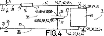
図4は、図3の集積化された実施の回路図を示す。図4は、オーム性抵抗56とキャパシタ37とにより構成されている、フィルタ手段36が低域フィルタを構成していることを明らかに示す。
【0031】
フィルタ手段36のローパス動作のために、手段20によるデータ暗号化及び解読動作の実行によって電源電圧出力端子27、29、31、33と28、30、32、34とに現れる電流ピークパターンが、未発達の強く減衰させられた波形でのみ電圧源端子24、26に生じ、又は、もはやそこに生じさえしない程度までに減衰させられる。その結果、電流ピークパターンは、回路の電源リード21及び22に実際にはもはや生ぜず、そのために電流ピークパターンの調査即ち検出により、手段20における暗号化及び解読のために用いられる鍵についての情報を取り出すことは不可能になる。
【0032】
図5は、別のチップ2を示す。チップ2は、図5にブロックにより線図的に示されているデータキャリヤの回路3を実現する。図5のチップ2は、図2に示されているチップ2に類似して、チップ接点6、10、11と、デジタルセルの列13及び結線ダクト14を有するデジタル部12と、EEPROMにより構成され2つの部分54及びと65により構成されているメモリ15と、アナログ部16とを含む。図5のチップ2は、RAM66と、8つの部分68、69、70、71、72、73、74及び75により構成されているROM67も含む。
【0033】
図5のチップ2は、データの処理に適切であり、ハードウェア技術により実現されているデータ処理手段20も含む。データ処理手段20は、データの暗号化及び解読のための手段20として、ここでも構成されている。
【0034】
その部品が図6に示されている、図5の別のチップ2の回路3は、フィルタ手段36を含む。そのフィルタ手段は、キャパシタ37及びオーム性抵抗56に加えて、電圧源端子24及び26に続く別のフィルタ段76を含む。別のフィルタ段76は、この場合には第2のキャパシタ77と第2のオーム性抵抗78とで構成されている。キャパシタ77及び抵抗78は、接続手段35の接続部79、80及び81を介して相互に接続されているとともに、電圧源端子24及び26に接続されている。接続手段35の接続部58及び56は、第2のキャパシタ77に接続されている。キャパシタ77は、この目的のために2つの接続領域82及び83を含む。接続領域82及び83には接続部80及び81も接続されている。
【0035】
図5のチップ2の回路3に別のフィルタ段76が存在するために、手段20の電源電圧出力端子に生ずる電流ピークパターンの電流ピークの抑制が、図2のチップ2の回路3と比較して改善されている。
【0036】
必要がありかつ有用であれば、フィルタ手段36は、別のフィルタ段を含むこともできることに留意すべきである。
【0037】
本発明は、本発明の説明した2つの実施例に限定されるものではない。それら2つの実施例のおのおのには、データ処理手段20を囲む単一のキャパシタ37のみが設けられている。しかし、必要がありかつ効果的であれば、代わりに2つ又はそれ以上の並列接続されたキャパシタを設けることができる。説明した両方の実施例では、キャパシタ37が組合わされているデータ処理手段20は、データの暗号化及び解読のための手段により構成することもできる。データ処理手段により発生された電流ピークパターンを抑制するために、抑制手段に他のデータ処理手段を組合わせることが有用なこともある。本発明の説明した2つの実施例に合致するデータキャリヤは、接点と送信コイルによる通信のために構成されている。しかし、本発明のデータキャリヤは通信のために代わりに接点のみ又は送信コイルのみを含むことができる。
【図面の簡単な説明】
【図1】 本発明に係る回路の第1の実施例を集積技術によりデータキャリヤにおいて実現するチップを含み、チップカードとして製造された本発明に係るデータキャリヤの第1の実施例の概略平面図である。
【図2】 データの暗号化及び解読のための手段を含み、集積技術によりデータキャリヤのための回路を実現する図1に示されているデータキャリヤのチップの概略平面図である。
【図3】 窓状のキャパシタにより囲まれているデータの暗号化及び解読のための手段を含む図2のチップの一部の断面図である。
【図4】 図3に示されているチップの一部の回路図を示す。
【図5】 集積技術による回路の本発明に係る第2の実施例を実現するデータキャリヤのチップの本発明に係る第2の実施例を、図2に類似して、示す。
【図6】 本発明に係る回路の第2の実施例を含むチップの一部を、図3に類似して、示す。
【符号の説明】
1 データキャリヤ
3 回路
20 データ処理手段
24、26 電圧源端子
27、28、29、30、31、32、33、34 電源電圧出力端子
35 導電性接続手段
36 フィルタ手段
38、39 接続領域
40、41、42、43、44、45、46、47 低オーム性接続部[0001]
BACKGROUND OF THE INVENTION
The present invention is realized in an integrated technology, includes two voltage source terminals capable of supplying a power supply voltage, and is suitable for performing data processing using a characteristic value. Conductive connection for electrically connecting a voltage source terminal to a power supply voltage output terminal, including data processing means including a power supply voltage output terminal interposed to enable supply of power supply voltage to the circuit element of the processing means And a circuit for generating a current peak pattern at a power supply voltage output terminal of the data processing means by data processing by the data processing means, and a pattern configuration of the current peak pattern depending on the processed data and characteristic values. It relates to data carriers.
[0002]
In addition, the present invention is realized in integrated technology, includes two voltage source terminals capable of supplying a power supply voltage, and is suitable for performing data processing while utilizing characteristic values, and is realized in hardware technology. A data processing means including a power supply voltage output terminal interposed to enable supply of a power supply voltage to the circuit element of the data processing means, and a conductive means for conductively connecting the voltage source terminal to the power supply voltage output terminal A data connection means that generates a current peak pattern at a power supply voltage output terminal of the data processing means by data processing by the data processing means, and the pattern configuration of the current peak pattern depends on the processed data and the characteristic value It relates to a circuit for the carrier.
[0003]
[Prior art]
Data carriers of the kind mentioned in the first paragraph and circuits of the kind mentioned in the second paragraph are commercially available and are therefore known. The data processing means in the known data carrier and the known circuit are constituted by encryption / decryption means that allow data to be encrypted and decrypted. During execution of the encryption operation or decryption operation, a current peak pattern is generated at the power supply voltage output terminal of the encryption / decryption means. This current peak pattern represents the meaning of the data processed by the encryption / decryption means and the characteristic values used by the encryption / decryption means, that is, the secret key of those means. In known data carriers and known circuits, each generated current peak pattern not only occurs at the power supply voltage output terminal of the encryption / decryption means but also unfortunately also occurs at the voltage source terminal of the circuit. It is a problem. Therefore, these current peak patterns occur in the power lead of the circuit or data carrier leading to the voltage source terminal. The same current peak pattern that is being generated at the time, during processing of such known data, so as to give the data processing means a given known data for processing in any large number of consecutive times Such an occurrence of each current peak pattern in the power supply lead can be used so that is subject to investigation or detection without exception. While applying a complex but known and available correlation method or comparison method, and while using the detected current peak pattern, during the investigation or detection, the encryption / decryption means The characteristic value used, i.e. the information about the secret key, can be retrieved. Obviously, such decryption of the private key is undesirable. The reason is that the required secret can no longer be guaranteed very reliably.
[0004]
[Problems to be solved by the invention]
The object of the present invention is to avoid the above problems and to provide an improved data carrier and an improved circuit for the data carrier using simple and very few additional means.
[0005]
[Means for Solving the Problems]
To achieve the above object, the data carrier according to the present invention of the type described in the first paragraph can suppress the generation of the current peak pattern generated at the power supply voltage output terminal of the data processing means at the voltage source terminal. A suppression means is further provided.
[0006]
In order to achieve the above object, the circuit according to the present invention of the type described in the second paragraph further suppresses the generation of the current peak pattern generated at the power supply voltage output terminal of the data processing means at the voltage source terminal. It is further characterized by further comprising suppression means capable of
[0007]
By taking the steps according to the invention, the current peak pattern appearing at the power supply voltage output terminal of the data processing means still occurs there for processing of the data by the data processing means, but the invention for the data carrier according to the invention. To the extent that it no longer appears at the voltage source terminal of the circuit according to the present invention or to the extent that it is no longer possible to undesirably investigate or detect the current peak pattern without using the power lead of the circuit according to the present invention. It appears very simply, effectively and reliably that it appears only in a suppressed, undeveloped form. Therefore, the steps according to the present invention indicate that an undesirable conclusion cannot be drawn from the current peak pattern, and therefore that an undesirable determination of a characteristic value such as a secret code, secret key or so-called hash value is impossible. This is a very certain guarantee.
[0008]
The suppression means can be constituted by special data processing means. However, it is particularly advantageous to take the steps disclosed in claims 2 and 9. The reason is that such an implementation is characterized by simplicity and certainty.
[0009]
In the simplest case, the filter means can be constituted by a capacitor, the connection part of the connection means exists between the voltage source terminal and the capacitor, and the ohmic resistance value of the connection part exhibits a low-pass behavior. Is used as a current limiting means configured with a capacitor. However, it has been found to be more advantageous to take the steps disclosed in claims 3 and 10. The reason is that the low-pass behavior of the filter means can be easily adapted to various requirements. If necessary, it has been found to be more advantageous to take further steps disclosed in claims 4 and 11.
[0010]
It should be noted that it is known per se to use a capacitor connected to a voltage source terminal for the data carrier disclosed in the first paragraph or the circuit disclosed in the second paragraph. It is. However, in known data carriers, or known circuits, this capacitor simply constitutes an auxiliary capacitor to bridge the spacing that occurs in the power supply. However, the data carrier according to the present invention or the capacitor in the circuit according to the present invention constitutes a part of the filter means constituting the suppression means for suppressing the current peak pattern.
[0011]
This capacitor realized in integration technology can be, for example, an elongated or L-shaped or U-shaped structure. However, it has been found to be particularly advantageous to take the steps disclosed in claims 5 and 12. Such a structure very effectively attenuates the current peaks that occur during the processing of the data by this data processing means.
[0012]
A structure that conforms to claims 6 and 13 is also advantageous. This is because, for all connections between the two connection areas of the auxiliary capacitor and the power supply voltage output terminal, the shortest possible and thus low ohmic realization is ensured.
[0013]
The steps according to the invention have been found to be particularly advantageous for the data carrier according to the invention disclosed in claim 7 or the circuit according to the invention disclosed in claim 14. The reason is that a very high reliability is ensured regarding the confidentiality of the key for at least one of data encryption and decryption.
[0014]
These and other objects of the present invention will become apparent from and will be elucidated with reference to the embodiments described hereinafter.
[0015]
DETAILED DESCRIPTION OF THE INVENTION
Hereinafter, the present invention will be described in detail with reference to embodiments shown in the drawings. However, the present invention is not limited to the examples.
[0016]
Note particularly that the representations in FIGS. 3 and 5 are highly symbolic. The reason is that it is greatly emphasized to achieve an optimal space-saving arrangement of circuit components for actual implementation on the chip.
[0017]
FIG. 1 shows a data carrier 1 configured as a so-called chip card. The data carrier 1 includes a chip 2. This chip is shown in greater detail in FIG. 2 and constitutes the circuit 3 of the data carrier 1. This circuit is represented diagrammatically in the form of blocks in FIG. The data carrier 1 includes a contact area 4 having a total of eight connecting contacts 5. These contacts are connected to the
[0018]
The circuit 3 of the data carrier 1 is realized by integrated technology and is composed of a plurality of circuit elements represented by blocks in FIG. 2 as already described. Those few circuit elements that are particularly important in this case will be described in detail later.
[0019]
The circuit 3 includes a digital unit 12. The digital part is composed of twelve rows 13 of digital cells (not shown) and wiring ducts 14 arranged between the rows 13. The digital unit 12 constitutes a microprocessor and other digital circuit elements such as a gate and a counter.
[0020]
Other circuit elements to be mentioned include a
[0021]
With regard to the circuit 3, special attention should be given to data processing means 20 that are suitable for processing data using or utilizing characteristic values and that are realized by hardware technology. In this case, the data processing means 20 is configured as means 20 for encrypting and decrypting data. The means 20 includes at least a secret key as a characteristic value used for data encryption and decryption during operation of the
[0022]
FIG. 3 shows a part of the chip 2, ie the circuit 3. The circuit 3 includes data processing means 20, i.e. means 20 for data encryption and decryption. FIG. 3 shows two power leads 21 and 22. During the operation of the data carrier 1 or circuit 3, there is a power supply voltage V between their leads. The first
[0023]
The first voltage source terminal 24 is connected to the first
[0024]
The data encryption / decryption means 20 includes a plurality of power supply voltage output terminals. Of these, power supply
[0025]
With respect to the data encryption and decryption means 20, they are intended to direct the data signal to add the data to be encrypted to the
[0026]
The circuit 3 also includes conductive connection means 35 intended to conductively connect the
[0027]
Due to the fact that the data encryption and decryption means 20 is realized by hardware technology, the behavior of the circuit 3 is that when data is processed by the data processing means 20, ie when data is encrypted and decrypted. In addition, since the data processing is performed, and therefore, the current is supplied to the power supply
[0028]
In the data carrier 1 or its circuit 3, current peak patterns appearing at the power supply
[0029]
Filter means 36 also includes an
[0030]
FIG. 4 shows a circuit diagram of the integrated implementation of FIG. FIG. 4 clearly shows that the filter means 36, which is constituted by an
[0031]
Due to the low-pass operation of the filter means 36, the current peak pattern appearing at the power supply
[0032]
FIG. 5 shows another chip 2. The chip 2 implements a data carrier circuit 3 which is diagrammatically shown by blocks in FIG. 5 is similar to the chip 2 shown in FIG. 2 and is composed of
[0033]
The chip 2 in FIG. 5 also includes data processing means 20 suitable for data processing and realized by hardware technology. The data processing means 20 is also configured here as means 20 for data encryption and decryption.
[0034]
The circuit 3 of another chip 2 of FIG. 5 whose components are shown in FIG. The filter means includes a separate filter stage 76 following the
[0035]
Since there is another filter stage 76 in the circuit 3 of the chip 2 of FIG. 5, the suppression of the current peak of the current peak pattern generated at the power supply voltage output terminal of the
[0036]
It should be noted that the filter means 36 can also include other filter stages if necessary and useful.
[0037]
The present invention is not limited to the two described embodiments of the present invention. In each of these two embodiments, only a
[Brief description of the drawings]
FIG. 1 is a schematic plan view of a first embodiment of a data carrier according to the present invention manufactured as a chip card, including a chip that implements a first embodiment of a circuit according to the present invention in a data carrier by means of integration technology; It is.
2 is a schematic plan view of the chip of the data carrier shown in FIG. 1 which implements a circuit for the data carrier by means of integrated technology, including means for data encryption and decryption.
FIG. 3 is a cross-sectional view of a portion of the chip of FIG. 2 including means for data encryption and decryption surrounded by a window-shaped capacitor.
4 shows a circuit diagram of a part of the chip shown in FIG.
FIG. 5 shows a second embodiment according to the invention of a data carrier chip implementing a second embodiment according to the invention of a circuit according to integrated technology, similar to FIG.
6 shows part of a chip containing a second embodiment of a circuit according to the invention, similar to FIG.
[Explanation of symbols]
1 Data carrier 3
Claims (14)
電源電圧を供給可能な2つの電圧源端子を含み、
特性値を利用しながらデータを処理するために適当であり、ハードウェア技術により実現されるデータ処理手段であって、電源電圧を前記データ処理手段の回路素子に供給可能とするために介在する電源電圧出力端子を含む前記データ処理手段を含み、
前記電圧源端子を前記電源電圧出力端子に導電的に接続するための導電性接続手段を含んでおり、
前記データ処理手段によるデータの処理が前記データ処理手段の前記電源電圧出力端子に電流ピークパターンを出現させ、前記電流ピークパターンのパターン構成が処理されたデータと特性値とに依存する回路を備えたデータキャリヤにおいて、
前記データ処理手段の前記電源電圧出力端子に出現する前記電流ピークパターンの前記電圧源端子における出現を抑制可能な抑制手段がさらに備えられており、
前記抑制手段は、前記データ処理手段を囲む少なくとも一つのキャパシタを備えることを特徴とするデータキャリヤ。Realized by integration technology,
Including two voltage source terminals capable of supplying power supply voltage;
Be suitable for processing data while utilizing a characteristic value, a data processing means implemented in hardware technology, the power supply to mediate supply voltage to be supplied to the circuit elements of the data processing means wherein said data processing means including a voltage output terminal,
The voltage source terminal includes an electrically conductive connection means for connecting the power supply to the voltage output terminal conductively,
The processing of the data by the data processing means causes the appearance of a current peak pattern to the power supply voltage output terminal of the data processing means, the pattern configuration of the current peak pattern is provided with a circuit that depends on the processed data and the characteristic values In the data carrier
The data processing said and appearance in the power supply voltage the voltage source terminal of the current peak pattern appearing on the output terminal is provided with a further possible suppression means suppressing means,
The data carrier , wherein the suppression means comprises at least one capacitor surrounding the data processing means .
前記抑制手段は、前記導電性接続手段に含まれているフィルタ手段により構成され、
前記フィルタ手段は、集積技術により実現され前記データ処理手段の直近に配置されて2つの接続領域を含む前記キャパシタを含み、
前記キャパシタの前記2つの接続領域と、前記データ処理手段の前記電源電圧出力端子とが前記接続手段の低オーム性接続部を介して導電的に接続されていることを特徴とするデータキャリヤ。The data carrier according to claim 1, wherein
The suppressing means comprises a filter means is included in said conductive connecting means,
Said filter means is implemented by an integrated technology include the capacitor including the most recently and arranged in two connection regions of the data processing means,
And said two connection regions of the capacitor, the power supply voltage data carrier, characterized in that the output terminals are conductively connected via low-ohmic connection of said connecting means of said data processing means.
集積技術により実現されて、前記電圧源端子と、前記電圧源端子に導電的に接続されている前記キャパシタの接続領域との間に配置され、前記キャパシタと共に、ローパス挙動を有する前記フィルタ手段を構成する電流制限手段を含むことを特徴とするデータキャリヤ。3. The data carrier of claim 2, wherein the filter means is
Is realized by an integrated technology, construction and the voltage source terminal, is disposed between the connection region of the capacitor which is electrically conductively connected to the voltage source terminal, together with the capacitor, the filter means having a low-pass behavior A data carrier comprising current limiting means.
前記フィルタ手段は、前記キャパシタに加えて、
前記電圧源端子に続く少なくとも1つの別のフィルタ段を含むことを特徴とするデータキャリヤ。The data carrier according to claim 2, wherein
It said filter means, in addition to the capacitor,
Data carrier, characterized in that it comprises at least one further filter stage following the voltage source terminal.
前記キャパシタは、フレーム状構造を有し、前記データ処理手段を完全に囲い込むことを特徴とするデータキャリヤ。The data carrier according to claim 2, wherein
The capacitor, the data carrier, characterized in that has a frame-like structure, Komu completely enclosing the data processing means.
前記データ処理手段は、複数の電源電圧出力端子を含み、
前記キャパシタの2つの接続領域と前記電源電圧出力端子との間に、接続手段の低オーム性接続部であって、前記電源電圧出力端子の数に一致するものが備えられていることを特徴とするデータキャリヤ。The data carrier according to claim 2, wherein
The data processing means includes a plurality of power supply voltage output terminals,
Between the two connection areas and the power supply voltage output terminal of said capacitor, and characterized in that a low-ohmic connection of the connecting means, which corresponds to the number of the power supply voltage output terminal is provided Data carrier.
前記データ処理手段は、データの暗号化と解読の少なくとも一方を行う手段により構成されていることを特徴とするデータキャリヤ。The data carrier according to claim 2, wherein
A data carrier characterized in that the data processing means comprises means for performing at least one of data encryption and decryption.
電源電圧を供給可能な2つの電圧源端子を含み、
特性値を利用しながらデータを処理するために適当であり、ハードウェア技術により実現されるデータ処理手段であって、電源電圧を前記データ処理手段の回路素子に供給可能とするために介在する電源電圧出力端子を含む前記データ処理手段を含み、
前記電圧源端子を前記電源電圧出力端子に導電的に接続するための導電性接続手段を含んでおり、
前記データ処理手段によるデータの処理が前記データ処理手段の前記電源電圧出力端子に電流ピークパターンを出現させ、前記電流ピークパターンのパターン構成が処理されたデータと特性値とに依存する、データキャリヤのための回路において、
前記データ処理手段の前記電源電圧出力端子に出現する前記電流ピークパターンの前記電圧源端子における出現を抑制可能な抑制手段がさらに備えられており、
前記抑制手段は、前記データ処理手段を囲む少なくとも一つのキャパシタを備えることを特徴とする回路。Realized by integration technology,
Including two voltage source terminals capable of supplying power supply voltage;
Be suitable for processing data while utilizing a characteristic value, a data processing means implemented in hardware technology, the power supply to mediate supply voltage to be supplied to the circuit elements of the data processing means wherein said data processing means including a voltage output terminal,
The voltage source terminal includes an electrically conductive connection means for connecting the power supply to the voltage output terminal conductively,
The processing of the data by the data processing means causes the appearance of a current peak pattern to the power supply voltage output terminal of the data processing means, dependent on the data and characteristic values pattern configuration is processed in the current peak pattern, the data carrier In the circuit for
The data processing said and appearance in the power supply voltage the voltage source terminal of the current peak pattern appearing on the output terminal is provided with a further possible suppression means suppressing means,
The circuit, wherein the suppression means includes at least one capacitor surrounding the data processing means .
前記抑制手段は、前記導電性接続手段に含まれているフィルタ手段により構成され、
前記フィルタ手段は、集積技術により実現され前記データ処理手段の直近に配置されて2つの接続領域を含むキャパシタを含み、
前記キャパシタの2つの接続領域と、前記データ処理手段の前記電源電圧出力端子とが前記接続手段の低オーム性接続部を介して導電的に接続されていることを特徴とする回路。The circuit of claim 8, wherein
The suppressing means comprises a filter means is included in said conductive connecting means,
Said filter means is implemented by an integrated technology include capacitor including a most recently and arranged in two connection regions of the data processing means,
And two connection regions of the capacitor, the circuit wherein the power supply voltage output terminal, characterized in that it is electrically conductively connected via a low ohmic connection of said connecting means of said data processing means.
集積技術により実現されて、電圧源端子と、前記電圧源端子に導電的に接続されている前記キャパシタの接続領域との間に配置され、前記キャパシタと共に、ローパス挙動を有する前記フィルタ手段を構成する電流制限手段を含むことを特徴とする回路。 10. The circuit of claim 9, wherein the filter means is
Realized by integrated techniques, is arranged between the voltage source terminal, the connection region of the capacitor which is conductively connected to the voltage source terminal, together with the capacitor, constituting the filter means having a low-pass behavior A circuit comprising current limiting means.
前記フィルタ手段は、前記キャパシタに加えて、
前記電圧源端子に続く少なくとも1つの別のフィルタ段を含むことを特徴とする回路。The circuit of claim 9, wherein
It said filter means, in addition to the capacitor,
A circuit comprising at least one additional filter stage following the voltage source terminal.
前記キャパシタは、フレーム状構造を有し、前記データ処理手段を完全に囲い込むことを特徴とする回路。The circuit of claim 9, wherein
The capacitor has a frame-like structure, circuit, characterized in that Komu completely enclosing the data processing means.
前記データ処理手段は、複数の電源電圧出力端子を含み、
前記キャパシタの2つの接続領域と前記電源電圧出力端子との間に、接続手段の低オーム性接続部であって、前記電源電圧出力端子の数に一致するものが備えられていることを特徴とする回路。The circuit of claim 9, wherein
The data processing means includes a plurality of power supply voltage output terminals,
Between the two connection areas and the power supply voltage output terminal of said capacitor, and characterized in that a low-ohmic connection of the connecting means, which corresponds to the number of the power supply voltage output terminal is provided Circuit.
前記データ処理手段は、データの暗号化と解読の少なくとも一方を行う手段により構成されていることを特徴とする回路。The circuit of claim 9, wherein
The circuit according to claim 1, wherein the data processing means comprises means for performing at least one of data encryption and decryption.
Applications Claiming Priority (3)
| Application Number | Priority Date | Filing Date | Title |
|---|---|---|---|
| EP98890200 | 1998-07-07 | ||
| EP98890200.3 | 1998-07-07 | ||
| PCT/IB1999/001203 WO2000002159A1 (en) | 1998-07-07 | 1999-06-28 | Data carrier provided with data processing means and current peak pattern suppression means |
Publications (2)
| Publication Number | Publication Date |
|---|---|
| JP2002520700A JP2002520700A (en) | 2002-07-09 |
| JP4393707B2 true JP4393707B2 (en) | 2010-01-06 |
Family
ID=8237179
Family Applications (1)
| Application Number | Title | Priority Date | Filing Date |
|---|---|---|---|
| JP2000558484A Expired - Fee Related JP4393707B2 (en) | 1998-07-07 | 1999-06-28 | Data carrier having data processing means and current peak pattern suppressing means |
Country Status (8)
| Country | Link |
|---|---|
| US (1) | US6276609B1 (en) |
| EP (1) | EP1034509B1 (en) |
| JP (1) | JP4393707B2 (en) |
| KR (1) | KR100597421B1 (en) |
| CN (1) | CN1171175C (en) |
| AT (1) | ATE379818T1 (en) |
| DE (1) | DE69937629T2 (en) |
| WO (1) | WO2000002159A1 (en) |
Families Citing this family (10)
| Publication number | Priority date | Publication date | Assignee | Title |
|---|---|---|---|---|
| FR2774492A1 (en) * | 1998-02-04 | 1999-07-30 | Schlumberger Ind Sa | DEVICE WITH INTEGRATED CIRCUIT SECURED BY MITIGATION OF ELECTRIC SIGNATURES |
| US6419159B1 (en) * | 1999-06-14 | 2002-07-16 | Microsoft Corporation | Integrated circuit device with power analysis protection circuitry |
| KR100762530B1 (en) * | 1999-08-31 | 2007-10-01 | 엔엑스피 비 브이 | Data carrier with integrated circuit and transmission coil |
| US7005733B2 (en) * | 1999-12-30 | 2006-02-28 | Koemmerling Oliver | Anti tamper encapsulation for an integrated circuit |
| FR2811790A1 (en) * | 2000-07-11 | 2002-01-18 | Schlumberger Systems & Service | Smart card microcontroller secured against current attacks, uses module between processor and external supply which chaotically encrypts supply current fluctuations |
| DE10245747B4 (en) * | 2002-10-01 | 2005-12-01 | Infineon Technologies Ag | Contactless data carrier |
| US8649820B2 (en) | 2011-11-07 | 2014-02-11 | Blackberry Limited | Universal integrated circuit card apparatus and related methods |
| USD703208S1 (en) | 2012-04-13 | 2014-04-22 | Blackberry Limited | UICC apparatus |
| US8936199B2 (en) | 2012-04-13 | 2015-01-20 | Blackberry Limited | UICC apparatus and related methods |
| USD701864S1 (en) | 2012-04-23 | 2014-04-01 | Blackberry Limited | UICC apparatus |
Family Cites Families (20)
| Publication number | Priority date | Publication date | Assignee | Title |
|---|---|---|---|---|
| FR2401459A1 (en) * | 1977-08-26 | 1979-03-23 | Cii Honeywell Bull | PORTABLE INFORMATION MEDIA EQUIPPED WITH A MICROPROCESSOR AND A PROGRAMMABLE DEAD MEMORY |
| US4577214A (en) * | 1981-05-06 | 1986-03-18 | At&T Bell Laboratories | Low-inductance power/ground distribution in a package for a semiconductor chip |
| DE3130324A1 (en) * | 1981-07-31 | 1983-02-17 | GAO Gesellschaft für Automation und Organisation mbH, 8000 München | CARRIER ELEMENT FOR AN IC COMPONENT |
| JPS62105293A (en) * | 1985-10-31 | 1987-05-15 | Toshiba Corp | Reading/writing device for portable recording medium |
| JPS63118994A (en) * | 1986-11-07 | 1988-05-23 | Seiko Instr & Electronics Ltd | Memory card |
| US4939353A (en) * | 1987-01-22 | 1990-07-03 | Kabushiki Kaisha Toshiba | Processing system for enabling data communication with a self-diagnose device |
| US5687109A (en) * | 1988-05-31 | 1997-11-11 | Micron Technology, Inc. | Integrated circuit module having on-chip surge capacitors |
| US5307309A (en) * | 1988-05-31 | 1994-04-26 | Micron Technology, Inc. | Memory module having on-chip surge capacitors |
| FR2638869B1 (en) * | 1988-11-10 | 1990-12-21 | Sgs Thomson Microelectronics | SECURITY DEVICE AGAINST UNAUTHORIZED DETECTION OF PROTECTED DATA |
| FR2655737B1 (en) * | 1989-12-08 | 1992-06-12 | Sgs Thomson Microelectronics | INTEGRATED CIRCUIT POWER SUPPLY VARIATION DETECTOR. |
| KR100249268B1 (en) * | 1990-11-30 | 2000-03-15 | 가나이 쓰도무 | Semiconductor memory circuit device and method for fabricating same |
| DE4327642C2 (en) * | 1993-05-17 | 1998-09-24 | Anatoli Stobbe | Reader for a detection plate |
| JPH0877318A (en) * | 1994-09-08 | 1996-03-22 | Toshiba Corp | Noncontact information recording medium |
| FR2727225B1 (en) * | 1994-11-22 | 1997-01-24 | Innovatron Ind Sa | PORTABLE OBJECT INCLUDING AN ELECTRONIC CIRCUIT POWERED BY INTERNAL BATTERY AND CONTAINING A DATA MEMORY, PROCESS AND DEVICE FOR EXTERNAL POWERING OF THIS OBJECT AND FOR TRANSFER OF DATA WITH IT |
| US5524556A (en) * | 1995-06-09 | 1996-06-11 | Texas Instruments Incorporated | Induced draft fan control for use with gas furnaces |
| JPH0962808A (en) * | 1995-08-25 | 1997-03-07 | Mitsubishi Electric Corp | Non-contact ic card and non-contact ic card system |
| DE19639033C1 (en) * | 1996-09-23 | 1997-08-07 | Siemens Ag | Copy prevention arrangement for semiconductor chip |
| US5841686A (en) * | 1996-11-22 | 1998-11-24 | Ma Laboratories, Inc. | Dual-bank memory module with shared capacitors and R-C elements integrated into the module substrate |
| FR2774492A1 (en) * | 1998-02-04 | 1999-07-30 | Schlumberger Ind Sa | DEVICE WITH INTEGRATED CIRCUIT SECURED BY MITIGATION OF ELECTRIC SIGNATURES |
| US5998978A (en) * | 1998-06-29 | 1999-12-07 | Motorola, Inc. | Apparatus and method for reducing energy fluctuations in a portable data device |
-
1999
- 1999-06-28 CN CNB998014494A patent/CN1171175C/en not_active Expired - Fee Related
- 1999-06-28 DE DE69937629T patent/DE69937629T2/en not_active Expired - Lifetime
- 1999-06-28 KR KR1020007002363A patent/KR100597421B1/en not_active IP Right Cessation
- 1999-06-28 EP EP99959132A patent/EP1034509B1/en not_active Expired - Lifetime
- 1999-06-28 WO PCT/IB1999/001203 patent/WO2000002159A1/en active IP Right Grant
- 1999-06-28 AT AT99959132T patent/ATE379818T1/en not_active IP Right Cessation
- 1999-06-28 JP JP2000558484A patent/JP4393707B2/en not_active Expired - Fee Related
- 1999-07-06 US US09/348,920 patent/US6276609B1/en not_active Expired - Fee Related
Also Published As
| Publication number | Publication date |
|---|---|
| KR100597421B1 (en) | 2006-07-10 |
| EP1034509A1 (en) | 2000-09-13 |
| US6276609B1 (en) | 2001-08-21 |
| JP2002520700A (en) | 2002-07-09 |
| WO2000002159A1 (en) | 2000-01-13 |
| CN1275224A (en) | 2000-11-29 |
| KR20010023709A (en) | 2001-03-26 |
| ATE379818T1 (en) | 2007-12-15 |
| CN1171175C (en) | 2004-10-13 |
| EP1034509B1 (en) | 2007-11-28 |
| DE69937629D1 (en) | 2008-01-10 |
| DE69937629T2 (en) | 2008-11-13 |
Similar Documents
| Publication | Publication Date | Title |
|---|---|---|
| JP4393707B2 (en) | Data carrier having data processing means and current peak pattern suppressing means | |
| KR100358596B1 (en) | A circuit and method for configuring and registering a cryptographic device | |
| JP3813175B2 (en) | Method for determining an encryption key associated with an integrated circuit | |
| Wollinger et al. | How secure are FPGAs in cryptographic applications? | |
| US6498404B1 (en) | Data carrier with obscured power consumption | |
| US5426323A (en) | Integrated semiconductor circuit with ESD protection | |
| JP2011060303A (en) | Device with integrated circuit made secure by attenuation of electronic signatures | |
| JP2018523290A (en) | Integrated circuit chip protection against physical and / or electrical changes | |
| JPH08321586A (en) | Accumulation semiconductor circuit | |
| US8457302B1 (en) | Access-controlled data storage medium | |
| JP3157715B2 (en) | Semiconductor integrated circuit | |
| JP2003263617A (en) | Method and device for increasing security of circuit against unauthorized access | |
| JPH03142296A (en) | Data carrier | |
| JPH0621356A (en) | Semiconductor device and horizontal register of solid-state image sensing device | |
| US20020088997A1 (en) | Integrated circuit and circuit configuration for supplying power to an integrated circuit | |
| US7602916B1 (en) | Access-protected data carrier | |
| JPH09284119A (en) | Semiconductor integrated circuit device | |
| JP2000076140A (en) | Semiconductor integrated circuit | |
| EP0890956B1 (en) | Semiconductor device having a security circuit for preventing illegal access | |
| JP4034992B2 (en) | Semiconductor device | |
| JP2002526797A (en) | Data processing device for preventing differential current consumption analysis and method of operating this device | |
| JP3063711B2 (en) | Semiconductor integrated circuit | |
| JPS58162065A (en) | Gate prpotecting circuit | |
| JPH05197850A (en) | Data record carrier and electronic device using the carrier | |
| EP1360724A2 (en) | Method of fabricating integrated circuits, providing improved so-called "saw bow" conductive tracks |
Legal Events
| Date | Code | Title | Description |
|---|---|---|---|
| A621 | Written request for application examination |
Free format text: JAPANESE INTERMEDIATE CODE: A621 Effective date: 20060627 |
|
| A711 | Notification of change in applicant |
Free format text: JAPANESE INTERMEDIATE CODE: A711 Effective date: 20080626 |
|
| A131 | Notification of reasons for refusal |
Free format text: JAPANESE INTERMEDIATE CODE: A131 Effective date: 20080916 |
|
| A601 | Written request for extension of time |
Free format text: JAPANESE INTERMEDIATE CODE: A601 Effective date: 20081216 |
|
| A602 | Written permission of extension of time |
Free format text: JAPANESE INTERMEDIATE CODE: A602 Effective date: 20081224 |
|
| A521 | Request for written amendment filed |
Free format text: JAPANESE INTERMEDIATE CODE: A523 Effective date: 20090305 |
|
| TRDD | Decision of grant or rejection written | ||
| A01 | Written decision to grant a patent or to grant a registration (utility model) |
Free format text: JAPANESE INTERMEDIATE CODE: A01 Effective date: 20090915 |
|
| A01 | Written decision to grant a patent or to grant a registration (utility model) |
Free format text: JAPANESE INTERMEDIATE CODE: A01 |
|
| A61 | First payment of annual fees (during grant procedure) |
Free format text: JAPANESE INTERMEDIATE CODE: A61 Effective date: 20091014 |
|
| R150 | Certificate of patent or registration of utility model |
Free format text: JAPANESE INTERMEDIATE CODE: R150 |
|
| FPAY | Renewal fee payment (event date is renewal date of database) |
Free format text: PAYMENT UNTIL: 20121023 Year of fee payment: 3 |
|
| LAPS | Cancellation because of no payment of annual fees |