JP4366732B2 - Method for manufacturing electro-optical device and method for manufacturing drive substrate for electro-optical device - Google Patents
Method for manufacturing electro-optical device and method for manufacturing drive substrate for electro-optical device Download PDFInfo
- Publication number
- JP4366732B2 JP4366732B2 JP27779798A JP27779798A JP4366732B2 JP 4366732 B2 JP4366732 B2 JP 4366732B2 JP 27779798 A JP27779798 A JP 27779798A JP 27779798 A JP27779798 A JP 27779798A JP 4366732 B2 JP4366732 B2 JP 4366732B2
- Authority
- JP
- Japan
- Prior art keywords
- substrate
- single crystal
- tft
- crystal silicon
- film
- Prior art date
- Legal status (The legal status is an assumption and is not a legal conclusion. Google has not performed a legal analysis and makes no representation as to the accuracy of the status listed.)
- Expired - Fee Related
Links
- 239000000758 substrate Substances 0.000 title claims description 230
- 238000000034 method Methods 0.000 title claims description 117
- 238000004519 manufacturing process Methods 0.000 title claims description 82
- 229910021421 monocrystalline silicon Inorganic materials 0.000 claims description 168
- 230000002093 peripheral effect Effects 0.000 claims description 121
- 239000010409 thin film Substances 0.000 claims description 77
- 229910052782 aluminium Inorganic materials 0.000 claims description 59
- XAGFODPZIPBFFR-UHFFFAOYSA-N aluminium Chemical compound [Al] XAGFODPZIPBFFR-UHFFFAOYSA-N 0.000 claims description 59
- 229910052594 sapphire Inorganic materials 0.000 claims description 56
- 239000010980 sapphire Substances 0.000 claims description 56
- 229910052710 silicon Inorganic materials 0.000 claims description 54
- 230000008569 process Effects 0.000 claims description 51
- 239000000463 material Substances 0.000 claims description 48
- XUIMIQQOPSSXEZ-UHFFFAOYSA-N Silicon Chemical compound [Si] XUIMIQQOPSSXEZ-UHFFFAOYSA-N 0.000 claims description 41
- 239000010703 silicon Substances 0.000 claims description 40
- 229910052738 indium Inorganic materials 0.000 claims description 29
- APFVFJFRJDLVQX-UHFFFAOYSA-N indium atom Chemical compound [In] APFVFJFRJDLVQX-UHFFFAOYSA-N 0.000 claims description 29
- GYHNNYVSQQEPJS-UHFFFAOYSA-N Gallium Chemical compound [Ga] GYHNNYVSQQEPJS-UHFFFAOYSA-N 0.000 claims description 28
- 229910052733 gallium Inorganic materials 0.000 claims description 28
- 229910052751 metal Inorganic materials 0.000 claims description 23
- 239000002184 metal Substances 0.000 claims description 23
- 239000000155 melt Substances 0.000 claims description 19
- 238000002844 melting Methods 0.000 claims description 15
- 230000008018 melting Effects 0.000 claims description 15
- 238000001816 cooling Methods 0.000 claims description 10
- 229910052787 antimony Inorganic materials 0.000 claims description 7
- WATWJIUSRGPENY-UHFFFAOYSA-N antimony atom Chemical compound [Sb] WATWJIUSRGPENY-UHFFFAOYSA-N 0.000 claims description 7
- 229910052797 bismuth Inorganic materials 0.000 claims description 7
- JCXGWMGPZLAOME-UHFFFAOYSA-N bismuth atom Chemical compound [Bi] JCXGWMGPZLAOME-UHFFFAOYSA-N 0.000 claims description 7
- 239000011029 spinel Substances 0.000 claims description 5
- 229910052596 spinel Inorganic materials 0.000 claims description 5
- OYLGJCQECKOTOL-UHFFFAOYSA-L barium fluoride Chemical compound [F-].[F-].[Ba+2] OYLGJCQECKOTOL-UHFFFAOYSA-L 0.000 claims description 4
- 229910001632 barium fluoride Inorganic materials 0.000 claims description 4
- FFBGYFUYJVKRNV-UHFFFAOYSA-N boranylidynephosphane Chemical compound P#B FFBGYFUYJVKRNV-UHFFFAOYSA-N 0.000 claims description 4
- WUKWITHWXAAZEY-UHFFFAOYSA-L calcium difluoride Chemical compound [F-].[F-].[Ca+2] WUKWITHWXAAZEY-UHFFFAOYSA-L 0.000 claims description 4
- 229910001634 calcium fluoride Inorganic materials 0.000 claims description 4
- ATJFFYVFTNAWJD-UHFFFAOYSA-N Tin Chemical compound [Sn] ATJFFYVFTNAWJD-UHFFFAOYSA-N 0.000 claims description 3
- HCHKCACWOHOZIP-UHFFFAOYSA-N Zinc Chemical compound [Zn] HCHKCACWOHOZIP-UHFFFAOYSA-N 0.000 claims description 3
- 230000003287 optical effect Effects 0.000 claims description 3
- SIWVEOZUMHYXCS-UHFFFAOYSA-N oxo(oxoyttriooxy)yttrium Chemical compound O=[Y]O[Y]=O SIWVEOZUMHYXCS-UHFFFAOYSA-N 0.000 claims description 3
- RVTZCBVAJQQJTK-UHFFFAOYSA-N oxygen(2-);zirconium(4+) Chemical compound [O-2].[O-2].[Zr+4] RVTZCBVAJQQJTK-UHFFFAOYSA-N 0.000 claims description 3
- FVRNDBHWWSPNOM-UHFFFAOYSA-L strontium fluoride Chemical compound [F-].[F-].[Sr+2] FVRNDBHWWSPNOM-UHFFFAOYSA-L 0.000 claims description 3
- 229910001637 strontium fluoride Inorganic materials 0.000 claims description 3
- 229910052718 tin Inorganic materials 0.000 claims description 3
- 229910052725 zinc Inorganic materials 0.000 claims description 3
- 239000011701 zinc Substances 0.000 claims description 3
- 229910001928 zirconium oxide Inorganic materials 0.000 claims description 3
- 230000008021 deposition Effects 0.000 claims 2
- 239000010408 film Substances 0.000 description 253
- 229920002120 photoresistant polymer Polymers 0.000 description 51
- 108091006146 Channels Proteins 0.000 description 43
- 239000011521 glass Substances 0.000 description 43
- 238000005530 etching Methods 0.000 description 40
- 239000011159 matrix material Substances 0.000 description 39
- 239000012535 impurity Substances 0.000 description 36
- 238000000206 photolithography Methods 0.000 description 35
- 239000004973 liquid crystal related substance Substances 0.000 description 34
- 229910052581 Si3N4 Inorganic materials 0.000 description 33
- HQVNEWCFYHHQES-UHFFFAOYSA-N silicon nitride Chemical compound N12[Si]34N5[Si]62N3[Si]51N64 HQVNEWCFYHHQES-UHFFFAOYSA-N 0.000 description 33
- 230000009977 dual effect Effects 0.000 description 32
- 238000005468 ion implantation Methods 0.000 description 29
- 229910052698 phosphorus Inorganic materials 0.000 description 29
- 239000011574 phosphorus Substances 0.000 description 29
- -1 phosphorus ions Chemical class 0.000 description 29
- 229910021420 polycrystalline silicon Inorganic materials 0.000 description 25
- 238000005268 plasma chemical vapour deposition Methods 0.000 description 21
- OAICVXFJPJFONN-UHFFFAOYSA-N Phosphorus Chemical compound [P] OAICVXFJPJFONN-UHFFFAOYSA-N 0.000 description 20
- 229910021417 amorphous silicon Inorganic materials 0.000 description 19
- 125000004429 atom Chemical group 0.000 description 19
- 229920005989 resin Polymers 0.000 description 19
- 239000011347 resin Substances 0.000 description 19
- 239000013078 crystal Substances 0.000 description 17
- 238000010586 diagram Methods 0.000 description 17
- VYPSYNLAJGMNEJ-UHFFFAOYSA-N Silicium dioxide Chemical compound O=[Si]=O VYPSYNLAJGMNEJ-UHFFFAOYSA-N 0.000 description 16
- 230000015572 biosynthetic process Effects 0.000 description 16
- 239000007772 electrode material Substances 0.000 description 16
- 239000007789 gas Substances 0.000 description 16
- 238000004050 hot filament vapor deposition Methods 0.000 description 16
- 229910052796 boron Inorganic materials 0.000 description 14
- 230000000694 effects Effects 0.000 description 14
- 239000000203 mixture Substances 0.000 description 14
- 238000001994 activation Methods 0.000 description 13
- 229910052785 arsenic Inorganic materials 0.000 description 13
- LIVNPJMFVYWSIS-UHFFFAOYSA-N silicon monoxide Chemical compound [Si-]#[O+] LIVNPJMFVYWSIS-UHFFFAOYSA-N 0.000 description 13
- KFZMGEQAYNKOFK-UHFFFAOYSA-N Isopropanol Chemical compound CC(C)O KFZMGEQAYNKOFK-UHFFFAOYSA-N 0.000 description 12
- 238000009792 diffusion process Methods 0.000 description 12
- 238000010438 heat treatment Methods 0.000 description 11
- VEXZGXHMUGYJMC-UHFFFAOYSA-N Hydrochloric acid Chemical compound Cl VEXZGXHMUGYJMC-UHFFFAOYSA-N 0.000 description 10
- 229910001182 Mo alloy Inorganic materials 0.000 description 10
- ZOKXTWBITQBERF-UHFFFAOYSA-N Molybdenum Chemical compound [Mo] ZOKXTWBITQBERF-UHFFFAOYSA-N 0.000 description 10
- 229910001362 Ta alloys Inorganic materials 0.000 description 10
- 239000011733 molybdenum Substances 0.000 description 10
- 239000004065 semiconductor Substances 0.000 description 10
- 229910004298 SiO 2 Inorganic materials 0.000 description 9
- 150000002500 ions Chemical class 0.000 description 9
- 230000001681 protective effect Effects 0.000 description 9
- 239000005368 silicate glass Substances 0.000 description 9
- 238000004528 spin coating Methods 0.000 description 9
- KRHYYFGTRYWZRS-UHFFFAOYSA-N Fluorane Chemical compound F KRHYYFGTRYWZRS-UHFFFAOYSA-N 0.000 description 8
- 229910045601 alloy Inorganic materials 0.000 description 8
- 239000000956 alloy Substances 0.000 description 8
- 230000000295 complement effect Effects 0.000 description 8
- 230000004888 barrier function Effects 0.000 description 7
- 239000000919 ceramic Substances 0.000 description 7
- 238000005224 laser annealing Methods 0.000 description 7
- 229920000642 polymer Polymers 0.000 description 7
- 239000000243 solution Substances 0.000 description 7
- CPLXHLVBOLITMK-UHFFFAOYSA-N Magnesium oxide Chemical compound [Mg]=O CPLXHLVBOLITMK-UHFFFAOYSA-N 0.000 description 6
- QAOWNCQODCNURD-UHFFFAOYSA-N Sulfuric acid Chemical compound OS(O)(=O)=O QAOWNCQODCNURD-UHFFFAOYSA-N 0.000 description 6
- 238000000137 annealing Methods 0.000 description 6
- 238000007598 dipping method Methods 0.000 description 6
- 229910052750 molybdenum Inorganic materials 0.000 description 6
- 238000000059 patterning Methods 0.000 description 6
- 238000001020 plasma etching Methods 0.000 description 6
- 235000012239 silicon dioxide Nutrition 0.000 description 6
- DGRIPWYWLYDWDO-UHFFFAOYSA-N [Si][In] Chemical compound [Si][In] DGRIPWYWLYDWDO-UHFFFAOYSA-N 0.000 description 5
- RQNWIZPPADIBDY-UHFFFAOYSA-N arsenic atom Chemical compound [As] RQNWIZPPADIBDY-UHFFFAOYSA-N 0.000 description 5
- 230000003647 oxidation Effects 0.000 description 5
- 238000007254 oxidation reaction Methods 0.000 description 5
- 239000007790 solid phase Substances 0.000 description 5
- 238000004544 sputter deposition Methods 0.000 description 5
- ZOXJGFHDIHLPTG-UHFFFAOYSA-N Boron Chemical compound [B] ZOXJGFHDIHLPTG-UHFFFAOYSA-N 0.000 description 4
- 239000004642 Polyimide Substances 0.000 description 4
- NIXOWILDQLNWCW-UHFFFAOYSA-N acrylic acid group Chemical group C(C=C)(=O)O NIXOWILDQLNWCW-UHFFFAOYSA-N 0.000 description 4
- 230000004913 activation Effects 0.000 description 4
- 230000008901 benefit Effects 0.000 description 4
- 239000003795 chemical substances by application Substances 0.000 description 4
- 238000000576 coating method Methods 0.000 description 4
- 230000005684 electric field Effects 0.000 description 4
- 238000007667 floating Methods 0.000 description 4
- 230000001590 oxidative effect Effects 0.000 description 4
- 229920001721 polyimide Polymers 0.000 description 4
- 230000009467 reduction Effects 0.000 description 4
- 229910052814 silicon oxide Inorganic materials 0.000 description 4
- 238000005245 sintering Methods 0.000 description 4
- 229910052715 tantalum Inorganic materials 0.000 description 4
- GUVRBAGPIYLISA-UHFFFAOYSA-N tantalum atom Chemical compound [Ta] GUVRBAGPIYLISA-UHFFFAOYSA-N 0.000 description 4
- XLYOFNOQVPJJNP-UHFFFAOYSA-N water Substances O XLYOFNOQVPJJNP-UHFFFAOYSA-N 0.000 description 4
- 239000011248 coating agent Substances 0.000 description 3
- 229910052681 coesite Inorganic materials 0.000 description 3
- 229910052906 cristobalite Inorganic materials 0.000 description 3
- 229910021419 crystalline silicon Inorganic materials 0.000 description 3
- 238000005401 electroluminescence Methods 0.000 description 3
- 238000005516 engineering process Methods 0.000 description 3
- 230000002708 enhancing effect Effects 0.000 description 3
- 230000005669 field effect Effects 0.000 description 3
- 238000013007 heat curing Methods 0.000 description 3
- 239000003779 heat-resistant material Substances 0.000 description 3
- 239000000395 magnesium oxide Substances 0.000 description 3
- 230000001737 promoting effect Effects 0.000 description 3
- 239000010453 quartz Substances 0.000 description 3
- 238000003847 radiation curing Methods 0.000 description 3
- 239000000565 sealant Substances 0.000 description 3
- 239000000377 silicon dioxide Substances 0.000 description 3
- 239000007787 solid Substances 0.000 description 3
- 125000006850 spacer group Chemical group 0.000 description 3
- 229910052682 stishovite Inorganic materials 0.000 description 3
- 238000002834 transmittance Methods 0.000 description 3
- 229910052905 tridymite Inorganic materials 0.000 description 3
- 229910001316 Ag alloy Inorganic materials 0.000 description 2
- 229910000838 Al alloy Inorganic materials 0.000 description 2
- RYGMFSIKBFXOCR-UHFFFAOYSA-N Copper Chemical compound [Cu] RYGMFSIKBFXOCR-UHFFFAOYSA-N 0.000 description 2
- 229920000742 Cotton Polymers 0.000 description 2
- 239000004988 Nematic liquid crystal Substances 0.000 description 2
- 239000004983 Polymer Dispersed Liquid Crystal Substances 0.000 description 2
- BQCADISMDOOEFD-UHFFFAOYSA-N Silver Chemical compound [Ag] BQCADISMDOOEFD-UHFFFAOYSA-N 0.000 description 2
- 239000002253 acid Substances 0.000 description 2
- 230000009471 action Effects 0.000 description 2
- AZDRQVAHHNSJOQ-UHFFFAOYSA-N alumane Chemical class [AlH3] AZDRQVAHHNSJOQ-UHFFFAOYSA-N 0.000 description 2
- QVGXLLKOCUKJST-UHFFFAOYSA-N atomic oxygen Chemical compound [O] QVGXLLKOCUKJST-UHFFFAOYSA-N 0.000 description 2
- 239000005388 borosilicate glass Substances 0.000 description 2
- 239000003990 capacitor Substances 0.000 description 2
- 230000008859 change Effects 0.000 description 2
- 238000004140 cleaning Methods 0.000 description 2
- 239000000470 constituent Substances 0.000 description 2
- 229910052802 copper Inorganic materials 0.000 description 2
- 239000010949 copper Substances 0.000 description 2
- 229920006332 epoxy adhesive Polymers 0.000 description 2
- 239000005262 ferroelectric liquid crystals (FLCs) Substances 0.000 description 2
- 229910052736 halogen Inorganic materials 0.000 description 2
- 150000002367 halogens Chemical class 0.000 description 2
- BHEPBYXIRTUNPN-UHFFFAOYSA-N hydridophosphorus(.) (triplet) Chemical compound [PH] BHEPBYXIRTUNPN-UHFFFAOYSA-N 0.000 description 2
- 230000001965 increasing effect Effects 0.000 description 2
- 230000002452 interceptive effect Effects 0.000 description 2
- 238000010030 laminating Methods 0.000 description 2
- 239000007788 liquid Substances 0.000 description 2
- 230000007774 longterm Effects 0.000 description 2
- 229910052760 oxygen Inorganic materials 0.000 description 2
- 239000001301 oxygen Substances 0.000 description 2
- 238000010587 phase diagram Methods 0.000 description 2
- KCTAWXVAICEBSD-UHFFFAOYSA-N prop-2-enoyloxy prop-2-eneperoxoate Chemical compound C=CC(=O)OOOC(=O)C=C KCTAWXVAICEBSD-UHFFFAOYSA-N 0.000 description 2
- 229910052709 silver Inorganic materials 0.000 description 2
- 239000004332 silver Substances 0.000 description 2
- 238000010583 slow cooling Methods 0.000 description 2
- JLTRXTDYQLMHGR-UHFFFAOYSA-N trimethylaluminium Chemical compound C[Al](C)C JLTRXTDYQLMHGR-UHFFFAOYSA-N 0.000 description 2
- 238000001771 vacuum deposition Methods 0.000 description 2
- 229910016036 BaF 2 Inorganic materials 0.000 description 1
- 229910004261 CaF 2 Inorganic materials 0.000 description 1
- 108090000699 N-Type Calcium Channels Proteins 0.000 description 1
- 102000004129 N-Type Calcium Channels Human genes 0.000 description 1
- 108010075750 P-Type Calcium Channels Proteins 0.000 description 1
- 229920000297 Rayon Polymers 0.000 description 1
- 229910008313 Si—In Inorganic materials 0.000 description 1
- 239000000853 adhesive Substances 0.000 description 1
- 230000001070 adhesive effect Effects 0.000 description 1
- 239000005354 aluminosilicate glass Substances 0.000 description 1
- DMLAVOWQYNRWNQ-UHFFFAOYSA-N azobenzene Chemical compound C1=CC=CC=C1N=NC1=CC=CC=C1 DMLAVOWQYNRWNQ-UHFFFAOYSA-N 0.000 description 1
- 230000005540 biological transmission Effects 0.000 description 1
- 239000000969 carrier Substances 0.000 description 1
- 150000001875 compounds Chemical class 0.000 description 1
- 239000011231 conductive filler Substances 0.000 description 1
- 210000002858 crystal cell Anatomy 0.000 description 1
- 230000007547 defect Effects 0.000 description 1
- 238000000151 deposition Methods 0.000 description 1
- 230000006866 deterioration Effects 0.000 description 1
- 239000010432 diamond Substances 0.000 description 1
- 229910003460 diamond Inorganic materials 0.000 description 1
- 238000001312 dry etching Methods 0.000 description 1
- 239000000428 dust Substances 0.000 description 1
- 238000010894 electron beam technology Methods 0.000 description 1
- 238000000407 epitaxy Methods 0.000 description 1
- 238000000605 extraction Methods 0.000 description 1
- 239000005357 flat glass Substances 0.000 description 1
- 229910021478 group 5 element Inorganic materials 0.000 description 1
- 229920006015 heat resistant resin Polymers 0.000 description 1
- AMGQUBHHOARCQH-UHFFFAOYSA-N indium;oxotin Chemical compound [In].[Sn]=O AMGQUBHHOARCQH-UHFFFAOYSA-N 0.000 description 1
- 238000002347 injection Methods 0.000 description 1
- 239000007924 injection Substances 0.000 description 1
- 230000001678 irradiating effect Effects 0.000 description 1
- 239000006062 low-transmittance glass Substances 0.000 description 1
- 239000012528 membrane Substances 0.000 description 1
- 150000002894 organic compounds Chemical class 0.000 description 1
- 239000012071 phase Substances 0.000 description 1
- 125000004437 phosphorous atom Chemical group 0.000 description 1
- 238000001259 photo etching Methods 0.000 description 1
- 230000000704 physical effect Effects 0.000 description 1
- 239000000049 pigment Substances 0.000 description 1
- 229920003229 poly(methyl methacrylate) Polymers 0.000 description 1
- 238000012805 post-processing Methods 0.000 description 1
- 230000003405 preventing effect Effects 0.000 description 1
- 238000010791 quenching Methods 0.000 description 1
- 230000000171 quenching effect Effects 0.000 description 1
- 239000002964 rayon Substances 0.000 description 1
- 230000004044 response Effects 0.000 description 1
- 238000007789 sealing Methods 0.000 description 1
- 238000009751 slip forming Methods 0.000 description 1
- 229910001415 sodium ion Inorganic materials 0.000 description 1
- 238000000992 sputter etching Methods 0.000 description 1
- 238000003860 storage Methods 0.000 description 1
- 239000000126 substance Substances 0.000 description 1
- 230000001629 suppression Effects 0.000 description 1
- 230000001360 synchronised effect Effects 0.000 description 1
Images


Classifications
-
- H—ELECTRICITY
- H01—ELECTRIC ELEMENTS
- H01L—SEMICONDUCTOR DEVICES NOT COVERED BY CLASS H10
- H01L27/00—Devices consisting of a plurality of semiconductor or other solid-state components formed in or on a common substrate
- H01L27/02—Devices consisting of a plurality of semiconductor or other solid-state components formed in or on a common substrate including semiconductor components specially adapted for rectifying, oscillating, amplifying or switching and having potential barriers; including integrated passive circuit elements having potential barriers
- H01L27/12—Devices consisting of a plurality of semiconductor or other solid-state components formed in or on a common substrate including semiconductor components specially adapted for rectifying, oscillating, amplifying or switching and having potential barriers; including integrated passive circuit elements having potential barriers the substrate being other than a semiconductor body, e.g. an insulating body
- H01L27/1214—Devices consisting of a plurality of semiconductor or other solid-state components formed in or on a common substrate including semiconductor components specially adapted for rectifying, oscillating, amplifying or switching and having potential barriers; including integrated passive circuit elements having potential barriers the substrate being other than a semiconductor body, e.g. an insulating body comprising a plurality of TFTs formed on a non-semiconducting substrate, e.g. driving circuits for AMLCDs
- H01L27/1259—Multistep manufacturing methods
- H01L27/127—Multistep manufacturing methods with a particular formation, treatment or patterning of the active layer specially adapted to the circuit arrangement
-
- G—PHYSICS
- G02—OPTICS
- G02F—OPTICAL DEVICES OR ARRANGEMENTS FOR THE CONTROL OF LIGHT BY MODIFICATION OF THE OPTICAL PROPERTIES OF THE MEDIA OF THE ELEMENTS INVOLVED THEREIN; NON-LINEAR OPTICS; FREQUENCY-CHANGING OF LIGHT; OPTICAL LOGIC ELEMENTS; OPTICAL ANALOGUE/DIGITAL CONVERTERS
- G02F1/00—Devices or arrangements for the control of the intensity, colour, phase, polarisation or direction of light arriving from an independent light source, e.g. switching, gating or modulating; Non-linear optics
- G02F1/01—Devices or arrangements for the control of the intensity, colour, phase, polarisation or direction of light arriving from an independent light source, e.g. switching, gating or modulating; Non-linear optics for the control of the intensity, phase, polarisation or colour
- G02F1/13—Devices or arrangements for the control of the intensity, colour, phase, polarisation or direction of light arriving from an independent light source, e.g. switching, gating or modulating; Non-linear optics for the control of the intensity, phase, polarisation or colour based on liquid crystals, e.g. single liquid crystal display cells
- G02F1/133—Constructional arrangements; Operation of liquid crystal cells; Circuit arrangements
- G02F1/1333—Constructional arrangements; Manufacturing methods
- G02F1/1345—Conductors connecting electrodes to cell terminals
- G02F1/13454—Drivers integrated on the active matrix substrate
-
- H—ELECTRICITY
- H01—ELECTRIC ELEMENTS
- H01L—SEMICONDUCTOR DEVICES NOT COVERED BY CLASS H10
- H01L27/00—Devices consisting of a plurality of semiconductor or other solid-state components formed in or on a common substrate
- H01L27/02—Devices consisting of a plurality of semiconductor or other solid-state components formed in or on a common substrate including semiconductor components specially adapted for rectifying, oscillating, amplifying or switching and having potential barriers; including integrated passive circuit elements having potential barriers
- H01L27/12—Devices consisting of a plurality of semiconductor or other solid-state components formed in or on a common substrate including semiconductor components specially adapted for rectifying, oscillating, amplifying or switching and having potential barriers; including integrated passive circuit elements having potential barriers the substrate being other than a semiconductor body, e.g. an insulating body
- H01L27/1214—Devices consisting of a plurality of semiconductor or other solid-state components formed in or on a common substrate including semiconductor components specially adapted for rectifying, oscillating, amplifying or switching and having potential barriers; including integrated passive circuit elements having potential barriers the substrate being other than a semiconductor body, e.g. an insulating body comprising a plurality of TFTs formed on a non-semiconducting substrate, e.g. driving circuits for AMLCDs
- H01L27/1259—Multistep manufacturing methods
- H01L27/1296—Multistep manufacturing methods adapted to increase the uniformity of device parameters
Landscapes
- Engineering & Computer Science (AREA)
- Physics & Mathematics (AREA)
- Power Engineering (AREA)
- General Physics & Mathematics (AREA)
- Condensed Matter Physics & Semiconductors (AREA)
- Computer Hardware Design (AREA)
- Microelectronics & Electronic Packaging (AREA)
- Manufacturing & Machinery (AREA)
- Nonlinear Science (AREA)
- Chemical & Material Sciences (AREA)
- Crystallography & Structural Chemistry (AREA)
- Optics & Photonics (AREA)
- Mathematical Physics (AREA)
- Liquid Crystal (AREA)
- Thin Film Transistor (AREA)
- Recrystallisation Techniques (AREA)
- Vessels, Lead-In Wires, Accessory Apparatuses For Cathode-Ray Tubes (AREA)
- Cathode-Ray Tubes And Fluorescent Screens For Display (AREA)
Description
【0001】
【発明の属する技術分野】
本発明は、電気光学装置の製造方法及び電気光学装置用の駆動基板の製造方法に関し、特に絶縁基板上にヘテロエピタキシャル成長させた単結晶シリコン層を能動領域に用いるトップゲート型の薄膜絶縁ゲート型電界効果トランジスタ(以降、トップゲート型MOSTFTと呼ぶ。尚、トップゲート型にはスタガー型とコプラナー型が含まれる。)と受動領域を有する液晶表示装置などに好適な方法に関するものである。
【0002】
【従来の技術】
アクティブマトリクス型の液晶表示装置として、アモルファスシリコンをTFTに用いた表示部と外付け駆動回路用ICとを有するものや、固相成長法による多結晶シリコンをTFTに用いた表示部と駆動回路との一体型(特開平6−242433号公報)、エキシマレーザーアニールを行った多結晶シリコンをTFTに用いた表示部と駆動回路との一体型(特開平7−131030号公報)などが知られている。
【0003】
【発明が解決しようとする課題】
しかし、上記した従来のアモルファスシリコンTFTは、生産性は良いが、電子移動度は0.5〜1.0cm2 /v・sec前後と低いために、pチャンネルのMOSTFT(以降、pMOSTFTと呼ぶ。)を作ることができない。従って、pMOSTFTを用いた周辺駆動部を表示部と同じガラス基板上に形成できないため、ドライバICは外付けとなり、TAB方式等により実装されるので、コストダウンが難しい。また、このために、高精細化には限界がある。更に、電子移動度は0.5〜1.0cm2 /v・sec前後と低いので、十分なオン電流がとれず、表示部に用いた場合、トランジスタサイズが必然的に大きくなり、画素の高開口率に不利である。
【0004】
また、上記した従来の多結晶シリコンTFTの電子移動度は70〜100cm2 /v・secで高精細化にも対応できるので、最近は駆動回路一体型の多結晶シリコンTFTを用いたLCD(液晶表示装置)が注目されている。しかし、15インチ以上の大型LCDの場合は、多結晶シリコンの電子移動度は70〜100cm2 /v・secであるため、駆動能力が不足し、結局、外付けの駆動回路用ICが必要となっている。
【0005】
また、固相成長法により成膜された多結晶シリコンを用いるTFTでは、600℃以上で十数時間のアニールと、約1000℃の熱酸化によるゲートSiO2 の形成が必要なために、半導体製造装置を採用せざるを得ない。そのために、ウエーハサイズ8〜12インチφが限界であり、高耐熱性で高価な石英ガラスの採用が余儀なくされ、コストダウンが難しい。従って、EVFやデータ/AVプロジェクタ用途に限定されている。
【0006】
更に、上記した従来のエキシマレーザーアニールによる多結晶シリコンTFTでは、エキシマレーザー出力の安定性、生産性、大型化による装置価格の上昇、歩留/品質低下等の問題が山積している。
【0007】
特に、1m角等の大型ガラス基板になると、前記の問題が拡大し、ますます性能/品質向上とコストダウンが難しくなる。
【0008】
本発明の目的は、特に周辺駆動回路部において、高い電子/正孔移動度の単結晶シリコン層を比較的低温でかつ均一に成膜して、高性能ドライバ内蔵のアクティブマトリクス基板と、これを用いた表示用薄膜半導体装置等の電気光学装置の製造を可能とし、高いスイッチング特性と低リーク電流を有するLDD構造(Lightly doped drain 構造) のnチャンネルのMOSTFT(以降、nMOSTFTと呼ぶ。)又はpMOSTFT又は高い駆動能力の相補型薄膜絶縁ゲート電界効果トランジスタ(以降、cMOSTFTと呼ぶ。)の表示部と、このcMOSTFT又はnMOSTFT又はpMOSTFT、或いはこれらの混在からなる周辺駆動回路とを一体化した構成を可能とし、高画質、高精細、狭額縁、高効率、大画面の表示パネルを実現することができ、しかも歪点が比較的低い大型のガラス基板であっても使用でき、生産性が高く、高価な製造設備が不要であってコストダウンが可能となり、更に、しきい値調整が容易であって低抵抗化による高速動作と大画面化を可能にすることにある。
【0009】
【課題を解決するための手段】
即ち、本発明は、画素電極(例えばマトリクス状に配列された複数の画素電極:以下、同様)が配された表示部と、この表示部の周辺に配された周辺駆動回路部とを第1の基板(即ち、駆動用の基板:以下、同様)上に有し、この第1の基板と第2の基板(即ち、対向基板:以下、同様)との間に液晶などの所定の光学材料を介在させてなる電気光学装置、及びこの電気光学装置用の駆動基板のそれぞれの製造方法において、
前記第1の基板の前記一方の面上に、単結晶シリコンと格子整合の良い後述の物質層
を形成する工程と、
この物質層を含む前記第1の基板上にシリコンを含有する後述の低融点金属の溶融液
層を形成する工程と、
次いで冷却処理(望ましくは徐冷処理)によって前記溶融液層の前記シリコンを前記
物質層をシードとしてヘテロエピタキシャル成長させ、単結晶シリコン層を析出させる
工程と、
この単結晶シリコン層に所定の処理を施して能動素子及び受動素子のうちの少なくと
も能動素子を形成する工程(例えば前記単結晶シリコン層の析出後に、この単結晶シリ
コン層に所定の処理を施してチャンネル領域、ソース領域及びドレイン領域を形成する
工程と、前記チャンネル領域の上部にゲート絶縁膜及びゲート電極からなるゲート部、
更にはソース及びドレイン電極を形成して、前記周辺駆動回路部の少なくとも一部を構
成するトップゲート型の第1の薄膜トランジスタ(特にMOSTFT:以下、同様)を
能動素子として形成する工程とを行う工程、又は、抵抗、キャパシタンス、インダクタ
ンス等の受動素子を形成する工程)と
を有することを特徴とする、電気光学装置、及びこの電気光学装置用の駆動基板の製造方法に係るものである。なお、本発明において、上記能動素子は薄膜トランジスタやその他のダイオード等の素子を含む概念であり、上記受動素子は抵抗などを含む概念である(以下、同様)。その代表例としての薄膜トランジスタとは、電界効果トランジスタ(FET)(これにはMOS型と接合型があるが、いずれでもよい。)とバイポーラトランジスタとがあるが、本発明はいずれのトランジスタにも適用できる(以下、同様)。また、上記受動素子は抵抗、インダクタンス、キャパシタンス等を含む概念であり、例えばシリコンナイトライド(以後SiNと呼ぶ。)等の高誘電体膜を低抵抗化した前記単結晶シリコン層(電極)で挟み込んで形成したキャパシタンスがある。
【0010】
本発明によれば、特に単結晶シリコンと格子整合の良い上記物質層(例えば結晶性サファイア膜)をシードにして、シリコン等を溶解した低融点金属の溶融液から、ヘテロエピタキシャル成長で単結晶シリコン薄膜などの単結晶半導体薄膜を形成し、このエピタキシャル成長層をアクティブマトリクス基板などの駆動基板の周辺駆動回路のトップゲート型MOSTFTや表示部−周辺駆動回路一体型のLCDなどの電気光学装置の周辺駆動回路のトップゲート型MOSTFTなどの能動素子や、抵抗、インダクタンス、キャパシタンス等の受動素子のうちの少なくとも能動素子に用いているので、次の(A)〜(G)に示す顕著な作用効果を得ることができる。
【0011】
(A)単結晶シリコンと格子整合の良い物質層(例えば結晶性サファイア膜)を基板上に形成し、その物質層をシードとしてヘテロエピタキシャル成長させることにより、540cm2 /v・sec以上の高い電子移動度の単結晶シリコン薄膜の如き単結晶半導体層が得られるので、高性能ドライバ内蔵の表示用薄膜半導体装置などの電気光学装置の製造が可能となる。
【0012】
(B)特にこの単結晶シリコン層は、従来のアモルファスシリコン層や多結晶シリコン層に比べて、単結晶シリコン基板並の高い電子及び正孔移動度を示すので、これによる単結晶シリコントップゲート型MOSTFTは、高いスイッチング特性〔望ましくは更に、電界強度を緩和して低リーク電流化するLDD(Lightly doped drain) 構造〕を有するnMOS又はpMOSTFT又はcMOSTFTからなる表示部と、高い駆動能力のcMOS、又はnMOS、pMOSTFT又はこれらの混在からなる周辺駆動回路部とを一体化した構成が可能となり、高画質、高精細、狭額縁、高効率、大画面の表示パネルが実現する。特に、多結晶シリコンではLCD用TFTとして、高い正孔移動度のpMOSTFTは形成し難いが、本発明による単結晶シリコン層は正孔でも十分に高い移動度を示すため、電子と正孔をそれぞれ単独でも、或いは双方を組み合せて駆動する周辺駆動回路を作製でき、これをnMOS又はpMOS又はcMOSのLDD構造の表示部用TFTと一体化したパネルを実現できる。また、小型〜中型パネルの場合には、周辺の一対の垂直駆動回路の一方を省略できる可能性がある。
【0013】
(C)そして、上記した物質層をヘテロエピタキシャル成長のシードとして用い、かつこの物質層上において、上記した低融点金属の溶融液を低温(例えば350℃)で調製し、それより少し高いだけの温度に加熱した基板上に塗布などの方法で形成できるから、比較的低温(例えば300〜400℃)でシリコン単結晶膜を均一に形成することができる。
【0014】
(D)固相成長法の場合のような中温で長時間(約600℃、十数時間)のアニールや、エキシマレーザーアニールが不要となるから、生産性が高く、高価な製造設備が不要でコストダウンが可能となる。
【0015】
(E)このヘテロエピタキシャル成長では、結晶性サファイア膜等の物質層の結晶性、溶融液の組成比、溶融液温度、基板の加熱温度、冷却速度等の調整により広範囲のP型不純物濃度と高移動度の単結晶シリコン層が容易に得られるので、Vth(しきい値)調整が容易であり、低抵抗化による高速動作が可能である。
【0016】
(F)また、シリコン含有低融点金属溶融液層に、3族又は5族の不純物元素(ボロン、リン、アンチモン、ひ素、ビスマス、アルミニウムなど)を別途適量ドープしておけば、ヘテロエピタキシャル成長による単結晶シリコン薄膜の不純物種及び/又はその濃度、即ちP型/N型等の導電型及び/又はキャリア濃度を任意に制御することができる。
【0017】
(G)結晶性サファイア膜などの上記物質層は、様々な原子の拡散バリアになるため、ガラス基板からの不純物の拡散を抑制することができる。
【0018】
【発明の実施の形態】
本発明においては、前記単結晶シリコン層に所定の処理を施してチャンネル領域、ソース領域及びドレイン領域とし、前記チャンネル領域の上部にゲート部を有するトップゲート型の第1の薄膜トランジスタが前記周辺駆動回路部の少なくとも一部を構成するのがよい。
【0019】
そして、前記第1の基板として絶縁基板が用いられ、前記物質層がサファイア(Al2 O3 )、スピネル構造体(例えばMgO・Al2 O3 )、フッ化カルシウム(CaF2 )、フッ化ストロンチウム(SrF2 )、フッ化バリウム(BaF2 )、リン化ボロン(BP)、酸化イットリウム((Y2 O3 )m )及び酸化ジルコニウム((ZrO2 )1 -m)等からなる群より選ばれた物質で形成されているのがよい。
【0020】
このような物質層上において、シリコンを例えば2.0重量%〜0.005重量%、例えば1重量%含有する低融点金属の溶融液を加熱された絶縁基板に塗布し、所定時間(数分〜数10分)保持した後、前記冷却処理を行うのがよい。これによって、厚さ数μm〜0.005μm、例えば1μmの単結晶シリコン膜を得ることができる。
【0021】
また、前記基板として絶縁基板、例えばガラス基板、耐熱性有機基板を使用し、前記低融点金属としてインジウム、ガリウム、スズ、ビスマス、鉛、亜鉛、アンチモン及びアルミニウムからなる群より選ばれた少なくとも1種を使用することができる。
【0022】
この場合、前記低融点金属としてインジウムを使用するときには前記溶融液を850〜1100℃、望ましくは900〜950℃に加熱された前記絶縁基板に塗布し、前記低融点金属としてインジウム・ガリウム又はガリウムを使用するときには前記溶融液を300〜1100℃、望ましくは350〜600℃又は400〜1100℃、望ましくは420〜600℃に加熱された前記絶縁基板に塗布することができる。基板の加熱は、電気炉やランプ等を用いて基板全体を均一に加熱する方法の他、光レーザー、電子ビーム等によって、所定の場所のみを局部的に加熱する方法も可能である。
【0023】
このようにシリコンを含有する低融点金属は、図10に示す状態図から明らかなように、低融点金属の割合に応じて融点が低下する。インジウムを用いるときには、シリコンを含有(例えば1重量%含有)するインジウム溶融液層を850〜1100℃の基板温度で形成するのは、1000℃程度までは基板として石英板ガラスを使用でき、1100℃〜850℃まではそれよりも耐熱性が低いガラス、例えば結晶化ガラスでも使用できることになる。ガリウムを用いるときにも、上記と同様の理由から、シリコンを含有(例えば1重量%含有)するガリウム溶融液層を400〜1100℃の基板温度で形成することができる。
【0024】
後者の場合(インジウム・ガリウム・シリコン又はガリウム・シリコンの場合)、基板として、比較的歪点の低いガラス基板や耐熱性有機基板を用い得るので、大型ガラス基板(例えば1m2 以上)上に半導体結晶層を作成することが可能であるが、このような基板は、安価で、薄板化が容易であり、長尺ロール化されたガラス板を作製できる。これを用いて、長尺ロール化ガラス板や耐熱性有機基板上に、上記手法により、ヘテロエピタキシャル成長による単結晶シリコン薄膜を連続して又は非連続に作製することができる。
【0025】
上記の溶融液塗布式では一定時間(数分〜数十分)保持した後に徐冷するが、この他にも、ガラス基板を上記溶液に浸して、一定時間(数分〜数十分)保持した後、徐々に引き上げるディッピング方式や、溶融液中又は表面を適切な速度で移動させて徐冷するフローティング方式でもよい。溶融液の組成、温度、引き上げ速度によって、ヘテロエピタキシャル成長層の厚さやキャリア不純物濃度を制御することができる。塗布式、ディッピング方式、フローティング方式等は、基板を連続又は断続送りして処理できるため、量産性も向上する。
【0026】
上記のように、歪点が低いガラスの上層へは、このガラス内部から、その構成元素が拡散し易いので、これを抑える目的で、拡散バリア層の薄膜(例えばシリコンナイトライド(SiN):厚さ50〜200nm程度)などの膜を形成するのがよい。従ってこの場合、拡散バリア層上に前記多結晶又はアモルファスシリコン層又はシリコン含有の低融点金属層を形成する。
【0027】
上記したシリコンを溶かした低融点金属から、徐冷によって、上記物質層をシードとしてヘテロエピタキシャル成長により前記単結晶シリコン層を析出させた後に、この上の前記低融点金属の層を塩酸などで溶解除去し、しかる後に前記単結晶シリコン層に所定の処理を施して能動素子と受動素子を作製することができる。
【0028】
このように、徐冷後に単結晶シリコン層の上に析出したインジウムなどの低融点金属薄膜は塩酸等を用いて溶解除去するが、インジウム等はシリコン層中に微量(1016atoms/cc程度)しか残留しないよう作成できるので、作成直後はP型の単結晶シリコン薄膜の半導体が作成される。従って、これはnMOSTFTの作製にとって都合が良い。しかし、適量のリン原子などのN型不純物を全面又は選択的にイオン注入することによって、全面又は選択的にN型の単結晶シリコン薄膜を作成することができるので、pMOSTFTも作成することができる。このため、cMOSTFTも作成できることになる。多結晶又はアモルファスシリコン又はシリコン含有低融点金属層の成膜時に、溶解度が大きい3族又は5族の不純物元素(ボロン、リン、アンチモン、ひ素、ビスマスなど)を別途適量ドープしておけば、成長するシリコンエピタキシャル成長層の不純物種及び/又はその濃度、即ち、P型/N型及び/又はキャリア濃度を任意に制御することができる。
【0029】
このように、基板上にヘテロエピタキシャル成長した前記単結晶シリコン層を周辺駆動回路の少なくとも一部を構成するトップゲート型MOSTFTのチャンネル領域、ソース領域及びドレイン領域に適用し、これら各領域の不純物種及び/又はその濃度を制御することができる。
【0030】
前記周辺駆動回路部及び前記表示部の薄膜トランジスタがnチャンネル型、pチャンネル型又は相補型の絶縁ゲート電界効果トランジスタを構成し、例えば相補型とnチャンネル型との組、相補型とpチャンネル型との組、又は相補型とnチャンネル型とpチャンネル型との組からなっていてよい。また、前記周辺駆動回路部及び/又は前記表示部の薄膜トランジスタの少なくとも一部がLDD(Lightly doped drain)構造を有しているのがよい。なお、LDD構造は、ゲート−ドレイン間のみならず、ゲート−ソース間にも、又はゲート−ソース間及びゲート−ドレイン間の両方に設けてもよい(これをダブルLDDと呼ぶ)。
【0031】
特に、前記MOSTFTは表示部では、nMOS又はpMOS又はcMOSのLDD型TFTを構成し、また周辺駆動回路部では、cMOS又はnMOS又はpMOSTFT又はこれらの混在を構成しているのがよい。
【0032】
本発明においては、前記基板及び/又はその上の膜に段差を設け、この段差を断面において底面に対し側面が直角状若しくは下端側へ望ましくは90°以下の底角をなすように傾斜状となるような凹部として、絶縁基板又はその上のSiNなどの膜(或いはこれらの双方)に形成するのがよい。この段差は前記単結晶シリコン層のヘテロエピタキシャル成長時のシードとなり、単結晶シリコン膜の結晶性を高め、その成長を促進させる作用があると思われる。この段差は、前記能動素子、例えば薄膜トランジスタの前記チャンネル領域、前記ソース領域及び前記ドレイン領域で形成される素子領域の少なくとも一辺に沿って形成するのがよい。また、前記受動素子、例えば抵抗が形成される素子領域の少なくとも一辺に沿って形成されているのがよい。
【0033】
この場合、前記基板としての絶縁基板上に、前記ヘテロエピタキシャル成長のシードとなり、単結晶シリコン膜の結晶性を高め、その成長を促進する作用がある上記した如き所定形状の段差を所定位置に形成し、この段差を含む前記絶縁基板上に前記物質層を形成することができる。
【0034】
或いは、前記物質層に上記と同様な所定形状の段差を形成し、この段差を含む前記物質層上に前記単結晶シリコン層を形成することができる。
【0035】
これらの場合、上記物質層に加え、上記段差もヘテロエピタキシャル成長のシードとして作用するため、より結晶性の高い単結晶シリコン層を形成でき、その成長を促進することができる。
【0036】
前記MOSTFTの如き第1の薄膜トランジスタを前記段差による基板凹部内に設けてよいが、凹部外の凹部付近、或いはこれらの双方において基板上に設けてもよい。前記段差はリアクティブイオンエッチングなどのドライエッチングによって形成してよい。
【0037】
この場合、前記第1の基板の一方の面上に上記の段差を形成し、この段差を含む前記基板上に結晶性サファイア膜と単結晶、多結晶又はアモルファスシリコン層を形成し、前記第2の薄膜トランジスタを、前記単結晶、多結晶又はアモルファスシリコン層をチャンネル領域、ソース領域及びドレイン領域とし、前記チャンネル領域の上部及び/又は下部にゲート部を有するトップゲート型、ボトムゲート型又はデュアルゲート型としてよい。
【0038】
この場合も、断面において底面に対し側面が直角状若しくは下端側へ望ましくは90°以下の底角をなすように傾斜状となるような凹部として上記と同様の前記段差を形成し、この段差を前記単結晶シリコン層のヘテロエピタキシャル成長時のシードとし、成長速度の向上及び結晶性を高める役割をさせる。
【0039】
前記第2の薄膜トランジスタは、前記第1の基板及び/又はその上の膜に形成した前記段差による基板凹部内及び/又は外に設け、前記第1の薄膜トランジスタと同様にヘテロエピタキシャル成長による単結晶シリコン層を用いて、そのソース、ドレイン、チャンネルの各領域を形成してよい。
【0040】
この第2の薄膜トランジスタでも、上記したと同様、前記単結晶、多結晶又はアモルファスシリコン層の3族又は5族の不純物種及び/又はその濃度を制御したり、前記段差を、前記第2の薄膜トランジスタの前記チャンネル領域、前記ソース領域及び前記ドレイン領域で形成される素子領域の少なくとも一辺に沿って形成してよい。また、前記単結晶、多結晶又はアモルファスシリコン層下のゲート電極をその側端部にて台形状にするのがよい。前記第1の基板と前記単結晶、多結晶又はアモルファスシリコン層との間に拡散バリア層を設けてよい。
【0041】
前記第1及び/又は第2の薄膜トランジスタのソース又はドレイン電極を前記段差を含む領域上に形成するのがよい。
【0042】
前記第1の薄膜トランジスタを、チャンネル領域の上部及び/又は下部にゲート部を有するトップゲート型、ボトムゲート型又はデュアルゲート型の中から選ばれた少なくともトップゲート型とし、かつ、表示部において画素電極をスイッチングするスイッチング素子を、前記トップゲート型、前記ボトムゲート型又は前記デュアルゲート型の第2の薄膜トランジスタとしてよい。
【0043】
この場合、チャンネル領域の下部に設けられたゲート電極を耐熱性材料で形成したり、前記第2の薄膜トランジスタの上部ゲート電極と前記第1の薄膜トランジスタのゲート電極とを共通の材料で形成してよい。
【0044】
前記周辺駆動回路部において、前記第1の薄膜トランジスタ以外に、多結晶又はアモルファスシリコン層をチャンネル領域とし、このチャンネル領域の上部及び/又は下部にゲート部を有するトップゲート型、ボトムゲート型又はデュアルゲート型の薄膜トランジスタ、或いは前記単結晶シリコン層又は多結晶シリコン層又はアモルファスシリコン層を用いたダイオード、抵抗、キャパシタンス、インダクタンス素子などを設けてよい。
【0045】
前記周辺駆動回路部及び/又は前記表示部の薄膜トランジスタを、シングルゲート又はマルチゲートに構成してよい。
【0046】
前記周辺駆動回路部及び/又は前記表示部のn又はpチャンネル型の薄膜トランジスタがデュアルゲート型であるときには、上部又は下部ゲート電極を電気的にオープンとするか或いは任意の負電圧(nチャンネル型の場合)又は正電圧(pチャンネル型の場合)を印加し、ボトムゲート型又はトップゲート型の薄膜トランジスタとして動作するのがよい。
【0047】
前記周辺駆動回路部の薄膜トランジスタをnチャンネル型、pチャンネル型又は相補型の前記第1の薄膜トランジスタとし、前記表示部の薄膜トランジスタを、単結晶シリコン層をチャンネル領域とするときはnチャンネル型、pチャンネル型又は相補型であり、多結晶シリコン層をチャンネル領域とするときにはnチャンネル型、pチャンネル型又は相補型とし、アモルファスシリコン層をチャンネル領域とするときにはnチャンネル型、pチャンネル型又は相補型としてよい。
【0048】
本発明において、前記単結晶シリコン層の成長後、この単結晶シリコン層上にゲート絶縁膜とゲート電極とからなる上部ゲート部を形成し、この上部ゲート部をマスクとして前記単結晶シリコン層に3族又は5族の不純物元素を導入して前記チャンネル領域、前記ソース領域及び前記ドレイン領域を形成してよい。
【0049】
また、前記第2の薄膜トランジスタがボトムゲート型又はデュアルゲート型であるときは、前記チャンネル領域の下部に耐熱性材料からなる下部ゲート電極を設け、このゲート電極上にゲート絶縁膜を形成して下部ゲート部を形成した後、前記段差の形成工程を含めて前記第1の薄膜トランジスタと共通の工程を経て前記第2の薄膜トランジスタを形成することができる。この場合、前記第2の薄膜トランジスタの上部ゲート電極と前記第1の薄膜トランジスタのゲート電極とを共通の材料で形成することができる。
【0050】
また、前記下部ゲート部上に前記単結晶シリコン層を形成した後、この単結晶シリコン層に3族又は5族の不純物元素を導入し、ソース及びドレイン領域を形成した後に、活性化処理を行うことができる。
【0051】
また、前記単結晶シリコン層の形成後にレジストをマスクとして前記第1及び第2の薄膜トランジスタの各ソース及びドレイン領域を前記不純物元素のイオン注入で形成し、このイオン注入後に前記活性化処理を行い、ゲート絶縁膜の形成後に、前記第1の薄膜トランジスタのゲート電極と、必要あれば前記第2の薄膜トランジスタの上部ゲート電極とを形成してよい。
【0052】
前記薄膜トランジスタがトップゲート型のとき、前記単結晶シリコン層の形成後にレジストをマスクとして前記第1及び第2の薄膜トランジスタの各ソース及びドレイン領域を前記不純物元素のイオン注入で形成し、このイオン注入後に活性化処理を行い、しかる後に前記第1及び第2の薄膜トランジスタのゲート絶縁膜とゲート電極とからなる各ゲート部を形成することができる。
【0053】
或いは、前記薄膜トランジスタがトップゲート型のとき、前記単結晶シリコン層の形成後に前記第1及び第2の薄膜トランジスタの各ゲート絶縁膜と耐熱性材料からなる各ゲート電極とを形成して各ゲート部を形成し、これらのゲート部をマスクとして各ソース及びドレイン領域を前記不純物元素のイオン注入で形成し、このイオン注入後に活性化処理を行ってもよい。
【0054】
また、前記LDD構造を形成する際に用いたレジストマスクを残して、これを覆うレジストマスクを用いてソース領域及びドレイン領域形成用のイオン注入を行うことができる。
【0055】
また、前記基板を光学的に不透明又は透明とし、反射型、又は透過型の表示部用画素電極を設けてよい。
【0056】
前記表示部が前記画素電極とカラーフィルタ層との積層構造を有していると、表示アレイ部上にカラーフィルタを作り込むことにより、表示パネルの開口率、輝度等の改善をはじめ、カラーフィルタ基板の省略、生産性改善等によるコストダウンが実現する。
【0057】
この場合、前記画素電極が反射電極であるときは、樹脂膜に最適な反射特性と視野角特性を得るための凹凸を形成し、この上に画素電極を設け、また前記画素電極が透明電極であるときは、透明平坦化膜によって表面を平坦化し、この平坦化面上に画素電極を設けるのがよい。
【0058】
前記表示部は、前記MOSTFTによる駆動で発光又は調光を行うように構成し、例えば液晶表示装置(LCD)、エレクトロルミネセンス表示装置(EL)又は電界放出型表示装置(FED)、発光ポリマー表示装置(LEPD)、発光ダイオード表示装置(LED)などとして構成してよい。この場合、前記表示部に複数の前記画素電極をマトリクス状に配列し、これらの画素電極のそれぞれに前記スイッチング素子を接続してよい。
【0059】
次に、本発明を好ましい実施の形態について更に詳細に説明する。
【0060】
<第1の実施の形態>
図1〜図12は、本発明の第1の実施の形態を示すものである。
【0061】
本実施の形態は、耐熱性基板に設けた上述した段差(凹部)を含む面上に、上述した物質層(例えば結晶性サファイア膜)を形成し、この物質層をシードとしてインジウム・シリコン溶融液から単結晶シリコン層を高温ヘテロエピタキシャル成長させ、これを用いてトップゲート型MOSTFTを構成したアクティブマトリクス反射型液晶表示装置(LCD)に関するものである。まず、この反射型LCDの全体のレイアウトを図11〜図13について説明する。
【0062】
図11に示すように、このアクティブマトリクス反射型LCDは、主基板1(これはアクティブマトリクス基板を構成する。)と対向基板32とをスペーサ(図示せず)を介して貼り合わせたフラットパネル構造からなり、両基板1−32間に液晶(ここでは図示せず)が封入されている。主基板1の表面には、マトリクス状に配列した画素電極29(又は41)と、この画素電極を駆動するスイッチング素子とからなる表示部、及びこの表示部に接続される周辺駆動回路部とが設けられている。
【0063】
表示部のスイッチング素子は、本発明に基づくnMOS又はpMOS又はcMOSでLDD構造のトップゲート型MOSTFTで構成される。また、周辺駆動回路部にも、回路要素として、本発明に基づくトップゲート型MOSTFTのcMOS又はnMOS又はpMOSTFT又はこれらの混在が形成されている。なお、一方の周辺駆動回路部はデータ信号を供給して各画素のTFTを水平ライン毎に駆動する水平駆動回路であり、また他方の周辺駆動回路部は各画素のTFTのゲートを走査ライン毎に駆動する垂直駆動回路であり、通常は表示部の両辺にそれぞれ設けられる。これらの駆動回路は、点順次アナログ方式、線順次デジタル方式のいずれも構成できる。
【0064】
図12に示すように、直交するゲートバスラインとデータバスラインの交差部に上記のTFTが配置され、このTFTを介して液晶容量(CLC)に画像情報を書き込み、次の情報がくるまで電荷を保持する。この場合、TFTのチャンネル抵抗だけで保持させるには十分ではないので、それを補うため液晶容量と並列に蓄積容量(補助容量)(CS )を付加し、リーク電流による液晶電圧の低下を補ってよい。こうしたLCD用TFTでは、画素部(表示部)に使用するTFTの特性と周辺駆動回路に使用するTFTの特性とでは要求性能が異なり、特に画素部のTFTではオフ電流の制御、オン電流の確保が重要な問題となる。このため、表示部には、後述の如きLDD構造のTFTを設けることによって、ゲート−ドレイン間に電界がかかりにくい構造としてチャンネル領域にかかる実効的な電界を低減させ、オフ電流を低減し、特性の変化も小さくできる。しかし、プロセス的には複雑になり、素子サイズも大きくなり、かつオン電流が低下するなどの問題も発生するため、それぞれの使用目的に合わせた最適設計が必要である。
【0065】
なお、使用可能な液晶としては、TN液晶(アクティブマトリクス駆動のTNモードに用いられるネマチック液晶)をはじめ、STN(スーパーツイステッドネマチック)、GH(ゲスト・ホスト)、PC(フェーズ・チェンジ)、FLC(強誘電性液晶)、AFLC(反強誘電性液晶)、PDLC(ポリマー分散型液晶)等の各種モード用の液晶を採用してよい。
【0066】
また、図13について周辺駆動回路の回路方式とその駆動方法の概略を述べる。駆動回路はゲート側駆動回路とデータ側駆動回路に分けられ、ゲート側、データ側ともにシフトレジスタを構成する必要がある。シフトレジスタは一般的に、pMOSTFTとnMOSTFTの両方を使用したもの(いわゆるCMOS回路)やいずれか一方のMOSTFTのみを使用したものがあるが、動作速度、信頼性、低消費電力の面でcMOSTFT又はCMOS回路が一般的である。
【0067】
走査側駆動回路はシフトレジスタとバッファから構成されており、水平走査期間と同期したパルスをシフトレジスタから各ラインに送る。一方、データ側駆動回路は点順次方式と線順次方式の二つの駆動方法があり、図示した点順次方式では回路の構成は比較的簡単であって、表示信号をアナログスイッチを通してシフトレジスタで制御しながら直接に各画素に書き込む。各画素に一水平走査時間内に順次書き込む(図中のR、G、Bは各色毎に画素を概略的に示している)。
【0068】
次に、図1〜図9について、本実施の形態によるアクティブマトリクス反射型LCDをその製造工程に従って説明する。但し、図1〜図6において、各図の左側は表示部の製造工程、右側は周辺駆動回路部の製造工程を示す。
【0069】
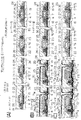
まず、図1の(1)に示すように、石英ガラス、透明性結晶化ガラスなどの絶縁基板1の一主面において、少なくともTFT形成領域に、フォトレジスト2を所定パターンに形成し、これをマスクとして例えばCF4 プラズマのF+ イオン3を照射し、リアクティブイオンエッチング(RIE)などの汎用フォトリソグラフィ及びエッチング(フォトエッチング)によって基板1に段差4を適当な形状及び寸法で複数個形成する。
【0070】
この場合、絶縁基板1として石英ガラス、透明性結晶化ガラス、セラミック等(但し、後述の透過型LCDでは、不透明のセラミック基板や低透明性の結晶化ガラスは使用できない。)の高耐熱性基板(8〜12インチφ、700〜800μm厚)が使用可能である。また、段差4は、後述の単結晶シリコンのエピタキシャル成長時のシードとなるものであって、深さd0.1〜0.4μm、幅w2〜10μm、長さ(紙面垂直方向)10〜20μmであってよく、底辺と側面のなす角(底角)は直角とする。なお、基板1の表面には、ガラス基板からのNaイオンなどの拡散防止のため、SiN膜(例えば50〜200nm厚)と必要に応じてシリコン酸化膜(以後SiO2 膜と呼ぶ。)(例えば約100nm厚)を予め連続形成してよい。
【0071】
次いで、図1の(2)に示すように、フォトレジスト2の除去後に、絶縁基板1の一主面において、段差4を含む少なくともTFT形成領域に、結晶性サファイア膜(厚さ20〜200nm)50を形成する。この結晶性サファイア膜50は、高密度プラズマCVD法や、触媒CVD法(特開昭63−40314号公報参照)等により、トリメチルアルミニウムガスなどを酸化性ガス(酸素・水分)で酸化し、結晶化させて作成する。絶縁基板1として高耐熱性ガラス基板(8〜12インチφ、700〜800μm厚)が使用可能である。
【0072】
次いで、図1の(3)に示すように、段差4を含む結晶性サファイア膜50上の全面において、シリコンを約1重量%含有するシリコン・インジウム溶融液6を、900〜930℃に加熱された基板1上に塗布する。或いは、溶融液中に基板1をディッピングするか、或いは、溶融液表面を徐々に移動させてフローティングさせる方法や、噴流式、超音波作用下での接触方式も可能である。
【0073】
次いで、基板1を数分〜数10分間保持した後、徐々に冷却する(ディッピングの場合は徐々に引き上げる)ことによって、インジウムに溶解していたシリコンは、結晶性サファイア膜50(更には段差4の底辺の角部)をシード(種)として図2の(4)に示すようにヘテロエピタキシャル成長し、厚さ例えば0.1μm程度のP型単結晶シリコン層7として析出する。ディッピング法及びフローティング法では、溶融液組成、温度、引き上げ速度などの管理が容易であり、エピタキシャル成長層の厚みやP型キャリア不純物濃度を容易にコントロールできる。
【0074】
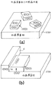
上記のようにして堆積した単結晶シリコン層7は結晶性サファイア膜50が単結晶シリコンと良好な格子整合を示すために、例えば(100)面が基板上にヘテロエピタキシャル成長する。この場合、段差4もグラフォエピタキシャル成長と称される公知の現象を加味したヘテロエピタキシャル成長に寄与し、より結晶性の高い単結晶シリコン層7が得られる。これについては、図8に示すように、非晶質基板(ガラス)1に上記の段差4の如き垂直な壁を作り、この上にエピタキシー層を形成すると、図8(a)のようなランダムな面方位であったものが図8(b)のように(100)面が段差4の面に沿って結晶成長する。この単結晶粒の大きさは、温度・時間に比例して大きくなるが、温度・時間を低く、短くする時は、上記段差の間隔を短くしなければならない。また、上記段差の形状を図9(a)〜(f)のように種々に変えることによって、成長層の結晶方位を制御することができる。MOSトランジスタを作成する場合は、(100)面が最も多く採用されている。要するに、段差4の断面形状は、底辺角部の角度(底角)が直角をはじめ、上端から下端にかけて内向き又は外向きに傾斜していてもよく、結晶成長が生じ易い特定方向の面を有していればよい。段差4の底角は通常は直角又は90°以下が望ましく、その底面の角部は僅かな曲率を有しているのがよい。
【0075】
こうして、ヘテロエピタキシャル成長によって基板1上に単結晶シリコン層7を析出させた後、図2の(5)のように、表面側に析出したインジウム膜6Aを塩酸、硫酸などのよって溶解除去(この際、低級シリコン酸化膜が生成しないように後処理)し、単結晶シリコン層7をチャンネル領域とするトップゲート型MOSTFTの作製を行う。
【0076】
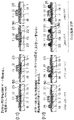
まず、上記のヘテロエピタキシャル成長による単結晶シリコン層7はインジウムの含有によってP型化しているが、そのP型不純物濃度はばらついているので、pチャンネルMOSTFT部をフォトレジスト(図示せず)でマスクし、P型不純物イオン(例えばB+ )を10kVで2.7×10¹¹atoms/cm2 のドーズ量でドーピングし、比抵抗を調整する。また、図2の(6)に示すように、pMOSTFT形成領域の不純物濃度制御のため、nMOSTFT部をフォトレジスト60でマスクし、N型不純物イオン(例えばP+ )65を10kVで1×10¹¹atoms/cm2 のドーズ量でドーピングし、N型ウエル7Aを形成する。
【0077】
次いで、図3の(7)に示すように、単結晶シリコン層7の全面上に、プラズマCVD、高密度プラズマCVD、触媒CVD法等でSiO2 (約200nm厚)とSiN(約100nm厚)をこの順に連続形成してゲート絶縁膜8を形成し、更に、モリブデン・タンタル(Mo・Ta)合金のスパッタ膜9(500〜600nm厚)を形成する。
【0078】
次いで、図3の(8)に示すように、汎用のフォトリソグラフィ技術により、表示領域のTFT部と、周辺駆動領域のTFT部とのそれぞれの段差領域(凹部内)にフォトレジストパターン10を形成し、連続したエッチングにより、(Mo・Ta)合金のゲート電極11とゲート絶縁膜(SiN/SiO2 )12とを形成し、単結晶シリコン層7を露出させる。(Mo・Ta)合金膜9は酸系エッチング液、SiNはCF4 ガスのプラズマエッチング、SiO2 はフッ酸系エッチング液で処理する。
【0079】
次いで、図3の(9)に示すように、周辺駆動領域のnMOS及びpMOSTFT全部と、表示領域のnMOSTFTのゲート部をフォトレジスト13でカバーし、露出したnMOSTFTのソース/ドレイン領域にリンイオン14を例えば20kVで5×1013atoms/cm2 のドーズ量でドーピング(イオン注入)して、N- 型層からなるLDD部15を自己整合的(セルフアライン)に形成する。
【0080】
次いで、図4の(10)に示すように、周辺駆動領域のpMOSTFT全部と、周辺駆動領域のnMOSTFTのゲート部と、表示領域のnMOSTFTのゲート及びLDD部とをフォトレジスト16でカバーし、露出した領域にリン又はひ素イオン17を例えば20kVで5×10¹⁵atoms/cm2 のドーズ量でドーピング(イオン注入)して、nMOSTFTのN+ 型層からなるソース部18及びドレイン部19とLDD部15とを形成する。
【0081】
次いで、図4の(11)に示すように、周辺駆動領域のnMOSTFT及び表示領域のnMOSTFTの全部とpMOSTFTのゲート部をフォトレジスト20でカバーし、露出した領域にボロンイオン21を例えば10kVで5×10¹⁵atoms/cm2 のドーズ量でドーピング(イオン注入)してpMOSTFTのP+ 層のソース部22及びドレイン部23を形成する。なお、この作業は、nMOS周辺駆動回路の場合はpMOSTFTが無いので、不要な作業である。
【0082】
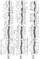
次いで、図4の(12)に示すように、TFT、ダイオードなどの能動素子部や、抵抗、インダクタンスなどの受動素子部をアイランド化するため、フォトレジスト24を設け、周辺駆動領域及び表示領域のすべての能動素子部及び受動素子部以外の単結晶シリコン薄膜層を汎用フォトリソグラフィ及びエッチング技術で除去する。エッチング液はフッ酸系である。
【0083】
次いで、図5の(13)に示すように、プラズマCVD、高密度プラズマCVD、触媒CVD法等により、SiO2 膜(約200nm厚)及びリンシリケートガラス(PSG)膜(約300nm厚)をこの順に全面に連続形成して保護膜25を形成する。
【0084】
そして、この状態で単結晶シリコン層を活性化処理する。この活性化においてハロゲン等のランプアニール条件は約1000℃、約10秒程度であり、これに耐えるゲート電極材が必要であるが、高融点のMo・Ta合金は適している。このゲート電極材は従って、ゲート部のみならず配線として広範囲に亘って引き廻して設けることができる。なお、ここでは高価なエキシマレーザーアニールは使用しないが、仮に利用するとすれば、その条件はXeCl(308nm波長)で全面、又は能動素子部及び受動素子部のみの選択的な90%以上のオーバーラップスキャンニングが望ましい。
【0085】
次いで、図5の(14)に示すように、汎用フォトリソグラフィ及びエッチング技術により、周辺駆動回路の全TFTのソース/ドレイン部、及び表示用TFTのソース部のコンタクト用窓開けを行う。
【0086】
そして、全面に500〜600nm厚のアルミニウム又はアルミニウム合金、例えば1%Si入りアルミニウム又は1〜2%銅入りアルミニウム、銅等のスパッタ膜を形成し、汎用フォトリソグラフィ及びエッチング技術により、周辺駆動回路及び表示部のすべてのTFTのソース電極26と周辺駆動回路部のドレイン電極27を形成すると同時に、データライン及びゲートラインを形成する。その後に、フォーミングガス(N2 +H2 )中、約400℃/1hで、シンター処理する。
【0087】
次いで、図5の(15)に示すように、プラズマCVD、高密度プラズマCVD、触媒CVD法等により、PSG膜(約300nm厚)及びSiN膜(約300nm厚)からなる絶縁膜36を全面に形成する。次いで、表示用TFTのドレイン部のコンタクト用窓開けを行う。なお、画素部のSiO2 、PSG及びSiN膜は除去する必要はない。
【0088】
反射型液晶表示装置の基本的要件としては、液晶パネルの内部に入射光を反射させる機能と散乱させる機能を合わせ持たなければならない。これは、ディスプレイに対する観察者の方向はほぼ決まっているが、入射光の方向が一義的に決められないためである。このため、任意の方向に点光源が存在することを想定して反射板の設計を行う必要がある。そこで、図6の(16)に示すように、全面に、スピンコート等で2〜3μm厚みの感光性樹脂膜28を形成し、図6の(17)に示すように、汎用フォトリソグラフィ及びエッチング技術により、少なくとも画素部に最適な反射特性と視野角特性を得るための凹凸形状パターンを形成し、リフローさせて凹凸粗面28Aからなる反射面下部を形成する。同時に表示用TFTのドレイン部のコンタクト用の樹脂窓開けを行う。
【0089】
次いで、図6の(18)に示すように、全面に400〜500nm厚のアルミニウム又は1%Si入りアルミニウム等のスパッタ膜を形成し、汎用フォトリソグラフィ及びエッチング技術により、画素部以外のアルミニウム膜等を除去し、表示用TFTのドレイン部19と接続した凹凸形状のアルミニウム等の反射部29を形成する。これは表示用の画素電極として用いられる。その後に、フォーミングガス中、約300℃/1hでシンター処理し、コンタクトを十分にする。尚、反射率を高めるために、アルミニウム系に代えて銀又は銀合金を使用してもよい。
【0090】
以上のようにして、段差4を含む結晶性サファイア膜50を高温ヘテロエピタキシャル成長のシードとして単結晶シリコン層7を形成し、この単結晶シリコン層7を用いた表示部及び周辺駆動回路部にそれぞれ、トップゲート型のnMOSLDD−TFT、pMOSTFT及びnMOSTFTで構成するCMOS回路を作り込んだ表示部−周辺駆動回路部一体型のアクティブマトリクス基板30を作製することができる。
【0091】
次に、このアクティブマトリクス基板(駆動基板)30を用いて、反射型液晶表示装置(LCD)を製造する方法を図7について説明する。以降では、このアクティブマトリクス基板をTFT基板と呼称する。
【0092】
このLCDの液晶セルを面面組立で作製する場合(2インチサイズ以上の中/大型液晶パネルに適している。)、まずTFT基板30と、全面ベタのITO(Indium tin oxide)電極31を設けた対向基板32の素子形成面に、ポリイミド配向膜33、34を形成する。このポリイミド配向膜はロールコート、スピンコート等により50〜100nm厚に形成し、180℃/2hで硬化キュアする。
【0093】
次いで、TFT基板30と対向基板32をラビング、又は光配向処理する。ラビングバフ材にはコットンやレーヨン等があるが、バフかす(ゴミ)やリタデーション等の面からはコットンの方が安定している。光配向は非接触の線型偏光紫外線照射による液晶分子の配向技術である。なお、配向には、ラビング以外にも、偏光又は非偏光を斜め入射させることによって高分子配向膜を形成することができる(このような高分子化合物は、例えばアゾベンゼンを有するポリメチルメタクリレート系高分子等がある)。
【0094】
次いで、洗浄後に、TFT基板30側にはコモン剤塗布、対向基板32側にはシール剤塗布する。ラビングバフかす除去のために、水、又はIPA(イソプロピルアルコール)洗浄する。コモン剤は導電性フィラーを含有したアクリル、又はエポキシアクリレート、又はエポキシ系接着剤であってよく、シール剤はアクリル、又はエポキシアクリレート、又はエポキシ系接着剤であってよい。加熱硬化、紫外線照射硬化、紫外線照射硬化+加熱硬化のいずれも使用できるが、重ね合せの精度と作業性からは紫外線照射硬化+加熱硬化タイプが良い。
【0095】
次いで、対向基板32側に所定のギャップを得るためのスペーサを散布し、TFT基板30と所定の位置で重ね合せる。対向基板32側のアライメントマークとTFT基板30側のアライメントマークとを精度よく合わせた後に、紫外線照射してシール剤を仮硬化させ、その後に一括して加熱硬化する。
【0096】
次いで、スクライブブレークして、TFT基板30と対向基板32を重ね合せた単個の液晶パネルを作成する。
【0097】
次いで、液晶35を両基板30−32間のギャップ内に注入し、注入口を紫外線接着剤で封止後に、IPA洗浄する。液晶の種類はなんでも良いが、例えばネマティック液晶を用いる高速応答のTN(ツイストネマティック)モードが一般的である。
【0098】
次いで、加熱急冷処理して、液晶35を配向させる。
【0099】
次いで、TFT基板30のパネル電極取り出し部にフレキシブル配線を異方性導電膜の熱圧着で接続し、更に対向基板32に偏光板を貼合わせる。
【0100】
また、液晶パネルの面単組立の場合(2インチサイズ以下の小型液晶パネルに適している。)、上記と同様、TFT基板30と対向基板32の素子形成面に、ポリイミド配向33、34を形成し、両基板をラビング、又は非接触の線型偏光紫外線光の配向処理する。
【0101】
次いで、TFT基板30と対向基板32をダイシング又はスクライブブレークで単個に分割し、水又はIPA洗浄する。TFT基板30にはコモン剤塗布、対向基板32にはスペーサ含有のシール剤塗布し、両基板を重ね合せる。これ以降のプロセスは上記に準ずる。
【0102】
上記した反射型LCDにおいて、対向基板32はCF(カラーフィルタ)基板であって、カラーフィルタ層46をITO電極31下に設けたものである。対向基板32側からの入射光は反射膜29で効率良く反射されて対向基板32側から出射する。
【0103】
他方、TFT基板30として、図7のような上記した基板構造以外に、TFT基板30にカラーフィルタを設けたオンチップカラーフィルタ(OCCF)構造のTFT基板とするときには、対向基板32にはITO電極がベタ付け(又はブラックマスク付きのITO電極がベタ付け)される。
【0104】
なお、図12に示した補助容量CS を画素部に組み込む場合は、上記した基板1上に設けた誘電体層(図示せず)を単結晶シリコンのドレイン領域19と接続すればよい。
【0105】
以上に説明したように、本実施の形態によれば、次の如き顕著な作用効果が得られる。
【0106】
(a)所定形状/寸法の段差4を設けた基板1に結晶性サファイア膜50を形成し、これをシードとして高温ヘテロエピタキシャル成長(但し、成長時の加熱温度は900〜930℃と比較的低温)させることにより、540cm2 /v・sec以上の高い電子移動度の単結晶シリコン薄膜7が得られるので、高性能ドライバ内蔵のLCDの製造が可能となる。段差4はこのヘテロエピタキシャル成長を促進するため、より結晶性の高い単結晶シリコン層7が得られる。
【0107】
(b)この単結晶シリコン層は、従来のアモルファスシリコン薄膜や多結晶シリコン薄膜に比べて、単結晶シリコン基板並の高い電子及び正孔移動度を示すので、これによる単結晶シリコントップゲート型MOSTFTは、高いスイッチング特性と低リーク電流のLDD構造を有するnMOS又はpMOS又はcMOSTFTの表示部と、高い駆動能力のcMOS、nMOS又はpMOSTFT又はこれらの混在からなる周辺駆動回路部とを一体化した構成が可能となり、高画質、高精細、狭額縁、大画面、高効率の表示パネルが実現する。この単結晶シリコン層7は十分に高い正孔移動度を示すため、電子と正孔をそれぞれ単独でも、或いは双方を組み合せて駆動する周辺駆動回路を作製でき、これをnMOS又はpMOS又はcMOSのLDD構造の表示用TFTと一体化したパネルを実現できる。また、小型〜中型パネルの場合には、周辺の一対の垂直駆動回路の一方を省略できる可能性がある。
【0108】
(c)そして、上記したヘテロエピタキシャル成長時の加熱処理温度は930℃以下が可能であるから、絶縁基板上に比較的低温(例えば900〜930℃以下)で単結晶シリコン膜7を均一に形成することができる。なお、基板としては、石英ガラスや結晶化ガラス、セラミック基板などが使用可能である。
【0109】
(d)固相成長法の場合のような中温で長時間のアニールや、エキシマレーザーアニールが不要となるから、生産性が高く、高価な製造設備が不要でコストダウンが可能となる。
【0110】
(e)この高温ヘテロエピタキシャル成長では、結晶性サファイア膜の結晶性、インジウム・シリコン組成比、段差の形状、基板加熱温度、溶融液温度、冷却速度、添加するN型又はP型キャリア不純物濃度等の調整により、広範囲のP型不純物濃度と高移動度の単結晶シリコン薄膜が容易に得られるので、Vth(しきい値)調整が容易であり、低抵抗化による高速動作が可能である。
【0111】
(f)表示アレイ部上にカラーフィルタを作り込めば、表示パネルの開口率、輝度等の改善をはじめ、カラーフィルタ基板の省略、生産性改善等によるコストダウンが実現する。
【0112】
(g)結晶性サファイア膜などの上記物質層は、様々な原子の拡散バリアになるため、ガラス基板からの不純物の拡散を抑制することができる。
【0113】
<第2の実施の形態>
図14〜図16について、本発明の第2の実施の形態を説明する。
【0114】
本実施の形態は、上述の第1の実施の形態と比べて、同様のトップゲート型MOSTFTを表示部及び周辺駆動回路部に有するが、上述の第1の実施の形態とは異なって、透過型LCDに関するものである。即ち、図1の(1)から図5の(15)に示す工程までは同様であるが、その工程後に、図14の(16)に示すように、絶縁膜25、36に表示用TFTのドレイン部コンタクト用の窓開け19を行うと同時に、透過率向上のために画素開口部の不要なSiO2 、PSG及びSiN膜を除去する。
【0115】
次いで、図14の(17)に示すように、全面にスピンコート等で2〜3μm厚みの感光性アクリル系透明樹脂の平坦化膜28Bを形成し、汎用フォトリソグラフィにより、表示用TFTのドレイン側の透明樹脂28Bの窓開けを行い、所定条件で硬化させる。
【0116】
次いで、図14の(18)に示すように、全面に130〜150nm厚のITOスパッタ膜を形成し、汎用フォトリソグラフィ及びエッチング技術により、表示用TFTのドレイン部19とコンタクトしたITO透明電極41を形成する。そして、熱処理(フォーミングガス中、200〜250℃/1h)により、表示用TFTのドレインとITOのコンタクト抵抗の低減化とITO透明度の向上を図る。
【0117】
そして、図15に示すように、対向基板32と組み合わせ、上述の第1の実施の形態と同様にして透過型LCDを組み立てる。但し、TFT基板側にも偏光板を貼り合わせる。この透過型LCDでは、実線のように透過光が得られるが、一点鎖線のように対向基板32側からの透過光が得られるようにもできる。
【0118】
この透過型LCDの場合、次のようにしてオンチップカラーフィルタ(OCCF)構造とオンチップブラック(OCB)構造を作製することができる。
【0119】
即ち、図1の(1)〜図5の(14)までの工程は上記の工程に準じて行うが、その後、図16の(15)に示すように、PSG/SiO2 の絶縁膜25のドレイン部も窓開けしてドレイン電極用のアルミニウム埋込み層41Aを形成した後、SiN/PSGの絶縁膜36を形成する。
【0120】
次いで、図16の(16)に示すように、R、G、Bの各色を各セグメント毎に顔料分散したフォトレジスト61を所定厚さ(1〜1.5μm)で形成した後、図16の(17)に示すように、汎用フォトリソグラフィ技術で所定位置(各画素部)のみを残すパターニングで各カラーフィルタ層61(R)、61(G)、61(B)を形成する(オンチップカラーフィルタ構造)。この際、ドレイン部の窓開けも行う。なお、不透明なセラミック基板や低透過率のガラス及び耐熱性樹脂基板は使用できない。
【0121】
次いで、図16の(17)に示すように、表示用TFTのドレインに連通するコンタクトホールに、カラーフィルタ層上にかけてブラックマスク層となる遮光層43を金属のパターニングで形成する。例えば、スパッタ法により、モリブデンを200〜250nm厚で成膜し、表示用TFTを覆って遮光する所定の形状にパターニングする(オンチップブラック構造)。
【0122】
次いで、図16の(18)に示すように、透明樹脂の平坦化膜28Bを形成し、更にこの平坦化膜に設けたスルーホールにITO透明電極41を遮光層43に接続するように形成する。
【0123】
このように、表示アレイ部上に、カラーフィルタ61やブラックマスク43を作り込むことにより、液晶表示パネルの開口率を改善し、またバックライトも含めたディスプレイモジュールの低消費電力化が実現する。
【0124】
<第3の実施の形態>
本発明の第3の実施の形態を説明する。
【0125】
本実施の形態は、歪点の低いガラス基板に上述した段差(凹部)4及び結晶性サファイア膜50を形成し、これをシードとしてインジウム・ガリウム・シリコン又はガリウム・シリコン溶融液から単結晶シリコン層を低温ヘテロエピタキシャル成長させ、これを用いてトップゲート型MOSTFTを構成したアクティブマトリクス反射型液晶表示装置(LCD)に関するものである。
【0126】
即ち、本実施の形態では、上述の第1の実施の形態と比べて、図1の(1)に示す工程で、基板1として、歪点又は最高使用温度が例えば600℃程度と低いガラス、例えばホウケイ酸ガラスやアルミノケイ酸ガラスなどのガラス基板を用いる。これは、安価でかつ大型化が容易であり、薄板大型化(例えば500×600×0.1〜1.1mm厚)すればロール化/長尺化が可能である。もちろん、石英基板や結晶化ガラス基板も採用することができる。
【0127】
そして、上述と同様に段差4及び結晶性サファイア膜50を形成した後、図1の(3)に示す工程で、結晶性サファイア膜50上に、シリコンを含有するインジウム・ガリウム溶融液(又はガリウム溶融液)を塗布する。
【0128】
次いで、徐々に冷却することによって、インジウム・ガリウム(又はガリウム)に溶解していたシリコンは、結晶性サファイア膜50(更には段差4の底辺の角部)をシード(種)として図2の(4)に示すようにヘテロエピタキシャル成長し、厚さ例えば0.1μm程度の単結晶シリコン層7として析出する。
【0129】
この場合、単結晶シリコン層7は上述したと同様に(100)面が基板上にヘテロエピタキシャル成長したものであるが、上記段差の形状を図9(a)〜(f)のように種々に変えることによって、成長層の結晶方位を制御することができる。
【0130】
こうして、低温ヘテロエピタキシャル成長によって基板1上に単結晶シリコン層7を析出させた後、図2の(5)のように、表面側のインジウム・ガリウム(又はガリウム)を塩酸、硫酸などによって溶解除去する。
【0131】
しかる後、単結晶シリコン層7を用いて上述の第1の実施の形態と同様にして表示部及び周辺駆動回路部にトップゲート型のMOSTFTの作製を行う。また図7に示した構造は、本実施の形態でも同様に適用されてよい。
【0132】
本実施の形態によれば、上述した第1の実施の形態で述べた作用効果に加え、次の如き顕著な作用効果が得られる。
【0133】
(a)ガラス基板1上に、約300〜600℃又は420〜600℃と更に低温でのヘテロエピタキシャル成長により、シリコン単結晶薄膜7を均一に形成することができる。
【0134】
(b)従って、ガラス基板のみならず、有機基板などの絶縁基板上に、シリコン単結晶薄膜を形成できるため、歪点が低く、低コストで物性も良好な基板材質を任意に選択でき、また、基板の大型化も可能となる。ガラス基板や有機基板は、石英基板やセラミック基板に比べて、安価に作成することができ、さらに薄板化/長尺化/ロール化が可能であるので、シリコン単結晶薄膜を形成した薄板を長尺/ロール化した大型ガラス基板などを生産性良く、安価に作製することができる。ガラス基板として、ガラス歪点(又は最高使用温度)が低い(例えば500℃)ガラスを用いると、この上層へガラス内部からその構成元素が拡散して、トランジスタ特性に影響する場合には、これを抑制する目的で、バリア層薄膜(例えばシリコンナイトライド:厚さ50〜200nm程度)を形成すればよい。しかし、これは、結晶性サファイア膜50の拡散防止作用によって、省略可能である。
【0135】
(c)この低温ヘテロエピタキシャル成長では、インジウム・ガリウム膜のインジウム/ガリウム組成比、加熱温度、冷却速度等の調整により、広範囲のP型不純物濃度と高移動度の単結晶シリコン薄膜が容易に得られるので、Vth調整が容易で低抵抗化による高速動作が可能である。
【0136】
<第4の実施の形態>
本発明の第4の実施の形態を説明する。
【0137】
本実施の形態は、上述の第3の実施の形態と比べて透過型LCDに関するものであってその製造工程は上述の第2の実施の形態で述べたと同様、インジウム・ガリウム溶融液を用いた低温ヘテロエピタキシャル成長によって単結晶シリコン薄膜を形成することができる。
【0138】
そして、この単結晶シリコン薄膜を用い、上述した第2の実施の形態で述べたと同様、図14〜図16に示した工程によって透過型LCDを作製することができる。但し、不透明のセラミック基板や、不透明又は低透過率の有機基板は適していない。
【0139】
従って、本実施の形態では、上述した第3の実施の形態及び第2の実施の形態の双方の優れた作用効果を併せ持つことができる。即ち、上述した第1の実施の形態の有する作用効果に加え、ホウケイ酸ガラスや耐熱性のポリイミド等の有機基板などの低コストで薄板、長尺化が可能な基板1を用い得ること、インジウム/ガリウム組成比によって単結晶シリコン薄膜7の導電型やVthの調整が容易となること、表示アレイ部上にカラーフィルタ42やブラックマスク43を作りこむことにより、液晶表示パネルの開口率を改善し、またバックライトも含めたディスプレイモジュールの低消費電力化が実現することである。
【0140】
<第5の実施の形態>
図17〜図25は、本発明の第5の実施の形態を示すものである。
【0141】
本実施の形態では、周辺駆動回路部は上述した第1の実施の形態と同様のトップゲート型のpMOSTFTとnMOSTFTとからなるCMOS駆動回路で構成する。表示部は反射型ではあるが、TFTを各種ゲート構造のものとして、種々の組み合わせにしている。
【0142】
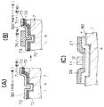
即ち、図17(A)は、上述した第1の実施の形態と同様のトップゲート型のnMOSLDD−TFTを表示部に設けているが、図17(B)に示す表示部にはボトムゲート型のnMOSLDD−TFT、図17(C)に示す表示部にはデュアルゲート型のnMOSLDD−TFTをそれぞれ設けている。これらのボトムゲート型、デュアルゲート型MOSTFTのいずれも、後述のように、周辺駆動回路部のトップゲート型MOSTFTと共通の工程で作製可能であるが、特にデュアルゲート型の場合には上下のゲート部によって駆動能力が向上し、高速スイッチングに適し、また上下のゲート部のいずれかを選択的に用いて場合に応じてトップゲート型又はボトムゲート型として動作させることもできる。
【0143】
なお、図17(B)のボトムゲート型MOSTFTにおいて、図中の71はMo・Ta等のゲート電極であり、72はSiN膜及び73はSiO2 膜であってゲート絶縁膜を形成し、このゲート絶縁膜上にはトップゲート型MOSTFTと同様の単結晶シリコン層を用いたチャンネル領域等が形成されている。また、図17(C)のデュアルゲート型MOSTFTにおいて、下部ゲート部はボトムゲート型MOSTFTと同様であるが、上部ゲート部は、ゲート絶縁膜73をSiO2 膜とSiN膜で形成し、この上に上部ゲート電極74を設けている。但し、いずれにおいても、ヘテロエピタキシャル成長時のシードであると同時に単結晶シリコン膜の成長を促進し、その結晶性を高める作用を有する段差4の外側に各ゲート部を構成している。
【0144】
次に、上記のボトムゲート型MOSTFTの製造方法を図18〜図22で、上記のデュアルゲート型MOSTFTの製造方法を図23〜図25でそれぞれ説明する。なお、周辺駆動回路部のトップゲート型MOSTFTの製造方法は図1〜図6において述べたものと同じであるので、ここでは図示を省略している。
【0145】
表示部において、ボトムゲート型MOSTFTを製造するには、まず、図18の(1)に示すように、基板1上に、モリブデン/タンタル(Mo・Ta)合金のスパッタ膜71(500〜600nm厚)を形成する。
【0146】
次いで、図18の(2)に示すように、フォトレジスト70を所定パターンに形成し、これをマスクにしてMo・Ta膜71をテーパエッチングし、側端部71aが台形状に20〜45度でなだらかに傾斜したゲート電極71を形成する。
【0147】
次いで、図18の(3)に示すように、フォトレジスト70の除去後に、モリブデン・タンタル合金膜71を含む基板1上に、プラズマCVD法等により、SiN膜(約100nm厚)72とSiO2 膜(約200nm厚)73とを、この順に積層したゲート絶縁膜を形成する。
【0148】
次いで、図18の(4)に示すように、図1の(1)と同じ工程において、少なくともTFT形成領域に、フォトレジスト2を所定パターンに形成し、これをマスクとして上述したと同様に基板1上のゲート絶縁膜に(更には基板1にも)段差4を適当な形状及び寸法で複数個形成する。この段差4は、後述の単結晶シリコンのヘテロエピタキシャル成長時のシードであると同時に単結晶シリコン膜の成長を促進し、その結晶性を高める作用を有するものであって、深さd=0.3〜0.4μm、幅w=2〜3μm、長さ(紙面垂直方向)=10〜20μmであってよく、底辺と側面のなす角(底角)は直角とする。
【0149】
次いで、図18の(5)に示すように、フォトレジスト2の除去後に、図1の(2)と同じ工程において、上述したと同様に絶縁基板1の一主面において、段差4を含む少なくともTFT形成領域に、結晶性サファイア膜(厚さ20〜200nm)50を形成する。
【0150】
次いで、図19の(6)に示すように、図2の(3)と同じ工程においてシリコンを含有するインジウム(又はインジウム・ガリウム又はガリウム)溶融液6を塗布する。
【0151】
次いで、図19の(7)に示すように、図2の(4)と同じ工程において、単結晶シリコンをヘテロエピタキシャル成長し、厚さ例えば0.1μm程度の単結晶シリコン層7として析出させる。この際、下地のゲート電極71の側端部71aはなだらかな傾斜面となっているので、この面上には、段差4によるヘテロエピタキシャル成長を阻害せず、段切れなしに単結晶シリコン層7が成長することになる。
【0152】
次いで、図19の(8)に示すように、インジウム等の膜6Aを除去し、更に図2の(6)〜図3の(8)の工程を経た後、図19の(9)に示すように、図3の(9)と同じ工程において、表示部のnMOSTFTのゲート部をフォトレジスト13でカバーし、露出したnMOSTFTのソース/ドレイン領域にリンイオン14をドーピング(イオン注入)して、N- 型層からなるLDD部15を自己整合的に形成する。このとき、ボトムゲート電極71の存在によって表面高低差(又はパターン)を認識し易く、フォトレジスト13の位置合わせ(マスク合わせ)を行い易く、アライメントずれが生じにくい。
【0153】
次いで、図20の(10)に示すように、図4の(10)と同じ工程において、nMOSTFTのゲート部及びLDD部をフォトレジスト16でカバーし、露出した領域にリン又はひ素イオン17をドーピング(イオン注入)して、nMOSTFTのN+ 型層からなるソース部18及びドレイン部19を形成する。
【0154】
次いで、図22の(11)に示すように、図4の(11)と同じ工程において、nMOSTFTの全部をフォトレジスト20でカバーし、ボロンイオン21をドーピング(イオン注入)して周辺駆動回路部のpMOSTFTのP+ 層のソース部及びドレイン部を形成する。
【0155】
次いで、図22の(12)に示すように、図4の(12)と同じ工程において、能動素子部と受動素子部をアイランド化するため、フォトレジスト24を設け、単結晶シリコン薄膜層を汎用フォトリソグラフィ及びエッチング技術で選択的に除去する。
【0156】
次いで、図22の(13)に示すように、図5の(13)と同じ工程において、プラズマCVD、高密度プラズマCVD、触媒CVD法等により、SiO2 膜53(約300nm厚)とリンシリケートガラス(PSG)膜54(約300nm厚)をこの順に全面に形成する。なお、SiO2 膜53とPSG膜54は上述した保護膜25に相当するものである。そして、この状態で単結晶シリコン膜を上述したと同様に活性化処理する。
【0157】
次いで、図21の(14)に示すように、図5の(14)と同じ工程において、汎用フォトリソグラフィ及びエッチング技術により、ソース部のコンタクト用窓開けを行う。そして、全面に400〜500nm厚のアルミニウム等のスパッタ膜を形成し、汎用フォトリソグラフィ及びエッチング技術により、TFTのソース電極26を形成すると同時に、データライン及びゲートラインを形成する。その後に、フォーミングガス中、約400℃/1hで、シンター処理する。
【0158】
次いで、図21の(15)に示すように、図5の(15)と同じ工程において、高密度プラズマCVD、触媒CVD法等により、PSG膜(約300nm厚)及びSiN膜(約300nm厚)からなる絶縁膜36を全面に形成し、表示用のTFTのドレイン部のコンタクト用窓開けを行う。
【0159】
次いで、図21の(16)に示すように、図6の(16)と同じ工程において、スピンコート等で2〜3μm厚みの感光性樹脂膜28を形成し、図21の(17)に示すように、汎用フォトリソグラフィ及びエッチング技術により、少なくとも画素部に最適な反射特性と視野角特性を得るような凹凸形状パターンを形成し、リフローさせて凹凸粗面28Aからなる反射面下部を形成する。同時に表示用TFTのドレイン部のコンタクト用の樹脂窓開けを行う。
【0160】
次いで、図21の(17)に示すように、図6の(18)と同じ工程において、全面に400〜500nm厚のアルミニウム等のスパッタ膜を形成し、汎用フォトリソグラフィ及びエッチング技術により、表示用TFTのドレイン部19と接続した凹凸形状のアルミニウム等の反射部29を形成する。
【0161】
以上のようにして、結晶性サファイア膜50及び段差4をヘテロエピタキシャル成長のシードとして形成された単結晶シリコン層7を用いた表示部にボトムゲート型のnMOSLDD−TFT(周辺部ではトップゲート型のpMOSTFT及びnMOSTFTからなるCMOS駆動回路)を作り込んだ表示部−周辺駆動回路部一体型のアクティブマトリクス基板30を作製することができる。
【0162】
図22は、表示部に設ける上記のボトムゲート型MOSTFTのゲート絶縁膜をMo・Taの陽極酸化法で形成した例を示す。
【0163】
即ち、図18の(2)の工程後に、図22の(3)に示すようにモリブデン・タンタル合金膜71を公知の陽極酸化処理することによって、その表面にTa2 O5 からなるゲート絶縁膜74を100〜200nm厚に形成する。
【0164】
この後の工程は、図22の(4)に示すように、図18の(4)〜図19の(8)の工程と同様にして段差4、更には結晶性サファイア膜50を形成し、単結晶シリコン膜7をヘテロエピタキシャル成長した後、図19の(9)〜図21の(17)の工程と同様にして図22の(5)に示すように、アクティブマトリクス基板30を作製する。
【0165】
次に、表示部において、デュアルゲート型MOSTFTを製造するには、まず、図18の(1)〜図19の(8)までの工程は、上述したと同様に行う。
【0166】
即ち、図23の(9)に示すように、絶縁膜72、73及び基板1に段差4を形成し、更に、結晶性サファイア膜50及び段差4をシードとして単結晶シリコン層7をヘテロエピタキシャル成長させる。次いで、図3の(7)と同じ工程において、単結晶シリコン薄膜7上の全面に、プラズマCVD、触媒CVD等によりSiO2 膜(約200nm厚)とSiN膜(約100nm厚)をこの順に連続形成して絶縁膜80(これは上述の絶縁膜8に相当)を形成し、更に、Mo・Ta合金のスパッタ膜81(500〜600nm厚)(これは上述のスパッタ膜9に相当)を形成する。
【0167】
次いで、図23の(10)に示すように、図3の(8)と同じ工程において、フォトレジストパターン10を形成し、連続したエッチングによりMo・Ta合金のトップゲート電極82(これは上述のゲート電極12に相当)と、ゲート絶縁膜83(これは上述のゲート絶縁膜11に相当)を形成し、単結晶シリコン薄膜層7を露出させる。
【0168】
次いで、図23の(11)に示すように、図3の(9)と同じ工程において、nMOSTFTのトップゲート部をフォトレジスト13でカバーし、露出した表示用のnMOSTFTのソース/ドレイン領域にリンイオン14をドーピング(イオン注入)して、N- 型層のLDD部15を形成する。
【0169】
次いで、図23(12)に示すように、図4の(10)と同じ工程において、nMOSTFTのゲート部及びLDD部をフォトレジスト16でカバーし、露出した領域にリン又はひ素イオン17をドーピング(イオン注入)して、nMOSTFTのN+ 型層からなるソース部18及びドレイン部19を形成する。
【0170】
次いで、図24の(13)に示すように、図4の(11)と同じ工程において、pMOSTFTのゲート部をフォトレジスト20でカバーし、露出した領域にボロンイオン21をドーピング(イオン注入)して周辺駆動回路部のpMOSTFTのP+ 層のソース部及びドレイン部を形成する。
【0171】
次いで、図24の(14)に示すように、図4の(12)と同じ工程において、能動素子部と受動素子部をアイランド化するため、フォトレジスト24を設け、能動素子部と受動素子部以外の単結晶シリコン薄膜層を汎用フォトリソグラフィ及びエッチング技術で選択的に除去する。
【0172】
次いで、図24の(15)に示すように、図5の(13)と同じ工程において、プラズマCVD、高密度プラズマCVD、触媒CVD法等により、SiO2 膜53(約200nm厚)とリンシリケートガラス(PSG)膜54(約300nm厚)を全面に形成する。これらの膜53、54は上述の保護膜25に相当する。そして、単結晶シリコン層7を活性化処理する。
【0173】
次いで、図24の(16)に示すように、図5の(14)と同じ工程において、ソース部のコンタクト用窓開けを行う。そして、全面に400〜500nm厚のアルミニウム等のスパッタ膜を形成し、汎用フォトリソグラフィ及びエッチング技術により、ソース電極26を形成すると同時に、データライン及びゲートラインを形成する。
【0174】
次いで、図25の(17)に示すように、図5の(15)と同じ工程でPSG膜(約300nm厚)及びSiN膜(約300nm厚)からなる絶縁膜36を全面に形成し、表示用のTFTのドレイン部のコンタクト用窓開けを行う。
【0175】
次いで、図25の(18)に示すように、全面に、スピンコート等で2〜3μm厚みの感光性樹脂膜28を形成し、図25の(19)に示すように、図6の(17)、(18)の工程と同様に、少なくとも画素部に凹凸粗面28Aからなる反射面下部を形成し、同時に表示用TFTのドレイン部のコンタクト用の樹脂窓開けを行い、更に表示用TFTのドレイン部19と接続した、最適な反射特性と視野角特性を得るための凹凸形状のアルミニウム等の反射部29を形成する。
【0176】
以上のようにして、結晶性サファイア膜50及び段差4をヘテロエピタキシャル成長のシードとして形成された単結晶シリコン層7を用い、表示部にデュアルゲート型のnMOSLDDTFTを、周辺駆動回路部にトップゲート型のpMOSTFT及びnMOSTFTからなるCMOS駆動回路を作り込んだ表示部−周辺駆動回路部一体型のアクティブマトリクス基板30を作製することができる。
【0177】
<第6の実施の形態>
図26〜図31は、本発明の第6の実施の形態を示すものである。
【0178】
本実施の形態では、上述した実施の形態とは異なり、トップゲート部のゲート電極をアルミニウム等の比較的耐熱性の低い材料で形成している。
【0179】
まず、表示部及び周辺駆動回路部共にトップゲート型MOSTFTを設ける場合には、上述した第1の実施の形態における図1の(1)〜図2の(6)までの工程は同様に行って、図26の(6)に示すように、周辺駆動回路部のpMOSTFT部にN型ウエル7Aを形成する。
【0180】
次いで、図26の(7)に示すように、周辺駆動領域のnMOS及びpMOSTFT全部と、表示領域のnMOSTFTのゲート部をフォトレジスト13でカバーし、露出したnMOSTFTのソース/ドレイン領域にリンイオン14を例えば20kVで5×1013atoms/cm2 のドーズ量でドーピング(イオン注入)して、N- 型層からなるLDD部15を自己整合的に形成する。
【0181】
次いで、図27の(8)に示すように、周辺駆動領域のpMOSTFT全部と、周辺駆動領域のnMOSTFTのゲート部と、表示領域のnMOSTFTのゲート及びLDD部とをフォトレジスト16でカバーし、露出した領域にリン又はひ素イオン17を例えば20kVで5×10¹⁵atoms/cm2 のドーズ量でドーピング(イオン注入)して、nMOSTFTのN+ 型層からなるソース部18及びドレイン部19とLDD部15とを形成する。この場合、仮想線のようにレジスト13を残し、これを覆うようにレジスト16を設ければ、レジスト16形成時のマスクの位置合せをレジスト13を目安にでき、マスク合せが容易となり、アライメントずれも少なくなる。
【0182】
次いで、図27の(9)に示すように、周辺駆動領域のnMOSTFT及び表示領域のnMOSTFTの全部とpMOSTFTのゲート部をフォトレジスト20でカバーし、露出した領域にボロンイオン21を例えば10kVで5×10¹⁵atoms/cm2 のドーズ量でドーピング(イオン注入)してpMOSTFTのP+ 層のソース部22及びドレイン部23を形成する。
【0183】
次いで、レジスト20の除去後に、図27の(10)に示すように、単結晶シリコン層7、7Aを上述したと同様に活性化処理し、更に表面にゲート絶縁膜12、ゲート電極材料(アルミニウム又は1%Si入りアルミニウム等)11を形成する。ゲート電極材料層11は真空蒸着法又はスパッタ法で形成可能である。
【0184】
次いで、上述したと同様に、各ゲート部をパターニングした後、能動素子部と受動素子部をアイランド化し、更に図28の(11)に示すように、SiO2 膜(約200nm厚)及びリンシリケートガラス(PSG)膜(約300nm厚)をこの順に全面に連続形成して保護膜25を形成する。
【0185】
次いで、図28の(12)に示すように、汎用フォトリソグラフィ及びエッチング技術により、周辺駆動回路の全TFTのソース/ドレイン部、及び表示用TFTのソース部のコンタクト用窓開けを行う。
【0186】
そして、全面に500〜600nm厚のアルミニウム等のスパッタ膜を形成し、汎用フォトリソグラフィ及びエッチング技術により、周辺駆動回路及び表示部のすべてのTFTのソース電極26と周辺駆動回路部のドレイン電極27を形成すると同時に、データライン及びゲートラインを形成する。その後に、フォーミングガス(N2 +H2 )中、約400℃/1hで、シンター処理する。
【0187】
次いで、図5の(15)〜図6の(18)と同様にして単結晶シリコン層7を用いた表示部及び周辺駆動回路部にそれぞれ、アルミニウム又は1%Si入りアルミニウム等をゲート電極とするトップゲート型のnMOSLDD−TFT、pMOSTFT及びnMOSTFTで構成するCMOS駆動回路を作り込んだ表示部−周辺駆動回路部一体型のアクティブマトリクス基板30を作製することができる。
【0188】
本実施の形態では、単結晶シリコン層7の活性化処理後にアルミニウム又は1%Si入りアルミニウム等のゲート電極11を形成しているので、その活性化処理時の熱の影響はゲート電極材料の耐熱性とは無関係となるため、トップゲート電極材料として比較的耐熱性が低く、低コストのアルミニウム又は1%Si入りアルミニウム等でも使用可能となり、電極材料の選択の幅も広がる。これは、表示部がボトムゲート型MOSTFTの場合も同様である。
【0189】
次に、表示部にデュアルゲート型MOSTFT、周辺駆動回路はトップゲート型MOSTFTを設ける場合には、上述した第5の実施の形態における図18の(1)〜図19の(8)までの工程は同様に行って、図29の(8)に示すように、周辺駆動回路部のpMOSTFT部にN型ウエル7Aを形成する。
【0190】
次いで、図29の(9)に示すように、図26の(7)と同様にして、表示部のTFT部にリンイオン14をドープしてLDD部15を形成する。
【0191】
次いで、図30の(10)に示すように、図27の(8)と同様にして表示部及び周辺駆動回路部のnMOSTFT部にリンイオン17をドープしてN+ 型ソース領域18及びドレイン領域19をそれぞれ形成する。
【0192】
次いで、図30の(11)に示すように、図27の(9)と同様にして周辺駆動回路部のpMOSTFT部にボロンイオン21をドープしてP+ 型ソース領域22及びドレイン領域23をそれぞれ形成する。
【0193】
次いで、レジスト20の除去後に、図30の(12)に示すように、単結晶シリコン層7をパターニングして能動素子部と受動素子部をアイランド化した後、図31の(13)に示すように、単結晶シリコン層7、7Aを上述したと同様に活性化処理し、更に表示部では表面にゲート絶縁膜80を形成し、周辺駆動回路部では表面にゲート絶縁膜12を形成する。
【0194】
次いで、図31の(14)に示すように、全面にスパッタ法で成膜したアルミニウム又は1%Si入りアルミニウム等をパターニングして、表示部の各上部ゲート電極83、周辺駆動回路部の各ゲート電極11を形成する。
【0195】
次いで、図31の(15)に示すように、SiO2 膜(約200nm厚)及びリンシリケートガラス(PSG)膜(約300nm厚)をこの順に全面に連続形成して保護膜25を形成する。
【0196】
次いで、上述したと同様にして、周辺駆動回路及び表示部のすべてのTFTのソース電極26と周辺駆動回路部のドレイン電極27を形成し、単結晶シリコン層7を用いた表示部及び周辺駆動回路部にそれぞれ、アルミニウム等をゲート電極とするデュアルゲート型のnMOSLDD−TFT、トップゲート型のpMOSTFT及びnMOSTFTで構成するCMOS駆動回路を作り込んだ表示部−周辺駆動回路部一体型のアクティブマトリクス基板30を作製することができる。
【0197】
本実施の形態でも、単結晶シリコン層7の活性化処理後にアルミニウム等のゲート電極11、83を形成しているので、その活性化処理時の熱の影響はゲート電極材料の耐熱性とは無関係となるため、トップゲート電極材料として比較的耐熱性が低く、低コストのアルミニウム等でも使用可能となり、電極材料の選択の幅も広がる。なお、図31の(14)の工程でソース電極26を(更にはドレイン電極も)同時に形成することができるが、この場合には製法上のメリットがある。
【0198】
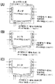
なお、上述したいずれの実施の形態においても、例えばボトムゲート型又はトップゲート型、デュアルゲート型MOSTFTを作製するに際し、図32(A)に概略的に示すように、段差4を設けるとこの上に成長する単結晶シリコン膜7が薄いために段切れ(接続不良)や細り(抵抗の増大)を生じることがあるので、ソース電極26(又はドレイン電極)との接続を確実に行うためには、図32(B)、(C)に示すように、その電極を段差4を含む領域上に被着することが望ましい。
【0199】
なお、図26の(7)の工程又は図29の(9)の工程において、単結晶シリコン層7上にトップゲート絶縁膜の形成後に、イオン注入、活性化処理し、その後にトップゲート電極、ソース、ドレイン電極をアルミニウムで同時に形成してよい。
【0200】
また、上記した段差4は、図33(A)に示すように、上述の例では基板1に(更にはその上のSiN等の膜にも)形成したが、例えば図33(B)に示すように、基板1上の結晶性サファイア膜50(これはガラス基板1からのイオンの拡散ストッパ機能がある。)に形成することもできる。この結晶性サファイア膜50の代わりに、或いはこの結晶性サファイア膜の下に上述したゲート絶縁膜72及び73を設け、これに段差4を形成してもよい。結晶性サファイア膜50に段差4を設けた例を図33(C)、(D)、(E)にそれぞれ例示した。
【0201】
<第7の実施の形態>
図34〜図36は、本発明の第7の実施の形態を示すものである。
【0202】
本実施の形態では、上述した段差4の外側に(即ち、段差以外の基板1上に)各TFTを形成した各種の例を示す。なお、単結晶シリコン層7やゲート/ソース/ドレイン電極26、27については簡略に図示している。
【0203】
まず、図34はトップゲート型TFTを示すが、(a)は段差による凹部4をソース側の一辺にソース領域に沿って形成し、この凹部以外の基板平坦面上において単結晶シリコン層7上にゲート絶縁膜12及びゲート電極11を形成している。同様に、(b)は、段差による凹部4をソース領域のみならずチャンネル長方向にドレイン領域端まで沿って2辺に亘ってL字パターンに形成した例、(c)は同様の凹部4をTFT能動領域を囲むように4辺に亘って矩形状に形成した例を示す。また、(d)は同様の凹部4を3辺に亘って形成した例、(e)は同様の凹部4を2辺に亘ってL字パターンに形成した例であるが、いずれも、隣接する凹部4−4間は連続していない。
【0204】
このように、各種パターンの凹部4を形成可能であると共に、TFTを凹部4以外の平坦面上に設けているので、TFTの作製が容易となる。
【0205】
図35は、ボトムゲート型MOSTFTの場合であるが、図34に示した各種パターンの段差(又は凹部)4を同様に形成することができる。即ち、図35(a)は図34(a)に対応した例であって、ボトムゲート型MOSTFTを段差による凹部4以外の平坦面上に形成したものである。同様に、図35(b)は図34(b)に、図35(c)は図34(c)や(d)に対応した例を示す。図35(d)は結晶性サファイア膜50に段差4を設けた場合である。
【0206】
図36は、デュアルゲート型MOSTFTの場合であるが、これも図34に示した各種パターンの段差(又は凹部)4を同様に形成することができ、例えば図34(c)に示した段差4の内側領域の平坦面上にデュアルゲート型MOSTFTを作製することができる。
【0207】
<第8の実施の形態>
図37〜図39は、本発明の第8の実施の形態を示すものである。
【0208】
図37の例は、自己整合型LDD構造のTFT、例えばトップゲート型LDD−TFTを複数個連ねたダブルゲート型MOSTFTに関するものである。
【0209】
これによれば、ゲート電極11を2つに分岐させ、一方を第1のゲートとして第1のLDD−TFT用、他方を第2のゲートとしての第2のLDD−TFT用として用いる(但し、単結晶シリコン層の中央部においてゲート電極間にN+ 型領域100を設け、低抵抗化を図っている)。この場合、各ゲートに異なる電圧を印加してもよいし、また何らかの原因で一方のゲートが動作不能になったとしても、残りのゲートを用いることによってソース/ドレイン間でのキャリアの移動を行え、信頼性の高いデバイスを提供できることになる。また、第1のLDD−TFTと第2のLDD−TFTとを直列に2個接続して各画素を駆動する薄膜トランジスタを形成するようにしたので、オフしているときに、各薄膜トランジスタのソース−ドレイン間に印加される電圧を大幅に減少させることができる。したがって、オフ時に流れるリーク電流を少なくすることができ、液晶ディスプレイのコントラスト及び画質を良好に改善することができる。また、上記LDDトランジスタにおける低濃度ドレイン領域と同じ半導体層のみを用いて上記2つのLDDトランジスタを接続するようにしているので、各トランジスタ間の接続距離を短くすることができ、LDDトランジスタを2個つなげても所要面積が大きくならないようにすることができる。なお、上記の第1、第2のゲートは互いに完全に分離し、独立して動作させることも可能である。
【0210】
図38の例は、ボトムゲート型MOSTFTをダブルゲート構造としたもの(A)と、デュアルゲート型MOSTFTをダブルゲート構造としたもの(B)である。
【0211】
これらのダブルゲート型MOSTFTも、上記のトップゲート型と同様の利点を有するが、このうちデュアルゲート型の場合は更に、上下のゲート部のいずれかが動作不能となっても一方のゲート部を使用できることも利点である。
【0212】
図39には、上記の各ダブルゲート型MOSTFTの等価回路図を示している。なお、上記においては、ゲートを2つに分岐したが、3つ又はそれ以上に分岐又は分割することもできる。これらのダブルゲート又はマルチゲート構造において、チャンネル領域内に2以上の分岐した同電位のゲート電極を有するか、又は分割された異電位又は同電位のゲート電極を有していてよい。
【0213】
<第9の実施の形態>
図40は、本発明の第9の実施の形態を示すものであって、nMOSTFTのデュアルゲート型構造のTFTにおいて、上下のゲート部のいずれか一方をトランジスタ動作させるが、他方のゲート部は次のように動作させている。
【0214】
即ち、図40(A)は、nMOSTFTにおいて、トップゲート側のゲート電極に常に任意の負電圧を印加してバックチャンネルのリーク電流を低減させるものである。トップゲート電極をオープンにする場合は、ボトムゲート型として使用するときである。また、図40(B)は、ボトムゲート側のゲート電極に常に任意の負電圧を印加してバックチャンネルのリーク電流を低減させるものである。この場合も、ボトムゲート電極をオープンにすると、トップゲート型として使用できる。なお、pMOSTFTの場合には、常に任意の正電圧をゲート電極に印加すれば、バックチャンネルのリーク電流を減らせる。
【0215】
いずれも、単結晶シリコン層7と絶縁膜との界面は結晶性が悪く、リーク電流が流れやすいが、上記のような電極の負電圧印加によってリーク電流を遮断できる。これは、LDD構造の効果と併せて、有利となる。また、ガラス基板1側から入射する光でリーク電流が流れることがあるが、ボトムゲート電極で光を遮断するので、リーク電流を低減できる。
【0216】
<第10の実施の形態>
図41〜図46は、本発明の第10の実施の形態を示すものである。
【0217】
本実施の形態は、基板には上述した如き段差(凹部)を設けず、基板の平坦面上に上述した物質層(例えば結晶性サファイア膜)を形成し、この物質層をシードとして単結晶シリコン層をヘテロエピタキシャル成長させ、これを用いてトップゲート型MOSTFTを構成したアクティブマトリクス反射型液晶表示装置(LCD)に関するものである。
【0218】
図41〜図46について、本実施の形態によるアクティブマトリクス反射型LCDをその製造工程に従って説明する。但し、図41〜図45において、各図の左側は表示部の製造工程、右側は周辺駆動回路部の製造工程を示す。
【0219】
まず、図41の(1)に示すように、石英ガラス、透明性結晶化ガラスなどの絶縁基板1の一主面において、少なくともTFT形成領域に、結晶性サファイア膜(厚さ20〜200nm)50を形成する。この結晶性サファイア膜50は、高密度プラズマCVD法や、触媒CVD法(特開昭63−40314号公報参照)等により、トリメチルアルミニウムガスなどを酸化性ガス(酸素・水分)で酸化し、結晶化させて作成する。絶縁基板1として高耐熱性ガラス基板(8〜12インチφ、700〜800μm厚)が使用可能である。
【0220】
次いで、図41の(2)に示すように、図1の(3)と同様に、結晶性サファイア膜50上の全面において、シリコンを約1重量%含有するシリコン・インジウム溶融液6を、900〜930℃に加熱された基板1上に塗布する。或いは、溶融液中に基板1をディッピングするか、或いは、溶融液表面を徐々に移動させてフローティングさせる方法や、噴流式、超音波作用下での接触方法も可能である。但し、シリコン・インジウム溶融液に代えてシリコン・インジウム・ガリウム又はシリコン・ガリウム融液も使用可能であるが、以下、シリコン・インジウム融液を代表例として説明する。
【0221】
次いで、基板1を数分〜数10分間保持した後、徐々に冷却する(ディッピングの場合は徐々に引き上げる)ことによって、インジウムに溶解していたシリコンは、結晶性サファイア膜50をシード(種)として図41の(3)に示すようにヘテロエピタキシャル成長し、厚さ例えば0.1μm程度のP型単結晶シリコン層7として析出する。ディッピング法及びフローティング法では、溶融液組成、温度、引き上げ速度などの管理が容易であり、エピタキシャル成長層の厚みやP型キャリア不純物濃度を容易にコントロールできる。
【0222】
上記のようにして堆積した単結晶シリコン層7は結晶性サファイア膜50が単結晶シリコンと良好な格子整合を示すために、例えば(100)面が基板上にヘテロエピタキシャル成長する。
【0223】
こうして、ヘテロエピタキシャル成長によって基板1上に単結晶シリコン層7を析出させた後、図42の(4)に示すように、表面のインジウム膜6Aを塩酸、硫酸などによって溶解除去し、更に上述したと同様にして、単結晶シリコン層7をチャンネル領域とするトップゲート型MOSTFTの作製を行う。
【0224】
まず、上記のヘテロエピタキシャル成長による単結晶シリコン層7の全面にP型キャリア不純物、例えばボロンイオンを適量ドーピングして比抵抗を調整する。また、pMOSTFT形成領域のみ、選択的にN型キャリア不純物をドーピングしてN型ウエルを形成する。例えば、pチャンネルTFT部をフォトレジスト(図示せず)でマスクし、P型不純物イオン(例えばB+ )を10kVで2.7×10¹¹atoms/cm2 のドーズ量でドーピングし、比抵抗を調整する。また、図42の(5)に示すように、pMOSTFT形成領域の不純物濃度制御のため、nMOSTFT部をフォトレジスト60でマスクし、N型不純物イオン(例えばP+ )65を10kVで1×10¹¹atoms/cm2 のドーズ量でドーピングし、N型ウエル7Aを形成する。
【0225】
次いで、図42の(6)に示すように、単結晶シリコン層7の全面上に、プラズマCVD、高密度プラズマCVD、触媒CVD法等でSiO2 (約200nm厚)とSiN(約100nm厚)をこの順に連続形成してゲート絶縁膜8を形成し、更に、モリブデン・タンタル(Mo・Ta)合金のスパッタ膜9(500〜600nm厚)を形成する。
【0226】
次いで、図42の(7)に示すように、汎用のフォトリソグラフィ技術により、表示領域のTFT部と、周辺駆動領域のTFT部とのそれぞれの段差領域(凹部内)にフォトレジストパターン10を形成し、連続したエッチングにより、(Mo・Ta)合金のゲート電極11とゲート絶縁膜(SiN/SiO2 )12とを形成し、単結晶シリコン層7を露出させる。(Mo・Ta)合金膜9は酸系エッチング液、SiNはCF4 ガスのプラズマエッチング、SiO2 はフッ酸系エッチング液で処理する。
【0227】
次いで、図43の(8)に示すように、周辺駆動領域のnMOS及びpMOSTFT全部と、表示領域のnMOSTFTのゲート部をフォトレジスト13でカバーし、露出したnMOSTFTのソース/ドレイン領域にリンイオン14を例えば20kVで5×1013atoms/cm2 のドーズ量でドーピング(イオン注入)して、N- 型層からなるLDD部15を自己整合的(セルフアライン)に形成する。
【0228】
次いで、図43の(9)に示すように、周辺駆動領域のpMOSTFT全部と、周辺駆動領域のnMOSTFTのゲート部と、表示領域のnMOSTFTのゲート及びLDD部とをフォトレジスト16でカバーし、露出した領域にリン又はひ素イオン17を例えば20kVで5×10¹⁵atoms/cm2 のドーズ量でドーピング(イオン注入)して、nMOSTFTのN+ 型層からなるソース部18及びドレイン部19とLDD部15とを形成する。
【0229】
次いで、図43の(10)に示すように、周辺駆動領域のnMOSTFT及び表示領域のnMOSTFTの全部とpMOSTFTのゲート部をフォトレジスト20でカバーし、露出した領域にボロンイオン21を例えば10kVで5×10¹⁵atoms/cm2 のドーズ量でドーピング(イオン注入)してpMOSTFTのP+ 層のソース部22及びドレイン部23を形成する。なお、この作業は、nMOS周辺駆動回路の場合はpMOSTFTが無いので、不要な作業である。
【0230】
次いで、図44の(11)に示すように、TFT、ダイオードなどの能動素子部や、抵抗、インダクタンスなどの受動素子部をアイランド化するため、フォトレジスト24を設け、周辺駆動領域及び表示領域のすべての能動素子部及び受動素子部以外の単結晶シリコン薄膜層を汎用フォトリソグラフィ及びエッチング技術で除去する。エッチング液はフッ酸系である。
【0231】
次いで、図44の(12)に示すように、プラズマCVD、高密度プラズマCVD、触媒CVD法等により、SiO2 膜(約200nm厚)及びリンシリケートガラス(PSG)膜(約300nm厚)をこの順に全面に連続形成して保護膜25を形成する。
【0232】
そして、この状態で単結晶シリコン層を活性化処理する。この活性化においてハロゲン等のランプアニール条件は約1000℃、約10秒程度であり、これに耐えるゲート電極材が必要であるが、高融点のMo・Ta合金は適している。このゲート電極材は従って、ゲート部のみならず配線として広範囲に亘って引き廻して設けることができる。なお、ここでは高価なエキシマレーザーアニールは使用しないが、仮に利用するとすれば、その条件はXeCl(308nm波長)で全面、又は能動素子部及び受動素子部のみの選択的な90%以上のオーバーラップスキャンニングが望ましい。
【0233】
次いで、図44の(13)に示すように、汎用フォトリソグラフィ及びエッチング技術により、周辺駆動回路の全TFTのソース/ドレイン部、及び表示用TFTのソース部のコンタクト用窓開けを行う。
【0234】
そして、全面に500〜600nm厚のアルミニウム又は1%Si入りアルミニウム等のスパッタ膜を形成し、汎用フォトリソグラフィ及びエッチング技術により、周辺駆動回路及び表示部のすべてのTFTのソース電極26と周辺駆動回路部のドレイン電極27を形成すると同時に、データライン及びゲートラインを形成する。その後に、フォーミングガス(N2 +H2 )中、約400℃/1hで、シンター処理する。
【0235】
次いで、図44の(14)に示すように、プラズマCVD、高密度プラズマCVD、触媒CVD法等により、PSG膜(約300nm厚)及びSiN膜(約300nm厚)からなる絶縁膜36を全面に形成する。次いで、表示用TFTのドレイン部のコンタクト用窓開けを行う。なお、画素部のSiO2 、PSG及びSiN膜は除去する必要はない。
【0236】
次いで、図6の(17)で述べたと同様の目的で、図45の(15)に示すように、全面に、スピンコート等で2〜3μm厚みの感光性樹脂膜28を形成し、図45の(16)に示すように、汎用フォトリソグラフィ及びエッチング技術により、少なくとも画素部に最適な反射特性と視野角特性を得るための凹凸形状パターンを形成し、リフローさせて凹凸粗面28Aからなる反射面下部を形成する。同時に表示用TFTのドレイン部のコンタクト用の樹脂窓開けを行う。
【0237】
次いで、図45の(17)に示すように、全面に400〜500nm厚のアルミニウム又は1%Si入りアルミニウム等のスパッタ膜を形成し、汎用フォトリソグラフィ及びエッチング技術により、画素部以外のアルミニウム膜等を除去し、表示用TFTのドレイン部19と接続した凹凸形状のアルミニウム等の反射部29を形成する。これは表示用の画素電極として用いられる。その後に、フォーミングガス中、約300℃/1hでシンター処理し、コンタクトを十分にする。尚、反射率を高めるために、アルミニウム系に代えて銀又は銀合金を使用してもよい。
【0238】
以上のようにして、結晶性サファイア膜50を高温ヘテロエピタキシャル成長のシードとして単結晶シリコン層7を形成し、この単結晶シリコン層7を用いた表示部及び周辺駆動回路部にそれぞれ、トップゲート型のnMOSLDD−TFT、pMOSTFT及びnMOSTFTで構成するCMOS回路を作り込んだ表示部−周辺駆動回路部一体型のアクティブマトリクス基板30を作製することができる。
【0239】
こうして得られたアクティブマトリクス基板(駆動基板)30を用いて、図6で述べたと同様にして図46の反射型液晶表示装置(LCD)を製造する。
【0240】
本実施の形態では、上述した第1の実施の形態で述べた優れた効果が得られることは明らかである。その上、基板1に段差を設けることなしに結晶性サファイア膜50のみによって単結晶シリコン層7をヘテロエピタキシャル成長させているので、段差の形成工程を省略し、より製造工程を簡略化できると共に、成長する単結晶シリコン層の段切れ等の問題も解消できることになる。
【0241】
<第11の実施の形態>
図47〜図49について、本発明の第11の実施の形態を説明する。
【0242】
本実施の形態は、上述の第10の実施の形態と比べて、同様のトップゲート型MOSTFTを表示部及び周辺駆動回路部に有するが、上述の第10の実施の形態とは異なって、透過型LCDに関するものである。即ち、図40の(1)から図44の(14)に示す工程までは同様であるが、その工程後に、図47の(15)に示すように、絶縁膜25、36に表示用TFTのドレイン部コンタクト用の窓開け19を行うと同時に、透過率向上のために画素開口部の不要なSiO2 、PSG及びSiN膜を除去する。
【0243】
次いで、図47の(16)に示すように、全面にスピンコート等で2〜3μm厚みの感光性アクリル系透明樹脂の平坦化膜28Bを形成し、汎用フォトリソグラフィにより、表示用TFTのドレイン側の透明樹脂28Bの窓開けを行い、所定条件で硬化させる。
【0244】
次いで、図47の(17)に示すように、全面に130〜150nm厚のITOスパッタ膜を形成し、汎用フォトリソグラフィ及びエッチング技術により、表示用TFTのドレイン部19とコンタクトしたITO透明電極41を形成する。そして、熱処理(フォーミングガス中、200〜250℃/1h)により、表示用TFTのドレインとITOのコンタクト抵抗の低減化とITO透明度の向上を図る。
【0245】
そして、図48に示すように、対向基板32と組み合わせ、上述の第8の実施の形態と同様にして透過型LCDを組み立てる。但し、TFT基板側にも偏光板を貼り合わせる。この透過型LCDでは、実線のように透過光が得られるが、一点鎖線のように対向基板32側からの透過光が得られるようにもできる。
【0246】
この透過型LCDの場合、次のようにしてオンチップカラーフィルタ(OCCF)構造とオンチップブラック(OCB)構造を作製することができる。
【0247】
即ち、図41の(1)〜図44の(13)までの工程は上記の工程に準じて行うが、その後、図49の(14)に示すように、PSG/SiO2 の絶縁膜25のドレイン部も窓開けしてドレイン電極用のアルミニウム埋込み層41Aを形成した後、SiN/PSGの絶縁膜36を形成する。
【0248】
次いで、図49の(15)に示すように、R、G、Bの各色を各セグメント毎に顔料分散したフォトレジスト61を所定厚さ(1〜1.5μm)で形成した後、図49の(16)に示すように、汎用フォトリソグラフィ技術で所定位置(各画素部)のみを残すパターニングで各カラーフィルタ層61(R)、61(G)、61(B)を形成する(オンチップカラーフィルタ構造)。この際、ドレイン部の窓開けも行う。なお、不透明なセラミック基板は使用できない。
【0249】
次いで、図49の(16)に示すように、表示用TFTのドレインに連通するコンタクトホールに、カラーフィルタ層上にかけてブラックマスク層となる遮光層43を金属のパターニングで形成する。例えば、スパッタ法により、モリブデンを200〜250nm厚で成膜し、表示用TFTを覆って遮光する所定の形状にパターニングする(オンチップブラック構造)。
【0250】
次いで、図49の(17)に示すように、透明樹脂の平坦化膜28Bを形成し、更にこの平坦化膜に設けたスルーホールにITO透明電極41を遮光層43に接続するように形成する。
【0251】
このように、表示アレイ部上に、カラーフィルタ61やブラックマスク43を作り込むことにより、液晶表示パネルの開口率を改善し、またバックライトも含めたディスプレイモジュールの低消費電力化が実現する。
【0252】
<第12の実施の形態>
図50〜図58は、本発明の第12の実施の形態を示すものである。
【0253】
本実施の形態では、周辺駆動回路部は上述した第10の実施の形態と同様のトップゲート型のpMOSTFTとnMOSTFTとからなるCMOS駆動回路で構成する。表示部は反射型ではあるが、TFTを各種ゲート構造のものとして、種々の組み合わせにしている。
【0254】
即ち、図50(A)は、上述した第10の実施の形態と同様のトップゲート型のnMOSLDD−TFTを表示部に設けているが、図50(B)に示す表示部にはボトムゲート型のnMOSLDD−TFT、図50(C)に示す表示部にはデュアルゲート型のnMOSLDD−TFTをそれぞれ設けている。これらのボトムゲート型、デュアルゲート型MOSTFTのいずれも、後述のように、周辺駆動回路部のトップゲート型MOSTFTと共通の工程で作製可能であるが、特にデュアルゲート型の場合には上下のゲート部によって駆動能力が向上し、高速スイッチングに適し、また上下のゲート部のいずれかを選択的に用いて場合に応じてトップゲート型又はボトムゲート型として動作させることもできる。
【0255】
なお、図50(B)のボトムゲート型MOSTFTにおいて、図中の71はMo・Ta等のゲート電極であり、72はSiN膜及び73はSiO2 膜であってゲート絶縁膜を形成し、このゲート絶縁膜上にはトップゲート型MOSTFTと同様の単結晶シリコン層を用いたチャンネル領域等が形成されている。また、図50(C)のデュアルゲート型MOSTFTにおいて、下部ゲート部はボトムゲート型MOSTFTと同様であるが、上部ゲート部は、ゲート絶縁膜73をSiO2 膜とSiN膜で形成し、この上に上部ゲート電極74を設けている。
【0256】
次に、上記のボトムゲート型MOSTFTの製造方法を図51〜図55で、上記のデュアルゲート型MOSTFTの製造方法を図56〜図58でそれぞれ説明する。なお、周辺駆動回路部のトップゲート型MOSTFTの製造方法は図41〜図45において述べたものと同じであるので、ここでは図示を省略している。
【0257】
表示部において、ボトムゲート型MOSTFTを製造するには、まず、図51の(1)に示すように、基板1上に、モリブデン/タンタル(Mo・Ta)合金のスパッタ膜71(500〜600nm厚)を形成する。
【0258】
次いで、図51の(2)に示すように、フォトレジスト70を所定パターンに形成し、これをマスクにしてMo・Ta膜71をテーパエッチングし、側端部71aが台形状に20〜45度でなだらかに傾斜したゲート電極71を形成する。
【0259】
次いで、図51の(3)に示すように、フォトレジスト70の除去後に、モリブデン・タンタル合金膜71を含む基板1上に、プラズマCVD法等により、SiN膜(約100nm厚)72とSiO2 膜(約200nm厚)73とを、この順に積層したゲート絶縁膜を形成する。
【0260】
次いで、図52の(4)に示すように、図41の(1)と同じ工程において、上述したと同様に絶縁基板1の一主面において、少なくともTFT形成領域に、結晶性サファイア膜(厚さ20〜200nm)50を形成する。
【0261】
次いで、図52の(5)に示すように、図41の(2)〜(3)と同じ工程において、上述したと同様に単結晶シリコンをヘテロエピタキシャル成長し、厚さ例えば0.1μm程度の単結晶シリコン層7として析出させる。この際、下地のゲート電極71の側端部71aはなだらかな傾斜面となっているので、この面上には、段差4によるヘテロエピタキシャル成長を阻害せず、段切れなしに単結晶シリコン層7が成長することになる。
【0262】
次いで、図52の(6)に示すように、図42の(5)〜(7)の工程を経た後、図43の(8)と同じ工程において、表示部のnMOSTFTのゲート部をフォトレジスト13でカバーし、露出したnMOSTFTのソース/ドレイン領域にリンイオン14をドーピング(イオン注入)して、N- 型層からなるLDD部15を自己整合的に形成する。このとき、ボトムゲート電極71の存在によって表面高低差(又はパターン)を認識し易く、フォトレジスト13の位置合わせ(マスク合わせ)を行い易く、アライメントずれが生じにくい。
【0263】
次いで、図53の(7)に示すように、図43の(9)と同じ工程において、nMOSTFTのゲート部及びLDD部をフォトレジスト16でカバーし、露出した領域にリン又はひ素イオン17をドーピング(イオン注入)して、nMOSTFTのN+ 型層からなるソース部18及びドレイン部19を形成する。
【0264】
次いで、図53の(8)に示すように、図43の(10)と同じ工程において、nMOSTFTの全部をフォトレジスト20でカバーし、ボロンイオン21をドーピング(イオン注入)して周辺駆動回路部のpMOSTFTのP+ 層のソース部及びドレイン部を形成する。
【0265】
次いで、図53の(9)に示すように、図44の(11)と同じ工程において、能動素子部と受動素子部をアイランド化するため、フォトレジスト24を設け、単結晶シリコン薄膜層を汎用フォトリソグラフィ及びエッチング技術で選択的に除去する。
【0266】
次いで、図53の(10)に示すように、図44の(12)と同じ工程において、プラズマCVD、高密度プラズマCVD、触媒CVD法等により、SiO2 膜53(約300nm厚)とリンシリケートガラス(PSG)膜54(約300nm厚)をこの順に全面に形成する。なお、SiO2 膜53とPSG膜54は上述した保護膜25に相当するものである。そして、この状態で単結晶シリコン膜を上述したと同様に活性化処理する。
【0267】
次いで、図54の(11)に示すように、図44の(13)と同じ工程において、汎用フォトリソグラフィ及びエッチング技術により、ソース部のコンタクト用窓開けを行う。そして、全面に400〜500nm厚のアルミニウム又は1%Si入りアルミニウム等のスパッタ膜を形成し、汎用フォトリソグラフィ及びエッチング技術により、TFTのソース電極26を形成すると同時に、データライン及びゲートラインを形成する。その後に、フォーミングガス中、約400℃/1hで、シンター処理する。
【0268】
次いで、図54の(12)に示すように、図44の(14)と同じ工程において、高密度プラズマCVD、触媒CVD法等により、PSG膜(約300nm厚)及びSiN膜(約300nm厚)からなる絶縁膜36を全面に形成し、表示用のTFTのドレイン部のコンタクト用窓開けを行う。
【0269】
次いで、図54の(13)に示すように、図45の(15)と同じ工程において、スピンコート等で2〜3μm厚みの感光性樹脂膜28を形成し、図54の(14)に示すように、汎用フォトリソグラフィ及びエッチング技術により、少なくとも画素部に最適な反射特性と視野角特性を得るような凹凸形状パターンを形成し、リフローさせて凹凸粗面28Aからなる反射面下部を形成する。同時に表示用TFTのドレイン部のコンタクト用の樹脂窓開けを行う。
【0270】
次いで、図54の(14)に示すように、図45の(17)と同じ工程において、全面に400〜500nm厚のアルミニウム又は1%Si入りアルミニウム等のスパッタ膜を形成し、汎用フォトリソグラフィ及びエッチング技術により、表示用TFTのドレイン部19と接続した凹凸形状のアルミニウム反射部29を形成する。
【0271】
以上のようにして、結晶性サファイア膜50を高温ヘテロエピタキシャル成長のシードとして形成された単結晶シリコン層7を用いた表示部にボトムゲート型のnMOSLDD−TFT(周辺部ではトップゲート型のpMOSTFT及びnMOSTFTからなるCMOS駆動回路)を作り込んだ表示部−周辺駆動回路部一体型のアクティブマトリクス基板30を作製することができる。
【0272】
図55は、表示部に設ける上記のボトムゲート型MOSTFTのゲート絶縁膜をMo・Taの陽極酸化法で形成した例を示す。
【0273】
即ち、図51の(2)の工程後に、図55の(3)に示すようにモリブデン・タンタル合金膜71を公知の陽極酸化処理することによって、その表面にTa2 O5 からなるゲート絶縁膜74を100〜200nm厚に形成する。
【0274】
この後の工程は、図55の(4)に示すように、図52の(4)〜(5)の工程と同様にして結晶性サファイア膜50を形成し、単結晶シリコン膜7をヘテロエピタキシャル成長した後、図52の(6)〜図54の(14)の工程と同様にして図55の(5)に示すように、アクティブマトリクス基板30を作製する。
【0275】
次に、表示部において、デュアルゲート型MOSTFTを製造するには、まず、図51の(1)〜図52の(5)までの工程は、上述したと同様に行う。
【0276】
即ち、図56の(6)に示すように、絶縁膜72、73上に結晶性サファイア膜50を形成し、更に、この結晶性サファイア膜50をシードとして単結晶シリコン層7をヘテロエピタキシャル成長させる。次いで、図42の(6)と同じ工程において、単結晶シリコン薄膜7上の全面に、プラズマCVD、触媒CVD等によりSiO2 膜(約200nm厚)とSiN膜(約100nm厚)をこの順に連続形成して絶縁膜80(これは上述の絶縁膜8に相当)を形成し、更に、Mo・Ta合金のスパッタ膜81(500〜600nm厚)(これは上述のスパッタ膜71に相当)を形成する。
【0277】
次いで、図56の(7)に示すように、図42の(7)と同じ工程において、フォトレジストパターン10を形成し、連続したエッチングによりMo・Ta合金のトップゲート電極82(これは上述のゲート電極12に相当)と、ゲート絶縁膜83(これは上述のゲート絶縁膜11に相当)を形成し、単結晶シリコン薄膜層7を露出させる。
【0278】
次いで、図56の(8)に示すように、図43の(8)と同じ工程において、nMOSTFTのトップゲート部をフォトレジスト13でカバーし、露出した表示用のnMOSTFTのソース/ドレイン領域にリンイオン14をドーピング(イオン注入)して、N- 型層のLDD部15を形成する。
【0279】
次いで、図56(9)に示すように、図43の(9)と同じ工程において、nMOSTFTのゲート部及びLDD部をフォトレジスト16でカバーし、露出した領域にリン又はひ素イオン17をドーピング(イオン注入)して、nMOSTFTのN+ 型層からなるソース部18及びドレイン部19を形成する。
【0280】
次いで、図57の(10)に示すように、図43の(10)と同じ工程において、pMOSTFTのゲート部をフォトレジスト20でカバーし、露出した領域にボロンイオン21をドーピング(イオン注入)して周辺駆動回路部のpMOSTFTのP+ 層のソース部及びドレイン部を形成する。
【0281】
次いで、図57の(11)に示すように、図44の(11)と同じ工程において、能動素子部と受動素子部をアイランド化するため、フォトレジスト24を設け、能動素子部と受動素子部以外の単結晶シリコン薄膜層を汎用フォトリソグラフィ及びエッチング技術で選択的に除去する。
【0282】
次いで、図57の(12)に示すように、図44の(12)と同じ工程において、プラズマCVD、高密度プラズマCVD、触媒CVD法等により、SiO2 膜53(約200nm厚)とリンシリケートガラス(PSG)膜54(約300nm厚)を全面に形成する。これらの膜53、54は上述の保護膜25に相当する。そして、単結晶シリコン層7を活性化処理する。
【0283】
次いで、図57の(13)に示すように、図44の(13)と同じ工程において、ソース部のコンタクト用窓開けを行う。そして、全面に400〜500nm厚のアルミニウム又は1%Si入りアルミニウム等のスパッタ膜を形成し、汎用フォトリソグラフィ及びエッチング技術により、ソース電極26を形成すると同時に、データライン及びゲートラインを形成する。
【0284】
次いで、図58の(14)に示すように、図44の(14)と同じ工程でPSG膜(約300nm厚)及びSiN膜(約300nm厚)からなる絶縁膜36を全面に形成し、表示用のTFTのドレイン部のコンタクト用窓開けを行う。
【0285】
次いで、図58の(15)に示すように、全面に、スピンコート等で2〜3μm厚みの感光性樹脂膜28を形成し、図58の(16)に示すように、図45の(16)、(17)の工程と同様に、少なくとも画素部に凹凸粗面28Aからなる反射面下部を形成し、同時に表示用TFTのドレイン部のコンタクト用の樹脂窓開けを行い、更に表示用TFTのドレイン部19と接続した、最適な反射特性と視野角特性を得るための凹凸形状のアルミニウム等の反射部29を形成する。
【0286】
以上のようにして、結晶性サファイア膜50をヘテロエピタキシャル成長のシードとして形成された単結晶シリコン層7を用い、表示部にデュアルゲート型のnMOSLDDTFTを、周辺駆動回路部にトップゲート型のpMOSTFT及びnMOSTFTからなるCMOS駆動回路を作り込んだ表示部−周辺駆動回路部一体型のアクティブマトリクス基板30を作製することができる。
【0287】
<第13の実施の形態>
図59〜図61は、本発明の第13の実施の形態を示すものである。
【0288】
本実施の形態では、上述した実施の形態とは異なり、トップゲート部のゲート電極をアルミニウム等の比較的耐熱性の低い材料で形成している。
【0289】
まず、表示部及び周辺駆動回路部共にトップゲート型MOSTFTを設ける場合には、上述した第10の実施の形態における図41の(1)〜図42の(5)までの工程は同様に行って、図59の(5)に示すように、周辺駆動回路部のpMOSTFT部にN型ウエル7Aを形成する。
【0290】
次いで、図59の(6)に示すように、周辺駆動領域のnMOS及びpMOSTFT全部と、表示領域のnMOSTFTのゲート部をフォトレジスト13でカバーし、露出したnMOSTFTのソース/ドレイン領域にリンイオン14を例えば20kVで5×1013atoms/cm2 のドーズ量でドーピング(イオン注入)して、N- 型層からなるLDD部15を自己整合的に形成する。
【0291】
次いで、図60の(7)に示すように、周辺駆動領域のpMOSTFT全部と、周辺駆動領域のnMOSTFTのゲート部と、表示領域のnMOSTFTのゲート及びLDD部とをフォトレジスト16でカバーし、露出した領域にリン又はひ素イオン17を例えば20kVで5×10¹⁵atoms/cm2 のドーズ量でドーピング(イオン注入)して、nMOSTFTのN+ 型層からなるソース部18及びドレイン部19とLDD部15とを形成する。この場合、仮想線のようにレジスト13を残し、これを覆うようにレジスト16を設ければ、レジスト16形成時のマスクの位置合せをレジスト13を目安にでき、マスク合せが容易となり、アライメントずれも少なくなる。
【0292】
次いで、図60の(8)に示すように、周辺駆動領域のnMOSTFT及び表示領域のnMOSTFTの全部とpMOSTFTのゲート部をフォトレジスト20でカバーし、露出した領域にボロンイオン21を例えば10kVで5×10¹⁵atoms/cm2 のドーズ量でドーピング(イオン注入)してpMOSTFTのP+ 層のソース部22及びドレイン部23を形成する。
【0293】
次いで、レジスト20の除去後に、図60の(9)に示すように、単結晶シリコン層7、7Aを上述したと同様に活性化処理し、更に表面にゲート絶縁膜12、ゲート電極材料(アルミニウム又は1%Si入りアルミニウム等)11を形成する。ゲート電極材料層11は真空蒸着法又はスパッタ法で形成可能である。
【0294】
次いで、上述したと同様に、各ゲート部をパターニングした後、能動素子部と受動素子部をアイランド化し、更に図61の(10)に示すように、SiO2 膜(約200nm厚)及びリンシリケートガラス(PSG)膜(約300nm厚)をこの順に全面に連続形成して保護膜25を形成する。
【0295】
次いで、図61の(11)に示すように、汎用フォトリソグラフィ及びエッチング技術により、周辺駆動回路の全TFTのソース/ドレイン部、及び表示用TFTのソース部のコンタクト用窓開けを行う。
【0296】
そして、全面に500〜600nm厚のアルミニウム等のスパッタ膜を形成し、汎用フォトリソグラフィ及びエッチング技術により、周辺駆動回路及び表示部のすべてのTFTのソース電極26と周辺駆動回路部のドレイン電極27を形成すると同時に、データライン及びゲートラインを形成する。その後に、フォーミングガス(N2 +H2 )中、約400℃/1hで、シンター処理する。
【0297】
次いで、図44の(14)〜図45の(17)と同様にして単結晶シリコン層7を用いた表示部及び周辺駆動回路部にそれぞれ、アルミニウム又は1%Si入りアルミニウム等をゲート電極とするトップゲート型のnMOSLDD−TFT、pMOSTFT及びnMOSTFTで構成するCMOS駆動回路を作り込んだ表示部−周辺駆動回路部一体型のアクティブマトリクス基板30を作製することができる。
【0298】
本実施の形態では、単結晶シリコン層7の活性化処理後にアルミニウム又はアルミニウム合金等のゲート電極11を形成しているので、その活性化処理時の熱の影響はゲート電極材料の耐熱性とは無関係となるため、トップゲート電極材料として比較的耐熱性が低く、低コストのアルミニウム等でも使用可能となり、電極材料の選択の幅も広がる。これは、表示部がボトムゲート型MOSTFTの場合も同様である。
【0299】
次に、表示部にデュアルゲート型MOSTFT、周辺駆動回路にトップゲート型MOSTFTを設ける場合には、上述した第6の実施の形態における図29の(8)〜図31の(15)で述べた工程と同様に行って、表示部及び周辺駆動回路部にそれぞれ、アルミニウム等をゲート電極とするデュアルゲート型のnMOSLDD−TFT、トップゲート型pMOSTFT及びnMOSTFTで構成するCMOS駆動回路を作り込んだ表示部−周辺駆動回路部一体型のアクティブマトリクス基板30を作製することができる。
【0300】
<第14の実施の形態>
図62〜図63は、本発明の第14の実施の形態を示すものである。
【0301】
図62の例は、上述の第12の実施の形態において、自己整合型LDD構造のTFT、例えばトップゲート型LDD−TFTを複数個連ねたダブルゲート型MOSTFTに関するものである。
【0302】
図63の例は、ボトムゲート型MOSTFTをダブルゲート構造としたもの(A)と、デュアルゲート型MOSTFTをダブルゲート構造としたもの(B)である。
【0303】
これらのダブルゲート型MOSTFTも、上述した図37〜図38で述べたと同様の利点を有する。
【0304】
<第15の実施の形態>
図64〜図72は、本発明の第15の実施の形態を示すものである。
【0305】
上述したように、トップゲート型、ボトムゲート型、デュアルゲート型の各TFTはそれぞれ構造上、機能上の差異又は特長があることから、これらを表示部と周辺駆動回路部において採用する際に、これら各部間でTFTを種々に組み合わせて設けることが有利なことがある。
【0306】
例えば、図64に示すように、表示部にトップゲート型、ボトムゲート型、デュアルゲート型のいずれかのMOSTFTを採用した場合、周辺駆動回路にはトップゲート型MOSTFT、ボトムゲート型MOSTFT、デュアルゲート型MOSTFTのうち、少なくともトップゲート型を採用するか、或いはそれらが混在することも可能である。この組み合わせは12通り(No.1〜No.12)挙げられる。特に、周辺駆動回路のMOSTFTにデュアルゲート構造を用いると、このようなデュアルゲート構造は、上下のゲート部の選択によってトップゲート型にもボトムゲート型にも容易に変更することができ、また、周辺駆動回路の一部に大きな駆動能力のTFTが必要な場合は、デュアルゲート型が必要となる場合もある。例えば、LCD以外の電気光学装置として本発明を有機ELやFED等に適用する場合は必要であると考えられる。
【0307】
図65及び図66は表示部のMOSTFTがLDD構造でないとき、図67及び図68は表示部のMOSTFTがLDD構造であるとき、図69及び図70は周辺駆動回路部のMOSTFTがLDD構造のTFTを含むとき、図71及び図72は周辺駆動回路部と表示部の双方がLDD構造のMOSTFTを含むときのそれぞれにおいて、周辺駆動回路部と表示部の各MOSTFTの組み合わせをチャンネル導電型別に示した各種の例(No.1〜No.216)を示す。
【0308】
このように、図64に示したゲート構造別の組み合わせは、具体的には図65〜図72に示したようになる。これは、周辺駆動回路部がトップゲート型と他のゲート型との混在したMOSTFTからなっている場合も、同様の組み合わせが可能である。なお、図64〜図72に示したTFTの各種組合せは、TFTのチャンネル領域などを単結晶シリコンで形成する場合に限らず、多結晶シリコンやアモルファスシリコン(但し、表示部のみ)で形成する場合も同様に適用可能である。
【0309】
<第16の実施の形態>
図73〜図74は、本発明の第16の実施の形態を示すものである。
【0310】
本実施の形態では、アクティブマトリクス駆動LCDにおいて、周辺駆動回路部は、駆動能力の向上の点から、本発明に基づいて上述の単結晶シリコン層を用いたTFTを設ける。但し、これはトップゲート型に限らず、他のゲート型が混在してよいし、チャンネル導電型も種々であってもよく、また単結晶シリコン層以外の多結晶シリコン層を用いたMOSTFTが含まれていてもよい。これに対し、表示部のMOSTFTは、単結晶シリコン層を用いるのが望ましいが、これに限らず、多結晶シリコンやアモルファスシリコン層を用いたものであってよく、或いは3種のシリコン層の少なくとも2種が混在したものであってもよい。但し、表示部をnMOSTFTで形成するときは、アモルファスシリコン層を用いても実用的なスイッチング速度は得られるが、単結晶シリコン又は多結晶シリコン層の方がTFT面積を小さくでき、画素欠陥の減少の面でもアモルファスシリコンよりは有利である。なお、既述したヘテロエピタキシャル成長時に単結晶シリコンだけでなく、多結晶シリコンも同時に生じ、いわゆるCGS(Continuous grain silicon)構造も含まれることもあるが、これも能動素子と受動素子の形成に利用できる。
【0311】
図73には、各部間でのMOSTFTの各種組み合わせ例(A)、(B)、(C)を示し、図74にはその具体例を例示した。単結晶シリコンを用いると、電流駆動能力が向上するため、素子を小さくでき、大画面化が可能となり、表示部では開口率が向上する。
【0312】
なお、周辺駆動回路部では、上記のMOSTFTだけでなく、ダイオード、キャパシタンス、抵抗、インダクタンス等を集積した電子回路が絶縁基板(ガラス基板等)に一体形成されてよいことは勿論である。
【0313】
<第17の実施の形態>
図75は、本発明の第17の実施の形態を示すものである。
【0314】
本実施の形態は、上述した各実施の形態がアクティブマトリクス駆動の例についてのものであるのに対し、本発明をパッシブマトリクス駆動に適用したものである。
【0315】
即ち、表示部は、上述したMOSTFTの如きスイッチング素子を設けず、対向する基板に形成した一対の電極間に印加する電圧による電位差でのみ表示部の入射光又は反射光が調光される。こうした調光素子には、反射型、透過型のLCDをはじめ、有機又は無機EL(エレクトロルミネセンス表示素子)、FED(電界放出型表示素子)、LEPD(発光ポリマー表示素子)、LED(発光ダイオード表示素子)なども含まれる。
【0316】
<第18の実施の形態>
図76は、本発明の第18の実施の形態を示すものである。
【0317】
本実施の形態は、本発明をLCD以外の電気光学装置である有機又は無機EL(エレクトロルミネセンス)素子やFED(電界放出型表示素子)、LEPD(発光ポリマー表示素子)、LED(発光ダイオード表示素子)などに適用したものである。
【0318】
即ち、図76(A)には、アクティブマトリクス駆動のEL素子を示し、例えばアモルファス有機化合物を用いた有機EL層(又はZnS:Mnを用いた無機EL層)90を基板1上に設け、その下部に既述した透明電極(ITO)41を形成し、上部に陰極91を形成し、これら両極間の電圧印加によって所定色の発光がフィルタ61を通して得られる。
【0319】
この際、アクティブマトリクス駆動により透明電極41へデータ電圧を印加するために、基板1上の結晶性サファイア膜50(更には段差4)をシードとしてヘテロエピタキシャル成長させた単結晶シリコン層を用いた本発明による単結晶シリコンMOSTFT(即ち、nMOSLDD−TFT)が基板1上に作り込まれている。同様のTFTは周辺駆動回路にも設けられる。このEL素子は、単結晶シリコン層を用いたMOSLDD−TFTで駆動しているので、スイッチング速度が早く、またリーク電流も少ない。なお、上記のフィルタ61は、EL層90が特定色を発光するものであれば、省略可能である。
【0320】
なお、EL素子の場合、駆動電圧が高いため、周辺駆動回路部には、上記のMOSTFT以外に、高耐圧のドライバ素子(高耐圧cMOSTFTとバイポーラ素子など)を設けるのが有利である。
【0321】
図76(B)は、パッシブマトリクス駆動のFEDを示すが、対向するガラス基板1−32間の真空部において、両電極92−93間の印加電圧によって冷陰極94から放出された電子をゲートライン95の選択によって対向する螢光体層96へ入射させ、所定色の発光を得るものである。
【0322】
ここで、エミッタライン92は、周辺駆動回路へ導かれ、データ電圧で駆動されるが、その周辺駆動回路には、本発明に基づいて単結晶シリコン層を用いたMOSTFTが設けられ、エミッタライン92の高速駆動に寄与している。なお、このFEDは、各画素に上記のMOSTFTを接続することにより、アクティブマトリクス駆動させることも可能である。
【0323】
なお、図76(A)の素子において、EL層90の代わりに公知の発光ポリマーを用いれば、パッシブマトリクス又はアクティブマトリクス駆動の発光ポリマー表示装置(LEPD)として構成することができる。その他、図76(B)の素子において、ダイアモンド薄膜をカソード側に用いたFEDと類似のデバイスも構成できる。また、発光ダイオードにおいて、発光部に本発明によりエピタキシャル成長させた単結晶シリコンのMOSTFTにより、例えばガリウム系(ガリウム・アルミニウム・ひ素など)の膜からなる発光部を駆動できる。或いは、本発明のエピタキシャル成長法で発光部の膜を単結晶成長させることも考えられる。
【0324】
以上に述べた本発明の実施の形態は、本発明の技術的思想に基いて種々変形が可能である。
【0325】
例えば、上述した低融点金属の溶融液6の塗布時に、溶解度が大きい3族又は5族元素を、例えばボロン、リン、アンチモン、ひ素、アルミニウム、ガリウム、インジウム、ビスマスなどを多結晶シリコン又はアモルファスシリコン膜5に適量ドープしておけば、成長するシリコンエピタキシャル成長層7のP型又はN型のチャンネル導電型や、そのキャリア濃度を任意に制御することができる。
【0326】
また、ガラス基板からのイオンの拡散防止のために基板表面にSiN膜(例えば50〜200nm厚)、更には必要に応じてSiO2 膜(例えば100nm厚)を設けてよく、またこれらの膜に既述した如き段差4を形成してもよい。上述した段差はRIE以外にもイオンミリング法などによっても形成可能である。また、上述したように、段差4を基板1に形成する以外にも、結晶性サファイア膜又はサファイア基板自体の厚み内に段差4を形成してもよいことは勿論である。
【0327】
また、上述したサファイア(Al2 O3 )に代えて、単結晶シリコンと格子整合の良好なスピネル構造体(例えばマグネシアスピネル)(MgO・Al2 O3 )や、CaF2 、SrF2 、BaF2 、BP、(Y2 O3 )m 、(ZrO2 )1 -m等が使用可能である。
【0328】
また、本発明は周辺駆動回路のTFTに好適なものであるが、それ以外にもダイオードなどの素子の能動領域や、抵抗、キャパシタンス、インダクタンスなどの受動領域を本発明による単結晶シリコン層で形成することも可能である。
【0329】
【発明の作用効果】
本発明によれば、特に単結晶シリコンと格子整合の良い上記物質層(例えば結晶性サファイア膜)をシードにして、シリコン等を溶解した低融点金属の溶融液から、ヘテロエピタキシャル成長で単結晶シリコン層などの単結晶半導体層を形成し、このエピタキシャル成長層をアクティブマトリクス基板などの駆動基板の周辺駆動回路のトップゲート型MOSTFTや表示部−周辺駆動回路一体型のLCDなどの電気光学装置の周辺駆動回路のトップゲート型MOSTFTなどの能動素子や、抵抗、インダクタンス、キャパシタンス等の受動素子のうちの少なくとも能動素子に用いているので、次の(A)〜(G)に示す顕著な作用効果を得ることができる。
【0330】
(A)単結晶シリコンと格子整合の良い物質層(例えば結晶性サファイア膜)を基板上に形成し、その物質層をシードとしてヘテロエピタキシャル成長させることにより、540cm2 /v・sec以上の高い電子移動度の単結晶シリコン層の如き単結晶半導体層が得られるので、高性能ドライバ内蔵の表示用薄膜半導体装置などの電気光学装置の製造が可能となる。
【0331】
(B)特にこの単結晶シリコン層による単結晶シリコントップゲート型TFTは、高いスイッチング特性を有し、LDD構造を有するnMOS又はpMOS又はcMOSTFTの表示部と、高い駆動能力のcMOS、又はnMOS又はpMOSTFT又はこれらの混在からなる周辺駆動回路とを一体化した構成が可能となり、高画質、高精細、狭額縁、高効率、大画面の表示パネルが実現する。
【0332】
(C)そして、上記した物質層をヘテロエピタキシャル成長のシードとして用い、かつこの物質層上において、上記した低融点金属の溶融液を低温(例えば350℃)で調製し、それより少し高いだけの温度に加熱した基板上に塗布などの方法で形成できるから、比較的低温(例えば300〜400℃)でシリコン単結晶膜を均一に形成することができる。
【0333】
(D)固相成長法の場合のような中温で長時間(約600℃、十数時間)のアニールや、エキシマレーザーアニールが不要となるから、生産性が高く、高価な製造設備が不要でコストダウンが可能となる。
【0334】
(E)このヘテロエピタキシャル成長では、結晶性サファイア膜等の物質層の結晶性、溶融液の組成比、溶融液温度、基板の加熱温度、冷却速度等の調整により広範囲のP型不純物濃度と高移動度の単結晶シリコン薄膜が容易に得られるので、Vth(しきい値)調整が容易であり、低抵抗化による高速動作が可能である。
【0335】
(F)また、シリコン含有低融点金属溶融液層に、3族又は5族の不純物元素(ボロン、リン、アンチモン、ひ素、ビスマス、アルミニウムなど)を別途適量ドープしておけば、ヘテロエピタキシャル成長による単結晶シリコン薄膜の不純物種及び/又はその濃度、即ちP型/N型等の導電型及び/又はキャリア濃度を任意に制御することができる。
【0336】
(G)結晶性サファイア膜などの上記物質層は、様々な原子の拡散バリアになるため、ガラス基板からの不純物の拡散を抑制することができる。
【図面の簡単な説明】
【図1】本発明の第1の実施の形態によるLCD(液晶表示装置)の製造プロセスを工程順に示す断面図である。
【図2】同、LCDの製造プロセスを工程順に示す断面図である。
【図3】同、LCDの製造プロセスを工程順に示す断面図である。
【図4】同、LCDの製造プロセスを工程順に示す断面図である。
【図5】同、LCDの製造プロセスを工程順に示す断面図である。
【図6】同、LCDの製造プロセスを工程順に示す断面図である。
【図7】同、LCDの要部断面図である。
【図8】非晶質基板上のシリコン結晶成長の状況を説明するための概略斜視図である。
【図9】グラフォエピタキシャル成長技術における各種段差形状とシリコン成長結晶方位を示す概略断面図である。
【図10】Si−In状態図(A)及びSi−Ga状態図(B)である。
【図11】本発明の第1の実施の形態によるLCDの全体の概略レイアウトを示す斜視図である。
【図12】同、LCDの等価回路図である。
【図13】同、LCDの概略構成図である。
【図14】本発明の第2の実施の形態によるLCDの製造プロセスを工程順に示す断面図である。
【図15】同、LCDの要部断面図である。
【図16】同、LCDの製造プロセスを工程順に示す断面図である。
【図17】本発明の第5の実施の形態によるLCDの要部断面図である。
【図18】同、LCDの製造プロセスを工程順に示す断面図である。
【図19】同、LCDの製造プロセスを工程順に示す断面図である。
【図20】同、LCDの製造プロセスを工程順に示す断面図である。
【図21】同、LCDの製造プロセスを工程順に示す断面図である。
【図22】同、LCDの製造プロセスを工程順に示す断面図である。
【図23】同、LCDの製造プロセスを工程順に示す断面図である。
【図24】同、LCDの製造プロセスを工程順に示す断面図である。
【図25】同、LCDの製造プロセスを工程順に示す断面図である。
【図26】本発明の第6の実施の形態によるLCDの製造プロセスを工程順に示す断面図である。
【図27】同、LCDの製造プロセスを工程順に示す断面図である。
【図28】同、LCDの製造プロセスを工程順に示す断面図である。
【図29】同、LCDの製造プロセスを工程順に示す断面図である。
【図30】同、LCDの製造プロセスを工程順に示す断面図である。
【図31】同、LCDの製造プロセスを工程順に示す断面図である。
【図32】同、LCDの製造時の要部断面図である。
【図33】同、LCDの製造時の要部断面図である。
【図34】本発明の第7の実施の形態によるLCDの各種TFTを示す平面図又は断面図である。
【図35】同、LCDの製造時の各種TFTを示す断面図である。
【図36】同、LCDの要部断面図である。
【図37】本発明の第8の実施の形態によるLCDの要部断面図又は平面図である。
【図38】同、LCDの各種TFTの要部断面図である。
【図39】同、LCDのTFTの等価回路図である。
【図40】本発明の第9の実施の形態によるLCDのTFTの要部断面図である。
【図41】本発明の第10の実施の形態によるLCDの製造プロセスを工程順に示す断面図である。
【図42】同、LCDの製造プロセスを工程順に示す断面図である。
【図43】同、LCDの製造プロセスを工程順に示す断面図である。
【図44】同、LCDの製造プロセスを工程順に示す断面図である。
【図45】同、LCDの製造プロセスを工程順に示す断面図である。
【図46】同、LCDの要部断面図である。
【図47】本発明の第11の実施の形態によるLCDの製造プロセスを工程順に示す断面図である。
【図48】同、LCDの要部断面図である。
【図49】同、LCDの製造プロセスを工程順に示す断面図である。
【図50】本発明の第12の実施の形態によるLCDの要部断面図である。
【図51】同、LCDの製造プロセスを工程順に示す断面図である。
【図52】同、LCDの製造プロセスを工程順に示す断面図である。
【図53】同、LCDの製造プロセスを工程順に示す断面図である。
【図54】同、LCDの製造プロセスを工程順に示す断面図である。
【図55】同、LCDの製造プロセスを工程順に示す断面図である。
【図56】同、LCDの製造プロセスを工程順に示す断面図である。
【図57】同、LCDの製造プロセスを工程順に示す断面図である。
【図58】同、LCDの製造プロセスを工程順に示す断面図である。
【図59】本発明の第13の実施の形態によるLCDの製造プロセスを工程順に示す断面図である。
【図60】同、LCDの製造プロセスを工程順に示す断面図である。
【図61】同、LCDの製造プロセスを工程順に示す断面図である。
【図62】本発明の第14の実施の形態によるLCDの要部断面図又は平面図である。
【図63】同、LCDの各種TFTの要部断面図である。
【図64】本発明の第15の実施の形態によるLCDの各部TFTの組み合せを示す図である。
【図65】同、LCDの各部TFTの組み合せを示す図である。
【図66】同、LCDの各部TFTの組み合せを示す図である。
【図67】同、LCDの各部TFTの組み合せを示す図である。
【図68】同、LCDの各部TFTの組み合せを示す図である。
【図69】同、LCDの各部TFTの組み合せを示す図である。
【図70】同、LCDの各部TFTの組み合せを示す図である。
【図71】同、LCDの各部TFTの組み合せを示す図である。
【図72】同、LCDの各部TFTの組み合せを示す図である。
【図73】本発明の第16の実施の形態によるLCDの概略レイアウト図である。
【図74】同、LCDの各部TFTの組み合わせを示す図である。
【図75】本発明の第17の実施例によるデバイスの概略レイアウト図である。
【図76】本発明の第18の実施の形態によるEL及びFEDの要部断面図である。
【符号の説明】
1…ガラス(又は石英)基板、4…段差、7…単結晶シリコン層、
9…Mo・Ta層、11…ゲート電極、12…ゲート酸化膜、
14、17…N型不純物イオン、15…LDD部、
18、19…N+ 型ソース又はドレイン領域、21…P型不純物イオン、
22、23…P+ 型ソース又はドレイン領域、25、36…絶縁膜、
26、27、31、41…電極、28…平坦化膜、28A…粗面(凹凸)、
29…反射膜(又は電極)、30…LCD(TFT)基板、
33、34…配向膜、35…液晶、37、46…カラーフィルタ層、
43…ブラックマスク層、50…結晶性サファイア膜[0001]
BACKGROUND OF THE INVENTION
The present invention relates to a method of manufacturing an electro-optical device and a method of manufacturing a driving substrate for an electro-optical device, and more particularly, a top-gate thin-film insulating gate type electric field using a single crystal silicon layer heteroepitaxially grown on an insulating substrate as an active region. The present invention relates to a method suitable for a liquid crystal display device having an effect transistor (hereinafter referred to as a top gate type MOSTFT. The top gate type includes a stagger type and a coplanar type) and a passive region.
[0002]
[Prior art]
As an active matrix type liquid crystal display device, a display unit using amorphous silicon as a TFT and an IC for an external drive circuit, or a display unit and a drive circuit using polycrystalline silicon by a solid phase growth method as a TFT Are known (Japanese Patent Laid-Open No. 6-242433), an integrated type of a display unit and a drive circuit using polycrystalline silicon subjected to excimer laser annealing in a TFT (Japanese Patent Laid-Open No. 7-13030), and the like. Yes.
[0003]
[Problems to be solved by the invention]
However, the above-described conventional amorphous silicon TFT has good productivity, but the electron mobility is 0.5 to 1.0 cm. 2 Since it is as low as around / v · sec, a p-channel MOSTFT (hereinafter referred to as pMOSTFT) cannot be formed. Accordingly, since the peripheral driving unit using the pMOS TFT cannot be formed on the same glass substrate as the display unit, the driver IC is externally mounted and mounted by the TAB method, so that it is difficult to reduce the cost. For this reason, there is a limit to high definition. Furthermore, the electron mobility is 0.5 to 1.0 cm. 2 Since it is as low as around / v · sec, sufficient on-current cannot be obtained, and when used in a display portion, the transistor size inevitably increases, which is disadvantageous for the high aperture ratio of the pixel.
[0004]
The electron mobility of the conventional polycrystalline silicon TFT described above is 70 to 100 cm. 2 Since it can cope with high definition at / v · sec, LCD (Liquid Crystal Display) using a driver-integrated polycrystalline silicon TFT has recently attracted attention. However, in the case of a large LCD of 15 inches or more, the electron mobility of polycrystalline silicon is 70-100 cm. 2 Since / v · sec, the drive capability is insufficient, and eventually an external drive circuit IC is required.
[0005]
In a TFT using polycrystalline silicon formed by solid phase growth, a gate SiO is formed by annealing at 600 ° C. or more for several tens of hours and thermal oxidation at about 1000 ° C. 2 Therefore, it is necessary to employ a semiconductor manufacturing apparatus. Therefore, the wafer size of 8 to 12 inches φ is the limit, and it is necessary to employ high heat-resistant and expensive quartz glass, and it is difficult to reduce the cost. Therefore, it is limited to EVF and data / AV projector applications.
[0006]
Furthermore, in the conventional polycrystalline silicon TFT by excimer laser annealing described above, there are a number of problems such as excimer laser output stability, productivity, increase in device price due to increase in size, and yield / quality deterioration.
[0007]
In particular, when a large glass substrate of 1 m square or the like is used, the above-mentioned problems are expanded, and it is difficult to improve performance / quality and reduce costs.
[0008]
An object of the present invention is to form an active matrix substrate with a built-in high-performance driver by forming a single crystal silicon layer having a high electron / hole mobility at a relatively low temperature and uniformly, particularly in the peripheral drive circuit portion. An electro-optical device such as a thin film semiconductor device for display used can be manufactured, and an n-channel MOS TFT (hereinafter referred to as an nMOS TFT) or an LDMOS TFT having an LDD structure (Lightly doped drain structure) having high switching characteristics and low leakage current. Alternatively, a configuration in which a display unit of a complementary thin film insulated gate field effect transistor (hereinafter referred to as cMOSTFT) with high driving capability and a peripheral driving circuit made of this cMOSTFT, nMOSTFT, pMOSTFT, or a mixture thereof is possible. Realize high-quality, high-definition, narrow frame, high-efficiency, large-screen display panels Can be used even for large glass substrates with a relatively low strain point, high productivity, no need for expensive manufacturing equipment, cost reduction, and easy threshold adjustment Therefore, it is to enable high speed operation and large screen by reducing resistance.
[0009]
[Means for Solving the Problems]
That is, according to the present invention, a display unit in which pixel electrodes (for example, a plurality of pixel electrodes arranged in a matrix: the same applies hereinafter) and a peripheral drive circuit unit disposed in the periphery of the display unit are provided in a first manner. A predetermined optical material such as a liquid crystal between the first substrate and the second substrate (i.e., the same applies hereinafter) between the first substrate and the second substrate (i.e., the same applies hereinafter). In each of the manufacturing methods of the electro-optical device and the driving substrate for the electro-optical device,
On the one surface of the first substrate, a material layer, which will be described later, has a lattice match with single crystal silicon.
Forming a step;
A low-melting-point metal melt described later containing silicon on the first substrate including the material layer
Forming a layer;
Next, the molten liquid layer is subjected to a cooling treatment (preferably a slow cooling treatment). silicon The above
Heteroepitaxial growth using material layer as seed to deposit single crystal silicon layer
Process,
This single crystal silicon At least one of active and passive elements by applying a predetermined treatment to the layer
The step of forming an active element (for example, after the single crystal silicon layer is deposited, this single crystal silicon
A predetermined process is performed on the con layer to form a channel region, a source region, and a drain region.
And a gate portion comprising a gate insulating film and a gate electrode on the channel region,
Furthermore, source and drain electrodes are formed, and at least a part of the peripheral drive circuit section is configured.
The top gate type first thin film transistor (especially MOSTFT: hereinafter the same) to be formed
A process of forming as an active element, or a resistor, a capacitance, an inductor
Forming a passive element such as a
The present invention relates to an electro-optical device and a method of manufacturing a drive substrate for the electro-optical device. In the present invention, the active element is a concept including an element such as a thin film transistor and other diodes, and the passive element is a concept including a resistor (hereinafter the same). Typical examples of the thin film transistor include a field effect transistor (FET) (which can be either a MOS type or a junction type), and a bipolar transistor, but the present invention is applicable to any transistor. Yes (hereinafter the same). The passive element is a concept including resistance, inductance, capacitance, and the like. For example, a high dielectric film such as silicon nitride (hereinafter referred to as SiN) is sandwiched between the single crystal silicon layers (electrodes) whose resistance is reduced. There is a capacitance formed by
[0010]
According to the present invention, a single-crystal silicon thin film is obtained by heteroepitaxial growth from a low-melting-point metal melt in which silicon or the like is dissolved using the above material layer (for example, a crystalline sapphire film) having a good lattice match with single-crystal silicon as a seed. A single crystal semiconductor thin film is formed, and this epitaxial growth layer is used as a peripheral drive circuit for an electro-optical device such as a top gate MOSTFT of a peripheral drive circuit of a drive substrate such as an active matrix substrate or an LCD integrated with a display-peripheral drive circuit Since it is used for at least active elements such as active elements such as top gate type MOSTFT and passive elements such as resistance, inductance, capacitance, etc., the following remarkable effects (A) to (G) can be obtained. Can do.
[0011]
(A) A material layer (for example, a crystalline sapphire film) having a good lattice match with single crystal silicon is formed on a substrate, and heteroepitaxial growth is performed using the material layer as a seed. 2 Since a single crystal semiconductor layer such as a single crystal silicon thin film having a high electron mobility of / v · sec or more can be obtained, an electro-optical device such as a thin film semiconductor device for display with a built-in high performance driver can be manufactured.
[0012]
(B) In particular, this single crystal silicon layer exhibits high electron and hole mobility comparable to that of a single crystal silicon substrate as compared with conventional amorphous silicon layers and polycrystalline silicon layers. The MOSTFT has a display portion composed of an nMOS, pMOSTFT, or cMOSTFT having high switching characteristics (preferably, an LDD (Lightly doped drain) structure that reduces the electric field strength and reduces the leakage current), and a cMOS with high driving capability, or A configuration in which an nMOS, a pMOS TFT, or a peripheral driving circuit unit made of a mixture of these is integrated is possible, and a display panel with high image quality, high definition, narrow frame, high efficiency, and a large screen is realized. In particular, it is difficult to form a high-hole-mobility pMOS TFT as a TFT for LCD with polycrystalline silicon, but the single-crystal silicon layer according to the present invention exhibits a sufficiently high mobility even with holes. A peripheral drive circuit that can be driven alone or in combination with each other can be manufactured, and a panel in which this is integrated with a TFT for a display portion having an LDD structure of nMOS, pMOS, or cMOS can be realized. In the case of a small to medium panel, there is a possibility that one of a pair of peripheral vertical drive circuits can be omitted.
[0013]
(C) Then, the above-described material layer is used as a seed for heteroepitaxial growth, and on the material layer, the above-described low-melting-point metal melt is prepared at a low temperature (for example, 350 ° C.), and a temperature slightly higher than that. Since it can be formed by a method such as coating on a heated substrate, a silicon single crystal film can be uniformly formed at a relatively low temperature (for example, 300 to 400 ° C.).
[0014]
(D) Since there is no need for long-term annealing (about 600 ° C., several tens of hours) or excimer laser annealing as in the case of the solid phase growth method, productivity is high and expensive manufacturing equipment is not required. Cost reduction is possible.
[0015]
(E) In this heteroepitaxial growth, a wide range of P-type impurity concentrations and high mobility can be achieved by adjusting the crystallinity of the material layer such as the crystalline sapphire film, the composition ratio of the melt, the melt temperature, the heating temperature of the substrate, and the cooling rate. Therefore, Vth (threshold) adjustment is easy, and high-speed operation can be achieved by reducing the resistance.
[0016]
(F) If a silicon-containing low-melting-point metal melt layer is separately doped with an appropriate amount of a
[0017]
(G) Since the above-described material layer such as a crystalline sapphire film serves as a diffusion barrier for various atoms, diffusion of impurities from the glass substrate can be suppressed.
[0018]
DETAILED DESCRIPTION OF THE INVENTION
In the present invention, the single-crystal silicon layer is subjected to a predetermined treatment to form a channel region, a source region, and a drain region, and a top gate type first thin film transistor having a gate portion above the channel region is the peripheral driver circuit. It is good to comprise at least one part of a part.
[0019]
An insulating substrate is used as the first substrate, and the material layer is made of sapphire (Al 2 O Three ), Spinel structure (for example, MgO.Al 2 O Three ), Calcium fluoride (CaF) 2 ), Strontium fluoride (SrF 2 ), Barium fluoride (BaF) 2 ), Boron phosphide (BP), yttrium oxide ((Y 2 O Three ) m ) And zirconium oxide ((ZrO 2 ) 1 -m ) Etc. It is good to form with the substance chosen from the group which consists of etc.
[0020]
On such a material layer, a low-melting-point metal melt containing, for example, 2.0% by weight to 0.005% by weight, for example, 1% by weight of silicon is applied to a heated insulating substrate for a predetermined time (a few minutes). It is good to perform the said cooling process, after hold | maintaining. Thereby, a single crystal silicon film having a thickness of several μm to 0.005 μm, for example, 1 μm can be obtained.
[0021]
In addition, an insulating substrate such as a glass substrate or a heat-resistant organic substrate is used as the substrate, and at least one selected from the group consisting of indium, gallium, tin, bismuth, lead, zinc, antimony and aluminum as the low melting point metal. Can be used.
[0022]
In this case, when using indium as the low melting point metal, the melt is applied to the insulating substrate heated to 850 to 1100 ° C., preferably 900 to 950 ° C., and indium gallium or gallium is used as the low melting point metal. When used, the melt can be applied to the insulating substrate heated to 300 to 1100 ° C., desirably 350 to 600 ° C. or 400 to 1100 ° C., desirably 420 to 600 ° C. In addition to a method of heating the entire substrate uniformly using an electric furnace, a lamp, or the like, the substrate can be heated by a method of locally heating only a predetermined place with an optical laser, an electron beam, or the like.
[0023]
As is apparent from the state diagram shown in FIG. 10, the melting point of the low melting point metal containing silicon is lowered according to the proportion of the low melting point metal. When indium is used, an indium melt layer containing silicon (for example, containing 1% by weight) is formed at a substrate temperature of 850 to 1100 ° C. Quartz plate glass can be used as the substrate up to about 1000 ° C. Up to 850 ° C., glass having lower heat resistance than that, for example, crystallized glass can be used. Even when gallium is used, a gallium melt layer containing silicon (for example, containing 1% by weight) can be formed at a substrate temperature of 400 to 1100 ° C. for the same reason as described above.
[0024]
In the latter case (indium gallium silicon or gallium silicon), a glass substrate or a heat-resistant organic substrate having a relatively low strain point can be used as the substrate. 2 Although a semiconductor crystal layer can be formed on the above, such a substrate is inexpensive, can be easily thinned, and a long rolled glass plate can be produced. By using this, a single crystal silicon thin film by heteroepitaxial growth can be continuously or discontinuously produced on a long rolled glass plate or a heat-resistant organic substrate by the above method.
[0025]
In the above-mentioned melt application method, the glass substrate is gradually cooled after being held for a certain time (several minutes to several tens of minutes). In addition, the glass substrate is immersed in the above solution and held for a certain time (several minutes to several tens of minutes). Then, a dipping method of gradually pulling up, or a floating method of slowly cooling by moving the molten liquid or the surface at an appropriate speed may be used. The thickness and carrier impurity concentration of the heteroepitaxial growth layer can be controlled by the composition, temperature, and pulling speed of the melt. The coating method, dipping method, floating method, etc. can process the substrate continuously or intermittently, so that mass productivity is improved.
[0026]
As described above, since the constituent elements easily diffuse into the upper layer of the glass having a low strain point from the inside of the glass, a thin film (for example, silicon nitride (SiN): thickness of the diffusion barrier layer is used for the purpose of suppressing this. It is preferable to form a film having a thickness of about 50 to 200 nm. Therefore, in this case, the polycrystalline or amorphous silicon layer or the silicon-containing low melting point metal layer is formed on the diffusion barrier layer.
[0027]
After the single crystal silicon layer is deposited by heteroepitaxial growth using the material layer as a seed from the low melting point metal in which silicon is dissolved, the low melting point metal layer is dissolved and removed with hydrochloric acid or the like. After that, the single crystal silicon layer can be subjected to a predetermined treatment to produce an active element and a passive element.
[0028]
As described above, the low melting point metal thin film such as indium deposited on the single crystal silicon layer after the slow cooling is dissolved and removed using hydrochloric acid or the like. 16 A semiconductor of a P-type single crystal silicon thin film is formed immediately after the production. This is therefore convenient for the fabrication of nMOS TFTs. However, since an N-type single crystal silicon thin film can be formed on the entire surface or selectively by ion-implanting an appropriate amount of N-type impurities such as phosphorus atoms, the pMOS TFT can also be formed. . For this reason, a cMOS TFT can also be produced. When a polycrystalline or amorphous silicon layer or a silicon-containing low melting point metal layer is formed, if a suitable amount of a highly
[0029]
In this way, the single crystal silicon layer heteroepitaxially grown on the substrate is applied to the channel region, source region and drain region of the top gate type MOS TFT constituting at least a part of the peripheral drive circuit, and the impurity species and / Or its concentration can be controlled.
[0030]
The thin film transistors in the peripheral driver circuit portion and the display portion constitute an n-channel type, p-channel type or complementary type insulated gate field effect transistor. For example, a complementary type and an n-channel type, a complementary type and a p-channel type Or a pair of complementary type, n-channel type and p-channel type. Further, it is preferable that at least a part of the thin film transistor in the peripheral driver circuit portion and / or the display portion has an LDD (Lightly doped drain) structure. Note that the LDD structure may be provided not only between the gate and the drain but also between the gate and the source or between the gate and the source and between the gate and the drain (this is referred to as a double LDD).
[0031]
In particular, the MOSTFT preferably constitutes an nMOS, pMOS or cMOS LDD type TFT in the display section, and a cMOS, nMOS or pMOSTFT or a mixture thereof in the peripheral drive circuit section.
[0032]
In the present invention, a step is provided in the substrate and / or the film thereon, and the step is inclined so that the side surface is perpendicular to the bottom surface in the cross section or preferably has a base angle of 90 ° or less toward the lower end side. Such a recess is preferably formed in the insulating substrate or a film such as SiN on the insulating substrate (or both of them). This step is considered to be a seed during heteroepitaxial growth of the single crystal silicon layer, and has the effect of enhancing the crystallinity of the single crystal silicon film and promoting its growth. This step is preferably formed along at least one side of an element region formed by the channel region, the source region, and the drain region of the active element, for example, a thin film transistor. Further, it is preferable that the passive element, for example, it is formed along at least one side of an element region where a resistor is formed.
[0033]
In this case, a step having a predetermined shape as described above is formed at a predetermined position on the insulating substrate as the substrate, which serves as a seed for the heteroepitaxial growth, enhances the crystallinity of the single crystal silicon film, and promotes the growth. The material layer may be formed on the insulating substrate including the step.
[0034]
Alternatively, a step having a predetermined shape similar to the above may be formed in the material layer, and the single crystal silicon layer may be formed on the material layer including the step.
[0035]
In these cases, in addition to the material layer, the step also acts as a seed for heteroepitaxial growth, so that a single crystal silicon layer with higher crystallinity can be formed and the growth can be promoted.
[0036]
A first thin film transistor such as the MOSTFT may be provided in the substrate recess due to the step, but may be provided on the substrate in the vicinity of the recess outside the recess or both. The step may be formed by dry etching such as reactive ion etching.
[0037]
In this case, the step is formed on one surface of the first substrate, a crystalline sapphire film and a single crystal, polycrystalline or amorphous silicon layer are formed on the substrate including the step, and the second In the thin film transistor, a top gate type, a bottom gate type, or a dual gate type having the single crystal, polycrystalline, or amorphous silicon layer as a channel region, a source region, and a drain region, and having a gate portion above and / or below the channel region. As good as
[0038]
Also in this case, the step similar to the above is formed as a concave portion such that the side surface is perpendicular to the bottom surface in the cross section or is inclined so as to form a base angle of preferably 90 ° or less toward the lower end side. It serves as a seed for heteroepitaxial growth of the single crystal silicon layer, and plays a role of improving the growth rate and improving the crystallinity.
[0039]
The second thin film transistor is provided in and / or outside the substrate recess due to the step formed on the first substrate and / or a film thereon, and similarly to the first thin film transistor, a single crystal silicon layer formed by heteroepitaxial growth May be used to form the source, drain, and channel regions.
[0040]
In the second thin film transistor, as described above, the impurity species and / or the concentration of the
[0041]
The source or drain electrode of the first and / or second thin film transistor may be formed on the region including the step.
[0042]
The first thin film transistor is at least a top gate type selected from a top gate type, a bottom gate type, or a dual gate type having a gate portion above and / or below a channel region, and a pixel electrode in the display portion The switching element for switching the top gate type, the bottom gate type, or the dual gate type second thin film transistor may be used.
[0043]
In this case, the gate electrode provided below the channel region may be formed of a heat resistant material, or the upper gate electrode of the second thin film transistor and the gate electrode of the first thin film transistor may be formed of a common material. .
[0044]
In the peripheral driver circuit portion, in addition to the first thin film transistor, a polycrystalline or amorphous silicon layer is used as a channel region, and a top gate type, a bottom gate type or a dual gate having a gate portion above and / or below the channel region. A thin film transistor, or a diode, a resistor, a capacitance, an inductance element, or the like using the single crystal silicon layer, the polycrystalline silicon layer, or the amorphous silicon layer may be provided.
[0045]
The thin film transistors in the peripheral driver circuit portion and / or the display portion may be configured as a single gate or a multi gate.
[0046]
When the n or p channel type thin film transistor of the peripheral driver circuit unit and / or the display unit is a dual gate type, the upper or lower gate electrode is electrically opened or an arbitrary negative voltage (n channel type Or a positive voltage (in the case of a p-channel type) is applied to operate as a bottom-gate or top-gate thin film transistor.
[0047]
When the thin film transistor in the peripheral driver circuit portion is the first thin film transistor of n channel type, p channel type or complementary type, and the thin film transistor of the display portion is a single crystal silicon layer as a channel region, it is an n channel type, p channel. N channel type, p channel type or complementary type when the polycrystalline silicon layer is used as the channel region, and n channel type, p channel type or complementary type when the amorphous silicon layer is used as the channel region. .
[0048]
In the present invention, after the growth of the single crystal silicon layer, an upper gate portion comprising a gate insulating film and a gate electrode is formed on the single crystal silicon layer, and the upper gate portion is used as a mask to form 3 The channel region, the source region, and the drain region may be formed by introducing a Group or
[0049]
Further, when the second thin film transistor is a bottom gate type or a dual gate type, a lower gate electrode made of a heat-resistant material is provided below the channel region, and a gate insulating film is formed on the gate electrode to form a lower portion. After the gate portion is formed, the second thin film transistor can be formed through a process common to the first thin film transistor including the step of forming the step. In this case, the upper gate electrode of the second thin film transistor and the gate electrode of the first thin film transistor can be formed of a common material.
[0050]
In addition, after the single crystal silicon layer is formed on the lower gate portion, a
[0051]
Further, after the formation of the single crystal silicon layer, the source and drain regions of the first and second thin film transistors are formed by ion implantation of the impurity element using a resist as a mask, and the activation treatment is performed after the ion implantation, After forming the gate insulating film, a gate electrode of the first thin film transistor and, if necessary, an upper gate electrode of the second thin film transistor may be formed.
[0052]
When the thin film transistor is a top gate type, the source and drain regions of the first and second thin film transistors are formed by ion implantation of the impurity element using a resist as a mask after the formation of the single crystal silicon layer. An activation process is performed, and then each gate portion including the gate insulating film and the gate electrode of the first and second thin film transistors can be formed.
[0053]
Alternatively, when the thin film transistor is a top gate type, each gate insulating film of each of the first and second thin film transistors and each gate electrode made of a heat resistant material are formed after forming the single crystal silicon layer, and each gate portion is formed. The source and drain regions may be formed by ion implantation of the impurity element using these gate portions as a mask, and an activation process may be performed after the ion implantation.
[0054]
Further, the resist mask used when forming the LDD structure is left, and the ion implantation for forming the source region and the drain region can be performed using the resist mask covering the resist mask.
[0055]
The substrate may be optically opaque or transparent, and a reflective or transmissive display unit pixel electrode may be provided.
[0056]
When the display unit has a laminated structure of the pixel electrode and the color filter layer, the color filter is formed on the display array unit, thereby improving the aperture ratio, luminance, and the like of the display panel. Cost reduction is realized by omitting substrates and improving productivity.
[0057]
In this case, when the pixel electrode is a reflection electrode, the resin film is provided with projections and depressions for obtaining optimum reflection characteristics and viewing angle characteristics, the pixel electrode is provided thereon, and the pixel electrode is a transparent electrode. In some cases, the surface may be flattened with a transparent flattening film, and a pixel electrode may be provided on the flattened surface.
[0058]
The display unit is configured to perform light emission or dimming by driving with the MOSTFT, for example, a liquid crystal display (LCD), an electroluminescence display (EL), a field emission display (FED), or a light emitting polymer display. You may comprise as an apparatus (LEPD), a light emitting diode display apparatus (LED), etc. In this case, a plurality of the pixel electrodes may be arranged in a matrix in the display unit, and the switching element may be connected to each of the pixel electrodes.
[0059]
Next, the present invention will be described in more detail with respect to preferred embodiments.
[0060]
<First Embodiment>
1 to 12 show a first embodiment of the present invention.
[0061]
In the present embodiment, the above-described material layer (for example, crystalline sapphire film) is formed on the surface including the above-described step (concave portion) provided on the heat-resistant substrate, and this material layer is used as a seed to form an indium / silicon melt. The present invention relates to an active matrix reflective liquid crystal display device (LCD) in which a single crystal silicon layer is grown at a high temperature heteroepitaxially to form a top gate type MOS TFT. First, the overall layout of the reflective LCD will be described with reference to FIGS.
[0062]
As shown in FIG. 11, this active matrix reflective LCD has a flat panel structure in which a main substrate 1 (which constitutes an active matrix substrate) and a
[0063]
The switching element of the display unit is an nMOS, pMOS or cMOS according to the present invention, and is composed of a top gate type MOS TFT having an LDD structure. Also, in the peripheral drive circuit section, cMOS, nMOS, pMOSTFT, or a mixture of these is formed as a circuit element of the top gate MOSTFT according to the present invention. One peripheral driving circuit unit is a horizontal driving circuit that supplies a data signal to drive the TFT of each pixel for each horizontal line, and the other peripheral driving circuit unit sets the gate of the TFT of each pixel for each scanning line. The vertical driving circuit is normally provided on both sides of the display portion. These drive circuits can be configured in either a dot sequential analog system or a line sequential digital system.
[0064]
As shown in FIG. 12, the above TFT is arranged at the intersection of the orthogonal gate bus line and the data bus line, and the liquid crystal capacitance (C LC The image information is written in () and the electric charge is held until the next information comes. In this case, since it is not sufficient to hold only the channel resistance of the TFT, a storage capacitor (auxiliary capacitor) (C S ) May be added to compensate for the decrease in the liquid crystal voltage due to the leakage current. Such LCD TFTs require different performance depending on the characteristics of TFTs used in the pixel portion (display portion) and TFTs used in the peripheral drive circuit. In particular, the TFTs in the pixel portion control off current and ensure on current. Is an important issue. For this reason, the display portion is provided with a TFT having an LDD structure as will be described later, thereby reducing the effective electric field applied to the channel region as a structure in which an electric field is unlikely to be applied between the gate and the drain, thereby reducing the off-current. The change of can be made small. However, since the process is complicated, the element size is increased, and problems such as a decrease in on-current occur, an optimum design that matches each purpose of use is required.
[0065]
As usable liquid crystal, TN liquid crystal (nematic liquid crystal used for TN mode of active matrix driving), STN (super twisted nematic), GH (guest / host), PC (phase change), FLC ( Liquid crystals for various modes such as ferroelectric liquid crystal), AFLC (antiferroelectric liquid crystal), and PDLC (polymer dispersed liquid crystal) may be used.
[0066]
Further, FIG. 13 outlines the circuit system of the peripheral driving circuit and the driving method thereof. The drive circuit is divided into a gate side drive circuit and a data side drive circuit, and it is necessary to configure a shift register on both the gate side and the data side. Generally, there are shift registers that use both pMOS TFT and nMOS TFT (so-called CMOS circuit) and those that use only one of the MOS TFTs. However, in terms of operation speed, reliability, and low power consumption, cMOS TFT or CMOS circuits are common.
[0067]
The scanning side driving circuit is composed of a shift register and a buffer, and sends a pulse synchronized with the horizontal scanning period from the shift register to each line. On the other hand, the data side drive circuit has two drive methods, a dot sequential method and a line sequential method, and the circuit configuration is relatively simple in the illustrated dot sequential method, and the display signal is controlled by a shift register through an analog switch. While writing directly to each pixel. Each pixel is sequentially written within one horizontal scanning time (R, G, and B in the figure schematically indicate the pixel for each color).
[0068]
Next, the active matrix reflective LCD according to the present embodiment will be described with reference to FIGS. 1 to 6, the left side of each figure shows the manufacturing process of the display unit, and the right side shows the manufacturing process of the peripheral drive circuit unit.
[0069]
First, as shown in (1) of FIG. 1, a
[0070]
In this case, the insulating
[0071]
Next, as shown in FIG. 1B, after removing the
[0072]
Next, as shown in FIG. 1 (3), the
[0073]
Next, after the
[0074]
The single
[0075]
Thus, after the single
[0076]
First, the single
[0077]
Next, as shown in FIG. 3 (7), the entire surface of the single
[0078]
Next, as shown in FIG. 3 (8), a
[0079]
Next, as shown in FIG. 3 (9), the nMOS and pMOS TFT in the peripheral drive region and the gate portion of the nMOS TFT in the display region are covered with a
[0080]
Next, as shown in FIG. 4 (10), the entire pMOS TFT in the peripheral drive region, the gate portion of the nMOS TFT in the peripheral drive region, and the gate and LDD portion of the nMOS TFT in the display region are covered with a
[0081]
Next, as shown in (11) of FIG. 4, the entire nMOS TFT in the peripheral drive region, the nMOS TFT in the display region, and the gate portion of the pMOS TFT are covered with a
[0082]
Next, as shown in (12) of FIG. 4, a
[0083]
Next, as shown in FIG. 5 (13), by CVD, high density plasma CVD, catalytic CVD, etc., SiO 2 2 A
[0084]
In this state, the single crystal silicon layer is activated. In this activation, lamp annealing conditions such as halogen are about 1000 ° C. and about 10 seconds, and a gate electrode material that can withstand this is necessary, but a high melting point Mo / Ta alloy is suitable. Therefore, the gate electrode material can be provided not only as a gate portion but also as a wiring over a wide range. Note that expensive excimer laser annealing is not used here, but if it is used, the condition is XeCl (308 nm wavelength), or the entire surface or selective overlap of 90% or more of only the active element portion and the passive element portion. Scanning is desirable.
[0085]
Next, as shown in FIG. 5 (14), contact windows are opened in the source / drain portions of all TFTs of the peripheral drive circuit and the source portion of the display TFTs by general-purpose photolithography and etching techniques.
[0086]
Then, a sputtered film of 500 to 600 nm thick aluminum or aluminum alloy, for example, 1% Si-containing aluminum or 1-2% copper-containing aluminum, copper or the like is formed on the entire surface. At the same time as forming the
[0087]
Next, as shown in FIG. 5 (15), an insulating
[0088]
As a basic requirement of the reflection type liquid crystal display device, a function of reflecting incident light and a function of scattering incident light must be combined in the liquid crystal panel. This is because the direction of the observer with respect to the display is almost determined, but the direction of the incident light cannot be uniquely determined. For this reason, it is necessary to design the reflector assuming that a point light source exists in an arbitrary direction. Therefore, as shown in FIG. 6 (16), a
[0089]
Next, as shown in FIG. 6 (18), a sputtered film such as aluminum having a thickness of 400 to 500 nm or aluminum containing 1% Si is formed on the entire surface, and an aluminum film other than the pixel portion is formed by general-purpose photolithography and etching techniques. Then, a
[0090]
As described above, the single
[0091]
Next, a method of manufacturing a reflective liquid crystal display device (LCD) using the active matrix substrate (drive substrate) 30 will be described with reference to FIG. Hereinafter, this active matrix substrate is referred to as a TFT substrate.
[0092]
When the liquid crystal cell of this LCD is fabricated by surface assembly (suitable for medium / large liquid crystal panels of 2 inches or more), first a
[0093]
Next, the
[0094]
Next, after cleaning, a common agent is applied to the
[0095]
Next, spacers for obtaining a predetermined gap are scattered on the
[0096]
Next, a scribe break is performed to produce a single liquid crystal panel in which the
[0097]
Next, the
[0098]
Next, the
[0099]
Next, a flexible wiring is connected to the panel electrode extraction portion of the
[0100]
Further, in the case of a single surface assembly of a liquid crystal panel (suitable for a small liquid crystal panel having a size of 2 inches or less),
[0101]
Next, the
[0102]
In the reflective LCD described above, the
[0103]
On the other hand, when the
[0104]
The auxiliary capacity C shown in FIG. S Is incorporated into the pixel portion, a dielectric layer (not shown) provided on the
[0105]
As described above, according to the present embodiment, the following significant operational effects can be obtained.
[0106]
(A) A
[0107]
(B) This single crystal silicon layer exhibits high electron and hole mobility comparable to that of a single crystal silicon substrate as compared with a conventional amorphous silicon thin film or polycrystalline silicon thin film. Has a configuration in which an nMOS or pMOS or cMOS TFT display unit having an LDD structure with high switching characteristics and a low leakage current is integrated with a peripheral driving circuit unit composed of cMOS, nMOS or pMOS TFT having high driving capability or a mixture thereof. It becomes possible to realize a display panel with high image quality, high definition, narrow frame, large screen, and high efficiency. Since this single
[0108]
(C) Since the heat treatment temperature during the heteroepitaxial growth described above can be 930 ° C. or lower, the single
[0109]
(D) Since annealing at long temperatures and excimer laser annealing as in the case of the solid phase growth method are not required, productivity is high, expensive manufacturing equipment is not required, and cost can be reduced.
[0110]
(E) In this high-temperature heteroepitaxial growth, the crystallinity of the crystalline sapphire film, the indium / silicon composition ratio, the shape of the step, the substrate heating temperature, the melt temperature, the cooling rate, the N-type or P-type carrier impurity concentration to be added, etc. By adjustment, a single crystal silicon thin film having a wide range of P-type impurity concentration and high mobility can be easily obtained. Therefore, Vth (threshold) adjustment is easy, and high-speed operation can be achieved by reducing the resistance.
[0111]
(F) If a color filter is formed on the display array section, the cost can be reduced by improving the aperture ratio, luminance, etc. of the display panel, omitting the color filter substrate, and improving productivity.
[0112]
(G) Since the above-described material layer such as a crystalline sapphire film serves as a diffusion barrier for various atoms, diffusion of impurities from the glass substrate can be suppressed.
[0113]
<Second Embodiment>
A second embodiment of the present invention will be described with reference to FIGS.
[0114]
This embodiment has the same top gate type MOSTFT in the display portion and the peripheral drive circuit portion as compared with the first embodiment described above, but differs from the first embodiment in that it is transparent. Type LCD. That is, the process from (1) in FIG. 1 to the process shown in (15) in FIG. 5 is the same, but after that process, as shown in (16) in FIG.
[0115]
Next, as shown in FIG. 14 (17), a photosensitive acrylic transparent resin planarizing film 28B having a thickness of 2 to 3 μm is formed on the entire surface by spin coating or the like, and the drain side of the display TFT is formed by general-purpose photolithography. The transparent resin 28B is opened and cured under predetermined conditions.
[0116]
Next, as shown in FIG. 14 (18), an ITO sputtered film having a thickness of 130 to 150 nm is formed on the entire surface, and the ITO
[0117]
Then, as shown in FIG. 15, in combination with the
[0118]
In the case of this transmissive LCD, an on-chip color filter (OCCF) structure and an on-chip black (OCB) structure can be manufactured as follows.
[0119]
That is, the steps from (1) in FIG. 1 to (14) in FIG. 5 are performed in accordance with the above-mentioned steps, and thereafter, as shown in (15) in FIG. 2 The drain portion of the insulating
[0120]
Next, as shown in FIG. 16 (16), after forming a
[0121]
Next, as shown in (17) of FIG. 16, a
[0122]
Next, as shown in FIG. 16 (18), a transparent resin flattening film 28 B is formed, and an ITO
[0123]
Thus, by forming the
[0124]
<Third Embodiment>
A third embodiment of the present invention will be described.
[0125]
In the present embodiment, the step (recess) 4 and the
[0126]
That is, in the present embodiment, compared with the first embodiment described above, in the step shown in FIG. 1 (1), as the
[0127]
Then, after the
[0128]
Next, by gradually cooling the silicon dissolved in indium gallium (or gallium), the crystalline sapphire film 50 (and also the corner of the bottom of the step 4) is used as a seed (seed) in FIG. As shown in 4), it is heteroepitaxially grown and deposited as a single
[0129]
In this case, the single
[0130]
Thus, after the single
[0131]
Thereafter, using the single
[0132]
According to the present embodiment, in addition to the operational effects described in the first embodiment, the following significant operational effects can be obtained.
[0133]
(A) The silicon single crystal
[0134]
(B) Therefore, since a silicon single crystal thin film can be formed not only on a glass substrate but also on an insulating substrate such as an organic substrate, a substrate material having a low strain point, low cost and good physical properties can be arbitrarily selected. Also, the substrate can be enlarged. Glass substrates and organic substrates can be made cheaper than quartz substrates and ceramic substrates, and can be made thinner / longer / rolled. A large / rolled large glass substrate or the like can be manufactured with good productivity and at low cost. When glass with a low glass strain point (or maximum operating temperature) (for example, 500 ° C.) is used as the glass substrate, the constituent elements diffuse from the inside of the glass into this upper layer, and this affects transistor characteristics. For the purpose of suppression, a barrier layer thin film (for example, silicon nitride: about 50 to 200 nm thick) may be formed. However, this can be omitted due to the diffusion preventing effect of the
[0135]
(C) In this low temperature heteroepitaxial growth, a single crystal silicon thin film having a wide range of P-type impurity concentration and high mobility can be easily obtained by adjusting the indium / gallium composition ratio, heating temperature, cooling rate, etc. of the indium / gallium film. Therefore, Vth adjustment is easy and high-speed operation is possible due to low resistance.
[0136]
<Fourth embodiment>
A fourth embodiment of the present invention will be described.
[0137]
This embodiment relates to a transmissive LCD as compared with the above-described third embodiment, and its manufacturing process uses an indium gallium melt as described in the above-described second embodiment. A single crystal silicon thin film can be formed by low temperature heteroepitaxial growth.
[0138]
Then, using this single crystal silicon thin film, a transmissive LCD can be manufactured by the steps shown in FIGS. 14 to 16 as described in the second embodiment. However, opaque ceramic substrates and organic substrates with opaque or low transmittance are not suitable.
[0139]
Therefore, in this embodiment, it is possible to have both the excellent effects of both the third embodiment and the second embodiment described above. That is, in addition to the functions and effects of the first embodiment described above, it is possible to use a
[0140]
<Fifth embodiment>
17 to 25 show a fifth embodiment of the present invention.
[0141]
In this embodiment, the peripheral drive circuit section is constituted by a CMOS drive circuit composed of a top gate type pMOS TFT and an nMOS TFT similar to the first embodiment described above. Although the display unit is of a reflective type, the TFTs have various gate structures and are variously combined.
[0142]
That is, in FIG. 17A, a top gate type nMOS LDD-TFT similar to that of the first embodiment described above is provided in the display portion, but the bottom gate type is provided in the display portion shown in FIG. In the display portion shown in FIG. 17C, dual-gate nMOSLDD-TFTs are provided. Both of these bottom gate type and dual gate type MOSTFTs can be manufactured in the same process as the top gate type MOSTFT of the peripheral drive circuit section as will be described later. The driving capability is improved by the portion, which is suitable for high-speed switching, and can be operated as a top gate type or a bottom gate type depending on the case by selectively using either the upper or lower gate portion.
[0143]
In the bottom gate type MOSTFT of FIG. 17B, 71 in the figure is a gate electrode such as Mo / Ta, 72 is a SiN film, and 73 is a SiON film. 2 A gate insulating film is formed, and a channel region or the like using a single crystal silicon layer similar to the top gate type MOS TFT is formed on the gate insulating film. In the dual gate type MOSTFT of FIG. 17C, the lower gate part is the same as the bottom gate type MOSTFT, but the upper gate part has the
[0144]
Next, the manufacturing method of the bottom gate type MOSTFT will be described with reference to FIGS. 18 to 22, and the manufacturing method of the dual gate type MOSTFT will be described with reference to FIGS. Since the manufacturing method of the top gate type MOSTFT of the peripheral drive circuit section is the same as that described in FIGS. 1 to 6, the illustration is omitted here.
[0145]
In order to manufacture a bottom gate type MOSTFT in the display section, first, as shown in FIG. 18 (1), a sputtered film 71 (500 to 600 nm thick) of a molybdenum / tantalum (Mo · Ta) alloy is formed on the
[0146]
Next, as shown in FIG. 18B, a
[0147]
Next, as shown in FIG. 18C, after the
[0148]
Next, as shown in FIG. 18 (4), in the same process as in FIG. 1 (1), a
[0149]
Next, as shown in FIG. 18 (5), after the removal of the
[0150]
Next, as shown in (6) of FIG. 19, indium (or indium gallium or gallium)
[0151]
Next, as shown in (7) of FIG. 19, in the same step as (4) of FIG. 2, single crystal silicon is heteroepitaxially grown and deposited as a single
[0152]
Next, as shown in FIG. 19 (8), the
[0153]
Next, as shown in FIG. 20 (10), in the same process as FIG. 4 (10), the gate and LDD portions of the nMOS TFT are covered with a
[0154]
Next, as shown in FIG. 22 (11), in the same process as (11) in FIG. 4, the entire nMOS TFT is covered with a
[0155]
Next, as shown in FIG. 22 (12), in the same step as FIG. 4 (12), a
[0156]
Next, as shown in FIG. 22 (13), in the same process as FIG. 5 (13), SiO, high density plasma CVD, catalytic CVD, etc. 2 A film 53 (about 300 nm thick) and a phosphorous silicate glass (PSG) film 54 (about 300 nm thick) are formed on the entire surface in this order. In addition, SiO 2 The
[0157]
Next, as shown in (14) of FIG. 21, in the same process as (14) of FIG. 5, a contact window is opened in the source portion by general-purpose photolithography and etching techniques. Then, a sputtered film of aluminum or the like having a thickness of 400 to 500 nm is formed on the entire surface, and the data electrode and the gate line are formed simultaneously with the formation of the
[0158]
Next, as shown in FIG. 21 (15), in the same step as FIG. 5 (15), a PSG film (about 300 nm thick) and a SiN film (about 300 nm thick) are formed by high-density plasma CVD, catalytic CVD, or the like. An insulating
[0159]
Next, as shown in (16) of FIG. 21, in the same process as (16) of FIG. 6, a
[0160]
Next, as shown in FIG. 21 (17), in the same step as FIG. 6 (18), a sputtered film such as aluminum having a thickness of 400 to 500 nm is formed on the entire surface, and display is performed by general-purpose photolithography and etching techniques. A
[0161]
As described above, a bottom gate type nMOS LDD-TFT (a top gate type pMOS TFT in the peripheral portion) is formed on the display portion using the single
[0162]
FIG. 22 shows an example in which the gate insulating film of the bottom gate type MOSTFT provided in the display portion is formed by the Mo / Ta anodic oxidation method.
[0163]
That is, after the step (2) in FIG. 18, the molybdenum /
[0164]
In the subsequent steps, as shown in (4) of FIG. 22, the
[0165]
Next, in order to manufacture the dual gate type MOS TFT in the display portion, first, the steps from (1) to FIG. 19 (8) are performed in the same manner as described above.
[0166]
That is, as shown in FIG. 23 (9), the
[0167]
Next, as shown in (10) of FIG. 23, in the same process as (8) of FIG. 3, a
[0168]
Next, as shown in (11) of FIG. 23, in the same process as (9) of FIG. 3, the top gate portion of the nMOS TFT is covered with the
[0169]
Next, as shown in FIG. 23 (12), in the same process as (10) of FIG. 4, the gate portion and LDD portion of the nMOS TFT are covered with the
[0170]
Next, as shown in (13) of FIG. 24, in the same process as (11) of FIG. 4, the gate portion of the pMOS TFT is covered with the
[0171]
Next, as shown in (14) of FIG. 24, in the same process as (12) of FIG. 4, in order to make the active element part and the passive element part into an island, a
[0172]
Next, as shown in (15) of FIG. 24, in the same process as (13) of FIG. 5, SiO, high-density plasma CVD, catalytic CVD, etc. 2 A film 53 (about 200 nm thick) and a phosphorus silicate glass (PSG) film 54 (about 300 nm thick) are formed on the entire surface. These
[0173]
Next, as shown in (16) of FIG. 24, in the same process as (14) of FIG. 5, a contact window is opened in the source portion. Then, a sputtered film made of aluminum or the like having a thickness of 400 to 500 nm is formed on the entire surface, and the data electrode and the gate line are formed simultaneously with the formation of the
[0174]
Next, as shown in FIG. 25 (17), an insulating
[0175]
Next, as shown in (18) of FIG. 25, a
[0176]
As described above, the single-
[0177]
<Sixth Embodiment>
26 to 31 show a sixth embodiment of the present invention.
[0178]
In the present embodiment, unlike the above-described embodiment, the gate electrode of the top gate portion is formed of a material having relatively low heat resistance such as aluminum.
[0179]
First, when the top gate type MOS TFT is provided in both the display unit and the peripheral drive circuit unit, the steps from (1) in FIG. 1 to (6) in FIG. 26, an N-
[0180]
Next, as shown in FIG. 26 (7), the nMOS and pMOS TFT in the peripheral drive region and the gate portion of the nMOS TFT in the display region are covered with a
[0181]
Next, as shown in FIG. 27 (8), the entire pMOS TFT in the peripheral drive region, the gate portion of the nMOS TFT in the peripheral drive region, and the gate and LDD portion of the nMOS TFT in the display region are covered with
[0182]
Next, as shown in (9) of FIG. 27, the entire nMOS TFT in the peripheral drive region, the nMOS TFT in the display region, and the gate portion of the pMOS TFT are covered with a
[0183]
Next, after removing the resist 20, as shown in FIG. 27 (10), the single
[0184]
Next, in the same manner as described above, after patterning each gate portion, the active element portion and the passive element portion are formed into islands. Further, as shown in FIG. 2 A
[0185]
Next, as shown in (12) of FIG. 28, contact windows are opened in the source / drain portions of all TFTs of the peripheral drive circuit and the source portion of the display TFTs by general-purpose photolithography and etching techniques.
[0186]
Then, a sputtered film of aluminum or the like having a thickness of 500 to 600 nm is formed on the entire surface, and the
[0187]
Next, similarly to (15) to (18) of FIG. 5, aluminum or aluminum containing 1% Si or the like is used as a gate electrode in the display portion and the peripheral drive circuit portion using the single
[0188]
In this embodiment, since the
[0189]
Next, in the case where a dual gate type MOSTFT is provided in the display portion and the peripheral drive circuit is provided with a top gate type MOSTFT, the steps from (1) in FIG. 18 to (8) in FIG. In the same manner, as shown in FIG. 29 (8), an N-
[0190]
Next, as shown in (9) of FIG. 29, the
[0191]
Next, as shown in (10) of FIG. 30, the nMOS TFT portion of the display portion and the peripheral drive circuit portion is doped with
[0192]
Next, as shown in (11) of FIG. 30,
[0193]
Next, after removing the resist 20, as shown in FIG. 30 (12), the single
[0194]
Next, as shown in FIG. 31 (14), the entire surface is patterned by sputtering or aluminum or the like containing 1% Si, and each
[0195]
Next, as shown in FIG. 2 A
[0196]
Next, in the same manner as described above, the
[0197]
Also in this embodiment, since the
[0198]
In any of the above-described embodiments, for example, when a bottom gate type, top gate type, or dual gate type MOSTFT is manufactured, as shown schematically in FIG. Since the single-
[0199]
Note that in the step of FIG. 26 (7) or the step of FIG. 29 (9), after the top gate insulating film is formed on the single
[0200]
Further, as shown in FIG. 33A, the above-described
[0201]
<Seventh embodiment>
34 to 36 show a seventh embodiment of the present invention.
[0202]
In the present embodiment, various examples in which each TFT is formed outside the
[0203]
First, FIG. 34 shows a top gate type TFT. FIG. 34A shows a
[0204]
As described above, the
[0205]
FIG. 35 shows the case of the bottom gate type MOSTFT, but the steps (or recesses) 4 of various patterns shown in FIG. 34 can be formed similarly. That is, FIG. 35A is an example corresponding to FIG. 34A, in which a bottom gate type MOS TFT is formed on a flat surface other than the
[0206]
FIG. 36 shows a case of a dual gate type MOSTFT, but this can also form the step (or recess) 4 of various patterns shown in FIG. 34, for example, the
[0207]
<Eighth Embodiment>
37 to 39 show an eighth embodiment of the present invention.
[0208]
The example of FIG. 37 relates to a double gate type MOSTFT in which a plurality of TFTs having a self-aligned LDD structure, for example, a top gate type LDD-TFT are connected in series.
[0209]
According to this, the
[0210]
The example of FIG. 38 includes a bottom gate type MOSTFT having a double gate structure (A) and a dual gate type MOSTFT having a double gate structure (B).
[0211]
These double gate type MOSTFTs also have the same advantages as the top gate type described above, but in the case of the dual gate type, even if one of the upper and lower gate parts becomes inoperable, It is also an advantage that it can be used.
[0212]
FIG. 39 shows an equivalent circuit diagram of each of the double gate type MOS TFTs. In the above description, the gate is divided into two. However, the gate may be branched or divided into three or more. In these double gate or multi-gate structures, two or more branched gate electrodes having the same potential may be provided in the channel region, or divided gate electrodes having different potentials or the same potential may be provided.
[0213]
<Ninth embodiment>
FIG. 40 shows a ninth embodiment of the present invention. In an nMOS TFT dual gate structure TFT, one of the upper and lower gate portions is operated as a transistor, and the other gate portion is It works like this.
[0214]
That is, FIG. 40A shows a case where an arbitrary negative voltage is always applied to the gate electrode on the top gate side in the nMOS TFT to reduce the leakage current of the back channel. When the top gate electrode is opened, it is used as a bottom gate type. In FIG. 40B, an arbitrary negative voltage is always applied to the gate electrode on the bottom gate side to reduce the back channel leakage current. Also in this case, if the bottom gate electrode is opened, it can be used as a top gate type. In the case of a pMOS TFT, the back channel leakage current can be reduced by always applying an arbitrary positive voltage to the gate electrode.
[0215]
In either case, the interface between the single
[0216]
<Tenth Embodiment>
41 to 46 show a tenth embodiment of the present invention.
[0217]
In this embodiment, the substrate is not provided with the step (concave portion) as described above, and the above-described material layer (for example, crystalline sapphire film) is formed on the flat surface of the substrate, and single crystal silicon is formed using this material layer as a seed. The present invention relates to an active matrix reflection type liquid crystal display device (LCD) in which layers are heteroepitaxially grown to form a top gate type MOSTFT.
[0218]
The active matrix reflective LCD according to the present embodiment will be described with reference to FIGS. 41 to 45, the left side of each figure shows the manufacturing process of the display unit, and the right side shows the manufacturing process of the peripheral drive circuit unit.
[0219]
First, as shown in (1) of FIG. 41, a crystalline sapphire film (
[0220]
Next, as shown in (2) of FIG. 41, similarly to (3) of FIG. 1, over the entire surface of the
[0221]
Next, the
[0222]
The single
[0223]
Thus, after depositing the single
[0224]
First, a specific resistance is adjusted by doping an appropriate amount of P-type carrier impurities, for example, boron ions, on the entire surface of the single
[0225]
Next, as shown in (6) of FIG. 42,
[0226]
Next, as shown in (7) of FIG. 42, a
[0227]
Next, as shown in (8) of FIG. 43, the entire nMOS and pMOS TFT in the peripheral drive region and the gate portion of the nMOS TFT in the display region are covered with a
[0228]
Next, as shown in FIG. 43 (9), the entire pMOS TFT in the peripheral drive region, the gate portion of the nMOS TFT in the peripheral drive region, and the gate and LDD portion of the nMOS TFT in the display region are covered with a
[0229]
Next, as shown in (10) of FIG. 43, the entire nMOS TFT in the peripheral drive region, the nMOS TFT in the display region, and the gate portion of the pMOS TFT are covered with the
[0230]
Next, as shown in (11) of FIG. 44, a
[0231]
Next, as shown in FIG. 44 (12), the SiO, high density plasma CVD, catalytic CVD method, etc. 2 A
[0232]
In this state, the single crystal silicon layer is activated. In this activation, lamp annealing conditions such as halogen are about 1000 ° C. and about 10 seconds, and a gate electrode material that can withstand this is necessary, but a high melting point Mo / Ta alloy is suitable. Therefore, the gate electrode material can be provided not only as a gate portion but also as a wiring over a wide range. Note that expensive excimer laser annealing is not used here, but if it is used, the condition is XeCl (308 nm wavelength), or the entire surface or selective overlap of 90% or more of only the active element portion and the passive element portion. Scanning is desirable.
[0233]
Next, as shown in (13) of FIG. 44, contact windows are opened in the source / drain portions of all TFTs of the peripheral drive circuit and the source portion of the display TFTs by general-purpose photolithography and etching techniques.
[0234]
Then, a sputtered film such as aluminum having a thickness of 500 to 600 nm or aluminum containing 1% Si is formed on the entire surface, and the peripheral drive circuit and the
[0235]
Next, as shown in FIG. 44 (14), an insulating
[0236]
Next, for the same purpose as described in (17) of FIG. 6, a
[0237]
Next, as shown in (17) of FIG. 45, a sputtered film such as aluminum having a thickness of 400 to 500 nm or aluminum containing 1% Si is formed on the entire surface, and an aluminum film other than the pixel portion is formed by general-purpose photolithography and etching techniques. Then, a
[0238]
As described above, the single
[0239]
Using the active matrix substrate (drive substrate) 30 thus obtained, the reflective liquid crystal display device (LCD) of FIG. 46 is manufactured in the same manner as described in FIG.
[0240]
In this embodiment, it is obvious that the excellent effects described in the first embodiment are obtained. In addition, since the single
[0241]
<Eleventh embodiment>
The eleventh embodiment of the present invention will be described with reference to FIGS.
[0242]
This embodiment has the same top gate type MOSTFT in the display portion and the peripheral drive circuit portion as compared with the above-described tenth embodiment, but unlike the above-described tenth embodiment, transmission Type LCD. That is, the process from (1) in FIG. 40 to the process shown in (14) in FIG. 44 is the same, but after that process, as shown in (15) in FIG.
[0243]
Next, as shown in (16) of FIG. 47, a planarization film 28B of a photosensitive acrylic transparent resin having a thickness of 2 to 3 μm is formed on the entire surface by spin coating or the like, and the drain side of the display TFT is formed by general-purpose photolithography. The transparent resin 28B is opened and cured under predetermined conditions.
[0244]
Next, as shown in FIG. 47 (17), an ITO sputtered film having a thickness of 130 to 150 nm is formed on the entire surface, and the ITO
[0245]
Then, as shown in FIG. 48, in combination with the
[0246]
In the case of this transmissive LCD, an on-chip color filter (OCCF) structure and an on-chip black (OCB) structure can be manufactured as follows.
[0247]
That is, the steps from (1) in FIG. 41 to (13) in FIG. 44 are performed in accordance with the above-described steps, and then, as shown in (14) in FIG. 2 The drain portion of the insulating
[0248]
Next, as shown in (15) of FIG. 49, a
[0249]
Next, as shown in (16) of FIG. 49, a
[0250]
Next, as shown in FIG. 49 (17), a transparent resin planarizing film 28 B is formed, and further, an ITO
[0251]
Thus, by forming the
[0252]
<Twelfth embodiment>
50 to 58 show a twelfth embodiment of the present invention.
[0253]
In the present embodiment, the peripheral drive circuit section is constituted by a CMOS drive circuit composed of a top gate type pMOS TFT and an nMOS TFT similar to the above-described tenth embodiment. Although the display unit is of a reflective type, the TFTs have various gate structures and are variously combined.
[0254]
That is, in FIG. 50A, a top gate type nMOS LDD-TFT similar to that of the above-described tenth embodiment is provided in the display portion, but the bottom gate type is provided in the display portion shown in FIG. In the display portion shown in FIG. 50C, dual-gate nMOSLDD-TFTs are provided. Both of these bottom gate type and dual gate type MOSTFTs can be manufactured in the same process as the top gate type MOSTFT of the peripheral drive circuit section as will be described later. The driving capability is improved by the portion, which is suitable for high-speed switching, and can be operated as a top gate type or a bottom gate type depending on the case by selectively using either the upper or lower gate portion.
[0255]
In the bottom gate type MOSTFT of FIG. 50B, 71 in the figure is a gate electrode such as Mo / Ta, 72 is a SiN film, and 73 is a SiON film. 2 A gate insulating film is formed, and a channel region or the like using a single crystal silicon layer similar to the top gate type MOS TFT is formed on the gate insulating film. In the dual gate type MOSTFT of FIG. 50C, the lower gate portion is the same as the bottom gate type MOSTFT, but the upper gate portion has the
[0256]
Next, a manufacturing method of the bottom gate type MOSTFT will be described with reference to FIGS. 51 to 55, and a manufacturing method of the dual gate type MOSTFT will be described with reference to FIGS. Since the manufacturing method of the top gate type MOSTFT of the peripheral drive circuit section is the same as that described in FIGS. 41 to 45, the illustration is omitted here.
[0257]
In order to manufacture a bottom gate type MOSTFT in the display section, first, as shown in FIG. 51 (1), a sputtered film 71 (500 to 600 nm thick) of a molybdenum / tantalum (Mo · Ta) alloy is formed on the
[0258]
Next, as shown in (2) of FIG. 51, a
[0259]
Next, as shown in FIG. 51 (3), after the
[0260]
Next, as shown in (4) of FIG. 52, in the same process as (1) of FIG. 41, a crystalline sapphire film (thickness) is formed at least on the TFT formation region on one main surface of the insulating
[0261]
Next, as shown in FIG. 52 (5), in the same process as (2) to (3) in FIG. 41, single crystal silicon is heteroepitaxially grown in the same manner as described above, and a single crystal having a thickness of, for example, about 0.1 μm is formed. The
[0262]
Next, as shown in (6) of FIG. 52, after the steps (5) to (7) of FIG. 42, in the same step as (8) of FIG. 13 is doped (ion-implanted) with
[0263]
Next, as shown in (7) of FIG. 53, in the same process as (9) of FIG. 43, the gate portion and LDD portion of the nMOS TFT are covered with the
[0264]
Next, as shown in (8) of FIG. 53, in the same process as (10) of FIG. 43, the entire nMOS TFT is covered with the
[0265]
Next, as shown in (9) of FIG. 53, in the same process as (11) of FIG. 44, a
[0266]
Next, as shown in (10) of FIG. 53, in the same process as (12) of FIG. 44, SiO, high density plasma CVD, catalytic CVD, etc. 2 A film 53 (about 300 nm thick) and a phosphorous silicate glass (PSG) film 54 (about 300 nm thick) are formed on the entire surface in this order. In addition, SiO 2 The
[0267]
Next, as shown in (11) of FIG. 54, in the same process as (13) of FIG. 44, a contact window is opened in the source portion by general-purpose photolithography and etching techniques. Then, a sputtered film such as 400 to 500 nm thick aluminum or aluminum containing 1% Si is formed on the entire surface, and the
[0268]
Next, as shown in (12) of FIG. 54, in the same process as (14) of FIG. 44, a PSG film (about 300 nm thick) and a SiN film (about 300 nm thick) are formed by high-density plasma CVD, catalytic CVD, or the like. An insulating
[0269]
Next, as shown in FIG. 54 (13), in the same step as FIG. 45 (15), a
[0270]
Next, as shown in (14) of FIG. 54, in the same process as (17) of FIG. 45, a sputtered film such as aluminum having a thickness of 400 to 500 nm or aluminum containing 1% Si is formed on the entire surface. An uneven
[0271]
As described above, a bottom gate type nMOS LDD-TFT (in the peripheral portion, top gate type pMOS TFT and nMOS TFT is used in the display portion using the single
[0272]
FIG. 55 shows an example in which the gate insulating film of the bottom gate type MOS TFT provided in the display portion is formed by the Mo / Ta anodic oxidation method.
[0273]
That is, after the step (2) in FIG. 51, a known anodic oxidation treatment is performed on the surface of the molybdenum /
[0274]
In the subsequent steps, as shown in FIG. 55 (4), the
[0275]
Next, in order to manufacture a dual gate type MOS TFT in the display section, first, the steps from (1) to FIG. 52 (5) are performed in the same manner as described above.
[0276]
That is, as shown in (6) of FIG. 56, the
[0277]
Next, as shown in FIG. 56 (7), in the same step as FIG. 42 (7), a
[0278]
Next, as shown in (8) of FIG. 56, in the same process as (8) of FIG. 43, the top gate portion of the nMOS TFT is covered with the
[0279]
Next, as shown in FIG. 56 (9), in the same process as (9) of FIG. 43, the gate portion and LDD portion of the nMOS TFT are covered with the
[0280]
Next, as shown in (10) of FIG. 57, in the same process as (10) of FIG. 43, the gate portion of the pMOS TFT is covered with the
[0281]
Next, as shown in (11) of FIG. 57, in the same process as (11) of FIG. 44, a
[0282]
Next, as shown in (12) of FIG. 57, in the same process as (12) of FIG. 44, SiO, high density plasma CVD, catalytic CVD, etc. 2 A film 53 (about 200 nm thick) and a phosphorus silicate glass (PSG) film 54 (about 300 nm thick) are formed on the entire surface. These
[0283]
Next, as shown in (13) of FIG. 57, in the same step as (13) of FIG. 44, a contact window is opened in the source portion. Then, a sputtered film such as aluminum having a thickness of 400 to 500 nm or aluminum containing 1% Si is formed on the entire surface, and the
[0284]
Next, as shown in (14) of FIG. 58, an insulating
[0285]
Next, as shown in (15) of FIG. 58, a
[0286]
As described above, the single-
[0287]
<Thirteenth embodiment>
59 to 61 show a thirteenth embodiment of the present invention.
[0288]
In the present embodiment, unlike the above-described embodiment, the gate electrode of the top gate portion is formed of a material having relatively low heat resistance such as aluminum.
[0289]
First, when the top gate type MOS TFT is provided in both the display unit and the peripheral drive circuit unit, the steps from (1) to (5) in FIG. 41 in the tenth embodiment are performed in the same manner. As shown in FIG. 59 (5), an N-
[0290]
Next, as shown in FIG. 59 (6), the entire nMOS and pMOS TFT in the peripheral drive region and the gate portion of the nMOS TFT in the display region are covered with a
[0291]
Next, as shown in FIG. 60 (7), the entire pMOS TFT in the peripheral drive region, the gate portion of the nMOS TFT in the peripheral drive region, the gate and LDD portion of the nMOS TFT in the display region are covered with a
[0292]
Next, as shown in FIG. 60 (8), the entire nMOS TFT in the peripheral drive region, the nMOS TFT in the display region, and the gate portion of the pMOS TFT are covered with the
[0293]
Next, after removing the resist 20, as shown in FIG. 60 (9), the single
[0294]
Next, in the same manner as described above, after patterning each gate portion, the active element portion and the passive element portion are formed into islands. Further, as shown in FIG. 2 A
[0295]
Next, as shown in (11) of FIG. 61, contact windows are opened in the source / drain portions of all TFTs of the peripheral drive circuit and the source portion of the display TFTs by general-purpose photolithography and etching techniques.
[0296]
Then, a sputtered film of aluminum or the like having a thickness of 500 to 600 nm is formed on the entire surface, and the
[0297]
Next, similarly to (14) to (17) of FIG. 44, aluminum, aluminum containing 1% Si, or the like is used as a gate electrode in the display portion and the peripheral drive circuit portion using the single
[0298]
In the present embodiment, since the
[0299]
Next, in the case where a dual gate type MOSTFT is provided in the display portion and a top gate type MOSTFT is provided in the peripheral drive circuit, it has been described with reference to FIGS. 29 (8) to 31 (15) in the sixth embodiment. Display unit in which a CMOS drive circuit composed of dual gate type nMOSLDD-TFT, top gate type pMOSTFT and nMOSTFT using aluminum or the like as a gate electrode is built in the display unit and the peripheral drive circuit unit in the same manner as the process -Peripheral drive circuit unit-integrated
[0300]
<Fourteenth embodiment>
62 to 63 show a fourteenth embodiment of the present invention.
[0301]
The example of FIG. 62 relates to a double gate type MOSTFT in which a plurality of self-aligned LDD structure TFTs, for example, a top gate type LDD-TFT are connected in the twelfth embodiment.
[0302]
The example of FIG. 63 includes a bottom gate type MOSTFT having a double gate structure (A) and a dual gate type MOSTFT having a double gate structure (B).
[0303]
These double gate type MOSTFTs also have the same advantages as described with reference to FIGS.
[0304]
<Fifteenth embodiment>
64 to 72 show a fifteenth embodiment of the present invention.
[0305]
As described above, each of the top gate type, the bottom gate type, and the dual gate type TFT has a difference in structure or function or a feature, so when adopting them in the display unit and the peripheral drive circuit unit, It may be advantageous to provide various combinations of TFTs between these parts.
[0306]
For example, as shown in FIG. 64, when a top gate type, bottom gate type, or dual gate type MOSTFT is adopted for the display unit, the peripheral gate drive circuit has a top gate type MOSTFT, bottom gate type MOSTFT, dual gate type. Among the type MOS TFTs, at least the top gate type can be adopted, or they can be mixed. There are 12 combinations (No. 1 to No. 12). In particular, when a dual gate structure is used for the MOSTFT of the peripheral drive circuit, such a dual gate structure can be easily changed to a top gate type or a bottom gate type by selecting the upper and lower gate portions, When a TFT having a large driving capability is necessary for a part of the peripheral driving circuit, a dual gate type may be necessary. For example, it is considered necessary when the present invention is applied to an organic EL or FED as an electro-optical device other than an LCD.
[0307]
65 and 66 show a case where the MOST TFT in the display portion has no LDD structure, FIGS. 67 and 68 show a case where the MOS TFT in the display portion has an LDD structure, and FIGS. 69 and 70 show TFTs in which the MOS TFT in the peripheral drive circuit portion has an LDD structure. 71 and 72 show the combinations of the MOSTs of the peripheral drive circuit unit and the display unit according to the channel conductivity type in the case where both the peripheral drive circuit unit and the display unit include the MOSD of the LDD structure. Various examples (No. 1 to No. 216) are shown.
[0308]
Thus, the combinations according to the gate structure shown in FIG. 64 are specifically as shown in FIGS. The same combination is possible even when the peripheral drive circuit section is composed of a MOSTFT in which a top gate type and other gate types are mixed. Note that the various combinations of TFTs shown in FIGS. 64 to 72 are not limited to the case where the TFT channel region is formed of single crystal silicon, but is formed of polycrystalline silicon or amorphous silicon (however, only the display portion). Is equally applicable.
[0309]
<Sixteenth Embodiment>
73 to 74 show a sixteenth embodiment of the present invention.
[0310]
In the present embodiment, in the active matrix drive LCD, the peripheral drive circuit portion is provided with the above-described TFT using the single crystal silicon layer based on the present invention from the viewpoint of improving the drive capability. However, this is not limited to the top gate type, and other gate types may be mixed, channel conductivity types may be various, and MOSTFTs using a polycrystalline silicon layer other than a single crystal silicon layer are included. It may be. On the other hand, it is desirable to use a monocrystalline silicon layer for the MOSTFT of the display portion, but the present invention is not limited to this, and a polycrystalline silicon or an amorphous silicon layer may be used, or at least three types of silicon layers may be used. Two types may be mixed. However, when the display portion is formed by an nMOS TFT, a practical switching speed can be obtained even if an amorphous silicon layer is used. However, a single crystal silicon or a polycrystalline silicon layer can reduce the TFT area and reduce pixel defects. This is also advantageous over amorphous silicon. In addition, not only single crystal silicon but also polycrystalline silicon is generated at the same time as the heteroepitaxial growth described above, and a so-called CGS (Continuous Grain Silicon) structure may be included, which can also be used for forming active elements and passive elements. .
[0311]
FIG. 73 shows various combinations (A), (B), and (C) of MOSTFTs between the respective parts, and FIG. 74 illustrates specific examples thereof. When single crystal silicon is used, the current driving capability is improved, so that the element can be made smaller, the screen can be enlarged, and the aperture ratio is improved in the display portion.
[0312]
In the peripheral drive circuit section, it is needless to say that not only the above-mentioned MOS TFT but also an electronic circuit in which a diode, capacitance, resistance, inductance, etc. are integrated may be integrally formed on an insulating substrate (glass substrate or the like).
[0313]
<Seventeenth embodiment>
FIG. 75 shows a seventeenth embodiment of the present invention.
[0314]
In the present embodiment, each of the above-described embodiments is an example of active matrix driving, whereas the present invention is applied to passive matrix driving.
[0315]
That is, the display unit is not provided with a switching element such as the above-described MOSTFT, and incident light or reflected light of the display unit is dimmed only by a potential difference caused by a voltage applied between a pair of electrodes formed on the opposing substrate. Such light control elements include reflective and transmissive LCDs, organic or inorganic EL (electroluminescence display elements), FED (field emission display elements), LEPD (light emitting polymer display elements), LEDs (light emitting diodes). Display element) and the like.
[0316]
<Eighteenth embodiment>
FIG. 76 shows an eighteenth embodiment of the present invention.
[0317]
In this embodiment, the present invention is an electro-optical device other than an LCD, which is an organic or inorganic EL (electroluminescence) element, FED (field emission display element), LEPD (light emitting polymer display element), LED (light emitting diode display). Device).
[0318]
That is, FIG. 76A shows an active matrix driving EL element. For example, an
[0319]
At this time, in order to apply a data voltage to the
[0320]
In the case of an EL element, since the drive voltage is high, it is advantageous to provide a high-breakdown-voltage driver element (such as a high-breakdown-voltage cMOS TFT and a bipolar element) in the peripheral drive circuit unit in addition to the above-described MOSTFT.
[0321]
FIG. 76B shows a passive matrix drive FED. In the vacuum portion between the opposing glass substrates 1-32, electrons emitted from the
[0322]
Here, the
[0323]
Note that in the element of FIG. 76A, when a known light-emitting polymer is used instead of the
[0324]
The embodiment of the present invention described above can be variously modified based on the technical idea of the present invention.
[0325]
For example, when applying the above-described low-melting-
[0326]
In addition, in order to prevent diffusion of ions from the glass substrate, a SiN film (for example, 50 to 200 nm thick) is formed on the substrate surface, and further, if necessary SiO 2 Films (for example, 100 nm thick) may be provided, and the
[0327]
The sapphire (Al 2 O Three ) Instead of single crystal silicon, a spinel structure having good lattice matching (for example, magnesia spinel) (MgO.Al 2 O Three ) Or CaF 2 , SrF 2 , BaF 2 , BP, (Y 2 O Three ) m , (ZrO 2 ) 1 -m Etc. can be used.
[0328]
In addition, the present invention is suitable for a peripheral drive circuit TFT, but other than that, an active region of an element such as a diode and a passive region such as a resistor, a capacitance, and an inductance are formed of a single crystal silicon layer according to the present invention. It is also possible to do.
[0329]
[Effects of the invention]
According to the present invention, a single-crystal silicon layer is heteroepitaxially grown from a low-melting-point metal melt in which silicon or the like is dissolved using the above material layer (for example, a crystalline sapphire film) having good lattice matching with single-crystal silicon as a seed. A peripheral driving circuit of an electro-optical device such as a top gate MOSTFT of a peripheral driving circuit of a driving substrate such as an active matrix substrate or an LCD integrated with a display-peripheral driving circuit is formed. Since it is used for at least active elements such as active elements such as top gate type MOSTFT and passive elements such as resistance, inductance, capacitance, etc., the following remarkable effects (A) to (G) can be obtained. Can do.
[0330]
(A) A material layer (for example, a crystalline sapphire film) having a good lattice match with single crystal silicon is formed on a substrate, and heteroepitaxial growth is performed using the material layer as a seed. 2 Since a single crystal semiconductor layer such as a single crystal silicon layer having a high electron mobility of / v · sec or more can be obtained, an electro-optical device such as a thin film semiconductor device for display with a built-in high performance driver can be manufactured.
[0331]
(B) In particular, the single crystal silicon top gate type TFT with this single crystal silicon layer has a high switching characteristic, an nMOS or pMOS or cMOS TFT display portion having an LDD structure, and a high drivability cMOS or nMOS or pMOS TFT. Alternatively, a configuration in which peripheral driving circuits made of a mixture of these can be integrated, and a display panel with high image quality, high definition, a narrow frame, high efficiency, and a large screen is realized.
[0332]
(C) Then, the above-described material layer is used as a seed for heteroepitaxial growth, and on the material layer, the above-described low-melting-point metal melt is prepared at a low temperature (for example, 350 ° C.), and a temperature slightly higher than that. Since it can be formed by a method such as coating on a heated substrate, a silicon single crystal film can be uniformly formed at a relatively low temperature (for example, 300 to 400 ° C.).
[0333]
(D) Since there is no need for long-term annealing (about 600 ° C., several tens of hours) or excimer laser annealing as in the case of the solid phase growth method, productivity is high and expensive manufacturing equipment is not required. Cost reduction is possible.
[0334]
(E) In this heteroepitaxial growth, a wide range of P-type impurity concentrations and high mobility can be achieved by adjusting the crystallinity of the material layer such as the crystalline sapphire film, the composition ratio of the melt, the melt temperature, the heating temperature of the substrate, and the cooling rate. Therefore, Vth (threshold) adjustment is easy, and high-speed operation can be achieved by reducing the resistance.
[0335]
(F) If a silicon-containing low-melting-point metal melt layer is separately doped with an appropriate amount of a
[0336]
(G) Since the above-described material layer such as a crystalline sapphire film serves as a diffusion barrier for various atoms, diffusion of impurities from the glass substrate can be suppressed.
[Brief description of the drawings]
FIG. 1 is a cross-sectional view showing a manufacturing process of an LCD (liquid crystal display device) according to a first embodiment of the present invention in the order of steps.
FIG. 2 is a sectional view showing the manufacturing process of the LCD in the order of steps.
FIG. 3 is a cross-sectional view showing the manufacturing process of the LCD in the order of steps.
FIG. 4 is a cross-sectional view showing the manufacturing process of the LCD in the order of steps.
FIG. 5 is a sectional view showing the manufacturing process of the LCD in the order of steps.
6 is a cross-sectional view showing the manufacturing process of the LCD in the order of steps. FIG.
FIG. 7 is a cross-sectional view of the main part of the LCD.
FIG. 8 is a schematic perspective view for explaining a situation of silicon crystal growth on an amorphous substrate.
FIG. 9 is a schematic cross-sectional view showing various step shapes and silicon growth crystal orientations in the grapho epitaxial growth technique.
FIG. 10 is a Si—In phase diagram (A) and a Si—Ga phase diagram (B).
FIG. 11 is a perspective view showing an overall schematic layout of the LCD according to the first embodiment of the present invention.
FIG. 12 is an equivalent circuit diagram of the LCD.
FIG. 13 is a schematic configuration diagram of the LCD.
FIG. 14 is a cross-sectional view showing a manufacturing process of the LCD according to the second embodiment of the present invention in the order of steps.
FIG. 15 is a sectional view of the principal part of the LCD.
FIG. 16 is a cross-sectional view showing the manufacturing process of the LCD in the order of steps.
FIG. 17 is a cross-sectional view of main parts of an LCD according to a fifth embodiment of the present invention.
FIG. 18 is a cross-sectional view showing the manufacturing process of the LCD in the order of steps.
FIG. 19 is a cross-sectional view showing the manufacturing process of the LCD in the order of steps.
FIG. 20 is a cross-sectional view showing the manufacturing process of the LCD in the order of steps.
FIG. 21 is a cross-sectional view showing the manufacturing process of the LCD in the order of steps.
FIG. 22 is a cross-sectional view showing the manufacturing process of the LCD in the order of steps.
FIG. 23 is a cross-sectional view showing the manufacturing process of the LCD in the order of steps.
FIG. 24 is a cross-sectional view showing the manufacturing process of the LCD in the order of steps.
FIG. 25 is a cross-sectional view showing the manufacturing process of the LCD in the order of steps.
FIG. 26 is a cross-sectional view showing the manufacturing process of the LCD according to the sixth embodiment of the present invention in the order of steps.
FIG. 27 is a cross-sectional view showing the manufacturing process of the LCD in the order of steps.
FIG. 28 is a cross-sectional view showing the manufacturing process of the LCD in the order of steps.
FIG. 29 is a cross-sectional view showing the manufacturing process of the LCD in the order of steps.
FIG. 30 is a cross-sectional view showing the manufacturing process of the LCD in the order of steps.
FIG. 31 is a cross-sectional view showing the manufacturing process of the LCD in the order of steps.
FIG. 32 is a cross-sectional view of the principal part at the time of manufacturing the LCD in the same case.
FIG. 33 is a cross-sectional view of the principal part at the time of manufacturing the LCD of the same.
FIG. 34 is a plan view or a cross-sectional view showing various TFTs of an LCD according to a seventh embodiment of the present invention.
FIG. 35 is a cross-sectional view showing various TFTs at the time of manufacturing the LCD.
FIG. 36 is a cross-sectional view of the principal part of the LCD.
FIG. 37 is a cross-sectional view or plan view of main parts of an LCD according to an eighth embodiment of the present invention.
FIG. 38 is a cross-sectional view of main parts of various TFTs of the LCD.
FIG. 39 is an equivalent circuit diagram of the TFT of the LCD.
FIG. 40 is a cross-sectional view of the principal part of the TFT of the LCD according to the ninth embodiment of the present invention.
FIG. 41 is a cross-sectional view showing the manufacturing process of the LCD according to the tenth embodiment of the invention in the order of steps.
FIG. 42 is a cross-sectional view showing the manufacturing process of the LCD in the order of steps.
FIG. 43 is a cross-sectional view showing the manufacturing process of the LCD in the order of steps.
FIG. 44 is a cross-sectional view showing the manufacturing process of the LCD in the order of steps.
FIG. 45 is a cross-sectional view showing the manufacturing process of the LCD in the order of steps.
46 is a cross-sectional view of the principal part of the LCD, FIG.
FIG. 47 is a cross-sectional view showing the manufacturing process of the LCD according to the eleventh embodiment of the present invention in the order of steps.
48 is a cross-sectional view of the principal part of the LCD, FIG.
FIG. 49 is a cross-sectional view showing the manufacturing process of the LCD in the order of steps.
FIG. 50 is a cross-sectional view of main parts of an LCD according to a twelfth embodiment of the present invention.
FIG. 51 is a cross-sectional view showing the manufacturing process of the LCD in the order of steps.
FIG. 52 is a cross-sectional view showing the manufacturing process of the LCD in the order of steps.
FIG. 53 is a cross-sectional view showing the manufacturing process of the LCD in the order of steps.
FIG. 54 is a cross-sectional view showing the manufacturing process of the LCD in the order of steps.
FIG. 55 is a cross-sectional view showing the manufacturing process of the LCD in the order of steps.
FIG. 56 is a cross-sectional view showing the manufacturing process of the LCD in the order of steps.
FIG. 57 is a cross-sectional view showing the manufacturing process of the LCD in the order of steps.
FIG. 58 is a cross-sectional view showing the manufacturing process of the LCD in the order of steps.
FIG. 59 is a cross-sectional view showing an LCD manufacturing process according to the thirteenth embodiment of the present invention in the order of steps.
FIG. 60 is a cross-sectional view showing the manufacturing process of the LCD in the order of steps.
FIG. 61 is a cross-sectional view showing the manufacturing process of the LCD in the order of steps.
FIG. 62 is a cross-sectional view or plan view of a main part of an LCD according to a fourteenth embodiment of the present invention.
FIG. 63 is a cross-sectional view of a principal part of various TFTs of the LCD in the same.
FIG. 64 is a diagram showing a combination of TFTs of each part of the LCD according to the fifteenth embodiment of the present invention.
FIG. 65 is a diagram showing a combination of TFTs of each part of the LCD.
66 is a diagram showing a combination of TFTs of each part of the LCD. FIG.
67 is a diagram showing a combination of TFTs of each part of the LCD. FIG.
68 is a diagram showing a combination of TFTs of each part of the LCD. FIG.
69 is a diagram showing a combination of TFTs of each part of the LCD. FIG.
70 is a diagram showing a combination of TFTs of each part of the LCD. FIG.
FIG. 71 is a diagram showing a combination of TFTs of each part of the LCD.
72 is a diagram showing a combination of TFTs of each part of the LCD. FIG.
FIG. 73 is a schematic layout diagram of an LCD according to a sixteenth embodiment of the present invention.
FIG. 74 is a diagram showing combinations of TFTs of each part of the LCD.
FIG. 75 is a schematic layout diagram of a device according to a seventeenth embodiment of the present invention.
FIG. 76 is a cross-sectional view of a principal part of an EL and FED according to an eighteenth embodiment of the present invention.
[Explanation of symbols]
DESCRIPTION OF
9 ... Mo / Ta layer, 11 ... Gate electrode, 12 ... Gate oxide film,
14, 17 ... N-type impurity ions, 15 ... LDD part,
18, 19 ... N + Type source or drain region, 21... P type impurity ions,
22, 23 ... P + Type source or drain region, 25, 36 ... insulating film,
26, 27, 31, 41 ... electrode, 28 ... flattened film, 28A ... rough surface (unevenness),
29 ... reflective film (or electrode), 30 ... LCD (TFT) substrate,
33, 34 ... alignment film, 35 ... liquid crystal, 37, 46 ... color filter layer,
43 ... Black mask layer, 50 ... Crystalline sapphire film
Claims (5)
前記第1の基板の一方の面上に、サファイア、スピネル構造体、フッ化カルシウム、
フッ化ストロンチウム、フッ化バリウム、リン化ボロン、酸化イットリウム及び酸化ジ
ルコニウムからなる群より選ばれた物質からなる物質層を形成する工程と、
この物質層を含む前記第1の基板上に、シリコンを含有し、インジウム、ガリウム、
スズ、ビスマス、鉛、亜鉛、アンチモン及びアルミニウムからなる群より選ばれた少な
くとも1種からなる低融点金属の溶融液層を形成する工程と、
次いで冷却処理によって前記溶融液層の前記シリコンを前記物質層をシードとしてヘ
テロエピタキシャル成長させ、単結晶シリコン層を析出させる工程と、
この単結晶シリコン層に所定の処理を施して能動素子及び受動素子のうちの少なくと
も能動素子を形成する工程と
を有することを特徴とする、電気光学装置の製造方法。A display unit on which pixel electrodes are arranged and a peripheral drive circuit unit arranged on the periphery of the display unit are provided on a first substrate, and a predetermined region is provided between the first substrate and the second substrate. In a method of manufacturing an electro-optical device that includes an optical material,
On one surface of the first substrate, sapphire, a spinel structure, calcium fluoride,
Forming a material layer made of a material selected from the group consisting of strontium fluoride, barium fluoride, boron phosphide, yttrium oxide and zirconium oxide;
On the first substrate including the material layer, silicon is contained, indium, gallium,
Forming a melt layer of at least one low melting point metal selected from the group consisting of tin, bismuth, lead, zinc, antimony and aluminum;
Next, a step of heteroepitaxially growing the silicon of the melt layer by the cooling process using the material layer as a seed to deposit a single crystal silicon layer;
A method of manufacturing an electro-optical device, comprising: performing a predetermined process on the single crystal silicon layer to form at least an active element among active elements and passive elements.
この単結晶シリコン層に所定の処理を施してチャンネル領域、ソース領域及びドレイ
ン領域を形成する工程と、
前記チャンネル領域の上部にゲート部を有し、前記周辺駆動回路部の少なくとも一部
を構成するトップゲート型の第1の薄膜トランジスタを形成する工程と
を有する、請求項1に記載した電気光学装置の製造方法。After deposition of the single crystal silicon layer,
Applying a predetermined treatment to the single crystal silicon layer to form a channel region, a source region, and a drain region;
The electro-optical device according to claim 1, further comprising: forming a top gate type first thin film transistor that includes a gate portion above the channel region and forms at least a part of the peripheral driving circuit portion. Production method.
前記基板の一方の面上に、サファイア、スピネル構造体、フッ化カルシウム、フッ化
ストロンチウム、フッ化バリウム、リン化ボロン、酸化イットリウム及び酸化ジルコニ
ウムからなる群より選ばれた物質からなる物質層を形成する工程と、
この物質層を含む前記基板上に、シリコンを含有し、インジウム、ガリウム、スズ、
ビスマス、鉛、亜鉛、アンチモン及びアルミニウムからなる群より選ばれた少なくとも
1種からなる低融点金属の溶融液層を形成する工程と、
次いで冷却処理によって前記溶融液層の前記シリコンを前記物質層をシードとしてヘ
テロエピタキシャル成長させ、単結晶シリコン層を析出させる工程と、
この単結晶シリコン層に所定の処理を施して能動素子及び受動素子のうちの少なくと
も能動素子を形成する工程と
を有することを特徴とする、電気光学装置用の駆動基板の製造方法。In a method for manufacturing a drive substrate for an electro-optical device, having a display unit on which a pixel electrode is disposed and a peripheral drive circuit unit disposed on the periphery of the display unit on the substrate.
A material layer made of a material selected from the group consisting of sapphire, spinel structure, calcium fluoride, strontium fluoride, barium fluoride, boron phosphide, yttrium oxide and zirconium oxide is formed on one surface of the substrate. Forming, and
On the substrate including this material layer, silicon is contained, indium, gallium, tin,
Forming a melt layer of a low melting point metal composed of at least one selected from the group consisting of bismuth, lead, zinc, antimony and aluminum;
Next, a step of heteroepitaxially growing the silicon of the melt layer by the cooling process using the material layer as a seed to deposit a single crystal silicon layer;
A method of manufacturing a drive substrate for an electro-optical device, comprising: performing a predetermined treatment on the single crystal silicon layer to form at least an active element among active elements and passive elements.
この単結晶シリコン層に所定の処理を施してチャンネル領域、ソース領域及びドレイ
ン領域を形成する工程と、
前記チャンネル領域の上部にゲート部を有し、前記周辺駆動回路部の少なくとも一部
を構成するトップゲート型の第1の薄膜トランジスタを形成する工程と
を有する、請求項4に記載した電気光学装置用の駆動基板の製造方法。After deposition of the single crystal silicon layer,
Applying a predetermined treatment to the single crystal silicon layer to form a channel region, a source region, and a drain region;
5. The method for forming an electro-optical device according to claim 4, further comprising: forming a top gate type first thin film transistor that includes a gate portion above the channel region and forms at least a part of the peripheral driving circuit portion. Manufacturing method of the driving substrate.
Priority Applications (2)
| Application Number | Priority Date | Filing Date | Title |
|---|---|---|---|
| JP27779798A JP4366732B2 (en) | 1998-09-30 | 1998-09-30 | Method for manufacturing electro-optical device and method for manufacturing drive substrate for electro-optical device |
| US09/408,130 US6103558A (en) | 1998-09-30 | 1999-09-29 | Process for producing electrooptical apparatus and process for producing driving substrate for electrooptical apparatus |
Applications Claiming Priority (1)
| Application Number | Priority Date | Filing Date | Title |
|---|---|---|---|
| JP27779798A JP4366732B2 (en) | 1998-09-30 | 1998-09-30 | Method for manufacturing electro-optical device and method for manufacturing drive substrate for electro-optical device |
Publications (3)
| Publication Number | Publication Date |
|---|---|
| JP2000111943A JP2000111943A (en) | 2000-04-21 |
| JP2000111943A5 JP2000111943A5 (en) | 2005-11-04 |
| JP4366732B2 true JP4366732B2 (en) | 2009-11-18 |
Family
ID=17588426
Family Applications (1)
| Application Number | Title | Priority Date | Filing Date |
|---|---|---|---|
| JP27779798A Expired - Fee Related JP4366732B2 (en) | 1998-09-30 | 1998-09-30 | Method for manufacturing electro-optical device and method for manufacturing drive substrate for electro-optical device |
Country Status (2)
| Country | Link |
|---|---|
| US (1) | US6103558A (en) |
| JP (1) | JP4366732B2 (en) |
Families Citing this family (26)
| Publication number | Priority date | Publication date | Assignee | Title |
|---|---|---|---|---|
| EP0775931B1 (en) * | 1995-11-21 | 2005-10-05 | Samsung Electronics Co., Ltd. | Method of manufacturing a liquid crystal display |
| JP2000223419A (en) * | 1998-06-30 | 2000-08-11 | Sony Corp | Method of forming single crystal silicon layer, and semiconductor device and manufacture thereof |
| US6677613B1 (en) * | 1999-03-03 | 2004-01-13 | Semiconductor Energy Laboratory Co., Ltd. | Semiconductor device and method of fabricating the same |
| US6876145B1 (en) * | 1999-09-30 | 2005-04-05 | Semiconductor Energy Laboratory Co., Ltd. | Organic electroluminescent display device |
| JP4670137B2 (en) * | 2000-03-10 | 2011-04-13 | ソニー株式会社 | Flat panel display |
| DE10012205A1 (en) * | 2000-03-13 | 2001-09-27 | Siemens Ag | Light emitting diode for mobile phone and electronic displays has optoelectronic active layer applied as a solution and dried while being vibrated |
| KR100766493B1 (en) * | 2001-02-12 | 2007-10-15 | 삼성전자주식회사 | Tft lcd |
| JP2003057640A (en) * | 2001-06-05 | 2003-02-26 | Seiko Epson Corp | Electro-optical device, electronic apparatus, and method for manufacturing electro-optical device |
| US7211828B2 (en) * | 2001-06-20 | 2007-05-01 | Semiconductor Energy Laboratory Co., Ltd. | Light emitting device and electronic apparatus |
| JP2003121834A (en) * | 2001-10-11 | 2003-04-23 | Koninkl Philips Electronics Nv | Pixel electrode having reflection and transmission areas and liquid crystal display device using it |
| KR100477103B1 (en) * | 2001-12-19 | 2005-03-18 | 삼성에스디아이 주식회사 | TFT with Multiple Gates and Fabrication Method thereof using MILC |
| KR100477102B1 (en) * | 2001-12-19 | 2005-03-17 | 삼성에스디아이 주식회사 | CMOS TFT with Multiple Gates and Fabrication Method thereof using MILC |
| KR100885013B1 (en) * | 2002-01-03 | 2009-02-20 | 삼성전자주식회사 | Thin film transitor and liquid crystal display |
| EP1331627B1 (en) * | 2002-01-24 | 2012-04-18 | Semiconductor Energy Laboratory Co., Ltd. | Semiconductor device and method of driving the semiconductor device |
| JP4172459B2 (en) * | 2004-04-22 | 2008-10-29 | セイコーエプソン株式会社 | Electro-optical device and electronic apparatus |
| US7211456B2 (en) * | 2004-07-09 | 2007-05-01 | Au Optronics Corporation | Method for electro-luminescent display fabrication |
| EP1998373A3 (en) | 2005-09-29 | 2012-10-31 | Semiconductor Energy Laboratory Co, Ltd. | Semiconductor device having oxide semiconductor layer and manufacturing method thereof |
| RU2440599C1 (en) * | 2007-12-20 | 2012-01-20 | Шарп Кабусики Кайся | Display with optical sensors |
| CN101842765B (en) * | 2008-01-25 | 2012-11-07 | 夏普株式会社 | Display device provided with optical sensor |
| CN101952768A (en) * | 2008-02-21 | 2011-01-19 | 夏普株式会社 | Display device provided with optical sensor |
| US20100283765A1 (en) * | 2008-03-03 | 2010-11-11 | Sharp Kabushiki Kaisha | Display device having optical sensors |
| KR101518742B1 (en) | 2008-09-19 | 2015-05-11 | 삼성디스플레이 주식회사 | Display device and driving method thereof |
| US8395156B2 (en) * | 2009-11-24 | 2013-03-12 | Semiconductor Energy Laboratory Co., Ltd. | Display device |
| JP6019329B2 (en) * | 2011-03-31 | 2016-11-02 | 株式会社Joled | Display device and electronic device |
| US20140070225A1 (en) * | 2012-09-07 | 2014-03-13 | Apple Inc. | Hydrogenation and Crystallization of Polycrystalline Silicon |
| CN105789237A (en) * | 2016-04-25 | 2016-07-20 | 京东方科技集团股份有限公司 | LED display module, LED display device and manufacturing method of LED display module |
Family Cites Families (11)
| Publication number | Priority date | Publication date | Assignee | Title |
|---|---|---|---|---|
| JPS5868923A (en) * | 1981-10-19 | 1983-04-25 | Nippon Telegr & Teleph Corp <Ntt> | Manufacture of crystalline thin film |
| US5162892A (en) * | 1983-12-24 | 1992-11-10 | Sony Corporation | Semiconductor device with polycrystalline silicon active region and hydrogenated passivation layer |
| JPH02140915A (en) * | 1988-11-22 | 1990-05-30 | Seiko Epson Corp | Manufacture of semiconductor device |
| JPH0760807B2 (en) * | 1990-03-29 | 1995-06-28 | 株式会社ジーティシー | Method for manufacturing semiconductor thin film |
| JP2898360B2 (en) * | 1990-06-15 | 1999-05-31 | 株式会社リコー | Method for manufacturing semiconductor film |
| JP2967126B2 (en) * | 1990-09-05 | 1999-10-25 | セイコーインスツルメンツ株式会社 | Semiconductor integrated circuit device for flat light valve substrate |
| JP3120879B2 (en) * | 1991-11-08 | 2000-12-25 | キヤノン株式会社 | Method of manufacturing semiconductor device for driving active matrix type liquid crystal display element |
| JPH08148430A (en) * | 1994-11-24 | 1996-06-07 | Sony Corp | Forming method for polycrystalline semiconductor thin film |
| JPH0982967A (en) * | 1995-09-11 | 1997-03-28 | Toshiba Corp | Manufacture of semiconductor device |
| JPH101392A (en) * | 1996-06-11 | 1998-01-06 | Daido Hoxan Inc | Formation of crystalline silicon thin film |
| JPH10123964A (en) * | 1996-08-30 | 1998-05-15 | Sony Corp | Liquid crystal display device |
-
1998
- 1998-09-30 JP JP27779798A patent/JP4366732B2/en not_active Expired - Fee Related
-
1999
- 1999-09-29 US US09/408,130 patent/US6103558A/en not_active Expired - Fee Related
Also Published As
| Publication number | Publication date |
|---|---|
| US6103558A (en) | 2000-08-15 |
| JP2000111943A (en) | 2000-04-21 |
Similar Documents
| Publication | Publication Date | Title |
|---|---|---|
| JP4366732B2 (en) | Method for manufacturing electro-optical device and method for manufacturing drive substrate for electro-optical device | |
| US6521525B2 (en) | Electro-optic device, drive substrate for electro-optic device and method of manufacturing the same | |
| US6767755B2 (en) | Method of producing electrooptical device and method of producing driving substrate for driving electrooptical device | |
| US6504215B1 (en) | Electro-optical apparatus having a display section and a peripheral driving circuit section | |
| JP2000101088A (en) | Electro-optical device, electro-optical device drive board, and manufacture thereof | |
| JP2000231124A (en) | Electrooptical device, driving board for electrooptical device, and production of these | |
| JP2000187243A (en) | Electro-optical device, drive substrate for electro- optical device and their manufacture | |
| JP4300435B2 (en) | Method for manufacturing electro-optical device, and method for manufacturing drive substrate for electro-optical device | |
| JP2000235355A (en) | Optoelectronic device, drive substrate for optoelectronic device and their production | |
| JP4228248B2 (en) | Method for manufacturing electro-optical device and method for manufacturing drive substrate for electro-optical device | |
| JP2000180893A (en) | Electro-optical device, driving substrate for the same and production thereof | |
| JP2000231118A (en) | Electrooptical device, driving board for electrooptical device and their production | |
| JP4366731B2 (en) | Method for manufacturing electro-optical device and method for manufacturing drive substrate for electro-optical device | |
| JP2000231122A (en) | Electrooptical device, driving board for electrooptical device, and their production | |
| JP2000122090A (en) | Manufacture of electrooptical device and manufacture of driving substrate for the same | |
| JP2000214484A (en) | Electro-optic device, driving substrate for electro-optic device, and production of the same | |
| JP2000068514A (en) | Manufacture of electric-optical device and manufacture of drive substrate for electric/optical device | |
| JP2000124459A (en) | Manufacture of electrooptic device and manufacture of driving substrate therefor | |
| JP2000114540A (en) | Manufacture of optoelectronic device and manufacture of the same | |
| JP2000155334A (en) | Electro-optic device, drive substrate for electro-optic device and their production | |
| JP2000111949A (en) | Manufacture of electrooptical device and manufacture of driving substrate for the same | |
| JP2000111948A (en) | Manufacture of electrooptical device and manufacture of driving substrate for the same | |
| JP2000187252A (en) | Electro-optical device, drive substrate for electro- optical device and their manufacture | |
| JP2000180892A (en) | Electro-optical device, driving substrate for the same and production thereof | |
| JP2000122091A (en) | Production of electrooptical device and production of driving substrate for electrooptical device |
Legal Events
| Date | Code | Title | Description |
|---|---|---|---|
| A521 | Request for written amendment filed |
Free format text: JAPANESE INTERMEDIATE CODE: A523 Effective date: 20050914 |
|
| A621 | Written request for application examination |
Free format text: JAPANESE INTERMEDIATE CODE: A621 Effective date: 20050914 |
|
| RD13 | Notification of appointment of power of sub attorney |
Free format text: JAPANESE INTERMEDIATE CODE: A7433 Effective date: 20070125 |
|
| A977 | Report on retrieval |
Free format text: JAPANESE INTERMEDIATE CODE: A971007 Effective date: 20071211 |
|
| A131 | Notification of reasons for refusal |
Free format text: JAPANESE INTERMEDIATE CODE: A131 Effective date: 20071225 |
|
| A521 | Request for written amendment filed |
Free format text: JAPANESE INTERMEDIATE CODE: A523 Effective date: 20080222 |
|
| A131 | Notification of reasons for refusal |
Free format text: JAPANESE INTERMEDIATE CODE: A131 Effective date: 20080603 |
|
| A521 | Request for written amendment filed |
Free format text: JAPANESE INTERMEDIATE CODE: A523 Effective date: 20080723 |
|
| A131 | Notification of reasons for refusal |
Free format text: JAPANESE INTERMEDIATE CODE: A131 Effective date: 20090106 |
|
| A521 | Request for written amendment filed |
Free format text: JAPANESE INTERMEDIATE CODE: A523 Effective date: 20090205 |
|
| RD02 | Notification of acceptance of power of attorney |
Free format text: JAPANESE INTERMEDIATE CODE: A7422 Effective date: 20090521 |
|
| TRDD | Decision of grant or rejection written | ||
| A01 | Written decision to grant a patent or to grant a registration (utility model) |
Free format text: JAPANESE INTERMEDIATE CODE: A01 Effective date: 20090804 |
|
| A01 | Written decision to grant a patent or to grant a registration (utility model) |
Free format text: JAPANESE INTERMEDIATE CODE: A01 |
|
| A61 | First payment of annual fees (during grant procedure) |
Free format text: JAPANESE INTERMEDIATE CODE: A61 Effective date: 20090817 |
|
| FPAY | Renewal fee payment (event date is renewal date of database) |
Free format text: PAYMENT UNTIL: 20120904 Year of fee payment: 3 |
|
| FPAY | Renewal fee payment (event date is renewal date of database) |
Free format text: PAYMENT UNTIL: 20130904 Year of fee payment: 4 |
|
| LAPS | Cancellation because of no payment of annual fees |