JP4365927B2 - Interference measuring device and grating interference encoder - Google Patents
Interference measuring device and grating interference encoder Download PDFInfo
- Publication number
- JP4365927B2 JP4365927B2 JP06679899A JP6679899A JP4365927B2 JP 4365927 B2 JP4365927 B2 JP 4365927B2 JP 06679899 A JP06679899 A JP 06679899A JP 6679899 A JP6679899 A JP 6679899A JP 4365927 B2 JP4365927 B2 JP 4365927B2
- Authority
- JP
- Japan
- Prior art keywords
- light
- light beam
- interference
- plate
- transmitted
- Prior art date
- Legal status (The legal status is an assumption and is not a legal conclusion. Google has not performed a legal analysis and makes no representation as to the accuracy of the status listed.)
- Expired - Fee Related
Links
- 230000010287 polarization Effects 0.000 claims description 62
- 230000003287 optical effect Effects 0.000 claims description 53
- 239000010453 quartz Substances 0.000 claims description 33
- VYPSYNLAJGMNEJ-UHFFFAOYSA-N silicon dioxide Inorganic materials O=[Si]=O VYPSYNLAJGMNEJ-UHFFFAOYSA-N 0.000 claims description 33
- 230000004907 flux Effects 0.000 claims description 30
- 230000001427 coherent effect Effects 0.000 claims description 22
- 239000013078 crystal Substances 0.000 claims description 18
- 239000000758 substrate Substances 0.000 claims description 12
- 238000005259 measurement Methods 0.000 claims description 7
- 238000005530 etching Methods 0.000 description 8
- 238000000034 method Methods 0.000 description 6
- 230000010363 phase shift Effects 0.000 description 5
- 230000003111 delayed effect Effects 0.000 description 4
- KRHYYFGTRYWZRS-UHFFFAOYSA-N Fluorane Chemical compound F KRHYYFGTRYWZRS-UHFFFAOYSA-N 0.000 description 2
- 238000010586 diagram Methods 0.000 description 2
- 239000000284 extract Substances 0.000 description 2
- 238000001514 detection method Methods 0.000 description 1
- 238000006073 displacement reaction Methods 0.000 description 1
- 230000000694 effects Effects 0.000 description 1
- 230000005684 electric field Effects 0.000 description 1
- 239000011521 glass Substances 0.000 description 1
- 238000004519 manufacturing process Methods 0.000 description 1
- 239000002184 metal Substances 0.000 description 1
- 238000000206 photolithography Methods 0.000 description 1
- 239000000523 sample Substances 0.000 description 1
- 239000004065 semiconductor Substances 0.000 description 1
Images


Classifications
-
- G—PHYSICS
- G01—MEASURING; TESTING
- G01B—MEASURING LENGTH, THICKNESS OR SIMILAR LINEAR DIMENSIONS; MEASURING ANGLES; MEASURING AREAS; MEASURING IRREGULARITIES OF SURFACES OR CONTOURS
- G01B9/00—Measuring instruments characterised by the use of optical techniques
- G01B9/02—Interferometers
- G01B9/02055—Reduction or prevention of errors; Testing; Calibration
- G01B9/02075—Reduction or prevention of errors; Testing; Calibration of particular errors
- G01B9/02078—Caused by ambiguity
- G01B9/02079—Quadrature detection, i.e. detecting relatively phase-shifted signals
- G01B9/02081—Quadrature detection, i.e. detecting relatively phase-shifted signals simultaneous quadrature detection, e.g. by spatial phase shifting
-
- G—PHYSICS
- G01—MEASURING; TESTING
- G01B—MEASURING LENGTH, THICKNESS OR SIMILAR LINEAR DIMENSIONS; MEASURING ANGLES; MEASURING AREAS; MEASURING IRREGULARITIES OF SURFACES OR CONTOURS
- G01B9/00—Measuring instruments characterised by the use of optical techniques
- G01B9/02—Interferometers
- G01B9/02055—Reduction or prevention of errors; Testing; Calibration
- G01B9/02056—Passive reduction of errors
- G01B9/02057—Passive reduction of errors by using common path configuration, i.e. reference and object path almost entirely overlapping
-
- G—PHYSICS
- G01—MEASURING; TESTING
- G01D—MEASURING NOT SPECIALLY ADAPTED FOR A SPECIFIC VARIABLE; ARRANGEMENTS FOR MEASURING TWO OR MORE VARIABLES NOT COVERED IN A SINGLE OTHER SUBCLASS; TARIFF METERING APPARATUS; MEASURING OR TESTING NOT OTHERWISE PROVIDED FOR
- G01D5/00—Mechanical means for transferring the output of a sensing member; Means for converting the output of a sensing member to another variable where the form or nature of the sensing member does not constrain the means for converting; Transducers not specially adapted for a specific variable
- G01D5/26—Mechanical means for transferring the output of a sensing member; Means for converting the output of a sensing member to another variable where the form or nature of the sensing member does not constrain the means for converting; Transducers not specially adapted for a specific variable characterised by optical transfer means, i.e. using infrared, visible, or ultraviolet light
- G01D5/32—Mechanical means for transferring the output of a sensing member; Means for converting the output of a sensing member to another variable where the form or nature of the sensing member does not constrain the means for converting; Transducers not specially adapted for a specific variable characterised by optical transfer means, i.e. using infrared, visible, or ultraviolet light with attenuation or whole or partial obturation of beams of light
- G01D5/34—Mechanical means for transferring the output of a sensing member; Means for converting the output of a sensing member to another variable where the form or nature of the sensing member does not constrain the means for converting; Transducers not specially adapted for a specific variable characterised by optical transfer means, i.e. using infrared, visible, or ultraviolet light with attenuation or whole or partial obturation of beams of light the beams of light being detected by photocells
- G01D5/344—Mechanical means for transferring the output of a sensing member; Means for converting the output of a sensing member to another variable where the form or nature of the sensing member does not constrain the means for converting; Transducers not specially adapted for a specific variable characterised by optical transfer means, i.e. using infrared, visible, or ultraviolet light with attenuation or whole or partial obturation of beams of light the beams of light being detected by photocells using polarisation
-
- G—PHYSICS
- G01—MEASURING; TESTING
- G01B—MEASURING LENGTH, THICKNESS OR SIMILAR LINEAR DIMENSIONS; MEASURING ANGLES; MEASURING AREAS; MEASURING IRREGULARITIES OF SURFACES OR CONTOURS
- G01B2290/00—Aspects of interferometers not specifically covered by any group under G01B9/02
- G01B2290/30—Grating as beam-splitter
-
- G—PHYSICS
- G01—MEASURING; TESTING
- G01B—MEASURING LENGTH, THICKNESS OR SIMILAR LINEAR DIMENSIONS; MEASURING ANGLES; MEASURING AREAS; MEASURING IRREGULARITIES OF SURFACES OR CONTOURS
- G01B2290/00—Aspects of interferometers not specifically covered by any group under G01B9/02
- G01B2290/70—Using polarization in the interferometer
Description
【0001】
【発明の属する技術分野】
本発明は、FA(Factory Automation)等の産業用機器において、位相差信号を発生して高精度に長さや角度を測定する干渉計測装置及び格子干渉式エンコーダに関するものである。
【0002】
【従来の技術】
従来からFA等の高精度位置決め装置としては、レーザー干渉計やインクリメンタルエンコーダが利用されている。これらの装置は位置ずれをパルス列に変換し、このときのパルス数を計数することによって相対位置ずれを検出するものである。このとき、移動方位も検出する必要があるために、通常では2つ以上の位相差信号A相、B相を出力して、1周期の正弦波信号を360度として90度の位相ずれが与えられる。
【0003】
このような高分解能インクリメンタルエンコーダやレーザー干渉計においては、2つの検出光学系をその空間的な位置をずらして配置することによってA相、B相の位相差信号を発生する方式や、互いに直交する偏光光束同士を1/2波長板を介して干渉させ、2光束間の波面の位相差に対応して偏光方位が回転する1つの直線偏光光束に変換してから更に複数光束に分割し、それぞれ異なる方位に偏光軸をずらして配置した偏光板を透過させて位相差信号光束を発生する方式が知られている。
【0004】
図7は従来のレーザー干渉方式の非接触距離センサの斜視図を示し、可干渉光源1からのレーザー光Lは、コリメータレンズ2、非偏光ビームスプリッタ3を通り、プローブ状偏光プリズム4の偏光面4aにおいて偏光される。偏光面4aで反射されたS偏波光は、スライダ5に向けてプローブ状偏光プリズム4を出射し、スライダ5の被測定面5aで反射され、再び元の光路を戻ってプローブ状偏光プリズム4の偏光面4aに至る。
【0005】
一方、偏光面4aを透過したP偏波光は、プローブ状偏光プリズム4の上面の基準ミラー面4bで反射されて同様に偏光面4aに戻る。この両偏波光は偏光面4aにおいて再合成されて、プローブ状偏光プリズム4内を進み、非偏光ビームスプリッタ3で反射され、1/4波長板6、開口板7の開口を通り、4分割回折格子8により振幅分割される。これら振幅分割された光束はそれぞれ偏光板9a〜9dを通り、受光素子10の4つの領域10a〜10dに受光される。そして、このときの干渉信号によってスライダ5の微小変位が測定される。
【0006】
【発明が解決しようとする課題】
しかしながら上述の従来例においては、偏光板9a〜9dの配置等によって位相ずれを与えているために、アライメント誤差や偏光板9a〜9dの製造誤差があると位相差信号が安定しないという可能性がある。一方、直交する直線偏光同士の干渉の場合には、1/4波長板6や4つの偏光板9a〜9d等の光学部品の配置にスペースを必要とするために、装置が大型化しかつこれら全部の組立て調整が必要である。
【0007】
本発明の目的は、上述の従来例に鑑み、複数の安定した位相差信号を一括して検出する小型で組立てが容易な干渉計測装置を提供することにある。
【0008】
本発明の他の目的は、小型で高精度な格子干渉式エンコーダ等の計測装置を提供することにある。
【0009】
【課題を解決するための手段】
上記目的を達成するための本発明に係る干渉計測装置は、可干渉光束を2分割し、それぞれの光路を経由した光束の波面の位相を変調して互いに直交する直線偏光光束とし、該直線偏光光束の波面を再び重ね合わせるための光学部材と、該光学部材により重ね合わせた光束を複数の光束に分割する光分割部材と、前記複数の光束の入射位置に応じて互いに厚みの異なる複数の領域を1枚の基板に形成した水晶板と、該水晶板を透過した各光束を該水晶板の光軸に対して45度偏光成分で取り出す偏光板と、該偏光板を透過した各光束を受光して複数の互いに異なる干渉位相信号を発生する受光手段とを有することを特徴とする。
【0010】
また、本発明に係る干渉計測装置は、可干渉光束を2分割し、それぞれの光路を経由した光束の波面の位相を変調して互いに直交する直線偏光光束とし、該直線偏光光束の波面を再び重ね合わせるための光学部材と、該光学部材により重ね合わせた光束を4つの光束に分割する光分割部材と、前記4つの光束の入射位置に応じて互いに厚みの異なる2つの領域を1枚の基板に形成した水晶板と、該水晶板を透過した4つの光束のうち、前記2つの領域をそれぞれ透過した2つの光束を該水晶板の光軸に対して45度偏光成分で取り出し、前記4つの光束のうち他の2つの光束を135度偏光成分で取り出す偏光板と、該偏光板を透過した各光束を受光して複数の互いに異なる干渉位相信号を発生する受光手段とを有することを特徴とする。
【0012】
本発明に係る格子干渉式エンコーダは、可干渉光束から相対移動する回折格子によって発生させた互いに異なる次数の回折光を、互いに直交する直線偏光光束として波面を重ね合わせるための光学部材と、該光学部材により重ね合わせた光束を複数の光束に分割する光分割部材と、前記複数の光束の入射位置に応じて互いに厚みの異なる複数の領域を1枚の基板に形成した水晶板と、該水晶板を透過した各光束を該水晶板の光軸に対して45度偏光成分で取り出す偏光板と、該偏光板を透過した各光束を受光して複数の互いに異なる干渉位相信号を発生する受光手段とを有することを特徴とする。
【0013】
本発明に係る格子干渉式エンコーダは、可干渉光束から相対移動する回折格子によって発生させた互いに次数の異なる回折光を、互いに直交する直線偏光光束として波面を重ね合わせるための光学部材と、該光学部材により重ね合わせた光束を4つの光束に分割する光分割部材と、前記4つの光束の入射位置に応じて互いに厚みの異なる2つの領域を1枚の基板に形成した水晶板と、該水晶板を透過した4つの光束のうち、前記2つの領域をそれぞれ透過した2つの光束を該水晶板の光軸に対して45度偏光成分で取り出し、前記4つの光束のうち他の2つの光束を135度偏光成分で取り出す偏光板と、該偏光板を透過した各光束を受光して複数の互いに異なる干渉位相信号を発生する受光手段とを有することを特徴とする。
【0016】
【発明の実施の形態】
本発明を図1〜図6に図示の実施例に基づいて詳細に説明する。
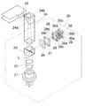
図1は第1の実施例の斜視図を示し、非接触距離センサ20においては、レーザーダイオード等の可干渉光源21、コリメータレンズ22、非偏光ビームスプリッタ23、光学式プローブ状偏光プリズム24が順次に配列され、プローブ状偏光プリズム24は偏光ビームスプリッタ面24aと基準ミラー面24bを有し、偏光面24aの反射方向のプローブ状偏光プリズム24の前面に、被測定部位であるスライダ側面25が配置されている。
【0017】
非偏光ビームスプリッタ23の反射方向には、開口板26、千鳥状位相回折格子等の4分割回折格子板27、1つの基板に厚さが異なる4つの領域28a〜28dを有する位相差水晶板28、45度方位に光学軸を有する45度方位偏光板29、4つの受光領域30a〜30dを有する4分割受光素子30が順次に配列されている。
【0018】
測定時には、可干渉光源21からの発散光Lは、コリメータレンズ22により略集光光とされ、非偏光ビームスプリッタ23を通って、プローブ状偏光プリズム24の偏光ビームスプリッタ面24aにおいて透過光と反射光に分割される。偏光面24aを反射したS偏波光は、スライダ側面25に向けてプローブ状偏光プリズム24を出射し、スライダ側面25で反射され、その反射光は元の光路を通ってプローブ状偏光プリズム24の偏光面24aまで戻される。一方、偏光面24aを透過したP偏波光は、プローブ状偏光プリズム24内部の基準ミラー面24bで反射され、同様に偏光面24aまで戻される。
【0019】
この両偏波光はプローブ状偏光プリズム24の偏光面24aにおいて合成され、後述する偏光干渉光学系によって干渉光束の明暗信号となる。プローブ状偏光プリズム24とスライダ側面25との距離が変化した場合には、偏光面24aで分離した2つの光束の往復の光路長差が可干渉光源21の波長の整数倍となる毎に、その明暗が変化する。即ち、可干渉光源21として波長0.78μmのレーザーダイオードを使用すれば、スライダ側面25との距離が0.39μmずれると、明暗が正弦波状に1周期分変化する。
【0020】
この明暗変化は受光素子30により電気信号に変換され、スライダ側面25との距離を予め明暗の中間となるような距離に設定しておけば、スライダ側面25との距離が微小に変化すると電気信号レベルが敏感に変化する。従って、この正弦波状の電気信号レベルの変化を利用して、波長0.39μmの1つの正弦波を数10の位相に分割可能な分解能の公知の電気回路を使用して、0.01μm程度の分解能で距離変化を検出することができる。また、2相の90度位相差明暗信号があれば、公知の電気的な内挿回路を使用して1つの正弦波を数10〜数100の位相に分割することができるので、更に高分解能な0.001μmの分解能で距離変化を検出することができる。
【0021】
図2は4相の90度位相差明暗信号の発生方法を示し、プローブ状偏光プリズム24から出射する段階では、2つの光束の波面は重ね合わさってはいるが、互いに直交する波面の直線偏光光束であり、干渉して明暗信号とはならない。これらの光束は、非偏光ビームスプリッタ23で反射され、開口板26の開口を通って、4分割回折格子板27によりそれぞれ直交した2つの直線偏光光束を含む4つの等価な光束に振幅分割される。このとき、これらの4つの光束は強度のみが分割により低下した状態で進行と共に分離してゆき、適切な空間に配置された水晶板28に入射する。
【0022】
この水晶板28は光学位相板として使用されており、f軸とs軸の2つの光学軸を有し、この間で屈折率に差があるために、光の電磁波における電界成分がf軸に平行に入射した直線偏波成分は、s軸に平行に入射した直線偏波成分に比べて位相が進んで射出される。このときの位相差Γ(deg)は、可干渉光源21の波長をλ、水晶の異常光線の屈折率をne、水晶の常光線の屈折率をno、水晶板28の厚さをtとして、次式で表される。
Γ=(360/λ)・(ne−no)t
【0023】
s軸に概略平行な直線偏波に対して異常光線屈折率neが対応し、f軸に平行な直線偏波光束に対して常光線屈折率noが対応する。水晶の屈折率の代表的な値はne=1.5477、no=1.5387なので、位相差Γ=90(deg)を満たすtを求めると、λ=0.78μm、ne=1.5477、no=1.5387を代入すると次のようになる。
t=λ/{4(ne―no)}=21.67μm
【0024】
本実施例においては、水晶板28は図3に示すように光学軸であるf軸がS偏波方向になるように配置され、田の字状の4つの異なる厚さになるようにエッチング処理によって段差が設けられており、4分割された光束はそれぞれの領域28a〜28dの中に入射して裏面から透過する。領域28aは段差加工されていない部分で水晶基板の元の厚さになっており、領域28bは領域28aに比較してS偏光成分のみ波面の位相が90度遅れるように、Δt=21.67μm相当を弗酸によりエッチング加工されている。
【0025】
領域28cは領域28aに比較してS偏光成分のみ波面の位相が180度遅れるように、2・Δt相当をエッチング加工されており、領域28dは領域28aに比較してS偏光成分のみ波面の位相が270度遅れるように3・Δt相当をエツチング加工されている。これらの3つの段差は、2・Δtの段差のエッチングを領域28c、28dにおいて1回行い、Δtの段差のエッチングを領域28a、28dにおいて1回行うことによって達成される。
【0026】
領域28aを透過した光束(P、S)は、水晶板28の元の厚さ及び光学軸の配置により、P、S偏波間でS偏波の波面の位相が相対的に進んでおり、この進み量をΔΦとする。領域28bを透過した光束(P、S)は、水晶板28の元の厚さよりエッチングによってΔtだけ薄くなっているので、S偏波の波面の位相の進みが90度だけ戻されて、位相の進み量はΔΦ−90度である。
【0027】
領域28cを透過した光束(P,S)は、水晶板28の元の厚さよりエッチングによって2・Δtだけ薄くなっているので、S偏波の波面の位相の進みが180度だけ戻されて、位相の進み量はΔΦ−180度である。領域28dを透過した光束(P,S)は、水晶板28の元の厚さよってエッチングによる3・Δtだけ薄くなっているので、S偏波の波面の位相の進みが270度だけ戻されて、位相の進み量はΔΦ−270度である。
【0028】
これら4つの領域28a〜28dを透過した光束(P,S)は、45度方位に光学軸を有する偏光板29により45度偏光成分が抽出されるが、このP、S偏波はそれぞれ位相情報を有したまま45度直線偏波に変換されるので、干渉を引き起こして明暗信号光束となる。このとき、それぞれの領域28a〜28dから射出した光束のP、S間の位相差は、λ/4の整数倍毎にずれているために、干渉光の明暗のタイミング(位相)は1/4周期毎にずれる。従って、これらそれぞれの干渉光束が4つの受光素子30a〜30dに入射することによって、同時に4つの位相差信号が得られる。この4つの干渉光束は1/4周期毎の位相ずれがあるために、90度位相差信号のA+相、B+相、A−相、B−相となり、これは4相プッシュプル信号である。
【0029】
本実施例では、4分割回折格子27、位相差水晶板28、45度方位偏光板29、4分割受光素子30a〜30dを整然と配置するだけなので、複数の微小な偏光板等を配置する作業等が不要となり、非常に簡単かつ小型な装置を実現することができる。特に、1つの大きな基板毎に回折格子27、水晶板28、偏光板29を半導体プロセスと同様の方法で加工し、最後に切断することによって容易に実現することができる。
【0030】
図4は第2の実施例のプッシュプル光学系の斜視図を示し、本実施例の水晶板31は、左右方向で2つの異なる厚さになるようにエッチング処理により段差が形成されて、光学軸であるf軸がS偏波方向になるように配置されている。この水晶板31は2つずつ4分割された光束がそれぞれ領域31a、31bに入射し、裏面から透過するようにされており、領域31aは段差加工されていない部分で、水晶基板の元の厚さになっている。また、領域31bは領域31aに比較して、S偏光成分のみがλ/4波面の位相が遅れるように段差加工されており、この段差はλ/2分の段差のエッチングを領域31bに1回行うことにより達成される。また、本実施例の偏光板32は、45度方位に光学軸を有する偏光板32aと135度方位に光学軸を有する偏光板32bが上下方向に配置されている。
【0031】
4分割回折格子板27において分割された光束(P,S)の内、左側の光束は水晶板31の領域31aを通り右側の光束は領域31bを通る。このとき、領域31aを透過した光束(P,S)は、水晶板31の元の厚さ及び光学軸の配置により、P、S偏波間でS偏波の波面の位相が相対的に進んでおり、この進み量をΔΦとする。領域31bを透過した光束(P,S)は、水晶板31の元の厚さよりエッチングによりΔtだけ薄くなっているので、S偏波の波面の位相の進みがλ/4だけ戻されて、位相の進み量はΔΦ−λ/4である。
【0032】
そして、これら2つの領域31a、31bを透過した光束(P,S)の内、上側の2光束は45度方位に偏光板32aを通り、下側の2光束は135度方位に偏光板32bを通って、それぞれ45度偏光成分又は135度偏光成分が抽出されるが、このときP、S偏波がそれぞれ位相情報を有したまま、45度又は135度の直線偏波に変換され、干渉を引き起こして明暗信号光束となる。
【0033】
2つの領域31a、31bから射出した光束P、S間の波面位相はλ/4ずれているので、偏光板32aの透過光束の干渉光束の明暗のタイミング(位相)は、領域31aの透過光束に比べて領域31bの透過光束が1/4周期進む。また、偏光板32bの透過光束の干渉光束の明暗のタイミング(位相)は、領域31a透過光束に比べて領域31bの透過光束が1/4周期進む。ここで、偏光板32aの透過光束の明暗位相と偏光板32bの透過光束の明暗位相は互いに180度位相がずれているので、4つの明暗光束の位相は0度、90度、180度、270度となり、第1の実施例と同様に4相プッシュプル信号となる。
【0034】
本実施例では、4分割回折格子27、位相差水晶板31、45度方位偏光板32a、135度方位偏光板32b、4分割受光素子30a〜30dを整然と配置するだけで、極めて簡単かつ小型に構成することができる。特に、水晶板31は1回のエッチング処理により加工することができ、偏光板32aと偏光板32bを隣り合わせに張り合わせることによって、比較的簡便に組立調整を行うことができる。
【0035】
なお、本実施例は2分割した可干渉光束を相対移動する回折格子に照明し、異なる次数の回折光を取り出して干渉位相信号を発生する格子干渉式エンコーダに適用することができる。また、他の一般的な格子干渉方式のエンコーダや干渉計測装置にも適用することも可能である。
【0036】
図5は第3の実施例の斜視図を示し、非接触センサ20においては、図1の場合と同様にレーザーダイオード等の可干渉光源21、コリメータレンズ22、非偏光ビームスプリッタ23、光学式プローブ状偏光プリズム24が順次に配置され、プローブ状偏光プリズム24は偏光ビームスプリッタ面24aと基準ミラー面24bを有し、偏光面24aの反射方向のプローブ状偏光プリズム24の前面に、非測定部位であるスライダ側面25が配置されている。
【0037】
非偏光ビームスプリッタ23の反射方向には、1/4波長板41、開口板42、千鳥状位相回折格子等の4分割回折格子板8、1つの基板状に4つの格子43a〜43dがその配列方位を45度ずつずらして形成されている偏光板マスク43、4つの領域44a〜44dを有する4分割受光素子44が順次に配列されている。
【0038】
測定時には、可干渉光源21からの発散光Lは、図1の場合と同様に、プローブ状偏光プリズム24の偏光ビームスプリッタ面24aにおいて透過光と反射光に分割される。偏光面24aを反射したS偏波光は、スライダ側面25に向けてプローブ状偏光プリズム24を射出し、スライダ側面25で反射され、プローブ状偏光プリズム24の偏光面24aまで戻される。一方、偏光面24aを透過したP偏波光は、同様に偏光面24aまで戻される。
【0039】
この両偏波光はプローブ状偏光プリズム24の偏光面24aにおいて合成され、後述する偏光干渉光学系によって干渉光束の明暗信号となる。プローブ状偏光プリズム24とスライダ側面25との距離が変化した場合には、偏光面24aで分離した2つの光束の往復の光路長差が可干渉光源21の波長の整数倍となる後とに、その明暗が変化する。
【0040】
この明暗変化は受光素子44により電気信号に変換され、図1の場合と同様に、高分解能で距離変化を検出することができる。
【0041】
図6は上述の4相の90度位相差明暗信号の発生方法を示し、プローブ状偏光プリズム24から射出する段階では、2つの光束の波面は重なり合ってはいるが、互いに直交する波面の直線偏光光束であり、干渉して明暗信号とはならない。これらは非偏光ビームスプリッタ23で反射され、1/4波長板41を透過して、それぞれが逆向きの円偏光に変換され、それらのベクトル合成された波面は1つの直線偏光となる。またその直線偏光の偏波面の向きは2光束間の位相差に依存し、2光束間で位相が360度ずれると、偏波面は180度回転する。
【0042】
この偏波面は回転する直線偏光光束は、開口板42の開口を通って、4分割回折格子板8により、それぞれ等価な直線偏光光束に振幅分割される。このときこれら4つの光束は強度のみが分割により低下した状態で信号と共に分離してゆき、適切な空間に配置された偏光板マスク43に入射する。
【0043】
この偏光板マスク43は光学的偏光板として機能するため、予めフォトリソグラフィプロセス等によって、ガラス板上に形成する際に自在にデザインすることが可能である。この実施例では、4相明暗信号を得るために90度ずつ明暗位相のずれた干渉信号を必要としているので、4つの光束が透過する領域ごとに、金属格子線の配列方位を45度ずつずらして形成してある。また、格子線のピッチは可干渉光源の波長より十分に小さくしている。
【0044】
回転する直線偏光は、格子線と直交する場合と、一致する場合で、透過光が最大、最小になるので、4つの領域ごとに明暗のタイミングが異なる位相差信号が得られる。
【0045】
本実施例では、1/4波長板41、開口板42、偏光板マスク43、4分割受光素子44を整然と配置するだけなので極めて簡単かつ小型に構成することができ位相差が高精度に確定する。
【0046】
なお、本実施例は2分割した可干渉光束を相対移動する回折格子に照明し、異なる次数の回折光を取り出して干渉信号を発生する格子干渉式エンコーダに適用することができる。また、他の一般的な格子干渉方式のエンコーダや干渉計測装置にも適用することができる。
【0047】
【発明の効果】
以上説明したように本発明に係る干渉式計測装置及び格子干渉式エンコーダは、光学系を極めて簡素にかつ小型に実現することができ、かつ複数の安定した位相差信号を一括して検出して、高精度の計測を行うことができる。
【0048】
また、本発明に係る光学装置はこのような計測装置を実現可能とする。
【図面の簡単な説明】
【図1】第1の実施例の干渉計測装置の斜視図である。
【図2】位相差水晶板による波面の位相ずれの説明図である。
【図3】プッシュプル光学系の斜視図である。
【図4】第2の実施例のプッシュプル光学系の斜視図である。
【図5】第3の実施例の干渉計測装置の斜視図である。
【図6】格子ユニットによる透過偏光光束装置の説明図である。
【図7】従来例の干渉計測装置の斜視図である。
【符号の説明】
21 可干渉光源
22 コリメータレンズ
23 非偏光ビームスプリッタ
24 プローブ状偏光プリズム
25 スライダ側面
26、42 開口板
27 回折格子板
28、31 水晶板
29、32 偏光板
30、44 受光素子
41 1/4波長板
43 偏光板マスク [0001]
BACKGROUND OF THE INVENTION
The present invention relates to an interference measuring apparatus and a grating interference encoder that generate a phase difference signal and measure a length and an angle with high accuracy in industrial equipment such as FA (Factory Automation).
[0002]
[Prior art]
Conventionally, laser interferometers and incremental encoders have been used as high-precision positioning devices such as FA. These devices detect the relative position shift by converting the position shift into a pulse train and counting the number of pulses at this time. At this time, since it is necessary to detect the moving direction, normally, two or more phase difference signals A phase and B phase are output, and a one-cycle sine wave signal is set to 360 degrees to give a phase shift of 90 degrees. It is done.
[0003]
In such a high-resolution incremental encoder or laser interferometer, two detection optical systems are arranged with their spatial positions shifted to generate a phase difference signal of A phase and B phase, or orthogonal to each other. The polarized light beams interfere with each other through a half-wave plate, and are converted into one linearly polarized light beam whose polarization direction rotates in accordance with the phase difference of the wavefront between the two light beams, and then further divided into a plurality of light beams, There has been known a method of generating a phase difference signal light beam by transmitting through a polarizing plate arranged with a polarization axis shifted in different directions.
[0004]
FIG. 7 is a perspective view of a conventional laser interference type non-contact distance sensor. The laser light L from the
[0005]
On the other hand, the P-polarized light transmitted through the
[0006]
[Problems to be solved by the invention]
However, in the above-described conventional example, since the phase shift is given by the arrangement of the polarizing
[0007]
An object of the present invention is to provide a small and easy to assemble interference measuring apparatus that collectively detects a plurality of stable phase difference signals in view of the above-described conventional example.
[0008]
Another object of the present invention is to provide a measuring apparatus such as a small and highly accurate grating interference encoder.
[0009]
[Means for Solving the Problems]
In order to achieve the above object, an interference measuring apparatus according to the present invention divides a coherent beam into two parts, modulates the phase of the wave front of the beam passing through each optical path, and forms linearly polarized beams orthogonal to each other. An optical member for superimposing the wavefronts of the light flux again, a light splitting member for dividing the light flux superimposed by the optical member into a plurality of light fluxes, and a plurality of regions having different thicknesses according to the incident positions of the plurality of light fluxes A crystal plate formed on a single substrate, a polarizing plate for extracting each light beam transmitted through the crystal plate with a 45-degree polarization component with respect to the optical axis of the crystal plate, and receiving each light beam transmitted through the polarizing plate And a plurality of light receiving means for generating different interference phase signals.
[0010]
Further, the interference measuring apparatus according to the present invention divides the coherent light beam into two parts, modulates the phase of the wave front of the light beam passing through the respective optical paths to form linearly polarized light beams orthogonal to each other, and reshapes the wave front of the linearly polarized light beam again. An optical member for superimposing, a light dividing member for dividing the light beam superimposed by the optical member into four light beams, and two regions having different thicknesses according to the incident positions of the four light beams are formed on one substrate a crystal plate formed in, among the four light beams transmitted through the quartz plate, the removed two regions two light flux transmitted through respectively 45 ° polarization component with respect to the optical axis of said quartz plate, said four A polarizing plate for extracting the other two light beams of the light beam with a 135-degree polarization component; and a light receiving means for receiving each light beam transmitted through the polarizing plate and generating a plurality of different interference phase signals. To do.
[0012]
A grating interference encoder according to the present invention includes an optical member for superimposing wavefronts of diffracted lights of different orders generated by a diffraction grating relatively moving from a coherent beam as linearly polarized beams orthogonal to each other, and the optical member A light splitting member for splitting a light beam superposed by a member into a plurality of light beams, a crystal plate in which a plurality of regions having different thicknesses are formed on a single substrate in accordance with an incident position of the plurality of light beams, and the crystal plate a polarizing plate that each light beam is taken out at 45 degree polarization component with respect to the optical axis of said quartz plate which has passed through a light receiving means for receiving a respective light beam transmitted through the polarizing plate to generate a plurality of different interference phase signal It is characterized by having.
[0013]
A grating interference encoder according to the present invention includes an optical member for superimposing wavefronts of diffracted lights having different orders generated by a diffraction grating relatively moving from a coherent light beam as linearly polarized light beams orthogonal to each other, and the optical member A light splitting member for splitting a light beam superposed by the member into four light beams, a crystal plate in which two regions having different thicknesses are formed on a single substrate in accordance with an incident position of the four light beams, and the crystal plate Of the four luminous fluxes transmitted through the two regions, the two luminous fluxes respectively transmitted through the two regions are extracted with a 45-degree polarization component with respect to the optical axis of the quartz plate, and the other two luminous fluxes out of the four luminous fluxes are 135. And a light receiving unit that receives each light beam transmitted through the polarizing plate and generates a plurality of different interference phase signals.
[0016]
DETAILED DESCRIPTION OF THE INVENTION
The present invention will be described in detail based on the embodiment shown in FIGS.
FIG. 1 shows a perspective view of the first embodiment. In the
[0017]
In the reflection direction of the
[0018]
At the time of measurement, the divergent light L from the
[0019]
The two polarized lights are combined on the
[0020]
This light / dark change is converted into an electric signal by the
[0021]
FIG. 2 shows a method for generating a four-phase 90-degree phase difference light / dark signal. At the stage of emission from the probe-like
[0022]
This
Γ = (360 / λ) · (ne−no) t
[0023]
The extraordinary ray refractive index ne corresponds to a linearly polarized wave substantially parallel to the s axis, and the ordinary ray refractive index no corresponds to a linearly polarized light beam parallel to the f axis. Since the typical values of the refractive index of quartz are ne = 1.5477 and no = 1.5387, when t satisfying the phase difference Γ = 90 (deg) is obtained, λ = 0.78 μm, ne = 1.5477, Substituting no = 1.5387 results in the following.
t = λ / {4 (ne-no)} = 21.67 μm
[0024]
In this embodiment, the
[0025]
The
[0026]
The light beam (P, S) transmitted through the
[0027]
Since the light flux (P, S) transmitted through the
[0028]
The luminous flux (P, S) transmitted through these four
[0029]
In this embodiment, the four-divided
[0030]
FIG. 4 is a perspective view of the push-pull optical system of the second embodiment. The
[0031]
Of the light beams (P, S) divided by the four-divided
[0032]
Of the light beams (P, S) transmitted through these two
[0033]
Since the wavefront phase between the light beams P and S emitted from the two
[0034]
In this embodiment, the four-divided
[0035]
The present embodiment can be applied to a grating interference encoder that illuminates a diffraction grating that relatively moves a coherent light beam divided into two parts, extracts diffracted lights of different orders, and generates an interference phase signal. Further, the present invention can also be applied to other general grating interference type encoders and interference measuring apparatuses.
[0036]
FIG. 5 shows a perspective view of the third embodiment. In the
[0037]
The reflection direction of the
[0038]
At the time of measurement, the diverging light L from the coherent
[0039]
The two polarized lights are combined on the
[0040]
This light / dark change is converted into an electric signal by the
[0041]
FIG. 6 shows a method for generating the above-described four-phase 90-degree phase difference light / dark signal. At the stage of emission from the probe-like
[0042]
The linearly polarized light beam rotating on the polarization plane passes through the opening of the
[0043]
Since this
[0044]
The rotated linearly polarized light has the maximum and minimum transmitted light when orthogonal to the lattice line and when it coincides, so that a phase difference signal with different brightness timing is obtained for each of the four regions.
[0045]
In this embodiment, the
[0046]
Note that this embodiment can be applied to a grating interference encoder that illuminates a diffraction grating that relatively moves a coherent light beam divided into two parts, extracts diffracted lights of different orders, and generates an interference signal. Further, the present invention can be applied to other general grating interference type encoders and interference measuring apparatuses.
[0047]
【The invention's effect】
As described above, the interferometric measuring apparatus and the grating interferometric encoder according to the present invention can realize an optical system extremely simply and compactly, and collectively detect a plurality of stable phase difference signals. Highly accurate measurement can be performed.
[0048]
The optical device according to the present invention can realize such a measuring device.
[Brief description of the drawings]
FIG. 1 is a perspective view of an interference measuring apparatus according to a first embodiment.
FIG. 2 is an explanatory diagram of a wavefront phase shift caused by a phase difference crystal plate.
FIG. 3 is a perspective view of a push-pull optical system.
FIG. 4 is a perspective view of a push-pull optical system according to a second embodiment.
FIG. 5 is a perspective view of an interference measuring apparatus according to a third embodiment.
FIG. 6 is an explanatory diagram of a transmitted polarized light beam device using a grating unit.
FIG. 7 is a perspective view of a conventional interference measurement apparatus.
[Explanation of symbols]
21
27
43 polarizing plate mask
Claims (6)
該光学部材により重ね合わせた光束を複数の光束に分割する光分割部材と、
前記複数の光束の入射位置に応じて互いに厚みの異なる複数の領域を1枚の基板に形成した水晶板と、
該水晶板を透過した各光束を該水晶板の光軸に対して45度偏光成分で取り出す偏光板と、
該偏光板を透過した各光束を受光して複数の互いに異なる干渉位相信号を発生する受光手段とを有することを特徴とする干渉計測装置。An optical member for dividing the coherent light beam into two, modulating the phase of the wavefront of the light beam passing through the respective optical paths into a linearly polarized light beam orthogonal to each other, and superimposing the wavefronts of the linearly polarized light beam again;
A light splitting member for splitting the light beam superimposed by the optical member into a plurality of light beams;
A crystal plate in which a plurality of regions having different thicknesses are formed on a single substrate according to the incident positions of the plurality of light beams;
A polarizing plate for extracting each light beam transmitted through the quartz plate with a 45-degree polarization component with respect to the optical axis of the quartz plate;
An interference measuring apparatus comprising: a light receiving unit that receives each light beam transmitted through the polarizing plate and generates a plurality of different interference phase signals.
該光学部材により重ね合わせた光束を4つの光束に分割する光分割部材と、
前記4つの光束の入射位置に応じて互いに厚みの異なる2つの領域を1枚の基板に形成した水晶板と、
該水晶板を透過した4つの光束のうち、前記2つの領域をそれぞれ透過した2つの光束を該水晶板の光軸に対して45度偏光成分で取り出し、前記4つの光束のうち他の2つの光束を135度偏光成分で取り出す偏光板と、
該偏光板を透過した各光束を受光して複数の互いに異なる干渉位相信号を発生する受光手段とを有することを特徴とする干渉計測装置。An optical member for dividing the coherent light beam into two, modulating the phase of the wavefront of the light beam passing through the respective optical paths into a linearly polarized light beam orthogonal to each other, and superimposing the wavefronts of the linearly polarized light beam again;
A light splitting member for splitting the light flux superimposed by the optical member into four light fluxes;
A quartz plate in which two regions having different thicknesses are formed on a single substrate according to the incident positions of the four light beams;
Of the four luminous fluxes transmitted through the quartz plate, two luminous fluxes respectively transmitted through the two regions are extracted with a 45-degree polarization component with respect to the optical axis of the quartz plate, and the other two of the four luminous fluxes A polarizing plate for extracting a light beam with a 135-degree polarization component;
An interference measuring apparatus comprising: a light receiving unit that receives each light beam transmitted through the polarizing plate and generates a plurality of different interference phase signals.
該光学部材により重ね合わせた光束を複数の光束に分割する光分割部材と、
前記複数の光束の入射位置に応じて互いに厚みの異なる複数の領域を1枚の基板に形成した水晶板と、
該水晶板を透過した各光束を該水晶板の光軸に対して45度偏光成分で取り出す偏光板と、
該偏光板を透過した各光束を受光して複数の互いに異なる干渉位相信号を発生する受光手段とを有することを特徴とする格子干渉式エンコーダ。An optical member for superimposing wavefronts of mutually different orders of diffracted light generated by a diffraction grating relatively moving from a coherent light beam as linearly polarized light beams orthogonal to each other;
A light splitting member for splitting the light beam superimposed by the optical member into a plurality of light beams;
A crystal plate in which a plurality of regions having different thicknesses are formed on a single substrate according to the incident positions of the plurality of light beams;
A polarizing plate for extracting each light beam transmitted through the quartz plate with a 45-degree polarization component with respect to the optical axis of the quartz plate;
A grating interference encoder comprising: a light receiving unit that receives each light beam transmitted through the polarizing plate and generates a plurality of different interference phase signals.
該光学部材により重ね合わせた光束を4つの光束に分割する光分割部材と、
前記4つの光束の入射位置に応じて互いに厚みの異なる2つの領域を1枚の基板に形成した水晶板と、
該水晶板を透過した4つの光束のうち、前記2つの領域をそれぞれ透過した2つの光束を該水晶板の光軸に対して45度偏光成分で取り出し、前記4つの光束のうち他の2つの光束を135度偏光成分で取り出す偏光板と、
該偏光板を透過した各光束を受光して複数の互いに異なる干渉位相信号を発生する受光手段とを有することを特徴とする格子干渉式エンコーダ。An optical member for superimposing wavefronts of diffracted light beams of different orders generated by a diffraction grating relatively moving from a coherent light beam as linearly polarized light beams orthogonal to each other;
A light splitting member for splitting the light flux superimposed by the optical member into four light fluxes;
A quartz plate in which two regions having different thicknesses are formed on a single substrate according to the incident positions of the four light beams;
Of the four luminous fluxes transmitted through the quartz plate, two luminous fluxes respectively transmitted through the two regions are extracted with a 45-degree polarization component with respect to the optical axis of the quartz plate, and the other two of the four luminous fluxes A polarizing plate for extracting a light beam with a 135-degree polarization component;
A grating interference encoder comprising: a light receiving unit that receives each light beam transmitted through the polarizing plate and generates a plurality of different interference phase signals.
Priority Applications (5)
| Application Number | Priority Date | Filing Date | Title |
|---|---|---|---|
| JP06679899A JP4365927B2 (en) | 1999-03-12 | 1999-03-12 | Interference measuring device and grating interference encoder |
| US09/523,312 US6657181B1 (en) | 1999-03-12 | 2000-03-10 | Optical element used in compact interference measuring apparatus detecting plurality of phase difference signals |
| EP00105083A EP1037019A3 (en) | 1999-03-12 | 2000-03-10 | Interference measuring apparatus |
| US10/425,680 US7034947B2 (en) | 1999-03-12 | 2003-04-30 | Compact interference measuring apparatus for detecting the magnitude and direction of positional deviation |
| US11/335,565 US7375820B2 (en) | 1999-03-12 | 2006-01-20 | Interference measuring apparatus for detecting a plurality of stable phase difference signals |
Applications Claiming Priority (1)
| Application Number | Priority Date | Filing Date | Title |
|---|---|---|---|
| JP06679899A JP4365927B2 (en) | 1999-03-12 | 1999-03-12 | Interference measuring device and grating interference encoder |
Publications (3)
| Publication Number | Publication Date |
|---|---|
| JP2000258124A JP2000258124A (en) | 2000-09-22 |
| JP2000258124A5 JP2000258124A5 (en) | 2006-04-27 |
| JP4365927B2 true JP4365927B2 (en) | 2009-11-18 |
Family
ID=13326261
Family Applications (1)
| Application Number | Title | Priority Date | Filing Date |
|---|---|---|---|
| JP06679899A Expired - Fee Related JP4365927B2 (en) | 1999-03-12 | 1999-03-12 | Interference measuring device and grating interference encoder |
Country Status (3)
| Country | Link |
|---|---|
| US (3) | US6657181B1 (en) |
| EP (1) | EP1037019A3 (en) |
| JP (1) | JP4365927B2 (en) |
Families Citing this family (17)
| Publication number | Priority date | Publication date | Assignee | Title |
|---|---|---|---|---|
| JP4846909B2 (en) * | 2000-02-15 | 2011-12-28 | キヤノン株式会社 | Optical encoder and diffraction grating displacement measuring method |
| JP2004212243A (en) * | 2003-01-06 | 2004-07-29 | Canon Inc | Grating interference type optical encoder |
| US7230717B2 (en) * | 2003-08-28 | 2007-06-12 | 4D Technology Corporation | Pixelated phase-mask interferometer |
| JP2006163291A (en) * | 2004-12-10 | 2006-06-22 | Canon Inc | Optical element and manufacturing method thereof |
| US7466426B2 (en) * | 2005-12-14 | 2008-12-16 | General Electric Company | Phase shifting imaging module and method of imaging |
| JP4852318B2 (en) * | 2006-02-20 | 2012-01-11 | 株式会社マグネスケール | Displacement detector, polarizing beam splitter, and diffraction grating |
| EP2013570A1 (en) * | 2006-04-28 | 2009-01-14 | Micronic Laser Systems Ab | Method and apparatus for recording of images and study of surfaces |
| JP2008286518A (en) | 2007-05-15 | 2008-11-27 | Hitachi Ltd | Method and device for measuring displacement thereof |
| JP5523664B2 (en) * | 2007-11-06 | 2014-06-18 | 株式会社ミツトヨ | Interferometer |
| JP5381371B2 (en) * | 2008-11-07 | 2014-01-08 | 株式会社リコー | Polarization separation device, optical scanning device, and image forming apparatus |
| JP5395603B2 (en) | 2009-10-05 | 2014-01-22 | 太陽誘電株式会社 | Regenerative brake device and electric assist vehicle equipped with the same |
| EP2487453B1 (en) * | 2009-10-05 | 2016-12-14 | Taiyo Yuden Co., Ltd. | Displacement measurement method and displacement measurement device |
| TWI417519B (en) * | 2009-12-10 | 2013-12-01 | Ind Tech Res Inst | Interference phase difference measurement method and system |
| JP5699105B2 (en) * | 2012-04-11 | 2015-04-08 | 株式会社日立製作所 | Surface measurement method and apparatus |
| EP2792996A1 (en) * | 2013-04-17 | 2014-10-22 | Nederlandse Organisatie voor toegepast -natuurwetenschappelijk onderzoek TNO | Interferometric distance sensing device and method |
| CN109238148B (en) | 2018-09-13 | 2020-10-27 | 清华大学 | Five-degree-of-freedom heterodyne grating interferometry system |
| CN112630879B (en) * | 2020-12-25 | 2022-09-30 | 中国工程物理研究院激光聚变研究中心 | Phase delay element and phase delay device |
Family Cites Families (46)
| Publication number | Priority date | Publication date | Assignee | Title |
|---|---|---|---|---|
| US3316799A (en) * | 1962-11-07 | 1967-05-02 | Barnes Eng Co | Two axis autocollimator using polarized light |
| DE2127483A1 (en) | 1971-06-03 | 1972-12-14 | Leitz Ernst Gmbh | Procedure for the interferential measurement of lengths, angles, differences in gait or speeds |
| FR2615281B1 (en) * | 1987-05-11 | 1996-08-23 | Canon Kk | DEVICE FOR MEASURING A RELATIVE MOTION DISTANCE OF TWO MOBILE OBJECTS IN RELATION TO ONE ANOTHER |
| US5172186A (en) * | 1990-07-03 | 1992-12-15 | Konica Corporation | Laser interferometry length measuring an apparatus employing a beam slitter |
| DE4033013C2 (en) * | 1990-10-18 | 1994-11-17 | Heidenhain Gmbh Dr Johannes | Polarization-optical arrangement |
| JP3066923B2 (en) | 1991-07-29 | 2000-07-17 | キヤノン株式会社 | Encoder and system having the same |
| US5283434A (en) | 1991-12-20 | 1994-02-01 | Canon Kabushiki Kaisha | Displacement detecting device with integral optics |
| GB9127191D0 (en) * | 1991-12-21 | 1992-02-19 | T & N Technology Ltd | Flanged bearings |
| WO1993016469A1 (en) | 1992-02-07 | 1993-08-19 | Sony Corporation | Phase varying device, and optical pickup apparatus using the same for magneto-optical storage |
| EP0561015A1 (en) * | 1992-03-17 | 1993-09-22 | International Business Machines Corporation | Interferometric phase-measuring |
| US5390022A (en) | 1992-04-07 | 1995-02-14 | Canon Kabushiki Kaisha | Displacement information detection apparatus for receiving a divergent light beam |
| JP2899165B2 (en) | 1992-05-15 | 1999-06-02 | キヤノン株式会社 | Doppler speedometer and displacement information detector |
| JP3254737B2 (en) | 1992-06-17 | 2002-02-12 | キヤノン株式会社 | encoder |
| JP3478567B2 (en) | 1992-09-25 | 2003-12-15 | キヤノン株式会社 | Rotation information detection device |
| JPH06194123A (en) | 1992-12-24 | 1994-07-15 | Canon Inc | Displacement detecting device |
| JP3210111B2 (en) | 1992-12-24 | 2001-09-17 | キヤノン株式会社 | Displacement detector |
| JP3173208B2 (en) | 1993-01-29 | 2001-06-04 | キヤノン株式会社 | Displacement measuring device |
| JP3083019B2 (en) | 1993-03-05 | 2000-09-04 | キヤノン株式会社 | Optical device and speed information detecting device |
| US5424535A (en) * | 1993-04-29 | 1995-06-13 | The Boeing Company | Optical angle sensor using polarization techniques |
| JP3082516B2 (en) | 1993-05-31 | 2000-08-28 | キヤノン株式会社 | Optical displacement sensor and drive system using the optical displacement sensor |
| US5502466A (en) | 1993-06-29 | 1996-03-26 | Canon Kabushiki Kaisha | Doppler velocimeter and position information detection apparatus for use with objects having variations in surface depth |
| JP3028716B2 (en) | 1993-09-29 | 2000-04-04 | キヤノン株式会社 | Optical displacement sensor |
| JP3530573B2 (en) | 1994-04-27 | 2004-05-24 | キヤノン株式会社 | Optical displacement sensor |
| CA2122782C (en) * | 1994-05-03 | 1999-07-27 | Wojtek J. Bock | Apparatus for measuring an ambient physical parameter applied to a highly birefringent sensing fiber and method |
| JP3495783B2 (en) * | 1994-05-13 | 2004-02-09 | キヤノン株式会社 | Encoder |
| JP3491969B2 (en) | 1994-06-27 | 2004-02-03 | キヤノン株式会社 | Displacement information measuring device |
| JP3513247B2 (en) | 1994-07-11 | 2004-03-31 | キヤノン株式会社 | Frequency shifter and optical displacement measuring device using the same |
| JP3450446B2 (en) | 1994-08-03 | 2003-09-22 | キヤノン株式会社 | Optical displacement detector |
| US5815267A (en) | 1994-09-09 | 1998-09-29 | Canon Kabushiki Kaisha | Displacement information measuring apparatus in which a light-receiving condition on a photodetector is adjustable |
| JPH08210814A (en) | 1994-10-12 | 1996-08-20 | Canon Inc | Optical displacement measuring instrument |
| JPH08219812A (en) | 1995-02-15 | 1996-08-30 | Canon Inc | Device and scale for detecting displacement information, and drive control device using it |
| DE69622297T2 (en) | 1995-02-21 | 2002-11-21 | Canon Kk | Device for determining a displacement and its use in a drive control device |
| US5796470A (en) | 1995-02-28 | 1998-08-18 | Canon Kabushiki Kaisha | Frequency shifter and optical displacement measuring apparatus using the frequency shifter |
| JP3492012B2 (en) | 1995-03-09 | 2004-02-03 | キヤノン株式会社 | Displacement information detection device |
| JPH08304430A (en) | 1995-05-12 | 1996-11-22 | Canon Inc | Frequency shifter and optical displacement measuring apparatus using it |
| JP3548275B2 (en) | 1995-05-12 | 2004-07-28 | キヤノン株式会社 | Displacement information measuring device |
| US5932116A (en) * | 1995-06-05 | 1999-08-03 | Tohoku Unicom Co., Ltd. | Power supply for multi-electrode discharge |
| US6229140B1 (en) | 1995-10-27 | 2001-05-08 | Canon Kabushiki Kaisha | Displacement information detection apparatus |
| JP3647135B2 (en) | 1996-04-15 | 2005-05-11 | キヤノン株式会社 | Optical displacement information measuring device |
| US6151185A (en) | 1996-09-05 | 2000-11-21 | Canon Kabushiki Kaisha | Position detecting apparatus, positioning apparatus, and information recording apparatus using the same |
| DE19652113A1 (en) * | 1996-12-14 | 1998-06-18 | Johannes Prof Dr Schwider | Automated phase division evaluation method for interferometer, used, e.g., in CCD array |
| US6075235A (en) * | 1997-01-02 | 2000-06-13 | Chun; Cornell Seu Lun | High-resolution polarization-sensitive imaging sensors |
| US6631047B2 (en) | 1997-09-22 | 2003-10-07 | Canon Kabushiki Kaisha | Interference device, position detecting device, positioning device and information recording apparatus using the same |
| JPH11351813A (en) | 1998-06-08 | 1999-12-24 | Canon Inc | Interference apparatus and position detector using the same |
| EP1045227B2 (en) * | 1999-04-16 | 2012-04-18 | Canon Kabushiki Kaisha | Encoder |
| US6304330B1 (en) * | 1999-10-06 | 2001-10-16 | Metrolaser, Inc. | Methods and apparatus for splitting, imaging, and measuring wavefronts in interferometry |
-
1999
- 1999-03-12 JP JP06679899A patent/JP4365927B2/en not_active Expired - Fee Related
-
2000
- 2000-03-10 US US09/523,312 patent/US6657181B1/en not_active Expired - Fee Related
- 2000-03-10 EP EP00105083A patent/EP1037019A3/en not_active Withdrawn
-
2003
- 2003-04-30 US US10/425,680 patent/US7034947B2/en not_active Expired - Fee Related
-
2006
- 2006-01-20 US US11/335,565 patent/US7375820B2/en not_active Expired - Fee Related
Also Published As
| Publication number | Publication date |
|---|---|
| JP2000258124A (en) | 2000-09-22 |
| EP1037019A3 (en) | 2001-11-07 |
| US7375820B2 (en) | 2008-05-20 |
| US7034947B2 (en) | 2006-04-25 |
| US6657181B1 (en) | 2003-12-02 |
| US20060114474A1 (en) | 2006-06-01 |
| EP1037019A2 (en) | 2000-09-20 |
| US20030223075A1 (en) | 2003-12-04 |
Similar Documents
| Publication | Publication Date | Title |
|---|---|---|
| US7375820B2 (en) | Interference measuring apparatus for detecting a plurality of stable phase difference signals | |
| JP2603305B2 (en) | Displacement measuring device | |
| KR101876816B1 (en) | Displacement detecting device | |
| JPH07101181B2 (en) | Position detector and position measuring method | |
| US5321502A (en) | Measuring method and measuring apparatus | |
| JP2004144581A (en) | Displacement detecting apparatus | |
| JP2683117B2 (en) | encoder | |
| JPS63277926A (en) | Length measuring instrument | |
| JPH0794969B2 (en) | Positioning method and device thereof | |
| JP2001336952A (en) | Measuring apparatus | |
| JPH046884B2 (en) | ||
| JP3185373B2 (en) | Encoder | |
| JP4404184B2 (en) | Displacement detector | |
| JP3038860B2 (en) | Encoder | |
| JPS59163517A (en) | Optical scale reader | |
| JPH02298804A (en) | Interferometer | |
| JPH05126603A (en) | Grating interference measuring device | |
| JP2675317B2 (en) | Moving amount measuring method and moving amount measuring device | |
| JP2931082B2 (en) | Method and apparatus for measuring small displacement | |
| JP2003035570A (en) | Diffraction interference type linear scale | |
| JP3118992B2 (en) | measuring device | |
| JP2683098B2 (en) | encoder | |
| JP2600888B2 (en) | Encoder | |
| JPH0454405A (en) | Optical displacement gauge | |
| JPH05107042A (en) | Method and apparatus for detecting position using diffraction grating |
Legal Events
| Date | Code | Title | Description |
|---|---|---|---|
| A521 | Request for written amendment filed |
Free format text: JAPANESE INTERMEDIATE CODE: A523 Effective date: 20060308 |
|
| A621 | Written request for application examination |
Free format text: JAPANESE INTERMEDIATE CODE: A621 Effective date: 20060308 |
|
| A977 | Report on retrieval |
Free format text: JAPANESE INTERMEDIATE CODE: A971007 Effective date: 20080402 |
|
| A131 | Notification of reasons for refusal |
Free format text: JAPANESE INTERMEDIATE CODE: A131 Effective date: 20080701 |
|
| A521 | Request for written amendment filed |
Free format text: JAPANESE INTERMEDIATE CODE: A523 Effective date: 20080901 |
|
| A131 | Notification of reasons for refusal |
Free format text: JAPANESE INTERMEDIATE CODE: A131 Effective date: 20081209 |
|
| A521 | Request for written amendment filed |
Free format text: JAPANESE INTERMEDIATE CODE: A523 Effective date: 20090206 |
|
| A131 | Notification of reasons for refusal |
Free format text: JAPANESE INTERMEDIATE CODE: A131 Effective date: 20090526 |
|
| A521 | Request for written amendment filed |
Free format text: JAPANESE INTERMEDIATE CODE: A523 Effective date: 20090727 |
|
| TRDD | Decision of grant or rejection written | ||
| A01 | Written decision to grant a patent or to grant a registration (utility model) |
Free format text: JAPANESE INTERMEDIATE CODE: A01 Effective date: 20090818 |
|
| A01 | Written decision to grant a patent or to grant a registration (utility model) |
Free format text: JAPANESE INTERMEDIATE CODE: A01 |
|
| A61 | First payment of annual fees (during grant procedure) |
Free format text: JAPANESE INTERMEDIATE CODE: A61 Effective date: 20090824 |
|
| FPAY | Renewal fee payment (event date is renewal date of database) |
Free format text: PAYMENT UNTIL: 20120828 Year of fee payment: 3 |
|
| R150 | Certificate of patent or registration of utility model |
Free format text: JAPANESE INTERMEDIATE CODE: R150 |
|
| FPAY | Renewal fee payment (event date is renewal date of database) |
Free format text: PAYMENT UNTIL: 20120828 Year of fee payment: 3 |
|
| FPAY | Renewal fee payment (event date is renewal date of database) |
Free format text: PAYMENT UNTIL: 20130828 Year of fee payment: 4 |
|
| LAPS | Cancellation because of no payment of annual fees |