JP4342111B2 - Current pulse receiver circuit - Google Patents
Current pulse receiver circuit Download PDFInfo
- Publication number
- JP4342111B2 JP4342111B2 JP2001021224A JP2001021224A JP4342111B2 JP 4342111 B2 JP4342111 B2 JP 4342111B2 JP 2001021224 A JP2001021224 A JP 2001021224A JP 2001021224 A JP2001021224 A JP 2001021224A JP 4342111 B2 JP4342111 B2 JP 4342111B2
- Authority
- JP
- Japan
- Prior art keywords
- circuit
- voltage
- current
- output
- input
- Prior art date
- Legal status (The legal status is an assumption and is not a legal conclusion. Google has not performed a legal analysis and makes no representation as to the accuracy of the status listed.)
- Expired - Fee Related
Links
- 238000006243 chemical reaction Methods 0.000 claims description 129
- 239000000872 buffer Substances 0.000 claims description 100
- 230000000694 effects Effects 0.000 claims description 39
- 230000008878 coupling Effects 0.000 claims description 34
- 238000010168 coupling process Methods 0.000 claims description 34
- 238000005859 coupling reaction Methods 0.000 claims description 34
- 238000001514 detection method Methods 0.000 claims description 30
- 230000007423 decrease Effects 0.000 claims description 23
- 230000003321 amplification Effects 0.000 claims description 15
- 238000003199 nucleic acid amplification method Methods 0.000 claims description 15
- 230000010354 integration Effects 0.000 claims description 11
- 230000000295 complement effect Effects 0.000 claims description 7
- 230000003287 optical effect Effects 0.000 description 41
- 238000010586 diagram Methods 0.000 description 39
- 238000004891 communication Methods 0.000 description 31
- 230000004044 response Effects 0.000 description 20
- 230000007704 transition Effects 0.000 description 17
- 230000008859 change Effects 0.000 description 12
- 230000004069 differentiation Effects 0.000 description 9
- 239000003990 capacitor Substances 0.000 description 8
- 238000007796 conventional method Methods 0.000 description 6
- 102100022511 Cadherin-like protein 26 Human genes 0.000 description 5
- 101000899450 Homo sapiens Cadherin-like protein 26 Proteins 0.000 description 5
- 230000003247 decreasing effect Effects 0.000 description 5
- 230000006872 improvement Effects 0.000 description 5
- 230000007257 malfunction Effects 0.000 description 5
- 230000009467 reduction Effects 0.000 description 4
- 230000004048 modification Effects 0.000 description 3
- 238000012986 modification Methods 0.000 description 3
- 230000005540 biological transmission Effects 0.000 description 2
- 238000007599 discharging Methods 0.000 description 2
- 239000002356 single layer Substances 0.000 description 2
- 230000001133 acceleration Effects 0.000 description 1
- 230000009471 action Effects 0.000 description 1
- 230000001934 delay Effects 0.000 description 1
- 230000006866 deterioration Effects 0.000 description 1
- 230000002542 deteriorative effect Effects 0.000 description 1
- 238000005516 engineering process Methods 0.000 description 1
- 238000005286 illumination Methods 0.000 description 1
- 238000000034 method Methods 0.000 description 1
- 239000013307 optical fiber Substances 0.000 description 1
- 230000000644 propagated effect Effects 0.000 description 1
Images


Classifications
-
- H—ELECTRICITY
- H04—ELECTRIC COMMUNICATION TECHNIQUE
- H04B—TRANSMISSION
- H04B10/00—Transmission systems employing electromagnetic waves other than radio-waves, e.g. infrared, visible or ultraviolet light, or employing corpuscular radiation, e.g. quantum communication
- H04B10/60—Receivers
- H04B10/66—Non-coherent receivers, e.g. using direct detection
- H04B10/69—Electrical arrangements in the receiver
- H04B10/693—Arrangements for optimizing the preamplifier in the receiver
- H04B10/6933—Offset control of the differential preamplifier
-
- H—ELECTRICITY
- H03—ELECTRONIC CIRCUITRY
- H03F—AMPLIFIERS
- H03F3/00—Amplifiers with only discharge tubes or only semiconductor devices as amplifying elements
- H03F3/04—Amplifiers with only discharge tubes or only semiconductor devices as amplifying elements with semiconductor devices only
- H03F3/08—Amplifiers with only discharge tubes or only semiconductor devices as amplifying elements with semiconductor devices only controlled by light
- H03F3/087—Amplifiers with only discharge tubes or only semiconductor devices as amplifying elements with semiconductor devices only controlled by light with IC amplifier blocks
-
- H—ELECTRICITY
- H03—ELECTRONIC CIRCUITRY
- H03F—AMPLIFIERS
- H03F3/00—Amplifiers with only discharge tubes or only semiconductor devices as amplifying elements
- H03F3/45—Differential amplifiers
- H03F3/45071—Differential amplifiers with semiconductor devices only
- H03F3/45479—Differential amplifiers with semiconductor devices only characterised by the way of common mode signal rejection
- H03F3/45928—Differential amplifiers with semiconductor devices only characterised by the way of common mode signal rejection using IC blocks as the active amplifying circuit
- H03F3/45968—Differential amplifiers with semiconductor devices only characterised by the way of common mode signal rejection using IC blocks as the active amplifying circuit by offset reduction
- H03F3/45973—Differential amplifiers with semiconductor devices only characterised by the way of common mode signal rejection using IC blocks as the active amplifying circuit by offset reduction by using a feedback circuit
-
- H—ELECTRICITY
- H03—ELECTRONIC CIRCUITRY
- H03K—PULSE TECHNIQUE
- H03K3/00—Circuits for generating electric pulses; Monostable, bistable or multistable circuits
- H03K3/02—Generators characterised by the type of circuit or by the means used for producing pulses
- H03K3/023—Generators characterised by the type of circuit or by the means used for producing pulses by the use of differential amplifiers or comparators, with internal or external positive feedback
- H03K3/0233—Bistable circuits
- H03K3/02337—Bistables with hysteresis, e.g. Schmitt trigger
-
- H—ELECTRICITY
- H03—ELECTRONIC CIRCUITRY
- H03K—PULSE TECHNIQUE
- H03K5/00—Manipulating of pulses not covered by one of the other main groups of this subclass
- H03K5/003—Changing the DC level
- H03K5/007—Base line stabilisation
-
- H—ELECTRICITY
- H03—ELECTRONIC CIRCUITRY
- H03K—PULSE TECHNIQUE
- H03K5/00—Manipulating of pulses not covered by one of the other main groups of this subclass
- H03K5/01—Shaping pulses
- H03K5/08—Shaping pulses by limiting; by thresholding; by slicing, i.e. combined limiting and thresholding
- H03K5/082—Shaping pulses by limiting; by thresholding; by slicing, i.e. combined limiting and thresholding with an adaptive threshold
- H03K5/086—Shaping pulses by limiting; by thresholding; by slicing, i.e. combined limiting and thresholding with an adaptive threshold generated by feedback
-
- H—ELECTRICITY
- H04—ELECTRIC COMMUNICATION TECHNIQUE
- H04B—TRANSMISSION
- H04B10/00—Transmission systems employing electromagnetic waves other than radio-waves, e.g. infrared, visible or ultraviolet light, or employing corpuscular radiation, e.g. quantum communication
- H04B10/60—Receivers
- H04B10/66—Non-coherent receivers, e.g. using direct detection
- H04B10/69—Electrical arrangements in the receiver
- H04B10/691—Arrangements for optimizing the photodetector in the receiver
- H04B10/6911—Photodiode bias control, e.g. for compensating temperature variations
-
- H—ELECTRICITY
- H04—ELECTRIC COMMUNICATION TECHNIQUE
- H04B—TRANSMISSION
- H04B10/00—Transmission systems employing electromagnetic waves other than radio-waves, e.g. infrared, visible or ultraviolet light, or employing corpuscular radiation, e.g. quantum communication
- H04B10/60—Receivers
- H04B10/66—Non-coherent receivers, e.g. using direct detection
- H04B10/69—Electrical arrangements in the receiver
- H04B10/693—Arrangements for optimizing the preamplifier in the receiver
- H04B10/6931—Automatic gain control of the preamplifier
Landscapes
- Physics & Mathematics (AREA)
- Engineering & Computer Science (AREA)
- Electromagnetism (AREA)
- Computer Networks & Wireless Communication (AREA)
- Signal Processing (AREA)
- Power Engineering (AREA)
- Nonlinear Science (AREA)
- Manipulation Of Pulses (AREA)
- Amplifiers (AREA)
- Tests Of Electronic Circuits (AREA)
- Optical Communication System (AREA)
Description
【0001】
【発明の属する技術分野】
本発明は、入力される電流パルスを、パルス幅の精度よく論理レベルの電圧パルスに変換して出力する電流パルス受信回路に関するものであり、特に、光通信等において受光した光パルスを受光素子により電流パルスに変換した後に使用される電流パルス受信回路に関するものである。
【0002】
【従来の技術】
近年、携帯端末やパーソナルコンピュータ等、また携帯電話に、空間を赤外線で結ぶ赤外線データ通信(IrDA通信)機能が付加されるようになってきている。また、通信インフラとして、光ファイバー通信網も整備されてきている。
【0003】
上記のような光通信においては、機器の使用される環境の明るさに応じて、フォトダイオード等の光受信素子に太陽光や蛍光灯等の照明等によるいわゆる外乱光が同時に入力されることとなる。これらの外乱光は、受光素子を励起し不要な直流電流成分を電流パルス受信回路に流すこととなるので、これらの直流電流成分を除去することが必要となる。
【0004】
また、送受信される光パルス信号は一般にバースト信号であり、パルス幅及びデューティ比が変化する信号である。一方、フォトダイオードPDはその特性から電流出力の立ち上がりや立ち下がりになまりを生じ、いわゆるテールを引く場合がある。更に直流オフセット成分の除去等の観点からパルス信号を微分した微分波形を使用することが一般的であり、このことからも出力信号はテールを引くこととなる。こうしたテール領域は広いパルス幅の信号ほど顕著に現れ、比較回路あるいは増幅回路の出力状態が反転誤動作する虞がある。この誤動作を防止し出力状態を正しく維持して、パルス幅精度の良い論理パルスを出力するための方策として、従来より、比較回路あるいは増幅回路への入力信号にヒステリシス電圧等の有為な電位差を付加することが行なわれている。そして、この方策はノイズ耐性の向上にもなるものである。
【0005】
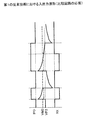
図26に第1の従来技術として電流パルス受信回路100を示す。光パルスはフォトダイオードPDで受光されて電流パルスIPDに変換される。電流パルスIPDは、電流電圧変換回路101Aの入力ノードINに入力されて電圧に変換され増幅回路102Aの反転入力端子VM2に出力される。ここでは、電流電圧変換回路101Aの入力端子をシングル入力として例示しているが、非入力端子をダミー端子として、あるいは相補な電流パルスを入力することにより差動入力として構成することもできる。DCキャンセル回路105Aは、電流電圧変換回路101Aの出力信号VM2の直流電圧レベルを検出して、電流電圧変換回路101Aの入力ノードINにフィードバックすることにより、フォトダイオードPDで電流変換される太陽光、照明光等の直流的な外乱光をキャンセルする回路である。入力光パルスに対して時定数を十分に大きく設定することにより、入力周波数が数kHz以下の外乱光成分のみををキャンセルするものである。電流電圧変換回路101Aの差動入力に対応してDCキャンセル回路105Aを差動出力とする構成をとる場合もある。
【0006】
電流電圧変換回路101Aにより電圧に変換されたパルス信号は、増幅回路102Aに入力され増幅される。増幅することにより後段の比較回路103での応答性を良好なものにする働きを有する。増幅回路102Aの参照電圧端子VP2には、DCフィードバック回路106が入力されている。DCフィードバック回路106は、増幅回路102Aの出力端子VP3の電圧を積分回路C101、R101、R102により積分した上で増幅回路102Aの参照電圧端子VP2にフィードバックしており、増幅回路102Aにおける入力オフセット電圧を改善すると共に、反転入力端子VM2への信号入力の変化に遅れて追従することから入力端子間のヒステリシス効果を付加する機能を有している。
【0007】
増幅回路102Aからの出力は出力端子VP3を介して比較回路103に入力され、参照電圧端子VM3に接続される基準電圧VTHとの比較により正の論理パルスが出力される。この正の論理パルスはインバータ回路104にて反転され、電流パルス受信回路100の出力として出力端子RXから負の論理パルスを出力する。
【0008】
図27には、第2の従来技術として電流パルス受信回路200を示す。基本的な回路構成は図26に示す電流パルス受信回路100と同様である。電流パルス受信回路200では、電流電圧変換回路101Bからの出力信号を差動信号として、容量素子C102、C103を介して増幅回路102Bの入力端子に容量結合させることにより、増幅回路102Bにおける入力オフセット電圧を改善している。このため、DCキャンセル回路105Bも差動入力構成をとっている。
電流パルス受信回路100と同様に、DCキャンセル回路105Bにより外乱光による直流的なオフセットをキャンセルする。また、増幅回路102Bの入力端子への容量結合により増幅回路102Bの入力オフセット電圧を改善すると共に、差動信号の入力により入力信号間には有意な電位差が付加される。
【0009】
【発明が解決しようとする課題】
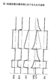
しかしながら、IrDA通信等の光通信におけるバースト信号に伴う広狭様々な光パルス幅に加えて、フォトダイオードPDの出力特性から決まる電流出力のテール特性や、パルス信号の微分波形におけるテール特性等の違いにより、電流出力のテール領域においても比較回路103での誤出力が発生しない十分なヒステリシス電圧幅を安定に設定することが困難である。即ち、出力電流におけるテール特性の異なるフォトダイオードPDに対しては設定値がずれてしまう。また、微分波形についても、フォトダイオードPDや微分回路の定数、入力信号振幅によりテール領域は変化してしまう。更に、受光する光パルスの強度、電流パルスIPDのクランプレベル等の様々な条件によりテール領域の発生の仕方は異なることとなる。従って、使用部品の特性、微分回路等の回路定数、及び使用環境等に依存してテール特性が変化してしまい、パルス幅の長い光パルスに対して精度の良い出力パルス幅を安定して出力することが困難であるという問題がある。
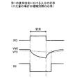
具体例として、図28に第1従来技術における比較回路103の応答の入出力波形を示す。この場合は、増幅回路102Aの出力がシングル出力で正転入力端子VP3に供給されており、基準電圧VTHから所定のヒステリシス電圧幅を有する信号が参照電圧端子VM3に供給されている。所定ヒステリシス電圧幅に対して、短い電流パルスIPDではパルス幅の精度よく出力信号RXが出力される。しかしながら、長い電流パルスIPDでは微分波形である比較回路103への入力信号VP3がテールを引くため、入力電流パルスIPD幅の途中で比較回路103の入力関係が逆転し、出力信号RXが反転してしまう。図29には、第2従来技術におけるコンパレータ103の応答の入出力波形を示す。この場合は、増幅回路102Bの出力が差動出力で各入力端子VP3、VM3に供給されている。差動信号であるため、短い電流パルスIPDではパルス幅の精度よく出力信号RXが出力される。しかしながら、差動信号は共に微分波形でありテールを引くため、長い電流パルスIPDでは入力電流パルスIPD幅の途中で比較回路103の入力関係が逆転し、出力信号RXが反転してしまう。
図28に示すようなシングル入力の信号に対して基準電圧VTHに所定ヒステリシス電圧幅を付加する場合には、ヒステリシス電圧幅を大きく設定すれば改善することはできる。しかしながら、小入力信号時の振幅以上にヒステリシス電圧幅を大きく設定すると、セットされたヒステリシス電圧を解除することができなくなり、出力端子RXがセットされたままロックしてしまう虞があり問題である。
【0010】
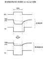
また、光パルスが大光量で入力される場合には、電流電圧変換回路101A、101Bにおいて出力電圧振幅をクランプする。この場合のクランプ動作は、バイポーラトランジスタやダイオード等における接合の順方向電圧を利用することが一般的であるため、クランプ動作時の出力電圧振幅を接合の順方向電圧以下に設定することができない。そのため、小光量時における出力電圧振幅との差が大きくなりすぎてしまい、小光量時に比して大光量時のパルス終端でのフォトダイオードPD特性によるテール波形が顕著になる。そのため、大光量時においてパルス終端を正確に検出することができず、出力端子RXのパルス幅が実際の幅に比して大きくなってしまうという問題がある。
具体例として、図30に第1従来技術の場合の増幅回路102Aの応答波形を、図32に第2従来技術の場合の増幅回路102Bの応答波形を示す。何れの場合にも、パルス波形VM2の終端においてフォトダイオードPDの出力特性に起因するテール波形が顕著となり、参照電圧VP2(図30の場合)、あるいは相補電圧VP2(図32の場合)との交点が実際の光パルスの終端に比して遅れる結果となり、出力端子RXのパルス幅が大きくなってしまう。
【0011】
更に、光パルスが小光量で入力される場合には、クランプ動作を受けることなくフォトダイオードPDの出力特性がそのまま出力されるため、パルスの始端及び終端の双方においてテール波形が顕著となる。但し、パルス始端においては、入力信号間の電位差が広がる方向であるため出力端子RXにおけるパルス始端には、応答の遅れはない。しかしながら、パルス終端においては、テール波形が入力信号の交差を遅らせる方向に作用するため上述の大光量の場合と同様に、パルス終端を正確に検出することができず、出力端子RXのパルス幅が実際の幅に比して大きくなってしまうという問題がある。
具体例として、図31に第1従来技術の場合の増幅回路102Aの応答波形を、図33に第2従来技術の場合の増幅回路102Bの応答波形を示す。何れの場合にも、パルス波形VM2の終端においてフォトダイオードPDの出力特性に起因するテール波形により、参照電圧VP2(図31の場合)、あるいは相補電圧VP2(図33の場合)との交点が実際の光パルスの終端に比して遅れる結果となり、出力端子RXのパルス幅が大きくなってしまう。
【0012】
赤外線領域も含めたIrDA通信等の光通信においては、送受信される光パルス信号は、一般にバースト信号であり、パルス幅及びデューティ比が変化する信号である。更に送信される光の強度は、光パルス信号の伝送距離や伝送環境により光強度が大きく変化する。従って、上記に示すパルス幅の変化や光強度の変化に対して、正確なパルス幅を出力することができないという問題がある。
【0013】
本発明は前記従来技術の問題点を解消するためになされたものであり、光通信等において受光した光パルスを受光素子により変換した電流パルスを、パルス幅の精度よく論理レベルの電圧パルスに変換して出力する電流パルス受信回路を提供することを目的とする。
【0014】
【課題を解決するための手段】
前記目的を達成するために、請求項1に係る電流パルス受信回路は、入力電流パルスを電圧パルスに変換する電流電圧変換部と、その出力信号と、出力信号と相補な信号あるいは基準電圧とを比較して、論理信号パルスを出力する比較回路と、論理信号パルスに基づき比較回路の入力信号に、第1所定幅のヒステリシス電圧を設定する第1ヒステリシス回路と、第2所定幅から時間経過と共に減少するヒステリシス電圧を設定する第2ヒステリシス回路とを備えることを特徴とする。
【0015】
請求項1の電流パルス受信回路では、電流電圧変換部により入力電流パルスを電圧パルスに変換した後、比較回路において論理信号パルスを出力する際、論理信号パルスに基づいて、入力信号に、第1ヒステリシス回路による第1所定幅のヒステリシス電圧に加え、第2ヒステリシス回路による第2所定幅から時間経過と共に減少するヒステリシス電圧を重畳する。
【0016】
これにより、入力電流パルスから変換された電圧パルスにおける最大パルス幅に対して十分なヒステリシス電圧幅を有するように、第1ヒステリシス回路により設定されるヒステリシス電圧の第1所定幅と、第2ヒステリシス回路により設定される第2所定幅及び時間経過に伴う減少割合とを設定すれば、全てのパルス幅の電圧パルスに対して十分なヒステリシス電圧幅を設定することができる。従って、IrDA通信等の光通信に応用した場合、バースト信号に伴う広狭様々な光パルス幅に加えて、光パルスを電流パルスに変換するフォトダイオードの出力特性やパルス信号の微分波形におけるテール特性等の違いを吸収して、テール領域においても比較回路において誤出力が発生しない十分なヒステリシス電圧幅を安定して設定することができる。そして、特に第2ヒステリシス回路における第2所定幅及び時間経過に伴う減少割合の設定に応じて定まる最長パルス幅のパルス範囲で精度の良い出力パルス幅を安定して出力することができる。最長の入力光パルス幅が決まっているIrDA通信等の光通信における受信回路に使用して好適なものである。
また、ヒステリシス電圧幅は、設定直後には第1所定幅と第2所定幅との和のヒステリシス電圧幅を有しながら、時間経過と共に減少していき最終的には、第1所定幅にまで減少する。従って、第1所定幅を小振幅入力信号の振幅以下に設定することにより、セットされたヒステリシス電圧が解除することができず出力端子がセットされたままロックしてしまう虞を未然に回避することができる。
【0017】
また、請求項2に係る電流パルス受信回路は、請求項1に記載の電流パルス受信回路において、電流電圧変換部からの出力信号の電圧振幅を制限して比較回路に出力する電圧振幅制限回路を備えることを特徴とする。
【0018】
請求項2の電流パルス受信回路では、電圧振幅制限回路により、比較回路への入力信号の電圧振幅が制限される。
【0019】
これにより、電圧振幅制限回路により、電流電圧変換部からの大振幅信号の電圧振幅が制限され小振幅信号との電圧振幅差が圧縮され、比較回路への入力信号範囲が制限される。従って、第1ヒステリシス回路による第1所定幅と、第2ヒステリシス回路による第2所定幅とにより設定される固定値であるヒステリシス電圧幅によるヒステリシス効果を常に一定にすることができる。即ち、小振幅信号から大振幅信号に至るまで、確実かつ有効にヒステリシス効果を付与することができ、入力信号のテール特性等の違いを吸収して、テール領域においても比較回路において誤出力が発生せず精度のよいパルス幅を安定して出力することができる。
また、比較回路への入力信号範囲が制限されるため、同一のヒステリシス特性の設定に対して、より長いパルス幅の電圧パルスにまで有効なヒステリシス効果を付与することができる。
【0020】
また、請求項3に係る電流パルス受信回路は、請求項1又は2に記載の電流パルス受信回路において、比較回路への入力信号のオフセット値を設定するオフセット設定回路を備えることを特徴とする。
【0021】
請求項3の電流パルス受信回路では、オフセット設定回路により比較回路への入力信号のオフセット値を設定する。
【0022】
これにより、比較回路への入力信号のオフセット値を所望の値に設定できるので、入力信号のパルス幅や電圧振幅、またテール特性、更にはノイズ環境等に合わせて、最適なオフセット値を設定することができ、誤動作がなく精度の良いパルス幅を安定して出力することができる。
また、オフセット設定回路におけるオフセットの設定を外部調節できるように構成すれば、使用環境に合わせてオフセット値を適宜変更することができ、更に安定した電流パルス受信回路を実現することができる。
【0023】
また、請求項4に係る電流パルス受信回路は、請求項1乃至3の少なくとも何れか1項に記載の電流パルス受信回路において、比較回路への入力信号の供給を行なう第1バッファ回路と、第1バッファ回路の入力端子へ入力信号の供給を行なう容量結合用の容量結合素子と、第1バッファ回路の入力端子と所定電位との間に接続されるバイアス抵抗素子と、容量結合素子を介して第1バッファ回路へ入力信号を供給する電圧振幅制限回路と、電流電圧変換部の出力信号における高電位側出力電圧をホールドするピークホールド回路、あるいは出力信号を積分する積分回路と、これらの出力電圧に基づき、電圧振幅制限回路の低電位側出力電圧を所定電圧だけ上昇させる低電位レベル上昇回路とを備えることを特徴とする。
【0024】
請求項4の電流パルス受信回路では、電流電圧変換部の出力信号が電圧振幅制限回路により電圧振幅の制限をされた後、容量結合素子を介して容量結合されて第1バッファ回路に入力され、比較回路への入力信号として供給される。更に、電流電圧変換部には、高電位側出力電圧をホールドするピークホールド回路、あるいは出力信号を積分する積分回路の出力端子が接続され、これらの出力電圧に基づき、低電位レベル上昇回路が電圧振幅制限回路の低電位側出力電圧を所定電圧だけ上昇させる。
【0025】
ピークホールド回路がない場合には、容量結合素子に接続される第1バッファ回路の入力端子のベースライン電位は、電圧振幅制限回路から容量結合されるパルス信号の電圧値の平均となり、この信号が第1バッファ回路を介して比較回路の入力信号となり、これが参照電圧ともなる。IrDA通信等において電圧振幅制限回路から出力される正の信号パルスのデューティが低い場合には、比較回路の入力信号電圧は、バースト信号の受信中に徐々に低下することとなる。この傾向は、電圧振幅制限回路からの出力信号が制限されている大振幅動作の場合に顕著に現れるので、大振幅のバースト信号により比較回路の入力信号が低下している状態からバースト信号の受信が終了して無信号状態に戻る際、入力信号のオーバーシュートがあると、低下している比較回路の参照電圧側の入力信号との間で電位関係が逆転して誤パルスを出力してしまう可能性がある。
そこで、ピークホールド回路、あるいは積分回路により、電流電圧変換部の出力信号を検出する。バースト信号が入力されると、ピークホールド回路、あるいは積分回路の出力電圧は上昇していき所定電位に達した時点で、低電位レベル上昇回路が電圧振幅制限回路の低電位側出力電圧を所定電圧だけ上昇させる。
これにより、電圧振幅制限回路の低電圧側出力は、出力期間が長く電圧振幅が小さくなるのに対して、高電圧側出力は、出力期間が短いが電圧振幅が不変のままとなり、信号電圧値の平均がバランスされる結果、比較回路の入力端子における電圧振幅の低下減少を解消することができ、大振幅動作からの復帰時に発生するオーバーシュートを含む波形のうねり現象が発生する場合にも比較回路が誤パルスを出力することがなくなる。従って、電圧振幅制限回路により、小振幅信号から大振幅信号に至るまで、確実かつ有効にヒステリシス効果を付与することができ、入力信号のテール特性等の違いを吸収して、テール領域においても比較回路において誤出力が発生せず精度のよいパルス幅を安定して出力することができることに加え、信号受信終了時における誤パルスの発生も防止することができ、精度のよいパルス幅を安定して出力することができる。
【0026】
また、請求項5に係る電流パルス受信回路は、請求項1乃至3の少なくとも何れか1項に記載の電流パルス受信回路において、比較回路への入力信号の供給を行なう第1バッファ回路と、第1バッファ回路の入力端子へ入力信号の供給を行なう容量結合用の容量結合素子と、第1バッファ回路の入力端子と所定電位との間に接続されるバイアス抵抗素子と、容量結合素子を介して第1バッファ回路へ入力信号を供給する電圧振幅制限回路と、電流電圧変換部の出力信号における高電位側出力電圧をホールドするピークホールド回路、あるいは出力信号を積分する積分回路と、これらの出力電圧に基づき、電流電圧変換部の電流電圧変換抵抗を調整する抵抗率自動調整回路とを備えることを特徴とする。
【0027】
請求項5の電流パルス受信回路では、電流電圧変換部の出力信号が電圧振幅制限回路により電圧振幅の制限をされた後、容量結合素子を介して容量結合されて第1バッファ回路に入力され、比較回路への入力信号として供給される。更に、電流電圧変換部には、高電位側出力電圧をホールドするピークホールド回路、あるいは出力信号を積分する積分回路が接続され、これらの出力電圧に基づき、抵抗率自動調整回路が電流電圧変換部の電流電圧変換抵抗を調整する。
【0028】
これにより、大振幅の入力電流パルスが入力されるときに、電流電圧変換部の電流電圧変換抵抗を調整して下げることができるので、電流電圧変換部の出力信号を小振幅信号とすることができる。従って、正パルスのデューティが低いIrDA通信等においても、容量結合された比較回路の入力信号のベースバンド電位に電圧低下は殆んど発生しない。また、信号の電圧振幅も小振幅信号の振幅レベルに低減されるので、バースト信号終了時の無信号状態への復帰においても、比較回路の入力信号にオーバーシュート等のうねりは発生しない。それゆえ、バースト信号終了後に比較回路が誤パルスを出力することはなく、入力電流パルスが小振幅から大振幅に至るまで、確実かつ有効にヒステリシス効果を付与することができ、入力信号のテール特性等の違いを吸収して、テール領域においても比較回路において誤出力が発生せず精度のよいパルス幅を安定して出力することができることに加え、信号終了時における誤パルスの発生も防止することができ、精度のよいパルス幅を安定して出力することができる。
【0029】
また、請求項6に係る電流パルス受信回路は、入力電流パルスを電圧パルスに変換する電流電圧変換回路と、その出力信号の電圧振幅が所定振幅以上であることを検出する大信号検出回路と、電流電圧変換回路における直流オフセット成分をキャンセルするDCキャンセル回路とを備え、大信号検出回路からの出力信号に基づき、DCキャンセル回路における直流オフセット成分のキャンセル効果を低減することにより電流電圧変換回路における電流電圧変換抵抗を低減して出力振幅のクランプレベルを低減することを特徴とする。
【0030】
請求項6の電流パルス受信回路では、電流電圧変換回路により入力電流パルスから変換された電圧パルスの電圧振幅が所定振幅以上であることを、大信号検出回路が検出した際、電流電圧変換回路における直流オフセット成分をキャンセルするDCキャンセル回路のキャンセル効果を、大信号検出回路からの出力信号に基づき低減することにより電流電圧変換回路における電流電圧変換抵抗を低減して出力振幅のクランプレベルを低減する。
【0031】
これにより、電流電圧変換回路からの出力信号の電圧振幅が所定振幅以上の大振幅信号であることを検出した際、電流電圧変換抵抗を低減するので、入力電流パルスにおける電流振幅の変化に対して出力電圧の電圧振幅の変化を低く抑制することができ、所定振幅以上の広い入力電流パルスの電流振幅範囲に対してパルス幅の精度よく電圧信号に変換することができる。更に、出力電圧振幅のクランプレベルを低減するので、最大の電圧振幅を制限することができ、大振幅の入力電流パルスに対してもパルス幅の精度良く電圧パルス信号に変換することができる。また、大信号検出回路からの出力信号に基づいて、DCキャンセル回路による電流電圧変換回路の直流オフセット成分のキャンセル効果を、低減することができる。
大振幅の入力電流パルスに対する出力電圧振幅も小さく制限されるため、出力電圧信号におけるテール波形が問題となることはなく、大振幅の入力電流パルスに対してもパルス終端を正確に検出することができ、パルス幅が精度よく出力される。
IrDA通信等の光通信における強弱様々な光パルス信号に加えて、光パルスを電流パルスに変換するフォトダイオードPDの出力特性やパルス信号の微分波形におけるテール特性等の違いを吸収して、入力光パルスのパルス幅に精度良く一致した出力パルス幅を安定して出力することができる。
【0032】
また、請求項7に係る電流パルス受信回路は、入力電流パルスを電圧パルスに変換する電流電圧変換回路と、電流電圧変換回路の出力信号の電圧振幅が所定振幅以上であることを検出する大信号検出回路と、大信号検出回路からの出力信号に基づき、電流電圧変換回路における電流電圧変換抵抗を、所定ゲインから対数関数ゲインに変換するゲイン変換部とを備えることを特徴とする。
【0033】
請求項7の電流パルス受信回路では、電流電圧変換回路により入力電流パルスから変換された電圧パルスの電圧振幅が所定振幅以上であることを、大信号検出回路が検出した際、ゲイン変換部により電流電圧変換回路における電流電圧変換抵抗を、所定ゲインから対数関数ゲインに変換する。
【0034】
これにより、請求項6の場合と同様に、電流電圧変換回路からの出力信号の電圧振幅が所定振幅以上の大振幅信号であることを検出した際、入力電流パルスにおける電流振幅の変化に対して出力電圧の電圧振幅の変化を低く抑制することができ、所定振幅以上の広い入力電流パルスの電流振幅範囲に対してパルス幅の精度よく電圧信号に変換することができる。
【0035】
また、請求項8に係る電流パルス受信回路は、請求項6又は7に記載の電流パルス受信回路において、電流電圧変換回路は、電流電圧変換抵抗素子を備えており、クランプ回路は、バイアス回路と、電流電圧変換抵抗素子と並列に接続されて大信号検出回路からの出力信号に基づきバイアス回路により導通状態にバイアスされる、エミッタフォロアトランジスタあるいはダイオードとを備えることを特徴とする。
【0036】
請求項8の電流パルス受信回路では、電流電圧変換抵抗素子を備えた電流電圧変換回路は、電流電圧変換抵抗素子と並列に接続されエミッタフォロアトランジスタあるいはダイオードを、大信号検出回路からの出力信号に基づいてバイアス回路により導通状態にバイアスする。
【0037】
これにより、大信号検出回路からの出力信号に基づいてエミッタフォロアトランジスタ等を導通状態とするようにバイアス回路を設定することができるので、エミッタトランジスタ等の導通電流を、順方向接合電圧の対数特性にすることができ、電流電圧変換回路の電流電圧変換抵抗を容易に低減することができる。また、エミッタトランジスタ等が導通状態となることにより出力抵抗を小さくすることができ、電流電圧変換回路の出力電圧振幅のクランプレベルを容易に低減することができる。
【0038】
また、請求項9に係る電流パルス受信回路は、請求項8に記載の電流パルス受信回路において、バイアス回路は、エミッタフォロアトランジスタあるいはダイオードの温度特性を抑制する温度特性を有することを特徴とする。
【0039】
請求項9の電流パルス受信回路では、バイアス回路の温度特性により、エミッタフォロアトランジスタあるいはダイオードの温度特性を抑制する。
【0040】
これにより、エミッタフォロアトランジスタ等の温度特性が、バイアス回路の温度特性により抑制されるので、高温におけるエミッタフォロアトランジスタ等のリーク電流特性の悪化を防止することができ、広い温度範囲において、一定の電流電圧変換抵抗の低減効果と、出力電圧振幅のクランプレベルの低減効果を得ることができる。
【0041】
また、請求項10に係る電流パルス受信回路は、入力電流パルスを電圧パルスに変換する電流電圧変換回路と、その出力信号に基づいて増幅動作を行う差動入力構成の増幅回路と、電流電圧変換回路と増幅回路との間に挿入される一対の差動出力構成のバッファ回路とを備え、一対のバッファ回路の各々の正転出力端子を、容量素子を介して増幅回路の差動入力端子に接続すると共に、一対のバッファ回路のうち一方の反転出力端子を、容量素子で構成される微分回路を介して、一対のバッファ回路のうち他方の入力端子に接続することを特徴とする。
【0042】
請求項10の電流パルス受信回路では、電流電圧変換回路において、入力電流パルスから電圧パルスに変換された出力信号を、一対の差動出力構成のバッファ回路を介して差動入力構成の増幅回路に入力する。そして、容量素子で構成される微分回路により、一対のバッファ回路のうち一方の反転出力を微分して、一対のバッファ回路のうち他方の入力端子に供給する。
【0043】
これにより、パルス信号の反転信号が微分され、パルス信号の遷移部分に急峻な微分波形を有する信号が増幅回路の他方の入力信号ラインに入力される。微分信号が入力されるノードは高インピーダンスのノードであるので、微分信号は確実に重畳される。この信号と入力パルス信号とが増幅回路に入力され、パルス信号の遷移部においてパルス信号を強調する側にヒステリシス効果を付与することとなる。
従って、パルス遷移部のなまった電流パルスが入力される場合においても、反転信号の微分波形をもってヒステリシス波形とするので、ヒステリシス効果を十分に得ることができ、パルス幅の精度よくパルス出力をすることができる。
IrDA通信等の光通信において、小振幅の光パルスが入力された場合に、フォトダイオード等の出力特性が顕著に現れて電流パルスの遷移部がなまった場合においても、精度のよいパルス幅の出力を得ることができる。
【0044】
また、請求項11に係る電流パルス受信回路は、入力電流パルスを電圧パルスに変換する電流電圧変換回路と、電流電圧変換回路からの出力信号に基づいて増幅動作を行う差動入力構成の増幅回路と、電流電圧変換回路と増幅回路との間に挿入され、増幅回路への各入力信号を供給する一対の差動出力構成のバッファ回路と、一対のバッファ回路の各反転出力を微分し、他方のバッファ回路の各入力端子に供給する一対の微分回路とを備えることを特徴とする。
【0045】
請求項11の電流パルス受信回路では、一対のバッファ回路と、一対の微分回路とが増幅回路に対して対称に配置されて、相互に微分波形を重畳する。
【0046】
これにより、増幅回路の各入力端子における回路の対称性が確保されるため、各入力端子に至る信号経路における負荷、ノイズ等の外乱、電源電圧の変動等は、両信号経路に同等に作用することとなるので、これらの変動に対しても安定した動作を確保することができる。
【0047】
【発明の実施の形態】
以下、本発明の電流パルス受信回路について具体化した第1乃至第9実施形態を図1乃至図25に基づき図面を参照しつつ詳細に説明する。
図1は、第1実施形態の電流パルス受信回路を示す回路ブロック図である。図2は、第1実施形態における比較回路への入力がシングル入力の場合の入出力波形である。図3は、第1実施形態における比較回路への入力が差動入力の場合の入出力波形である。図4は、第1実施形態の電流パルス受信回路の具体例を示す回路図である。図5は、第1実施形態の電流パルス受信回路の具体例における入出力波形である。図6は、第2実施形態の電流パルス受信回路を示す回路図である。図7は、第2実施形態の電流パルス受信回路における入出力波形である。図8は、第3実施形態の電流パルス受信回路を示す回路図である。図9は、第4実施形態の電流パルス受信回路を示す回路図である。図10は、第4実施形態の電流パルス受信回路における入出力波形である。図11は、第5実施形態の電流パルス受信回路を示す回路図である。図12は、第5実施形態の電流パルス受信回路における入出力波形である。図13は、第6実施形態の電流パルス受信回路の第1具体例を示す要部回路図である。図14は、電流電圧変換回路の具体例を示す回路図である。図15は、第6実施形態の電流パルス受信回路における大信号検出回路と電流電圧変換回路特性の関係を示す波形である。図16は、第6実施形態の電流パルス受信回路の第1具体例における入出力波形である。図17は、第6実施形態の電流パルス受信回路の第2具体例を示す回路ブロック図である。図18は、第6実施形態の電流パルス受信回路の第2具体例における入出力波形である。図19は、第7実施形態の電流パルス受信回路における電流電圧変換回路の温特キャンセル用バイアス回路を示す回路図である。図20は、第8実施形態の電流パルス受信回路を示す回路ブロック図である。図21は、第8実施形態の増幅回路への入力が差動入力の場合の入出力波形である。図22は、第8実施形態の増幅回路への入力がシングル入力の場合の入出力波形である。図23は、第8実施形態の電流パルス受信回路の具体例を示す回路図である。図24は、第9実施形態の電流パルス受信回路を示す回路ブロック図である。図25は、第9実施形態の電流パルス受信回路の具体例を示す回路図である。
【0048】
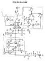
図1に示す第1実施形態の電流パルス受信回路1の回路ブロック図は、入力される光パルスをフォトダイオードPDにより電流パルスIPDに変換した上で、電流電圧変換回路101Aにより電圧パルスに変換し、増幅回路102により増幅した後に、比較回路103で論理信号パルスに変換し、更にインバータ104にて反転して出力端子RXより負の論理パルスを出力する基本的構成は、第1及び第2従来技術における構成と同様である。図1では、説明の便宜上、DCキャンセル回路105A、105B、及びDCフィードバック回路106を省略している。また、電流電圧変換回路101Aと増幅回路102との接続を容量素子C1で容量結合した構成として例示しているが、実際の回路構成はこの接続に限定されるものではなく、従来技術に示したように、単層の直接接続(第1従来技術の場合)でも差動の容量結合接続(第2従来技術の場合)でも第1実施形態として実現可能である。更に、増幅回路102と比較回路103との接続についても、図1に示すように容量素子C2による単層の容量結合でも図1中の点線で示すように、容量素子C3を追加して差動の容量結合とすることもできる。更に容量結合させずに直結することもできる。
【0049】
第1実施形態の電流パルス受信回路1では、比較回路103への入力信号VP3に対して参照電圧信号VM3にヒステリシス電圧を印加するに際し、比較回路103の出力端子のパルス出力に伴い、直流的なヒステリシスを付与するDCヒステリシス回路11に加えて、所定初期幅から時間と共に減少するヒステリシス電圧幅を出力することができるACヒステリシス回路12を追加している。
【0050】
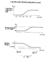
図2、3には、これらの2つのヒステリシス回路11、12が奏する効果を比較回路103の入出力応答波形として示している。図2は、比較回路への入力信号がシングル入力であり他方の入力端子が基準電圧VTHに固定された参照電圧端子である場合である。図2から明らかなように、光パルスの受光に伴いフォトダイオードPDから電流パルスIPDが出力されると、電流電圧変換回路101Aから増幅回路102を経て増幅された電圧パルスが、経路途中の容量素子C1、C2により微分された状態で比較回路103の入力端子VP3に印加される。印加されると同時に比較回路103の出力端子にパルス信号が出力され、インバータ104を介して更に反転されて出力端子RXが負側に反転する。これと同時に比較回路103の出力反転を受けてDC及びACヒステリシス回路11、12が動作を開始し、比較回路の参照電圧端子VM3の電圧を大きく反対方向に振って入力信号間にヒステリシス電圧を印加する。このときのヒステリシス電圧は、固定電圧幅を有するDCヒステリシス回路11からの電圧に加算される形で、ACヒステリシス回路12からの電圧が重畳される。従って、ヒステリシス電圧印加の直後から、参照電圧端子VM3の電圧は、時間経過と共に徐々に電圧幅を減少させていく。そして、短いパルスではヒステリシス電圧幅の減少途中でパルス期間が終了することとなり、パルス幅が長くなるに従いパルス終端での残留ヒステリシス電圧幅は減少していく。最長パルス幅におけるパルス終端で、比較回路103の誤出力を防止できるのに十分なヒステリシス電圧幅が残留するようにACヒステリシス回路12によるヒステリシス電圧幅の減少割合を設定しておけば、全てのパルス幅において十分なヒステリシス電圧幅をもって比較回路103が動作することとなる。
【0051】
図3は、比較回路への入力信号が差動入力の場合である。この場合にも反転入力端子VM3にDC及びACヒステリシス回路11、12を接続してやれば、パルス出力中の比較回路103における入力信号間のヒステリシス電圧幅を誤パルスが出力することのない程度に十分に設定してやることにより、図2の場合と同様に、全てのパルス幅において十分なヒステリシス電圧幅をもって比較回路103が動作することとなる。
【0052】
図4は、第1実施形態の具体的な回路図例を示している。増幅回路102の出力端子は、容量結合用の容量素子C2を介してバッファ回路を構成するエミッタフォロアトランジスタQ1のベース端子に入力される。エミッタフォロアトランジスタQ1のエミッタ端子は、抵抗素子R3を介して比較回路103の入力端子VP3に接続される。一方、参照電圧側は、入力信号側と同じバッファ回路構成をとるエミッタフォロアトランジスタQ2のエミッタ端子から抵抗素子R4を介して比較回路103の参照電圧端子VM3に接続される。そして、参照電圧端子VM3は、無信号時、基準電圧VREFからベース・エミッタ間の順方向電圧VBEを減じたVREF−VBEの参照電圧が印加されている。ここで、エミッタフォロアトランジスタQ2のベース端子は、入力信号側とのバランスをとるため、抵抗素子R1及び容量素子C2と同一構成、同一サイズである抵抗素子R2及び容量素子C3に接続されている。図4における具体例では、増幅回路102がシングル出力である場合を示しているが、これを差動出力にした場合も同様に構成することができる。差動出力の場合には、反転出力信号の端子A1を容量素子C3の端子A1に接続すればよい。また、図4では、バッファ回路をNPNバイポーラトランジスタQ1、Q2で構成した場合を示しているが、これに限定される必要はなく、NMOSトランジスタを使用しても、更に、電位関係の極性を反転させれば、PNPバイポーラトランジスタやPMOSトランジスタ等を使用して構成できることはいうまでもない。
【0053】
さて、ヒステリシス回路は、図中11及び12として指示される部分である。先ず、DCヒステリシス回路11は、定電流源回路I3をNMOSトランジスタM1で開閉して構成される。NMOSトランジスタM1のゲート端子には、比較回路103の出力端子が接続されており、パルスが入力され出力端子が正に反転することによりオンする。このトランジスタM1のオンにより、定電流源回路I3が参照電圧端子VM3に接続されて、定電流I3が電流IDCとしてエミッタフォロアトランジスタQ2から抵抗素子R4を介して流れることにより、抵抗素子R4にR4×IDCの電圧ドロップが生じヒステリシス電圧が発生する。電流IDCは比較回路103の出力端子が正に反転中は、定電流I3に固定されるため、R4×IDCのヒステリシス電圧は直流的な電圧となる。
【0054】
ACヒステリシス回路12は、2つのNMOSトランジスタM4、M5により電流分流回路が構成され、NMOSトランジスタM2により定電流源回路I4が接続されて定電流I4を分流する。NMOSトランジスタM4は、ゲート端子に印加される基準電圧VREFにより所定のオン抵抗を持って導通されており、定電流源回路I4を比較回路103の参照電圧端子VM3に接続している。NMOSトランジスタM5は、電源電圧+Vに接続されている。ゲート端子VXには、接地電位との間で容量素子C4が接続されると共に、容量素子C4への充電パスとして定電流源回路I5が、放電パスとしてNMOSトランジスタM3が接続されている。比較回路103の出力端子からの信号は、インバータ31に入力され、反転されてNMOSトランジスタM3に入力されると共に、インバータ32で再反転されてNMOSトランジスタM2に入力される。
【0055】
比較回路103の出力端子が正に反転すると、インバータ31の出力端子が負に、インバータ32の出力端子が正に反転するので、NMOSトランジスタM3はオフし、NMOSトランジスタM2はオンする。初期の状態では、ゲート端子VXは十分に放電されており、NMOSトランジスタM5がオフ状態で、分流回路に定電流源回路I4が接続される。定電流I4はNMOSトランジスタM4を介して電流IACとして抵抗素子R4を流れ、抵抗素子R4にR4×IACのヒステリシス電圧が重畳される。その後は、ゲート端子VXの電位が、容量素子C4への定電流I5による充電につれて徐々に上昇していき、NMOSトランジスタM5のオン抵抗が徐々に下がる。そのため定電流I4は徐々にNMOSトランジスタM5側に分流していき電流IACは徐々に減少していく。最終的には、ゲート端子VXの電圧が電源電圧+Vにまで上昇することから、NMOSトランジスタM5のオン抵抗がNMOSトランジスタM4のオン抵抗より小さくなり、定電流I4はNMOSトランジスタM5を流れることとなる。従って、R4×IACのヒステリシス電圧は、R4×I4から0まで徐々に減少する交流的な電圧となる。
【0056】
図5に比較回路103における入出力波形を示す。図2において既に説明したように、短い電流パルスに対しても長い電流パルスに対しても十分なヒステリシス電圧幅が付与されるため、比較回路103において誤パルスが発生することはなく、出力端子RXに精度のよいパルス幅が出力される。
【0057】
これにより、入力電流パルスIPDから変換された電圧パルスにおける最大パルス幅に対して十分なヒステリシス電圧幅を有するように、第1ヒステリシス回路11により設定されるヒステリシス電圧の第1所定幅と、第2ヒステリシス回路12により設定される第2所定幅及び時間経過に伴う減少割合とを設定すれば、全てのパルス幅の電圧パルスに対して十分なヒステリシス電圧幅を設定することができる。従って、IrDA通信等の光通信に応用した場合、バースト信号に伴う広狭様々な光パルス幅に加えて、光パルスを電流パルスIPDに変換するフォトダイオードPDの出力特性やパルス信号の微分波形におけるテール特性等の違いを吸収して、テール領域においても比較回路103において誤出力が発生しない十分なヒステリシス電圧幅を安定して設定することができる。そして、特に第2ヒステリシス回路12における第2所定幅及び時間経過に伴う減少割合の設定に応じて定まる最長パルス幅のパルス範囲で精度の良い出力パルス幅を安定して出力することができる。最長の入力光パルス幅が決まっているIrDA通信等の光通信における受信回路に使用して好適なものである。
また、ヒステリシス電圧幅は、設定直後には第1所定幅と第2所定幅との和のヒステリシス電圧幅を有しながら、時間経過と共に減少していき最終的には、第1所定幅にまで減少する。従って、第1所定幅を小振幅入力信号の振幅以下に設定することにより、セットされたヒステリシス電圧が解除することができず出力端子がセットされたままロックしてしまう虞を未然に回避することができる。
【0058】
尚、図4の具体例では、交流的なヒステリシス電圧を実現するために定電流I4を時間経過と共に分流していく構成について示したが、他の方法で実現することも可能である。例えば、定電流源回路I4の出力電流値I4が時間と共に減少していく構成とすることができる。これは、定電流源回路I4における定電流I4を生成する抵抗素子をMOSトランジスタ等の能動抵抗素子として、抵抗値を制御する制御電圧を時間と共に変化させたり、電圧源の電圧値自身を経時的に減少させることで可能である。また、定電流I4のパスにMOSトランジスタ等の能動抵抗素子を挿入しておき、制御電圧により経時的に抵抗値を増大させることでも可能である。また、その他の構成例として、抵抗素子R4をMOSトランジスタ等の能動抵抗素子として、制御電圧により経時的に抵抗値を減少させるようにすることもできる。
【0059】
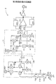
図6に示す第2実施形態の電流パルス受信回路2の回路図は、第1実施形態の電流パルス受信回路1に、増幅回路102の出力電圧振幅を制限する電圧振幅制限回路13Aを追加した構成である。増幅回路102の出力信号は容量素子C2により容量結合されてNMOSトランジスタM6のゲート端子に入力されている。このゲート端子は、基準電圧VREFから抵抗素子R5を介して直流的にバイアスされている。ここに、抵抗素子R5は、直流バイアス用であると共に、容量素子C2との組合わせでハイパスフィルタ回路の構成を採っており、カットすべき低域ノイズの周波数を決定する機能をも兼ねるものである。
NMOSトランジスタM6は、NMOSトランジスタM7と共に差動増幅対を構成している。抵抗素子R7、R8はそれぞれのトランジスタM6、M7の負荷抵抗であり、定電流源回路I7によりバイアスされる。NMOSトランジスタM7のゲート端子には抵抗素子R6を介して基準電圧VREFが印加されているが、NMOSトランジスタM6のゲート端子とのバランスをとるため、接地電位との間に容量素子C3が備えられている。第2実施形態では、増幅回路102からのシングル出力構成について例示しているが、差動出力とした場合も反転出力端子A2を容量素子C3の端子A2に接続することで構成することができる。
この差動増幅対の出力は、NMOSトランジスタM7と負荷抵抗R8との接続点から、定電流源回路I8でバイアスされたエミッタフォロアトランジスタQ3により取り出される。ここで、トランジスタQ3及び定電流源回路I8は、第1実施形態のトランジスタQ1及び定電流源回路I1に代わるものであり、参照電圧側のトランジスタQ2及び定電流源回路I2と、回路構成上バランスした構成となっている。
【0060】
無信号時の電圧振幅制限回路13Aの出力電圧(抵抗素子R3を介した入力端子VP3と同一電位となる。)は、差動増幅対がバランスした状態であるため抵抗素子R8に定電流I7の半分が流れることから、
VP3=VREF−R8×I7/2−VBE
となる。パルス入力時には、トランジスタM6のゲート端子へのバイアスが大きくなり、差動増幅対の入出力特性で決まる出力電圧として、
VP3(MAX)=VREF−VBE
を最大電圧として電圧出力される。パルス終了時には、トランジスタM7のゲート端子へのバイアスが大きくなり、
VP3(MIN)=VREF−R8×I7−VBE
を最小電圧とする電圧が出力される。即ち、電圧振幅制限回路13Aの出力電圧振幅は、
ΔVP3=VP3(MAX)−VP3(MIN)
=R8×I7
となる。増幅回路102から出力されるダイナミックレンジの広い出力信号は、差動増幅対の入出力特性によりΔVP3=R8×I7の狭い電圧範囲に限定されて出力されることとなる。そして、抵抗素子R8(合わせてR7も同様に変更する。)や定電流I7の値を適宜に設定することにより、所望の電圧振幅が得られる。
【0061】
図7に比較回路103における入出力波形を示す。入力端子VP3への入力信号振幅をΔVP3=R8×I7という狭い振幅幅に限定するので、DC及びACヒステリシス回路11、12によるヒステリシス効果を常に一定にすることができる。即ち、小光量パルスである小信号時においても、大光量パルスである大信号時においても、比較回路103の入力端子VP3、VM3において、常に一定のヒステリシス効果が得られ、比較回路103において誤パルスが発生することなく、出力端子RXに精度のよいパルス幅が出力される。
【0062】
これにより、電圧振幅制限回路13Aにより、電流電圧変換部101A、102からの大振幅信号の電圧振幅が制限され小振幅信号との電圧振幅差が圧縮され、比較回路103への入力信号範囲が制限される。従って、第1ヒステリシス回路11による第1所定幅と、第2ヒステリシス回路12による第2所定幅とにより設定される固定値であるヒステリシス電圧幅によるヒステリシス効果を常に一定にすることができる。即ち、小振幅信号から大振幅信号に至るまで、確実かつ有効にヒステリシス効果を付与することができ、入力信号のテール特性等の違いを吸収して、テール領域においても比較回路103において誤出力が発生せず精度のよいパルス幅を安定して出力することができる。
また、比較回路103への入力信号範囲が制限されるため、同一のヒステリシス特性の設定に対して、より長いパルス幅の電圧パルスにまで有効なヒステリシス効果を付与することができる。
【0063】
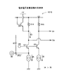
図8に示す第3実施形態の電流パルス受信回路3の回路図は、第2実施形態の電流パルス受信回路2に対して、オフセット設定機能付バッファ回路14を追加した構成である。第3実施形態では、増幅回路102Bと電圧振幅制限回路13Bとを直結し、電圧振幅制限回路13Bとオフセット設定機能付バッファ回路14との間に容量結合用容量素子C5を備えた構成である。
【0064】
オフセット設定機能付バッファ回路14は、第1実施形態においてバッファ回路として比較回路103に入力信号、参照電圧を供給するトランジスタQ1及び定電流源回路I1、トランジスタQ2及び定電流源回路I2(図4、参照)に代えて備えられたものである。
容量素子C5からの信号は、ソースフォロアトランジスタM8のゲート端子に入力されている。このゲート端子は、基準電圧VREFから抵抗素子R9を介して直流的にバイアスされている。ここに、抵抗素子R9は、直流バイアス用であると共に、容量素子C5との組合わせでハイパスフィルタ回路の構成をとっており、カットすべき低域ノイズの周波数を決定する機能をも兼ねるものである。
トランジスタM8のソース端子は、ショットキーダイオードD1のカソード端子に接続されると共に、抵抗素子R11を介して定電流源回路I9に接続されている。そして抵抗素子R11と定電流源回路I9との接続点が比較回路103の入力端子VP3となる。ショットキーダイオードD1のアノード端子は、抵抗素子R13を介して比較回路103の参照電圧端子VM3に接続されており、更に、参照電圧VTH設定回路としてソースフォロアトランジスタM9、抵抗素子R12、及び定電流源回路I10が、入力信号側のトランジスタM8、抵抗素子R11、及び定電流源回路I9とバランスして構成されている。加えて、トランジスタM9のゲート端子もトランジスタM8のゲート端子とバランスするように、抵抗素子R10と容量素子C6とにより構成されている。
【0065】
定常状態においては、トランジスタM8側とM9側とはバランスしているので、両者の対応端子は同電位となっている。そこでショットキーダイオードD1には電流は流れない。従って、トランジスタM8との接続点である抵抗素子R11の端子電位は、比較回路103の参照電圧端子VM3と同電位となる。抵抗素子R11の他方の端子は比較回路103の入力端子VP3であるので、抵抗素子R11に流れる定電流I9により発生する電圧ドロップR11×I9が、比較回路103におけるオフセット電圧として出力電圧をオフする側に印加されることとなる。抵抗素子R11や定電流I9の値を適宜に設定することにより、所望のオフセット電圧振幅が得られる。また、抵抗値や電流値を外部から調整可能としてやることも可能である。更に、抵抗素子R11としては、受動負荷としての抵抗素子以外にも、MOSトランジスタ等の能動負荷を使用することができる他、ダイオード等の所定電圧を発生させる構成を使用することもできる。
【0066】
第3実施形態では、増幅回路102Bからの出力を差動出力とした場合を例示しているが、シングル出力とし電圧振幅制限回路13Bの差動増幅対における他方の端子に固定電圧を参照電圧として入力する構成とすることも可能である。
また、電圧振幅制限回路13Bの負荷抵抗R7側にもトランジスタQ3と同様なバッファ回路を接続し、容量素子C6の接地電位側の端子に接続してやれば、差動出力タイプとして構成することもできる。
更に、電圧振幅制限回路13Bを省略し、増幅回路102Bの出力を容量素子を介して直接にオフセット設定機能付バッファ回路14に接続する構成とすることもできる。
【0067】
これにより、比較回路103への入力信号のオフセット値を所望の値に設定できるので、入力信号のパルス幅や電圧振幅、またテール特性、更にはノイズ環境等に合わせて、最適なオフセット値を設定することができ、誤動作がなく精度の良いパルス幅を安定して出力することができる。
また、オフセット設定機能付バッファ回路14におけるオフセットの設定を外部調節できるように構成すれば、使用環境に合わせてオフセット値を適宜変更することができ、更に安定した電流パルス受信回路3を実現することができる。
【0068】
図9に示す第4実施形態の電流パルス受信回路4の回路図は、第3実施形態の電流パルス受信回路3に対して、ピークホールド回路15を追加し、電圧振幅制限回路13Bに代えて、ピークホールド回路15からの出力電圧が所定電圧以上になった場合に、電圧振幅制限回路13Bの低電位側出力電圧をその電圧だけ上昇させる低電位レベル上昇機能を含んだ電圧振幅制限回路13Cを備えた構成である。
【0069】
ピークホールド回路15は、増幅回路102Bの出力信号の高電位側出力電圧をホールドする回路である。アンプ33の出力から順方向に接続されたショットキーダイオードD2を介してアンプ33の負側入力端子にフィードバックしてボロテージフォロア回路を構成して出力電圧を容量素子C8に充電する。入力電圧低下時には、ショットキーダイオードD2の逆方向電流により容量素子C8を放電することとなるため時定数が長くなり、ピーク電圧を有効にホールドすることができる。ホールドされたピーク電圧は、バッファ回路34によりバッファリングされた上で、エミッタフォロアトランジスタQ4のベース端子VCLに入力される。
トランジスタQ4のエミッタ端子は、第3実施形態の電圧振幅制限回路13Bの出力端子VCXに接続される。また、トランジスタQ4のベース端子VCLには、直流的なバイアス点を決定するための抵抗素子R14が基準電圧VREFとの間に接続されると共に、接地電位との間に容量素子C7が接続される。容量素子C7はノイズ除去用である。
【0070】
図10に基づき回路動作を説明する。図10は、第4実施形態における比較回路103の入出力特性を示している。比較回路103の参照電圧端子VM3のベースライン電位は、ショットキーダイオードD1を介してトランジスタM8のソース端子に接続されており、この端子のベースライン電位に一致する。そして、この端子のベースライン電位は、トランジスタM8が、ソース電流として定電流I9が流れているソースフォロア接続であることから、電圧振幅制限回路13Cから容量素子C5により容量結合されるトランジスタM8のゲート端子電圧の平均となる。ピークホールド回路がない場合には、電圧振幅制限回路13Cからの出力信号の正パルスのデューティが低いと、参照電圧端子VM3の電位が図10の下段に示すように1サイクルパルス毎に徐々に低下することとなる。この傾向は電圧振幅制限回路13Cからの出力信号が大振幅動作の場合に顕著に現れる。大振幅のバースト信号により参照電圧端子VM3の電位が低下した状態から、信号受信を終了して無信号状態に戻る際、入力端子VP3の信号にオーバーシュートがあると、低下している参照電圧端子VM3との間で電位関係が逆転して誤パルスを出力してしまう可能性がある。
【0071】
そこで、ピークホールド回路15を追加することにより、増幅回路102Bの出力信号のピーク電圧をホールドする。大振幅信号が入力され、ホールドされる電圧値が電圧振幅制限回路13Cの低電位側出力電圧であるVREF−R8×I7からVBE以上上回ると、電圧振幅制限回路13Cの出力端子VCXは、出力電圧範囲が、VREF−R8×I7/2−VBEを中心にして、低電圧側にはVCL−VBEに、高電圧側にはVREF−VBEとなる。即ち、低電圧側出力は出力期間が長く電圧振幅が小さくなるのに対して、高電圧側出力は出力期間が短いが電圧振幅が不変のままとなり、信号電圧値の平均がバランスされる。これにより、参照電圧端子VM3の電圧低下が抑えられるため、信号受信終了時に入力端子VP3にオーバーシュートが発生しても誤パルスを出力してしまうことはなくなる。
【0072】
また、ピークホールド回路15に代えて、積分回路により構成しても同様の効果を得ることができる。バースト信号が入力された際、パルス信号を積分していき積分回路の出力電圧が所定電圧を上回った時点で、上記と同様の動作をさせることができる。これにより、バースト信号が所定期間以上にわたり続くことにより、比較回路103の参照電圧端子VM3が低下した場合に動作させることにより、参照電圧端子VM3の電圧低下が抑えられ、信号受信終了時に入力端子VP3にオーバーシュートが発生しても誤パルスを出力してしまうことはなくなる。
【0073】
ここで、積分回路としては、ピークホールド回路15におけるショットキーダイオードD2を抵抗素子に置き換えることで実現することができる。
【0074】
これにより、電圧振幅制限回路13Cにより、小振幅信号から大振幅信号に至るまで、確実かつ有効にヒステリシス効果を付与することができ、入力信号のテール特性等の違いを吸収して、テール領域においても比較回路103において誤出力が発生せず精度のよいパルス幅を安定して出力することができることに加え、信号受信終了時における誤パルスの発生も防止することができ、精度のよいパルス幅を安定して出力することができる。
【0075】
図11に示す第5実施形態の電流パルス受信回路5の回路図は、第3実施形態の電流パルス受信回路3に対して、ピークホールド回路15及び自動ゲイン調整回路16を追加した構成である。また、電圧振幅制限回路13Bに代えて、第4実施形態と同様の効果を得るために、ピークホールド回路15との組合わせで電圧振幅制限回路13Cを備える構成としてもよい。
【0076】
第5実施形態では、図12に示すように、第4実施形態において説明したピークホールド回路15の出力電圧が所定電圧以上である場合に、自動ゲイン調整回路16を起動して増幅回路102Bのゲインを調整して、増幅回路102Bからの出力信号の振幅を小さく抑える。これにより、電圧振幅制限回路13Cからの出力信号振幅も小さく抑えることができ、パルス波形の平均電圧として参照電圧端子VM3に現れるベースバンド電位の低下を抑止することができる。従って、信号受信終了時に入力端子VP3にオーバーシュートが発生しても誤パルスを出力してしまうことはなくなる。
ここで、ピークホールド回路15の出力信号を、電圧振幅制限回路13Cの端子VCLにも入力すれば、合わせて第4実施形態の効果も得ることができる。
第4実施形態の効果が不要な場合には、電圧振幅制限回路13Cに代えて、電圧振幅制限回路13Bを備える構成とすることもできる。
また、自動ゲイン調整回路16により、増幅回路102Bのゲインを十分に調整して大振幅動作がないように動作させることができれば、電圧振幅制限回路13B、13Cを備える必要はない。
また、第5実施形態では、自動ゲイン調整回路16を起動して増幅回路102Bのゲインを調整しているが、自動ゲイン調整回路16を自動抵抗率調整回路に置き換え、電流電圧変換回路101Bの電流電圧変換抵抗を調整するように構成しても同様の効果を得ることができる。
更に、第4実施形態と同様に、ピークホールド回路15を積分回路に置き換えても同様の効果を得ることができる。
【0077】
これにより、正パルスのデューティが低いIrDA通信等においても、容量結合された比較回路103の入力信号のベースバンド電位に電圧低下は殆んど発生しない。また、信号の電圧振幅も小振幅信号の振幅レベルに低減されるので、バースト信号終了時の無信号状態への復帰においても、比較回路103の入力信号にオーバーシュート等のうねりは発生しない。それゆえ、バースト信号終了後に比較回路103が誤パルスを出力することはなく、入力電流パルスが小振幅から大振幅に至るまで、確実かつ有効にヒステリシス効果を付与することができ、入力信号のテール特性等の違いを吸収して、テール領域においても比較回路103において誤出力が発生せず精度のよいパルス幅を安定して出力することができることに加え、信号終了時における誤パルスの発生も防止することができ、精度のよいパルス幅を安定して出力することができる。
【0078】
図13に示す第6実施形態の第1具体例の電流パルス受信回路の要部回路図6Aは、フォトダイオードPDにより変換された入力電流IPDを電圧信号に変換する電流電圧変換回路101Bと、変換された電圧信号を受ける増幅回路102と、両回路101B、102の間に備えられ、変換された電圧信号の直流電圧レベルを検出して電流電圧変換回路101Bの入力端子INに電流ICをフィードバックをして直流レベルのオフセットをキャンセルするDCキャンセル回路105Aとで構成される部分である。これらの回路に加えて第6実施形態では、大信号検出回路17を備えた構成である。
第6実施形態の第1具体例の電流パルス受信回路では、電流電圧変換回路101Bの正転出力信号を入力するDCキャンセル回路105A、大信号検出回路17は共に、シングル入力として構成されており、他方の入力端子を参照電圧端子として所定の参照電圧に固定した構成(DCキャンセル回路105Aについては、不図示。)として例示している。大信号検出回路17により電流電圧変換回路101Bの出力信号が大振幅であることが検出された場合、DCキャンセル回路105Aのオフセットキャンセル量を減少させることにより、電流電圧変換回路101Bにおける電流電圧変換抵抗を低減させて、電流電圧変換回路101Bの出力信号の振幅を制限するものである。
【0079】
図14に示すように、電流電圧変換回路101Bは、一対の定電流源回路IA、IBを、ベース端子を電圧VBでバイアスしたトランジスタQ7、Q8を介して、電流電圧変換部である抵抗素子R14、R15に接続する。ここで、トランジスタQ7、Q8は、定電流源回路IA、IBに印加される電圧をVB−VBEに固定することにより一対の定電流源回路IA、IBの出力電流値の精度を向上させると共に、入力インピーダンスを低くして周波数特性を上げるために挿入されているものである。抵抗素子R14、R15の他端は、電源電圧+Vに接続されており、抵抗素子R14、R15に流れる電流差により抵抗素子R14、R15に現れる電圧ドロップ差を差動電圧出力として出力端子VP、VMから出力する。若しくは、クランプトランジスタQ5のコレクタ端子を電源電圧+Vに接続しておき、抵抗素子R14、R15の他端は、集積回路内部のレギュレータにより定電圧化した電源電圧+Vとは別途設けられた電圧源+Vに接続する構成としても同様に、出力端子VP、VMから差動電圧出力を出力することができる。
第6実施形態の第1具体例において、入力電流IPDが小信号パルスである場合には、パルス信号以外に入力され、フォトダイオードPDが出力する太陽光等の直流的な外乱光による入力電流IPD(DC)をキャンセルする必要がある。この場合にはDCキャンセル回路105Aから電流ICが電流電圧変換回路101Bの入力端子INに入力される。電流電圧変換回路101Bでは、一対の定電流源回路IA、IBからの電流出力は、IA>IBに設定されている。定電流IAから引き抜かれた直流外乱成分IPD(DC)を、DCキャンセル回路105Aからの電流ICによりキャンセルして、他方の定電流IBとバランスを採ってやる。即ち、
IB=IA+IPD(DC)−IC=ID
とする。小信号振幅時には、電流IDは抵抗素子R14を流れ、並列に接続されるクランプトランジスタQ5に流れることはないため、電流電圧変換部における抵抗素子R14、R15に流れる電流が等しくなり、出力端子VP、VMがバランスして直流的なオフセットがキャンセルされる。
この時の電流ICは、DCキャンセル回路105Aにおいて、電流電圧変換回路101Bの出力信号にオフセットを含むことを検出したアンプ35が、電流ICの電流値設定用のPMOSトランジスタM10のゲート端子を制御することにより出力される。ここで、トランジスタM10のゲート端子には、容量素子C9が接続されて所定の時定数が設定されており、電流電圧変換回路101Bの目的とする入力信号の周波数より充分低い周波数に対してのみ動作するように設定されている。
【0080】
さて、入力電流IPDが大振幅パルスとなる場合には、電流電圧変換回路101Bの出力信号が大振幅信号となる。この信号が、容量結合用の容量素子C10により正規の入力信号パルスであると認識され、その電圧振幅値が所定電圧VDCTを上回ると、アンプ36を介してPMOSトランジスタM11のゲート端子が制御され、電圧振幅を制限するためのコントロール電流ICTLが、DCキャンセル回路105Aの電流IC出力用PMOSトランジスタM10のゲート端子に出力される。コントロール電流ICTLは、DCキャンセル回路105Aの時定数を設定している容量素子C9を放電することによりPMOSトランジスタM10のゲート端子電圧を時間と共に上昇させてDCキャンセル用の電流ICを所定時定数で減少させることとなる。これにより、小信号時のIB=IDのバランスが崩れID>IBとなる。この時の電流IDは、クランプトランジスタQ5を導通状態とする。トランジスタQ5のVBEは、トランジスタQ5のエミッタ電流が抵抗素子R14に流れる電流より小さい場合には、
ΔVBE=R14×ΔID
で表され、トランジスタQ5のエミッタ電流が抵抗素子R14に流れる電流より大きい場合には、
ΔVBE=VT×LN(ΔID/IS)
で表わされる。入力電流パルスIPDの有無の変化がΔIDを介して、対数特性をもってクランプトランジスタQ5の電位差ΔVBEに現れる。即ち、電流電圧変換抵抗が抵抗素子R14と、小さな抵抗値を有するクランプトランジスタQ5のエミッタ抵抗との並列になるので、電流電圧変換抵抗が減少し出力電圧振幅が制限されることとなる。
図15に、大信号検出回路17の出力電流ICTLに対する、電流電圧変換回路101Bの電流IDと電流電圧変換抵抗の変化の関係を示す。大振幅動作(ΔIPD:大)となり出力電流ICTLが増大するにつれて、電流IDが増大してクランプトランジスタQ5を導通状態にし、抵抗素子R14に代わりエミッタ抵抗が支配的なることで、電流電圧変換抵抗が減少する関係を示している。
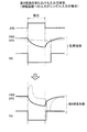
図16に第6実施形態の第1具体例による第1従来技術からの改善効果を示す。図16の上段が第1従来技術における増幅回路102Aの応答波形を示す(図30、参照)。パルス波形VM2が大振幅であるため、パルス終端でのテール特性が顕著となり、出力端子RXにおいてパルス幅が大きくなってしまう。これに対して、下段の第6実施形態の第1具体例では、増幅回路102の入力信号VM2の振幅が制限されているのでパルス終端でのテール特性は小さく、出力端子RXにおいてパスル幅の精度よく出力されることがわかる。
【0081】
図17に示す第6実施形態の第2具体例の電流パルス受信回路6Bは、DCキャンセル回路105B、大信号検出回路17Aが共に、差動入力として構成されている。この場合も、シングル入力構成の第1具体例と同様の作用、効果を奏するものである。また、電流電圧変換回路101Cの入力端子も差動構成IN、XINとして構成されている。差動入力IN、XINのうち、非入力端子側XINには、入力端子側INに接続されるフォトダイオードPDが有する負荷成分とバランスをとるため、負荷容量CLが接続されている。更に抵抗素子等を追加接続する構成とすることもできる。電流電圧変換回路101Cの回路上のバランスが改善され特性の改善を図ることができると共に、第1具体例と同様の作用、効果を奏するものである。
図18に第6実施形態の第2具体例による第2従来技術からの改善効果を示す。図16の場合と同様に、増幅回路102Bの入力信号VM2の振幅が制限され、パルス終端でのテール特性は小さく、出力端子RXにおいてパルス幅の精度よく出力されることがわかる。
【0082】
尚、第6実施形態では、大振幅検出回路17、17Aの出力電流ICTLをDCキャンセル回路105Aの電流IC制御用として使用する構成について例示したが、これに限定されることはなく、出力電流ICTLを直接電流電圧変換回路101B、101Cの入力端子INに入力する構成としても同様の動作を行わせることができる。
【0083】
これにより、IrDA通信等の光通信における強弱様々な光パルス信号に加えて、光パルスを電流パルスに変換するフォトダイオードPDの出力特性やパルス信号の微分波形におけるテール特性等の違いを吸収して、入力光パルスのパルス幅に精度良く一致した出力パルス幅を安定して出力することができる。
【0084】
図19に示す第7実施形態の温度キャンセル用バイアス回路7A、7Bは、小信号時の電流パルス受信回路の電流電圧変換回路101B、101Cにおいて、クランプトランジスタQ5(図14、あるいは図17、25を参照)の温度特性をキャンセルして、高温におけるクランプトランジスタQ5のリーク電流を低減して、広い温度範囲で一定な電流電圧変換抵抗を得るものである。図19のうち(A)の温度キャンセル用バイアス回路7Aは、図17等に例示されている、クランプトランジスタQ5のベース端子にバイアス電圧VAを印加する構成に対して、バイアス電圧VAに、トランジスタQ5の温度特性を抑制する温度特性を付与する場合の回路例を示している。また、(B)の温度キャンセル用バイアス回路7Bは、図14、図17等における電流電圧変換回路101B、101Cを構成する定電流源回路IBに、トランジスタQ5の温度特性を抑制する温度特性を付与する場合の回路例を示している。
【0085】
図19(A)の温度キャンセル用バイアス回路7Aは、トランジスタQ9とQ10とでカレントミラー回路を構成している。基準電圧VREFと、ベース及びコレクタ端子をダイオード接続したトランジスタQ9のコレクタ端子との間には、抵抗素子R17が、電源電圧+Vと、トランジスタQ10のコレクタ端子との間には、抵抗素子R18が接続されている。
抵抗素子R17とトランジスタQ9で決定される定電流((VREF−VBE)/R17)が、トランジスタQ10側にミラーされて、抵抗素子R18に流れることにより、抵抗素子R18とトランジスタQ10との間のバイアス電圧VAは、
VA=(+V)−R18×(VREF−VBE)/R17
となる。ここで、基準電圧VREFは温度に依存せずに一定であり、(R18/R17)についても同一の抵抗種で構成すれば温度特性は抑制される。このバイアス電圧VAが、図17等のクランプトランジスタQ5のベース端子に印加されるので、クランプトランジスタQ5のベース・エミッタ間の電圧が高温で大きくなるようにベース端子にバイアスされ、高温におけるリーク電流を抑制することができる。
【0086】
図19(B)の温度キャンセル用バイアス回路7Bにおいて、定電流源回路IREFは、アンプ37の正の入力端子に基準電圧VREFが入力され、出力端子がトランジスタQ11のベース端子に接続されている。更に、トランジスタQ11のエミッタ端子はアンプ37の負の入力端子にフィードバックされると共に、抵抗素子R19を介して接地電位に接続されている。また、バイアス電流IBの出力部では、抵抗素子R20とトランジスタQ12のベース端子に定電流IREFが流れている。抵抗素子R20の他端は、トランジスタQ12のコレクタ端子に接続されると共に、トランジスタQ14のベース端子に接続されている。トランジスタQ12、Q14のエミッタ端子は、それぞれ、ダイオード接続のトランジスタQ13、及び抵抗素子R21を介して接地電位に接続されている。
定電流IREFは、アンプ37の働きにより抵抗素子R19に基準電圧VREFが印加されるため、IREF=VREF/R19として出力される。ここで、R20の両端の電圧VR20は、
VR20=R20×IREF
=VREF×(R20/R19)
となり、基準電圧VREF、同一抵抗種の比(R20/R19)が共に温度に依らず一定であるため、VR20も一定値となる。VR20を用いてバイアス電流IBを導出すると、
IB=((2×VBE−VR20)−VBE)/R21
となる。ここで、前者のVBEはトランジスタQ12、Q13のVBE、後者のVBEはトランジスタQ14のVBEである。これらのトランジスタQ12、Q13、Q14に流れる電流を同一にすることは、各素子のパラメータを調整することで容易に行うことができる。従って、それぞれのVBEを等しくすることができ、
IB=(VBE−VR20)/R21
となる。小信号振幅時においては、ID=IBであるので、図14において、クランプトランジスタQ5のベース・エミッタ端子間には、
R14×IB=(VBE−VR20)×(R14/R21)
の電圧が印加される。ここで、VR20、(R14/R21)は共に温度に依らず一定である。従って、R14×IBにおける温度特性は、トランジスタQ12、Q13、Q14のVBE電圧の温度特性と同様な温度特性となる。このバイアス電圧R14×IBが、図14のクランプトランジスタQ5のベース・エミッタ端子間電圧として印加されるので、クランプトランジスタQ5のVBE電圧の温度特性と同様な温度特性でバイアスされることとなり、クランプトランジスタQ5の温度特性が抑制され、高温におけるリーク電流を抑制することができる。
【0087】
これにより、高温におけるエミッタフォロアトランジスタのリーク電流特性の悪化を防止することができ、広い温度範囲において、一定の電流電圧変換抵抗の低減効果と、出力電圧振幅のクランプレベルの低減効果を得ることができる。
【0088】
図20に示す第8実施形態の電流パルス受信回路8の回路図では、電流電圧変換回路101Bの差動出力端子VM0、VP0が、それぞれバッファ18、19を介して増幅回路102Bの差動入力端子VM2、VP2に接続されている。具体的には、バッファ18、19は差動出力端子構成であり、それぞれのバッファ18、19の正転出力端子VM1、VP1が、容量結合用の容量素子C12、C13を介して増幅回路102Bの差動入力端子VM2、VP2に接続されている。更に、バッファ18の反転出力端子は、容量素子で構成される微分回路20を介してバッファ19の入力端子に接続されている。
【0089】
第8実施形態では、増幅回路102Bへの入力信号が容量素子C12、C13を介して入力され入力電流パルスIPDを有効に伝播するように低い周波数をカットしている。この容量素子C12、C13に対して、微分回路20を構成する容量素子の容量値を小さく設定することにより、微分回路20を通過する周波数成分を入力パルスの周波数より高い成分のみとする。微分回路20には入力パルスの反転信号が入力されているので、出力には、入力パルスの振幅とは反対方向に微分されて急峻となった電圧信号が現れる。この微分された電圧信号がバッファ19、容量素子C13を介して増幅回路102Bの正転入力端子VP2に与えられることで、反転入力端子VM2への入力信号の振幅遷移方向とは反対方向に遷移するダイナミックなヒステリシスが得られる。
このときの波形を図21の下段に示す。上段の第2従来技術による波形(図33を参照)に比して、入力パルスの振幅遷移時に、入力端子VP2には反対方向に微分された急峻な波形が印加されることとなり、入力パルスの終端に精度よく追従して、増幅回路102Bの入力信号VM2、VP2が交差して精度の良いパルス出力が出力端子RXに得られることがわかる。
【0090】
第8実施形態では、第2従来技術に適用した場合を例示したが、第1従来技術に適用することも可能である。この場合の増幅回路102Aの入力信号VM2、VP2の波形を図22に示す。この場合も、図21における場合と同様に、パルス振幅の遷移時に反対方向に急峻に遷移して、ダイナミックなヒステリシスを実現することができ、精度の良いパルス出力が出力端子RXに得られることがわかる。
また、図20においては、差動信号のそれぞれにバッファ18、19を備える構成を例示したが、微分回路20への入力信号を出力するバッファ18を備えていれば、バッファ19を備えていなくても同様の効果を奏することができる。
更に、微分回路20の出力信号は、バッファ19の入力信号に重畳するように構成しているが、これに限定されることはなく、微分信号波形を重畳することができるノードであればどこでも良い。増幅回路102Bの正転入力端子VP2やその他の高インピーダンスのノード等、微分信号波形を有効に重畳することができるノードに接続しても同様の効果を奏することができる。
【0091】
図23に示す第8実施形態における具体例の電流パルス受信回路8Aでは、バッファとして、定電流源回路I11でバイアスされたエミッタフォロアトランジスタQ15で構成されるバッファ18Aと、同じく定電流源回路I12でバイアスされたエミッタフォロアトランジスタQ16で構成されるバッファ19Aとを備えている。また、微分回路として、容量素子C14と抵抗素子R22で構成される微分回路20Aを備えている。容量素子C14と抵抗素子R22とは、バッファ18AのトランジスタQ15のコレクタ端子に接続されると共に、抵抗素子R22の他端は電源電圧+Vに接続され、容量素子C14の他端はバッファ19Aの入力端子に接続されている。
【0092】
バッファ18A、19Aのうち、微分回路20Aへの接続を有するバッファ18Aに着目する。バッファ18Aを構成するエミッタフォロアトランジスタQ15の出力端子に接続されている容量素子C12の放電は定電流源回路I11により行なわれる。従って、バッファ18Aへのパルス信号の終了遷移に対してバッファ18Aの出力信号の遷移には一定の時間を要する。この遷移時間Δtは、容量素子C12からの定電流放電として容易に求めることができ、
Δt=C12×ΔVM1/I11
となる。この遷移時間Δtの間、定電流源回路I11からの定電流I11は、容量素子C12から流れるので、トランジスタQ15の電流が減少する。従って、この期間、トランジスタQ15のコレクタ端子は電圧レベルが上昇し、微分された反転信号のように振舞う。このときの電圧変化ΔVは、トランジスタQ15のエミッタ電流とコレクタ電流が等しいとすれば、
ΔV=R22×I11
となる。Δt期間におけるΔVの電圧上昇が、容量素子C14を介して他方のバッファ19Aの入力端子であるトランジスタQ16のベース端子に印加され、エミッタフォロア特性によりバッファ19Aの出力端子VP1に、更に容量素子C13を介して増幅回路102Bの正転入力端子VP2に印加されて、ダイナミックなヒステリシスを重畳することができる。
【0093】
これにより、微分信号が入力されるノードは高インピーダンスのノードであるので、微分信号は確実に重畳される。パルス遷移部のなまった電流パルスIPDが入力される場合においても、反転信号の微分波形をもってヒステリシス波形とするので、ヒステリシス効果を十分に得ることができ、パルス幅の精度よくパルス出力をすることができる。
IrDA通信等の光通信において、小振幅の光パルスが入力された場合に、フォトダイオードPDの出力特性が顕著に現れて電流パルスIPDの遷移部がなまった場合においても、精度のよいパルス幅の出力を得ることができる。
【0094】
図24に示す第9実施形態の電流パルス受信回路9の回路図は、第8実施形態の電流パルス受信回路8に対して、回路接続における対称性を改善し、回路動作上のバランスを良くした構成である。第8実施形態における微分回路20に代えて、バッファ18の反転出力端子に接続される微分回路21は増幅回路102Bの正転入力端子VP2に接続されている。更に、バッファ19の反転出力端子にも微分回路22が接続されており、増幅回路102Bの反転入力端子VM2に接続されている。
【0095】
バッファ18の正転出力端子VM1から容量素子C12を介して入力端子VM2に入力された正転入力信号に対しては、反転出力信号を反転した信号の微分波形が重畳され正転入力信号のパルス遷移部が強調される。また、バッファ19の正転出力端子VP1から容量素子C13を介して入力端子VP2に入力された反転入力信号に対しては、正転出力信号を反転した信号の微分波形が重畳され反転入力信号のパルス遷移部が強調される。増幅回路102Bの各入力信号のそれぞれにダイナミックなヒステリシスが重畳される。
更に、第9実施形態では、回路接続の対称性を実現しているので、PSRRが強化されることとなり、電源電圧の変動等の電源ノイズに対して誤動作のない回路構成を実現している。
【0096】
図25の具体例では、図23の第8実施形態の具体例に対して、バッファ19Aからバッファ18Aへの微分回路22Aを追加した構成となっている。更に、増幅回路102Bの入力端子VM2、VP2には、自動閾値調整回路(ATC)23が備えられている。第8実施形態における微分回路20Aと同様な動作を行う微分回路21A、22Aが、バッファ18A、19Aの双方に備えられ回路の対称性が改善されている。また、自動閾値調整回路(ATC)23により、増幅回路102Bの入力端子VM2、VP2における入力信号間の差を所定範囲内に維持することができ、増幅回路102Bにおける入力信号差に基づく応答特性を所定範囲内に維持することができる。
【0097】
これにより、増幅回路102Bの各入力端子VM2、VP2における回路の対称性が確保されるため、各入力端子VM2、VP2に至る信号経路における負荷、ノイズ等の外乱、電源電圧+Vの変動等は、両信号経路に同等に作用することとなるので、これらの変動に対しても安定した動作を確保することができる。
【0098】
尚、本発明は前記実施形態に限定されるものではなく、本発明の趣旨を逸脱しない範囲内で種々の改良、変形が可能であることは言うまでもない。
従って、各実施形態において説明したように、様々な改良、変形が可能であると共に、これらの改良、変形以外にも例えば、構成トランジスタをバイポーラトランジスタからMOSトランジスタへ、またはその逆に変更した構成とすることが可能である。また、差動入出力と単相入出力とのそれぞれにおいて、同様に本発明を適用することができる。
また、本実施形態においては、光パルスを受信する場合を中心に説明したが、これに限定されるものではなく、温度、圧力、加速度等の光以外の物理量を入力として、その入力を電流に変換するシステムにおいても適用が可能である。
【0099】
(付記1) 入力電流パルスを電圧パルスに変換する電流電圧変換部と、
前記電流電圧変換部からの出力信号と、該出力信号と相補な信号あるいは基準電圧とを入力信号として比較し、論理信号パルスを出力する比較回路と、
前記比較回路からの論理信号パルスに基づき、前記比較回路の入力信号に第1所定幅のヒステリシス電圧を設定する第1ヒステリシス回路と、
前記比較回路からの論理信号パルスに基づき、前記比較回路の入力信号に第2所定幅から時間経過と共に減少するヒステリシス電圧を設定する第2ヒステリシス回路とを備えることを特徴とする電流パルス受信回路。
(付記2) 前記入力電流パルスは、受光素子からの出力信号であることを特徴とする付記1に記載の電流パルス受信回路。
(付記3) 前記比較回路への入力信号は、ヒステリシス抵抗素子を介して与えられ、
前記第1ヒステリシス回路は、
前記比較回路が前記論理信号パルスを出力している間、前記ヒステリシス抵抗素子に第1所定定電流を流す第1定電流源回路を備え、
前記第2ヒステリシス回路は、
前記比較回路が前記論理信号パルスを出力している間、前記ヒステリシス抵抗素子に第2所定電流から時間経過と共に所定割合で減少する電流を流す電流源回路を備えることを特徴とする付記1又は2に記載の電流パルス受信回路。
(付記4) 前記電流源回路は、
前記第2所定電流を出力する第2定電流源回路と、
前記第2所定電流を分流し、一方を前記ヒステリシス抵抗素子に流す分流回路とを備え、
前記分流回路は、前記所定割合で前記ヒステリシス抵抗素子への分流を減ずることを特徴とする付記3に記載の電流パルス受信回路。
(付記5) 前記電流電圧変換部と前記比較回路との間に挿入され、前記電流電圧変換部からの出力信号の電圧振幅を制限して前記比較回路に出力する電圧振幅制限回路を備えることを特徴とする付記1乃至4の少なくとも何れか1項に記載の電流パルス受信回路。
(付記6) 前記電圧振幅制限回路は、
差動増幅対で構成され、前記電流電圧変換部からの出力信号と前記相補な信号、あるいは該出力信号と前記基準電圧とが入力されることを特徴とする付記5に記載の電流パルス受信回路。
(付記7) 前記比較回路への入力信号のオフセット値を設定するオフセット設定回路を備えることを特徴とする付記1乃至6の少なくとも何れか1項に記載の電流パルス受信回路。
(付記8) 前記オフセット設定回路は、前記入力信号間に設定する所定のオフセット電圧を外部より調節することができることを特徴とする付記7に記載の電流パルス受信回路。
(付記9) 前記比較回路への入力信号の供給を行なう第1バッファ回路と、
前記第1バッファ回路の入力端子へ入力信号の供給を容量結合により行なうための容量結合素子と、
前記第1バッファ回路の入力端子と所定電位との間に接続されるバイアス抵抗素子とを備えることを特徴とする付記1乃至8の少なくとも何れか1項に記載の電流パルス受信回路。
(付記10) 前記第1バッファ回路は、エミッタフォロア回路であることを特徴とする付記9に記載の電流パルス受信回路。
(付記11) 前記第1バッファ回路は、ソースフォロア回路であることを特徴とする付記9に記載の電流パルス受信回路。
(付記12) 前記容量結合素子を介して前記第1バッファ回路へ入力信号を供給する前記電圧振幅制限回路と、
前記電流電圧変換部の出力信号における高電位側出力電圧をホールドするピークホールド回路と、
前記ピークホールド回路の出力電圧に基づき、前記電圧振幅制限回路の低電位側出力電圧を所定電圧だけ上昇させる低電位レベル上昇回路とを備えることを特徴とする付記9乃至11の少なくとも何れか1項に記載の電流パルス受信回路。
(付記13) 前記容量結合素子を介して前記第1バッファ回路へ入力信号を供給する前記電圧振幅制限回路と、
前記電流電圧変換部の出力信号を積分する積分回路と、
前記積分回路の出力電圧に基づき、前記電圧振幅制限回路の低電位側出力電圧を所定電圧だけ上昇させる低電位レベル上昇回路とを備えることを特徴とする付記9乃至11の少なくとも何れか1項に記載の電流パルス受信回路。
(付記14) 前記低電位レベル上昇回路は、
前記ピークホールド回路あるいは前記積分回路の出力電圧が入力される第2バッファ回路を備えることを特徴とする付記12又は13に記載の電流パルス受信回路。
(付記15) 前記第2バッファ回路は、エミッタフォロア回路であることを特徴とする付記14に記載の電流パルス受信回路。
(付記16) 前記第2バッファ回路は、ソースフォロア回路であることを特徴とする付記14に記載の電流パルス受信回路。
(付記17) 前記容量結合素子を介して前記第1バッファ回路へ入力信号を供給する前記電圧振幅制限回路と、
前記電流電圧変換部の出力信号における高電位側出力電圧をホールドするピークホールド回路と、
前記ピークホールド回路の出力電圧に基づき、前記電流電圧変換部の電流電圧変換抵抗を調整する抵抗率自動調整回路とを備えることを特徴とする付記9乃至11の少なくとも何れか1項に記載の電流パルス受信回路。
(付記18) 前記容量結合素子を介して前記第1バッファ回路へ入力信号を供給する前記電圧振幅制限回路と、
前記電流電圧変換部の出力信号を積分する積分回路と、
前記積分回路の出力電圧に基づき、前記電流電圧変換部の電流電圧変換抵抗を調整する抵抗率自動調整回路とを備えることを特徴とする付記9乃至11の少なくとも何れか1項に記載の電流パルス受信回路。
(付記19) 前記ピークホールド回路は、
ピーク検出の応答時間に比してピークホールドの時定数が十分に長いボルテージフォロア回路を備えることを特徴とする付記12又は17に記載の電流パルス受信回路。
(付記20) 入力電流パルスを電圧パルスに変換する電流電圧変換回路と、
前記電流電圧変換回路の出力信号の電圧振幅が所定振幅以上であることを検出する大信号検出回路と、
前記大信号検出回路からの出力信号に基づき、前記電流電圧変換回路における電流電圧変換抵抗を低減すると共に、出力電圧振幅のクランプレベルを低減するクランプ回路とを備えることを特徴とする電流パルス受信回路。
(付記21) 前記入力電流パルスは、受光素子からの出力信号であることを特徴とする付記20に記載の電流パルス受信回路。
(付記22) 前記電流電圧変換回路における直流オフセット成分をキャンセルするDCキャンセル回路を備え、
前記大信号検出回路からの出力信号に基づき、前記DCキャンセル回路における直流オフセット成分のキャンセル効果を低減することを特徴とする付記20又は21に記載の電流パルス受信回路。
(付記23) 前記電流電圧変換回路は、
電流電圧変換抵抗素子を備え、
前記クランプ回路は、
バイアス回路と、
前記電流電圧変換抵抗素子と並列に接続され、前記大信号検出回路からの出力信号に基づき、前記バイアス回路により導通状態にバイアスされる、エミッタフォロアトランジスタあるいはダイオードとを備えることを特徴とする付記20乃至22の少なくとも何れか1項に記載の電流パルス受信回路。
(付記24) 前記バイアス回路は、前記エミッタフォロアトランジスタあるいは前記ダイオードの温度特性を抑制する温度特性を有することを特徴とする付記23に記載の電流パルス受信回路。
(付記25) 前記電流電圧変換回路は、差動入力構成を有し、
非入力端子に接続されるダミー負荷を備えることを特徴とする付記20乃至24の少なくとも何れか1項に記載の電流パルス受信回路。
(付記26) 前記大信号検出回路は、
前記電流電圧変換回路の出力信号の電圧振幅が所定時間の間、所定振幅以上である場合に出力信号を出力する時定数回路を備えることを特徴とする付記20乃至25の少なくとも何れか1項に記載の電流パルス受信回路。
(付記27) 入力電流パルスを電圧パルスに変換する電流電圧変換回路と、
前記電流電圧変換回路からの出力信号に基づいて増幅動作を行う差動入力構成の増幅回路と、
前記電流電圧変換回路と前記増幅回路との間に挿入される差動出力構成のバッファ回路と、
前記バッファ回路の反転出力を微分し、前記増幅回路における他方の入力信号ラインのうち、高インピーダンスのノードに供給する微分回路とを備えることを特徴とする電流パルス受信回路。
(付記28) 前記増幅回路への各入力信号を供給する一対のバッファ回路と、
前記一対のバッファ回路の反転出力うち、少なくとも一方を微分し、他方のバッファ回路の入力信号に供給する前記微分回路とを備えることを特徴とする付記27に記載の電流パルス受信回路。
(付記29) 前記一対のバッファ回路と、
前記一対のバッファ回路の各反転出力を微分する一対の微分回路とを備え、
前記一対の微分回路を対称に配置することを特徴とする付記27又は28に記載の電流パルス受信回路。
(付記30) 前記増幅回路への入力信号の供給を容量結合により行なうための容量結合素子を備え、
前記バッファ回路は、
エミッタフォロアトランジスタと、
前記エミッタフォロアトランジスタのエミッタ端子に接続され、バイアス電流を供給する定電流源回路とを備え、
前記微分回路は、
前記エミッタフォロアトランジスタのコレクタ端子と所定電位との間に接続される微分抵抗素子と、
前記コレクタ端子と前記他方の入力信号ラインとの間に接続される微分容量素子とを備えることを特徴とする付記27乃至29の少なくとも何れか1項に記載の電流パルス受信回路。
(付記31) 前記増幅回路への入力信号の供給を容量結合により行なうための容量結合素子を備え、
前記バッファ回路は、
ソースフォロアトランジスタと、
前記ソースフォロアトランジスタのソース端子に接続され、バイアス電流を供給する定電流源回路とを備え、
前記微分回路は、
前記ソースフォロアトランジスタのドレイン端子と所定電位との間に接続される微分抵抗素子と、
前記ドレイン端子と前記他方の入力信号ラインとの間に接続される微分容量素子とを備えることを特徴とする付記27乃至29の少なくとも何れか1項に記載の電流パルス受信回路。
(付記32) 前記電流電圧変換回路からの出力信号を所定電圧振幅の範囲内に制限する自動閾値調整回路、あるいは自動ゲイン調整回路を備えることを特徴とする付記20乃至31の少なくとも何れか1項に記載の電流パルス受信回路。
【0100】
【発明の効果】
本発明によれば、光通信等において受光した光パルスを受光素子により変換した電流パルスに対して、パルス振幅の大小、パルス幅の長短に関わらず、精度よく論理レベルの電圧パルスに変換して出力する電流パルス受信回路を提供することが可能となる。
【図面の簡単な説明】
【図1】 第1実施形態の電流パルス受信回路を示す回路ブロック図である。
【図2】 第1実施形態における比較回路への入力がシングル入力の場合の入出力波形である。
【図3】 第1実施形態における比較回路への入力が差動入力の場合の入出力波形である。
【図4】 第1実施形態の電流パルス受信回路の具体例を示す回路図である。
【図5】 第1実施形態の電流パルス受信回路の具体例における入出力波形である。
【図6】 第2実施形態の電流パルス受信回路を示す回路図である。
【図7】 第2実施形態の電流パルス受信回路における入出力波形である。
【図8】 第3実施形態の電流パルス受信回路を示す回路図である。
【図9】 第4実施形態の電流パルス受信回路を示す回路図である。
【図10】 第4実施形態の電流パルス受信回路における入出力波形である。
【図11】 第5実施形態の電流パルス受信回路を示す回路図である。
【図12】 第5実施形態の電流パルス受信回路における入出力波形である。
【図13】 第6実施形態の電流パルス受信回路の第1具体例を示す要部回路図である。
【図14】 電流電圧変換回路の具体例を示す回路図である。
【図15】 第6実施形態の電流パルス受信回路における大信号検出回路と電流電圧変換回路特性の関係を示す波形である。
【図16】 第6実施形態の電流パルス受信回路の第1具体例における入出力波形である。
【図17】 第6実施形態の電流パルス受信回路の第2具体例を示す回路ブロック図である。
【図18】 第6実施形態の電流パルス受信回路の第2具体例における入出力波形である。
【図19】 第7実施形態の電流パルス受信回路における電流電圧変換回路の温特キャンセル用バイアス回路を示す回路図である。
【図20】 第8実施形態の電流パルス受信回路を示す回路ブロック図である。
【図21】 第8実施形態の増幅回路への入力が差動入力の場合の入出力波形である。
【図22】 第8実施形態の増幅回路への入力がシングル入力の場合の入出力波形である。
【図23】 第8実施形態の電流パルス受信回路の具体例を示す回路図である。
【図24】 第9実施形態の電流パルス受信回路を示す回路ブロック図である。
【図25】 第9実施形態の電流パルス受信回路の具体例を示す回路図である。
【図26】 第1従来技術の光パルス受信回路を示す回路ブロック図である。
【図27】 第2従来技術の光パルス受信回路を示す回路ブロック図である。
【図28】 第1従来技術の光パルス受信回路における比較回路の入出力応答波形である。
【図29】 第2従来技術の光パルス受信回路における比較回路の入出力応答波形である。
【図30】 第1従来技術の光パルス受信回路における大光量の場合の増幅回路の入出力応答波形である。
【図31】 第1従来技術の光パルス受信回路における小光量の場合の増幅回路の入出力応答波形である。
【図32】 第2従来技術の光パルス受信回路における大光量の場合の増幅回路の入出力応答波形である。
【図33】 第2従来技術の光パルス受信回路における小光量の場合の増幅回路の入出力応答波形である。
【符号の説明】
1、1A、2、3、4、5、6B、8、8A、9、9A
電流パルス受信回路
7A、7B 温度キャンセル用バイアス回路
11 DCヒステリシス回路
12 ACヒステリシス回路
13A、13B、13C 電圧振幅制限回路
14 オフセット設定機能付バッファ回路
15 ピークホールド回路
16 自動ゲイン調整回路
17 大信号検出回路
20、20A、21,21A、22、22A
微分回路
23 自動閾値調整回路(ATC)[0001]
BACKGROUND OF THE INVENTION
The present invention relates to a current pulse receiving circuit that converts an input current pulse into a voltage pulse of a logic level with a high pulse width and outputs the voltage pulse. In particular, the light pulse received in optical communication or the like is received by a light receiving element. The present invention relates to a current pulse receiving circuit used after being converted into a current pulse.
[0002]
[Prior art]
In recent years, an infrared data communication (IrDA communication) function for connecting a space with infrared rays has been added to a mobile terminal, a personal computer, or a mobile phone. In addition, an optical fiber communication network has been established as a communication infrastructure.
[0003]
In optical communication as described above, depending on the brightness of the environment in which the device is used, so-called disturbance light from sunlight, fluorescent light, or the like is simultaneously input to a light receiving element such as a photodiode. Become. Since these disturbance lights excite the light receiving element and cause unnecessary DC current components to flow through the current pulse receiving circuit, it is necessary to remove these DC current components.
[0004]
The transmitted / received optical pulse signal is generally a burst signal, and is a signal whose pulse width and duty ratio change. On the other hand, the photodiode PD may be rounded at the rise or fall of the current output due to its characteristics, and may have a so-called tail. Furthermore, it is common to use a differentiated waveform obtained by differentiating the pulse signal from the viewpoint of removing the DC offset component, and the output signal also has a tail. Such a tail region appears more conspicuously as the signal has a wider pulse width, and the output state of the comparison circuit or amplifier circuit may invert and malfunction. As a measure to prevent this malfunction and maintain the output state correctly and output a logic pulse with high pulse width accuracy, a significant potential difference such as hysteresis voltage has been applied to the input signal to the comparison circuit or amplifier circuit. Appending is done. This measure also improves noise resistance.
[0005]
FIG. 26 shows a current
[0006]
The pulse signal converted into a voltage by the current-
[0007]
The output from the
[0008]
FIG. 27 shows a current
Similar to the current
[0009]
[Problems to be solved by the invention]
However, in addition to the wide and narrow optical pulse widths associated with burst signals in optical communications such as IrDA communications, there are differences in tail characteristics of the current output determined from the output characteristics of the photodiode PD and tail characteristics in the differential waveform of the pulse signal. In the tail region of the current output, it is difficult to stably set a sufficient hysteresis voltage width that does not cause an erroneous output from the
As a specific example, FIG. 28 shows input / output waveforms of the response of the
When a predetermined hysteresis voltage width is added to the reference voltage VTH for a single input signal as shown in FIG. 28, it can be improved if the hysteresis voltage width is set large. However, if the hysteresis voltage width is set larger than the amplitude at the time of a small input signal, the set hysteresis voltage cannot be released, and there is a possibility that the output terminal RX may be locked while being set, which is a problem.
[0010]
When the light pulse is input with a large amount of light, the output voltage amplitude is clamped in the current-
As a specific example, FIG. 30 shows a response waveform of the
[0011]
Furthermore, when the light pulse is input with a small amount of light, the output characteristics of the photodiode PD are output as they are without being subjected to the clamping operation, so that the tail waveform becomes prominent at both the start and end of the pulse. However, since the potential difference between the input signals is widened at the pulse start, there is no response delay at the pulse start at the output terminal RX. However, at the end of the pulse, the tail waveform acts in a direction that delays the crossing of the input signals, so that the end of the pulse cannot be detected accurately as in the case of the above-described large light quantity, and the pulse width of the output terminal RX is There is a problem that it becomes larger than the actual width.
As a specific example, FIG. 31 shows a response waveform of the
[0012]
In optical communication such as IrDA communication including the infrared region, the transmitted / received optical pulse signal is generally a burst signal, and is a signal whose pulse width and duty ratio change. Further, the intensity of the transmitted light varies greatly depending on the transmission distance and transmission environment of the optical pulse signal. Therefore, there is a problem that an accurate pulse width cannot be output in response to the change in the pulse width and the change in light intensity described above.
[0013]
The present invention has been made to solve the above-mentioned problems of the prior art, and converts a current pulse obtained by converting a light pulse received in optical communication or the like by a light receiving element into a voltage pulse of a logic level with a high pulse width. An object of the present invention is to provide a current pulse receiving circuit that outputs the current.
[0014]
[Means for Solving the Problems]
In order to achieve the above object, a current pulse receiving circuit according to
[0015]
In the current pulse receiving circuit according to
[0016]
Thus, the first predetermined width of the hysteresis voltage set by the first hysteresis circuit so as to have a sufficient hysteresis voltage width with respect to the maximum pulse width in the voltage pulse converted from the input current pulse, and the second hysteresis circuit By setting the second predetermined width set by (1) and the rate of decrease over time, a sufficient hysteresis voltage width can be set for voltage pulses of all pulse widths. Therefore, when applied to optical communication such as IrDA communication, in addition to the wide and narrow optical pulse widths associated with burst signals, output characteristics of photodiodes that convert optical pulses into current pulses, tail characteristics in the differential waveform of pulse signals, etc. Thus, it is possible to stably set a sufficient hysteresis voltage width in which no erroneous output occurs in the comparison circuit even in the tail region. In particular, an accurate output pulse width can be stably output in the pulse range of the longest pulse width determined according to the setting of the second predetermined width in the second hysteresis circuit and the reduction rate with time. It is suitable for use in a receiving circuit in optical communication such as IrDA communication in which the longest input optical pulse width is determined.
Also, the hysteresis voltage width has a hysteresis voltage width that is the sum of the first predetermined width and the second predetermined width immediately after the setting, and decreases with the passage of time, and finally reaches the first predetermined width. Decrease. Therefore, by setting the first predetermined width to be equal to or smaller than the amplitude of the small amplitude input signal, it is possible to avoid the possibility that the set hysteresis voltage cannot be released and the output terminal is locked while being set. Can do.
[0017]
According to a second aspect of the present invention, in the current pulse receiving circuit according to the first aspect, a voltage amplitude limiting circuit that limits the voltage amplitude of the output signal from the current-voltage converter and outputs the voltage amplitude to the comparison circuit. It is characterized by providing.
[0018]
In the current pulse receiving circuit of the second aspect, the voltage amplitude of the input signal to the comparison circuit is limited by the voltage amplitude limiting circuit.
[0019]
Thus, the voltage amplitude limiting circuit limits the voltage amplitude of the large amplitude signal from the current-voltage converter, compresses the voltage amplitude difference from the small amplitude signal, and limits the input signal range to the comparison circuit. Therefore, the hysteresis effect by the hysteresis voltage width, which is a fixed value set by the first predetermined width by the first hysteresis circuit and the second predetermined width by the second hysteresis circuit, can always be made constant. In other words, hysteresis effects can be reliably and effectively applied from small amplitude signals to large amplitude signals, and differences in tail characteristics of the input signal are absorbed, resulting in erroneous output in the comparison circuit even in the tail region. Without this, it is possible to stably output an accurate pulse width.
Further, since the input signal range to the comparison circuit is limited, an effective hysteresis effect can be given to voltage pulses having a longer pulse width for the same hysteresis characteristic setting.
[0020]
According to a third aspect of the present invention, there is provided the current pulse receiving circuit according to the first or second aspect, further comprising an offset setting circuit that sets an offset value of an input signal to the comparison circuit.
[0021]
In the current pulse receiving circuit according to the third aspect, the offset value of the input signal to the comparison circuit is set by the offset setting circuit.
[0022]
As a result, the offset value of the input signal to the comparison circuit can be set to a desired value, so an optimum offset value is set according to the pulse width, voltage amplitude, tail characteristics, noise environment, etc. of the input signal. Therefore, it is possible to stably output an accurate pulse width without malfunction.
Further, if the offset setting circuit is configured so that the offset setting can be externally adjusted, the offset value can be appropriately changed according to the use environment, and a more stable current pulse receiving circuit can be realized.
[0023]
A current pulse receiving circuit according to claim 4 is the current pulse receiving circuit according to at least one of
[0024]
In the current pulse receiving circuit according to claim 4, after the output signal of the current-voltage converter is limited in voltage amplitude by the voltage amplitude limiting circuit, it is capacitively coupled through the capacitive coupling element and input to the first buffer circuit. It is supplied as an input signal to the comparison circuit. Furthermore, the output terminal of a peak hold circuit that holds the output voltage on the high potential side or an integration circuit that integrates the output signal is connected to the current-voltage converter, and the low potential level raising circuit is connected to the voltage based on these output voltages. The output voltage on the low potential side of the amplitude limiting circuit is increased by a predetermined voltage.
[0025]
When there is no peak hold circuit, the baseline potential of the input terminal of the first buffer circuit connected to the capacitive coupling element is the average of the voltage values of the pulse signal capacitively coupled from the voltage amplitude limiting circuit, and this signal is It becomes the input signal of the comparison circuit via the first buffer circuit, and this also becomes the reference voltage. When the duty of the positive signal pulse output from the voltage amplitude limiting circuit in IrDA communication or the like is low, the input signal voltage of the comparison circuit gradually decreases during reception of the burst signal. This tendency is prominent in large-amplitude operation where the output signal from the voltage amplitude limiter circuit is limited. Therefore, receiving a burst signal from a state where the input signal of the comparison circuit is reduced due to a large-amplitude burst signal. When there is an overshoot of the input signal when returning to the no-signal state, the potential relationship is reversed with respect to the input signal on the reference voltage side of the comparator circuit that is decreasing, and an erroneous pulse is output. there is a possibility.
Therefore, the output signal of the current-voltage converter is detected by a peak hold circuit or an integration circuit. When a burst signal is input, the output voltage of the peak hold circuit or integration circuit rises, and when the voltage reaches a predetermined potential, the low potential level increase circuit sets the low potential side output voltage of the voltage amplitude limiting circuit to the predetermined voltage. Just raise.
As a result, the low voltage side output of the voltage amplitude limiter circuit has a long output period and a small voltage amplitude, whereas the high voltage side output has a short output period but the voltage amplitude remains unchanged. As a result, the decrease in voltage amplitude at the input terminal of the comparator circuit can be eliminated, and comparison is also possible when waveform waviness occurs, including overshoot that occurs when returning from large amplitude operation. The circuit will not output false pulses. Therefore, the voltage amplitude limiter circuit can reliably and effectively provide hysteresis effects from small to large amplitude signals, and absorb differences in the tail characteristics of the input signal and compare them in the tail region. In addition to being able to stably output a precise pulse width without causing erroneous output in the circuit, it is also possible to prevent the occurrence of erroneous pulses at the end of signal reception and to stabilize the accurate pulse width. Can be output.
[0026]
A current pulse receiving circuit according to
[0027]
In the current pulse receiving circuit of
[0028]
Thus, when a large-amplitude input current pulse is input, the current-voltage conversion resistance of the current-voltage conversion unit can be adjusted and lowered, so that the output signal of the current-voltage conversion unit can be a small amplitude signal. it can. Therefore, even in IrDA communication or the like where the duty of the positive pulse is low, almost no voltage drop occurs in the baseband potential of the input signal of the capacitively coupled comparison circuit. Further, since the voltage amplitude of the signal is also reduced to the amplitude level of the small amplitude signal, no swell such as overshoot occurs in the input signal of the comparison circuit even when returning to the no-signal state at the end of the burst signal. Therefore, the comparator circuit does not output a false pulse after the burst signal ends, and the hysteresis effect can be reliably and effectively applied from the small amplitude to the large amplitude of the input current pulse. In addition to absorbing differences such as these, it is possible to stably output a precise pulse width without causing erroneous output in the comparison circuit even in the tail region, and to prevent erroneous pulses from occurring at the end of the signal. Therefore, it is possible to stably output an accurate pulse width.
[0029]
According to a sixth aspect of the present invention, there is provided a current pulse receiving circuit for converting an input current pulse into a voltage pulse, a large signal detecting circuit for detecting that the voltage amplitude of the output signal is not less than a predetermined amplitude, , Electric A DC cancellation circuit for canceling the DC offset component in the current voltage conversion circuit, and reducing the DC offset component cancellation effect in the DC cancellation circuit based on the output signal from the large signal detection circuit Reduce the output voltage clamp level by reducing the current-voltage conversion resistance in the current-voltage conversion circuit It is characterized by.
[0030]
In the current pulse receiving circuit according to claim 6, when the large signal detection circuit detects that the voltage amplitude of the voltage pulse converted from the input current pulse by the current-voltage conversion circuit is equal to or larger than a predetermined amplitude. , Electric The cancellation effect of the DC cancellation circuit that cancels the DC offset component in the current-voltage conversion circuit is reduced based on the output signal from the large signal detection circuit. This reduces the current-voltage conversion resistance in the current-voltage conversion circuit and reduces the clamp level of the output amplitude .
[0031]
As a result, when it is detected that the voltage amplitude of the output signal from the current-voltage conversion circuit is a large amplitude signal greater than or equal to a predetermined amplitude, the current-voltage conversion resistance is reduced. A change in the voltage amplitude of the output voltage can be suppressed to a low level, and a voltage signal can be converted to a voltage signal with a high pulse width accuracy over a wide current amplitude range of the input current pulse having a predetermined amplitude or more. Furthermore, since the clamp level of the output voltage amplitude is reduced, the maximum voltage amplitude can be limited, and an input current pulse having a large amplitude can be converted into a voltage pulse signal with high pulse width accuracy. In addition, based on the output signal from the large signal detection circuit, the DC offset component cancellation effect of the current-voltage conversion circuit by the DC cancellation circuit can be reduced.
Since the output voltage amplitude for large-amplitude input current pulses is also limited to a small value, the tail waveform in the output voltage signal does not become a problem, and it is possible to accurately detect the end of a pulse even for large-amplitude input current pulses. The pulse width can be output with high accuracy.
In addition to various optical pulse signals in optical communication such as IrDA communication, the difference between the output characteristics of the photodiode PD that converts the optical pulses into current pulses and the tail characteristics in the differential waveform of the pulse signals can be absorbed. An output pulse width that matches the pulse width of the pulse with high accuracy can be output stably.
[0032]
According to a seventh aspect of the present invention, there is provided a current pulse receiving circuit that converts an input current pulse into a voltage pulse, and a large signal that detects that a voltage amplitude of an output signal of the current voltage conversion circuit is equal to or larger than a predetermined amplitude. A detection circuit and a gain conversion unit that converts a current-voltage conversion resistor in the current-voltage conversion circuit from a predetermined gain to a logarithmic function gain based on an output signal from the large signal detection circuit.
[0033]
In the current pulse receiving circuit according to claim 7, when the large signal detection circuit detects that the voltage amplitude of the voltage pulse converted from the input current pulse by the current-voltage conversion circuit is equal to or larger than a predetermined amplitude, the gain converter The current-voltage conversion resistor in the voltage conversion circuit is converted from a predetermined gain to a logarithmic function gain.
[0034]
Thus, as in the case of claim 6, when it is detected that the voltage amplitude of the output signal from the current-voltage conversion circuit is a large amplitude signal having a predetermined amplitude or more, a change in the current amplitude in the input current pulse is detected. A change in the voltage amplitude of the output voltage can be suppressed to a low level, and a voltage signal can be accurately converted into a voltage signal with respect to a wide current amplitude range of an input current pulse having a predetermined amplitude or more.
[0035]
The current pulse receiving circuit according to
[0036]
In the current pulse receiving circuit according to
[0037]
As a result, the bias circuit can be set so that the emitter follower transistor or the like is turned on based on the output signal from the large signal detection circuit, so that the conduction current of the emitter transistor or the like is the logarithmic characteristic of the forward junction voltage. The current-voltage conversion resistance of the current-voltage conversion circuit can be easily reduced. Further, when the emitter transistor or the like is turned on, the output resistance can be reduced, and the clamp level of the output voltage amplitude of the current-voltage conversion circuit can be easily reduced.
[0038]
The current pulse receiving circuit according to
[0039]
In the current pulse receiving circuit of the ninth aspect, the temperature characteristic of the emitter follower transistor or the diode is suppressed by the temperature characteristic of the bias circuit.
[0040]
As a result, the temperature characteristics of the emitter follower transistor and the like are suppressed by the temperature characteristics of the bias circuit, so that deterioration of the leakage current characteristics of the emitter follower transistor and the like at high temperatures can be prevented, and a constant current can be obtained over a wide temperature range. The effect of reducing the voltage conversion resistance and the effect of reducing the clamp level of the output voltage amplitude can be obtained.
[0041]
According to a tenth aspect of the present invention, there is provided a current pulse receiving circuit, a current / voltage conversion circuit for converting an input current pulse into a voltage pulse, an amplifier circuit having a differential input configuration for performing an amplification operation based on the output signal, and a current / voltage conversion. A pair of differential output configuration buffer circuits inserted between the circuit and the amplifier circuit, and the normal output terminal of each of the pair of buffer circuits is connected to the differential input terminal of the amplifier circuit via the capacitive element. In addition to the connection, one inverting output terminal of the pair of buffer circuits is connected to the other input terminal of the pair of buffer circuits through a differentiation circuit formed of a capacitor.
[0042]
The current pulse receiving circuit according to claim 10, wherein the output signal converted from the input current pulse to the voltage pulse in the current-voltage conversion circuit is passed through the pair of differential output configuration buffer circuits to the differential input configuration amplification circuit. input. Then, the inversion output of one of the pair of buffer circuits is differentiated by the differentiation circuit constituted by the capacitive element and supplied to the other input terminal of the pair of buffer circuits.
[0043]
As a result, the inverted signal of the pulse signal is differentiated, and a signal having a steep differentiated waveform at the transition portion of the pulse signal is input to the other input signal line of the amplifier circuit. Since the node to which the differential signal is input is a high impedance node, the differential signal is surely superimposed. This signal and the input pulse signal are input to the amplifier circuit, and a hysteresis effect is given to the side of emphasizing the pulse signal in the transition portion of the pulse signal.
Therefore, even when a current pulse with a distorted pulse transition is input, the differential waveform of the inverted signal is used as a hysteresis waveform, so that a sufficient hysteresis effect can be obtained and pulse output can be performed with high accuracy in pulse width. Can do.
In optical communication such as IrDA communication, when a small-amplitude optical pulse is input, even if the output characteristics of a photodiode or the like appear remarkably and the current pulse transition part disappears, an accurate pulse width output Can be obtained.
[0044]
The current pulse receiving circuit according to
[0045]
In a current pulse receiving circuit according to an eleventh aspect, the pair of buffer circuits and the pair of differentiating circuits are arranged symmetrically with respect to the amplifier circuit, and the differential waveforms are superimposed on each other.
[0046]
As a result, the symmetry of the circuit at each input terminal of the amplifier circuit is ensured, so that a load in the signal path leading to each input terminal, disturbance such as noise, fluctuations in the power supply voltage, etc. act equally on both signal paths. Therefore, a stable operation can be ensured against these fluctuations.
[0047]
DETAILED DESCRIPTION OF THE INVENTION
Hereinafter, first to ninth embodiments in which the current pulse receiving circuit of the present invention is embodied will be described in detail with reference to the drawings based on FIGS.
FIG. 1 is a circuit block diagram showing a current pulse receiving circuit of the first embodiment. FIG. 2 shows input / output waveforms when the input to the comparison circuit in the first embodiment is a single input. FIG. 3 shows input / output waveforms when the input to the comparison circuit in the first embodiment is a differential input. FIG. 4 is a circuit diagram showing a specific example of the current pulse receiving circuit of the first embodiment. FIG. 5 shows input / output waveforms in a specific example of the current pulse receiving circuit of the first embodiment. FIG. 6 is a circuit diagram showing a current pulse receiving circuit of the second embodiment. FIG. 7 shows input / output waveforms in the current pulse receiving circuit of the second embodiment. FIG. 8 is a circuit diagram showing a current pulse receiving circuit of the third embodiment. FIG. 9 is a circuit diagram showing a current pulse receiving circuit of the fourth embodiment. FIG. 10 shows input / output waveforms in the current pulse receiving circuit of the fourth embodiment. FIG. 11 is a circuit diagram showing a current pulse receiving circuit of the fifth embodiment. FIG. 12 shows input / output waveforms in the current pulse receiving circuit of the fifth embodiment. FIG. 13 is a main part circuit diagram showing a first specific example of the current pulse receiving circuit of the sixth embodiment. FIG. 14 is a circuit diagram showing a specific example of the current-voltage conversion circuit. FIG. 15 is a waveform showing the relationship between the large signal detection circuit and the current-voltage conversion circuit characteristics in the current pulse receiving circuit of the sixth embodiment. FIG. 16 shows input / output waveforms in the first specific example of the current pulse receiving circuit of the sixth embodiment. FIG. 17 is a circuit block diagram showing a second specific example of the current pulse receiving circuit of the sixth embodiment. FIG. 18 shows input / output waveforms in the second specific example of the current pulse receiving circuit of the sixth embodiment. FIG. 19 is a circuit diagram showing a temperature characteristic canceling bias circuit of the current-voltage conversion circuit in the current pulse receiving circuit of the seventh embodiment. FIG. 20 is a circuit block diagram showing a current pulse receiving circuit of the eighth embodiment. FIG. 21 shows input / output waveforms when the input to the amplifier circuit of the eighth embodiment is a differential input. FIG. 22 shows input / output waveforms when the input to the amplifier circuit of the eighth embodiment is a single input. FIG. 23 is a circuit diagram showing a specific example of the current pulse receiving circuit of the eighth embodiment. FIG. 24 is a circuit block diagram showing a current pulse receiving circuit of the ninth embodiment. FIG. 25 is a circuit diagram showing a specific example of the current pulse receiving circuit of the ninth embodiment.
[0048]
In the circuit block diagram of the current
[0049]
In the current
[0050]
2 and 3 show the effects produced by these two
[0051]
FIG. 3 shows a case where the input signal to the comparison circuit is a differential input. Also in this case, if the DC and
[0052]
FIG. 4 shows a specific circuit diagram example of the first embodiment. The output terminal of the
[0053]
The hysteresis circuit is indicated as 11 and 12 in the figure. First, the
[0054]
In the
[0055]
When the output terminal of the
[0056]
FIG. 5 shows input / output waveforms in the
[0057]
Thereby, the first predetermined width of the hysteresis voltage set by the
Also, the hysteresis voltage width has a hysteresis voltage width that is the sum of the first predetermined width and the second predetermined width immediately after the setting, and decreases with the passage of time, and finally reaches the first predetermined width. Decrease. Therefore, by setting the first predetermined width to be equal to or smaller than the amplitude of the small amplitude input signal, it is possible to avoid the possibility that the set hysteresis voltage cannot be released and the output terminal is locked while being set. Can do.
[0058]
In the specific example of FIG. 4, the configuration in which the constant current I4 is shunted with the passage of time in order to realize an alternating hysteresis voltage is shown, but it can also be realized by other methods. For example, the output current value I4 of the constant current source circuit I4 can be configured to decrease with time. This is because the resistance element that generates the constant current I4 in the constant current source circuit I4 is an active resistance element such as a MOS transistor, and the control voltage for controlling the resistance value is changed with time, or the voltage value of the voltage source itself is changed over time. It is possible to reduce it. It is also possible to insert an active resistance element such as a MOS transistor in the constant current I4 path and increase the resistance value over time by the control voltage. As another configuration example, the resistance element R4 may be an active resistance element such as a MOS transistor, and the resistance value may be decreased over time by a control voltage.
[0059]
The circuit diagram of the current
The NMOS transistor M6 forms a differential amplification pair with the NMOS transistor M7. Resistance elements R7 and R8 are load resistances of the respective transistors M6 and M7, and are biased by the constant current source circuit I7. The reference voltage VREF is applied to the gate terminal of the NMOS transistor M7 via the resistance element R6. However, in order to balance the gate terminal of the NMOS transistor M6, a capacitive element C3 is provided between the NMOS transistor M7 and the ground potential. Yes. In the second embodiment, a single output configuration from the
The output of the differential amplification pair is taken out from the connection point between the NMOS transistor M7 and the load resistor R8 by the emitter follower transistor Q3 biased by the constant current source circuit I8. Here, the transistor Q3 and the constant current source circuit I8 replace the transistor Q1 and the constant current source circuit I1 of the first embodiment, and are balanced in the circuit configuration with the transistor Q2 and the constant current source circuit I2 on the reference voltage side. It has become the composition.
[0060]
The output voltage of the voltage
VP3 = VREF−R8 × I7 / 2−VBE
It becomes. At the time of pulse input, the bias to the gate terminal of the transistor M6 increases, and as an output voltage determined by the input / output characteristics of the differential amplification pair,
VP3 (MAX) = VREF−VBE
The voltage is output with the maximum voltage. At the end of the pulse, the bias to the gate terminal of transistor M7 increases,
VP3 (MIN) = VREF−R8 × I7−VBE
Is output as a minimum voltage. That is, the output voltage amplitude of the voltage
ΔVP3 = VP3 (MAX) −VP3 (MIN)
= R8 x I7
It becomes. An output signal with a wide dynamic range output from the
[0061]
FIG. 7 shows input / output waveforms in the
[0062]
As a result, the voltage
In addition, since the input signal range to the
[0063]
The circuit diagram of the current
[0064]
The
The signal from the capacitive element C5 is input to the gate terminal of the source follower transistor M8. This gate terminal is DC-biased from the reference voltage VREF via the resistance element R9. Here, the resistance element R9 is used for DC bias and has a high-pass filter circuit configuration in combination with the capacitance element C5, and also has a function of determining the frequency of the low-frequency noise to be cut. is there.
The source terminal of the transistor M8 is connected to the cathode terminal of the Schottky diode D1, and is connected to the constant current source circuit I9 via the resistance element R11. A connection point between the resistance element R11 and the constant current source circuit I9 is an input terminal VP3 of the
[0065]
In the steady state, the transistor M8 side and the M9 side are balanced, so the corresponding terminals of both are at the same potential. Therefore, no current flows through the Schottky diode D1. Accordingly, the terminal potential of the resistance element R11, which is a connection point with the transistor M8, becomes the same potential as the reference voltage terminal VM3 of the
[0066]
In the third embodiment, the output from the
Further, if a buffer circuit similar to the transistor Q3 is connected to the load resistance R7 side of the voltage
Furthermore, the voltage
[0067]
As a result, the offset value of the input signal to the
Further, if the offset setting in the
[0068]
In the circuit diagram of the current pulse receiving circuit 4 of the fourth embodiment shown in FIG. 9, a
[0069]
The
The emitter terminal of the transistor Q4 is connected to the output terminal VCX of the voltage
[0070]
The circuit operation will be described with reference to FIG. FIG. 10 shows the input / output characteristics of the
[0071]
Therefore, by adding a
[0072]
Further, the same effect can be obtained even if an integrating circuit is used instead of the
[0073]
Here, the integration circuit can be realized by replacing the Schottky diode D2 in the
[0074]
As a result, the voltage
[0075]
The circuit diagram of the current
[0076]
In the fifth embodiment, as shown in FIG. 12, when the output voltage of the
Here, if the output signal of the
When the effect of the fourth embodiment is unnecessary, a configuration including a voltage
Further, if the automatic
In the fifth embodiment, the automatic
Further, similar to the fourth embodiment, the same effect can be obtained even if the
[0077]
As a result, even in IrDA communication or the like where the duty of the positive pulse is low, almost no voltage drop occurs in the baseband potential of the input signal of the capacitively coupled
[0078]
FIG. 6A is a circuit diagram of the main part of the current pulse receiving circuit of the first specific example of the sixth embodiment shown in FIG. 13; a current-
In the current pulse receiving circuit of the first specific example of the sixth embodiment, both the
[0079]
As shown in FIG. 14, the current-
In the first specific example of the sixth embodiment, when the input current IPD is a small signal pulse, the input current IPD is input other than the pulse signal and is generated by the DC disturbance light such as sunlight output from the photodiode PD. It is necessary to cancel (DC). In this case, the current IC is input from the DC cancel
IB = IA + IPD (DC) −IC = ID
And When the signal amplitude is small, the current ID flows through the resistance element R14 and does not flow through the clamp transistor Q5 connected in parallel. Therefore, the currents flowing through the resistance elements R14 and R15 in the current-voltage conversion unit become equal, and the output terminals VP, The VM balances and the DC offset is canceled.
The current IC at this time is detected in the DC cancel
[0080]
When the input current IPD becomes a large amplitude pulse, the output signal of the current-
ΔVBE = R14 × ΔID
When the emitter current of the transistor Q5 is larger than the current flowing through the resistance element R14,
ΔVBE = VT × LN (ΔID / IS)
It is represented by A change in the presence or absence of the input current pulse IPD appears in the potential difference ΔVBE of the clamp transistor Q5 with a logarithmic characteristic via ΔID. That is, since the current-voltage conversion resistance is in parallel with the resistance element R14 and the emitter resistance of the clamp transistor Q5 having a small resistance value, the current-voltage conversion resistance is reduced and the output voltage amplitude is limited.
FIG. 15 shows the relationship between the current ID of the current-
FIG. 16 shows the improvement effect from the first prior art according to the first specific example of the sixth embodiment. The upper part of FIG. 16 shows the response waveform of the
[0081]
In the current
FIG. 18 shows an improvement effect from the second prior art according to the second specific example of the sixth embodiment. As in the case of FIG. 16, it can be seen that the amplitude of the input signal VM2 of the
[0082]
In the sixth embodiment, the configuration in which the output current ICTL of the large
[0083]
This absorbs differences in output characteristics of photodiode PD that converts optical pulses into current pulses and tail characteristics in the differential waveform of pulse signals, in addition to various optical pulse signals in optical communication such as IrDA communication. Therefore, it is possible to stably output an output pulse width that accurately matches the pulse width of the input light pulse.
[0084]
The temperature canceling
[0085]
In the temperature
A constant current ((VREF−VBE) / R17) determined by the resistor element R17 and the transistor Q9 is mirrored on the transistor Q10 side and flows to the resistor element R18, thereby causing a bias between the resistor element R18 and the transistor Q10. The voltage VA is
VA = (+ V) −R18 × (VREF−VBE) / R17
It becomes. Here, the reference voltage VREF is constant without depending on the temperature, and the temperature characteristic is suppressed if (R18 / R17) is formed of the same resistance type. Since this bias voltage VA is applied to the base terminal of the clamp transistor Q5 shown in FIG. 17 and the like, the bias voltage is biased to the base terminal so that the voltage between the base and the emitter of the clamp transistor Q5 increases at a high temperature, and leakage current at a high temperature is reduced. Can be suppressed.
[0086]
In the temperature
The constant current IREF is output as IREF = VREF / R19 because the reference voltage VREF is applied to the resistance element R19 by the action of the
VR20 = R20 × IREF
= VREF x (R20 / R19)
Since both the reference voltage VREF and the ratio of the same resistance type (R20 / R19) are constant regardless of the temperature, VR20 also has a constant value. When the bias current IB is derived using VR20,
IB = ((2 × VBE−VR20) −VBE) / R21
It becomes. Here, the former VBE is the VBE of the transistors Q12 and Q13, and the latter VBE is the VBE of the transistor Q14. Making the currents flowing through these transistors Q12, Q13, and Q14 the same can be easily performed by adjusting the parameters of each element. Therefore, each VBE can be made equal,
IB = (VBE-VR20) / R21
It becomes. Since ID = IB at the small signal amplitude, in FIG. 14, between the base and emitter terminals of the clamp transistor Q5,
R14 × IB = (VBE−VR20) × (R14 / R21)
Is applied. Here, both VR20 and (R14 / R21) are constant regardless of the temperature. Therefore, the temperature characteristic of R14 × IB is similar to the temperature characteristic of the VBE voltage of the transistors Q12, Q13, and Q14. Since this bias voltage R14 × IB is applied as the voltage between the base and emitter terminals of the clamp transistor Q5 in FIG. 14, it is biased with a temperature characteristic similar to the temperature characteristic of the VBE voltage of the clamp transistor Q5. The temperature characteristic of Q5 is suppressed, and the leakage current at high temperature can be suppressed.
[0087]
As a result, it is possible to prevent the leakage current characteristics of the emitter follower transistor from deteriorating at high temperatures, and to obtain a constant current-voltage conversion resistance reduction effect and an output voltage amplitude clamp level reduction effect over a wide temperature range. it can.
[0088]
In the circuit diagram of the current
[0089]
In the eighth embodiment, the low frequency is cut so that the input signal to the
The waveform at this time is shown in the lower part of FIG. Compared with the waveform of the second prior art in the upper stage (see FIG. 33), a sharp waveform differentiated in the opposite direction is applied to the input terminal VP2 at the time of amplitude transition of the input pulse, and the input pulse It can be seen that the input signals VM2 and VP2 of the
[0090]
In the eighth embodiment, the case where the present invention is applied to the second conventional technique is illustrated, but the present invention can also be applied to the first conventional technique. The waveforms of the input signals VM2 and VP2 of the
In FIG. 20, the configuration including the
Further, the output signal of the differentiating
[0091]
In the current
[0092]
Of the
Δt = C12 × ΔVM1 / I11
It becomes. During this transition time Δt, the constant current I11 from the constant current source circuit I11 flows from the capacitive element C12, so that the current of the transistor Q15 decreases. Therefore, during this period, the collector terminal of the transistor Q15 rises in voltage level and behaves like a differentiated inverted signal. Assuming that the emitter current and the collector current of the transistor Q15 are equal, the voltage change ΔV at this time is
ΔV = R22 × I11
It becomes. The voltage increase of ΔV in the Δt period is applied to the base terminal of the transistor Q16, which is the input terminal of the
[0093]
Thus, since the node to which the differential signal is input is a high impedance node, the differential signal is surely superimposed. Even when a current pulse IPD having a pulse transition portion is inputted, a hysteresis waveform is obtained by using a differential waveform of the inverted signal, so that a sufficient hysteresis effect can be obtained and a pulse output can be performed with high accuracy of the pulse width. it can.
In optical communication such as IrDA communication, when a light pulse with a small amplitude is input, even when the output characteristics of the photodiode PD appear remarkably and the transition part of the current pulse IPD disappears, the pulse width with high accuracy can be obtained. Output can be obtained.
[0094]
The circuit diagram of the current
[0095]
The normal input signal input from the normal output terminal VM1 of the
Furthermore, in the ninth embodiment, since the symmetry of circuit connection is realized, PSRR is strengthened, and a circuit configuration that does not malfunction due to power supply noise such as fluctuations in power supply voltage is realized.
[0096]
In the specific example of FIG. 25, a differentiating
[0097]
Thereby, since the symmetry of the circuit at each input terminal VM2, VP2 of the
[0098]
The present invention is not limited to the above-described embodiment, and it goes without saying that various improvements and modifications can be made without departing from the spirit of the present invention.
Therefore, as described in each embodiment, various improvements and modifications are possible, and besides these improvements and modifications, for example, the configuration transistor is changed from a bipolar transistor to a MOS transistor or vice versa. Is possible. Further, the present invention can be similarly applied to each of differential input / output and single-phase input / output.
Further, in the present embodiment, the description has focused on the case of receiving an optical pulse. However, the present invention is not limited to this, and a physical quantity other than light, such as temperature, pressure, and acceleration, is used as input, and the input is used as current. The present invention can also be applied to a conversion system.
[0099]
(Supplementary note 1) a current-voltage converter that converts an input current pulse into a voltage pulse;
A comparison circuit that compares the output signal from the current-voltage converter with a signal complementary to the output signal or a reference voltage as an input signal and outputs a logic signal pulse;
A first hysteresis circuit for setting a hysteresis voltage having a first predetermined width in an input signal of the comparison circuit based on a logic signal pulse from the comparison circuit;
A current pulse receiving circuit, comprising: a second hysteresis circuit that sets a hysteresis voltage that decreases with time from a second predetermined width in an input signal of the comparison circuit based on a logic signal pulse from the comparison circuit.
(Supplementary note 2) The current pulse receiving circuit according to
(Supplementary Note 3) An input signal to the comparison circuit is given through a hysteresis resistance element,
The first hysteresis circuit includes:
A first constant current source circuit for supplying a first predetermined constant current to the hysteresis resistance element while the comparison circuit outputs the logic signal pulse;
The second hysteresis circuit includes:
Note 1 or 2 further comprising: a current source circuit for supplying a current that decreases at a predetermined rate with time from the second predetermined current to the hysteresis resistance element while the comparison circuit outputs the logic signal pulse. The current pulse receiving circuit described in 1.
(Supplementary Note 4) The current source circuit is
A second constant current source circuit for outputting the second predetermined current;
A shunt circuit for shunting the second predetermined current and passing one through the hysteresis resistance element;
The current pulse receiving circuit according to
(Supplementary Note 5) A voltage amplitude limiting circuit that is inserted between the current-voltage conversion unit and the comparison circuit and limits the voltage amplitude of the output signal from the current-voltage conversion unit and outputs the voltage amplitude to the comparison circuit. 5. The current pulse receiving circuit according to
(Supplementary Note 6) The voltage amplitude limiting circuit includes:
6. The current pulse receiving circuit according to
(Supplementary note 7) The current pulse receiving circuit according to any one of
(Supplementary note 8) The current pulse receiving circuit according to supplementary note 7, wherein the offset setting circuit can adjust a predetermined offset voltage set between the input signals from the outside.
(Supplementary note 9) a first buffer circuit for supplying an input signal to the comparison circuit;
A capacitive coupling element for performing supply of an input signal to the input terminal of the first buffer circuit by capacitive coupling;
The current pulse receiving circuit according to any one of
(Supplementary note 10) The current pulse receiving circuit according to
(Supplementary note 11) The current pulse receiving circuit according to
(Supplementary note 12) The voltage amplitude limiting circuit for supplying an input signal to the first buffer circuit via the capacitive coupling element;
A peak hold circuit for holding the high potential side output voltage in the output signal of the current-voltage converter,
And a low potential level increasing circuit for increasing the low potential side output voltage of the voltage amplitude limiting circuit by a predetermined voltage based on the output voltage of the peak hold circuit. The current pulse receiving circuit described in 1.
(Supplementary note 13) The voltage amplitude limiting circuit for supplying an input signal to the first buffer circuit via the capacitive coupling element;
An integrating circuit for integrating the output signal of the current-voltage converter,
At least one of the
(Supplementary Note 14) The low potential level raising circuit includes:
14. The current pulse receiving circuit according to
(Supplementary note 15) The current pulse receiving circuit according to
(Supplementary note 16) The current pulse receiving circuit according to
(Supplementary Note 17) The voltage amplitude limiting circuit that supplies an input signal to the first buffer circuit via the capacitive coupling element;
A peak hold circuit for holding the high potential side output voltage in the output signal of the current-voltage converter,
The current according to any one of
(Supplementary note 18) The voltage amplitude limiting circuit for supplying an input signal to the first buffer circuit via the capacitive coupling element;
An integrating circuit for integrating the output signal of the current-voltage converter,
The current pulse according to any one of
(Supplementary note 19) The peak hold circuit is
18. The current pulse receiving circuit according to
(Supplementary note 20) a current-voltage conversion circuit that converts an input current pulse into a voltage pulse;
A large signal detection circuit for detecting that the voltage amplitude of the output signal of the current-voltage conversion circuit is greater than or equal to a predetermined amplitude;
A current pulse receiving circuit comprising: a clamp circuit that reduces a current-voltage conversion resistance in the current-voltage conversion circuit and a clamp level of an output voltage amplitude based on an output signal from the large signal detection circuit .
(Supplementary note 21) The current pulse receiving circuit according to
(Supplementary Note 22) A DC cancellation circuit that cancels a DC offset component in the current-voltage conversion circuit is provided,
The current pulse receiving circuit according to
(Supplementary Note 23) The current-voltage conversion circuit includes:
It has a current-voltage conversion resistance element,
The clamp circuit is
A bias circuit;
(Supplementary note 20) An emitter follower transistor or a diode connected in parallel with the current-voltage conversion resistor element and biased to a conductive state by the bias circuit based on an output signal from the large signal detection circuit. 23. The current pulse receiving circuit according to at least one of
(Supplementary note 24) The current pulse receiving circuit according to
(Supplementary Note 25) The current-voltage conversion circuit has a differential input configuration,
25. The current pulse receiving circuit according to
(Supplementary Note 26) The large signal detection circuit includes:
At least one of the
(Supplementary note 27) a current-voltage conversion circuit for converting an input current pulse into a voltage pulse;
An amplifier circuit having a differential input configuration for performing an amplification operation based on an output signal from the current-voltage converter circuit;
A buffer circuit having a differential output configuration inserted between the current-voltage conversion circuit and the amplifier circuit;
A current pulse receiving circuit comprising: a differentiating circuit for differentiating an inverted output of the buffer circuit and supplying the differentiated output signal to a high impedance node of the other input signal line in the amplifier circuit.
(Supplementary note 28) A pair of buffer circuits for supplying each input signal to the amplifier circuit;
28. The current pulse receiving circuit according to appendix 27, further comprising: a differentiating circuit that differentiates at least one of the inverted outputs of the pair of buffer circuits and supplies the differentiated output to an input signal of the other buffer circuit.
(Supplementary note 29) the pair of buffer circuits;
A pair of differentiating circuits for differentiating each inverted output of the pair of buffer circuits,
29. The current pulse receiving circuit according to appendix 27 or 28, wherein the pair of differentiating circuits are arranged symmetrically.
(Supplementary Note 30) A capacitive coupling element for performing input signal supply to the amplifier circuit by capacitive coupling,
The buffer circuit is
An emitter follower transistor;
A constant current source circuit connected to the emitter terminal of the emitter follower transistor for supplying a bias current;
The differentiation circuit is:
A differential resistance element connected between a collector terminal of the emitter follower transistor and a predetermined potential;
30. The current pulse receiving circuit according to any one of appendices 27 to 29, further comprising: a differential capacitance element connected between the collector terminal and the other input signal line.
(Supplementary Note 31) A capacitive coupling element for performing input signal supply to the amplifier circuit by capacitive coupling,
The buffer circuit is
A source follower transistor;
A constant current source circuit connected to a source terminal of the source follower transistor and supplying a bias current;
The differentiation circuit is:
A differential resistance element connected between a drain terminal of the source follower transistor and a predetermined potential;
30. The current pulse receiving circuit according to any one of appendices 27 to 29, further comprising a differential capacitance element connected between the drain terminal and the other input signal line.
(Additional remark 32) At least any one of
[0100]
【The invention's effect】
According to the present invention, a current pulse obtained by converting a light pulse received in optical communication or the like by a light receiving element is accurately converted to a voltage pulse of a logic level regardless of the magnitude of the pulse amplitude or the length of the pulse width. It is possible to provide an output current pulse receiving circuit.
[Brief description of the drawings]
FIG. 1 is a circuit block diagram showing a current pulse receiving circuit of a first embodiment.
FIG. 2 is an input / output waveform when the input to the comparison circuit in the first embodiment is a single input.
FIG. 3 is an input / output waveform when the input to the comparison circuit in the first embodiment is a differential input.
FIG. 4 is a circuit diagram showing a specific example of the current pulse receiving circuit of the first embodiment.
FIG. 5 is an input / output waveform in a specific example of the current pulse receiving circuit of the first embodiment.
FIG. 6 is a circuit diagram showing a current pulse receiving circuit of a second embodiment.
FIG. 7 is an input / output waveform in the current pulse receiving circuit of the second embodiment.
FIG. 8 is a circuit diagram showing a current pulse receiving circuit of a third embodiment.
FIG. 9 is a circuit diagram showing a current pulse receiving circuit of a fourth embodiment.
FIG. 10 is an input / output waveform in the current pulse receiving circuit of the fourth embodiment.
FIG. 11 is a circuit diagram showing a current pulse receiving circuit of a fifth embodiment.
FIG. 12 is an input / output waveform in the current pulse receiving circuit of the fifth embodiment.
FIG. 13 is a main part circuit diagram showing a first specific example of a current pulse receiving circuit according to a sixth embodiment;
FIG. 14 is a circuit diagram showing a specific example of a current-voltage conversion circuit.
FIG. 15 is a waveform showing the relationship between the large signal detection circuit and the current-voltage conversion circuit characteristics in the current pulse receiving circuit of the sixth embodiment.
FIG. 16 shows input / output waveforms in the first specific example of the current pulse receiving circuit of the sixth embodiment.
FIG. 17 is a circuit block diagram showing a second specific example of the current pulse receiving circuit of the sixth embodiment.
FIG. 18 shows input / output waveforms in the second specific example of the current pulse receiving circuit of the sixth embodiment.
FIG. 19 is a circuit diagram showing a temperature characteristic canceling bias circuit of the current-voltage conversion circuit in the current pulse receiving circuit of the seventh embodiment.
FIG. 20 is a circuit block diagram showing a current pulse receiving circuit according to an eighth embodiment.
FIG. 21 shows input / output waveforms when the input to the amplifier circuit of the eighth embodiment is a differential input.
FIG. 22 is an input / output waveform when the input to the amplifier circuit of the eighth embodiment is a single input.
FIG. 23 is a circuit diagram showing a specific example of a current pulse receiving circuit of an eighth embodiment.
FIG. 24 is a circuit block diagram showing a current pulse receiving circuit of a ninth embodiment.
FIG. 25 is a circuit diagram showing a specific example of the current pulse receiving circuit of the ninth embodiment.
FIG. 26 is a circuit block diagram showing an optical pulse receiving circuit according to the first prior art.
FIG. 27 is a circuit block diagram showing an optical pulse receiving circuit according to a second prior art.
FIG. 28 is an input / output response waveform of the comparison circuit in the first conventional optical pulse receiving circuit.
FIG. 29 is an input / output response waveform of the comparison circuit in the optical pulse receiving circuit of the second prior art.
FIG. 30 is an input / output response waveform of the amplifier circuit in the case of a large amount of light in the optical pulse receiving circuit of the first prior art.
FIG. 31 is an input / output response waveform of an amplifier circuit in the case of a small amount of light in the first conventional optical pulse receiver circuit.
FIG. 32 is an input / output response waveform of the amplifier circuit in the case of a large amount of light in the second conventional optical pulse receiving circuit.
FIG. 33 is an input / output response waveform of the amplifier circuit in the case of a small amount of light in the second conventional optical pulse receiving circuit.
[Explanation of symbols]
1, 1A, 2, 3, 4, 5, 6B, 8, 8A, 9, 9A
Current pulse receiver circuit
7A, 7B Temperature cancellation bias circuit
11 DC hysteresis circuit
12 AC hysteresis circuit
13A, 13B, 13C Voltage amplitude limiting circuit
14 Buffer circuit with offset setting function
15 Peak hold circuit
16 Automatic gain adjustment circuit
17 Large signal detection circuit
20, 20A, 21, 21A, 22, 22A
Differentiation circuit
23 Automatic threshold adjustment circuit (ATC)
Claims (11)
前記電流電圧変換部からの出力信号と、該出力信号と相補な信号あるいは基準電圧とを入力信号として比較し、論理信号パルスを出力する比較回路と、
前記比較回路からの論理信号パルスに基づき、前記比較回路の入力信号に第1所定幅のヒステリシス電圧を設定する第1ヒステリシス回路と、
前記比較回路からの論理信号パルスに基づき、前記比較回路の入力信号に第2所定幅から時間経過と共に減少するヒステリシス電圧を設定する第2ヒステリシス回路とを備えることを特徴とする電流パルス受信回路。A current-voltage converter for converting an input current pulse into a voltage pulse;
A comparison circuit that compares the output signal from the current-voltage converter with a signal complementary to the output signal or a reference voltage as an input signal and outputs a logic signal pulse;
A first hysteresis circuit for setting a hysteresis voltage having a first predetermined width in an input signal of the comparison circuit based on a logic signal pulse from the comparison circuit;
A current pulse receiving circuit, comprising: a second hysteresis circuit that sets a hysteresis voltage that decreases with time from a second predetermined width in an input signal of the comparison circuit based on a logic signal pulse from the comparison circuit.
前記第1バッファ回路の入力端子へ入力信号の供給を容量結合により行なうための容量結合素子と、
前記第1バッファ回路の入力端子と所定電位との間に接続されるバイアス抵抗素子と、
前記容量結合素子を介して前記第1バッファ回路へ入力信号を供給する前記電圧振幅制限回路と、
前記電流電圧変換部の出力信号における高電位側出力電圧をホールドするピークホールド回路、あるいは該出力信号を積分する積分回路と、
前記ピークホールド回路、あるいは前記積分回路の出力電圧に基づき、前記電圧振幅制限回路の低電位側出力電圧を所定電圧だけ上昇させる低電位レベル上昇回路とを備えることを特徴とする請求項1乃至3の少なくとも何れか1項に記載の電流パルス受信回路。A first buffer circuit for supplying an input signal to the comparison circuit;
A capacitive coupling element for performing supply of an input signal to the input terminal of the first buffer circuit by capacitive coupling;
A bias resistor element connected between an input terminal of the first buffer circuit and a predetermined potential;
The voltage amplitude limiting circuit for supplying an input signal to the first buffer circuit via the capacitive coupling element;
A peak hold circuit for holding the high-potential side output voltage in the output signal of the current-voltage converter, or an integration circuit for integrating the output signal;
4. A low potential level increasing circuit for increasing a low potential side output voltage of the voltage amplitude limiting circuit by a predetermined voltage based on an output voltage of the peak hold circuit or the integrating circuit. The current pulse receiving circuit according to claim 1.
前記第1バッファ回路の入力端子へ入力信号の供給を容量結合により行なうための容量結合素子と、
前記第1バッファ回路の入力端子と所定電位との間に接続されるバイアス抵抗素子と、
前記容量結合素子を介して前記第1バッファ回路への入力信号を供給する前記電圧振幅制限回路と、
前記電流電圧変換部の出力信号における高電位側出力電圧をホールドするピークホールド回路、あるいは該出力信号を積分する積分回路と、
前記ピークホールド回路、あるいは前記積分回路の出力電圧に基づき、前記電流電圧変換部の電流電圧変換抵抗を調整する抵抗率自動調整回路とを備えることを特徴とする請求項1乃至3の少なくとも何れか1項に記載の電流パルス受信回路。A first buffer circuit for supplying an input signal to the comparison circuit;
A capacitive coupling element for performing supply of an input signal to the input terminal of the first buffer circuit by capacitive coupling;
A bias resistor element connected between an input terminal of the first buffer circuit and a predetermined potential;
The voltage amplitude limiting circuit for supplying an input signal to the first buffer circuit via the capacitive coupling element;
A peak hold circuit for holding the high-potential side output voltage in the output signal of the current-voltage converter, or an integration circuit for integrating the output signal;
4. A resistivity automatic adjustment circuit that adjusts a current-voltage conversion resistance of the current-voltage conversion unit based on an output voltage of the peak hold circuit or the integration circuit. 2. The current pulse receiving circuit according to item 1.
前記電流電圧変換回路の出力信号の電圧振幅が所定振幅以上であることを検出する大信号検出回路と、
前記電流電圧変換回路における直流オフセット成分をキャンセルするDCキャンセル回路とを備え、
前記大信号検出回路からの出力信号に基づき、前記DCキャンセル回路における直流オフセット成分のキャンセル効果を低減することにより前記電流電圧変換回路における電流電圧変換抵抗を低減して出力振幅のクランプレベルを低減することを特徴とする電流パルス受信回路。A current-voltage conversion circuit for converting an input current pulse into a voltage pulse;
A large signal detection circuit for detecting that the voltage amplitude of the output signal of the current-voltage conversion circuit is greater than or equal to a predetermined amplitude ;
And a DC cancel circuit for canceling a DC offset component before Symbol current-voltage conversion circuit,
Based on the output signal from the large signal detection circuit, the effect of canceling the DC offset component in the DC cancellation circuit is reduced, thereby reducing the current-voltage conversion resistance in the current-voltage conversion circuit and reducing the clamp level of the output amplitude. current pulse receiving circuit, characterized in that.
前記電流電圧変換回路の出力信号の電圧振幅が所定振幅以上であることを検出する大信号検出回路と、
前記大信号検出回路からの出力信号に基づき、前記電流電圧変換回路における電流電圧変換抵抗を、所定ゲインから対数関数ゲインに変換するゲイン変換部とを備えることを特徴とする電流パルス受信回路。A current-voltage conversion circuit for converting an input current pulse into a voltage pulse;
A large signal detection circuit for detecting that the voltage amplitude of the output signal of the current-voltage conversion circuit is greater than or equal to a predetermined amplitude;
A current pulse receiving circuit comprising: a gain conversion unit that converts a current-voltage conversion resistor in the current-voltage conversion circuit from a predetermined gain to a logarithmic function gain based on an output signal from the large signal detection circuit.
電流電圧変換抵抗素子を備え、
前記クランプ回路は、
バイアス回路と、
前記電流電圧変換抵抗素子と並列に接続され、前記大信号検出回路からの出力信号に基づき前記バイアス回路により導通状態にバイアスされる、エミッタフォロアトランジスタあるいはダイオードとを備えることを特徴とする請求項6又は7に記載の電流パルス受信回路。The current-voltage conversion circuit is
It has a current-voltage conversion resistance element,
The clamp circuit is
A bias circuit;
7. An emitter-follower transistor or a diode connected in parallel with the current-voltage conversion resistance element and biased to a conductive state by the bias circuit based on an output signal from the large signal detection circuit. Or the current pulse receiving circuit according to 7.
前記電流電圧変換回路からの出力信号に基づいて増幅動作を行う差動入力構成の増幅回路と、
前記電流電圧変換回路と前記増幅回路との間に挿入される一対の差動出力構成のバッファ回路とを備え、
前記一対のバッファ回路の各々の正転出力端子を、容量素子を介して前記増幅回路の差動入力端子に接続すると共に、
前記一対のバッファ回路のうち一方の反転出力端子を、容量素子で構成される微分回路を介して、前記一対のバッファ回路のうち他方の入力端子に接続することを特徴とする電流パルス受信回路。A current-voltage conversion circuit for converting an input current pulse into a voltage pulse;
An amplifier circuit having a differential input configuration for performing an amplification operation based on an output signal from the current-voltage converter circuit;
A buffer circuit having a pair of differential outputs inserted between the current-voltage conversion circuit and the amplifier circuit;
A normal output terminal of each of the pair of buffer circuits is connected to a differential input terminal of the amplifier circuit through a capacitive element, and
A current pulse receiving circuit, wherein one inverting output terminal of the pair of buffer circuits is connected to the other input terminal of the pair of buffer circuits via a differentiating circuit constituted by a capacitive element.
前記電流電圧変換回路からの出力信号に基づいて増幅動作を行う差動入力構成の増幅回路と、
前記電流電圧変換回路と前記増幅回路との間に挿入され、前記増幅回路への各入力信号を供給する一対の差動出力構成のバッファ回路と、
前記一対のバッファ回路の各反転出力を微分し、他方のバッファ回路の各入力端子に供給する一対の微分回路とを備えることを特徴とする電流パルス受信回路。A current-voltage conversion circuit for converting an input current pulse into a voltage pulse;
An amplifier circuit having a differential input configuration for performing an amplification operation based on an output signal from the current-voltage converter circuit;
A buffer circuit having a pair of differential outputs, which is inserted between the current-voltage conversion circuit and the amplifier circuit, and supplies each input signal to the amplifier circuit;
A current pulse receiving circuit comprising: a pair of differentiating circuits for differentiating each inverted output of the pair of buffer circuits and supplying the differentiated output to each input terminal of the other buffer circuit.
Priority Applications (4)
| Application Number | Priority Date | Filing Date | Title |
|---|---|---|---|
| JP2001021224A JP4342111B2 (en) | 2001-01-30 | 2001-01-30 | Current pulse receiver circuit |
| US09/922,764 US6456141B1 (en) | 2001-01-30 | 2001-08-07 | Current pulse receiving circuit |
| US10/214,149 US6714063B2 (en) | 2001-01-30 | 2002-08-08 | Current pulse receiving circuit |
| US10/681,306 US6891408B2 (en) | 2001-01-30 | 2003-10-09 | Current pulse receiving circuit |
Applications Claiming Priority (1)
| Application Number | Priority Date | Filing Date | Title |
|---|---|---|---|
| JP2001021224A JP4342111B2 (en) | 2001-01-30 | 2001-01-30 | Current pulse receiver circuit |
Publications (3)
| Publication Number | Publication Date |
|---|---|
| JP2002232272A JP2002232272A (en) | 2002-08-16 |
| JP2002232272A5 JP2002232272A5 (en) | 2006-10-12 |
| JP4342111B2 true JP4342111B2 (en) | 2009-10-14 |
Family
ID=18886818
Family Applications (1)
| Application Number | Title | Priority Date | Filing Date |
|---|---|---|---|
| JP2001021224A Expired - Fee Related JP4342111B2 (en) | 2001-01-30 | 2001-01-30 | Current pulse receiver circuit |
Country Status (2)
| Country | Link |
|---|---|
| US (3) | US6456141B1 (en) |
| JP (1) | JP4342111B2 (en) |
Cited By (1)
| Publication number | Priority date | Publication date | Assignee | Title |
|---|---|---|---|---|
| KR20210042004A (en) * | 2019-10-08 | 2021-04-16 | 에스케이하이닉스 주식회사 | Derivative receiver and method for receiving a signal |
Families Citing this family (47)
| Publication number | Priority date | Publication date | Assignee | Title |
|---|---|---|---|---|
| DE10328749B4 (en) * | 2003-06-25 | 2005-04-07 | Zentrum Mikroelektronik Dresden Ag | Method and arrangement for the formation of received pulses in an infrared receiver |
| US6885443B2 (en) * | 2003-07-03 | 2005-04-26 | Infineon Technologies Ag | Drive device for a light-emitting component |
| EP1501001A1 (en) * | 2003-07-22 | 2005-01-26 | STMicroelectronics Limited | Bias Circuitry |
| KR100515078B1 (en) * | 2003-09-03 | 2005-09-14 | 삼성전기주식회사 | Current-voltage transforming circuit employing limiter circuit by means of current sensing |
| JP4113824B2 (en) * | 2003-09-24 | 2008-07-09 | シリンクス株式会社 | Receiver circuit for optical space communication |
| JP3881336B2 (en) * | 2003-12-09 | 2007-02-14 | ローム株式会社 | Optical receiver and data communication apparatus including the same |
| US7536107B2 (en) * | 2004-03-31 | 2009-05-19 | Intel Corporation | Optical offset signal cancellation for optical receiver |
| JP4556481B2 (en) * | 2004-05-14 | 2010-10-06 | 住友電気工業株式会社 | Optical transceiver |
| US7394996B2 (en) | 2004-06-16 | 2008-07-01 | Industrial Technology Research Institute | Burst mode optical receiver and system and method therefor |
| JP4138708B2 (en) * | 2004-07-12 | 2008-08-27 | 浜松ホトニクス株式会社 | Photodetector |
| US7309852B2 (en) * | 2004-10-18 | 2007-12-18 | Avago Technologies Ecbu Ip (Singapore) Pte Ltd. | Variable noise control for an optical transducer |
| US7684518B2 (en) * | 2005-04-28 | 2010-03-23 | Freescale Semiconductor, Inc. | Logic threshold acquisition circuits and methods using reversed peak detectors |
| US7599631B2 (en) * | 2005-05-06 | 2009-10-06 | Yi Heqing | Burst optical receiver with AC coupling and integrator feedback network |
| JP4668690B2 (en) * | 2005-06-01 | 2011-04-13 | ルネサスエレクトロニクス株式会社 | Signal conversion circuit |
| US7570112B2 (en) * | 2005-12-15 | 2009-08-04 | Siemens Medical Solutions Usa, Inc. | Ultrasound imaging or other use variable input impedance preamplifier |
| US7368991B2 (en) * | 2006-01-05 | 2008-05-06 | Texas Instruments Incorporated | System and method for clamping a differential amplifier |
| US7358819B2 (en) * | 2006-01-17 | 2008-04-15 | Rockwell Automation Technologies, Inc. | Reduced-size sensor circuit |
| US7622981B2 (en) * | 2006-12-06 | 2009-11-24 | Linear Technology Corporation | Square cell having wide dynamic range and power detector implementing same |
| TWI339375B (en) * | 2007-01-29 | 2011-03-21 | Chimei Innolux Corp | Liquid crystal display device and driving method using the same |
| US7414234B1 (en) * | 2007-02-02 | 2008-08-19 | Alcatel Lucent | Measurement of burst mode optical power over multiple bursts |
| US8564978B2 (en) * | 2007-03-22 | 2013-10-22 | Thomson Licensing | Apparatus for supplying isolated regulated DC power to electronics devices |
| TWI462496B (en) * | 2007-10-03 | 2014-11-21 | Airoha Tech Corp | The biasing circuit of the wireless transceiver |
| JP5176505B2 (en) * | 2007-12-03 | 2013-04-03 | 富士通オプティカルコンポーネンツ株式会社 | Optical receiving device, optical station side device, and optical network system |
| US8129671B2 (en) * | 2007-12-11 | 2012-03-06 | Renesas Electronics Corporation | Power supply dependent optical receiver and amplifier and photocoupler using the same |
| JP5108559B2 (en) * | 2008-02-28 | 2012-12-26 | ルネサスエレクトロニクス株式会社 | Buffer circuit and light receiving circuit using the same |
| JP5147457B2 (en) * | 2008-02-29 | 2013-02-20 | ザインエレクトロニクス株式会社 | Input buffer circuit |
| US8150273B2 (en) * | 2008-09-04 | 2012-04-03 | Finisar Corporation | Optical receiver with threshold voltage compensation |
| JP2012235376A (en) * | 2011-05-06 | 2012-11-29 | Sumitomo Electric Ind Ltd | Electronic circuit and light-receiving circuit |
| JP2012090284A (en) * | 2011-11-14 | 2012-05-10 | Fujitsu Optical Components Ltd | Optical receiving device, optical station side apparatus and optical network system |
| JP5762943B2 (en) * | 2011-12-27 | 2015-08-12 | 株式会社東芝 | Optical transceiver circuit and receiving circuit |
| CN107395162B (en) * | 2012-03-15 | 2020-05-01 | 飞兆半导体公司 | Clamping circuit and method for clamping voltage |
| US9753559B2 (en) * | 2012-10-19 | 2017-09-05 | Texas Instruments Incorporated | Feedback integrator current source, transistor, and resistor coupled to input |
| US8901955B2 (en) | 2012-11-05 | 2014-12-02 | Sandisk Technologies Inc. | High speed buffer with high noise immunity |
| US8803550B2 (en) | 2012-12-12 | 2014-08-12 | Sandisk Technologies Inc. | Dynamic high speed buffer with wide input noise margin |
| JP6217258B2 (en) * | 2013-09-06 | 2017-10-25 | ソニー株式会社 | Current-voltage conversion circuit, optical receiver, and optical transmission system |
| JP6217294B2 (en) * | 2013-10-07 | 2017-10-25 | ソニー株式会社 | Optical receiver circuit, optical receiver, and optical transmission system |
| CN104467386A (en) * | 2014-11-19 | 2015-03-25 | 成都创图科技有限公司 | High-stability low-pass filter inverter system |
| US9923642B2 (en) * | 2015-02-23 | 2018-03-20 | Mitsubishi Electric Corporation | Light receiving device |
| US10568530B2 (en) | 2015-06-27 | 2020-02-25 | Intel Corporation | Apparatus and method for tracking and cancelling DC offset to acquire small AC signal |
| US10541652B2 (en) | 2015-06-27 | 2020-01-21 | Intel Corporation | Apparatus and method for filter settling calibration to improve speed of tracking and cancelling of DC offset |
| US10231632B2 (en) | 2016-02-22 | 2019-03-19 | Intel Corporation | Apparatus and method for tracking and cancelling DC offset to acquire small AC signal using dual feedback loops |
| CN107171723A (en) * | 2016-03-08 | 2017-09-15 | 深圳光启智能光子技术有限公司 | Light, which is made an uproar, removes circuit and optical receiver |
| CN107425877B (en) * | 2017-06-23 | 2019-07-30 | 江苏本能科技有限公司 | Radio-frequency carrier offsets method and system |
| US10498461B1 (en) * | 2018-09-19 | 2019-12-03 | Elenion Technologies, Llc | Optical receivers with dc cancellation bias circuit and embedded offset cancellation |
| CN113711491A (en) * | 2019-06-13 | 2021-11-26 | 住友电气工业株式会社 | Optical receiver, station-side device, PON system, preamplifier, optical receiving method, and method for suppressing output inversion of integrator |
| CN115314104B (en) * | 2022-08-09 | 2024-03-12 | 无锡飞龙九霄微电子有限公司 | Low-noise RSSI circuit and working method thereof |
| CN117118409B (en) * | 2023-10-24 | 2024-01-09 | 上海兴感半导体有限公司 | Hysteresis comparison circuit and electronic chip |
Family Cites Families (11)
| Publication number | Priority date | Publication date | Assignee | Title |
|---|---|---|---|---|
| US4292469A (en) * | 1979-06-13 | 1981-09-29 | Scott Instruments Company | Voice pitch detector and display |
| FR2555839B1 (en) * | 1983-11-25 | 1986-01-24 | Thomson Csf | BROADBAND AMPLIFIER-LIMITER DEVICE |
| US5057683A (en) * | 1988-10-28 | 1991-10-15 | Astex Co., Ltd. | Error preventive circuit for a photoelectric switch |
| JP2756820B2 (en) * | 1989-03-31 | 1998-05-25 | 三菱電機株式会社 | Semiconductor laser drive circuit |
| US5381106A (en) * | 1992-10-28 | 1995-01-10 | Samsung Electronics Co., Ltd. | Clipper circuitry suitable for signals with fractional-volt amplitudes |
| KR950003637B1 (en) * | 1992-12-03 | 1995-04-17 | 삼성전자 주식회사 | Frequency modulation system |
| JPH08315054A (en) * | 1995-05-23 | 1996-11-29 | Advantest Corp | Analog division circuit |
| JPH10290127A (en) * | 1997-04-17 | 1998-10-27 | Rohm Co Ltd | Current/voltage conversion ic and photoelectric conversion ic |
| US6091287A (en) * | 1998-01-23 | 2000-07-18 | Motorola, Inc. | Voltage regulator with automatic accelerated aging circuit |
| US6188294B1 (en) * | 1999-05-12 | 2001-02-13 | Parthus Technologies, Plc. | Method and apparatus for random sequence generator |
| US6300752B1 (en) * | 1999-05-24 | 2001-10-09 | Level One Communications, Inc. | Common mode bias voltage generator |
-
2001
- 2001-01-30 JP JP2001021224A patent/JP4342111B2/en not_active Expired - Fee Related
- 2001-08-07 US US09/922,764 patent/US6456141B1/en not_active Expired - Lifetime
-
2002
- 2002-08-08 US US10/214,149 patent/US6714063B2/en not_active Expired - Lifetime
-
2003
- 2003-10-09 US US10/681,306 patent/US6891408B2/en not_active Expired - Lifetime
Cited By (1)
| Publication number | Priority date | Publication date | Assignee | Title |
|---|---|---|---|---|
| KR20210042004A (en) * | 2019-10-08 | 2021-04-16 | 에스케이하이닉스 주식회사 | Derivative receiver and method for receiving a signal |
Also Published As
| Publication number | Publication date |
|---|---|
| US20040075484A1 (en) | 2004-04-22 |
| US6456141B1 (en) | 2002-09-24 |
| US6891408B2 (en) | 2005-05-10 |
| US20020101270A1 (en) | 2002-08-01 |
| US6714063B2 (en) | 2004-03-30 |
| US20020190777A1 (en) | 2002-12-19 |
| JP2002232272A (en) | 2002-08-16 |
Similar Documents
| Publication | Publication Date | Title |
|---|---|---|
| JP4342111B2 (en) | Current pulse receiver circuit | |
| US5329115A (en) | Optical receiver circuit | |
| US4498001A (en) | Transimpedance amplifier for optical receivers | |
| US7567105B2 (en) | High speed controller area network receiver having improved EMI immunity | |
| JP2651031B2 (en) | Digital data receiver | |
| US8841972B2 (en) | Electronic device, fiber-optic communication system comprising the electronic device and method of operating the electronic device | |
| JP5658287B2 (en) | Optical signal detection circuit and optical receiver | |
| US5844445A (en) | Feedback type pre-amplifier | |
| US20030197563A1 (en) | Amplification circuit and optical communication apparatus provided with the amplification circuit | |
| US11394349B2 (en) | Transimpedance amplifier | |
| US20080284522A1 (en) | Linear transimpedance amplifier with multiplexed gain stage | |
| JPH0563056B2 (en) | ||
| JPH098563A (en) | Light receiving preamplifier | |
| US9882539B1 (en) | Multi-data rate, burst-mode transimpedance amplifier (TIA) circuit | |
| US6879217B2 (en) | Triode region MOSFET current source to bias a transimpedance amplifier | |
| TWI279096B (en) | Optical receiver | |
| JP4248773B2 (en) | Current-voltage converter | |
| US6798282B1 (en) | Method and system for transimpedance amplifiers with high current input while maintaining high transimpedance gain and bandwidth | |
| CN114614908B (en) | Optical receiver and transimpedance amplifier chip thereof | |
| KR20160073902A (en) | Audio switch circuit with slow turn-on | |
| US6897731B2 (en) | Method and circuit for overload recovery of an amplifier | |
| WO2022263047A1 (en) | Transimpedance amplifier circuit | |
| JP3927336B2 (en) | Preamplifier circuit | |
| JP2020010203A (en) | Transimpedance amplifier circuit | |
| JP5096507B2 (en) | Amplitude limiting amplifier circuit and optical receiver |
Legal Events
| Date | Code | Title | Description |
|---|---|---|---|
| A711 | Notification of change in applicant |
Free format text: JAPANESE INTERMEDIATE CODE: A711 Effective date: 20050830 |
|
| A521 | Request for written amendment filed |
Free format text: JAPANESE INTERMEDIATE CODE: A523 Effective date: 20060825 |
|
| A621 | Written request for application examination |
Free format text: JAPANESE INTERMEDIATE CODE: A621 Effective date: 20060825 |
|
| A711 | Notification of change in applicant |
Free format text: JAPANESE INTERMEDIATE CODE: A712 Effective date: 20080728 |
|
| A977 | Report on retrieval |
Free format text: JAPANESE INTERMEDIATE CODE: A971007 Effective date: 20081022 |
|
| A131 | Notification of reasons for refusal |
Free format text: JAPANESE INTERMEDIATE CODE: A131 Effective date: 20081209 |
|
| A521 | Request for written amendment filed |
Free format text: JAPANESE INTERMEDIATE CODE: A523 Effective date: 20090123 |
|
| TRDD | Decision of grant or rejection written | ||
| A01 | Written decision to grant a patent or to grant a registration (utility model) |
Free format text: JAPANESE INTERMEDIATE CODE: A01 Effective date: 20090707 |
|
| A01 | Written decision to grant a patent or to grant a registration (utility model) |
Free format text: JAPANESE INTERMEDIATE CODE: A01 |
|
| A61 | First payment of annual fees (during grant procedure) |
Free format text: JAPANESE INTERMEDIATE CODE: A61 Effective date: 20090707 |
|
| FPAY | Renewal fee payment (event date is renewal date of database) |
Free format text: PAYMENT UNTIL: 20120717 Year of fee payment: 3 |
|
| R150 | Certificate of patent or registration of utility model |
Ref document number: 4342111 Country of ref document: JP Free format text: JAPANESE INTERMEDIATE CODE: R150 Free format text: JAPANESE INTERMEDIATE CODE: R150 |
|
| FPAY | Renewal fee payment (event date is renewal date of database) |
Free format text: PAYMENT UNTIL: 20120717 Year of fee payment: 3 |
|
| S531 | Written request for registration of change of domicile |
Free format text: JAPANESE INTERMEDIATE CODE: R313531 |
|
| S533 | Written request for registration of change of name |
Free format text: JAPANESE INTERMEDIATE CODE: R313533 |
|
| FPAY | Renewal fee payment (event date is renewal date of database) |
Free format text: PAYMENT UNTIL: 20120717 Year of fee payment: 3 |
|
| R371 | Transfer withdrawn |
Free format text: JAPANESE INTERMEDIATE CODE: R371 |
|
| S531 | Written request for registration of change of domicile |
Free format text: JAPANESE INTERMEDIATE CODE: R313531 |
|
| S533 | Written request for registration of change of name |
Free format text: JAPANESE INTERMEDIATE CODE: R313533 |
|
| FPAY | Renewal fee payment (event date is renewal date of database) |
Free format text: PAYMENT UNTIL: 20120717 Year of fee payment: 3 |
|
| R350 | Written notification of registration of transfer |
Free format text: JAPANESE INTERMEDIATE CODE: R350 |
|
| FPAY | Renewal fee payment (event date is renewal date of database) |
Free format text: PAYMENT UNTIL: 20120717 Year of fee payment: 3 |
|
| FPAY | Renewal fee payment (event date is renewal date of database) |
Free format text: PAYMENT UNTIL: 20130717 Year of fee payment: 4 |
|
| S111 | Request for change of ownership or part of ownership |
Free format text: JAPANESE INTERMEDIATE CODE: R313113 |
|
| R350 | Written notification of registration of transfer |
Free format text: JAPANESE INTERMEDIATE CODE: R350 |
|
| R250 | Receipt of annual fees |
Free format text: JAPANESE INTERMEDIATE CODE: R250 |
|
| R250 | Receipt of annual fees |
Free format text: JAPANESE INTERMEDIATE CODE: R250 |
|
| S111 | Request for change of ownership or part of ownership |
Free format text: JAPANESE INTERMEDIATE CODE: R313111 |
|
| R350 | Written notification of registration of transfer |
Free format text: JAPANESE INTERMEDIATE CODE: R350 |
|
| R250 | Receipt of annual fees |
Free format text: JAPANESE INTERMEDIATE CODE: R250 |
|
| R250 | Receipt of annual fees |
Free format text: JAPANESE INTERMEDIATE CODE: R250 |
|
| R250 | Receipt of annual fees |
Free format text: JAPANESE INTERMEDIATE CODE: R250 |
|
| LAPS | Cancellation because of no payment of annual fees |