JP4337186B2 - Image information conversion apparatus, image information conversion method, learning apparatus, and learning method - Google Patents
Image information conversion apparatus, image information conversion method, learning apparatus, and learning method Download PDFInfo
- Publication number
- JP4337186B2 JP4337186B2 JP30948499A JP30948499A JP4337186B2 JP 4337186 B2 JP4337186 B2 JP 4337186B2 JP 30948499 A JP30948499 A JP 30948499A JP 30948499 A JP30948499 A JP 30948499A JP 4337186 B2 JP4337186 B2 JP 4337186B2
- Authority
- JP
- Japan
- Prior art keywords
- value
- output
- statistical data
- pixel
- image signal
- Prior art date
- Legal status (The legal status is an assumption and is not a legal conclusion. Google has not performed a legal analysis and makes no representation as to the accuracy of the status listed.)
- Expired - Fee Related
Links
- 238000000034 method Methods 0.000 title claims description 31
- 238000006243 chemical reaction Methods 0.000 title claims description 14
- 238000000605 extraction Methods 0.000 claims description 45
- 230000015556 catabolic process Effects 0.000 claims description 14
- 238000006731 degradation reaction Methods 0.000 claims description 14
- 230000007274 generation of a signal involved in cell-cell signaling Effects 0.000 claims description 11
- 230000000593 degrading effect Effects 0.000 claims description 4
- 238000013500 data storage Methods 0.000 claims description 3
- 230000006866 deterioration Effects 0.000 claims description 3
- 238000004364 calculation method Methods 0.000 description 16
- 230000003044 adaptive effect Effects 0.000 description 10
- 238000010586 diagram Methods 0.000 description 10
- 230000015654 memory Effects 0.000 description 9
- 230000006978 adaptation Effects 0.000 description 7
- 239000000284 extract Substances 0.000 description 5
- 230000005540 biological transmission Effects 0.000 description 2
- 230000011218 segmentation Effects 0.000 description 2
- 230000000694 effects Effects 0.000 description 1
- 239000011159 matrix material Substances 0.000 description 1
- 238000012986 modification Methods 0.000 description 1
- 230000004048 modification Effects 0.000 description 1
- 230000002123 temporal effect Effects 0.000 description 1
Images

Landscapes
- Editing Of Facsimile Originals (AREA)
- Facsimile Image Signal Circuits (AREA)
- Image Processing (AREA)
- Picture Signal Circuits (AREA)
Description
【0001】
【発明の属する技術分野】
この発明は、入力画像信号のぼけを改善するための画像情報変換装置および画像情報変換方法、学習装置および学習方法に関する。
【0002】
【従来の技術】
近年、クラス分類適応処理を用いてぼけを改善することにより、画質改善を行う処理が研究開発されている。クラス分類適応処理は、入力画像信号の信号レベル分布に応じてクラス分類を行い、クラス毎に予め学習によって獲得された予測係数値を所定の記憶部に格納し、かかる予測係数値を使用した重み付け加算式によって注目画素の画素値として最適な推定値を出力する処理である。
【0003】
この場合、注目画素についてのクラス分類を行う際に必要なデータを得るために当該注目画素の周辺に配置されるクラスタップや、当該注目画素の画素値を推定する演算を行う際に必要なデータを得るために当該注目画素の周辺に配置される予測タップを、適応的に、すなわち注目画素毎に最適な間引き間隔で配置することができれば、そのような間引き間隔についての制御を行わない場合に比べ、大幅な画質改善が可能となる。しかしながら、そのような制御は実現されていなかった。
【0004】
【発明が解決しようとする課題】
従って、この発明の目的は、クラス分類適応処理を用いて画質改善を行う際に、画質改善の程度を向上させることが可能な、画像情報変換装置および画像情報変換方法、学習装置および学習方法を提供することにある。
【0005】
【課題を解決するための手段】
請求項1の発明は、入力画像信号を、相異なる複数種類の間引き間隔で間引いた画像から、夫々予測画素値を生成する予測画像信号生成手段と、
予測画像信号生成手段から出力される複数の予測画素値の内の最大値および最小値の一方を、入力画像信号の特徴に基づいて選択的に出力する最適画素値出力手段とを備え、
最適画素値出力手段は、
入力画像信号から、注目画素の周辺に指定される所定位置の画素値を統計的データ用クラスタップとして出力する統計的データ用クラスタップ抽出手段と、
統計的データ用クラスタップ抽出手段の出力に基づいて、統計的データ用クラスコードを発生する統計的データ用クラスコード発生手段と、
統計的データを予め記憶し、統計的データ用クラスコード発生手段の出力に対応する統計的データを出力する統計的データ記憶手段と、
統計的データ記憶手段の出力に基づいて、最大値および最小値の内から、最適な値を出力する出力値決定手段とを備えることを特徴とする画像情報変換装置である。
【0006】
請求項4の発明は、入力画像信号を、相異なる複数種類の間引き間隔で間引いた画像から、夫々予測画素値を生成する予測画像信号生成ステップと、
予測画像信号生成ステップによって生成される複数の予測画素値の内の最大値および最小値の一方を、入力画像信号の特徴に基づいて選択的に出力する最適画素値出力ステップとを備え、
最適画素値出力ステップは、
入力画像信号から、注目画素の周辺に指定される所定位置の画素値を統計的データ用クラスタップとして出力する統計的データ用クラスタップ抽出ステップと、
統計的データ用クラスタップ抽出ステップの出力に基づいて、統計的データ用クラスコードを発生する統計的データ用クラスコード発生ステップと、
予め記憶されている統計的データから、統計的データ用クラスコード発生ステップにより発生される統計的データ用クラスコードに対応する統計的データを出力する統計的データ出力ステップと、
統計的データ出力ステップの出力に基づいて、最大値および最小値の内から、最適な値を出力する出力値決定ステップとを備えることを特徴とする画像情報変換方法である。
【0007】
請求項5の発明は、入力画像信号を劣化させる信号劣化処理手段と、
信号劣化処理手段から出力される画像を相異なる複数種類の間引き間隔で間引いた画像から、夫々予測画素値を生成する予測画像信号生成手段と、
入力画像信号を参照して、予測画像信号生成手段から出力される複数の予測画素値の内の最大値および最小値の一方を選択的に出力する最適画素値出力手段と、
最適画素値出力手段の出力の内、所定の条件を満たすものの個数を、当該画素が最大値、最小値の内の何れであったかの区分、および信号劣化処理手段から出力される画像の特徴を表現する情報を発生する手段の出力に対応して計数する計数手段とを備えることを特徴とする学習装置である。
【0008】
請求項11の発明は、入力画像信号を劣化させる信号劣化処理ステップと、
信号劣化処理ステップによって生成される画像を相異なる複数種類の間引き間隔で間引いた画像から、夫々予測画素値を生成する予測画像信号生成ステップと、
入力画像信号を参照して、予測画像信号生成ステップによって生成される複数の予測画素値の内の最大値および最小値の一方を選択的に出力する最適画素値出力ステップと、
最適画素値出力ステップの結果の内、所定の条件を満たすものの個数を、当該画素が最大値、最小値の内の何れであったかの区分、および信号劣化処理ステップによって生成される画像の特徴を表現する情報を発生するステップの出力に対応して計数するステップとを備えることを特徴とする学習方法である。
【0009】
以上のような発明によれば、互いに異なる間引き間隔を有する複数種類のクラスタップ構造に基づくクラス分類適応処理の結果の内で最適なものが出力画像信号として選択される。
【0010】
【発明の実施の形態】
以下、この発明の一実施形態について説明する。なお、クラス分類適応処理は、入力画像信号の信号レベル分布等の入力画像信号の特徴データに応じてクラス分類を行い、クラス毎に予め学習によって獲得された予測係数値を所定の記憶部に格納し、かかる予測係数値を使用した重み付け加算式によって注目画素の画素値として最適な推定値を出力する処理である。
【0011】
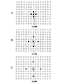
入力画像信号の信号レベル分布を把握してクラス分類を行うために、入力画像信号上にクラスタップが配置される。クラスタップは、入力画像信号の信号レベル分布を表現する特徴を計算するためのデータとして、入力画像信号の所定位置から抽出される画素値である。クラスタップは、例えば、注目画素を含むフレーム上と、その前後のフレーム上とに配置される。注目画素を含むフレーム上におけるクラスタップ構造の一例を図1に示す。ここで、図1Aは、間引き間隔1すなわち注目画素に対して縦/横に隣接する、画素位置にクラスタップが配置される。すなわち、間引き間隔1の場合、間引きがなされないことになる。また、図1Bは、間引き間隔2すなわち注目画素に対して縦/横に2番目の画素位置にクラスタップが配置される。さらに、図1Cは、間引き間隔3すなわち注目画素に対して縦/横に3番目の画素位置にクラスタップが配置される。同様に、間引き間隔4、5等、間引き間隔をさらに広げたクラスタップ配置を用いることもできる。ぼけ画像においては、ぼけの範囲の広がりの程度に応じて、何れの間引き間隔の下でクラス分類を行うのが最適であるかが異なる。
【0012】
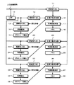
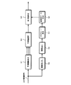
以下、この発明の一実施形態についての説明に先立って、複数種類の間引き量の下で設定されたクラスタップ配置において、クラス分類適応処理によるぼけ画像の画質改善を行うための、既に提案されている構成について説明する。まず、学習、すなわち予測係数を得るための処理に係る構成の一例を図2に示す。ぼけを含まない、所定の入力画像信号(教師信号と称される)がLPF(Low Pass Filter) 回路10と、領域切り出し回路11とに供給される。LPF回路10は、入力画像信号にLPF処理を施して、劣化した(ぼけの生じた)画像信号を生成し、劣化した画像信号を領域切り出し回路12、13および領域切り出し回路22、23、並びに領域切り出し回路32、33に供給する。
【0013】
領域切り出し回路12は、劣化した画像信号から所定範囲の画素領域を予測タップとして切り出し、切り出した領域を正規方程式加算回路16に供給する。また、領域切り出し回路13は、図1Aに示したような間引き間隔1のクラスタップ配置の下で所定範囲の画素領域をクラスタップとして切り出し、切り出した領域を特徴抽出回路14に供給する。特徴抽出回路14は、領域切り出し回路13の出力に基づいて劣化した画像信号の特徴を抽出し、抽出した特徴をクラスコード発生回路15に供給する。クラスコード発生回路15は、特徴抽出回路14の出力に基づいてクラスコードを発生させ、発生させたクラスコードを正規方程式加算回路16に供給する。
【0014】
一方、領域切り出し回路11は、教師信号から所定の画素領域を切り出し、切り出した領域を正規方程式加算回路16に供給する。正規方程式加算回路16は、領域切り出し回路11の出力、領域切り出し回路12の出力、およびクラスコード発生回路15の出力に基づいて所定の計算処理を行って、クラス毎に予測係数を算出するための正規方程式に係るデータを生成し、生成したデータを予測係数決定回路17に供給する。予測係数決定回路17は、供給されるデータに基づいて正規方程式を解く計算処理を行って予測係数を算出し、算出した予測係数をメモリ18に供給する。メモリ18は、供給される予測係数を記憶する。
【0015】
領域切り出し回路23、特徴抽出回路24、クラスコード発生回路25,正規方程式加算回路26、予測係数決定回路27、およびメモリ28は、それぞれ、上述した、領域切り出し回路13、特徴抽出回路14、クラスコード発生回路15、正規方程式加算回路16、予測係数決定回路17、およびメモリ18と同様なものである。但し、領域切り出し回路23は、図1Bに示したような間引き間隔2のクラスタップ配置の下で領域切り出しを行う。
【0016】
また、領域切り出し回路33、特徴抽出回路34、クラスコード発生回路35,正規方程式加算回路36、予測係数決定回路37、およびメモリ38は、それぞれ、上述した、領域切り出し回路13、特徴抽出回路14、クラスコード発生回路15、正規方程式加算回路16、予測係数決定回路17、およびメモリ18と同様なものである。但し、領域切り出し回路33は、図1Cに示したような間引き間隔3のクラスタップ配置の下で領域切り出しを行う。
【0017】
ここで、予測係数の算出に係る演算についてより詳細に説明する。図4を参照して後述するように、クラス分類適応処理による予測画像信号は、入力画像信号の所定の画素位置から抽出される予測タップと、学習によって得られた予測係数とに基づいて、以下の式(1)に従って順次予測生成される画素値yからなる。
【0018】
y=w1 ×x1 +w2 ×x2 +‥‥+wn ×xn (1)
ここで、x1 ,‥‥,xn が各予測タップであり、w1 ,‥‥,wn が各予測係数である。
【0019】
正規方程式加算回路16、26、36は、それぞれ、領域切り出し回路12、22、23から供給される予測タップ、およびクラスコード発生回路15、25、35から供給されるクラスコード、並びに教師信号に基づいて加算処理を行うことにより、予測係数w1 ,‥‥,wn を解とする正規方程式を解くために必要なデータを算出する。そして、予測係数決定回路17、27、37は、供給されるデータに基づいて正規方程式を解くための計算処理を行って予測係数を算出する。
【0020】
正規方程式について説明する。上述の式(1)において、学習前は予測係数w1 ,‥‥,wn が未定係数である。学習は、クラス毎に複数の教師信号を入力することによって行う。教師信号の種類数をmと表記する場合、式(1)から、以下の式(2)が設定される。
【0021】
yk =w1 ×xk1+w2 ×xk2+‥‥+wn ×xkn (2)
(k=1,2,‥‥,m)
m>nの場合、予測係数w1 ,‥‥,wn は一意に決まらないので、誤差ベクトルeの要素ek を以下の式(3)で定義して、式(4)によって定義される誤差ベクトルeを最小とするように予測係数を定めるようにする。すなわち、いわゆる最小2乗法によって予測係数を一意に定める。
【0022】
ek =yk −{w1 ×xk1+w2 ×xk2+‥‥+wn ×xkn} (3)
(k=1,2,‥‥m)
【0023】
【数1】

式(4)のe2 を最小とする予測係数を求めるための実際的な計算方法としては、e2 を予測係数wi (i=1,2‥‥)で偏微分し(式(5))、iの各値について偏微分値が0となるように各予測係数wi を定めれば良い。
【0025】
【数2】
式(5)から各予測係数wi を定める具体的な手順について説明する。式(6)、(7)のようにXji,Yi を定義すると、式(5)は、式(8)の行列式の形に書くことができる。
【0027】
【数3】
【数4】
【数5】
式(8)が一般に正規方程式と呼ばれるものである。予測係数決定回路17、27、37は、正規方程式データに基づいて、掃き出し法等の一般的な行列解法に従って正規方程式を解くための計算処理を行って予測係数wi を算出する。
【0031】
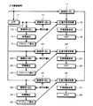
なお、図2には、予測タップの間引き間隔を固定してクラスタップの間引き間隔を変える構成を示したが、予測タップの間引き間隔を、クラスタップの間引き間隔と共に変える構成としても良い。そのような構成について図3に示す。図3において、各構成要素は、図2中で同一の符号を付したものと同様なものである。但し、領域切り出し回路12、22、32は、それぞれ、間引き間隔1、2、3のタップ構造を有する予測タップを切り出す。
【0032】
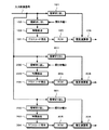
次に、この発明の一実施形態において、上述したようにして得られた予測係数を使用して、各間引き間隔の下で配置されるクラスタップ毎の予測画像信号を生成するための構成について説明する。そのような構成の一例を図4に示す。入力画像信号が領域切り出し回路101、102、201、202、301、302に供給される。ここで、入力画像信号には、伝送路等において帯域制限によってぼけが生じていることがあり、そのままでは表示画像がぼけたものとなる場合がある。領域切り出し回路101、201、301は、入力画像信号から予測タップとして使用される画素領域を切り出し、切り出した領域を、推定演算部106、206、306にそれぞれ供給する。
【0033】
一方、領域切り出し回路102、202、302は、供給される画像信号から所定の画素領域をクラスタップとして切り出し、切り出した領域を、特徴抽出回路103、203、303にそれぞれ供給する。特徴抽出回路103、203、303は、それぞれ、領域切り出し回路102、202、302の出力に基づいてぼけ画像の特徴を抽出し、抽出した特徴をクラスコード発生回路104、204、304にそれぞれ供給する。
【0034】
クラスコード発生回路104、204、304は、それぞれ、特徴抽出回路103、203、303の出力に基づいてクラスコードを発生させ、発生させたクラスコードを、ROM105、205、305にそれぞれ供給する。ROM105、205、305は、図2等を参照して上述したようにして算出された予測係数を記憶している。すなわち、図2または図3中のメモリ18、28、38の記憶内容がROM105、205、305にそれぞれ予めロードされている。
【0035】
ROM105、205、305は、それぞれ、クラスコード発生回路104、204、304の出力に対応する予測係数を出力する。出力される予測係数は、それぞれ、推定演算部106、206、306に供給される。推定演算部106、は、ROM105から供給される予測係数と、領域切り出し回路101から供給される予測タップとして使用される画素値との線型一次結合(式(1)参照)を計算することにより、各画素値yを推定し、推定される画素値yの総体としての予測画像信号を生成する。
【0036】
このようにして生成される予測画像においては、伝送路等における入力画像信号の劣化に起因する画像のぼけが解消若しくは軽減されている。なお、図4に示した構成では、領域切り出し回路101、201、301における間引き間隔は一定とされているが、図3に示した構成に対応して、領域切り出し回路101、201、301がそれぞれ、間引き間隔1、2、3のタップ構造を有する予測タップを切り出すようにしても良い。
【0037】
この発明は、クラス分類適応処理処理において上述したような例えば3種類等の複数個の間引き間隔のクラスタップ構造を用いることによって得られる例えば3種類等の複数個の予測値の内で最適な予測値を決定し、決定結果に基づいて最終的な出力画像信号を作成するようにしたものである。
【0038】
この発明の一実施形態における画像処理装置の一例を図5に示す。入力画像信号は、予測画像生成部51に供給される。予測画像生成部51は間引き間隔毎の予測画像を生成する構成であり、予測画像生成部51としては、図4を参照して上述した構成等を使用することができる。かかる構成を使用する場合には、予測画像生成部51は、例えば3種類の間引き間隔に対応する3個の予測画像信号を生成し、これら3個の予測画像信号を予測値選択回路53に供給する。但し、間引き間隔の種類、およびそれらに対応して生成される予測画像信号の個数は、3に限定されるものでは無い。予測値選択回路53は、供給される予測値の内から各画素位置毎に最大の予測値および最小の予測値を選択し、選択した予測値を出力値決定回路54に供給する。
【0039】
入力画像信号が領域切り出し回路55に供給される。領域切り出し回路55は、入力画像信号から所定の画素領域をクラスタップとして切り出し、切り出した画素領域を特徴抽出回路56に供給する。特徴抽出回路56は、領域切り出し回路55の出力に基づいてぼけ画像の特徴を抽出し、抽出した特徴をクラスコード発生回路57に供給する。クラスコード発生回路57は、特徴抽出回路56の出力に基づいてクラスコードを発生させ、発生させたクラスコードを統計的データROM58に供給する。
【0040】
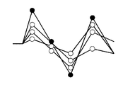
統計的データROM58は、後述するような統計的データをクラスコード毎に記憶しており、クラスコード発生回路57から供給されるクラスコードに対応する統計的データを予測値決定回路54に供給する。予測値決定回路54は、供給される統計的データを参照して、予測値選択回路53から供給される各画素位置毎の最大の予測値および最小の予測値の内で最適なものを決定し、決定結果に基づいて出力画像信号を作成する。この際の処理について図6を参照して具体的に説明する。ここで、原画像の信号波形の一例を黒丸で示す。また、この一例に対応する位置における、予測画像生成部51によって生成される予測画像信号の信号波形の一例を3個の白丸で示す。最適な予測値としては、黒丸に最も近い白丸が選択されれば良い。このためには、信号波形のピークが上に凸の場合に3個の予測値の内の最大値を選択し、信号波形のピークが下に凸の場合に3個の予測値の内の最小値を選択するようにすれば良い。また、ピーク以外の部分では、原画像信号と予測画像信号との間のレベル差が小さいので、最適な予測値としては、3個の予測値の内の何れを選んでも良い。以上の状況を考慮して、この発明の一実施形態では、予測画像生成部51によって生成される3個の予測値の内から最大および最小の予測値を予測値選択回路53が選択し、最大および最小の予測値の内から、後述するような統計的データを参照して、予測値決定回路54が出力画像信号として最適なものを選択するようになされている。
【0041】
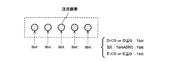
また、特徴抽出回路56が出力する、クラス分類のための特徴としては、例えば、一次微分の符号と大きさ、二次微分の符号を用いることができる。例えば、注目画素を中心とした水平5タップからなる、図7に示すようなクラスタップ構造の一例を用いる場合に、各々の画素位置について、一次微分Dの符号(すなわちDの正負)についての1ビット、一次微分Dの大きさに関する1ビット、(すなわち|D|の値を1ビットADRCで量子化した量子化値)、二次微分Eの符号(すなわちEの正負)に関する1ビットの計3ビットを割り当てる。従って、5画素に対するビット数は3×5=15ビットとなり、総クラス数は215=32768クラスとなる。ここで使用される水平5タップについて間引きを行うようにしても良い。一次微分D,二次微分Eはそれぞれ、以下の式(9)、式(10)によって計算される。
【0042】
この発明の一実施形態において、ADRC回路3は、領域切り出し回路2によって分離されたそれぞれ5画素のSDデータを各2ビットに圧縮するものとする。以下、圧縮されたSDデータをそれぞれq1 〜q5 と表記する。これらのパターン圧縮データがクラスコード発生回路6に供給される。
【0043】
D(i,j)=f(i,+j)−f(i,j−1) (9)
E(i,j)
=f(i,j+1)+f(i,j−1)−2×f(i,j) (10)
ここで、i,jは、画素位置を2次元的に表す座標であり、f(i,j)は、画素位置における画素値である。ここでは、クラスタップを2次元に配置する場合を例として説明したが、この発明は、クラスタップが3次元(時空間)内でに配置される場合等にも、適用することができる。なお、1ビットADRC(Adaptive Dynamic Range Coding)は、何らかのデータの時間的または空間的な変化パターンを少ないビット数で表現するための処理である。|D|のダイナミックレンジをDR,ビット割当をn,各画素位置における|D|のデータレベルをL,再量子化コードをQとして、以下の式(11)により、|D|の最大値maxと最小値minとの間を指定されたビット長で均等に分割して再量子化を行う。
【0044】
DR=MAX−MIN+1
Q={(L−MIN+0.5)×2/DR} (11)
但し、{ }は切り捨て処理を意味する。
【0045】
また、予測値決定回路54が2種類の統計的データを参照して動作する構成とすれば、最適な予測値をより高精度に決定することができる。このような構成の一例を図8に示す。図8中で、図5中の各構成要素と同様な構成要素には同一の符号を付した。かかる構成の一例は、統計的データの出力に係る処理系列として、領域切り出し回路55、特徴抽出回路56、クラスコード発生回路57,および統計的データROM58を含む第1の処理系列と、領域切り出し回路155、特徴抽出回路156、クラスコード発生回路157,および統計的データROM158を含む第2の処理系列とを備える。
【0046】
ここで、第1の系列が行う処理によって統計的データROM58から出力される第1の統計的データを参照して予測値決定回路54が動作した結果として曖昧な判定が行われる場合には、第2の系列が行う処理によって統計的データROM158から出力される第2の統計的データを参照して予測値決定回路54が動作するように制御する等の制御方法により、最適な予測値を決定する精度を向上させることができる。なお、クラスコードを発生させる構成を3系列以上備え、これらが発生する3種類以上のクラスコードの各々に対応して統計的データを記憶している統計的データROMも3個以上備えることにより、予測値決定回路54が3種類以上の統計的データを参照して動作するようにし、最適な予測値を決定する精度をさらに向上させることも可能である。
【0047】
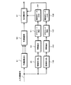
次に、予測値決定回路54の動作において参照される統計的データの生成について図9を参照して説明する。教師信号としての入力画像信号がLPF61、最適予測値選択回路64、および残差計算回路65とに供給される。LPF61は、供給される画像信号にLPF処理を施し、劣化した画像信号を生成する。LPF61の出力は、予測画像生成部62および領域切り出し回路66に供給される。
【0048】
予測画像生成部62は間引き間隔毎の予測画像を生成する構成であり、予測画像生成部62としては、図5、図8中の予測画素生成部51と同様の構成を有するものが使用される。予測画像生成部62の出力である、例えば3個の予測画像信号が第1の予測値選択回路63に供給される。予測値選択回路63は、予測画像生成部62から供給される予測値の内から各画素位置毎に最大の予測値MAXおよび最大の予測値MINを選択し、最適予測値出力回路64に供給する。
【0049】
最適予測値出力回路64は、予測値選択回路63の出力の内から教師信号との残差すなわち信号レベル差の絶対値が小さいものを選択し、選択した予測値(すなわちMAX或いはMIN)を最適な予測値として残差計算回路65に供給する。また、最適予測値出力回路64は、選択した予測値がMAX、MINの何れであるかを示す信号dカウント回路69に供給する。残差計算回路65は、最適予測値選択回路64から供給される最適な予測値と、教師信号とに基づいて残差を計算し、計算値をカウント回路69に供給する。
【0050】
一方、領域切り出し回路66は、LPF61の出力から所定の画素領域をクラスタップとして切り出し、切り出した画素領域を特徴抽出回路67に供給する。特徴抽出回路67は、領域切り出し回路66の出力に基づいて、図5中の特徴抽出回路56と同様な動作を行うことにより、画像の特徴を抽出する。特徴抽出回路67によって抽出される特徴がクラスコード発生回路68に供給される。クラスコード発生回路68は、特徴抽出回路67の出力に基づいてクラスコードを発生させ、発生させたクラスコードをカウント回路69に供給する。領域切り出し回路66、特徴抽出回路67、およびクラスコード発生回路68は、それぞれ、図5中の領域切り出し回路55、特徴抽出回路56、およびクラスコード発生回路57と同様なものとされる。
【0051】
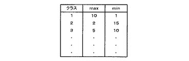
カウント回路69は、残差計算回路65から供給される残差が所定のしきい値より大きい画素のみを、クラスコード発生回路68から供給されるクラスコード、および上述の信号dによって伝えられる、当該画素が最大値/最小値の何れとして最適予測値選択回路64にて選択されたものであるかに情報に応じてカウントすることにより、統計的データを生成する。生成される統計的データは、メモリ70に供給され、記憶される。ここで、ある画素がカウントの対象とされるか否かは、例えば、当該画素に係る残差が所定のしきい値よりも大きくなるか否かに応じて判定することができる。統計的データの一例を図10に示す。図10では、クラスコードがクラス1を示す場合において、最適予測値選択回路64によって最大値が選択された場合の画素であって、当該画素と教師信号との残差がしきい値よりも大きいもののカウント数が10であり、最適予測値出力回路64によって最大値が選択された場合の画素であって、当該画素と教師信号との残差の絶対値がしきい値より大きいもののカウント数が1であることが示されている。
【0052】
また、クラスコードがクラス2を示す場合に、最大値/最小値として選択された画素であって、当該画素と教師信号との残差が大きいもののカウント数が2/15であることが示されている。同様に、クラスコードがクラス3を示す場合に、最大値/最小値として選択された画素であって、当該画素と教師信号との残差が大きいもののカウント数が5/10であることが示されている。
【0053】
このように、残差による制限、すなわち残差がある程度以上大きい画素のみをカウントすることで統計的データを得るようにすることにより、間引き間隔等の条件との関連で画質の向上に寄与する度合いが小さい部分を排除し、画質の向上に寄与する度合いが大きい部分のみが統計的データに反映するようになされる。
【0054】
また、最適予測値と教師信号との画素毎の残差以外の量に注目して、統計データに反映する部分を制限するようにしても良い。例えば、間引き間隔毎の複数の予測値の間における、ダイナミックレンジDR、または微分値の大きさを注目して、統計データに反映する部分を制限するようにした構成も可能である。この際にどのような制限を課すかによって、複数種類の統計的データを得ることができる。このようにして、図8等を参照して上述した構成において用いられる複数種類の統計的データを生成することが可能となる。また、領域切り出し回路55、と領域切り出し回路155、および特徴抽出回路56と特徴抽出回路156における処理を変えても良い。
【0055】
メモリ70に記憶された統計的データは、図5、図8中の統計的データROM58にロードされる。図5および図8中の予測値決定回路54は、予測値選択回路53から供給される最大の画素値および最小の画素値の内で、統計的データ中でカウント値が多い方を好適な予測画素値として決定するようになされる。但し、統計的データ中で最大の画素値および最小の画素値に対するカウント値が互いに拮抗している場合には、当該統計的データを参照して好適な予測画素値を決定すると、決定結果の信頼性が低いと考えられる。このような場合に決定結果が誤った場合には、大幅な画質劣化が生じるおそれがある。
【0056】
そこで、統計的データ中で最大の画素値および最小の画素値に対するカウント値が互いに拮抗している場合に以下のような処理を行うようにすることにより、予測値決定回路54が行う好適な予測画素値の決定についての信頼性を担保することができる。▲1▼図8に示したような構成において、当該統計的データ以外の統計的データを予測値決定回路54の動作において参照する。▲2▼最大の画素値と最小の画素値との平均値を予測値決定回路54から出力させる。ここで、▲1▼、▲2▼は何れも例であり、これらに限定されるものでは無い。
【0057】
なお、統計的データ中で最大の画素値および最小の画素値に対するカウント値が互いに拮抗している場合は、例えば以下の式(12)が成り立つ場合として判定することができる。
【0058】
a/(a−b)<threshould (12)
ここで、aは多い方の度数を表し、bは少ない方の度数を表す。また、threshouldは、所定のしきい値である。
【0059】
この発明は、上述したこの発明の一実施形態に限定されるものでは無く、この発明の主旨を逸脱しない範囲内で様々な変形や応用が可能である。
【0060】
【発明の効果】
上述したように、この発明は、互いに異なる間引き間隔を有する複数種類のクラスタップ構造および/または予測タップ構造に基づくクラス分類適応処理の結果の内から、統計的データを参照して最適なものを選択し、選択した画像信号を出力画像信号とするものである。
【0061】
このため、入力画像信号内の各画素位置について、当該画素位置における画像劣化の度合い、画像中の特徴等に対してより適合性の高い間引き間隔の下でのクラス分類適応処理結果を使用して、出力画像信号を生成することができる。
【0062】
特に、この発明では、画素毎に最適な間引き間隔を選択できるので、画像信号全体に対して一定の間引き間隔の下でクラス分類適応処理を行う場合に比して、より大きな画質改善を実現することができる。
【0063】
また、互いに異なる間引き間隔の下でのクラス分類適応処理の結果の内から、最大値、最小値を検出し、検出した最大値、最小値の内から最適なものを選択する処理を行うことにより、互いに異なる間引き間隔の下でのクラス分類適応処理の結果の全部(例えば3個の予測画像信号)から最適なものを選択する場合に比べ、特に信号波形のピーク付近において、容易に、且つ正確に最適な予測画像信号を選択することができる。
【0064】
さらに、統計的データを求める処理において、画像信号の特徴に関連する所定の条件が加味されるようにすることにより、画質改善のためにより的確な統計的データを得ることができる。
【0065】
また、統計的データを複数種類使用する構成とすれば、より大きな画質改善を実現することができる。
【図面の簡単な説明】
【図1】各間引き間隔におけるクラスタップ構造の一例を示す略線図である。
【図2】クラス分類適応処理における学習に係る構成の一例を示すブロック図である。
【図3】クラス分類適応処理における学習に係る構成の他の例を示すブロック図である。
【図4】クラス分類適応処理における予測推定に係る構成の一例を示すブロック図である。
【図5】この発明の一実施形態における、予測推定に係る構成の一例を示すブロック図である。
【図6】原画像信号の信号波形と、予測画像信号の信号波形との一例を示す略線図である。
【図7】統計的データを参照する際のクラス分類の一例について説明するための略線図である。
【図8】この発明の一実施形態における構成の他の例を示すブロック図である。
【図9】この発明の一実施形態における、統計的データを得るための構成の一例を示すブロック図である。
【図10】統計的データの一例を示す略線図である。
【符号の説明】
51・・・予測画像出力部、53・・・予測値選択回路、54・・・出力値決定回路、58・・・統計的データROM[0001]
BACKGROUND OF THE INVENTION
The present invention relates to an image information conversion device, an image information conversion method, a learning device, and a learning method for improving blurring of an input image signal.
[0002]
[Prior art]
In recent years, processing for improving image quality by improving blur using class classification adaptive processing has been researched and developed. The class classification adaptive process performs class classification according to the signal level distribution of the input image signal, stores the prediction coefficient value obtained by learning in advance for each class in a predetermined storage unit, and weights using the prediction coefficient value This is a process of outputting an optimum estimated value as the pixel value of the target pixel by the addition formula.
[0003]
In this case, in order to obtain data necessary for classifying the target pixel, data necessary for class taps arranged around the target pixel and calculation for estimating the pixel value of the target pixel If the prediction taps arranged around the pixel of interest are adaptively arranged, i.e., at the optimum thinning interval for each pixel of interest, control is not performed on such a thinning interval. Compared to this, the image quality can be greatly improved. However, such control has not been realized.
[0004]
[Problems to be solved by the invention]
Accordingly, an object of the present invention is to provide an image information conversion device, an image information conversion method, a learning device, and a learning method capable of improving the degree of image quality improvement when performing image quality improvement using class classification adaptation processing. It is to provide.
[0005]
[Means for Solving the Problems]
The invention according to
Optimal pixel value output means for selectively outputting one of a maximum value and a minimum value of a plurality of prediction pixel values output from the prediction image signal generation means based on the characteristics of the input image signal.,
The optimum pixel value output means is
Statistical data class tap extraction means for outputting pixel values at predetermined positions specified around the pixel of interest from the input image signal as statistical data class taps;
A statistical data class code generating means for generating a statistical data class code based on the output of the statistical data class tap extracting means;
Statistical data storage means for storing statistical data in advance and outputting statistical data corresponding to the output of the statistical data class code generating means;
Output value determining means for outputting an optimum value from the maximum value and the minimum value based on the output of the statistical data storage means;This is an image information conversion device.
[0006]
Claim4According to the invention, a predicted image signal generation step for generating a predicted pixel value from an image obtained by thinning an input image signal at a plurality of different thinning intervals;
One of the maximum value and the minimum value among the plurality of prediction pixel values generated by the prediction image signal generation step is selectively output based on the characteristics of the input image signal.Optimal pixel value outputWith steps,
The optimal pixel value output step is
A statistical data class tap extraction step for outputting a pixel value at a predetermined position specified around the pixel of interest from the input image signal as a statistical data class tap;
A class code generation step for statistical data that generates a class code for statistical data based on the output of the class tap extraction step for statistical data;
A statistical data output step of outputting statistical data corresponding to the statistical data class code generated by the statistical data class code generation step from the statistical data stored in advance;
Based on the output of the statistical data output step, an output value determination step for outputting an optimum value from the maximum value and the minimum value is provided.This is an image information conversion method characterized by the above.
[0007]
Claim5According to the present invention, signal degradation processing means for degrading an input image signal,
Predicted image signal generating means for generating predicted pixel values, respectively, from images obtained by thinning images output from the signal degradation processing means at different thinning intervals;
An optimum pixel value output means for selectively outputting one of a maximum value and a minimum value among a plurality of prediction pixel values output from the prediction image signal generation means with reference to the input image signal;
Represents the number of pixels that satisfy a predetermined condition among the outputs of the optimum pixel value output means, classifies whether the pixel is the maximum value or the minimum value, and the characteristics of the image output from the signal degradation processing means And a counting means for counting corresponding to the output of the means for generating information.
[0008]
Claim11The invention includes a signal degradation processing step for degrading an input image signal,
A predicted image signal generating step for generating predicted pixel values, respectively, from images obtained by thinning out images generated by the signal degradation processing step at different types of thinning intervals;
An optimum pixel value output step for selectively outputting one of a maximum value and a minimum value among a plurality of prediction pixel values generated by the prediction image signal generation step with reference to the input image signal;
Expresses the number of pixels that satisfy a predetermined condition among the results of the optimal pixel value output step, classifies whether the pixel is the maximum value or the minimum value, and the characteristics of the image generated by the signal degradation processing step And a step of counting corresponding to the output of the step of generating the information to be performed.
[0009]
According to the invention as described above, the optimum one among the results of the class classification adaptive processing based on a plurality of types of class tap structures having different thinning intervals is selected as the output image signal.
[0010]
DETAILED DESCRIPTION OF THE INVENTION
Hereinafter, an embodiment of the present invention will be described. The class classification adaptive process performs class classification according to the feature data of the input image signal such as the signal level distribution of the input image signal, and stores the prediction coefficient value obtained by learning in advance for each class in a predetermined storage unit. In this process, the optimum estimated value is output as the pixel value of the target pixel by the weighted addition formula using the prediction coefficient value.
[0011]
Class taps are arranged on the input image signal in order to grasp the signal level distribution of the input image signal and perform classification. The class tap is a pixel value extracted from a predetermined position of the input image signal as data for calculating a feature expressing the signal level distribution of the input image signal. For example, the class tap is arranged on the frame including the pixel of interest and on the frames before and after it. An example of the class tap structure on the frame including the target pixel is shown in FIG. Here, in FIG. 1A, class taps are arranged at pixel positions adjacent to the
[0012]
Prior to the description of an embodiment of the present invention, a class tap arrangement set under a plurality of types of thinning amounts has already been proposed for improving the image quality of blurred images by class classification adaptive processing. The configuration will be described. First, FIG. 2 shows an example of a configuration related to learning, that is, processing for obtaining a prediction coefficient. A predetermined input image signal (referred to as a teacher signal) that does not include blur is supplied to an LPF (Low Pass Filter)
[0013]
The
[0014]
On the other hand, the
[0015]
The
[0016]
In addition, the
[0017]
Here, the calculation related to the calculation of the prediction coefficient will be described in more detail. As will be described later with reference to FIG. 4, the predicted image signal by the class classification adaptive processing is based on a prediction tap extracted from a predetermined pixel position of the input image signal and a prediction coefficient obtained by learning. The pixel value y is sequentially predicted and generated according to the equation (1).
[0018]
y = w1X1+ W2X2+ ... + wnXn (1)
Where x1, ..., xnIs each prediction tap, w1, ..., wnAre each prediction coefficient.
[0019]
The normal
[0020]
The normal equation will be described. In the above equation (1), before learning, the prediction coefficient w1, ..., wnIs an undetermined coefficient. Learning is performed by inputting a plurality of teacher signals for each class. When the number of types of teacher signals is expressed as m, the following equation (2) is set from equation (1).
[0021]
yk= W1Xk1+ W2Xk2+ ... + wnXkn (2)
(K = 1, 2,..., M)
If m> n, prediction coefficient w1, ..., wnIs not uniquely determined, the element e of the error vector ekIs defined by the following equation (3), and the prediction coefficient is determined so as to minimize the error vector e defined by equation (4). That is, the prediction coefficient is uniquely determined by a so-called least square method.
[0022]
ek= Yk-{W1Xk1+ W2Xk2+ ... + wnXkn} (3)
(K = 1, 2, ... m)
[0023]
[Expression 1]
E in equation (4)2As a practical calculation method for obtaining the prediction coefficient that minimizes2Prediction coefficient wi(i = 1, 2...) is partially differentiated (formula (5)), and each prediction coefficient w is set so that the partial differential value becomes 0 for each value of i.iShould be determined.
[0025]
[Expression 2]
From equation (5), each prediction coefficient wiA specific procedure for determining the above will be described. X as in equations (6) and (7)ji, Yi(5) can be written in the form of the determinant of equation (8).
[0027]
[Equation 3]
[Expression 4]
[Equation 5]
Equation (8) is generally called a normal equation. The prediction
[0031]
FIG. 2 shows a configuration in which the prediction tap thinning interval is fixed and the class tap thinning interval is changed, but the prediction tap thinning interval may be changed together with the class tap thinning interval. Such a configuration is shown in FIG. In FIG. 3, each component is the same as that shown in FIG. However, the
[0032]
Next, in one embodiment of the present invention, a configuration for generating a predicted image signal for each class tap arranged under each thinning interval using the prediction coefficient obtained as described above will be described. To do. An example of such a configuration is shown in FIG. An input image signal is supplied to the
[0033]
On the other hand, the
[0034]
The class
[0035]
The
[0036]
In the predicted image generated in this way, blurring of an image due to deterioration of an input image signal in a transmission path or the like is eliminated or reduced. In the configuration illustrated in FIG. 4, the thinning intervals in the
[0037]
The present invention provides an optimum prediction among a plurality of prediction values such as three types obtained by using a class tap structure with a plurality of thinning intervals such as three types as described above in the class classification adaptive processing. A value is determined, and a final output image signal is created based on the determination result.
[0038]
An example of an image processing apparatus according to an embodiment of the present invention is shown in FIG. The input image signal is supplied to the predicted
[0039]
The input image signal is supplied to the
[0040]
The
[0041]
In addition, as features for classification, which are output from the
[0042]
In one embodiment of the present invention, it is assumed that the
[0043]
D (i, j) = f (i, + j) −f (i, j−1) (9)
E (i, j)
= F (i, j + 1) + f (i, j-1) -2 * f (i, j) (10)
Here, i and j are coordinates representing the pixel position two-dimensionally, and f (i, j) is a pixel value at the pixel position. Here, the case where the class taps are arranged in two dimensions has been described as an example, but the present invention can also be applied to the case where the class taps are arranged in three dimensions (time-space). Note that 1-bit ADRC (Adaptive Dynamic Range Coding) is a process for expressing a temporal or spatial change pattern of some data with a small number of bits. When the dynamic range of | D | is DR, the bit allocation is n, the data level of | D | at each pixel position is L, and the requantization code is Q, the maximum value | D | And the minimum value min are equally divided by a designated bit length to perform requantization.
[0044]
DR = MAX-
Q = {(L−MIN + 0.5) × 2 / DR} (11)
However, {} means a truncation process.
[0045]
If the predicted
[0046]
Here, when an ambiguous determination is made as a result of the operation of the predicted
[0047]
Next, generation of statistical data referred to in the operation of the predicted
[0048]
The predicted
[0049]
The optimum predicted value output circuit 64 selects the output from the predicted
[0050]
On the other hand, the
[0051]
The
[0052]
In addition, when the class code indicates
[0053]
In this way, the degree of contribution to the improvement of image quality in relation to conditions such as thinning intervals by obtaining statistical data by limiting only residual pixels, that is, counting only pixels whose residual is larger than a certain level. Are excluded, and only the part that contributes to the improvement of image quality is reflected in the statistical data.
[0054]
Further, the portion reflected in the statistical data may be limited by paying attention to an amount other than the residual for each pixel between the optimal prediction value and the teacher signal. For example, a configuration in which the portion reflected in the statistical data is limited by paying attention to the size of the dynamic range DR or the differential value among a plurality of predicted values for each thinning interval is also possible. Depending on what kind of restrictions are imposed at this time, a plurality of types of statistical data can be obtained. In this way, it is possible to generate a plurality of types of statistical data used in the configuration described above with reference to FIG. Further, the processing in the
[0055]
The statistical data stored in the
[0056]
In view of this, when the count value for the maximum pixel value and the minimum pixel value in the statistical data is in competition with each other, the following process is performed, so that the prediction
[0057]
In addition, when the count value for the maximum pixel value and the minimum pixel value in the statistical data is in competition with each other, for example, it can be determined that the following equation (12) holds.
[0058]
a / (ab) <threshould (12)
Here, a represents the higher frequency, and b represents the lower frequency. Threshould is a predetermined threshold value.
[0059]
The present invention is not limited to the above-described embodiment of the present invention, and various modifications and applications can be made without departing from the gist of the present invention.
[0060]
【The invention's effect】
As described above, according to the present invention, an optimum one is obtained by referring to statistical data from among the results of class classification adaptation processing based on a plurality of types of class tap structures and / or prediction tap structures having different thinning intervals. The selected image signal is used as an output image signal.
[0061]
For this reason, for each pixel position in the input image signal, using the result of class classification adaptation processing under a thinning interval that is more compatible with the degree of image degradation at the pixel position, features in the image, etc. An output image signal can be generated.
[0062]
In particular, according to the present invention, since an optimum thinning interval can be selected for each pixel, a larger image quality improvement can be realized as compared with the case where class classification adaptive processing is performed on the entire image signal under a certain thinning interval. be able to.
[0063]
In addition, by detecting the maximum value and minimum value from the results of class classification adaptation processing under different thinning intervals, and selecting the optimum value from the detected maximum value and minimum value Compared with the case where the optimum one is selected from all the results of class classification adaptation processing (for example, three predicted image signals) under different thinning intervals, it is easier and more accurate especially near the peak of the signal waveform. The optimal prediction image signal can be selected.
[0064]
Furthermore, in the process of obtaining the statistical data, more accurate statistical data can be obtained for improving the image quality by taking into account predetermined conditions related to the characteristics of the image signal.
[0065]
Further, if a configuration using a plurality of types of statistical data is used, a greater improvement in image quality can be realized.
[Brief description of the drawings]
FIG. 1 is a schematic diagram illustrating an example of a class tap structure at each thinning interval.
FIG. 2 is a block diagram illustrating an example of a configuration related to learning in a class classification adaptation process.
FIG. 3 is a block diagram showing another example of a configuration related to learning in the class classification adaptation process.
FIG. 4 is a block diagram illustrating an example of a configuration relating to prediction estimation in a class classification adaptive process.
FIG. 5 is a block diagram showing an example of a configuration related to prediction estimation in one embodiment of the present invention.
FIG. 6 is a schematic diagram illustrating an example of a signal waveform of an original image signal and a signal waveform of a predicted image signal.
FIG. 7 is a schematic diagram for explaining an example of class classification when referring to statistical data;
FIG. 8 is a block diagram showing another example of the configuration according to the embodiment of the present invention.
FIG. 9 is a block diagram showing an example of a configuration for obtaining statistical data according to an embodiment of the present invention.
FIG. 10 is a schematic diagram illustrating an example of statistical data.
[Explanation of symbols]
51 ... Predictive image output unit, 53 ... Predictive value selection circuit, 54 ... Output value determination circuit, 58 ... Statistical data ROM
Claims (11)
上記予測画像信号生成手段から出力される複数の予測画素値の内の最大値および最小値の一方を、上記入力画像信号の特徴に基づいて選択的に出力する最適画素値出力手段とを備え、
上記最適画素値出力手段は、
上記入力画像信号から、注目画素の周辺に指定される所定位置の画素値を統計的データ用クラスタップとして出力する統計的データ用クラスタップ抽出手段と、
上記統計的データ用クラスタップ抽出手段の出力に基づいて、統計的データ用クラスコードを発生する統計的データ用クラスコード発生手段と、
統計的データを予め記憶し、上記統計的データ用クラスコード発生手段の出力に対応する統計的データを出力する統計的データ記憶手段と、
上記統計的データ記憶手段の出力に基づいて、上記最大値および最小値の内から、最適な値を出力する出力値決定手段とを備えることを特徴とする画像情報変換装置。Predicted image signal generation means for generating predicted pixel values from images obtained by thinning input image signals at different thinning intervals;
Optimal pixel value output means for selectively outputting one of a maximum value and a minimum value among a plurality of prediction pixel values output from the prediction image signal generation means based on the characteristics of the input image signal ;
The optimum pixel value output means includes:
Statistical data class tap extraction means for outputting, as the statistical data class tap, a pixel value at a predetermined position designated around the pixel of interest from the input image signal;
A statistical data class code generating means for generating a statistical data class code based on the output of the statistical data class tap extracting means;
Statistical data storage means for storing statistical data in advance and outputting statistical data corresponding to the output of the statistical data class code generating means;
On the basis of the output of the statistical data storing means, from among the maximum value and the minimum value, the image information converting apparatus according to claim Rukoto an output value determination unit for outputting an optimum value.
上記相異なる複数種類の間引き間隔は、
間引きがなされない場合に対応するものを含むことを特徴とする画像情報変換装置。In claim 1,
The above-described different types of thinning intervals are
What is claimed is: 1. An image information conversion apparatus including a device corresponding to a case where thinning is not performed.
上記統計的データとして、2種類以上のものを使用することを特徴とする画像情報変換装置。In claim 1,
An image information conversion apparatus using two or more kinds of statistical data.
上記予測画像信号生成ステップによって生成される複数の予測画素値の内の最大値および最小値の一方を、上記入力画像信号の特徴に基づいて選択的に出力する最適画素値出力ステップとを備え、
上記最適画素値出力ステップは、
上記入力画像信号から、注目画素の周辺に指定される所定位置の画素値を統計的データ用クラスタップとして出力する統計的データ用クラスタップ抽出ステップと、
上記統計的データ用クラスタップ抽出ステップの出力に基づいて、統計的データ用クラスコードを発生する統計的データ用クラスコード発生ステップと、
予め記憶されている統計的データから、上記統計的データ用クラスコード発生ステップにより発生される統計的データ用クラスコードに対応する統計的データを出力する統計的データ出力ステップと、
上記統計的データ出力ステップの出力に基づいて、上記最大値および最小値の内から、最適な値を出力する出力値決定ステップとを備えることを特徴とする画像情報変換方法。A predicted image signal generating step for generating predicted pixel values from images obtained by thinning the input image signal at a plurality of different thinning intervals;
An optimal pixel value output step for selectively outputting one of a maximum value and a minimum value among a plurality of prediction pixel values generated by the prediction image signal generation step based on the characteristics of the input image signal ;
The optimal pixel value output step includes:
A statistical data class tap extraction step for outputting, as a statistical data class tap, a pixel value at a predetermined position designated around the pixel of interest from the input image signal;
A statistical data class code generation step for generating a statistical data class code based on the output of the statistical data class tap extraction step;
A statistical data output step of outputting statistical data corresponding to the statistical data class code generated by the statistical data class code generating step from the statistical data stored in advance;
On the basis of the output of the statistical data outputting step, the image information conversion method for from among the maximum and minimum values, characterized in Rukoto and an output value determination step of outputting an optimum value.
上記信号劣化処理手段から出力される画像を相異なる複数種類の間引き間隔で間引いた画像から、夫々予測画素値を生成する予測画像信号生成手段と、
上記入力画像信号を参照して、上記予測画像信号生成手段から出力される複数の予測画素値の内の最大値および最小値の一方を選択的に出力する最適画素値出力手段と、
上記最適画素値出力手段の出力の内、所定の条件を満たすものの個数を、当該画素が上記最大値、最小値の内の何れであったかの区分、および上記信号劣化処理手段から出力される画像の特徴を表現する情報を発生する手段の出力に対応して計数する計数手段とを備えることを特徴とする学習装置。Signal degradation processing means for degrading the input image signal;
Predicted image signal generating means for generating predicted pixel values, respectively, from images obtained by thinning out images output from the signal degradation processing means at different thinning intervals;
An optimum pixel value output means for selectively outputting one of a maximum value and a minimum value among a plurality of prediction pixel values output from the prediction image signal generation means with reference to the input image signal;
Among the outputs of the optimal pixel value output means, the number of those satisfying a predetermined condition is classified into the maximum value or the minimum value of the pixel, and the image output from the signal deterioration processing means. A learning apparatus comprising: counting means for counting corresponding to the output of the means for generating information representing the feature.
上記最適画素値出力手段は、
上記予測画像信号生成手段から出力される複数の予測画素値の内の最大値および最小値の内で、上記入力画像内の対応する位置の画素値との残差がより小さいものを選択的に出力することを特徴とする学習装置。In claim 5 ,
The optimum pixel value output means includes:
Among the plurality of predicted pixel values output from the predicted image signal generating means, the one having a smaller residual with the pixel value at the corresponding position in the input image is selectively selected from among the maximum and minimum values among the plurality of predicted pixel values. A learning device characterized by outputting.
上記信号劣化処理手段から出力される画像の特徴を表現する情報を発生する手段は、
上記信号劣化処理手段から出力される画像から、注目画素の周辺に指定される所定位置の画素値を統計的データ用クラスタップとして出力するクラスタップ抽出手段と、
上記クラスタップ抽出手段の出力に基づいて、クラスコードを発生するクラスコード発生手段とを備えることを特徴とする学習装置。In claim 5 ,
Means for generating information representing the characteristics of the image output from the signal degradation processing means,
A class tap extracting means for outputting a pixel value at a predetermined position designated around the pixel of interest from the image output from the signal degradation processing means as a statistical data class tap;
A learning apparatus comprising class code generation means for generating a class code based on an output of the class tap extraction means.
上記所定の条件は、
上記最適な予測画素値と、上記所定の画像信号中の対応する位置の画素値との残差が所定のしきい値よりも大きいことであることを特徴とする画像情報変換装置。In claim 5 ,
The predetermined condition is as follows:
An image information conversion apparatus, wherein a residual between the optimum predicted pixel value and a pixel value at a corresponding position in the predetermined image signal is larger than a predetermined threshold value.
上記所定の条件は、
複数の予測画素値を表現する際のダイナミックレンジの値に係るものであることを特徴とする画像情報変換装置。In claim 5 ,
The predetermined condition is as follows:
An image information conversion apparatus characterized by being related to a dynamic range value when expressing a plurality of predicted pixel values.
上記所定の条件は、
上記最適な予測画素値の空間的微分値に係るものであることを特徴とする画像情報変換装置。In claim 5 ,
The predetermined condition is as follows:
An image information conversion apparatus characterized by being related to a spatial differential value of the optimum predicted pixel value.
上記信号劣化処理ステップによって生成される画像を相異なる複数種類の間引き間隔で間引いた画像から、夫々予測画素値を生成する予測画像信号生成ステップと、
上記入力画像信号を参照して、上記予測画像信号生成ステップによって生成される複数の予測画素値の内の最大値および最小値の一方を選択的に出力する最適画素値出力ステップと、
上記最適画素値出力ステップの結果の内、所定の条件を満たすものの個数を、当該画素が上記最大値、最小値の内の何れであったかの区分、および上記信号劣化処理ステップによって生成される画像の特徴を表現する情報を発生するステップの出力に対応して計数するステップとを備えることを特徴とする学習方法。A signal degradation processing step for degrading the input image signal;
A predicted image signal generating step for generating predicted pixel values, respectively, from images obtained by thinning out the images generated by the signal degradation processing step at different thinning intervals;
An optimum pixel value output step for selectively outputting one of a maximum value and a minimum value among a plurality of prediction pixel values generated by the prediction image signal generation step with reference to the input image signal;
Among the results of the optimal pixel value output step, the number of those satisfying a predetermined condition is classified as to whether the pixel is the maximum value or the minimum value, and the image generated by the signal degradation processing step. And a step of counting corresponding to the output of the step of generating information representing the feature.
Priority Applications (1)
| Application Number | Priority Date | Filing Date | Title |
|---|---|---|---|
| JP30948499A JP4337186B2 (en) | 1998-10-29 | 1999-10-29 | Image information conversion apparatus, image information conversion method, learning apparatus, and learning method |
Applications Claiming Priority (3)
| Application Number | Priority Date | Filing Date | Title |
|---|---|---|---|
| JP30889998 | 1998-10-29 | ||
| JP10-308899 | 1998-10-29 | ||
| JP30948499A JP4337186B2 (en) | 1998-10-29 | 1999-10-29 | Image information conversion apparatus, image information conversion method, learning apparatus, and learning method |
Publications (2)
| Publication Number | Publication Date |
|---|---|
| JP2000200349A JP2000200349A (en) | 2000-07-18 |
| JP4337186B2 true JP4337186B2 (en) | 2009-09-30 |
Family
ID=26565731
Family Applications (1)
| Application Number | Title | Priority Date | Filing Date |
|---|---|---|---|
| JP30948499A Expired - Fee Related JP4337186B2 (en) | 1998-10-29 | 1999-10-29 | Image information conversion apparatus, image information conversion method, learning apparatus, and learning method |
Country Status (1)
| Country | Link |
|---|---|
| JP (1) | JP4337186B2 (en) |
Families Citing this family (4)
| Publication number | Priority date | Publication date | Assignee | Title |
|---|---|---|---|---|
| JP4645867B2 (en) * | 2000-08-02 | 2011-03-09 | ソニー株式会社 | DIGITAL SIGNAL PROCESSING METHOD, LEARNING METHOD, DEVICE THEREOF, AND PROGRAM STORAGE MEDIUM |
| JP4311258B2 (en) | 2004-04-02 | 2009-08-12 | ソニー株式会社 | Coefficient data generating apparatus and generating method, coefficient seed data generating apparatus and generating method, information signal processing apparatus, program, and recording medium recording the same |
| JP4604622B2 (en) | 2004-09-17 | 2011-01-05 | ソニー株式会社 | Image display apparatus and control method |
| JP4825748B2 (en) * | 2007-07-13 | 2011-11-30 | 株式会社モルフォ | Image data processing method and imaging apparatus |
Family Cites Families (7)
| Publication number | Priority date | Publication date | Assignee | Title |
|---|---|---|---|---|
| JP3557225B2 (en) * | 1992-09-03 | 2004-08-25 | ソニー株式会社 | Digital image signal receiving / reproducing device |
| JP3321915B2 (en) * | 1993-06-18 | 2002-09-09 | ソニー株式会社 | Image signal converter |
| JP3590996B2 (en) * | 1993-09-30 | 2004-11-17 | ソニー株式会社 | Hierarchical encoding and decoding apparatus for digital image signal |
| JP3348318B2 (en) * | 1993-11-25 | 2002-11-20 | ソニー株式会社 | Digital image signal processing apparatus and processing method |
| US6292591B1 (en) * | 1996-07-17 | 2001-09-18 | Sony Coporation | Image coding and decoding using mapping coefficients corresponding to class information of pixel blocks |
| JP3674186B2 (en) * | 1996-09-21 | 2005-07-20 | ソニー株式会社 | Image information conversion apparatus and method |
| JP4300436B2 (en) * | 1998-09-28 | 2009-07-22 | ソニー株式会社 | Image data conversion apparatus and image data conversion method |
-
1999
- 1999-10-29 JP JP30948499A patent/JP4337186B2/en not_active Expired - Fee Related
Also Published As
| Publication number | Publication date |
|---|---|
| JP2000200349A (en) | 2000-07-18 |
Similar Documents
| Publication | Publication Date | Title |
|---|---|---|
| JP3116994B2 (en) | Image quality prediction apparatus and method and image quality control apparatus and method | |
| US20120321214A1 (en) | Image processing apparatus and method, program, and recording medium | |
| JP3669530B2 (en) | Image signal conversion apparatus and image signal conversion method | |
| CN109995964A (en) | Image processing method and device | |
| JP3864400B2 (en) | Image processing apparatus and image processing method | |
| EP1113395A2 (en) | Method and apparatus for hierarchical image coding | |
| KR20070000365A (en) | Image processing apparatus, image processing method, and program | |
| JP4337186B2 (en) | Image information conversion apparatus, image information conversion method, learning apparatus, and learning method | |
| JP3849817B2 (en) | Image processing apparatus and image processing method | |
| JP2001285881A (en) | Digital information converter and method, and image information converter and method | |
| JP4035895B2 (en) | Image conversion apparatus and method, and recording medium | |
| JP3743077B2 (en) | Image signal conversion apparatus and method | |
| JP4062771B2 (en) | Image conversion apparatus and method, and recording medium | |
| KR100635559B1 (en) | Classified adaptive multiple processing system | |
| JP2000059652A (en) | Device and method for removing noise | |
| KR100657776B1 (en) | Arithmetic Device, Converter, And Their Methods | |
| JPH08322041A (en) | Block distortion eliminator | |
| JPH0983961A (en) | Learning method for class prediction coefficient, signal converter using classification adaptive processing and method therefor | |
| JP4139979B2 (en) | Image conversion apparatus and method, and recording medium | |
| JP2007251690A (en) | Image processing apparatus and method therefor, learning apparatus and method therefor, and program | |
| JP4235918B2 (en) | Image processing apparatus and image processing method | |
| JP3824176B2 (en) | Image signal conversion method, image signal conversion apparatus, and image signal transmission apparatus | |
| JP4016138B2 (en) | Image signal conversion apparatus and image signal conversion method | |
| US8406543B2 (en) | Image decoding apparatus and image decoding method | |
| JP4470282B2 (en) | Image processing apparatus and image processing method |
Legal Events
| Date | Code | Title | Description |
|---|---|---|---|
| A621 | Written request for application examination |
Free format text: JAPANESE INTERMEDIATE CODE: A621 Effective date: 20060314 |
|
| A131 | Notification of reasons for refusal |
Free format text: JAPANESE INTERMEDIATE CODE: A131 Effective date: 20090303 |
|
| A521 | Request for written amendment filed |
Free format text: JAPANESE INTERMEDIATE CODE: A523 Effective date: 20090507 |
|
| TRDD | Decision of grant or rejection written | ||
| A01 | Written decision to grant a patent or to grant a registration (utility model) |
Free format text: JAPANESE INTERMEDIATE CODE: A01 Effective date: 20090609 |
|
| A01 | Written decision to grant a patent or to grant a registration (utility model) |
Free format text: JAPANESE INTERMEDIATE CODE: A01 |
|
| A61 | First payment of annual fees (during grant procedure) |
Free format text: JAPANESE INTERMEDIATE CODE: A61 Effective date: 20090622 |
|
| FPAY | Renewal fee payment (event date is renewal date of database) |
Free format text: PAYMENT UNTIL: 20120710 Year of fee payment: 3 |
|
| FPAY | Renewal fee payment (event date is renewal date of database) |
Free format text: PAYMENT UNTIL: 20130710 Year of fee payment: 4 |
|
| R250 | Receipt of annual fees |
Free format text: JAPANESE INTERMEDIATE CODE: R250 |
|
| R250 | Receipt of annual fees |
Free format text: JAPANESE INTERMEDIATE CODE: R250 |
|
| R250 | Receipt of annual fees |
Free format text: JAPANESE INTERMEDIATE CODE: R250 |
|
| LAPS | Cancellation because of no payment of annual fees |