JP4322548B2 - Data format conversion circuit - Google Patents
Data format conversion circuit Download PDFInfo
- Publication number
- JP4322548B2 JP4322548B2 JP2003132078A JP2003132078A JP4322548B2 JP 4322548 B2 JP4322548 B2 JP 4322548B2 JP 2003132078 A JP2003132078 A JP 2003132078A JP 2003132078 A JP2003132078 A JP 2003132078A JP 4322548 B2 JP4322548 B2 JP 4322548B2
- Authority
- JP
- Japan
- Prior art keywords
- data
- parallel
- serial
- output
- clock
- Prior art date
- Legal status (The legal status is an assumption and is not a legal conclusion. Google has not performed a legal analysis and makes no representation as to the accuracy of the status listed.)
- Expired - Lifetime
Links
Images


Classifications
-
- H—ELECTRICITY
- H03—ELECTRONIC CIRCUITRY
- H03M—CODING; DECODING; CODE CONVERSION IN GENERAL
- H03M9/00—Parallel/series conversion or vice versa
-
- C—CHEMISTRY; METALLURGY
- C02—TREATMENT OF WATER, WASTE WATER, SEWAGE, OR SLUDGE
- C02F—TREATMENT OF WATER, WASTE WATER, SEWAGE, OR SLUDGE
- C02F1/00—Treatment of water, waste water, or sewage
- C02F1/48—Treatment of water, waste water, or sewage with magnetic or electric fields
- C02F1/484—Treatment of water, waste water, or sewage with magnetic or electric fields using electromagnets
-
- C—CHEMISTRY; METALLURGY
- C02—TREATMENT OF WATER, WASTE WATER, SEWAGE, OR SLUDGE
- C02F—TREATMENT OF WATER, WASTE WATER, SEWAGE, OR SLUDGE
- C02F2201/00—Apparatus for treatment of water, waste water or sewage
- C02F2201/48—Devices for applying magnetic or electric fields
- C02F2201/483—Devices for applying magnetic or electric fields using coils
Landscapes
- Engineering & Computer Science (AREA)
- Theoretical Computer Science (AREA)
- Physics & Mathematics (AREA)
- Electromagnetism (AREA)
- Life Sciences & Earth Sciences (AREA)
- Hydrology & Water Resources (AREA)
- Environmental & Geological Engineering (AREA)
- Water Supply & Treatment (AREA)
- Chemical & Material Sciences (AREA)
- Organic Chemistry (AREA)
- Synchronisation In Digital Transmission Systems (AREA)
- Time-Division Multiplex Systems (AREA)
Description
【0001】
【発明の属する技術分野】
本発明はパラレルデータあるいはシリアルデータを変換するデータ形式変換回路に係り、詳細にはパラレルデータをシリアルデータに変換したり、その逆にシリアルデータをパラレルデータに変換するデータ形式変換回路に関する。
【0002】
【従来の技術】
LSI(Large Scale Integration:大規模集積回路)技術の進歩は目覚しく、LSI内部の動作クロックは数百MHz(メガヘルツ)に、またLSI間の信号伝送速度は数Gbps(ギガビット/秒)クラスにと、高速化が進んでいる。一方で、LSI内部の動作速度とLSI間の信号伝送速度の差は大きい。そこで、LSIの出力部にパラレルシリアル変換回路を配置し、LSI内部の低速パラレルデータを高速シリアルデータに変換すれば、高速シリアルデータをLSIから外部に出力することができる。また、LSIの入力部にシリアルパラレル変換回路を配置すれば、外部から入力する高速シリアルデータを低速パラレルデータに変換してLSI内部に供給することが可能になる。
【0003】
このような目的でLSIと外部とのデータの入出力の要請に応えるためにシリアルデータをパラレルデータに変換するシリアルパラレル変換回路およびパラレルデータをシリアルデータに変換するパラレルシリアル変換回路が幾つか提案されている(たとえば特許文献1、特許文献2、特許文献3)。
【0004】
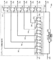
図24は、特許文献1に示される第1の提案のシリアルパラレル変換回路の構成を表わしたものである。このシリアルパラレル変換回路100は、互いに同一構造の第1〜第7の1対2DEMUX(De-Multiplexer)モジュール101〜107をツリー状の多段構造となるように接続している。これら第1〜第7の1対2DEMUXモジュール101〜107は、それぞれ1本の信号をより低速な複数の低速デジタル信号に変換して出力する基本モジュールである。これらの基本モジュールは、データ入力端子Dinとクロック入力端子CLKinを入力側に備え、出力側には第1および第2のデータ出力端子D0、D1と、クロック出力端子CLK2を備えている。
【0005】
第1の1対2DEMUXモジュール101のデータ入力端子Dinには入力データ111が供給され、クロック入力端子CLKinには入力クロック112が供給される。その第1のデータ出力端子D0は第2段目の第2の1対2DEMUXモジュール102のデータ入力端子Dinに接続され、第2のデータ出力端子D1は同じく第2段目の第3の1対2DEMUXモジュール103のデータ入力端子Dinに接続されるようになっている。第1の1対2DEMUXモジュール101のクロック出力端子CLK2は、第2および第3の1対2DEMUXモジュール102、103のクロック入力端子CLKinに接続されている。以下同様であり、第2の1対2DEMUXモジュール102の出力側は第4および第5の1対2DEMUXモジュール104、105の入力側に接続され、第3の1対2DEMUXモジュール103の出力側は第6および第7の1対2DEMUXモジュール106、107の入力側に接続されている。
【0006】
この図24に示したシリアルパラレル変換回路100の動作を次に説明する。入力データ111は高速シリアル入力データである。入力クロック112はこれと同期した高速のクロックである。第1の1対2DEMUXモジュール101は入力データ111を半分のレートの2個のパラレルデータに変換し、第1または第2のデータ出力端子D0、D1のうちのそれぞれ対応するものに出力する。このとき第1の1対2DEMUXモジュール101のクロック出力端子CLK2からは入力クロック112の半分のレートのクロックが出力される。
【0007】
第2段目の第2の1対2DEMUXモジュール102および第3の1対2DEMUXモジュール103は、同様に、第1の1対2DEMUXモジュール101が出力したデータとクロックを、さらに半分のレートの2個のパラレルデータと半分のレートのクロックに変換する。第3段目の第4〜第7の1対2DEMUXモジュール104〜107も同様に、入力されたデータとクロックを、更に半分のレートの2個ずつのパラレルデータと同じく更に半分のレートのクロックに変換する。このように変換した最終データ121〜128は、高速のシリアル入力データ111を1対8の比率で低速パラレルデータに変換したデータとなっている。出力クロック129は、これら最終データ121〜128と同期したクロックである。
【0008】
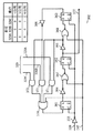
図25は、特許文献2に示される第2の提案のシリアルパラレル変換回路の構成を表わしたものである。このシリアルパラレル変換回路140は、第1段目に配置された第1の1対2シリアルパラレル変換回路141と、第2段目に配置された第2〜第5の1対2シリアルパラレル変換回路142〜145と、第2段目に配置された第1および第2のフリップフロップ回路(F/F)151、152と、これら第2〜第5の1対2シリアルパラレル変換回路142〜145と、第1および第2のフリップフロップ回路151、152の出力側に配置されたリタイミング回路153および入力クロック154を分周する分周回路部155ならびに分周回路部155の所定の端子とアースの間に配置されたオン・オフスイッチ156とによって構成されている。
【0009】
図26は、図25に示した第1の1対2シリアルパラレル変換回路の具体的な回路構成を示したものである。第2〜第5の1対2シリアルパラレル変換回路142〜145も第1の1対2シリアルパラレル変換回路141と同一の回路構成となっているので、これらの回路の図示および説明は省略する。第1の1対2シリアルパラレル変換回路141は、第1〜第3のフリップフロップ回路161〜163と、入力クロック164を反転させるインバータ回路165から構成されている。入力データ166は第1および第2のフリップフロップ回路161、162の入力端子Dに入力され、第1のフリップフロップ回路161の出力端子Qの出力167が第3のフリップフロップ回路163の入力端子Dに入力されるようになっている。入力クロック164は第1のフリップフロップ回路161のクロック入力端子Cに入力される。インバータ回路165によって論理を反転されたクロック168は第2および第3のフリップフロップ回路162、163のクロック入力端子Cに入力される。この第1の1対2シリアルパラレル変換回路141では、第2および第3のフリップフロップ回路162、163から2個のパラレルデータ171、172が出力されることになる。
【0010】
図25に戻ってシリアルパラレル変換回路140の動作を説明する。高速シリアル入力データ166は第1の1対2シリアルパラレル変換回路141に入力され、半分のレートの2個のパラレルデータ171、172(図26参照)に変換される。このうちの一方のパラレルデータ171は、第2および第3の1対2シリアルパラレル変換回路142、143と第1のフリップフロップ回路151に入力される。他方のパラレルデータ172は、第4および第5の1対2シリアルパラレル変換回路144、145と第2のフリップフロップ回路152に入力される。ここで第2および第4の1対2シリアルパラレル変換回路142、144の動作クロック173は、入力クロック154を分周回路155によって分周したものである。第3および第5の1対2シリアルパラレル変換回路143、145の動作クロック174は、入力クロック154を分周回路155によって分周したものである。第1および第2のフリップフロップ回路151、152の動作クロック175は、入力クロック154を分周回路155によって分周したクロックである。
【0011】
分周回路155から出力される各動作クロック173〜175は、周波数は同じであるが、位相が互いに異なっている。分周回路155には、オン・オフスイッチ156が接続されている。オン・オフスイッチ156は、これをオンの状態あるいはオフの状態に設定することで、分周回路155に対して2種類の分周比で入力クロック154を分周し、各動作クロック173〜175を出力することができるようになっている。第2〜第5の1対2シリアルパラレル変換回路142〜145および第1、第2のフリップフロップ回路151、152の出力データ181〜186は、リタイミング回路153で動作クロック173によってリタイミングされる。この結果、パラレルデータ187が出力される。リタイミング用に用いられた動作クロック173は、出力クロックとして出力される。この動作クロック173はパラレルデータ187と同期している。
【0012】
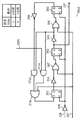
図27は、特許文献3に示される第3の提案としてのパラレルシリアル変換回路の構成を表わしたものである。このパラレルシリアル変換回路200は、6対1のパラレルシリアル変換を行うもので、パラレルシリアル変換部201と、6分周回路202で構成されている。パラレルシリアル変換部201は、エラスティックストア回路(ES)211と、リタイミングを行うリタイミング回路212と、タイミングパルスを発生するタイミングパルス発生回路213と、リタイミング後のパラレルデータをシリアルデータに変換する6対1パラレルシリアル変換回路214から構成されている。
【0013】
このパラレルシリアル変換回路200の動作を説明する。エラスティックストア回路211には第1〜第6の入力データ221〜226がパラレルな入力データとして供給されており、書き込みクロック227に同期してエラスティックストア回路211への書き込みが行われる。エラスティックストア回路211に書き込まれたパラレルデータは、6分周回路202によって入力クロック228を6分周した読み出しクロック229によって読み出される。読み出されたパラレルデータ231は、リタイミング回路212でリタイミングされる。リタイミングされたパラレルデータ232は、タイミングパルス発生回路213によって生成されたタイミングパルス233に基づいて、6対1パラレルシリアル変換回路214でシリアル出力データ235に変換され、出力される。
【0014】
【特許文献1】
特開平11−98101号公報(第0016、0017段落、図4、図5)
【特許文献2】
特開2002−217742号公報(第0013〜第0015段落、図1)
【特許文献3】
特開平8−65173号公報(第0016〜0019段落、図1)
【0015】
【発明が解決しようとする課題】
しかしながら、図24に示した第1の提案のシリアルパラレル変換回路100では、第1の1対2DEMUXモジュール101に代表される1対2DEMUXモジュール101〜107をツリー状に多段に接続している。そして、ツリー構造の各段でそれぞれ1対2、1対4、1対8あるいは1対16といった特定の比率でシリアルデータをパラレルデータに変換している。したがって、このように2の階乗となる比率でシリアルパラレル変換を行うことが可能な一方、これ以外の比率ではシリアルデータをパラレルデータに変換することができないという問題がある。
【0016】
図27に示した第3の提案でも、予め定められた分周比で分周する分周回路を用いている。このためシリアルデータに変換する元となる低速のパラレルデータの本数がその分周回路で入力するパラレルデータの本数によって1通りに決まってしまうという問題がある。この結果、例えば、4対1と5対1の2つの異なった比のパラレルシリアル変換を行うような場合、それぞれの比に個別に対応する合計2種類のパラレルシリアル変換回路を設計する必要があり、設計量が増大するという問題がある。
【0017】
一方、図25および図26に示した第2の提案では、オン・オフスイッチ156をオンまたはオフ状態に設定することで、2通りの分周比を設定することができる。しかも、1個の回路を設計することで、オン・オフスイッチ156の状態の数としての2種類の比でシリアルパラレル変換が可能となるという長所がある。しかしながら、この第2の提案では、分周回路155から複数の分周クロックを発生させている。このため、分周クロック間のスキューに注意が必要である。例えば、分周クロック間でデータの乗せ替えが発生する箇所では第1および第2のフリップフロップ回路151、152のセットアップと保持(ホールドタイム)が厳しくなる可能性がある。そこで、十分にこれらの時間に余裕があることを確認する必要がある。したがって、この分だけ、設計難易度が難しくなるという問題がある。
【0018】
そこで本発明の目的は、各種の比でパラレルシリアル変換あるいはシリアルパラレル変換を行うことのできるデータ形式変換回路を提供することにある。
【0019】
【課題を解決するための手段】
本発明では、(イ)変換対象のシリアルデータに同期した入力クロックを所定の分周比設定情報に応じて複数通りに設定して分周し1本の信号線に出力クロックとして出力可能な分周手段と、(ロ)この分周手段の分周比を前記した分周比設定情報を用いて予め定めた複数通りのうちの任意の1つに設定する分周比設定手段と、(ハ)前記したシリアルデータを前記した入力クロックのタイミングで順番にシフトするデータシフト手段と、このデータシフト手段の出力データを前記した分周手段によって分周したクロックでリタイミングするリタイミング手段とを備え、前記した変換対象のシリアルデータを前記した分周比設定手段の設定した分周比に応じたビット数のパラレルデータに変換するシリアルパラレル変換手段と、(ニ)前記したリタイミング手段でリタイミングする前の前記したデータシフト手段の出力データと外部から設定した同期パターンとを比較する同期パターン検出手段と、(ホ)この同期パターン検出手段が同期パターンを検出したタイミングで前記した分周手段をリセットして前記した入力クロックの分周を開始させるリセット手段と、(ヘ)前記したシリアルパラレル変換手段の変換後のパラレルデータを前記した分周手段の前記した出力クロックに同期して出力するパラレルデータ出力手段とをデータ形式変換回路が具備する。
【0020】
また本発明では、(イ)入力されるシリアルデータを所定の入力クロックに同期して所定のビット数のパラレルデータに変換する初段シリアルパラレル変換部と、(ロ)この初段シリアルパラレル変換部によって変換されたそれぞれのパラレルデータを構成する1ビットずつのデータの連続からなるシリアルデータごとに用意され、前記した入力クロックを所定の分周比設定情報に応じて複数通りに設定して分周し1本の信号線に出力クロックとして出力可能な分周手段と、この分周手段の分周比を前記した分周比設定情報を用いて予め定めた複数通りのうちの任意の1つに設定する分周比設定手段と、前記したシリアルデータを前記した入力クロックのタイミングで順番にシフトするデータシフト手段と、このデータシフト手段の出力データを前記した分周手段によって分周したクロックでリタイミングするリタイミング手段とを備え、前記した入力されるシリアルデータを前記した分周比設定手段の設定した分周比に応じたビット数のパラレルデータに変換する次段シリアルパラレル変換手段と、前記したリタイミング手段でリタイミングする前の前記したデータシフト手段の出力データと外部から設定した同期パターンとを比較する同期パターン検出手段と、この同期パターン検出手段が同期パターンを検出したタイミングで前記した分周手段をリセットして前記した入力クロックの分周を開始させるリセット手段と、前記した次段シリアルパラレル変換手段の変換後のパラレルデータを前記した分周手段の前記した出力クロックに同期して出力するパラレルデータ出力手段とを備えた次段シリアルパラレル変換部とをデータ形式変換回路が具備し、それぞれの次段シリアルパラレル変換部の出力するパラレルデータを併せて前記した出力クロックに同期したパラレルデータとすることにしている。
【0021】
更に本発明では、(イ)出力するシリアルデータに同期する出力用同期クロックを所定の分周比設定情報に応じて複数通りに設定して分周し1本の信号線に出力クロックとして出力可能な分周手段と、この分周手段の分周比を前記した分周比設定情報を用いて予め定めた複数通りのうちの任意の1つに設定する分周比設定手段と、この分周比設定手段の設定した分周比に応じたビット数のパラレルデータを取り込むパラレルデータ取り込み手段と、このパラレルデータ取り込み手段の取り込んだ前記したパラレルデータを前記した分周手段の出力する出力クロックでリタイミングするリタイミング手段と、このリタイミング手段でリタイミングしたパラレルデータを前記した出力用同期クロックに同期させてシリアルデータに変換して出力するパラレルシリアル変換手段とを備えた複数のパラレルシリアル変換部と、(ロ)これらパラレルシリアル変換部のそれぞれ出力するシリアルデータをパラレルに入力してシリアルデータとして出力する次段パラレルシリアル変換部とをデータ形式変換回路が具備する。
【0022】
更にまた本発明では、(イ)出力するシリアルデータに同期する出力用同期クロックを所定の分周比設定情報に応じて複数通りに設定して分周し1本の信号線に出力クロックとして出力可能な分周手段と、この分周手段の分周比を前記した分周比設定情報を用いて予め定めた複数通りのうちの任意の1つに設定する分周比設定手段と、この分周比設定手段の設定した分周比に応じたビット数のパラレルデータを取り込むパラレルデータ取り込み手段と、このパラレルデータ取り込み手段の取り込んだ前記したパラレルデータを前記した分周手段の出力する出力クロックでリタイミングするリタイミング手段と、このリタイミング手段でリタイミングしたパラレルデータを前記した出力用同期クロックに同期させてシリアルデータに変換して出力するパラレルシリアル変換手段とを備え、これらをツリー構造に配置した複数のパラレルシリアル変換部と、(ロ)これら複数のパラレルシリアル変換部の前記したツリー構造の頂点側端部に位置する2以上のパラレルシリアル変換部のそれぞれ出力するシリアルデータをパラレルに入力してシリアルデータとして出力する頂点パラレルシリアル変換部とをデータ形式変換回路が具備する。
【0044】
【発明の実施の形態】
【0045】
【実施例】
以下実施例につき本発明を詳細に説明する。
【0046】
<第1の実施例>
【0047】
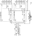
図1は本発明のデータ形式変換回路の第1の実施例としてのシリアルパラレル変換回路を示したものである。このシリアルパラレル変換回路300は、シリアルパラレル変換回路部301と、分周回路部302とによって構成されている。この第1の実施例のシリアルパラレル変換回路300は、シリアルパラレル変換回路部301をデータシフト回路311とリタイミング回路312で構成している。データシフト回路311は、第1〜第6のフリップフロップ回路321〜326を縦続接続した構造となっており、第1のフリップフロップ回路321のデータデータ入力端子Dに入力データ327を供給し、これを入力クロック328によって順次シフトさせるようになっている。この入力クロック328は分周回路部302にも供給され、分周比設定信号329によって分周比を各種設定できるようになっている。
【0048】
リタイミング回路312は同じく第1〜第6のフリップフロップ回路331〜336を備えており、分周回路部302の出力する出力クロック337をそれらのクロック入力端子Cに入力するようになっている。また、リタイミング回路312の第1のフリップフロップ回路331は、データシフト回路311の第1のフリップフロップ回路321の出力端子Qから次段の第2のフリップフロップ回路322のデータ入力端子Dに供給するデータ341をそのデータ入力端子Dに入力するようになっている。また、第2のフリップフロップ回路332は、データシフト回路311の第2のフリップフロップ回路322の出力端子Qから次段の第3のフリップフロップ回路323のデータ入力端子Dに供給するデータ342をそのデータ入力端子Dに入力するようになっている。以下同様である。第6のフリップフロップ回路336の場合には、データシフト回路311の第6のフリップフロップ回路326の出力端子Qから出力されるデータ346をそのデータ入力端子Dに入力するようになっている。
【0049】
このシリアルパラレル変換回路300では、外部から入力されたシリアルな入力データ327とこれに同期した入力クロック328がシリアルパラレル変換回路部301に供給される。入力データ327はデータシフト回路311内の第1〜第6のフリップフロップ回路321〜326を順番にシフトしていく。入力クロック328は分周回路部302にも入力される。分周回路部302は、リセット信号347によりリセットされ、分周比設定信号329に対応した分周比で入力クロック328を分周し、分周後の出力クロック337を出力するようになっている。リタイミング回路312内部の第1〜第6のフリップフロップ回路331〜336では、データシフト回路311の各段のフリップフロップ回路321〜326から出力されるデータ341〜346を、出力クロック337の立ち上がりでリタイミングし、リタイミング回路312の第1〜第6のフリップフロップ回路331〜336の出力端子Qから出力データ351〜356を出力するようになっている。
【0050】
図2は、図1に示した分周回路部の具体的な構成を表わしたものである。この分周回路部302は、第1〜第3のフリップフロップ回路361〜363と、これらのそれぞれ出力端子Qに接続された第1〜第3のインバータ364〜366と、第1および第2のインバータ364、365のそれぞれの出力側に一方の入力側を接続したノア(NOR)回路367、368と、第2のインバータ365または第3のインバータ366の出力側に接続された第1〜第3のアンド(AND)回路371〜373と、これらのアンド回路371〜373の出力側に入力側を配置し、出力側を第1のフリップフロップ回路361の入力端子Dに接続したオア(OR)回路374と、第1のフリップフロップ回路361のクロック入力端子Cに入力クロック328の論理が反転したものを入力する第4のインバータ375から構成されている。
【0051】
この分周回路部302は、入力クロック328の立ち下がりに同期して入力クロック328を分周する回路であり、分周比設定信号329A〜329Cの設定に対応して、分周比が3通りに変化するようになっている。すなわち、分周比設定信号329Aが“1”、分周比設定信号329Bが“0”、分周比設定信号329Cが“0”と設定すれば、4分周回路となる。
【0052】
また、分周比設定信号329Aが“0”、分周比設定信号329Bが“1”、分周比設定信号329Cが“0”と設定すれば、5分周回路となる。分周比設定信号329Aが“0”、分周比設定信号329Bが“0”、分周比設定信号329Cが“1”と設定すれば、6分周回路となる。
【0053】
図3は、図1に示した分周回路の他の例を示したものである。図2と同一部分には同一の符号を付しており、これらの説明を適宜省略する。この分周回路部302Aでは、第2のインバータ365の出力を2入力の第1および第2のアンド回路371A、372Aの一方の入力端子に入力している。第1のアンド回路371Aの他方の入力端子には分周比設定信号329A(図2参照)が入力されるようになっている。第2のアンド回路372Aの他方の入力端子には第3のインバータ366の反転後の出力が供給されるようになっている。オア回路374Aは、これら第1および第2のアンド回路371A、372Aの出力の論理和をとってその出力を第1のフリップフロップ回路361のデータ入力端子Dに供給する。
【0054】
このような分周回路部302Aでは、分周比設定信号329Aの設定に応じて、分周比が2通りに変化する。すなわち、分周比設定信号329Aが“1”に設定されていれば4分周回路となる。分周比設定信号329Aが“0”に設定されていれば5分周回路となる。
【0055】
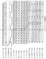
図4は、分周回路の分周比が6で1対6のシリアルパラレル変換動作を行う場合の各種タイミングを示したものである。これは、図2に示した分周回路部302を使用した場合である。これに対して、図5は分周回路の分周比が5で1対5のシリアルパラレル変換動作を行った場合を示している。更に、図6は分周回路の分周比が4で1対4のシリアルパラレル変換動作を行った場合を示している。図5および図6は図2に示した分周回路部302と図3に示した分周回路部302Aの双方を使用することができる。
【0056】
所定の時刻に図1に示すリセット信号347を信号“1”から信号“0”に変化させると(図4(c)、図5(c)、図6(c))、図2に示した分周回路部302あるいは図3に示した分周回路部302A(以下、説明を簡単にするために図2に示した分周回路部302を中心として説明を行い、図3に示した分周回路部302の説明は適宜省略する。)は入力クロック328(図4(b)、図5(b)、図6(b))の分周を開始する。これにより、入力クロック328の最初の立ち下りで、出力クロック337(図4(d)、図5(d)、図6(d))が立ち上がる。以下、図4〜図6に示すように、出力クロック337として図4の場合には入力クロック328の6周期分のクロックが出力され、図5の場合には入力クロック328の5周期分のクロックが出力され、図6の場合には入力クロック328の4周期分のクロックが出力されることになる。
【0057】
このような分周回路部302におけるシリアルパラレル変換回路300の全体的な動作を、同じく図4〜図6を用いて説明する。図4(a)、図5(a)、図6(a)に示す入力データ327は、図1に示すデータシフト回路311で入力クロック328に応じてシフトする。この結果、第1〜第6のフリップフロップ回路321〜326(図1)のそれぞれの出力端子Qから出力されるデータ341〜346(図4(e)〜(j)、図5(e)〜(j)、図6(e)〜(j))は、入力クロック328の立ち上がりのタイミングで1クロックずつシフトしていく(図4(a)、図5(a)、図6(a)の入力データ327に付した符号a、b、c、……参照。)。このようなデータ341〜346は、リタイミング回路312に入力され、出力クロック337の立ち上がりでリタイミングする。このようにして出力データ351〜356(図4(k)〜(p)、図5(k)〜(p)、図6(k)〜(p))が出力されることになる。
【0058】
ここで、図4では、出力データ351〜356が入力データ327を1対6にシリアルパラレル変換したデータとなっており、図5では、出力データ351〜356が入力データ327を1対5にシリアルパラレル変換したデータとなっている。図6では、出力データ351〜356が入力データ327を1対4にシリアルパラレル変換したデータとなっている。
【0059】
図4の6分周の場合を具体的に説明する。たとえば破線で示した時刻t1に着目する。同図(a)に示す入力データ327が“a”、“b”、…、“f”というデータで順に構成されていたとする。これらは第1〜第6のフリップフロップ回路321〜326で順にシフトされる結果、時刻t1には第1のフリップフロップ回路321からデータ“f”が出力されており、第2のフリップフロップ回路322からはデータ“e”が出力されている。以下、同様にして第6のフリップフロップ回路326からはデータ“a”が出力されている。これらのデータ“f”、“e”、…、“a”は、6分周クロックとしての出力クロック337の立ち上がりで第1〜第6のフリップフロップ回路331〜336に取り込まれる。この結果、次の出力クロック337が出力されるまでの出力クロック337の1周期の間、第1〜第6のフリップフロップ回路331〜336の出力端子Qから出力データ351〜356としてデータ“f”、“e”、…、“a”がパラレルに出力される。
【0060】
図5の5分周の場合についても、たとえば破線で示した時刻t2に着目する。同図(a)に示す入力データ327が“a”、“b”、…、“e”というデータで順に構成されていたとする。これらは第1〜第5のフリップフロップ回路321〜325で順にシフトされる結果、時刻t2には第1のフリップフロップ回路321からデータ“e”が出力されており、第2のフリップフロップ回路322からはデータ“d”が出力されている。以下、同様にして第5のフリップフロップ回路325からはデータ“a”が出力されている。これらのデータ“e”、“d”、…、“a”は、5分周クロックとしての出力クロック337の立ち上がりで第1〜第5のフリップフロップ回路331〜335に取り込まれる。この結果、次の出力クロック337が出力されるまでの出力クロック337の1周期の間、第1〜第5のフリップフロップ回路331〜335の出力端子Qから出力データ351〜355としてデータ“e”、“d”、…、“a”がパラレルに出力される。
【0061】
図6の4分周の場合についても、たとえば破線で示した時刻t3に着目する。同図(a)に示す入力データ327が“a”、“b”、…、“d”というデータで順に構成されていたとする。これらは第1〜第4のフリップフロップ回路321〜324で順にシフトされる結果、時刻t3には第1のフリップフロップ回路321からデータ“d”が出力されており、第2のフリップフロップ回路322からはデータ“c”が出力されている。以下、同様にして第4のフリップフロップ回路324からはデータ“a”が出力されている。これらのデータ“d”、“c”、…、“a”は、4分周クロックとしての出力クロック337の立ち上がりで第1〜第4のフリップフロップ回路331〜334に取り込まれる。この結果、次の出力クロック337が出力されるまでの出力クロック337の1周期の間、第1〜第4のフリップフロップ回路331〜334の出力端子Qから出力データ351〜354としてデータ“d”、“c”、…、“a”がパラレルに出力される。
【0062】
このように、本実施例の分周回路部302は、外部から設定した分周比設定信号329に対応して分周比が変わるので、1個のシリアルパラレル変換回路を設計するだけで、パラレル側データ本数が複数通りの場合でも動作することができる。したがって、それぞれの本数に応じてシリアルパラレル変換回路を設計する必要がなく、大幅に設計量を削減することができる。
【0063】
更にこの実施例では、入力クロック327と1本の分周クロック337のみで動作する単純な構成となっているので、シリアルパラレル変換回路300の設計が非常に容易になる。
【0064】
<第1の実施例の変形例>
【0065】
図7は、第1の実施例についての変形例を示したものである。図7で図1と同一部分には同一の符号を付しており、これらの説明を適宜省略する。この変形例のシリアルパラレル変換回路300Aでは、図1に示したシリアルパラレル変換回路部301と、分周回路部302の間に同期パターン検出回路部303を配置した構成となっている。
【0066】
同期パターン検出回路部303は、データシフト回路311を構成する第1〜第6のフリップフロップ回路321〜326の出力端子Qからそれぞれ出力されるデータ341〜346と、外部から入力する同期パターン設定信号381が入力される。この同期パターン検出回路部303は、データ341〜346と同期パターン設定信号381が一致した場合に、リセット信号347Aを出力するようになっている。この結果、分周回路部302からは出力クロック337Aが出力され、リタイミング回路312に供給されることになる。
【0067】
図8は同期パターン検出回路部の具体的な構成を示したものである。同期パターン検出回路部303は、第1〜第5のイクスルーシブ−ノア(EX−NOR)回路391〜395と、これらの出力側に配置された5入力アンド回路396とによって構成されている。第1のイクスルーシブ−ノア回路391には、データ341と同期パターン設定信号381を構成するパラレルデータの第1ビット目の信号381Aが入力されるようになっている。第2のイクスルーシブ−ノア回路392には、データ342と同期パターン設定信号381を構成するパラレルデータの第2ビット目の信号381Bが入力されるようになっている。以下同様にして、第5のイクスルーシブ−ノア回路395には、データ345と同期パターン設定信号381を構成するパラレルデータの第5ビット目の信号381Eが入力されるようになっている。5入力アンド回路396の出力がリセット信号347Aとなる。
【0068】
図9は、図7に示したシリアルパラレル変換回路の各部の動作を示したものである。図9で図5と同一部分には同一の符号を付しており、これらの説明を適宜省略する。この図ではシリアルパラレル変換回路300Aの分周比が“5”の1対5シリアルパラレル変換動作時のタイミングを示している。この例では図9(e)〜(h)に示すようにデータ341〜344(データ“f”〜“c”)が同期パターン設定信号381A〜381Dのそれぞれ対応するものと信号状態が一致した時点でリセット信号347Aが信号“1”となる。ここでデータ“a”、“b”、……は共に信号“1”または“0”の2値の信号である。
【0069】
すなわち、同期パターン検出回路部303は、信号“1”と信号“0”の任意の組み合わせからなる4ビットの同期パターンを同期パターン設定信号381A〜381Dによって設定されている。そして、この4ビットの同期パターンと一致する4ビットデータ“f”〜“c”がデータシフト回路311の出力するデータ341〜344(図9(e)〜(h))としてシフトしてきた時点で、図9(c)に示すようにリセット信号347Aを信号“1”とする。分周回路部302はリセット信号347Aが信号“1”となったときリセットされる。この結果、入力クロック328(図9(b))の立ち下がりのタイミングで出力クロック337Aは信号“0”となり、次の立ち下がりのタイミングで信号“1”となる。データ341〜346(図9(e)〜(j))を、リタイミング回路312によって出力クロック337Aの立ち上がりのタイミングでリタイミングした結果、同期パターン“f”〜“c”が整列され、出力データ352〜355にデータ“f”〜“c”が出力される。このとき、残りの出力データ351としてデータ“g”が出力される。これら出力データ351〜355が入力データ327を1対5シリアルパラレル変換した結果である。
【0070】
このように、この変形例では、分周回路部302のリセット信号347Aを利用し、同期パターン検出回路303を追加するだけで、同期パターンを整列させて出力データに出力することができる。
【0071】
<第2の実施例>
【0072】
図10は、本発明の第2の実施例のシリアルパラレル変換回路を示したものである。この第2の実施例のシリアルパラレル変換回路400では、入力データ327と入力クロック328をまず1対2シリアルパラレル変換回路部401に入力するようになっている。1対2シリアルパラレル変換回路部401は、入力データ327をシリアルパラレル変換して2個のパラレル出力データ402、403と、出力クロック404を出力する。このうち、第1のパラレル出力データ402は第1のシリアルパラレル変換回路部411に供給され、第2のパラレル出力データ403は第2のシリアルパラレル変換回路部412に供給される。出力クロック404はこれら第1および第2のシリアルパラレル変換回路部411、412にクロック信号として供給される他、分周回路部413にもクロック信号として供給されるようになっている。
【0073】
第1および第2のシリアルパラレル変換回路部411、412は第1の実施例の図1に示したシリアルパラレル変換回路部301と同一の回路構成となっている。また、分周回路部413は第1の実施例の分周回路部302と同一の回路構成となっている。すなわち、分周された後の第1のパラレル出力データ402は第1のシリアルパラレル変換回路部411内のデータシフト回路311に入力され、図1に示した第1〜第6のフリップフロップ回路331〜336から出力されるデータ341〜346がリタイミング回路312に入力されて、分周回路部413の出力する出力クロック414(第1の実施例の出力クロック337に相当。)の立ち上がりでリタイミングする。そして、リタイミング回路312の図1に示した第1〜第6のフリップフロップ回路331〜336の出力端子Qから出力データ421〜426(図1における出力データ351〜356に相当。)を出力するようになっている。
【0074】
同様に分周された後の第2のパラレル出力データ403は第2のシリアルパラレル変換回路部412内のデータシフト回路311に入力され、図1に示した第1〜第6のフリップフロップ回路331〜336から出力されるデータ341〜346がリタイミング回路312に入力されて、分周回路部413の出力する出力クロック414(第1の実施例の出力クロック337に相当。)の立ち上がりでリタイミングする。そして、リタイミング回路312の図1に示した第1〜第6のフリップフロップ回路331〜336の出力端子Qから出力データ431〜436(図1における出力データ351〜356に相当。)を出力するようになっている。
【0075】
この第2の実施例で分周回路部413は、第1の実施例の図1に示すリセット信号347に相当するリセット信号415を信号“1”から信号“0”に変化させると(図4(c)、図5(c)、図6(c)参照)、出力クロック404の分周を開始する。これは第1の実施例における入力クロック328(図4(b)、図5(b)、図6(b))の分周の開始に相当する。分周回路部413は分周比設定信号416によって分周比を各種設定できるが、これは図1に示した実施例で分周比設定信号329によって分周比を各種設定できるのに相当する。
【0076】
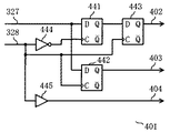
図11は、この第2の実施例における1対2シリアルパラレル変換回路部の具体的な構成を表わしたものである。1対2シリアルパラレル変換回路部401は、入力データ327をデータ入力端子Dに供給する第1および第2のフリップフロップ回路441、442と、第1のフリップフロップ回路441の出力端子Qとデータ入力端子Dを接続した第3のフリップフロップ回路443と、入力クロック328の論理を反転させるインバータ444と所定の時間的な遅延を与える遅延回路445とによって構成されている。インバータ444の出力は第1のフリップフロップ回路441のクロック入力端子Cに供給され、入力クロック328はそのまま第2および第3のフリップフロップ回路442、443のクロック入力端子Cに供給される。この1対2シリアルパラレル変換回路部401では、第3のフリップフロップ回路443の出力端子Qから一方のパラレル出力データ402が出力され、第2のフリップフロップ回路442の出力端子Qから他方のパラレル出力データ403が出力される。また、遅延回路445の出力が出力クロック404となる。
【0077】
この図11に示す1対2シリアルパラレル変換回路部401では入力クロック328の立ち上がりと立ち下がりの双方のタイミングで入力データ327をリタイミングしている。入力クロック328の周波数は、入力データ327の周波数の半分となっている。
【0078】
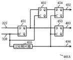
図12は図10のシリアルパラレル変換回路に適用できる他の1対2シリアルパラレル変換回路を示したものである。この1対2シリアルパラレル変換回路部401Aは、入力データ327をそのデータ入力端子Dに入力する第1のフリップフロップ回路451と、第1のフリップフロップ回路451の出力端子Qとデータ入力端子Dをそれぞれ接続した第2および第3のフリップフロップ回路452、453と、第2のフリップフロップ回路452の出力端子Qとデータ入力端子Dを接続した第4のフリップフロップ回路454と、入力クロック328を入力してこれを2分周する2分周回路455とによって構成されている。入力クロック328は第1および第2のフリップフロップ回路451、452のクロック入力端子Cにも供給されるようになっている。また、2分周回路455の分周により得られる出力クロック404は、図10の第1および第2のシリアルパラレル変換回路部411、412に供給される他、第3および第4のフリップフロップ回路453、454のクロック入力端子Cにも供給されるようになっている。
【0079】
この図12に示した1対2シリアルパラレル変換回路部401Aも図11に示した1対2シリアルパラレル変換回路部401と同様に簡単な回路構成となっている。図12の1対2シリアルパラレル変換回路部401Aでは、入力クロック328の立ち上がりのタイミングのみで入力データ327をリタイミングしている。したがって、入力クロック328の周波数は、入力データ327の周波数と等しい。
【0080】
このように図11あるいは図12に示した1対2シリアルパラレル変換回路部401、401Aを使用した図10に示すシリアルパラレル変換回路400では、入力データ327を半分のレートに落としたパラレル出力データ402、403のそれぞれを、シリアルパラレル変換する構成をとっている。このため、構造が単純な1対2シリアルパラレル変換回路部401、401Aのみ高速な入力データ327を処理する必要がある。しかしながら後段の第1および第2のシリアルパラレル変換回路部411、412に入力されるパラレル出力データ402、403は入力データ327の半分のレートとなっている。従って、シリアルパラレル変換回路400の全体では高速動作に適用しやすいという効果が得られる。
【0081】
なお、図10に示す第2の実施例では、入力データ327をまず1対2シリアルパラレル変換回路部401、401Aに入力することにしたが、これは1対2以外の比率のシリアルパラレル変換回路であっても構わない。この場合には、1対2シリアルパラレル変換回路部401、401Aの代わりに配置されるシリアルパラレル変換回路が、多相クロックを用いてデータをリタイミングする構成であっても構わない。更に、外部からの設定により、複数通りの比でシリアルパラレル変換を行うシリアルパラレル変換回路であっても構わない。
【0082】
また、第2の実施例では1段目の1対2シリアルパラレル変換回路部401、401Aと、2段目の第1および第2のシリアルパラレル変換回路部411、412を用いてシリアルパラレル変換回路400を構成したが、3段以上のシリアルパラレル変換回路部を用いてシリアルパラレル変換回路を構成することも可能である。このように、複数のシリアルパラレル変換比を有するシリアルパラレル変換回路部を、多段に接続することで、設計量の更なる削減と、比較的低速で動作する回路部品を一部に使用して高速動作が可能になるという効果が得られる。
【0083】
<第3の実施例>
【0084】
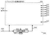
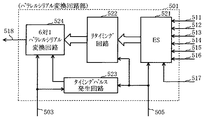
図13は、本発明の第3の実施例のパラレルシリアル変換回路を示したものである。このパラレルシリアル変換回路500は、パラレルシリアル変換回路部501と、分周回路部502とによって構成されている。分周回路部502は第1の実施例における図2あるいは図3に示した分周回路部302、302Aと同一の回路を使用している。入力クロック503は、この分周回路部502とパラレルシリアル変換回路部501の双方に供給される。図1のリセット信号347に相当するリセット信号504が信号“1”から信号“0”に変化すると、図2に示した分周回路部302あるいは図3に示した分周回路部302Aに対応する分周回路部502は入力クロック503(第1の実施例の入力クロック328(図4(b)、図5(b)、図6(b))に相当。)の分周を開始し、分周クロック505(第1の実施例の出力クロック337(図4(d)、図5(d)、図6(d))に相当。)を出力するようになっている。この分周クロック505は、パラレルシリアル変換回路部501に供給される。パラレルシリアル変換回路部501は、パラレルデータとしてのデータ511〜516を入力し、書込クロック517の制御の下でシリアルデータへ変換し、これを出力データ518として出力するようになっている。
【0085】
図14はこのようなパラレルシリアル変換回路部の回路構成の一例を示したものである。パラレルシリアル変換回路部501は図27に示したパラレルシリアル変換部201と同一の構成となっている。パラレルシリアル変換回路部501は、エラスティックストア回路(ES)521と、リタイミングを行うリタイミング回路522と、タイミングパルスを発生するタイミングパルス発生回路523と、リタイミング後のパラレルデータをシリアルデータに変換する6対1パラレルシリアル変換回路524から構成されている。
【0086】
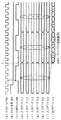
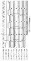
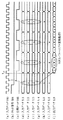
図15〜図17は、このような構成の第3の実施例のパラレルシリアル変換回路の各部の動作状況を表わしたものである。ここで図15は図13に示した分周回路部502の分周比が“6”で6対1パラレルシリアル変換動作時のタイミングを示している。また、図16は分周回路部502の分周比が“5”で5対1パラレルシリアル変換動作時のタイミングを示している。更に、図17は分周回路部502の分周比が“4”で4対1パラレルシリアル変換動作時のタイミングを示している。
【0087】
まず、図2に示した分周回路部302を使用した分周回路部502の分周回路の動作について説明する。図15(c)、図16(c)、図17(c)に示す分周クロック505は、図4(d)、図5(d)、図6(d)において分周回路302が分周した出力クロック337と全く同じタイミングで出力される。
【0088】
次に図13に示した第3の実施例のパラレルシリアル変換回路500の全体的な動作について図15をまず使用して6対1パラレルシリアル変換を行う場合について説明する。入力データ511(同図(d))〜入力データ516(同図(i))は、分周クロック505(同図(c))の立ち上がりでリタイミングされた後、分周クロック505の立ち下がり後の入力クロック503(同図(a))の立ち上がる時刻t11から、順次この入力クロック503に同期してシリアルデータに変換される。図15では、入力データ511、512、513、514、515、516のそれぞれがたとえば“f”、“e”、“d”、“c”、“b”、“a”で示す内容のとき、時刻t11から“a”、“b”、“c”、“d”、“e”、“f”の順番でシリアルに変換されることになる。
【0089】
次に、図16を使用して5対1パラレルシリアル変換を行う場合について説明する。入力データ511(同図(d))〜入力データ515(同図(h))は、分周クロック505(同図(c))の立ち上がりでリタイミングされた後、分周クロック505の立ち下がり後の入力クロック503(同図(a))の立ち上がる時刻t12から、順次この入力クロック503に同期してシリアルデータに変換される。図16では、入力データ511、512、513、514、515のそれぞれがたとえば“f”、“e”、“d”、“c”、“b”で示す内容のとき、時刻t12から“b”、“c”、“d”、“e”、“f”の順番でシリアルに変換されることになる。
【0090】
最後に、図17を使用して4対1パラレルシリアル変換を行う場合について説明する。入力データ511(同図(d))〜入力データ514(同図(g))は、分周クロック505(同図(c))の立ち上がりでリタイミングされた後、分周クロック505の立ち上がった状態の時刻t13から、順次この入力クロック503に同期してシリアルデータに変換される。図17では、入力データ511、512、513、514のそれぞれがたとえば“f”、“e”、“d”、“c”で示す内容のとき、時刻t13から“c”、“d”、“e”、“f”の順番でシリアルに変換されることになる。
【0091】
このように第3の実施例では、図13に示した分周比設定信号506に対応して分周比が変化する分周回路部502をパラレルシリアル変換回路に応用することで、1個のパラレルシリアル変換回路を設計するだけで、パラレル側データの本数が複数通りの場合について動作させることができる。すなわち、それぞれの本数に応じてパラレルシリアル変換回路を設計する必要がなく、大幅に設計量を削減することができる。
【0092】
また、第3の実施例のパラレルシリアル変換回路500は、入力クロック503と1本の分周クロック505のみで動作する単純な構成であるため、非常に設計が容易である。
【0093】
<第4の実施例>
【0094】
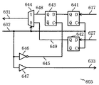
図18は、本発明の第4の実施例のパラレルシリアル変換回路を示したものである。このパラレルシリアル変換回路600は、第1および第2のパラレルシリアル変換回路部601、602と、これらの出力側に配置された2対1パラレルシリアル変換回路部603と、第1および第2のパラレルシリアル変換回路部601、602に分周クロック604を供給する分周回路部605によって構成されている。第1のパラレルシリアル変換回路部601は、パラレルな入力データ611〜616を入力してこれらを第1のシリアルデータに変換して2対1パラレルシリアル変換回路部603に一方のパラレルデータ617として入力するようになっている。また、第2のパラレルシリアル変換回路部602は、パラレルな入力データ621〜626を入力してこれらを第2のシリアルデータに変換して2対1パラレルシリアル変換回路部603に他方のパラレルデータ627として入力するようになっている。2対1パラレルシリアル変換回路部603はこれらパラレルデータ617、627を入力してシリアルデータに変換し、これを出力データ631として出力する一方、入力クロック632の供給を受けてクロック633を第1および第2のパラレルシリアル変換回路部601、602および分周回路部605に供給するようになっている。分周回路部605は、リセット信号634によりリセットされ、分周比設定信号635に対応した分周比でクロック633を分周し、分周クロック604を出力するようになっている。
【0095】
ここで、第1および第2のパラレルシリアル変換回路部601、602は、たとえば第3の実施例のパラレルシリアル変換回路部501(図14)と同一の回路で構成することができる。また、分周回路部605は第1の実施例における図2あるいは図3に示した分周回路部302、302Aと同一の回路を使用することができる。そこで、これらの回路の図示および説明は省略する。
【0096】
図19は、この第4の実施例のパラレルシリアル変換回路の2対1パラレルシリアル変換回路部の具体的な構成を表わしたものである。2対1パラレルシリアル変換回路部603は、一方のパラレルデータ617をデータ入力端子Dに入力する第1のフリップフロップ回路641と、他方のパラレルデータ627をデータ入力端子Dに入力する第2のフリップフロップ回路642と、第1のフリップフロップ回路641の出力端子Qとデータ入力端子Dを接続された第3のフリップフロップ回路643と、第3のフリップフロップ回路643の出力端子Qと一方の入力端子“1”を接続したセレクタ644と、入力クロック632の論理を反転させてこれを反転クロック645として第3のフリップフロップ回路のクロック入力端子Cに供給するインバータ646と、入力クロック632を入力して所定時間遅延させてクロック633を出力する遅延回路647とによって構成されている。
【0097】
入力クロック632はセレクタ644のセレクト端子ならびに第1および第2のフリップフロップ回路641、642のクロック入力端子Cにも供給されるようになっている。セレクタ644の他方の入力端子“0”には第2のフリップフロップ回路642の出力端子Qが接続されている。セレクタ644はセレクト端子に入力される入力クロック632の信号状態に応じて第3のフリップフロップ回路643の出力端子Qから出力されるデータ648あるいは第2のフリップフロップ回路642の出力端子Qから出力されるデータ649の一方を選択して出力データ631として出力するようになっている。
【0098】
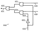
図20は図19に示したセレクタの具体的な回路構成の一例を示したものである。セレクタ644は、入力クロック632とデータ648の論理積をとる第1のアンド回路651と、インバータ652による入力クロック632の反転クロック653とデータ649の論理積をとる第2のアンド回路654と、第1および第2のアンド回路651、654の論理和をとるオア回路655によって構成される。オア回路655から出力データ631が出力されることになる。
【0099】
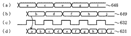
図21は、このセレクタ回路の各部の状態を表わしたものである。同図(a)はセレクタ644(図20)に入力される一方のデータ648を表わし、同図(b)はセレクタ644に入力される他方のデータ649を表わしている。同図(c)に示すように入力クロック632が信号“1”のときには一方のデータ648が選択されて出力データ631として出力される。信号“0”のときには他方のデータ649が選択されて出力データ631として出力されることになる。
【0100】
図22は図21に示したような回路動作を行う他のセレクタの構成を表わしたものである。この図22で図20と同一の部分には同一の符号を付しており、これらの説明を適宜省略する。図22に示したセレクタ644Aでは、図20に示したセレクタ644の第1および第2のアンド回路651、654を第1および第2のナンド(NAND)回路661、662に置き換えており、これらの出力側を図20におけるオア回路655の代わりに第3のナンド回路663に置き換えている。第3のナンド回路663から出力データ631として2つのデータ648、649のいずれかを選択したデータが出力される。
【0101】
図18に示した第4の実施例のパラレルシリアル変換回路600は以上のように構成されているので、第1および第2のパラレルシリアル変換回路部601、602のそれぞれでパラレルな入力データ611〜616、621〜626をシリアルデータ617、627に変換し、更にこれらをシリアルデータとしての出力データ631に変換する。このように2段構成でパラレルデータをシリアルデータに変換しているため、第1段目を構成する第1および第2のパラレルシリアル変換回路部601、602は比較的低速の回路として構成することができる。また、第2段目を構成する2対1パラレルシリアル変換回路部603を簡単な回路とすることができ、高速動作に容易に適応させることができる。
【0102】
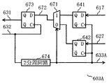
図23は第4の実施例のパラレルシリアル変換回路の2対1パラレルシリアル変換回路部の他の例を表わしたものである。図23で図19と同一部分には同一の符号を付しており、これらの説明を適宜省略する。この2対1パラレルシリアル変換回路部603Aは、第1および第2のフリップフロップ回路641、642の出力側にセレクタ671を配置し、その選択出力672を第3のフリップフロップ回路673のデータ入力端子Dに入力している。入力クロック632は第3のフリップフロップ回路673のクロック入力端子Cに供給される他、2分周回路674に入力されて分周され、これがクロック633Aとしてセレクタ671のセレクト端子ならびに第1および第2のフリップフロップ回路641、642のクロック入力端子Cに供給されるようになっている。
【0103】
先の図19に示した2対1パラレルシリアル変換回路部603では、パラレルデータ617を第1および第3のフリップフロップ回路641、643でリタイミングしたデータ648を、入力クロック632が信号“1”のタイミングで選択して出力し、他方のパラレルデータ627を第2のフリップフロップ回路642でリタイミングしたデータ649を、入力クロック632が“0”のタイミングで選択して出力している。入力クロック632の周波数は、出力データ631の周波数の半分である。
【0104】
図23の構成の2対1パラレルシリアル変換回路部603Aでは、2つのパラレルデータ617、627を、入力クロック632を2分周したクロック633Aでリタイミングし、このクロック633Aで選択した結果を入力クロック632でリタイミングして出力データ631を出力しており、入力クロック632の周波数は、出力データ631の周波数と等しい。
【0105】
このように第4の実施例のパラレルシリアル変換回路600は、第1および第2のパラレルシリアル変換回路部601、602が、出力データ631の半分のレートのデータを出力する構成をとっているため、構造が単純な2対1パラレルシリアル変換回路603のみが高速な出力データ631に対応すればよい。従って、パラレルシリアル変換回路600全体を高速で動作させることができるという効果が得られる。
【0106】
なお、図18に示した第4の実施例では、2対1パラレルシリアル変換回路603から出力データ631を出入力する構成となっているが、2対1以外の比のパラレルシリアル変換回路を使用してもよいことはもちろんである。この場合、図19に示す2対1パラレルシリアル変換回路部603のようにクロックでデータを選択してシリアルデータを出力する構成が、多相クロックでデータを選択する構成であっても構わない。また、外部からの設定により、複数通りの比でパラレルシリアル変換を行う構成のパラレルシリアル変換回路を使用してもよいことも当然である。更に、第4の実施例で用いた2対1パラレルシリアル変換回路603は第1および第2のパラレルシリアル変換回路部601、602を初段とし、2対1パラレルシリアル変換回路部603を2段目とした2段構成の回路として構成しているが、3段以上の回路構成となっていてもよい。
【0107】
以上説明したように複数のパラレルシリアル変換比を有するパラレルシリアル変換回路を、多段に接続することによって、設計量の更なる削減と、高速動作という効果を得ることができる。
【0108】
また、以上説明した実施例あるいは変形例で示したパラレルシリアル変換回路およびシリアルパラレル変換回路は、分周回路で分周したクロックを1本のみ出力させ、この分周クロックと高速クロックのみで動作することにしたので、設計が容易になるという効果が得られる。
【0109】
また、実施例で示したシリアルパラレル変換回路は、分周回路にリセット信号を入力しているため、同期パターン検出回路を追加するだけで、容易に同期パターンをパラレル側データに並べ替えて出力することができるという効果が得られる。
【0110】
なお、以上説明した各実施例および変形例では、フリップフロップ回路、AND回路、OR回路等の個別回路の入力信号と出力信号はすべてシングルの信号で動作することを想定したが、差動信号で動作する差動回路であってもよいことは当然である。
【発明の効果】
以上説明したように本発明によれば、外部等から設定した分周比に対応して分周する分周手段を設けたことにより、1個のシリアルパラレル変換手段あるいはパラレルシリアル変換手段を設計するだけで、パラレル側データ本数が複数通りの場合でも動作することができ、それぞれの本数に応じてシリアルパラレル変換手段を設計する必要がない。したがって、設計量を大幅に削減することができるという効果がある。また、入力クロックと入力クロックを分周した1本の分周クロックのみで動作する単純な回路として構成可能である。したがって、この意味でも設計が非常に容易になる。
【0112】
また、本発明によれば、シリアルパラレル変換手段あるいはパラレルシリアル変換手段を複数段で構成したので、高速のデータ形式変換回路を構成する場合でも一部の回路部分を高速用の回路構成とすればよく、全体的な回路のコストダウンを図ることができるだけでなく、回路の高速化にも対処しやすいという効果がある。また、回路として同一回路部分を重複して使用可能なので、設計量の更なる削減と設計時間の短縮を図ることができる。
【図面の簡単な説明】
【図1】本発明の第1の実施例におけるシリアルパラレル変換回路のブロック図である。
【図2】図1に示した分周回路部の具体的な構成を表わした回路図である。
【図3】図1に示した分周回路の他の例を示した回路図である。
【図4】第1の実施例の分周回路で1対6のシリアルパラレル変換動作を行う場合の各部を示すタイミング図である。
【図5】第1の実施例の分周回路で1対5のシリアルパラレル変換動作を行う場合の各部を示すタイミング図である。
【図6】第1の実施例の分周回路で1対4のシリアルパラレル変換動作を行う場合の各部を示すタイミング図である。
【図7】第1の実施例の変形例におけるシリアルパラレル変換回路のブロック図である。
【図8】図7における同期パターン検出回路部の具体的な構成を示した回路図である。
【図9】図7に示したシリアルパラレル変換回路の各部の動作を示すタイミング図である。
【図10】本発明の第2の実施例のシリアルパラレル変換回路を示した概略構成図である。
【図11】第2の実施例における1対2シリアルパラレル変換回路の具体的な構成を表わした回路図である。
【図12】図10のシリアルパラレル変換回路に適用できる他の1対2シリアルパラレル変換回路を示した回路図である。
【図13】本発明の第3の実施例のパラレルシリアル変換回路を示したブロック図である。
【図14】第3の実施例のパラレルシリアル変換回路部の回路構成の一例を示した概略構成図である。
【図15】第3の実施例のパラレルシリアル変換回路で6対1パラレルシリアル変換動作を表わしたタイミング図である。
【図16】第3の実施例のパラレルシリアル変換回路で5対1パラレルシリアル変換動作を表わしたタイミング図である。
【図17】第3の実施例のパラレルシリアル変換回路で4対1パラレルシリアル変換動作を表わしたタイミング図である。
【図18】本発明の第4の実施例のパラレルシリアル変換回路を示した概略構成図である。
【図19】第4の実施例のパラレルシリアル変換回路の2対1パラレルシリアル変換回路部の具体的な構成を表わした回路図である。
【図20】図19に示したセレクタ回路の具体的な回路構成の一例を示した回路図である。
【図21】図20に示したセレクタ回路の各部の状態を示すタイミング図である。
【図22】図20に示したセレクタ回路の他の例を示した回路図である。
【図23】第4の実施例のパラレルシリアル変換回路の2対1パラレルシリアル変換回路部の他の構成を表わした回路図である。
【図24】従来行われた第1の提案のシリアルパラレル変換回路の構成を表わしたブロック図である。
【図25】従来行われた第2の提案のシリアルパラレル変換回路の構成を表わしたブロック図である。
【図26】図25に示した第1のシリアルパラレル変換回路の具体的な回路構成を示した回路図である。
【図27】従来行われた第3の提案としてのパラレルシリアル変換回路の構成を表わしたブロック図である。
【符号の説明】
300、400 シリアルパラレル変換回路
301 シリアルパラレル変換回路部
302、302A、413、502、605 分周回路部
303 同期パターン検出回路部
311 データシフト回路
312、522 リタイミング回路
327、511〜516、611〜616、621〜626 入力データ
328、503、632 入力クロック
329、416、506、635 分周比設定信号
337 出力クロック
347、415、504、634 リセット信号
351〜356、421〜426、431〜436、518、631 出力データ
401、401A 1対2シリアルパラレル変換回路部
411 第1のシリアルパラレル変換回路部
412 第2のシリアルパラレル変換回路部
500、600 パラレルシリアル変換回路
501 パラレルシリアル変換回路部
505 分周クロック
521 エラスティックストア回路
524 6対1パラレルシリアル変換回路
601 第1のパラレルシリアル変換回路部
602 第2のパラレルシリアル変換回路部
603、603A 2対1パラレルシリアル変換回路部[0001]
BACKGROUND OF THE INVENTION
The present invention relates to a data format conversion circuit for converting parallel data or serial data, and more particularly to a data format conversion circuit for converting parallel data to serial data and vice versa.
[0002]
[Prior art]
The progress of LSI (Large Scale Integration) technology is remarkable, the operating clock inside LSI is several hundred MHz (megahertz), and the signal transmission speed between LSIs is several Gbps (gigabit / second) class, Speeding up. On the other hand, the difference between the operation speed inside the LSI and the signal transmission speed between the LSIs is large. Therefore, if a parallel-serial conversion circuit is arranged in the output unit of the LSI and low-speed parallel data in the LSI is converted into high-speed serial data, the high-speed serial data can be output from the LSI to the outside. If a serial / parallel conversion circuit is arranged in the input section of the LSI, it is possible to convert high-speed serial data input from the outside into low-speed parallel data and supply it to the LSI.
[0003]
For this purpose, several serial-parallel conversion circuits for converting serial data into parallel data and parallel-serial conversion circuits for converting parallel data into serial data have been proposed to meet the demand for data input / output between LSI and the outside. (For example,
[0004]
FIG. 24 shows the configuration of the first proposed serial-parallel conversion circuit disclosed in
[0005]
Data input terminal D of first one-to-two
[0006]
Next, the operation of the serial /
[0007]
Similarly, the second one-to-two
[0008]
FIG. 25 shows the configuration of the second proposed serial-parallel conversion circuit disclosed in
[0009]
FIG. 26 shows a specific circuit configuration of the first one-to-two serial / parallel conversion circuit shown in FIG. Since the second to fifth one-to-two serial /
[0010]
Returning to FIG. 25, the operation of the serial-
[0011]
The operation clocks 173 to 175 output from the frequency dividing
[0012]
FIG. 27 shows a configuration of a parallel-serial conversion circuit as a third proposal disclosed in
[0013]
The operation of the parallel-
[0014]
[Patent Document 1]
JP-A-11-98101 (paragraphs 0016 and 0017, FIGS. 4 and 5)
[Patent Document 2]
JP 2002-217742 A (paragraphs 0013 to 0015, FIG. 1)
[Patent Document 3]
JP-A-8-65173 (paragraphs 0016 to 0019, FIG. 1)
[0015]
[Problems to be solved by the invention]
However, in the first proposed serial /
[0016]
The third proposal shown in FIG. 27 also uses a frequency dividing circuit that divides the frequency by a predetermined frequency dividing ratio. For this reason, there is a problem that the number of low-speed parallel data to be converted into serial data is determined in one way depending on the number of parallel data input by the frequency dividing circuit. As a result, for example, when performing parallel-serial conversion at two different ratios of 4 to 1 and 5 to 1, it is necessary to design a total of two types of parallel-serial conversion circuits individually corresponding to each ratio. There is a problem that the design amount increases.
[0017]
On the other hand, in the second proposal shown in FIG. 25 and FIG. 26, two types of frequency division ratios can be set by setting the on / off
[0018]
SUMMARY OF THE INVENTION Accordingly, an object of the present invention is to provide a data format conversion circuit capable of performing parallel-serial conversion or serial-parallel conversion at various ratios.
[0019]
[Means for Solving the Problems]
In the present invention, (a) an input clock synchronized with serial data to be converted is set in a plurality of ways according to predetermined division ratio setting information, divided, and output as an output clock on one signal line. (B) a frequency division ratio setting means for setting the frequency division ratio of the frequency division means to any one of a plurality of predetermined numbers using the frequency division ratio setting information described above; )A data shift means for sequentially shifting the serial data described above at the timing of the input clock; and a retiming means for retiming the output data of the data shift means by the clock divided by the frequency dividing means,The serial data to be convertedAs described aboveSerial / parallel conversion means for converting into parallel data having the number of bits corresponding to the division ratio set by the division ratio setting means;Synchronization pattern detection means for comparing the output data of the data shift means before retiming by the retiming means and a synchronization pattern set externally;)Resetting means for resetting the frequency dividing means at the timing when the synchronous pattern detecting means detects the synchronous pattern and starting the frequency division of the input clock;The parallel data after conversion by the serial / parallel conversion meansAs described aboveThe data format conversion circuit comprises parallel data output means for outputting in synchronization with the output clock of the frequency dividing means.
[0020]
In the present invention, (a) a first-stage serial / parallel conversion unit that converts input serial data into parallel data having a predetermined number of bits in synchronization with a predetermined input clock; and (b) conversion by the first-stage serial / parallel conversion unit. 1 is prepared for each serial data consisting of a series of 1-bit data constituting each parallel data, and the input clock described above is set in a plurality of ways according to predetermined division ratio setting information, and is divided. Frequency dividing means capable of outputting as an output clock to one signal line, and a frequency dividing ratio of the frequency dividing means is set to any one of a plurality of predetermined methods using the frequency division ratio setting information described above. Frequency division ratio setting means, data shift means for sequentially shifting the serial data at the timing of the input clock, and output data of the data shift means Retiming means for retiming with a clock frequency-divided by the frequency dividing means described above, and paralleling the number of bits corresponding to the frequency dividing ratio set by the frequency dividing ratio setting means described above Next-stage serial / parallel conversion means for converting to data, synchronization pattern detection means for comparing the output data of the data shift means before retiming by the retiming means and a synchronization pattern set from the outside, and this synchronization The reset means for resetting the frequency dividing means at the timing when the pattern detecting means detects the synchronization pattern and starting the frequency division of the input clock, and the parallel data after the conversion of the next-stage serial / parallel converting means Parallel data output means for outputting in synchronization with the aforementioned output clock of the frequency dividing means The data format conversion circuit includes a next-stage serial / parallel conversion unit including the parallel data output from each of the subsequent-stage serial / parallel conversion units, and the parallel data is synchronized with the output clock. .
[0021]
Furthermore, in the present invention, (b) an output synchronous clock synchronized with the output serial data can be set in a plurality of ways according to predetermined division ratio setting information and divided to be output as an output clock to one signal line. A frequency dividing means, a frequency dividing ratio setting means for setting a frequency dividing ratio of the frequency dividing means to any one of a plurality of predetermined values using the frequency dividing ratio setting information, and the frequency dividing means. Parallel data fetching means for fetching parallel data of the number of bits corresponding to the frequency division ratio set by the ratio setting means, and the parallel data fetched by the parallel data fetching means are output by the output clock output from the frequency dividing means. Retiming means for timing, and parallel data retimed by the retiming means is converted into serial data in synchronization with the output synchronous clock and output. A plurality of parallel serial conversion units having parallel serial conversion means, and (b) a next-stage parallel serial conversion unit that inputs serial data output from each of these parallel serial conversion units in parallel and outputs the data as serial data. A format conversion circuit is provided.
[0022]
Furthermore, in the present invention, (b) an output synchronous clock synchronized with the output serial data is set in a plurality of ways in accordance with predetermined division ratio setting information, and is divided and output to one signal line as an output clock. Possible frequency dividing means, frequency dividing ratio setting means for setting the frequency dividing ratio of the frequency dividing means to any one of a plurality of predetermined values using the above-described frequency dividing ratio setting information, Parallel data fetching means for fetching parallel data of the number of bits corresponding to the frequency division ratio set by the frequency ratio setting means, and the parallel data fetched by the parallel data fetching means are output clocks output from the frequency dividing means. Retiming means for retiming, and parallel data retimed by the retiming means are converted into serial data in synchronization with the output synchronous clock and output. Parallel serial conversion means, and a plurality of parallel serial conversion units arranged in a tree structure, and (b) two or more of the plurality of parallel serial conversion units positioned at the apex side end of the tree structure described above The data format conversion circuit includes a vertex parallel serial conversion unit that inputs serial data output from the parallel serial conversion unit in parallel and outputs the serial data as serial data.
[0044]
DETAILED DESCRIPTION OF THE INVENTION
[0045]
【Example】
Hereinafter, the present invention will be described in detail with reference to examples.
[0046]
<First embodiment>
[0047]
FIG. 1 shows a serial-parallel conversion circuit as a first embodiment of the data format conversion circuit of the present invention. The serial /
[0048]
Similarly, the
[0049]
In the serial /
[0050]
FIG. 2 shows a specific configuration of the frequency dividing circuit section shown in FIG. The
[0051]
The
[0052]
Further, when the frequency division
[0053]
FIG. 3 shows another example of the frequency dividing circuit shown in FIG. The same parts as those in FIG. 2 are denoted by the same reference numerals, and description thereof will be omitted as appropriate. In the frequency
[0054]
In such a frequency
[0055]
FIG. 4 shows various timings when a 1 to 6 serial-parallel conversion operation is performed with a frequency dividing ratio of 6. This is a case where the frequency
[0056]
When the
[0057]
The overall operation of the serial /
[0058]
Here, in FIG. 4, the
[0059]
The case of dividing by 6 in FIG. 4 will be specifically described. For example, time t indicated by a broken line1Pay attention to. Assume that the
[0060]
Also in the case of dividing by 5 in FIG. 5, for example, the time t shown by a broken line2Pay attention to. Assume that the
[0061]
Also in the case of the divide-by-four in FIG.ThreePay attention to. Assume that the
[0062]
As described above, the
[0063]
Furthermore, in this embodiment, since it has a simple configuration that operates only with the
[0064]
<Modification of the first embodiment>
[0065]
FIG. 7 shows a modification of the first embodiment. In FIG. 7, the same parts as those in FIG. The serial-
[0066]
The synchronization pattern
[0067]
FIG. 8 shows a specific configuration of the synchronization pattern detection circuit unit. The synchronization pattern
[0068]
FIG. 9 shows the operation of each part of the serial-parallel conversion circuit shown in FIG. 9, the same parts as those in FIG. 5 are denoted by the same reference numerals, and description thereof will be omitted as appropriate. This figure shows the timing at the time of the 1 to 5 serial / parallel conversion operation in which the frequency division ratio of the serial /
[0069]
That is, the synchronization pattern
[0070]
Thus, in this modification, the synchronization pattern can be aligned and output to the output data simply by using the
[0071]
<Second embodiment>
[0072]
FIG. 10 shows a serial-parallel conversion circuit according to the second embodiment of the present invention. In the serial /
[0073]
The first and second serial / parallel
[0074]
Similarly, the second
[0075]
In the second embodiment, the
[0076]
FIG. 11 shows a specific configuration of the one-to-two serial / parallel conversion circuit unit in the second embodiment. The one-to-two serial / parallel
[0077]
In the one-to-two serial / parallel
[0078]
FIG. 12 shows another one-to-two serial / parallel conversion circuit applicable to the serial / parallel conversion circuit of FIG. The one-to-two serial / parallel
[0079]
The one-to-two serial / parallel
[0080]
As described above, in the serial /
[0081]
In the second embodiment shown in FIG. 10, the
[0082]
In the second embodiment, the serial / parallel conversion circuit is configured by using the first-stage one-to-two serial / parallel
[0083]
<Third embodiment>
[0084]
FIG. 13 shows a parallel-serial conversion circuit according to a third embodiment of the present invention. The parallel /
[0085]
FIG. 14 shows an example of the circuit configuration of such a parallel-serial conversion circuit unit. The parallel-serial
[0086]
15 to 17 show the operation status of each part of the parallel-serial conversion circuit of the third embodiment having such a configuration. Here, FIG. 15 shows the timing at the time of the 6-to-1 parallel-serial conversion operation when the frequency dividing ratio of the frequency
[0087]
First, the operation of the divider circuit of the
[0088]
Next, the overall operation of the parallel-
[0089]
Next, the case of performing 5 to 1 parallel serial conversion will be described with reference to FIG. The input data 511 (FIG. (D)) to the input data 515 (FIG. (H)) are retimed at the rising edge of the divided clock 505 (FIG. (C)), and then the falling edge of the divided
[0090]
Finally, the case of performing 4-to-1 parallel serial conversion will be described with reference to FIG. Input data 511 (FIG. (D)) to input data 514 (FIG. (G)) are retimed at the rising edge of the divided clock 505 (FIG. (C)), and then the divided
[0091]
As described above, in the third embodiment, by applying the frequency
[0092]
Further, the parallel-
[0093]
<Fourth embodiment>
[0094]
FIG. 18 shows a parallel-serial conversion circuit according to a fourth embodiment of the present invention. The parallel-
[0095]
Here, the first and second parallel / serial
[0096]
FIG. 19 shows a specific configuration of the 2-to-1 parallel-serial conversion circuit portion of the parallel-serial conversion circuit according to the fourth embodiment. The 2-to-1 parallel-serial
[0097]
The
[0098]
FIG. 20 shows an example of a specific circuit configuration of the selector shown in FIG. The
[0099]
FIG. 21 shows the state of each part of the selector circuit. FIG. 10A shows one
[0100]
FIG. 22 shows the configuration of another selector that performs the circuit operation as shown in FIG. In FIG. 22, the same parts as those in FIG. 20 are denoted by the same reference numerals, and description thereof will be omitted as appropriate. In the
[0101]
Since the parallel-
[0102]
FIG. 23 shows another example of the 2-to-1 parallel-serial conversion circuit portion of the parallel-serial conversion circuit according to the fourth embodiment. In FIG. 23, the same parts as those in FIG. In this 2-to-1 parallel-serial
[0103]
In the 2-to-1 parallel-serial
[0104]
In the 2-to-1 parallel-serial
[0105]
As described above, the parallel-
[0106]
In the fourth embodiment shown in FIG. 18, the
[0107]
As described above, by connecting the parallel-serial conversion circuits having a plurality of parallel-serial conversion ratios in multiple stages, the effect of further reducing the design amount and operating at high speed can be obtained.
[0108]
Further, the parallel-serial conversion circuit and the serial-parallel conversion circuit shown in the above-described embodiments or modifications output only one clock divided by the frequency dividing circuit, and operate only with the frequency-divided clock and the high-speed clock. As a result, an effect of facilitating the design can be obtained.
[0109]
Further, since the serial-parallel conversion circuit shown in the embodiment inputs the reset signal to the frequency dividing circuit, the synchronization pattern can be easily rearranged into the parallel-side data and output simply by adding the synchronization pattern detection circuit. The effect that it can be obtained.
[0110]
In each of the embodiments and modifications described above, it is assumed that the input and output signals of individual circuits such as a flip-flop circuit, an AND circuit, and an OR circuit all operate as a single signal. Of course, the differential circuit may operate.
【The invention's effect】
As described above, according to the present invention, one serial / parallel conversion unit or parallel / serial conversion unit is designed by providing a frequency dividing unit that divides the frequency according to a frequency dividing ratio set from the outside. As a result, it is possible to operate even when the number of parallel-side data is plural, and it is not necessary to design serial-parallel conversion means according to each number of data. Therefore, there is an effect that the design amount can be greatly reduced. In addition, the circuit can be configured as a simple circuit that operates with only one divided clock obtained by dividing the input clock and the input clock. Therefore, the design is very easy in this sense.
[0112]
Also bookAccording to the invention, since the serial-parallel conversion means or the parallel-serial conversion means is configured in a plurality of stages, even when a high-speed data format conversion circuit is configured, a part of the circuit portion may be a high-speed circuit configuration. As a result, not only can the cost of the circuit be reduced, but also the speed of the circuit can be easily coped with. In addition, since the same circuit portion can be used as a circuit, the design amount can be further reduced and the design time can be shortened.
[Brief description of the drawings]
FIG. 1 is a block diagram of a serial / parallel conversion circuit according to a first embodiment of the present invention.
FIG. 2 is a circuit diagram showing a specific configuration of a frequency dividing circuit section shown in FIG.
FIG. 3 is a circuit diagram showing another example of the frequency dividing circuit shown in FIG. 1;
FIG. 4 is a timing chart showing each part when a 1: 6 serial / parallel conversion operation is performed in the frequency divider of the first embodiment;
FIG. 5 is a timing chart showing each part when a 1 to 5 serial / parallel conversion operation is performed in the frequency divider of the first embodiment;
FIG. 6 is a timing chart showing each part when a one-to-four serial / parallel conversion operation is performed in the frequency divider of the first embodiment;
FIG. 7 is a block diagram of a serial-parallel conversion circuit in a modification of the first embodiment.
8 is a circuit diagram showing a specific configuration of a synchronization pattern detection circuit unit in FIG. 7;
9 is a timing chart showing the operation of each part of the serial-parallel conversion circuit shown in FIG. 7;
FIG. 10 is a schematic configuration diagram showing a serial-parallel conversion circuit according to a second embodiment of the present invention.
FIG. 11 is a circuit diagram showing a specific configuration of a one-to-two serial-parallel conversion circuit in a second embodiment.
12 is a circuit diagram showing another one-to-two serial / parallel conversion circuit applicable to the serial / parallel conversion circuit of FIG. 10;
FIG. 13 is a block diagram showing a parallel-serial conversion circuit according to a third embodiment of the present invention.
FIG. 14 is a schematic configuration diagram showing an example of a circuit configuration of a parallel-serial conversion circuit unit according to a third embodiment.
FIG. 15 is a timing diagram illustrating a 6-to-1 parallel-serial conversion operation in the parallel-serial conversion circuit according to the third embodiment;
FIG. 16 is a timing diagram illustrating a 5-to-1 parallel-serial conversion operation in the parallel-serial conversion circuit according to the third embodiment;
FIG. 17 is a timing diagram illustrating a 4-to-1 parallel-serial conversion operation in the parallel-serial conversion circuit according to the third embodiment.
FIG. 18 is a schematic configuration diagram showing a parallel-serial conversion circuit according to a fourth embodiment of the present invention.
FIG. 19 is a circuit diagram showing a specific configuration of a 2-to-1 parallel-serial conversion circuit unit of a parallel-serial conversion circuit according to a fourth embodiment.
20 is a circuit diagram showing an example of a specific circuit configuration of the selector circuit shown in FIG. 19;
FIG. 21 is a timing chart showing the state of each part of the selector circuit shown in FIG. 20;
22 is a circuit diagram showing another example of the selector circuit shown in FIG. 20;
FIG. 23 is a circuit diagram showing another configuration of the 2-to-1 parallel-serial conversion circuit unit of the parallel-serial conversion circuit according to the fourth embodiment.
FIG. 24 is a block diagram showing a configuration of a first proposed serial-parallel conversion circuit made conventionally.
FIG. 25 is a block diagram showing a configuration of a serial / parallel conversion circuit according to a second proposal made in the past.
26 is a circuit diagram showing a specific circuit configuration of the first serial-parallel conversion circuit shown in FIG. 25. FIG.
FIG. 27 is a block diagram showing a configuration of a parallel-serial conversion circuit as a third proposal made conventionally.
[Explanation of symbols]
300, 400 serial parallel conversion circuit
301 Serial-parallel conversion circuit
302, 302A, 413, 502, 605 Frequency divider circuit
303 Synchronization pattern detection circuit
311 Data shift circuit
312 and 522 Retiming circuit
327, 511-516, 611-616, 621-626 Input data
328, 503, 632 input clock
329, 416, 506, 635 Frequency division ratio setting signal
337 output clock
347, 415, 504, 634 Reset signal
351-356, 421-426, 431-436, 518, 631 Output data
401, 401A 1-to-2 serial-parallel conversion circuit
411 First serial-parallel conversion circuit unit
412 Second serial / parallel conversion circuit section
500, 600 parallel serial conversion circuit
501 Parallel-serial conversion circuit
505 divided clock
521 Elastic Store Circuit
524 6: 1 parallel serial conversion circuit
601 First parallel-serial conversion circuit unit
602 Second parallel-serial conversion circuit unit
603, 603A 2-to-1 parallel-serial conversion circuit section
Claims (11)
この分周手段の分周比を前記分周比設定情報を用いて予め定めた複数通りのうちの任意の1つに設定する分周比設定手段と、
前記シリアルデータを前記入力クロックのタイミングで順番にシフトするデータシフト手段と、このデータシフト手段の出力データを前記分周手段によって分周したクロックでリタイミングするリタイミング手段とを備え、前記変換対象のシリアルデータを前記分周比設定手段の設定した分周比に応じたビット数のパラレルデータに変換するシリアルパラレル変換手段と、
前記リタイミング手段でリタイミングする前の前記データシフト手段の出力データと外部から設定した同期パターンとを比較する同期パターン検出手段と、
この同期パターン検出手段が同期パターンを検出したタイミングで前記分周手段をリセットして前記入力クロックの分周を開始させるリセット手段と、
前記シリアルパラレル変換手段の変換後のパラレルデータを前記分周手段の前記出力クロックに同期して出力するパラレルデータ出力手段
とを具備することを特徴とするデータ形式変換回路。Frequency dividing means capable of setting and dividing an input clock synchronized with serial data to be converted in a plurality of ways according to predetermined division ratio setting information and outputting it as an output clock to one signal line
A frequency division ratio setting means for setting the frequency division ratio of the frequency dividing means to any one of a plurality of predetermined numbers using the frequency division ratio setting information;
A data shift means for sequentially shifting the serial data at the timing of the input clock; and a retiming means for retiming the output data of the data shift means by a clock divided by the frequency dividing means. a serial-parallel conversion means for converting the serial data into parallel data number of bits corresponding to the set frequency division ratio of the frequency dividing ratio setting means,
Synchronization pattern detection means for comparing the output data of the data shift means before retiming by the retiming means and a synchronization pattern set from outside;
Reset means for resetting the frequency dividing means at the timing when the synchronous pattern detecting means detects the synchronous pattern and starting frequency division of the input clock;
Data format conversion circuit characterized by comprising a parallel data output means for parallel data converted and output in synchronization with the output clock of the frequency division means of the serial-parallel conversion means.
この初段シリアルパラレル変換部によって変換されたそれぞれのパラレルデータを構成する1ビットずつのデータの連続からなるシリアルデータごとに用意され、前記入力クロックを所定の分周比設定情報に応じて複数通りに設定して分周し1本の信号線に出力クロックとして出力可能な分周手段と、この分周手段の分周比を前記分周比設定情報を用いて予め定めた複数通りのうちの任意の1つに設定する分周比設定手段と、前記シリアルデータを前記入力クロックのタイミングで順番にシフトするデータシフト手段と、このデータシフト手段の出力データを前記分周手段によって分周したクロックでリタイミングするリタイミング手段とを備え、前記入力されるシリアルデータを前記分周比設定手段の設定した分周比に応じたビット数のパラレルデータに変換する次段シリアルパラレル変換手段と、前記リタイミング手段でリタイミングする前の前記データシフト手段の出力データと外部から設定した同期パターンとを比較する同期パターン検出手段と、この同期パターン検出手段が同期パターンを検出したタイミングで前記分周手段をリセットして前記入力クロックの分周を開始させるリセット手段と、前記次段シリアルパラレル変換手段の変換後のパラレルデータを前記分周手段の前記出力クロックに同期して出力するパラレルデータ出力手段とを備えた次段シリアルパラレル変換部
とを具備し、それぞれの次段シリアルパラレル変換部の出力するパラレルデータを併せて前記出力クロックに同期したパラレルデータとすることを特徴とするデータ形式変換回路。A first-stage serial-parallel converter that converts input serial data into parallel data of a predetermined number of bits in synchronization with a predetermined input clock;
Prepared for each serial data consisting of a series of 1-bit data constituting each parallel data converted by the first-stage serial / parallel conversion unit, and the input clock is set in a plurality of ways according to predetermined division ratio setting information. Frequency dividing means that can set and divide and output as an output clock to one signal line, and a division ratio of the frequency dividing means can be arbitrarily selected from a plurality of predetermined ones using the frequency division ratio setting information A division ratio setting means for setting to one of the above, a data shift means for sequentially shifting the serial data at the timing of the input clock, and a clock obtained by dividing the output data of the data shift means by the frequency dividing means. and a retiming means for retiming, the number of bits corresponding to the set frequency division ratio of the frequency division ratio setting means the serial data to be the input path A subsequent stage serial-parallel conversion means for converting the Rerudeta a synchronous pattern detecting means for comparing the front of said data shift means output data synchronized to externally set pattern retiming said retiming means, the synchronization pattern detection Resetting means for resetting the frequency dividing means at the timing when the means detects the synchronization pattern and starting the frequency division of the input clock; and parallel data after the conversion by the next-stage serial / parallel converting means for the frequency dividing means A parallel serial output unit having a parallel data output means for outputting in synchronization with the output clock, and a parallel data output from each of the next serial serial converters in synchronization with the output clock. A data format conversion circuit characterized by being data.
これらパラレルシリアル変換部のそれぞれ出力するシリアルデータをパラレルに入力してシリアルデータとして出力する次段パラレルシリアル変換部
とを具備することを特徴とするデータ形式変換回路。Frequency dividing means capable of setting and dividing the output synchronous clock synchronized with the serial data to be output in a plurality of ways in accordance with predetermined frequency division ratio setting information and outputting it to one signal line as an output clock; A frequency division ratio setting means for setting a frequency division ratio of the frequency dividing means to any one of a plurality of predetermined numbers using the frequency division ratio setting information, and a frequency division ratio set by the frequency division ratio setting means Parallel data fetching means for fetching parallel data of the number of bits according to the retiming means, retiming means for retiming the parallel data fetched by the parallel data fetching means with an output clock output from the frequency dividing means, and the retiming means double that includes a parallel-serial converting means for parallel data retiming in synchronization with the output synchronization clock and outputs the converted into serial data in And a parallel-to-serial conversion part of,
A data format conversion circuit comprising: a next-stage parallel serial conversion unit that inputs serial data output from each of the parallel serial conversion units in parallel and outputs the serial data as serial data.
これら複数のパラレルシリアル変換部の前記ツリー構造の頂点側端部に位置する2以上のパラレルシリアル変換部のそれぞれ出力するシリアルデータをパラレルに入力してシリアルデータとして出力する頂点パラレルシリアル変換部
とを具備することを特徴とするデータ形式変換回路。Frequency dividing means capable of setting and dividing the output synchronous clock synchronized with the serial data to be output in a plurality of ways in accordance with predetermined frequency division ratio setting information and outputting it to one signal line as an output clock; A frequency division ratio setting means for setting a frequency division ratio of the frequency dividing means to any one of a plurality of predetermined numbers using the frequency division ratio setting information, and a frequency division ratio set by the frequency division ratio setting means Parallel data fetching means for fetching parallel data of the number of bits according to the retiming means, retiming means for retiming the parallel data fetched by the parallel data fetching means with an output clock output from the frequency dividing means, and the retiming means in a parallel-serial conversion means for converting the serial data to parallel data retiming in synchronization with the output synchronization clock, this A plurality of parallel-serial conversion unit arranged to al in a tree structure,
A vertex parallel-serial converter that inputs serial data output from each of the two or more parallel-serial converters located at the apex-side end of the tree structure of the plurality of parallel-serial converters and outputs the serial data as serial data; A data format conversion circuit comprising:
Priority Applications (7)
| Application Number | Priority Date | Filing Date | Title |
|---|---|---|---|
| JP2003132078A JP4322548B2 (en) | 2003-05-09 | 2003-05-09 | Data format conversion circuit |
| TW093111994A TWI335148B (en) | 2003-05-09 | 2004-04-29 | Data form converter between serial and parallel |
| KR1020040032382A KR20040096779A (en) | 2003-05-09 | 2004-05-07 | Data form converter between serial and parallel |
| CNB2004100421238A CN100389539C (en) | 2003-05-09 | 2004-05-09 | Serial-to-parallel- and parallel-to-serial converter |
| EP20040011113 EP1482642A3 (en) | 2003-05-09 | 2004-05-10 | Serial-to-parallel- and parallel-to-serial converter |
| US10/842,388 US7253754B2 (en) | 2003-05-09 | 2004-05-10 | Data form converter between serial and parallel |
| HK05101889A HK1068192A1 (en) | 2003-05-09 | 2005-03-04 | Data from converter between serial and parallel |
Applications Claiming Priority (1)
| Application Number | Priority Date | Filing Date | Title |
|---|---|---|---|
| JP2003132078A JP4322548B2 (en) | 2003-05-09 | 2003-05-09 | Data format conversion circuit |
Publications (2)
| Publication Number | Publication Date |
|---|---|
| JP2004336558A JP2004336558A (en) | 2004-11-25 |
| JP4322548B2 true JP4322548B2 (en) | 2009-09-02 |
Family
ID=33128176
Family Applications (1)
| Application Number | Title | Priority Date | Filing Date |
|---|---|---|---|
| JP2003132078A Expired - Lifetime JP4322548B2 (en) | 2003-05-09 | 2003-05-09 | Data format conversion circuit |
Country Status (7)
| Country | Link |
|---|---|
| US (1) | US7253754B2 (en) |
| EP (1) | EP1482642A3 (en) |
| JP (1) | JP4322548B2 (en) |
| KR (1) | KR20040096779A (en) |
| CN (1) | CN100389539C (en) |
| HK (1) | HK1068192A1 (en) |
| TW (1) | TWI335148B (en) |
Families Citing this family (47)
| Publication number | Priority date | Publication date | Assignee | Title |
|---|---|---|---|---|
| US7471752B2 (en) * | 2004-08-06 | 2008-12-30 | Lattice Semiconductor Corporation | Data transmission synchronization |
| CN1841978B (en) * | 2005-04-01 | 2011-09-14 | 大唐电信科技股份有限公司 | Method and apparatus for realizing multipath signal re-timing |
| DE102006032131A1 (en) * | 2005-07-05 | 2007-01-11 | Samsung Electronics Co., Ltd., Suwon | Serial to parallel and parallel to serial converter for digital data is based on coupled latching registers |
| US7659838B2 (en) | 2005-08-03 | 2010-02-09 | Altera Corporation | Deserializer circuitry for high-speed serial data receivers on programmable logic device integrated circuits |
| US7848318B2 (en) * | 2005-08-03 | 2010-12-07 | Altera Corporation | Serializer circuitry for high-speed serial data transmitters on programmable logic device integrated circuits |
| US8391432B2 (en) * | 2005-08-08 | 2013-03-05 | Hewlett-Packard Development Company, L.P. | Data serializer |
| TWI286690B (en) * | 2005-08-29 | 2007-09-11 | Via Tech Inc | Expanded structure of peripheral storage device having a connector port multiplier |
| CN100349154C (en) * | 2005-09-05 | 2007-11-14 | 威盛电子股份有限公司 | Extended structure of peripheric memory device |
| JP4652261B2 (en) * | 2006-03-30 | 2011-03-16 | ルネサスエレクトロニクス株式会社 | Parallel conversion circuit |
| US8947734B1 (en) * | 2006-07-27 | 2015-02-03 | Marvell International Ltd. | Pulse width modulator for a printing device |
| US8325714B2 (en) * | 2006-09-12 | 2012-12-04 | Qualcomm Incorporated | Serial-to-parallel transceiver with programmable parallel data path width |
| JP5012379B2 (en) * | 2007-10-01 | 2012-08-29 | ソニー株式会社 | Solid-state imaging device and imaging signal output circuit |
| KR20090039506A (en) * | 2007-10-18 | 2009-04-22 | 삼성전자주식회사 | Timing controller, liquid crystal display comprising the same and driving method of liquid crystal display |
| US7817708B2 (en) * | 2007-12-14 | 2010-10-19 | Sivaswamy Associates, Llc. | Orthogonal code division multiplex CCK (OCDM-CCK) method and apparatus for high data rate wireless LAN |
| TWI351181B (en) * | 2007-12-26 | 2011-10-21 | Altek Corp | Serial/parallel conversion apparatus and method thereof |
| JP2009231896A (en) * | 2008-03-19 | 2009-10-08 | Fujitsu Ltd | Receiving device and receiving method |
| US8619762B2 (en) | 2008-06-26 | 2013-12-31 | Qualcomm Incorporated | Low power deserializer and demultiplexing method |
| CN101630959B (en) * | 2008-07-16 | 2013-03-06 | 华晶科技股份有限公司 | Serial/parallel data conversion device and method |
| CN101754005B (en) * | 2008-12-15 | 2013-03-06 | 康佳集团股份有限公司 | Digital video signal conversion device and digital video signal transmission system |
| KR101190863B1 (en) * | 2008-12-16 | 2012-10-15 | 한국전자통신연구원 | Optical transmitter for optimizing input dc bias voltage of optical modulator with duo-binary modulation and method thereof |
| US7990293B2 (en) * | 2009-07-07 | 2011-08-02 | Mediatek Inc. | Programmable deserializer |
| JP5418120B2 (en) * | 2009-10-02 | 2014-02-19 | 日本電気株式会社 | Communication circuit, communication method, and serial-parallel conversion circuit |
| JP5400651B2 (en) * | 2010-02-10 | 2014-01-29 | ルネサスエレクトロニクス株式会社 | Physical layer circuit |
| CN103038744A (en) * | 2010-03-31 | 2013-04-10 | 瑞典爱立信有限公司 | Data shifter and control method thereof, multiplexer, data sifter, and data sorter |
| US8405426B2 (en) | 2010-05-28 | 2013-03-26 | Qualcomm Incorporated | Method and apparatus to serialize parallel data input values |
| KR101108017B1 (en) * | 2010-06-03 | 2012-01-25 | 한국표준과학연구원 | Signal processing apparatus and signal processing method of the same |
| JP5547569B2 (en) * | 2010-07-06 | 2014-07-16 | 株式会社メガチップス | Parallel serial converter |
| JP5732990B2 (en) * | 2011-04-12 | 2015-06-10 | 富士通セミコンダクター株式会社 | Semiconductor circuit |
| TW201315163A (en) * | 2011-09-23 | 2013-04-01 | Richtek Technology Corp | Wide operation range data deserializer and method thereof |
| JP2013125561A (en) | 2011-12-14 | 2013-06-24 | Elpida Memory Inc | Semiconductor device |
| US9240804B2 (en) * | 2013-02-05 | 2016-01-19 | Altera Corporation | Techniques for alignment of parallel signals |
| US9286260B2 (en) * | 2013-03-27 | 2016-03-15 | Soctronics, Inc. | Serial-to parallel converter using serially-connected stages |
| CN103312339B (en) * | 2013-05-14 | 2016-03-30 | 苏州文芯微电子科技有限公司 | A kind of parallel-to-serial converter supporting preequalization |
| KR101692857B1 (en) * | 2013-11-26 | 2017-01-05 | 한국전자통신연구원 | Digital serial-to-parallel converter and GaAs MMIC using the same |
| US9154159B2 (en) * | 2013-12-31 | 2015-10-06 | International Business Machines Corporation | Low latency data deserializer |
| TW201741997A (en) * | 2016-05-26 | 2017-12-01 | Medical Intubation Tech Corporation | Signal processing device and signal processing method of endoscopy photographing lens capable of performing an image processing with a converter whose bit number is smaller than the output signal of an image sensor |
| US10340904B2 (en) * | 2016-06-28 | 2019-07-02 | Altera Corporation | Method and apparatus for phase-aligned 2X frequency clock generation |
| CN106339341A (en) * | 2016-08-22 | 2017-01-18 | 长沙中部芯空微电子研究所有限公司 | On-chip parallel SerDes system and implementation method |
| CN110601698B (en) * | 2018-06-13 | 2022-09-20 | 瑞昱半导体股份有限公司 | Serializer/deserializer physical layer circuit |
| CN109189703A (en) * | 2018-07-27 | 2019-01-11 | 厦门亿联网络技术股份有限公司 | A kind of conversion method of data format |
| CN110111719B (en) * | 2019-05-16 | 2022-05-31 | 京东方科技集团股份有限公司 | Serial data transmission circuit |
| CN112865805B (en) * | 2019-11-27 | 2024-04-05 | 京东方科技集团股份有限公司 | Data transmission circuit, display device and data transmission method |
| CN111162842B (en) * | 2019-12-20 | 2021-10-01 | 西安空间无线电技术研究所 | High-speed bare parallel-serial signal generation system suitable for space optical communication |
| CN111224658A (en) * | 2020-01-16 | 2020-06-02 | 电子科技大学 | Design method of parallel data-to-serial data conversion circuit |
| CN113258921B (en) * | 2021-06-02 | 2021-10-01 | 牛芯半导体(深圳)有限公司 | Serial-to-parallel conversion circuit, method and serial deserializer |
| CN113517894B (en) * | 2021-07-14 | 2022-07-08 | 上海安路信息科技股份有限公司 | Serial-parallel conversion circuit |
| CN113852733B (en) * | 2021-10-21 | 2024-04-30 | 中国北方车辆研究所 | Multi-source image low-delay parallel transmission circuit and method based on single-path coaxiality |
Family Cites Families (14)
| Publication number | Priority date | Publication date | Assignee | Title |
|---|---|---|---|---|
| US4710922A (en) * | 1985-12-18 | 1987-12-01 | Advanced Micro Devices, Inc. | Apparatus and associated methods for converting serial data pattern signals transmitted or suitable for transmission over a high speed synchronous serial transmission media, to parallel pattern output signals |
| JP2970717B2 (en) * | 1992-03-17 | 1999-11-02 | 三菱電機株式会社 | Frame synchronization circuit |
| JPH07231260A (en) | 1994-02-17 | 1995-08-29 | Advantest Corp | High speed serial parallel converter |
| JPH0865173A (en) | 1994-08-16 | 1996-03-08 | Nec Eng Ltd | Parallel to serial conversion circuit |
| US5757807A (en) * | 1994-09-27 | 1998-05-26 | Nec Corporation | Method of and apparatus for extracting or inserting a signal in a time division multiplex communication system |
| KR0138327B1 (en) * | 1994-12-19 | 1998-06-15 | 김광호 | Data transmitting apparatus |
| US5907719A (en) * | 1996-01-22 | 1999-05-25 | Cirrus Logic, Inc. | Communication interface unit employing two multiplexer circuits and control logic for performing parallel-to-serial data conversion of a selected asynchronous protocol |
| SE506817C2 (en) * | 1996-06-20 | 1998-02-16 | Ericsson Telefon Ab L M | Serial-parallel and parallel-serial converters including frequency dividers |
| JPH1198101A (en) | 1997-09-17 | 1999-04-09 | Nec Corp | Data demultiplexer circuit and serial-parallel conversion circuit using the data multiplexer circuit |
| US5982309A (en) * | 1998-01-09 | 1999-11-09 | Iowa State University Research Foundation, Inc. | Parallel-to-serial CMOS data converter with a selectable bit width mode D flip-flop M matrix |
| KR100266696B1 (en) * | 1998-06-03 | 2000-09-15 | 김영환 | Serial communication interface circuit |
| US6169501B1 (en) * | 1998-09-23 | 2001-01-02 | National Instruments Corp. | Adjustable serial-to-parallel or parallel-to-serial converter |
| US6388590B1 (en) * | 1999-09-24 | 2002-05-14 | Oak Technology, Inc. | Apparatus and method for transmitting data serially for use with an advanced technology attachment packet interface (atapi) |
| JP2002217742A (en) | 2001-01-16 | 2002-08-02 | Nec Eng Ltd | Serial-parallel converter |
-
2003
- 2003-05-09 JP JP2003132078A patent/JP4322548B2/en not_active Expired - Lifetime
-
2004
- 2004-04-29 TW TW093111994A patent/TWI335148B/en active
- 2004-05-07 KR KR1020040032382A patent/KR20040096779A/en not_active Application Discontinuation
- 2004-05-09 CN CNB2004100421238A patent/CN100389539C/en not_active Expired - Lifetime
- 2004-05-10 EP EP20040011113 patent/EP1482642A3/en not_active Withdrawn
- 2004-05-10 US US10/842,388 patent/US7253754B2/en active Active
-
2005
- 2005-03-04 HK HK05101889A patent/HK1068192A1/en not_active IP Right Cessation
Also Published As
| Publication number | Publication date |
|---|---|
| US7253754B2 (en) | 2007-08-07 |
| CN1551507A (en) | 2004-12-01 |
| EP1482642A2 (en) | 2004-12-01 |
| US20040222826A1 (en) | 2004-11-11 |
| HK1068192A1 (en) | 2005-04-22 |
| TW200428792A (en) | 2004-12-16 |
| CN100389539C (en) | 2008-05-21 |
| EP1482642A3 (en) | 2005-03-23 |
| TWI335148B (en) | 2010-12-21 |
| JP2004336558A (en) | 2004-11-25 |
| KR20040096779A (en) | 2004-11-17 |
Similar Documents
| Publication | Publication Date | Title |
|---|---|---|
| JP4322548B2 (en) | Data format conversion circuit | |
| US7006021B1 (en) | Low power serializer circuit and method | |
| KR100602585B1 (en) | Semiconductor device | |
| US7840727B2 (en) | Serial-to-parallel conversion/parallel-to-serial conversion/ FIFO unified circuit | |
| JP5547569B2 (en) | Parallel serial converter | |
| US6339387B1 (en) | Serial/parallel converter | |
| US6696995B1 (en) | Low power deserializer circuit and method of using same | |
| JP2000236260A (en) | Method and circuit for encoding signal | |
| JP3696812B2 (en) | I / O interface and semiconductor integrated circuit | |
| JPH1198101A (en) | Data demultiplexer circuit and serial-parallel conversion circuit using the data multiplexer circuit | |
| JP3501732B2 (en) | Parallel-serial conversion circuit | |
| US8274412B1 (en) | Serializer with odd gearing ratio | |
| JP5157461B2 (en) | Frequency dividing circuit and frequency dividing method | |
| JP3354597B2 (en) | Counter circuit and its application circuit | |
| JP4945800B2 (en) | Demultiplexer circuit | |
| CN114927156B (en) | Shift register method and shift register structure comprising redundant storage unit | |
| KR100518141B1 (en) | Decode circuit, code conversion circuit and code conversion method | |
| JP3145988B2 (en) | Data S / P conversion circuit | |
| JP2565144B2 (en) | Serial-parallel converter | |
| JPH08265168A (en) | Serial-parallel conversion circuit | |
| JP3853308B2 (en) | Delay circuit and electronic circuit | |
| CN117639793A (en) | Parallel-serial conversion circuit and method based on MIPI protocol | |
| KR100578492B1 (en) | Parallel to serial and serial to parallel converter using matched delay element | |
| JP2022083858A (en) | Multi-bit Gray code generation circuit | |
| JP2013005144A (en) | Serial-parallel conversion circuit, clock data recovery circuit, drive circuit for display device, and serial-parallel conversion method |
Legal Events
| Date | Code | Title | Description |
|---|---|---|---|
| A621 | Written request for application examination |
Free format text: JAPANESE INTERMEDIATE CODE: A621 Effective date: 20060414 |
|
| A977 | Report on retrieval |
Free format text: JAPANESE INTERMEDIATE CODE: A971007 Effective date: 20081017 |
|
| A131 | Notification of reasons for refusal |
Free format text: JAPANESE INTERMEDIATE CODE: A131 Effective date: 20081024 |
|
| A521 | Request for written amendment filed |
Free format text: JAPANESE INTERMEDIATE CODE: A523 Effective date: 20081224 |
|
| A02 | Decision of refusal |
Free format text: JAPANESE INTERMEDIATE CODE: A02 Effective date: 20090203 |
|
| A521 | Request for written amendment filed |
Free format text: JAPANESE INTERMEDIATE CODE: A523 Effective date: 20090403 |
|
| A911 | Transfer to examiner for re-examination before appeal (zenchi) |
Free format text: JAPANESE INTERMEDIATE CODE: A911 Effective date: 20090415 |
|
| TRDD | Decision of grant or rejection written | ||
| A01 | Written decision to grant a patent or to grant a registration (utility model) |
Free format text: JAPANESE INTERMEDIATE CODE: A01 Effective date: 20090521 |
|
| A01 | Written decision to grant a patent or to grant a registration (utility model) |
Free format text: JAPANESE INTERMEDIATE CODE: A01 |
|
| A61 | First payment of annual fees (during grant procedure) |
Free format text: JAPANESE INTERMEDIATE CODE: A61 Effective date: 20090603 |
|
| R150 | Certificate of patent or registration of utility model |
Ref document number: 4322548 Country of ref document: JP Free format text: JAPANESE INTERMEDIATE CODE: R150 Free format text: JAPANESE INTERMEDIATE CODE: R150 |
|
| FPAY | Renewal fee payment (event date is renewal date of database) |
Free format text: PAYMENT UNTIL: 20120612 Year of fee payment: 3 |
|
| FPAY | Renewal fee payment (event date is renewal date of database) |
Free format text: PAYMENT UNTIL: 20120612 Year of fee payment: 3 |
|
| S533 | Written request for registration of change of name |
Free format text: JAPANESE INTERMEDIATE CODE: R313533 |
|
| FPAY | Renewal fee payment (event date is renewal date of database) |
Free format text: PAYMENT UNTIL: 20120612 Year of fee payment: 3 |
|
| R350 | Written notification of registration of transfer |
Free format text: JAPANESE INTERMEDIATE CODE: R350 |
|
| FPAY | Renewal fee payment (event date is renewal date of database) |
Free format text: PAYMENT UNTIL: 20120612 Year of fee payment: 3 |
|
| FPAY | Renewal fee payment (event date is renewal date of database) |
Free format text: PAYMENT UNTIL: 20130612 Year of fee payment: 4 |
|
| R250 | Receipt of annual fees |
Free format text: JAPANESE INTERMEDIATE CODE: R250 |
|
| FPAY | Renewal fee payment (event date is renewal date of database) |
Free format text: PAYMENT UNTIL: 20140612 Year of fee payment: 5 |
|
| R250 | Receipt of annual fees |
Free format text: JAPANESE INTERMEDIATE CODE: R250 |
|
| R250 | Receipt of annual fees |
Free format text: JAPANESE INTERMEDIATE CODE: R250 |
|
| S531 | Written request for registration of change of domicile |
Free format text: JAPANESE INTERMEDIATE CODE: R313531 |
|
| R350 | Written notification of registration of transfer |
Free format text: JAPANESE INTERMEDIATE CODE: R350 |
|
| R250 | Receipt of annual fees |
Free format text: JAPANESE INTERMEDIATE CODE: R250 |
|
| S111 | Request for change of ownership or part of ownership |
Free format text: JAPANESE INTERMEDIATE CODE: R313117 |
|
| R350 | Written notification of registration of transfer |
Free format text: JAPANESE INTERMEDIATE CODE: R350 |
|
| EXPY | Cancellation because of completion of term |