JP4316134B2 - Spread spectrum multipath demodulator for multichannel communication systems. - Google Patents
Spread spectrum multipath demodulator for multichannel communication systems. Download PDFInfo
- Publication number
- JP4316134B2 JP4316134B2 JP2000524873A JP2000524873A JP4316134B2 JP 4316134 B2 JP4316134 B2 JP 4316134B2 JP 2000524873 A JP2000524873 A JP 2000524873A JP 2000524873 A JP2000524873 A JP 2000524873A JP 4316134 B2 JP4316134 B2 JP 4316134B2
- Authority
- JP
- Japan
- Prior art keywords
- digital samples
- demodulator
- code
- searcher
- time
- Prior art date
- Legal status (The legal status is an assumption and is not a legal conclusion. Google has not performed a legal analysis and makes no representation as to the accuracy of the status listed.)
- Expired - Lifetime
Links
Images


Classifications
-
- H—ELECTRICITY
- H04—ELECTRIC COMMUNICATION TECHNIQUE
- H04B—TRANSMISSION
- H04B1/00—Details of transmission systems, not covered by a single one of groups H04B3/00 - H04B13/00; Details of transmission systems not characterised by the medium used for transmission
- H04B1/69—Spread spectrum techniques
- H04B1/707—Spread spectrum techniques using direct sequence modulation
- H04B1/7097—Interference-related aspects
- H04B1/711—Interference-related aspects the interference being multi-path interference
-
- H—ELECTRICITY
- H04—ELECTRIC COMMUNICATION TECHNIQUE
- H04B—TRANSMISSION
- H04B1/00—Details of transmission systems, not covered by a single one of groups H04B3/00 - H04B13/00; Details of transmission systems not characterised by the medium used for transmission
- H04B1/69—Spread spectrum techniques
- H04B1/707—Spread spectrum techniques using direct sequence modulation
- H04B1/7073—Synchronisation aspects
- H04B1/7075—Synchronisation aspects with code phase acquisition
- H04B1/70751—Synchronisation aspects with code phase acquisition using partial detection
- H04B1/70752—Partial correlation
-
- H—ELECTRICITY
- H04—ELECTRIC COMMUNICATION TECHNIQUE
- H04B—TRANSMISSION
- H04B1/00—Details of transmission systems, not covered by a single one of groups H04B3/00 - H04B13/00; Details of transmission systems not characterised by the medium used for transmission
- H04B1/69—Spread spectrum techniques
- H04B1/707—Spread spectrum techniques using direct sequence modulation
- H04B1/7073—Synchronisation aspects
- H04B1/7075—Synchronisation aspects with code phase acquisition
- H04B1/70751—Synchronisation aspects with code phase acquisition using partial detection
- H04B1/70753—Partial phase search
-
- H—ELECTRICITY
- H04—ELECTRIC COMMUNICATION TECHNIQUE
- H04B—TRANSMISSION
- H04B1/00—Details of transmission systems, not covered by a single one of groups H04B3/00 - H04B13/00; Details of transmission systems not characterised by the medium used for transmission
- H04B1/69—Spread spectrum techniques
- H04B1/707—Spread spectrum techniques using direct sequence modulation
- H04B1/7073—Synchronisation aspects
- H04B1/7075—Synchronisation aspects with code phase acquisition
- H04B1/708—Parallel implementation
-
- H—ELECTRICITY
- H04—ELECTRIC COMMUNICATION TECHNIQUE
- H04B—TRANSMISSION
- H04B1/00—Details of transmission systems, not covered by a single one of groups H04B3/00 - H04B13/00; Details of transmission systems not characterised by the medium used for transmission
- H04B1/69—Spread spectrum techniques
- H04B1/707—Spread spectrum techniques using direct sequence modulation
- H04B1/7073—Synchronisation aspects
- H04B1/7085—Synchronisation aspects using a code tracking loop, e.g. a delay-locked loop
-
- H—ELECTRICITY
- H04—ELECTRIC COMMUNICATION TECHNIQUE
- H04B—TRANSMISSION
- H04B1/00—Details of transmission systems, not covered by a single one of groups H04B3/00 - H04B13/00; Details of transmission systems not characterised by the medium used for transmission
- H04B1/69—Spread spectrum techniques
- H04B1/707—Spread spectrum techniques using direct sequence modulation
- H04B1/7097—Interference-related aspects
- H04B1/711—Interference-related aspects the interference being multi-path interference
- H04B1/7113—Determination of path profile
-
- H—ELECTRICITY
- H04—ELECTRIC COMMUNICATION TECHNIQUE
- H04B—TRANSMISSION
- H04B1/00—Details of transmission systems, not covered by a single one of groups H04B3/00 - H04B13/00; Details of transmission systems not characterised by the medium used for transmission
- H04B1/69—Spread spectrum techniques
- H04B1/707—Spread spectrum techniques using direct sequence modulation
- H04B1/7073—Synchronisation aspects
- H04B1/70735—Code identification
-
- H—ELECTRICITY
- H04—ELECTRIC COMMUNICATION TECHNIQUE
- H04B—TRANSMISSION
- H04B1/00—Details of transmission systems, not covered by a single one of groups H04B3/00 - H04B13/00; Details of transmission systems not characterised by the medium used for transmission
- H04B1/69—Spread spectrum techniques
- H04B1/707—Spread spectrum techniques using direct sequence modulation
- H04B1/7073—Synchronisation aspects
- H04B1/7075—Synchronisation aspects with code phase acquisition
- H04B1/70756—Jumping within the code, i.e. masking or slewing
-
- H—ELECTRICITY
- H04—ELECTRIC COMMUNICATION TECHNIQUE
- H04B—TRANSMISSION
- H04B1/00—Details of transmission systems, not covered by a single one of groups H04B3/00 - H04B13/00; Details of transmission systems not characterised by the medium used for transmission
- H04B1/69—Spread spectrum techniques
- H04B1/707—Spread spectrum techniques using direct sequence modulation
- H04B1/709—Correlator structure
- H04B1/7093—Matched filter type
- H04B2001/70935—Matched filter type using a bank of matched fileters, e.g. Fast Hadamard Transform
Description
【0001】
発明の背景
I.発明の分野
本発明はデジタル無線通信に関する。なお特に、本発明は信号集積回路の実行手段を容易にする一連のユーザ信号を処理する新規で改良された復調器に関する。
II.関連技術の記述
図1は符号分割多元接続(CDMA)オーバザエアインターフェイスの使用により形成される高度に単純化されたセルラー電話のブロック図である。特に、図1はIS-95標準の使用により形成されたセルラー電話システムを示し、それは高効率でたくましいセルラー電話サービスを提供するCDMA信号処理技術を使用する。IS-95、およびIS-95AおよびANSI J-STD-008(ここにIS-95として集合的に引用される)のようなその派生は、他のよく知られた標準団体と同様に米国電気通信工業会(TIA)により頒布される。加えて、実質的にIS-95の使用により形成されたセルラー電話システムは、本発明の譲受人に譲渡され、ここに引用文献として組込まれた“CDMAセルラー電話システムにおける信号波形を発生するシステムおよび方法”と題するU.S.特許No.5,103,459に開示される。
【0002】
CDMAオーバザエアインターフェイスを使用する第1の利点は通信が同じRFバンドによって伝えられることである。例えば、図1に示された各モバイルユニット10(典型的なセルラー電話)はRFスペクトラムの同じ1.25MHzによる逆方向リンク信号を伝送することにより同じ基地局12と通信できる。同様に、各基地局12はRFスペクトラムの他の1.25MHzによる順方向リンク信号を伝送することによりモバイルユニット10と通信できる。同じRFスペクトラムによる伝送信号はセルラー電話システムの周波数再使用における増大、および2つまたはそれ以上の基地局間とのソフトハンドオフを伝える能力を含んでいる種々の利点を提供する。増加された周波数再使用はスペクトラムの与えられた量により伝えられるべきセルのより多い数を許容する。ソフトハンドオフは2つの基地局と同時にインターフェイスすることを含む2つまたはそれ以上の基地局のカバー領域から移行するモバイルユニットのたくましい方法である。ソフトハンドオフは、第2の基地局とのインターフェイスが確立される前に第1の基地局とのインターフェイスが終了されるハードハンドオフと対照され得る。
【0003】
図1のセルラー電話システムの典型的な運転中、基地局12は一組のモバイルユニット10から一組の逆方向リンク信号を受信する。モバイルユニット10は電話コールまたは他の通信を伝えている。各逆方向リンク信号は基地局12内で処理され、結果としてのデータが基地局制御器(BSC)14へ転送される。BSC14は基地局間のソフトハンドオフの統合を含んでいるコールリソース割当および変動性管理機能性を提供する。BSC14はまた受信されたデータをモバイル交換センター(MSC)16へ転送し、それは通常の公衆交換電話システム(PSTN)とインターフェイスのための付加的な経路指定サービスを提供する。
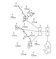
【0004】
一組のモバイルユニット10からの一組の逆方向リンク信号を処理するために形成された従来技術基地局の部分が図2に示される。運転中、アンテナシステム40は連合されたカバー領域にいるモバイルユニット10の組から同じRFバンドで伝送された一組の逆方向リンク信号を受信する。RF受信機42は逆方向リンク信号の組を下方変換およびデジタル化し、セルサイトモデム(CSM)44により受けられるデジタルサンプルを生じる。各CSM44は特定のモバイルユニット10からの特定の逆方向リンク信号を処理するため制御器46により割当てられ、各々BSC14へ転送されるデジタルデータを発生する。単一の集積回路で各CSMを実行するシステムおよび方法は、共に本発明の譲受人に譲渡され、ここに引用文献として組込まれた“スペクトラム拡散多元接続通信システムのセルサイト復調器アーキテクチュア”と題するU.S.特許No.5,654,979、および“スペクトラム拡散多元接続通信システムの多重経路探索処理装置” と題する継続中のU.S.出願シリアルNo.08/316,177に開示される。
【0005】
全般的に、基地局は典型的な都市名称のため十分な容量を提供するため、16および64間のモバイルユニットと同時にインターフェイスする容量でなくてはならない。これは各基地局12が16および64間のCSMを含むことを要求する。16および64間のCSMを使用している基地局は幅広い規模で実施されかつ配備されるので、かかる基地局のコストは比較的高い。このコストの主原因の1つはは、RFユニットからCSMへの相互接続、および基地局制御器およびCSM間の相互接続が複雑かつかなり敏感であることである。典型的に、24から3226のサブセットまたはそのようなCSMが回路板に置かれ、一組の回路板が背面を経て結合され、それは同軸ケーブル集団を使用してRFユニットへ結合される。かかる相互接続は高価でかなり信頼性に欠け、基地局12の全体のコスト、複雑性および保守に実質的に寄与する。それ故、かかる構成は非常に好ましくない。本発明はセルサイトモデムの大きな組を必要とすることなく、一組のモバイルユニットから受信される一組の逆方向リンク信号を処理するための方法および装置に向けられる。
【0006】
図3は発明の理解を容易にするために提供されたIS-95標準にしたがって、単一逆方向リンク通信量チャンネルを伝送するために使用された信号処理を示すブロック図である。伝送されたデータ48は、フレームと呼ばれる20msセグメント内に、それぞれ“フルレート”、“1/2レート”“1/4レート”“1/8レート”として参照される4つの伝送速度の1つで、各フレームは前と同量のデータの半分を含み、それ故レートの半分でデータを伝送するとして、たたみ込みエンコーダ50に供給される。データ48は、会話の中止中のような少ない情報が存在するとき、低いレートフレームが使用される典型的に可変レートのボコードされた音声情報である。回旋エンコーダ50はデータ48をたたみ込み的に符号化し、符号化された記号51を生じ、記号レピータ52はフルレートフレームに等価なデータの量を発生するため、足りる量により符号化された記号51を繰り返す記号により繰り返された記号53を発生する。例えば、1/4レートフレームの3つの付加的なコピーが4つのコピーの全体として発生されるが、フルレートフレームの付加的なコピーは発生されない。
【0007】
ブロックインターリーバ54はインターリーブされた記号55を発生するために繰り返された記号53をブロックインターリーブする。変調器56はウオルシュ記号57生じるためインターリーブされた記号55に64−アレイ変調を実行する。それは64の可能な直交ウオルシュコードの1つであり、64変調チップからなる各コードが6インターリーブされた記号55ごとに伝送される。データバーストランダマイザ58はデータのただ1つの完全な実例が伝送されるように、フレームレート情報を使用して、擬似ランダムでウオルシュ記号57をゲートすることを実行する。パワー制御命令が対応する期間ごとに基地局により発生されるので、ゲートは“パワー制御グループ”として引用された6ウオルシュ記号の増分で実行される。16パワー制御グループは、全ての16がフルレートフレームとして、8が1/2レートフレームとして、4が1/4レートフレームとして、2が1/8レートフレームとして伝送される状態で各20msフレームに対して起る。各低いレートフレームとして伝送されたパワー制御グループは高いレートフレームとして伝送されたグループのサブセットである。
【0008】
ゲートされたウオルシュチップは、4つの長いチャンネルコードのレートで擬似ランダム(PN)長いチャンネルコード59を使用して、各ウオルシュチップ発生変調データ61に直接シーケンス変調される。長いチャンネルコードは各モバイルユニット10に対して1つしかなく、各基地局によって知られている。変調されたデータ61は、I−チャンネルデータを生じる同相擬似ランダム拡散コード(PNI)で変調を経て“拡散”された第1コピーとして、および遅延60により拡散コードチップを1/2遅延され、Q−チャンネルデータを生じる直角位相擬似ランダム拡散コード(PNQ)で変調を経て拡散された第2コピーとして複写される。PNIおよびPNQ拡散データセットは、それぞれ同相および直角位相搬送信号に変調するために使用される前に、各々低域通過フィルタ(示されない)に通される。変調された同相および直角位相搬送信号は、基地局または他の受信システム(示されない)に伝送される前に合計される。
【0009】
発明の概要
本発明は同じRFバンドによって受信された多元信号のデジタル受信処理を実行する新規かつ改良されたシステムおよび方法である。発明の好ましい実施例において、デジタルRFサンプルが探索器および復調器によりアクセスされるRAM待ち行列に記憶される。探索器および復調器は好ましくはRAM待ち行列に沿って同じ集積回路に配置される。復調器はRAM待ち行列内に記憶された一組の逆方向リンク信号を復調し、各逆方向リンク信号は特定の時間オフセットで受信され、特定のチャンネルコードを使用して処理される。探索器は復調器により処理されない逆方向リンク信号、およびアクセスチャンネルを経て伝送されたアクセス要求について周期的に探索する。探索器は好ましくは、1/8レートフレームの間中に伝送される16パワー制御グループの2つに対応する各逆方向リンク信号の価値あるパワー制御グループの間中探索する。
【0010】
本発明の特徴、目的および利点は、同じ参照符号が対応している同一物を示す図面と共に理解されるとき以下に示す詳細な記述からより明らかになるであろう。
【0011】
好ましい実施例の詳細な記述
一組の信号を復調するシステムおよび方法が無線デジタルセルラー電話システムに関連して記述される。好ましい実施例において、受信デジタル処理は64ユーザまで実行でき、実質的に単一の集積回路を使用して実施される。かかる構成が好ましく、発明は特にかかる構成に適するが、発明はサテライトに基づいた通信システムおよび有線通信システム、およびデジタル信号処理が複数の集積回路を使用して実行されるシステムを含む他の構成にも採用され得る。
【0012】
図4は発明の一実施例により構成された受信処理システムのブロック図である。発明の好ましい実施例において、図4の受信処理システムはセルラー電話システムの基地局12内に配置される。示されるように、受信処理システムはアンテナシステム100に接続されたRF受信機102およびデジタル処理システム104を含む。デジタル処理システム104は好ましくは、ここに記述されるデジタルシステムの構成および作動により可能に作られた単一集積回路に配置される。デジタル処理システム104は好ましくはメモリ(示されない)に記憶されたソフトウエアを実行するマイクロプロセッサを含む外部制御システムで制御データを変換する。加えて、デジタル処理システム104はさらなる処理および最終目的地への配送のため図1の基地局制御器14へ伝送される受信データを発生する。また、多重RFユニットが例えば異なるアンテナまたは基地局のセクタに対応してデジタル処理システム104とインターフェイスしてもよい。
【0013】
運転中、受信機102はアンテナシステム100を経ていくらかのバックグランドノイズおよび干渉と共にモバイルユニットから一組の逆方向リンク信号を含むRFエネルギーを受信する。受信機102は濾波し、下方変換し、逆方向リンク信号の組を含むRFエネルギーの1.25MHzにデジタル化し、デジタル化されたサンプルをデジタル処理システム104へ供給する。好ましくは、デジタル化されたサンプルは略2.5MHzのサンプルレートのため、毎秒1.2288メガチップ(Mcps)である拡散チップレートで2回供給される。受信機102は技術においてよく知られている下方変換技術中、同相正弦(SIN)および直角位相正弦(COS)を混合することにより同相および直角位相サンプルを発生する。サンプルは好ましくは4ビットの分解能を有する。
【0014】
デジタル処理システム104内で、デジタルサンプルはアンテナインターフェイス(AI)循環バッファーRAM106に2xサンプルを記憶するRAMインターフェイス103により受けられる。循環バッファーRAM106はスタテックRAMを含むメモリシステムの任意の型であってもよい。一組の逆方向リンク信号および他のバックグランドノイズ内に特定の逆方向リンク信号を検出かつ追跡するに十分な受入れ可能な分解能を依然として提供している限り、デシメーションが循環バッファーRAMの必要な大きさを減少するために実行される。循環バッファーRAMは好ましくは任意の与えられた時間に同相および直角位相2xサンプルの両方の4つのウオルシュ記号価値を記憶し、それは2,048同相サンプルおよび2,048直角位相サンプルに対応する(4ウオルシュ記号*64ウオルシュチップ/記号*4拡散チップ/ウオルシュチップ*2サンプル/拡散チップ)。各サンプルが4ビットであるので、記述される実施例における必要な全メモリは2,048キロバイトである。
【0015】
制御システム110の制御のもと、および復調器PNコード発生器114からの擬似ランダムノイズコードの使用のもとで、復調器112は循環バッファーRAM106からのサンプルを受け、そこに記憶された一組の逆方向リンク信号を逆拡散する。上に注意したように、CDMA技術によれば、各逆方向リンク信号は各モバイルユニット10のため1つしかない一組のPNコードで変調および復調される。IS-95逆方向リンクについて、一組のPNコードは同相データの同相PNコード(PNI)、直角位相データの直角位相PNコード(PNQ)、および同相および直角位相信号の両方を変調するために使用されたユーザコード(PNU)を含む。復調された各逆方向リンク信号のPNコードの組の部分は復調器PNコード発生器114により供給される。
【0016】
IS-95標準にしたがって、変調中に使用されたPNコードの状態は、好ましくはGPS(全地球測位システム)受信機を使用し、パイロットチャンネルおよび同期チャンネルを経て各モバイルユニット10へ提供される、各基地局により知られかつ追跡されたシステム時間に依存する。モバイルユニット10は基地局から供給されるシステム時間に基づいたPNコードの組を使用して逆方向リンク信号を伝送する。基地局は、基地局におけるシステム時間に関して伝送遅れにより信号オフセットを処理するために使用される逆方向リンクPNコードの状態と調和して、いくらかの伝送遅れの後逆方向リンク信号を受信する。
【0017】
各オフセットは、それらが基地局12から異なる距離に配置されるので、各加入者ユニットについて全般的に異なる。逆方向リンク信号は、それらが発生されるモバイルユニット10のユーザコード(PNU)と同様にそれらのオフセットにより確認される。ユーザコードはモバイルIDまたはモバイルユニット10のESNから決定され得る。かくして、特定のモバイルユニット10から受信された信号は、モバイルユニット10 ESNおよび信号が受信されるオフセットを提供することにより参照され得る。同じモバイルユニット10からの信号の多重発生は典型的に反射および他の多重経路現象を経て発生され、経路は長さが異なる。好ましくは、復調器112は信号が検出されたオフセットで復調し、復調は通信が終了され、または信号がより長く検出されなくなるまで、これらのオフセットで連続して実行される。
【0018】
運転中、復調器112は制御システム110により特定されたオフセットで処理された各逆方向リンク信号のデータを出力する(“オンタイム”データのため“O”と呼ばれる)。加えて、復調器112は特定されたオフセットの前に拡散チップの1/2持続を処理された信号(早いため“E”と呼ばれる)、特定されたオフセットの後に拡散チップの1/2持続を処理された信号(遅いため“L”と呼ばれる)を出力する。発明の好ましい実施例において、同相および直角位相データの両方の偶数および奇数バージョンに対応している4つの出力を有して、4つの出力が各オフセットに関して発生される。偶数および奇数バージョンは、以下により詳細に記述される復調器FHTバンク116により処理を容易にするために提供される別々のバージョンを有して、受信されたデータの単に交互の部分である。
【0019】
復調器FHTバンク116は復調器112からオンタイム逆拡散データを受け、各々オンタイムソフト決定データを発生している同相および直角位相データの両方に速いハダマード変換(fast Hadamard transform)を実行する。早いおよび遅い復調データはタイムトラッキングシステム119へ供給され、それはオンタイム復調データがさらに処理される間にデータを記憶する。オンタイムソフト決定データはデインターリーバ118へ供給される。デインターリーバ118は20msブロックで各逆方向リンク信号として受信されたソフト決定データをデインターリーブし、デインターリーブされたソフト決定データはデコーダ120へ供給される。デコーダ120は好ましくは図1の基地局制御器へ転送されるハード決定データ122を生じるため、トレリス(trellis)またはビタービ(Viterbi)復号を実行する。
【0020】
タイムトラッキングシステム119は結合されたオンタイムソフト決定データと同様に早いおよび遅い逆拡散されたデータを受け、結合されたソフト決定データにより最も見こみがあると指示されたウオルシュ記号を使用している逆拡散されたデータをデカバーする。もしデカバーされた早いソフト決定データがより大きなエネルギーを含むなら、タイムトラッキングシステム119は、PNチップの小部分により処理された逆方向リンク信号の多重経路インスタンスで構成されたタイミングオフセット残余バッファー(フィンガー)をデクリメントインクリメント、即ち進める。特にタイミングオフセット残余バッファーは2エネルギーレベルの大きさの差に比例する量によりオフセットされる。もしデカバーされた遅いソフト決定データがより大きなエネルギーを含むなら、タイムトラッキングシステム119は、PNチップの同じ小部分により処理されたフィンガーで構成されたタイミングオフセット残余バッファーをインクリメントデクリメント、即ち遅らせる。
【0021】
処理が進められ、または遅らされることによりタイミングオフセットバッファーに記憶された量がPN拡散チップの1/8持続に達するとき、特定の逆方向リンク信号が処理される実際のオフセットはPN拡散チップの1/8持続により増加または減少される。発明の好ましい実施例において、タイミングオフセットバッファーが増加される量は、他の増加量の使用が本発明の使用と合致するが、復調された各16拡散チップについて拡散チップの1/204800の持続である。
【0022】
復調器112により実行された処理と同時に、探索器130は制御システム110の制御のもとで循環バッファーRAM106からのサンプルを検索する。特に、制御システム110は、循環バッファーRAM106に記憶されたサンプルの特定部分を検索し、もしそのモバイルからの逆方向リンク信号がその時間に受信されているなら、決定のため特定のモバイルユニット10の拡散コードの組を使用している一組の時間オフセット復調を実行することを探索器130に指示する。好ましくは、探索器130は新しい逆方向リンク信号を検出するため、逆方向リンク信号が復調器112により現在復調されなかった信号でないものについてオフセットで復調する。復調は好ましくは、ゼロオフセット変調(“0”と呼ばれる)、.5拡散チップオフセット(“.5” と呼ばれる)、1拡散チップオフセット(“1” と呼ばれる)、および1.5拡散チップオフセット(“1.5” と呼ばれる)に対応された4つの組で実行される。復調を実行するために使用されたPNコードは制御システム110の制御のもとで探索器PNコード発生器136により発生される。
【0023】
4つの復調の結果は、各復調の速いハダマード変換を実行する探索器FHTバンク132へ転送され、6ウオルシュ記号またはパワー制御グループによる結果を蓄積する。探索器FHTバンク132からのソフト決定エネルギーレベルの結果は探索器結果RAM134に記憶される。制御システム110は探索器結果RAM134にアクセスし、もしエネルギーレベルが種々の閾値以上で検出されるなら、構成された時間オフセットで処理を始めることを復調器112へ指示する。
【0024】
発明の一実施例によれば、デジタル処理システムは80の異なるモバイルユニット10までから発生されまたは伝送され得る256逆方向リンク信号を同時に処理するように構成される。加えて、特定逆方向リンク信号の6多重経路インスタンス(フィンガー)まで任意の与えられた時間に処理され得る。しかし、処理される逆方向リンク信号の全数が256を超えないので、任意の特定逆方向リンク信号の処理され得る多重経路インスタンスの数は、典型的に処理される逆方向リンク信号の全数、かつ各逆方向リンク信号の受信される多重経路インスタンスの数に依存して6より少ない。各逆方向リンク信号の6多重経路インスタンスまで一緒に処理されるように80の異なる逆方向リンク信号まで許容することは、システムが、高度に不規則な地形のために好まれる逆方向リンク信号のより小さな組の多くの多重経路インスタンスを処理するため、またはより規則的な地形のために好まれる多くの逆方向リンク信号のより少ない多重経路インスタンスを処理するために構成されてもよいという高められた柔軟性を提供する。
【0025】
加えて、80の異なる逆方向リンク信号の6例を処理する能力は、単一のデジタル処理システム104がセクタ毎に20モバイルユニット10を有する3セクタ基地局のために必要な信号処理を遂行することを許容する。セクタ毎に20モバイルユニットを有する3区分基地局は産業において共通の構成であり、それ故デジタル処理システム104は、非常に望ましい特に単一集積回路でかかる基地局12を実施することを可能にする。
【0026】
256信号の同時処理のため、デジタル処理システム104はPN拡散コードチップレート(チップx32)のそれの32回クロックレート、または略40MHzで作動する。このクロックレートで、復調器112は処理されている256信号の各々に32クロックサイクルを割当てることができる。同様に、探索器130は、それに各パワー制御グループ中検索される1024のスループットを与える操作毎に4つのオフセットの25632探索操作を実行できる。探索器130は受信された新PN拡散コードチップの各組のために32復調動作を実行する。加えて、各クロックサイクル中、探索器130は探索器PN拡散コード発生器136からの特定モバイルユニットの16PNコード拡散チップを受け、復調器112は復調器PN拡散コード発生器114からの特定モバイルユニットの16PNコード拡散チップを受ける。かくして、復調器112は64モバイルユニットからの受信された新拡散コードの各組のため、逆拡散復調器ごとに16PN拡散コードチップを各々含んでいる16の32逆拡散復調動作(逆拡散)(復調器)を実行する。探索器130はまた、4つのチップオフセット0、0.5、1.0、1.5の組で16PN拡散コードを各々含んでいる16の逆拡散された32復調器を実行する。
【0027】
PNコード発生器114および探索器PNコード発生器136は共にシステムPNコード発生器115からシステムコードを、およびマスクRAM117からMASK値を受ける。各ウオルシュ記号中、システムPNコード発生器115は、制御システム110の制御のもとで復調器PNコード発生器114および探索器PNコード発生器136の両方へシステムPNコードデータの72ビットを供給する。特に、システムPNコード発生器115は、種々の逆方向リンク信号が受信される時間オフセットに対応した種々の状態でシステムコードを発生する。かくして、復調器112は復調器PNコード発生器114により供給されたPNコードを使用して一組の逆方向リンク信号を復調し、探索器130は探索器PNコード発生器136により供給されたPNコードを使用して一組の逆方向リンク信号を復調する。
【0028】
図5は発明の一実施例により構成された復調器112のブロック図である。データレジスタ200は制御システム110の制御のもとで循環バッファーRAM106からのデジタルサンプルのブロックを検索する。制御システム110は、以下により詳細に記述されるように、その特定の時間に処理される逆方向リンク信号のオフセットに基づいて循環バッファーRAM内に検索されるべきデータのブロックを指定する。データ選択/マルチプレクサバンク(データ選択)202はデータをシフトすることにより制御システム110からのオフセット情報に基づいた2xデータサンプルの正確なオフセットを作り、時間オフセットデータをXORバンク204−210へ適用する。サンプルは同相および直角位相成分の両方の偶数および奇数部分に供給され、それ故4つの線が最も多い接続として示される。
【0029】
XORバンク204−210は同相および直角位相データの両方の偶数および奇数部分を処理するために4つのXORサブバンクを含む。各XORバンクはデカバーされたPNコードを受け、0.0チップオフセット逆拡散データ、0.5チップオフセット逆拡散データ、1.0チップオフセット逆拡散データおよび1.5チップオフセット逆拡散データを生じる互いから拡散チップの1/2持続のオフセットでサンプルにPNコードを適用する。PNコードは図4の復調器PNコード発生器114から受け、PNチップレジスタ215に記憶する。
【0030】
発明の好ましい実施例において、特定の逆方向リンク信号のPNコードが供給され、それから次の逆方向リンク信号のPNコードがPNチップレジスタ215にラッチされる前に、その逆方向リンク信号の4つのフィンガーの4つのオフセットまでの組が処理される。即ち、同じPNコードセグメントが循環バッファーRAM106からのサンプルの異なる組から選択された異なるインスタンスに対して特定の逆方向リンク信号の4つのインスタンスまで復調するために使用される。異なるサンプルが制御システム110からのオフセット情報に応答して復調器112により検索される。同じPNコードセグメントでの復調により、各フィンガーからの結果は以下に記述されるようにより容易に蓄積され得る。
【0031】
本発明は、信号情報の4つのウオルシュ記号が必要とされるまで記憶されるデスキュウ(deskew)バッファーとして循環バッファーRAM106を使用することにより、同じ逆方向リンク信号の異なるインスタンスを復調するために同じPNコードセグメントの使用を容易にする。サンプルの4つのウオルシュ記号価値を記憶することにより、逆方向リンク信号の同じ部分が各フィンガーの循環バッファーRAMに同時に記憶されることを可能にする。これは特定の逆方向リンク信号のフィンガーの結合中、付加的なメモリの使用の必要を除去する。発明の他の実施例は、遅れの導入のような同じ逆方向リンク信号の異なるフィンガーからのデータを一列に並べる代替例を使用してもよい。
【0032】
早い補間回路212は0.0チップオフセット逆拡散データおよび0.5チップオフセット逆拡散データを受け、補間に使用している最新オフセット(早い逆拡散データ)の前に、チップの持続の0、0.1251/8、0.251/4、または0.3753/8により逆拡散されたデータオフセットの値を計算する。特に、早い補間回路212はオンタイム補間回路214に対して0.5だけ逆拡散データオフセットした値を計算する。発明の代わりの実施例において、早い補間回路212は1.0および1.5チップオフセットデータも受けてもよい。発明の一実施例において、単純な直線補間が使用されるが、他の補間方法の使用も発明の作働と両立する。例えば、任意の7つのタップFIRが適当である。
【0033】
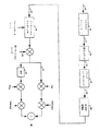
同様に、オンタイム補間回路214は0.5チップオフセット逆拡散データおよび1.0チップオフセット逆拡散データを受け、処理されるフィンガーの最新のオフセットに依存して、補間に使用している0.5−、0.6255/8、0.75−、または0.8757/8のオフセットでオンタイム逆拡散データの値を計算する。
【0034】
加えて、遅い補間回路216は1.0チップオフセット逆拡散データおよび1.5チップオフセット逆拡散データを受け、補間に使用している拡散チップ(遅い逆拡散データ)の持続1.01、1.1251 1/8、1.251 2/8または1.3751 3/8により遅延された逆拡散データの値を計算する。とくに、遅い補間回路216はオンタイム逆拡散データからの拡散チップ、および早い逆拡散データからの全部のチップの持続0.5遅延された逆拡散データを計算する。発明の一実施例において、直線補間がまた遅れた逆拡散データの値を計算するために使用される。例えば、15タップFIRが適する。早い、遅いおよびオンタイムデータは図4の復調器FHTバンク116に供給される。
【0035】
図6は発明の一実施例により構成された復調器FHTバンク116のブロック図である。32x2FHT300はオンタイム逆拡散データを受け、同相(I)および直角位相(Q)成分に速いハダマード変換を実行する。速いハダマード変換を実行するシステムおよび方法は本発明の譲受人に譲渡され、ここに引用文献として組込まれた“速いハダマード変換を実行するシステムおよび方法”と題するU.S.特許No.5,561,618に開示される。32x2FHT300の出力はI相関ベクトルおよびQ相関ベクトルを生じる偶数および奇数サンプルからの出力を結合する加算−減算バタフライ結合器308により処理される。I−Qドット積304は蓄積器306へ転送される相関エネルギーベクトルを生じるIおよびQ相関ベクトルのドット積を発生する。
【0036】
蓄積器306は同じ逆方向リンク信号の異なるインスタンス(フィンガー)に対応した一組の出力としてI−Qドット積304からのエネルギー相関ベクトルを蓄積する。一組のフィンガーの相関値の蓄積は、使用されるべき同じPNコードセグメントが循環バッファーRAM106内に記憶された同じ逆方向リンク信号の複数のインスタンスを復調することを許容する循環バッファーRAM内のサンプルの4つのウオルシュ記号価値の蓄積により容易にされる。
【0037】
特定の逆方向リンク信号からの全てのフィンガーからのエネルギー相関値が一度結合されたなら、蓄積されたエネルギー相関ベクトルは最大選択310へ供給され、それは伝送された最も見こみのある相関ベクトルから最大相関値を選択し、対応している索引値を発生する。最大検出操作を実行するシステムおよび方法は、本発明の譲受人に譲渡され、ここに引用文献として組込まれた“二重最大メトリック発生プロセスを採用している非コヒーレント受信機”と題するU.S.特許No.5,442,627に開示される。最大選択310の出力は図4のデインターリーバ118へ転送される。
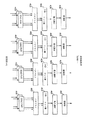
【0038】
図7は発明の一実施例により構成された探索器130のブロック図である。データレジスタ270が制御システム110の制御のもとで循環バッファーRAM106からのデジタルサンプルのブロックを受ける。制御システム110は、以下により詳細に記述されるように、その特定の時間に処理される逆方向リンク信号のオフセットに基づいた循環バッファーRAM内に検索されるべきデータのブロックを指定する。データ選択/マルチプレクサバンク(データ選択)272は制御システム110からのオフセット情報に基づいた処理されるデータの時間オフセットを調節し、時間オフセットデータをXORバンク274−280へ適用する。サンプルは同相および直角位相成分の両方の偶数および奇数部分に供給され、それ故4つの線が最も多い接続として示される。
【0039】
XORバンク274−280は同相および直角位相データの両方の偶数および奇数部分を処理するため、それぞれ4つのXORサブバンクを含む。各XORバンクは復調されたPNコードを受け、0.0チップオフセット逆拡散データ、0.5チップオフセット逆拡散データ、1.0チップオフセット逆拡散データおよび1.5チップオフセット逆拡散データを生じる互いから拡散チップの1/2持続のオフセットでサンプルにPNコードを適用する。PNコードは図4の探索器PNコード発生器114から受けられ、PNチップレジスタ295に記憶される。4つのオフセットのチップオフセット逆拡散データは探索器FHTバンクへ転送される。
【0040】
図8は発明の一実施例により構成された探索器FHTバンク132のブロック図である。処理される各オフセットについて、32x2FHT対400が早い逆拡散されたデータを受け、同相(I)および直角位相(Q)成分の早いハダマード変換を実行する。32x2FHT対400の出力は、交互の加算−減算方法でI相関ベクトルおよびQ相関ベクトルを生じる、偶数および奇数サンプルからの出力を結合する加算−減算バタフライ結合器402により処理される。I−Qドット積404は、各オフセットについて一組の相関エネルギーベクトルを生じるIおよびQ相関ベクトルのドット積を発生する。
【0041】
最大選択回路406は各エネルギー相関ベクトルから最大エネルギー相関ベクトルを選択し、蓄積器408が一組のウオルシュ記号によるエネルギー相関値を蓄積する。好ましくは、蓄積器408はパワー制御グループに対応する一組の6つのウオルシュ記号のエネルギー相関値を蓄積する。6つのウオルシュ記号の使用は十分に高い可能性で逆方向リンク信号を検出するため十分なエネルギーを蓄積することを許容し、また受信された十分な逆方向リンク信号を適切に検出するため十分な数の検索が実行されることを許容する。蓄積器410の出力は探索器結果RAM134へ転送される。
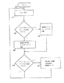
【0042】
復調プロセスに戻ると、図9は発明の一実施例により復調器FHTバンク116(図4)内でオンタイム復調の蓄積フェイズ中に実行されるステップのフローダイアグラムである。処理はステップ450で始まり、ステップ451でFHTからのエネルギー相関値のベクトルが受信される。ステップ452で、入来エネルギーベクトルが特定のモバイルユニット10から最初に受信されたか否かが決定される。もしそうなら、蓄積器306(図6)がクリアされ、ベクトルが今クリアされた蓄積器に記憶される。もしそうでないなら、ステップ455でエネルギーベクトルが蓄積器306に現に記憶されたエネルギーベクトルに加算される。ステップ458において、ベクトルが特定のモバイルユニット10からの最期のベクトルとして処理されたか否かがさらに決定される。もしそうでないなら、ステップ451が再び実行される。もしそうなら、蓄積器に記憶された値はステップ456で最大検出回路に転送され、ステップ451が再び実行される。
【0043】
図10は発明の一実施例により構成された復調器PNコード発生器114のブロック図である。同相拡散コード(PNI)カスケード発生器600、直角位相拡散コード(PNQ)カスケード発生器602およびユーザコードカスケード発生器604が各々制御システム110からスタート状態情報を受ける。スタート状態情報は好ましくはIS-95標準における使用で、42ビット数の形を与えられる特定の逆方向リンクを処理するシステム時間である。スタート状態は256拡散チップ毎に一度、またはウオルシュ記号ごとに一度好ましく供給される。
【0044】
スタート状態の使用で、カスケード発生器600および602は各々クロックサイクル毎に8拡散コードチップを発生する。加えて、カスケード発生器604は、スタート状態およびユーザマスクRAM117からの対応しているユーザマスクを使用してクロックサイクル毎に8ビットのユーザコードを発生する。ユーザコードは同相および直角位相拡散コードでXORされ、結果としての結合されたコードは復調器112へ転送される。
【0045】
探索器PNコード発生器136は、スタート状態および使用されるマスクコードが復調される逆方向リンク信号と同じである必要性のない任意の与えられた時間について、探索される特定の逆方向リンク信号として異なることを除いて、復調器PNコード発生器114と似た方法で作動する。
【0046】
図11は発明の一実施例により構成されたユーザコードカスケード発生器604のブロック図である。状態1レジスタ700は制御システム110からのスタート状態を受け、論理回路710にそれを適用する。論理回路710はIS-95標準にしたがって次の状態を発生するために必要な演算をし、かくしてシステムコードの状態が1つの拡散チップだけ進められ、それは状態2レジスタ702に記憶される。IS-95標準にしたがって実質的にデータをフォーマットするシステムおよび方法は、本発明の譲受人に譲渡され、ここに引用文献として組込まれた“伝送のためのデータをフォーマットする方法および装置”と題するU.S.特許No.5,504,773に開示される。
【0047】
論理回路712−716および状態レジスタ704−708は同様に計算しかつ前の状態レジスタに関して1つ拡散コードチップだけ進められたシステム時間を記憶し、論理回路716の出力は状態1レジスタ700の入力へ適用される。かくして、一度8つの状態が計算されると、次の8つの状態は論理回路716の出力を状態1レジスタ700にラッチすることにより計算され得る。レジスタのより少ないまたはより多い数を計算するカスケード発生器が使用されてもよい。加えて拡散コードはより速いクロックレートを使用して計算されてもよいが、カスケード発生器の使用はそれが電力消費を減少するようにするのが好ましい。技術に熟練した者は拡散コードを計算する代わりの方法を認識するであろう。
【0048】
状態レジスタ700−708の出力はまた、復調されたモバイルユニット10に対応しているユーザマスクRAMからのユーザマスク720とANDされ、XORされ、結果としての数は1ビットにXORされる。結果として8つのビットが8ビットユーザコードセグメント722を形成する。8ビットユーザコードセグメント722は上述されたように同相および直角位相拡散コードで付加的にXORしている出力である。同相および直角位相拡散コードカスケード発生器600および602はユーザコードカスケード発生器604と似た方法で作動するが、ユーザコードマスクおよびIS-95標準により特定されたようなユーザの異なる大きさの状態レジスタおよび異なる論理回路を使用しない。
【0049】
図12は発明の一実施例により構成された循環バッファーRAM待ち行列の実際上の構造図である。待ち行列は環状配列に構成され、それにより最新のサンプルが最も古いサンプルの上に書かれる。待ち行列の容量はIおよびQデジタルサンプルマスク1WS−4WS両方の4ウオルシュ記号を記憶するに十分である。最新のサンプルは線498Aで始まり、線498B−498Dはそれぞれサンプルの1つのウオルシュ記号価値を区画する。他の逆方向リンク信号は、その逆方向リンク信号の特定の到達時間に依存して異なる時間オフセットで起るこれらの逆方向リンク信号のウオルシュ記号境界とともに、データの4つのウオルシュ記号価値内に記憶される。例えば、線500は第1逆方向リンク信号のウオルシュ記号境界を区画し、線502は第2逆方向リンク信号のウオルシュ記号境界を区画する。
【0050】
見やすいように、ある逆方向リンク信号のあるウオルシュ記号は循環バッファーRAM待ち行列内に完全には記憶されない。部分的に記憶されたウオルシュ記号は正確に復調されない。しかし、サンプルの4つのウオルシュ記号価値を記憶することは、サンプルの少なくとも2つの完全なウオルシュ記号が各逆方向リンク信号のために記憶されることを確実にする。しばしばあるインスタンスにおいて、3つのウオルシュ記号が情報ルートを経て循環バッファーRAMにより復調されかもしれず、それによりウオルシュ記号のスタートはそれが書かれる前にちょうど復調される。
【0051】
2つの完全なウオルシュ記号は、カバー領域の縁からの伝送、および次から基地局への伝送間からこうむられたオフセットの多分最大差に対応する。2つの完全なウオルシュ記号はまた、特定の逆方向リンク信号の直接経路伝送および全般的に引き受けられたセルサイズのその逆方向リンク信号の他の反射された多重経路成分間の多分最大オフセットに対応する。かくして、同じシステム時間で伝送された逆方向リンク信号は、たとえそれらが基地局のカバー領域内で異なる位置から伝送されたとしても、異なるメモリ位置であるけれども循環バッファーRAM内に同時に記憶されるであろう。循環バッファーRAMの大きさを増大することにより、より大きなセルサイズが適応され得る。加えて、6ウオルシュ記号循環バッファーRAMの使用は、典型的にある程度の回帰的復調および、そのためより多い処理時間を必要とするコヒーレント復調を実行するために有用である。8ウオルシュ記号循環バッファーRAMの使用は、知られたデータの探索およびまた回帰的処理を含む補助されたデータ、または因果関係のない復調のために有用である。
【0052】
再び図4を参照すると、運転中制御システム110は循環バッファーRAMに記憶された最も近いサンプルの基地局におけるシステム時間を追跡する。加えて、制御システム110は、現に知られかつ復調器112により処理されている各逆方向リンク信号のオフセット即ち遅れを追跡する。オフセットを使用して、制御システム110は各逆方向リンク信号の処理されるべきサンプルの次の組の循環バッファーRAM内のメモリアドレス位置を計算し、そのスタートアドレスを復調器112へ供給する。加えて、制御システム110はPNコードを発生させるため、逆方向リンク信号の組を復調器PNコード発生器に提供する。復調器112は特定されたオフセットで循環バッファーRAMからメモリを検索し、復調器PN拡散コード発生器114からのPN拡散コードを図5のデータ選択202を使用している特定オフセットに適用する。
【0053】
同様に、制御システム110は探索する逆方向リンク信号およびオフセットが何かを計算する。計算は好ましくは内部探索アルゴリズムに応答しており、特定のモバイルユニット10がその基地局のカバー領域に入っていることを基地局に通知している図1の基地局制御器14から受信された制御データに応答する。この通知は発生されるべきPNコードを許容するモバイルユニットについて確認情報を含む。
【0054】
制御システム110はメモリアドレス位置を計算し、これらのメモリアドレス位置を探索器130に供給する。加えて、制御システムはPNコードを発生させるため、ユーザのアイデンティティを探索器PNコード発生器136に供給する。サンプルの各新しい拡散チップ価値が受けられるので、探索器は制御システム110からの特定アドレス位置で始め、または続ける循環バッファーRAMからのサンプルを検索し、検索器PNコード発生器136からのPNコードを適用する。
【0055】
発明の一実施例において、制御システム110は任意の与えられた時間に探索する逆方向リンク信号を計算するとき2つの要因を考慮するが、付加的な要因がまた考慮されてもよい。第1に、もし特定の逆方向リンク信号のパワー制御グループが“価値ある”グループにあるなら、制御システム110が決定する。即ち、制御システム110は、現パワー制御グループが1/8レートフレームとして伝送されているか否かを決定する。もしそうなら、たとえ選ばれたモバイルのレートが何であるとしても、逆方向リンク信号がこの時に伝送されかつ受信されていることが保証され得、それ故検出のために利用可能である。発明の好ましい実施例において、価値あるパワー制御グループはIS-95標準に示された予定のアルゴリズムに基づいて基地局に知られる。加えて、実質的にIS-95標準によるデータ伝送のシステムおよび方法は、本発明の譲受人に譲渡され、ここに引用文献として組込まれた“データバーストランダマイザ”と題するU.S.特許No.5,659,569に開示される。
【0056】
価値あるパワー制御グループを現に伝送しているこれらのモバイルユニットのため、制御システム110は、探索が導入されることなく逆方向リンク信号が時間の最長期間過ぎたことを決定する。制御システム110はさらに、探索器130の与えられた容量を実行され得る探索器の数を決定し、利用可能な容量まで探索することなく最長を過ぎた逆方向リンク信号の組だけのために探索を要求する。加えて、制御システム110は、各パワー制御グループ中、探索がアクセスチャンネル伝送のため実行されることを要求し、その上通信がなされるよう開始することを要求する。アクセスチャンネルは、ユーザマスクで発生された個人的なユーザコード(PNU)よりはむしろ、全てのモバイルユニット10について同じである公共の知られたアクセスの長いコードで発生された単純な正常の逆方向リンク信号である。
【0057】
図13は発明の一実施例により探索中に実行されるステップのフローダイアグラムである。探索はステップ250で始まり、ステップ252で価値あるパワー制御グループ中に受信されたモバイルユニット10が価値ある信号として確認される。ステップ254で、最期の探索がその信号のために実行された以来の時間により価値ある信号がランク付けされ、ステップ256で、最期の探索以来最長時間が経過した一組の価値ある信号について、探索器の最大容量にまで探索が要求される。一度探索が要求されると、各逆方向リンク信号のために実行された最期の探索以来の時間が更新され、探索はステップ258で終了する。発明の好ましい実施例において、探索は正常な運転中前進方法で繰返し実行される。
【0058】
図14は発明の一実施例により構成されたタイムトラッキングユニット119のブロック図である。遅延/デマルチプレクサFIFO550は復調器112から早いおよび遅い逆拡散データを受け、同じ逆方向リンク信号の6つの異なる発生(フィンガー)まで、遅延/デマルチプレクサFIFO550内のレジスタF1−F6へ記憶する。もし6多重経路より少ない経路が復調されているなら、全てのレジスタF1−F6はデータを含まないであろう。早いおよび遅い両データの偶数および奇数部分が各フィンガーの単一データストリームにデマルチプレクスされ、デマルチプレクスされたデータストリームがデカバー回路552に供給される。デカバー回路552はまた選択されたウオルシュ記号のウオルシュ索引を受ける。
【0059】
ウオルシュ索引の使用が利用可能になるとき、デカバー回路552は、ウオルシュ索引に対応するウオルシュ記号でデータを含むこれらのレジスタF1−F6に記憶された早いおよび遅い逆拡散されたデータを直列方法でデカバー、即ち復調することを始め、各フィンガーの同相および直角位相の早いおよび遅い復調データを生じる。各フィンガーの同相および直角位相の早いおよび遅い復調データは、同相および直角位相データの計算ドット積の大きさを発生するI−Qドット積回路554に供給され、各フィンガーの早いおよび遅いエネルギー値を生じる。比較回路558は各フィンガーの早いおよび遅い処理が最強のエネルギーレベルを作り出すか否かを指示し、その指示を制御システム110へ転送する。
【0060】
制御システム110は構成されたフィンガーのオフセットによりバッファーに存するタイムトラッキングを増加または減少することにより比較回路558からの指示データに応答し、それ故各復調動作の拡散コードチップの1/2,000の持続に貢献し、構成されたフィンガーの処理を進めまたは遅らせる。タイムトラッキングバッファーが上述のように拡散チップの1/8持続により変化するとき、明らかなように、各フィンガーのオフセットが独立に変化するので、フィンガーは別々に処理される。しかし、オンタイム相関ベクトルが結合され得る間各フィンガーの処理を遅らせることにより、最も見こみのあるウオルシュ記号が全てのフィンガーからのエネルギーを使用して選択され得、かくして正確な選択の見込みを増加する。
【0061】
かくして、単一または減少された数の集積回路で実施され得る、複数の信号、好ましくはCDMA信号の処理システムおよび方法が記述された。好ましい実施例の先の記述は、技術に熟練した者ならだれでも本発明を作りまたは使用することを可能にするように提供された。これらの実施例に対する種々の変形例がすでに技術に熟練した者に明らかであり、ここに定義された基本的原理は発明能力を使用することなく他の実施例に適用されるかもしれない。かくして、本発明はここに示された実施例に限定されることを意図されず、ここに開示された原理および新規な特長を構成する最も広い範囲に従わされるべきである。
【図面の簡単な説明】
【図1】 セルラー電話システムのブロック図である。
【図2】 従来技術により形成された基地局の部分のブロック図である。
【図3】 IS-95逆方向リンク信号を発生するために使用される伝送システムのブロック図である。
【図4】 発明の一実施例により形成された基地局の受信処理システムの部分のブロック図である。
【図5】 発明の一実施例により形成された復調器のブロック図である。
【図6】 発明の一実施例により形成された復調器FHTバンクのブロック図である。
【図7】 発明の一実施例により形成された探索器のブロック図である。
【図8】 発明の一実施例により形成された探索器FHTバンクのブロック図である。
【図9】 発明の一実施例により実行されるオンタイム復調の累積位相中に実行されるステップのフローチャートである。
【図10】 発明の一実施例により形成された復調器PNコード発生器のブロック図である。
【図11】 発明の一実施例により形成されたPNコードカスケード発生器のブロック図である。
【図12】 発明の一実施例により形成されたアンテナインターフェイスRAM待ち行列の構造のブロック図である。
【図13】 発明の一実施例により実行される探索中に実行されるステップのフローチャートである。
【図14】 発明の一実施例により形成されたタイムトラッキングユニットのブロック図である。
【符号の説明】
10…モバイルユニット、12…基地局、14…基地局制御器、16…モバイル交換センター、40…アンテナシステム、42…受信機、44…セルサイトモデム、46…制御器、50…たたみ込みエンコーダ、52…記号レピータ、54…ブロックインターリーバ、56…変調器、58…データバーストランダマイザ、100…アンテナシステム、102…受信機、103…インターフェイス、104…デジタル処理システム、110…制御システム、112…復調器、114…復調器PNコード発生器、115…システムPNコード発生器、116…復調器FHTバンク、118…デインターリーバ、119…タイムトラッキングシステム、120…デコーダ、130…探索器、132…探索器FHTバンク、136…探索器PNコード発生器、200、270…データレジスタ、202、272…データ選択/マルチプレクサバンク、204…バンク、212…早い補間回路、214…オンタイム補間回路、215…PNチップレジスタ、216…遅い補間回路、274…バンク、304…I-Qドット積、306…蓄積器、308…算バタフライ結合器、310…最大選択、402…バタフライ結合器、404…I-Qドット積、406…最大選択回路、408…蓄積器、552…デカバー回路、554…I-Qドット積回路、558…比較回路、600…同相拡散コードカスケード発生器、602…直角位相拡散コードカスケード発生器、604…ユーザコードカスケード発生器、700、702、…708…レジスタ、710、712、…716…論理回路[0001]
Background of the Invention
I. Field of Invention
The present invention relates to digital wireless communications. More particularly, the present invention relates to a new and improved demodulator for processing a series of user signals that facilitates means for implementing a signal integrated circuit.
II. Description of related technology
FIG. 1 is a block diagram of a highly simplified cellular telephone formed through the use of a code division multiple access (CDMA) over-the-air interface. In particular, FIG. 1 shows a cellular telephone system formed through the use of the IS-95 standard, which uses CDMA signal processing techniques that provide a highly efficient and robust cellular telephone service. IS-95, and its derivations such as IS-95A and ANSI J-STD-008 (collectively referred to here as IS-95), as well as other well-known standards bodies, Distributed by the industrial association (TIA). In addition, a cellular telephone system substantially formed by the use of IS-95 is assigned to the assignee of the present invention and is incorporated herein by reference as a system for generating signal waveforms in a CDMA cellular telephone system and US patent no. 5,103,459.
[0002]
The first advantage of using a CDMA over the air interface is that communications are carried over the same RF band. For example, each mobile unit 10 (typical cellular phone) shown in FIG. 1 can communicate with the
[0003]
During typical operation of the cellular telephone system of FIG. 1, the
[0004]
A portion of a prior art base station formed to process a set of reverse link signals from a set of
[0005]
Overall, the base station must be capable of interfacing between 16 and 64 mobile units simultaneously to provide sufficient capacity for typical city names. This requires that each
[0006]
FIG. 3 is a block diagram illustrating the signal processing used to transmit a single reverse link traffic channel in accordance with the IS-95 standard provided to facilitate understanding of the invention. Each transmitted
[0007]
[0008]
The gated Walsh chip has four long channel codes rate The pseudo-random (PN)
[0009]
Summary of the Invention
The present invention is a new and improved system and method for performing digital reception processing of multiple signals received over the same RF band. In the preferred embodiment of the invention, digital RF samples are stored in a RAM queue accessed by the searcher and demodulator. The searcher and demodulator are preferably located on the same integrated circuit along a RAM queue. The demodulator demodulates a set of reverse link signals stored in the RAM queue, each reverse link signal being received at a specific time offset and processed using a specific channel code. The searcher periodically searches for reverse link signals that are not processed by the demodulator and access requests transmitted via the access channel. The searcher is preferably 1/8 rate Search throughout the valuable power control group of each reverse link signal corresponding to two of the 16 power control groups transmitted during the frame.
[0010]
The features, objects and advantages of the present invention will become more apparent from the detailed description set forth below when taken in conjunction with the drawings in which like reference characters indicate corresponding parts.
[0011]
Detailed Description of the Preferred Embodiment
A system and method for demodulating a set of signals is described in the context of a wireless digital cellular telephone system. In the preferred embodiment, the received digital processing can be performed up to 64 users and is implemented using a substantially single integrated circuit. Such a configuration is preferred and the invention is particularly suitable for such a configuration, but the invention applies to other configurations including satellite-based communication systems and wired communication systems, and systems where digital signal processing is performed using multiple integrated circuits Can also be employed.
[0012]
FIG. 4 is a block diagram of a reception processing system configured according to one embodiment of the invention. In the preferred embodiment of the invention, the reception processing system of FIG. 4 is located in the
[0013]
During operation, the
[0014]
Within the
[0015]
Under the control of the
[0016]
According to the IS-95 standard, the state of the PN code used during modulation is preferably provided to each
[0017]
Each offset is generally different for each subscriber unit because they are located at different distances from the
[0018]
During operation,
[0019]
[0020]
[0021]
When the amount stored in the timing offset buffer reaches one-eighth duration of the PN spreading chip as processing is advanced or delayed, the actual offset at which a particular reverse link signal is processed is the PN spreading chip Increased or decreased by 1/8 of the duration. In the preferred embodiment of the invention, the amount by which the timing offset buffer is increased is the duration of 1/204800 of the spread chip for each 16 spread chips demodulated, although the use of other increase amounts is consistent with the use of the present invention. is there.
[0022]
Simultaneously with the processing performed by
[0023]
The results of the four demodulations are transferred to a
[0024]
According to one embodiment of the invention, the digital processing system is configured to simultaneously process 256 reverse link signals that can be generated or transmitted from up to 80 different
[0025]
In addition, the ability to process 6 instances of 80 different reverse link signals, the single
[0026]
For simultaneous processing of 256 signals,
[0027]
Both the PN code generator 114 and the searcher
[0028]
FIG. 5 is a block diagram of
[0029]
XOR banks 204-210 In phase and Quadrature Four XOR subbanks are included to handle both even and odd portions of the data. Each XOR bank Decover 0.0 chip offset with the received PN code Reverse diffusion Data, 0.5 chip offset Reverse diffusion Data, 1.0 chip offset Reverse diffusion Data and 1.5 chip offset Reverse diffusion Apply a PN code to the samples with a 1/2 duration offset of the spreading chip from each other that produces the data. The PN code is received from the demodulator PN code generator 114 shown in FIG. 4 and stored in the PN chip register 215.
[0030]
In the preferred embodiment of the invention, the PN code of a particular reverse link signal is provided, and then the four PN codes of that reverse link signal are latched into the PN chip register 215 before the next PN code is latched into the PN chip register 215. Groups of up to four offsets of fingers are processed. That is, the same PN code segment is different selected from different sets of samples from the
[0031]
The present invention differs from the same reverse link signal by using the
[0032]
[0033]
Similarly, the on-
[0034]
In addition, the
[0035]
FIG. 6 is a block diagram of
[0036]
[0037]
Once the energy correlation values from all fingers from a particular reverse link signal are combined once, the accumulated energy correlation vector is fed to max selection 310, which is the maximum from the most likely transmitted correlation vector. Select a correlation value and generate a corresponding index value. A system and method for performing a maximum detection operation is assigned to the assignee of the present invention and is hereby incorporated by reference into the US Patent No. entitled “Non-Coherent Receiver Employing Dual Maximum Metric Generation Process”. . 5,442,627. The output of the maximum selection 310 is shown in FIG. Deinterleaver Forwarded to 118.
[0038]
FIG. 7 is a block diagram of
[0039]
XOR banks 274-280 In phase and Quadrature In order to process both the even and odd portions of the data, each includes four XOR subbanks. Each XOR bank receives a demodulated PN code and has a 0.0 chip offset Reverse diffusion Data, 0.5 chip offset Reverse diffusion Data, 1.0 chip offset Reverse diffusion Data and 1.5 chip offset Reverse diffusion Apply a PN code to the samples with a 1/2 duration offset of the spreading chip from each other that produces the data. The PN code is received from the searcher PN code generator 114 of FIG. 4 and stored in the
[0040]
FIG. 8 is a block diagram of
[0041]
A
[0042]
Returning to the demodulation process, FIG. 9 is a flow diagram of the steps performed during the accumulation phase of on-time demodulation within the demodulator FHT bank 116 (FIG. 4) according to one embodiment of the invention. Processing begins at
[0043]
FIG. 10 is a block diagram of demodulator PN code generator 114 constructed in accordance with one embodiment of the invention. In phase Spread code (PNI)
[0044]
Using the start state,
[0045]
Searcher
[0046]
FIG. 11 is a block diagram of a user
[0047]
Logic circuits 712-716 and status registers 704-708 similarly calculate and store the system time advanced by one spreading code chip with respect to the previous status register, and the output of
[0048]
The outputs of the status registers 700-708 are also ANDed with the
[0049]
FIG. 12 is a practical structural diagram of a circular buffer RAM queue constructed in accordance with one embodiment of the invention. The queue is organized in a circular arrangement so that the latest sample is written over the oldest sample. The queue capacity is sufficient to store the 4 Walsh symbols of both the I and Q digital sample masks 1WS-4WS. The latest sample begins at
[0050]
For clarity, certain Walsh symbols with certain reverse link signals are not completely stored in the circular buffer RAM queue. Partially stored Walsh symbols are not demodulated correctly. However, storing the four Walsh symbol values of the sample ensures that at least two complete Walsh symbols of the sample are stored for each reverse link signal. Often instance At three Walsh symbols may be demodulated by the circular buffer RAM via the information route, so that the start of the Walsh symbol is just demodulated before it is written.
[0051]
Two complete Walsh symbols correspond to possibly the maximum difference in offset from the transmission from the edge of the coverage area and from the next transmission to the base station. Two complete Walsh symbols also correspond to the most likely offset between the direct path transmission of a particular reverse link signal and other reflected multipath components of that reverse link signal of generally assumed cell size To do. Thus, reverse link signals transmitted in the same system time are stored at the same time in the circular buffer RAM even though they are transmitted from different locations within the coverage area of the base station, even though they are at different memory locations. I will. Larger cell sizes can be accommodated by increasing the size of the circular buffer RAM. In addition, the use of a 6 Walsh symbol circular buffer RAM is useful for performing coherent demodulation that typically requires some degree of recursive demodulation and therefore more processing time. The use of an 8 Walsh symbol circular buffer RAM is useful for assisting data including known data searching and also recursive processing, or for non-causal demodulation.
[0052]
Referring again to FIG. 4, the
[0053]
Similarly, the
[0054]
[0055]
In one embodiment of the invention, the
[0056]
For those mobile units that are currently transmitting a valuable power control group, the
[0057]
FIG. 13 is a flow diagram of the steps performed during a search according to one embodiment of the invention. The search begins at
[0058]
FIG. 14 is a block diagram of a
[0059]
When the use of the Walsh index becomes available,
[0060]
The
[0061]
Thus, a system and method for processing multiple signals, preferably CDMA signals, that can be implemented on a single or reduced number of integrated circuits has been described. The previous description of the preferred embodiments has been provided to enable any person skilled in the art to make or use the present invention. Various modifications to these embodiments will be apparent to those skilled in the art, and the basic principles defined herein may be applied to other embodiments without using inventive capabilities. Thus, the present invention is not intended to be limited to the embodiments shown herein, but is to be accorded the widest scope constituting the principles and novel features disclosed herein.
[Brief description of the drawings]
FIG. 1 is a block diagram of a cellular telephone system.
FIG. 2 is a block diagram of a portion of a base station formed according to the prior art.
FIG. 3 is a block diagram of a transmission system used to generate IS-95 reverse link signals.
FIG. 4 is a block diagram of portions of a base station reception processing system formed in accordance with one embodiment of the invention.
FIG. 5 is a block diagram of a demodulator formed in accordance with an embodiment of the invention.
FIG. 6 is a block diagram of a demodulator FHT bank formed in accordance with one embodiment of the invention.
FIG. 7 is a block diagram of a searcher formed in accordance with one embodiment of the invention.
FIG. 8 is a block diagram of a searcher FHT bank formed in accordance with one embodiment of the invention.
FIG. 9 is a flowchart of steps performed during the cumulative phase of on-time demodulation performed in accordance with one embodiment of the invention.
FIG. 10 is a block diagram of a demodulator PN code generator formed in accordance with one embodiment of the invention.
FIG. 11 is a block diagram of a PN code cascade generator formed in accordance with one embodiment of the invention.
FIG. 12 is a block diagram of the structure of an antenna interface RAM queue formed in accordance with one embodiment of the invention.
FIG. 13 is a flowchart of steps performed during a search performed in accordance with one embodiment of the invention.
FIG. 14 is a block diagram of a time tracking unit formed in accordance with an embodiment of the invention.
[Explanation of symbols]
10 ... Mobile unit, 12 ... Base station, 14 ... Base station controller, 16 ... Mobile switching center, 40 ... Antenna system, 42 ... Receiver, 44 ... Cell site modem, 46 ... Controller, 50 ... Convolution Encoder, 52 ... Symbol repeater, 54 ... Block interleaver, 56 ... Modulator, 58 ... Data burst randomizer, 100 ... Antenna system, 102 ... Receiver, 103 ... Interface, 104 ... Digital processing system, 110 ... Control system, 112 ... demodulator, 114 ... demodulator PN code generator, 115 ... system PN code generator, 116 ... demodulator FHT bank, 118 ... Deinterleaver 119:
Claims (14)
前記デジタルサンプルを第1の組のタイムオフセットで復調する探索器と、
前記デジタルサンプルを第2の組のタイムオフセットで復調する復調器と、
前記第1の組のタイムオフセットと前記第2の組のタイムオフセットとを特定する制御システムとを含み、前記探索器がさらに前記アンテナ入力メモリからの第1の組のデジタルサンプルを検索し、前記第1の組のタイムオフセットからのタイムオフセットに適用された第1のPNコードで前記第1の組のデジタルサンプルを復調する、
各信号が1つまたはそれ以上の多重経路インスタンスを有する一組のCDMA信号を復調するシステム。An antenna input memory for storing digital samples of radio frequency energy;
A searcher for demodulating the digital samples with a first set of time offsets;
A demodulator that demodulates the digital samples with a second set of time offsets;
A control system that identifies the first set of time offsets and the second set of time offsets, wherein the searcher further retrieves the first set of digital samples from the antenna input memory, and demodulating the digital samples of the first set with a first PN code applied to a time offset from the first set of time offsets,
A system that demodulates a set of CDMA signals, each signal having one or more multipath instances.
前記アンテナ入力メモリからの第2の組のデジタルサンプルを検索し、
前記第2の組のデジタルサンプルを前記第2の組のタイムオフセットからのタイムオフセットに適用された第2のPNコードで復調する請求項1に示すシステム。The demodulator further comprises:
Retrieving a second set of digital samples from the antenna input memory;
The system shown in claim 1 for demodulating the digital samples of the second set with a second PN code applied to a time offset from the second set of time offsets.
前記探索器は前記復調器によって復調されなかった信号を復調する請求項1に示すシステム。The demodulator demodulates an already detected signal;
The system of claim 1, wherein the searcher demodulates a signal that was not demodulated by the demodulator.
前記第2の組のタイムオフセットで前記デジタルサンプルを復調するため第2の組のPNコードを発生する復調器PNコード発生器とをさらに含んでいる請求項1のシステム。A searcher PN code generator for generating a first set of PN codes to demodulate the digital samples at the first set of time offsets;
The system of claim 1, further comprising a demodulator PN code generator that generates a second set of PN codes to demodulate the digital samples at the second set of time offsets.
前記アンテナ入力メモリから探索器により第1の組のサンプルを検索し、
前記デジタルサンプルを前記探索器により第1の組のタイムオフセットで復調し、
前記デジタルサンプルを復調器により第2の組のタイムオフセットで復調し、
前記第1の組のデジタルサンプルを前記第1の組のタイムオフセットからのタイムオフセットに適用された第1のPNコードで前記探索器により復調するステップを含み、
各信号が1つまたはそれ以上の多重経路インスタンスを有する一組のCDMA信号を復調する方法。Store digital samples of radio frequency energy in the antenna input memory,
Search the first set of samples by a searcher from the antenna input memory,
Demodulating the digital samples with the searcher with a first set of time offsets;
Demodulating the digital samples with a second set of time offsets by a demodulator;
Wherein the step of demodulating by said searcher at the first PN code applied to the digital samples of the first set to the time offset from the first set of time offsets,
A method of demodulating a set of CDMA signals, each signal having one or more multipath instances.
前記復調器は前記第2の組のデジタルサンプルを前記第2の組のタイムオフセットからのタイムオフセットに適用された第2のPNコードで復調するステップをさらに含む請求項8に示す方法。 The demodulator retrieves a second set of digital samples from the antenna input memory;
The method illustrated in claim 8 wherein the demodulator further comprises a step of demodulating with the second PN code applied to the digital samples of the second set to the time offset from said second set of time offsets.
前記探索器は前記第2の組のタイムオフセットで復調されなかった信号を前記第1の組のタイムオフセットで復調する請求項8に示す方法。 The demodulator demodulates signals already detected at the second set of time offsets;
9. The method of claim 8, wherein the searcher demodulates signals that were not demodulated with the second set of time offsets with the first set of time offsets.
復調器PNコード発生器が前記第2の組のタイムオフセットで前記デジタルサンプルを復調するため第2の組のPNコードを発生するステップをさらに含んでいる請求項8の方法。 A searcher PN code generator generates a first set of PN codes to demodulate the digital samples at the first set of time offsets;
The method of claim 8, demodulator PN code generator further comprises a step of generating a second set of PN code to demodulate the digital samples in the second set of time offsets.
Applications Claiming Priority (3)
| Application Number | Priority Date | Filing Date | Title |
|---|---|---|---|
| US08/987,172 US6639906B1 (en) | 1997-12-09 | 1997-12-09 | Multichannel demodulator |
| US08/987,172 | 1997-12-09 | ||
| PCT/US1998/026050 WO1999030433A1 (en) | 1997-12-09 | 1998-12-08 | Spread spectrum multipath demodulator for a multichanel communication system |
Related Child Applications (1)
| Application Number | Title | Priority Date | Filing Date |
|---|---|---|---|
| JP2009091657A Division JP4477691B2 (en) | 1997-12-09 | 2009-04-06 | Spread spectrum multipath demodulator for multichannel communication systems. |
Publications (3)
| Publication Number | Publication Date |
|---|---|
| JP2001526489A JP2001526489A (en) | 2001-12-18 |
| JP2001526489A5 JP2001526489A5 (en) | 2006-02-02 |
| JP4316134B2 true JP4316134B2 (en) | 2009-08-19 |
Family
ID=25533076
Family Applications (2)
| Application Number | Title | Priority Date | Filing Date |
|---|---|---|---|
| JP2000524873A Expired - Lifetime JP4316134B2 (en) | 1997-12-09 | 1998-12-08 | Spread spectrum multipath demodulator for multichannel communication systems. |
| JP2009091657A Expired - Lifetime JP4477691B2 (en) | 1997-12-09 | 2009-04-06 | Spread spectrum multipath demodulator for multichannel communication systems. |
Family Applications After (1)
| Application Number | Title | Priority Date | Filing Date |
|---|---|---|---|
| JP2009091657A Expired - Lifetime JP4477691B2 (en) | 1997-12-09 | 2009-04-06 | Spread spectrum multipath demodulator for multichannel communication systems. |
Country Status (13)
| Country | Link |
|---|---|
| US (1) | US6639906B1 (en) |
| EP (2) | EP1040594A1 (en) |
| JP (2) | JP4316134B2 (en) |
| KR (1) | KR100582217B1 (en) |
| CN (1) | CN1284218A (en) |
| AR (1) | AR017828A1 (en) |
| AU (1) | AU1808799A (en) |
| BR (1) | BRPI9813494B1 (en) |
| CA (1) | CA2313453A1 (en) |
| FI (1) | FI20001304A (en) |
| MY (1) | MY122091A (en) |
| WO (1) | WO1999030433A1 (en) |
| ZA (1) | ZA9811126B (en) |
Families Citing this family (37)
| Publication number | Priority date | Publication date | Assignee | Title |
|---|---|---|---|---|
| US6724738B1 (en) | 1997-02-27 | 2004-04-20 | Motorola Inc. | Method and apparatus for acquiring a pilot signal in a CDMA receiver |
| US6144649A (en) | 1997-02-27 | 2000-11-07 | Motorola, Inc. | Method and apparatus for acquiring a pilot signal in a CDMA receiver |
| US6408003B1 (en) * | 1997-06-17 | 2002-06-18 | Qualcomm Incorporated | Method and apparatus for resolving ambiguity in reception of multiple retransmitted frames |
| US6396819B1 (en) | 1998-03-21 | 2002-05-28 | Richard D. Fleeter | Low-cost satellite communication system |
| US7593408B2 (en) * | 1998-05-20 | 2009-09-22 | Qualcomm Incorporated | Method and apparatus for resolving ambiguity in reception of multiple retransmitted frames |
| CN1350725A (en) * | 1998-10-27 | 2002-05-22 | 西门子公司 | Method for controlling memory access in RAKE-receivers with early-late tracking in telecommunications systems operated by wireless telecommunication between mobile and/or stationary tranmitters |
| US6314130B1 (en) * | 1999-04-28 | 2001-11-06 | Dspc Technologies, Ltd. | System and method for joint time tracking of multiple paths |
| US7031271B1 (en) | 1999-05-19 | 2006-04-18 | Motorola, Inc. | Method of and apparatus for activating a spread-spectrum radiotelephone |
| US7085246B1 (en) | 1999-05-19 | 2006-08-01 | Motorola, Inc. | Method and apparatus for acquisition of a spread-spectrum signal |
| GB2351864B (en) * | 1999-07-05 | 2004-05-26 | Symmetricom Inc | A receiver for receiving rf pseudo-random encoded signals |
| US6529487B1 (en) * | 1999-07-09 | 2003-03-04 | Qualcomm Incorporated | Method and apparatus for securely transmitting distributed RAND for use in mobile station authentication |
| JP3399420B2 (en) | 1999-11-01 | 2003-04-21 | 日本電気株式会社 | Fixed pattern detector |
| US7433391B2 (en) * | 2000-02-28 | 2008-10-07 | Aeroastro, Inc. | Spread-spectrum receiver with fast M-sequence transform |
| US7227884B2 (en) | 2000-02-28 | 2007-06-05 | Aeroastro, Inc. | Spread-spectrum receiver with progressive fourier transform |
| DE10013798C1 (en) * | 2000-03-20 | 2001-09-20 | Siemens Ag | Monitoring transmission quality in cellular radio communications system with simple acquisition of transmission quality data |
| US7224719B1 (en) | 2000-03-31 | 2007-05-29 | Qualcomm, Incorporated | Fast acquisition of a pilot signal in a wireless communication device |
| EP1317833B1 (en) * | 2000-07-31 | 2013-04-17 | Intel Mobile Communications GmbH | Apparatus and methods for sample selection and reuse of rake fingers in spread spectrum systems |
| KR100355270B1 (en) * | 2000-10-11 | 2002-10-11 | 한국전자통신연구원 | Finger using Time Division Method and RAKE Receiver having Finger |
| US7590164B2 (en) * | 2001-01-19 | 2009-09-15 | Qualcomm Incorporated | Method and apparatus for efficient use of communication resources in a communication system |
| KR20020084464A (en) * | 2001-05-02 | 2002-11-09 | 엘지전자 주식회사 | CDMA demodulator system |
| ATE445986T1 (en) * | 2001-05-14 | 2009-10-15 | Ericsson Ab | METHOD AND SYSTEM FOR RESERVING TIME SLOTS IN A TDMA SYSTEM |
| US7649860B2 (en) * | 2002-01-31 | 2010-01-19 | Qualcomm Incorporated | Buffer-based GPS and CDMA pilot searcher |
| TW201002122A (en) | 2002-04-12 | 2010-01-01 | Interdigital Tech Corp | Access burst detector correlator pool |
| US6785322B1 (en) | 2002-04-12 | 2004-08-31 | Interdigital Technology Corporation | Node-B/base station rake finger pooling |
| AU2003242923A1 (en) * | 2002-06-28 | 2004-01-19 | Koninklijke Philips Electronics N.V. | Method and arrangement for the generation of an identification data block |
| JP4297780B2 (en) | 2003-12-22 | 2009-07-15 | 株式会社ルネサステクノロジ | Receiver |
| US20050169353A1 (en) * | 2004-02-02 | 2005-08-04 | Wei An | Post despreading interpolation in CDMA systems |
| FI20050977A0 (en) * | 2005-09-29 | 2005-09-29 | Nokia Corp | Synchronization method, receiver, network element, communication medium, electronic medium, computer program product and computer program distribution medium |
| WO2007136415A2 (en) | 2005-12-30 | 2007-11-29 | Comtech Mobile Datacom Corporation | Mobile satellite communications |
| US8295250B2 (en) * | 2006-07-24 | 2012-10-23 | Qualcomm Incorporated | Code interleaving for a structured code |
| CN101496330B (en) * | 2006-07-24 | 2013-11-06 | 高通股份有限公司 | Code interleaving for walsh codes |
| US8275080B2 (en) | 2006-11-17 | 2012-09-25 | Comtech Mobile Datacom Corporation | Self-supporting simplex packets |
| US8284749B2 (en) * | 2008-03-10 | 2012-10-09 | Comtech Mobile Datacom Corporation | Time slot synchronized, flexible bandwidth communication system |
| US9106364B1 (en) | 2009-01-26 | 2015-08-11 | Comtech Mobile Datacom Corporation | Signal processing of a high capacity waveform |
| US8548107B1 (en) | 2009-01-26 | 2013-10-01 | Comtech Mobile Datacom Corporation | Advanced multi-user detector |
| US8675711B1 (en) | 2009-09-25 | 2014-03-18 | Comtech Mobile Datacom Corporation | System and methods for dynamic spread spectrum usage |
| US9042429B2 (en) * | 2013-06-27 | 2015-05-26 | Intel Mobile Communications GmbH | Interference cancellation radio receiver |
Family Cites Families (14)
| Publication number | Priority date | Publication date | Assignee | Title |
|---|---|---|---|---|
| US5109390A (en) * | 1989-11-07 | 1992-04-28 | Qualcomm Incorporated | Diversity receiver in a cdma cellular telephone system |
| US5103459B1 (en) | 1990-06-25 | 1999-07-06 | Qualcomm Inc | System and method for generating signal waveforms in a cdma cellular telephone system |
| US5511073A (en) | 1990-06-25 | 1996-04-23 | Qualcomm Incorporated | Method and apparatus for the formatting of data for transmission |
| US5659569A (en) | 1990-06-25 | 1997-08-19 | Qualcomm Incorporated | Data burst randomizer |
| US5442627A (en) | 1993-06-24 | 1995-08-15 | Qualcomm Incorporated | Noncoherent receiver employing a dual-maxima metric generation process |
| US5561618A (en) | 1993-12-22 | 1996-10-01 | Qualcomm Incorporated | Method and apparatus for performing a fast Hadamard transform |
| GB2291567B (en) | 1994-07-01 | 1999-02-24 | Roke Manor Research | Apparatus for use in equipment providing a digital radio link between a fixed and a mobile radio unit |
| US5822318A (en) * | 1994-07-29 | 1998-10-13 | Qualcomm Incorporated | Method and apparatus for controlling power in a variable rate communication system |
| MY120873A (en) | 1994-09-30 | 2005-12-30 | Qualcomm Inc | Multipath search processor for a spread spectrum multiple access communication system |
| US5710768A (en) * | 1994-09-30 | 1998-01-20 | Qualcomm Incorporated | Method of searching for a bursty signal |
| US5654979A (en) | 1995-01-13 | 1997-08-05 | Qualcomm Incorporated | Cell site demodulation architecture for a spread spectrum multiple access communication systems |
| US5680395A (en) * | 1995-08-15 | 1997-10-21 | Qualcomm Incorporated | Method and apparatus for time division duplex pilot signal generation |
| JP2820918B2 (en) | 1996-03-08 | 1998-11-05 | 株式会社ワイ・アール・ピー移動通信基盤技術研究所 | Spread spectrum communication equipment |
| US5881058A (en) * | 1996-11-25 | 1999-03-09 | Motorola, Inc. | Method for performing a signal search in a wireless communication system |
-
1997
- 1997-12-09 US US08/987,172 patent/US6639906B1/en not_active Expired - Lifetime
-
1998
- 1998-12-03 MY MYPI98005486A patent/MY122091A/en unknown
- 1998-12-04 ZA ZA9811126A patent/ZA9811126B/en unknown
- 1998-12-08 JP JP2000524873A patent/JP4316134B2/en not_active Expired - Lifetime
- 1998-12-08 EP EP98962965A patent/EP1040594A1/en not_active Ceased
- 1998-12-08 AU AU18087/99A patent/AU1808799A/en not_active Abandoned
- 1998-12-08 CN CN98813414A patent/CN1284218A/en active Pending
- 1998-12-08 EP EP10159145A patent/EP2204917A3/en not_active Withdrawn
- 1998-12-08 CA CA002313453A patent/CA2313453A1/en not_active Abandoned
- 1998-12-08 BR BRPI9813494-9A patent/BRPI9813494B1/en active IP Right Grant
- 1998-12-08 KR KR1020007006308A patent/KR100582217B1/en not_active IP Right Cessation
- 1998-12-08 WO PCT/US1998/026050 patent/WO1999030433A1/en active IP Right Grant
- 1998-12-09 AR ARP980106230A patent/AR017828A1/en active IP Right Grant
-
2000
- 2000-05-31 FI FI20001304A patent/FI20001304A/en unknown
-
2009
- 2009-04-06 JP JP2009091657A patent/JP4477691B2/en not_active Expired - Lifetime
Also Published As
| Publication number | Publication date |
|---|---|
| EP2204917A3 (en) | 2013-02-27 |
| WO1999030433A1 (en) | 1999-06-17 |
| EP1040594A1 (en) | 2000-10-04 |
| AU1808799A (en) | 1999-06-28 |
| KR100582217B1 (en) | 2006-05-24 |
| JP2009219125A (en) | 2009-09-24 |
| BR9813494A (en) | 2000-11-14 |
| KR20010032961A (en) | 2001-04-25 |
| MY122091A (en) | 2006-03-31 |
| BRPI9813494B1 (en) | 2015-08-25 |
| JP4477691B2 (en) | 2010-06-09 |
| EP2204917A2 (en) | 2010-07-07 |
| CA2313453A1 (en) | 1999-06-17 |
| JP2001526489A (en) | 2001-12-18 |
| FI20001304A (en) | 2000-08-09 |
| US6639906B1 (en) | 2003-10-28 |
| AR017828A1 (en) | 2001-10-24 |
| ZA9811126B (en) | 2000-10-10 |
| CN1284218A (en) | 2001-02-14 |
Similar Documents
| Publication | Publication Date | Title |
|---|---|---|
| JP4316134B2 (en) | Spread spectrum multipath demodulator for multichannel communication systems. | |
| CN1099171C (en) | Method of receiving and searching a signal transmitting in bursts | |
| AU704501B2 (en) | Pipelined cell site base station receiver for multiple spread spectrum signals | |
| AU707834B2 (en) | Multipath search processor for a spread spectrum multiple access communication system | |
| US5881058A (en) | Method for performing a signal search in a wireless communication system | |
| CA2076006C (en) | Cdma subtractive demodulation | |
| RU2174740C2 (en) | Method and system for concurrent demodulation of multiple elementary signal pulses under code channel division multiple access conditions | |
| JP3786422B2 (en) | Method and apparatus for identifying encoded communication signals | |
| JP5086397B2 (en) | Method and apparatus for diversity search and demodulator assignment in a wireless communication system | |
| JP2009050027A (en) | Wireless transmit/receive unit and methods of received signal processing for wireless communications | |
| JP2000516412A (en) | Coherent signal processing for CDMA communication systems | |
| JP2000209184A (en) | Multi-stage receiver, multi-stage reception method, traffic signal detector and traffic signal detection method | |
| JP4607397B2 (en) | Method and apparatus for using frame energy criteria for improved rate determination | |
| JP2000209132A (en) | Code detection method and device and block detection receiver | |
| JP4592188B2 (en) | Mobile communication terminal and its baseband signal processing module |
Legal Events
| Date | Code | Title | Description |
|---|---|---|---|
| A521 | Request for written amendment filed |
Free format text: JAPANESE INTERMEDIATE CODE: A523 Effective date: 20051206 |
|
| A621 | Written request for application examination |
Free format text: JAPANESE INTERMEDIATE CODE: A621 Effective date: 20051206 |
|
| A977 | Report on retrieval |
Free format text: JAPANESE INTERMEDIATE CODE: A971007 Effective date: 20080610 |
|
| A131 | Notification of reasons for refusal |
Free format text: JAPANESE INTERMEDIATE CODE: A131 Effective date: 20080617 |
|
| A601 | Written request for extension of time |
Free format text: JAPANESE INTERMEDIATE CODE: A601 Effective date: 20080917 |
|
| A602 | Written permission of extension of time |
Free format text: JAPANESE INTERMEDIATE CODE: A602 Effective date: 20080925 |
|
| A521 | Request for written amendment filed |
Free format text: JAPANESE INTERMEDIATE CODE: A523 Effective date: 20080930 |
|
| A131 | Notification of reasons for refusal |
Free format text: JAPANESE INTERMEDIATE CODE: A131 Effective date: 20081104 |
|
| A601 | Written request for extension of time |
Free format text: JAPANESE INTERMEDIATE CODE: A601 Effective date: 20090204 |
|
| A602 | Written permission of extension of time |
Free format text: JAPANESE INTERMEDIATE CODE: A602 Effective date: 20090212 |
|
| A601 | Written request for extension of time |
Free format text: JAPANESE INTERMEDIATE CODE: A601 Effective date: 20090304 |
|
| A602 | Written permission of extension of time |
Free format text: JAPANESE INTERMEDIATE CODE: A602 Effective date: 20090311 |
|
| A521 | Request for written amendment filed |
Free format text: JAPANESE INTERMEDIATE CODE: A523 Effective date: 20090406 |
|
| TRDD | Decision of grant or rejection written | ||
| A01 | Written decision to grant a patent or to grant a registration (utility model) |
Free format text: JAPANESE INTERMEDIATE CODE: A01 Effective date: 20090421 |
|
| A01 | Written decision to grant a patent or to grant a registration (utility model) |
Free format text: JAPANESE INTERMEDIATE CODE: A01 |
|
| A61 | First payment of annual fees (during grant procedure) |
Free format text: JAPANESE INTERMEDIATE CODE: A61 Effective date: 20090520 |
|
| R150 | Certificate of patent or registration of utility model |
Free format text: JAPANESE INTERMEDIATE CODE: R150 |
|
| FPAY | Renewal fee payment (event date is renewal date of database) |
Free format text: PAYMENT UNTIL: 20120529 Year of fee payment: 3 |
|
| FPAY | Renewal fee payment (event date is renewal date of database) |
Free format text: PAYMENT UNTIL: 20120529 Year of fee payment: 3 |
|
| FPAY | Renewal fee payment (event date is renewal date of database) |
Free format text: PAYMENT UNTIL: 20130529 Year of fee payment: 4 |
|
| FPAY | Renewal fee payment (event date is renewal date of database) |
Free format text: PAYMENT UNTIL: 20130529 Year of fee payment: 4 |
|
| R250 | Receipt of annual fees |
Free format text: JAPANESE INTERMEDIATE CODE: R250 |
|
| R250 | Receipt of annual fees |
Free format text: JAPANESE INTERMEDIATE CODE: R250 |
|
| R250 | Receipt of annual fees |
Free format text: JAPANESE INTERMEDIATE CODE: R250 |
|
| R250 | Receipt of annual fees |
Free format text: JAPANESE INTERMEDIATE CODE: R250 |
|
| R250 | Receipt of annual fees |
Free format text: JAPANESE INTERMEDIATE CODE: R250 |
|
| R250 | Receipt of annual fees |
Free format text: JAPANESE INTERMEDIATE CODE: R250 |
|
| EXPY | Cancellation because of completion of term |