JP4315532B2 - Wiring data generation method and large-scale integrated circuit device designed by the method - Google Patents
Wiring data generation method and large-scale integrated circuit device designed by the method Download PDFInfo
- Publication number
- JP4315532B2 JP4315532B2 JP22110399A JP22110399A JP4315532B2 JP 4315532 B2 JP4315532 B2 JP 4315532B2 JP 22110399 A JP22110399 A JP 22110399A JP 22110399 A JP22110399 A JP 22110399A JP 4315532 B2 JP4315532 B2 JP 4315532B2
- Authority
- JP
- Japan
- Prior art keywords
- wiring
- block
- lsi
- generating
- level
- Prior art date
- Legal status (The legal status is an assumption and is not a legal conclusion. Google has not performed a legal analysis and makes no representation as to the accuracy of the status listed.)
- Expired - Fee Related
Links
Images


Classifications
-
- G—PHYSICS
- G06—COMPUTING; CALCULATING OR COUNTING
- G06F—ELECTRIC DIGITAL DATA PROCESSING
- G06F30/00—Computer-aided design [CAD]
- G06F30/30—Circuit design
- G06F30/39—Circuit design at the physical level
- G06F30/394—Routing
Description
【0001】
【発明の属する技術分野】
この発明は、階層レイアウトに対応したクロックライン構成などの配線データ生成方法に関し、特に、設計要求に応じて、LSI(大規模集積回路)レベルでの柔軟なブロックの配置調整が可能な配線データ生成方法およびそうした方法により設計された大規模集積回路装置に関する。
【0002】
【従来の技術】
LSI内に存在するすべての順序素子にクロックを正確に同時に供給することは困難であり、各部に供給されるクロックには時間差が生じる。この時間差をクロックスキューと呼ぶ。特にLSIが高密度化し回路が大規模化するにつれて、LSI各部に与えられるクロックのスキューは極めて小さい値である必要があり、クロックスキューをどのようにして小さくするかが問題となっている。こうしたクロックスキューは主として設計段階で生ずるため、クロックを構成する際に高い精度のスキュー管理が要求される。
【0003】
図17を参照して、従来のスキュー管理手法では、LSI221の入力CLKからLSI221に供給されるクロック信号は、LSI221に設けられたクロックバッファ102を通ってプリバッファ103に供給される。プリバッファ103はこのクロック信号をLSI221の全体に格子状に張り巡らされたクロックライン224に分配する。クロックライン224のたとえば格子点上などにクロックドライバ227などが多数準備されており、それらの出力同士は短絡されている。つまり、図17に示すように、ドライバの入力ライン225の格子と出力ライン226の格子とが存在する。順序素子228には、出力ライン226からクロックが供給される。
【0004】
実際のLSIでは、格子状のクロックライン224を準備した後に順序素子228を配置、配線する。しかし、順序素子228がLSI221内に均一に分布することは極めて稀で、特定の格子内に遍在することが多い。この結果スキューが増大する。
【0005】
したがってLSI221の全体での順序素子の配置結果から、クロックドライバ227の駆動の能力などを調節して、スキューの低減を図る。このためクロックドライバ227はクロックライン224内にその領域を確保しておかれるのが通常である。こうすることにより、他の配置配線結果を修正することなくクロックドライバ227の駆動能力調整が行える。
【0006】
この手法では、クロックドライバ227の出力が短絡されている。そのため仮に遅延の遅いドライバと速いドライバとが存在した場合、速いドライバが遅いドライバの出力にも信号供給をするというフィードバック系が存在する。また、最終のLSI自体の順序素子の配置からドライバの最適化を行ってスキュー調整が行われる。したがってこの手法では高いスキュー精度が得られる。
【0007】
一方、LSIが大規模化するといわゆる階層レイアウトが必要となってくる。階層レイアウトとは、LSIレイアウトを効率的に行うように導入された手法である。階層レイアウト手法では、LSIをいくつかのブロックに分けて、ブロック単位で最初にレイアウトを行い、そのレイアウトの完了したブロックを再度、最適に配置配線してLSI全体のレイアウト行う。また、他のLSIで既にレイアウト済みの階層を再利用する場合もある。この場合も階層レイアウトが必要となる。
【0008】
図18を参照して、従来の階層レイアウト時のクロック構成手法は以下のとおりである。最初に、階層249a〜249dのレイアウトから行われる。したがって、クロックもまずクロック250a〜250dを構成する。ここで、各階層249a〜249d内のクロックは、図17に示したような手法であらかじめ構成してもよいし、図18の階層249aに示されるようにツリー構造のドライバを用いてもよい。
【0009】
各階層のレイアウトが全て完成したら、LSI241全体のレイアウトをブロックレイアウトを使用して行う。クロック構成では、クロックバッファ102を経由した信号に各ブロックのクロック入力を接続する。クロック入力の接続では、クロック250a〜250dの遅延を補償して、クロック信号CLKで駆動されるすべての順序素子に低スキューでクロックを供給するために、クロックを分配するドライバ251a以外に、最も遅いクロックドライバに遅延をあわせる様にたとえば遅延素子を挿入する。図18に示す例では、最も遅いクロックドライバとしてクロックドライバ251bを想定して、遅延素子252a〜252cを挿入している。
【0010】
【発明が解決しようとする課題】
このように階層レイアウトを行なった場合、スキューには以下の3種類がある。
【0011】
(1)各ブロック内で構成されたクロックのスキュー
(2)クロックCLKから各ブロックへのクロック分配によるスキュー
(3)クロック遅延の補償のための遅延素子に基づくスキュー
このようにスキューには3種類の発生原因があるため、スキューを低減することは本質的に非常に難しい。
【0012】
一方、LSI全体でクロックを構成する方法では、スキューの発生原因が、構成されたクロックのスキューのみとなり低スキューとなる。この手法を用いて階層レイアウトを行おうとすれば、あらかじめLSI全体に張られた格子状のクロック配線があるため、ブロックを配置する際に、ブロック内のクロック配線とLSIのクロック配線とが重なる位置にしかブロックを配置できないという制約が生じる。そのためこの手法でのレイアウトは困難である。
【0013】
たとえば、あるブロックが先にレイアウトを完了した後、次にレイアウトを完了した隣のブロックが、予定されていた大きさよりも大きくなってしまった場合、この大きくなってしまったブロックの配置位置を確保するために、先にレイアウトを完了したブロックを当初予定されていた配置位置から移動させなければならない場合がある。このような場合、LSIの全体に張られた格子状のクロック配線が移動できないため、ブロックは格子の目単位での移動しかできないことになる。その結果LSIレベルでの各ブロックの最適な配置調整が不可能となり、階層レイアウトの長所が失われてしまうという問題がある。
【0014】
それゆえにこの発明の目的は、階層レイアウトに対応した、低スキュークロックを構成する方法を提供することである。
【0015】
この発明の他の目的は、階層レイアウトに対応して、各ブロックをより柔軟に配置調整できる低スキュークロックを構成する方法を提供することである。
【0016】
この発明のさらに他の目的は、過去の資産を十分にいかしながら設計要求に怖じた配置配線を実現できる大規模集積回路装置を提供することである。
【0017】
【課題を解決するための手段】
請求項1に記載の発明にかかる配線データ生成方法は、階層レイアウトによってLSIを設計する際の、配線データの生成を行う配線データ生成方法であって、ブロックレベル格子配線を生成するステップと、ブロック内のレイアウトを実行するステップと、LSIの、ブロックの領域以外においてLSIレベルの格子配線を生成するステップとを含み、ブロックレベル格子配線を生成するステップは、ブロック内部の格子配線を当該ブロックに対して適切な間隔で生成するステップを含み、LSIレベルの格子配線を生成するステップは、ブロックレベルの格子配線の各々を、ブロックレベルの格子配線にそれぞれ最も近いLSIレベルの格子配線に接続する接続配線を生成するステップを含む。
【0018】
LSIレベルの格子配線がブロック内の格子配線とは別に生成されるので、ブロックを単位とした階層レイアウトを用いてLSIの配線データの生成を行うことができる。
【0022】
また、ブロック内の格子配線の各々を、LSIレベルの格子配線と接続することができる。LSIレベルの格子配線がブロック内のレイアウトに影響を与えることがない。
【0023】
請求項2に記載の発明にかかる配線データ生成方法は、階層レイアウトによってLSIを設計する際の、配線データの生成を行う配線データ生成方法であって、LSIレベルの格子配線を仮生成するステップと、仮生成されたLSIレベルの格子配線の各々について、配置されるブロックの領域内の部分との境界を規定するステップと、境界の各々に、格子配線と交差する方向のタップ線を生成するステップと、各ブロック内の格子配線が対応するタップ線と接続可能な範囲で各ブロックの移動を許容してブロックレイアウトを行うステップと、LSIレベルの格子配線を生成するステップとを含む。
【0024】
ブロックの境界部分においてLSIレベルの格子配線にタップ線を設けることにより、ブロックを移動させても、それがタップ線の長さの範囲内である限りブロック内の格子配線とLSIレベルの格子配線との接続を保つことができる。したがってブロックのレイアウトが柔軟に行える。
【0025】
請求項3に記載の発明にかかる配線データ生成方法は、階層レイアウトによってLSIを設計する際の、配線データの生成を行う配線データ生成方法であって、LSIレベルの格子配線を仮生成するステップと、仮生成されたLSIレベルの格子配線の各々について、配置されるブロックの領域内の部分との境界を規定するステップと、各ブロックの移動を許容して、各境界で格子配線を切断してブロックレイアウトを行うステップと、ブロックレイアウトを行うステップによって移動したブロック内の格子配線と、ブロック外の格子配線とを接続する配線を生成するステップと、LSIレベルの格子配線を生成するステップとを含む。
【0026】
ブロックの境界部分においてLSIレベルの格子配線を切断することにより、ブロックを移動させることができる。移動後、ブロック内の格子配線と、LSIレベルの格子配線とを接続すれば、各ブロック内に必要な信号を供給できる。ブロックの移動量が大きくなっても格子配線同士の接続は容易であるため階層レイアウトが柔軟に行える。
【0027】
請求項4に記載の発明にかかる大規模集積回路装置は、請求項1〜請求項3の配線データ生成方法のうちいずれか2つ以上を用いて配置したブロックと、LSIレベルでの格子配線とを含む。
【0028】
請求項1〜請求項3に記載の配線データ生成方法のいずれかを自由に選択することができる。そのため、既にある他の大規模集積回路の設計においてどの手法が用いられていたかに関係なく、容易にそうした設計データを階層レイアウトに流用することができる。
【0029】
請求項5に記載の発明にかかる大規模集積回路装置は、請求項4に記載の発明の構成に加えて、格子配線はクロックラインを含む。
【0030】
請求項1〜請求項3に記載の配線データ生成方法のいずれかを自由に選択することができる。そのため、既にある他の大規模集積回路の設計においてどの手法が用いられていたかに関係なく、容易にクロックラインに関する設計データを階層レイアウトに流用することができる。
【0031】
請求項6に記載の発明にかかる大規模集積回路装置は、請求項4に記載の発明の構成に加えて、格子配線は電源ラインを含む。
【0032】
請求項1〜請求項3に記載の配線データ生成方法のいずれかを自由に選択することができる。そのため、既にある他の大規模集積回路の設計においてどの手法が用いられていたかに関係なく、容易に電源ラインに関する設計データを階層レイアウトに流用することができる。
【0033】
【発明の実施の形態】
[実施形態1]
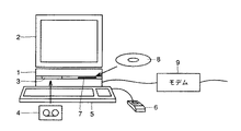
図1を参照して、本発明の実施形態1にかかる配線データ生成装置は、コンピュータ本体1、グラフィックディスプレイ装置2、磁気テープ4が装着される磁気テープ装置3、キーボード5、マウス6、CD−ROM(Compact Disc-Read Only Memory )8が装着されるCD−ROM装置7、および通信モデム9を含む。以下に述べる手法を実現するための配線データ生成プログラムは、磁気テープ4またはCD―ROM8等の記憶媒体によって供給される。この配線データ生成プログラムはコンピュータ本体1によって実行され、操作者はグラフィックディスプレイ装置2を見ながらキーボード5またはマウス6を操作することによって配線データの生成を行う。また、配線データ生成プログラムおよび他のデータは他のコンピュータより通信回線を経由し、通信モデム9を介してコンピュータ本体1に供給されてもよい。
【0034】
図2は、本発明の配線データ生成装置の構成例を示すブロック図である。図1に示すコンピュータ本体1は、CPU(Central Processing Unit )10、ROM(Read Only Memory)11、RAM(Random Access Memory)12およびハードディスク13を含む。CPU10は、グラフィックディスプレイ装置2、磁気テープ装置3、キーボード5、マウス6、CD−ROM装置7、通信モデム9、ROM11、RAM12またはハードディスク13との間でデータを入出力しながら処理を行う。磁気テープ4またはCD−ROM8に記録された配線データ生成プログラムおよび他のデータは、CPU10により磁気テープ装置3またはCD−ROM装置7を介して一旦ハードディスク13に格納される。CPU10は、ハードディスク13から適宜以下に説明するような構成を有する配線データ生成プログラムをRAM12にロードして実行することによって、クロックスキューの低減されたクロックスキューの構成方法を用いてLSI配線データの生成を行う。
【0035】
なお、以下に述べるほかの実施形態2〜実施形態6においても、装置の外観およびブロック構成は実施形態1の場合と同様である。したがって、実施形態2〜実施形態6ではハードウェア構成についての詳細な説明は繰返さない。
【0036】
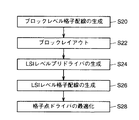
図3を参照して、実施形態1にかかるクロック構成方法は、ブロック単位で格子状のクロックラインを準備するステップ(S20)と、階層レイアウト(ブロックレイアウト)を行うステップ(S22)と、LSIレベルのレイアウトをしLSIレベルプリドライバを生成するステップ(S24)と、LSIレベルでのクロックラインを生成するステップ(S26)と、格子点ドライバの最適化を行うステップ(S28)とを含む。各ステップでの処理の内容について以下に説明する。
【0037】
まずS20では、たとえば従来のものと同様の手法によってブロック単位の格子状のクロックラインを準備する。この格子の目の大きさは任意でよい。ただし、実施形態1の装置ではこのとき、必ずブロックの最外周を取り囲むクロックラインを準備する。図4に、このステップで準備された各ブロック39a〜39dを示す。各ブロック39a〜39dはそれぞれ、クロックライン34a〜34dを含む。これら各クロックライン34a〜34dが、各ブロックの最外周を囲むクロックラインを含んでいることに注意されたい。
【0038】
次にS22で階層レイアウトを行う。クロックラインに直接関係するのはフリップフロップ(FF)であるので、クロックラインに対して具体的にはFFの配置と配線とを行い、FFのクロック入力端子をクロックライン34a〜クロックライン34dに接続する。またこのときすべてのブロックでのすべての配置配線はそれぞれのブロックの最外周のクロックラインに囲まれた範囲内で行う。
【0039】
すべての階層レイアウトが完成すれば、S24でLSIレベルでのレイアウトが行われる。ここでは、階層単位でレイアウト配置した後、従来と同様の手法でクロック入力からクロックバッファおよびプリドライバを構成する。
【0040】
最後に、S26でLSIレベルで格子配線が行われる。ここでの配線手法がこの実施形態1での特色部分である。ここでは、こうして生成するクロックラインが、あらかじめ配置された各階層の最外周のクロックラインに対してその階層の外側から交差する時、その交点でクロックラインの生成を停止する。そして、該当する階層の対辺側の同じ位置からクロックラインの生成を再開する。こうして、階層内にはLSIレベルのクロックラインを生成しないようにする。またLSIレベルのクロックラインと各階層内の最外周のクロックラインの交点においては、それぞれ対応する信号を短絡する。このようにしてLSIレベルのクロックを構成すると、図5に示す構成が得られる。
【0041】
こうして構成されたクロック回路に対して、LSIレベルまたは各階層内に存在する格子点ドライバの駆動能力を最適化する(S28)が、このときの手法は従来と同様でよい。
【0042】
この方法によれば、LSIレベルのクロックライン34と各階層のクロックライン34a〜34dとでLSI全体のクロックラインが構成されている。クロック構成の観点から見れば、これは従来のようにLSIレベルで一括して配置配線を行う場合と同様のクロック構成である。一方、この方法では従来の手法では困難であった階層レイアウトをも可能としている。すなわち、この方法によれば、従来のようにLSIレベルで一括して配置配線を行う場合と同様の優れたスキュー管理を、階層レイアウトで実現できる。
【0043】
クロックライン34a〜34dを階層単位で構成しているので、階層レイアウトが可能となる。さらにまたLSIレベルでのクロックライン34は、各階層のブロックの最外周で終端される。その結果、LSIレベルでのクロックラインが階層レイアウトに影響を与えることもない。
【0044】
階層単位で配置のシフトが発生した場合でも、LSIレベルでのクロックライン34は各階層のクロックライン34a〜34dの最外周までしかのびておらず、階層内のレイアウトとは無縁であるため、階層単位での配置に制約が課されることがなく、再度適切な位置に各ブロックの配置配線を行うことができる。
【0045】
以上のようにこの実施形態1によれば、階層レイアウトを行いながら、一括レイアウトと同様のスキュー管理を行うことができるという効果がある。
【0046】
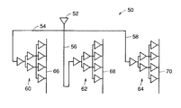
なお、S24で生成されるLSIプリドライバとしてはたとえば、図6に示すようなツリー状のプリドライバを用いることもできるし、図7に示すように等長配線54〜58によってツリー状のプリドライバ60〜64をクロックバッファ52と接続したプリドライバ50を用いてもよい。各ツリー状のプリドライバ60〜64は、たとえば各ブロック内の格子状のクロックライン66〜70に接続される。
[実施形態2]
図8を参照して、この発明の実施形態2にかかるクロック構成方法は、LSIレベル格子配線の仮生成を行うステップS80と、ブロックレベルの格子配線の切出し(詳細は後述)を行うステップS82と、後述するようにLSIレベルのクロックラインと各ブロックのクロックラインとの境界部分にタップ配線(詳細は後述)を付加するステップS84と、ブロックレイアウトを行うステップS86と、LSIレベルのプリドライバを生成するステップS88と、LSIレベルの格子配線を生成するステップS90と、最終的に格子点ドライバを最適化するステップS92とを含む。
【0047】
階層レイアウトでは、あらかじめLSIレベルでの各階層の大きさおよび配置位置などを考慮してからレイアウト作業を開始するのが通常である。この段階でまずS80の処理を行う。
【0048】
S80では、階層レイアウトを開始する前の段階での各階層の配置情報をもとにLSIレベルでの仮のクロックライン104を生成する。このLSIレベルでの仮のクロックライン104は従来と同様の手法で生成することができる。
【0049】
次にS82において、こうして構成されたLSIレベルでの仮のクロックライン104のうち、各階層内を通過する部分を切出し削除する。さらに、S84において、LSIレベルでの仮のクロックライン104の残った部分と各ブロック内部との間の境界に、LSIレベルでの仮のクロックライン104と交差する(実施形態2では直交する)方向にタップ配線113a〜113dを設ける。そしてブロック内のクロックライン104aが各タップ配線113a〜113dと接続される。図9では左上のブロック109aのみの例を示すが、他のブロック109b〜109dも同様である。
【0050】
以下は実施形態1の場合と同様である。次に、S86でブロックレイアウトが行われる。この処理では、各ブロック内で切出されたクロックラインをもとにブロック内のレイアウトを行う。次にLSIレベルでの各ブロックの最終の配置を行う。すなわち、LSIレベルプリドライバの生成が行われる(S88)。このときの各ブロックの配置は、必ずしも当初想定された配置と完全に一致する必要はない。タップ配線113a等が存在しているために、この範囲で各ブロックを左右上下に移動してもLSIレベルでの仮のクロックライン104と各ブロック内のクロックラインとの接続を確保することができる。
【0051】
さらに最終的なSLIレベル格子配線の生成が行われて(S90)、最後に全体的なクロックラインの配置配線に基づいて格子点ドライバの最適化が行われる(S92)。
【0052】
図10に、最終的に得られたLSIレイアウトを示す。この図10では、ブロック109aは当初の位置と同じ位置に、ブロック109bは左に、ブロック109cは下に、ブロック109dは右と左下に、それぞれシフトしている。
【0053】
以上のようにこの実施形態2によれば、階層レイアウト前にあらかじめ想定された各階層の大きさや配置位置を考慮して構成したLSIレベルのクロックラインを切出して使用する。そのため実施形態1で必要であったような、最外周のクロックラインなどを設ける必要はない。そのためクロックラインの総配線長を削減し消費電力を削減できるという効果がある。
【0054】
また、切出したクロックラインの境界にタップ配線を設けた。そのため、タップ配線長内で各ブロック配置の移動が可能となる。もちろん任意の位置にブロックを配置することはできないが、ブロックの位置をLSIレベルでの仮のクロックライン104の格子の目よりも小さな範囲で移動させることが可能となる。実際には、各階層の大きさや配置位置が階層レイアウトの前後で極端に変わることは少ないので、適切なタップ配線長を設定することで、実用的な範囲でのブロックの再配置が可能となる。なおタップ配線長をどのように定めるかは各LSIの設計要求によって異なるが、主として経験的に定められる。
[実施形態3]
実施形態2では、あらかじめタップ配線113aなどを設けておく。しかし、このようにタップ配線を用いなくとも階層レイアウトを可能とする方法がある。以下、そうした実施形態3について説明する。
【0055】
図11を参照して、実施形態3では、あらかじめ階層の境界において仮生成されていたLSIレベルでのクロックライン134をブロックの境界で切出して階層のレイアウトを行う。
【0056】
実施形態3のクロックラインの構成方法は、図8と比較して、S84が省略されていることと、S90とS92との間にブロック/LSI格子の接続配線を生成するステップS120を新たに含む点で異なる。以下では、実施形態2と異なる点のみ説明する。
【0057】
S80においては、あらかじめLSIレベルでのクロックライン134を生成する際に、階層の境界においてLSIレベルでのクロックライン134の生成を停止する。
【0058】
ステップS120では、図12を参照して、あらかじめ切出した階層部分のクロックライン134a〜134dと、LSIレベルでのクロックライン134とを接続する。このときに階層の境界上で最短距離にあるもの同士を接続するクロックライン接続配線144a〜144dを生成する。このようにして、各階層に対してクロックラインを構成していく。
【0059】
実施形態3によれば、たとえば仮生成の際に配置された階層の位置と、実際のLSIレベルでのレイアウトとで階層の配置位置が変わらない階層(図12のブロック139a)では、実施形態2においては必ず生成されていたタップ配線のような不要な配線が生成されない。他のブロックでも、生成されるクロックライン接続配線の配線長を最小に抑えることができる。そのため消費電力の点でより有利である。またこの実施形態3では、ブロックの配置位置が当初の想定位置よりも極端に移動してしまった場合でも対応することができる。
[実施形態4]
実施形態3では、仮配線されたLSIレベルでのクロックライン134から切出したクロックラインを階層のクロックラインとして使用した。しかし、実施形態1で示したように、各階層毎にあらかじめクロックライン34a〜34dを準備してもよい。実施形態4はそうした手法を用いる。
【0060】
図13を参照して、この実施形態4のクロック構成手法は、図3に示される手法と比較して、図3のS28に替えて、ブロック/LSI格子の接続配線生成処理のステップS150と、格子点ドライバの最適化処理のステップS92とを含む点が異なる。以下では実施形態1と異なる点についてのみ説明する。
【0061】
図14にこの実施形態4によって構成されたLSI161を示す。このLSI161では、LSIレベルでのクロックライン164の、各ブロック169a〜169dの領域以外の部分と、各ブロック169a〜169d内のクロックライン164a〜164d(横方向)、181b、181c(縦方向)とが、クロックライン接続配線174a〜クロックライン接続配線174dによって接続される。
【0062】
この実施形態4では、LSIレベルでのクロックライン164と各階層のブロック169a〜169dの縦横のクロックライン数は必ずしも一致する必要はない。例えばこれらを接続する際に、クロックラインの数の多い方を始点として、他方の最短のクロックラインへ接続するようにクロックラインの接続配線を生成することで、未接続のクロックラインがないようにする。
【0063】
図14に示されるブロック169aでは、縦方向のクロックラインに関して、LSIレベルではクロックライン181aの1本のみであるのに対して、ブロック内ではクロックライン181b、181cの2本である。そこで、階層側を始点としてクロックライン接続配線クロックライン接続配線174a〜174dを生成する。すなわち、クロックライン181bとクロックライン181aとがクロックライン接続配線174aにより接続され、クロックライン181cとクロックライン181aとがクロックライン接続配線174cによりが接続される。
【0064】
この実施形態4の方法によれば、LSIレベルと階層レベルでのクロック配線間隔が異なるものであっても扱える。そのため各階層ごとに最適なクロックライン幅を選択することができる。また同一の手法で他のLSIでレイアウト済みの階層を流用する場合、クロックライン間隔を合わせるために再度配置配線を行う必要がない。そのため実施形態4の方法によればレイアウトごと他のLSI設計を流用することが容易であるという長所がある。
[実施形態5]
以上の実施形態1から実施形態4の説明では、1つのLSIに1つの手法のみを用いる方法について説明した。しかし、互いに異なる手法を組み合わせることもできる。たとえば、上記した実施形態1から実施形態4の手法を全て組合わせてクロック構成した例を図15に示す。図15では、実施形態1〜実施形態4と同じ部品には同じ参照符号を付し、それらについての詳細な説明は繰返さない。
【0065】
図15では、実施形態1の手法をブロック39aに、実施形態2の手法をブロック109bに、実施形態3の手法をブロック139cに、実施形態4の手法をブロック169dに、それぞれ適用している。
【0066】
このように各方法を混在して使用することで、各階層毎に最適なクロックライン構成の方法を採用することができる。その結果、LSI全体として最も効率的なクロックライン構成を行うことができる。また、他のLSIの階層レイアウトを流用する場合でも、手法が特定のものと一致している必要ないので、レイアウトの再利用範囲を広げることができる。
[実施形態6]
上記した実施形態1〜実施形態5はいずれもクロックラインの構成方法に関していた。しかし、本願発明の配線生成方法はクロックラインのみに適用可能なわけではなく、階層レイアウトにおいてLSIレベルと各階層間を接続しながら回路全体にほぼ均等に配線を巡らす必要がある場合には同様に適用できる。
【0067】
その一例は、LSIレベルで性能管理を要求される配線として知られている電源/グランド配線がある。グランドラインも、一定の電位を回路に与えるという意味では電源ラインと同様であると考えられる。したがって電源ラインといえばグランドラインをも含むと考えてよい。電源/グランド配線は、LSIレベルで外部からの電源/グランドの供給箇所を複数個持ち、LSI内の全トランジスタに対して動作を保証できるだけの供給能力を持つ必要がある。このため、クロックと同様にLSIレベルでの均一な供給能力が要求される。
【0068】
上記した方法はいずれも、そのまま電源/グランド配線に適用することができる。図16に、実施形態1〜実施形態4に記載した方法を全て適用して電源/グランド配線を行ったLSI201を示す。この例でも、実施形態5と同様、実施形態1〜実施形態4と同じ部品には同じ参照符号を付した。このようにして電源/グランド配線を構成することで、階層レイアウトを行いつつ安定した供給能力を実現することができる。
【0069】
今回開示された実施の形態はすべての点で例示であって制限的なものではないと考えられるべきである。本発明の範囲は上記した説明ではなくて特許請求の範囲によって示され、特許請求の範囲と均等の意味および範囲内でのすべての変更が含まれることが意図される。
【0070】
【発明の効果】
以上のように請求項1に記載の発明によれば、LSIレベルの格子配線を、ブロックを単位とした階層レイアウトを用いて、ブロック内の配線と別に行うことができる。そのため、階層レイアウトを用いながら、クロックスキューを低減させたり電源を安定に供給したりするための配線を行うことが可能となる。
また、ブロック内の格子配線の各々を、LSIレベルの格子配線と接続することができる。LSIレベルの格子配線がブロック内のレイアウトに影響を与えることがない。そのため階層レイアウトを十分に利用することができる。
【0073】
請求項2に記載の発明によれば、ブロックの境界部分においてLSIレベルの格子配線にタップ線を設けることにより、ブロックを移動させても、それがタップ線の長さの範囲内である限りブロック内の格子配線とLSIレベルの格子配線との接続を保つことができる。したがってブロックのレイアウトが柔軟に行え、階層レイアウトを十分に利用することができる。
【0074】
請求項3に記載の発明によれば、ブロックの移動量が大きくなっても格子配線同士の接続は容易であるため階層レイアウトが柔軟に行える。そのため、階層レイアウトの利点を十分に活用することができる。
【0075】
請求項4に記載の発明によれば、既にある他の大規模集積回路の設計においてどの手法が用いられていたかに関係なく、容易にそうした設計データを階層レイアウトに流用することができる。その結果、過去の資産を生かしながら、階層レイアウトを用いて設計要求に応じた配置配線を行うことができる。
【0076】
請求項5に記載の発明によれば、既にある他の大規模集積回路の設計においてどの手法が用いられていたかに関係なく、容易にクロックラインに関する設計データを階層レイアウトに流用することができる。その結果、過去の資産を生かしながら、階層レイアウトを用いてクロックスキューに関する設計要求に応じた配置配線を行うことができる。
【0077】
請求項6に記載の発明によれば、既にある他の大規模集積回路の設計においてどの手法が用いられていたかに関係なく、容易に電源ラインに関する設計データを階層レイアウトに流用することができる。その結果、過去の資産を生かしながら、階層レイアウトを用いて電源ラインに関する設計要求に応じた配置配線を行うことができる。
【図面の簡単な説明】
【図1】 本願発明の実施の形態の装置の外観図である。
【図2】 本願発明の実施の形態の装置のハードウェアブロック図である。
【図3】 本願発明の実施形態1の装置の処理の流れを示すフローチャートである。
【図4】 実施形態1の処理対象となるブロックの例を示す平面図である。
【図5】 実施形態1の装置によるLSIレイアウト例を示す平面図である。
【図6】 ツリープリドライバの例を示す模式図である。
【図7】 等長配線によるプリドライバの配置を示す模式図である。
【図8】 実施形態2の装置の処理の流れを示すフローチャートである。
【図9】 実施形態2の装置によるLSIレイアウトの例を示す平面図である。
【図10】 実施形態2の装置によるLSIの最終レイアウトの例を示す平面図である。
【図11】 実施形態3の装置の処理の流れを示すフローチャートである。
【図12】 実施形態3の装置によるLSIレイアウトの例を示す平面図である。
【図13】 実施形態4の装置の処理の流れを示すフローチャートである。
【図14】 実施形態4の装置によるLSIレイアウトの例を示す平面図である。
【図15】 実施形態5の装置によるLSIレイアウトの例を示す平面図である。
【図16】 実施形態6の装置によるLSIレイアウトの例を示す平面図である。
【図17】 従来の技術におけるクロック構成手法を示す、LSIの平面図である。
【図18】 従来の技術におけるクロックスキューの低減の一手法を示す、LSIの平面図である。
【符号の説明】
31,101,131,161,181,201,221 LSI、32 クロックバッファ、33a,b プリバッファ、34a〜d,104a〜d,134a〜d,174a〜d クロックライン、39a〜d,109a〜d,139a〜d,169a〜d ブロック。[0001]
BACKGROUND OF THE INVENTION
The present invention relates to a wiring data generation method such as a clock line configuration corresponding to a hierarchical layout, and in particular, wiring data generation capable of flexible block layout adjustment at an LSI (Large Scale Integrated Circuit) level according to a design request. The present invention relates to methods and large scale integrated circuit devices designed by such methods.
[0002]
[Prior art]
It is difficult to accurately supply clocks to all the sequential elements existing in the LSI at the same time, and there is a time difference between the clocks supplied to the respective units. This time difference is called clock skew. In particular, as the LSI density increases and the circuit scale increases, the clock skew given to each part of the LSI needs to be an extremely small value, and how to reduce the clock skew becomes a problem. Since such clock skew occurs mainly at the design stage, highly accurate skew management is required when configuring the clock.
[0003]
Referring to FIG. 17, the conventional skew management method uses an LSI.221 input CLK to LSI22The clock signal supplied to 1 is an LSI221 is supplied to the pre-buffer 103 through the
[0004]
In an actual LSI, the
[0005]
Therefore LSI22The skew is reduced by adjusting the driving capability of the
[0006]
In this method, the output of the
[0007]
On the other hand, when the LSI becomes larger, a so-called hierarchical layout becomes necessary. Hierarchical layout is a technique introduced to efficiently perform LSI layout. In the hierarchical layout method, the LSI is divided into several blocks, the layout is first performed in units of blocks, and the blocks for which the layout has been completed are optimally placed and routed again to lay out the entire LSI. In some cases, a layer that has already been laid out in another LSI is reused. In this case as well, a hierarchical layout is required.
[0008]
Referring to FIG. 18, the clock configuration method in the conventional hierarchical layout is as follows. First, the layout of the
[0009]
When all the layouts of each hierarchy are completed, the
[0010]
[Problems to be solved by the invention]
When hierarchical layout is performed in this way, there are the following three types of skew.
[0011]
(1) Skew of clock configured in each block
(2) Skew due to clock distribution from clock CLK to each block
(3) Skew based on delay elements for clock delay compensation
As described above, since there are three types of occurrence of skew, it is essentially very difficult to reduce the skew.
[0012]
On the other hand, in the method of configuring the clock in the entire LSI, the cause of skew is only the skew of the configured clock, resulting in low skew. If a hierarchical layout is attempted using this method, there are grid-like clock wirings that are stretched across the entire LSI in advance, so when placing a block, the clock wiring in the block and the LSI clock wiring overlap. There is a restriction that only blocks can be placed. Therefore, layout with this method is difficult.
[0013]
For example, if one block completes the layout first and then the next block that completed the layout becomes larger than the expected size, the layout position of the enlarged block is secured. In order to do this, it may be necessary to move the block whose layout has been completed first from the originally planned arrangement position. In such a case, since the lattice-like clock wiring stretched over the entire LSI cannot move, the block can only move in units of lattices. As a result, there is a problem that optimal arrangement adjustment of each block at the LSI level becomes impossible and the advantages of the hierarchical layout are lost.
[0014]
Therefore, an object of the present invention is to provide a method for configuring a low skew clock corresponding to a hierarchical layout.
[0015]
Another object of the present invention is to provide a method for constructing a low skew clock capable of arranging and adjusting each block more flexibly in accordance with a hierarchical layout.
[0016]
Still another object of the present invention is to provide a large-scale integrated circuit device capable of realizing a placement and routing which is scared of design requirements while making full use of past assets.
[0017]
[Means for Solving the Problems]
A wiring data generation method according to a first aspect of the present invention is a wiring data generation method for generating wiring data when designing an LSI with a hierarchical layout, the step of generating block level grid wiring, And a step of generating LSI-level grid wiring outside the block area of the LSI.Therefore, the step of generating the block level lattice wiring includes the step of generating the lattice wiring inside the block at an appropriate interval with respect to the block, and the step of generating the LSI level lattice wiring includes the step of generating the block level lattice wiring. Generating a connection wiring for connecting each to the LSI level grid wiring closest to the block level grid wiring.
[0018]
Since LSI-level grid wiring is generated separately from the grid wiring in a block, LSI wiring data can be generated using a hierarchical layout in units of blocks.
[0022]
Also,Each of the grid lines in the block can be connected to an LSI level grid line. LSI-level grid wiring does not affect the layout in the block.
[0023]
Claim2The wiring data generation method according to the invention described in
[0024]
By providing tap lines to LSI-level grid wiring at the boundary of the block, even if the block is moved, as long as it is within the length of the tap line, the lattice wiring in the block and the LSI-level grid wiring Can stay connected. Therefore, the layout of the block can be performed flexibly.
[0025]
Claim3The wiring data generation method according to the invention described in
[0026]
The block can be moved by cutting the LSI level lattice wiring at the boundary of the block. After the movement, if the grid wiring in the block is connected to the LSI level grid wiring, a necessary signal can be supplied to each block. Even if the amount of movement of the block increases, the hierarchical wiring can be flexibly performed because the grid wirings can be easily connected.
[0027]
Claim4A large-scale integrated circuit device according to the invention described in claim1~ Claim3Including a block arranged by using any two or more of the wiring data generation methods and lattice wiring at the LSI level.
[0028]
Claim1~ Claim3Any of the wiring data generation methods described in (1) can be freely selected. Therefore, such design data can be easily applied to the hierarchical layout regardless of which method is used in the design of another existing large-scale integrated circuit.
[0029]
Claim5A large-scale integrated circuit device according to the invention described in claim4In addition to the configuration of the invention described in (1), the lattice wiring includes a clock line.
[0030]
Claim1~ Claim3Any of the wiring data generation methods described in (1) can be freely selected. Therefore, the design data relating to the clock line can be easily used for the hierarchical layout regardless of which method is used in the design of another already existing large-scale integrated circuit.
[0031]
Claim6A large-scale integrated circuit device according to the invention described in claim4In addition to the configuration of the invention described in (1), the grid wiring includes a power supply line.
[0032]
Claim1~ Claim3Any of the wiring data generation methods described in (1) can be freely selected. Therefore, the design data relating to the power supply line can be easily used for the hierarchical layout regardless of which method is used in the design of another already existing large-scale integrated circuit.
[0033]
DETAILED DESCRIPTION OF THE INVENTION
[Embodiment 1]
Referring to FIG. 1, a wiring data generation apparatus according to
[0034]
FIG. 2 is a block diagram showing a configuration example of the wiring data generation apparatus of the present invention. A computer
[0035]
In
[0036]
Referring to FIG. 3, the clock configuration method according to the first embodiment includes a step of preparing a grid-like clock line in block units (S20), a step of performing hierarchical layout (block layout) (S22), an LSI level, and the like. And a step of generating an LSI level pre-driver (S24), a step of generating a clock line at the LSI level (S26), and a step of optimizing the lattice point driver (S28). The contents of processing in each step will be described below.
[0037]
First, in S20, a block-like lattice-like clock line is prepared, for example, by a method similar to the conventional one. The size of the grid may be arbitrary. However, in the apparatus of the first embodiment, a clock line that always surrounds the outermost periphery of the block is prepared. FIG. 4 shows the
[0038]
Next, a hierarchical layout is performed in S22. Since the flip-flop (FF) is directly related to the clock line, the FF is specifically arranged and wired with respect to the clock line, and the clock input terminal of the FF is connected to the
[0039]
When all hierarchical layouts are completed, layout at the LSI level is performed in S24. Here, after the layout is arranged in hierarchical units, the clock buffer and the pre-driver are configured from the clock input by the same method as in the prior art.
[0040]
Finally, in S26, lattice wiring is performed at the LSI level. The wiring method here is the special color portion in the first embodiment. Here, when the clock line thus generated intersects from the outside of the outermost clock line of each hierarchy arranged in advance, the generation of the clock line is stopped at the intersection. Then, the generation of the clock line is resumed from the same position on the opposite side of the corresponding hierarchy. Thus, LSI level clock lines are not generated in the hierarchy. At the intersection of the LSI level clock line and the outermost clock line in each layer, the corresponding signals are short-circuited. When the LSI level clock is configured in this way, the configuration shown in FIG. 5 is obtained.
[0041]
For the clock circuit thus configured, the driving capability of the lattice point driver existing in the LSI level or in each layer is optimized (S28), but the method at this time may be the same as the conventional one.
[0042]
According to this method, the LSI-
[0043]
Since the
[0044]
Even when an arrangement shift occurs in units of layers, the
[0045]
As described above, according to the first embodiment, it is possible to perform the skew management similar to the collective layout while performing the hierarchical layout.
[0046]
As the LSI pre-driver generated in S24, for example, a tree-shaped pre-driver as shown in FIG. 6 can be used, or as shown in FIG. A pre-driver 50 in which 60 to 64 are connected to the clock buffer 52 may be used. Each tree-
[Embodiment 2]
Referring to FIG. 8, the clock configuration method according to the second embodiment of the present invention includes step S80 for temporarily generating LSI level lattice wiring, and step S82 for cutting out block level lattice wiring (details will be described later). As described later, step S84 for adding tap wiring (details will be described later) to the boundary between the LSI level clock line and the clock line of each block, step S86 for block layout, and generation of the LSI level pre-driver Step S88, step S90 for generating LSI-level lattice wiring, and step S92 for finally optimizing the lattice point driver.
[0047]
In the hierarchical layout, the layout work is usually started after taking into account the size and arrangement position of each hierarchy at the LSI level in advance. At this stage, first, the process of S80 is performed.
[0048]
In S80, a
[0049]
Next, in S82, a portion passing through each layer is cut out and deleted from the
[0050]
The following is the same as in the first embodiment. Next, block layout is performed in S86. In this process, the layout in the block is performed based on the clock line cut out in each block. Next, the final arrangement of each block at the LSI level is performed. That is, an LSI level pre-driver is generated (S88). The arrangement of each block at this time does not necessarily need to completely match the initially assumed arrangement. Since the
[0051]
Further, the final SLI level grid wiring is generated (S90), and finally the grid point driver is optimized based on the overall clock line arrangement and wiring (S92).
[0052]
FIG. 10 shows the finally obtained LSI layout. In FIG. 10, the
[0053]
As described above, according to the second embodiment, an LSI level clock line configured in consideration of the size and arrangement position of each layer assumed before the layer layout is cut out and used. Therefore, there is no need to provide the outermost clock line or the like as required in the first embodiment. Therefore, there is an effect that the total wiring length of the clock line can be reduced and power consumption can be reduced.
[0054]
In addition, tap wiring is provided at the boundary of the cut clock line. Therefore, each block arrangement can be moved within the tap wiring length. Of course, the block cannot be arranged at an arbitrary position, but the position of the block can be moved within a range smaller than the lattice of the
[Embodiment 3]
In the second embodiment,
[0055]
Referring to FIG. 11, in the third embodiment, the layout of the hierarchy is performed by cutting out the
[0056]
Compared with FIG. 8, the clock line configuration method of the third embodiment newly includes step S120 in which S84 is omitted and a connection wiring of a block / LSI lattice is generated between S90 and S92. It is different in point. Hereinafter, only points different from the second embodiment will be described.
[0057]
In S80, when the
[0058]
In step S120, referring to FIG. 12, the
[0059]
According to the third embodiment, for example, in a hierarchy (
[Embodiment 4]
In the third embodiment, the clock line cut out from the temporarily wired LSI
[0060]
Referring to FIG. 13, the clock configuration method of the fourth embodiment is different from the method shown in FIG. 3 in place of S28 of FIG. The difference is that it includes step S92 of the optimization process of the lattice point driver. Only differences from the first embodiment will be described below.
[0061]
FIG. 14 shows an
[0062]
In the fourth embodiment, the number of clock lines in the vertical and horizontal directions of the
[0063]
In the
[0064]
According to the method of the fourth embodiment, even if the clock wiring intervals at the LSI level and the hierarchical level are different, they can be handled. Therefore, an optimal clock line width can be selected for each layer. In addition, when a layer that has been laid out by another LSI is diverted using the same method, there is no need to perform placement and routing again in order to adjust the clock line interval. Therefore, according to the method of the fourth embodiment, there is an advantage that it is easy to divert other LSI designs for each layout.
[Embodiment 5]
In the above description of the first to fourth embodiments, the method using only one method for one LSI has been described. However, it is possible to combine different methods. For example, FIG. 15 shows an example in which a clock is configured by combining all the methods of the first to fourth embodiments described above. In FIG. 15, the same components as those in the first to fourth embodiments are denoted by the same reference numerals, and detailed description thereof will not be repeated.
[0065]
In FIG. 15, the method of the first embodiment is applied to the
[0066]
By using the methods in a mixed manner in this way, it is possible to adopt a method of optimal clock line configuration for each layer. As a result, the most efficient clock line configuration can be performed for the entire LSI. In addition, even when a hierarchical layout of another LSI is used, the layout reuse range can be expanded because the method does not need to match a specific one.
[Embodiment 6]
The first to fifth embodiments described above all relate to the clock line configuration method. However, the wiring generation method of the present invention is not applicable only to the clock line, and in the case where it is necessary to circulate the wiring almost uniformly over the entire circuit while connecting the LSI level and each layer in the hierarchical layout. Applicable.
[0067]
One example is a power / ground wiring known as a wiring that requires performance management at the LSI level. The ground line is also considered to be similar to the power supply line in the sense that a constant potential is applied to the circuit. Therefore, it can be considered that the power supply line includes the ground line. The power supply / ground wiring has a plurality of external power supply / ground supply locations at the LSI level, and needs to have a supply capability sufficient to guarantee the operation of all the transistors in the LSI. For this reason, a uniform supply capability at the LSI level is required as with the clock.
[0068]
Any of the above methods can be applied to the power / ground wiring as it is. FIG. 16 shows an
[0069]
The embodiment disclosed this time should be considered as illustrative in all points and not restrictive. The scope of the present invention is defined by the terms of the claims, rather than the description above, and is intended to include any modifications within the scope and meaning equivalent to the terms of the claims.
[0070]
【The invention's effect】
As described above, according to the first aspect of the present invention, LSI level lattice wiring can be performed separately from wiring in a block by using a hierarchical layout in units of blocks. For this reason, it is possible to perform wiring for reducing clock skew and supplying power stably while using a hierarchical layout.
In addition, each of the grid lines in the block can be connected to the LSI level grid line. LSI-level grid wiring does not affect the layout in the block. Therefore, the hierarchical layout can be fully utilized.
[0073]
Claim2According to the invention described in the above, even if the block is moved by providing the tap line to the LSI level lattice wiring at the boundary portion of the block, as long as it is within the length of the tap line, The connection between the wiring and the lattice wiring at the LSI level can be maintained. Therefore, the block layout can be flexibly performed and the hierarchical layout can be fully utilized.
[0074]
Claim3According to the invention described in (1), the hierarchical layout can be flexibly performed because the grid lines can be easily connected to each other even if the amount of movement of the block increases. Therefore, the advantages of the hierarchical layout can be fully utilized.
[0075]
Claim4According to the invention described in (1), such design data can be easily diverted to the hierarchical layout regardless of which method is used in the design of another existing large-scale integrated circuit. As a result, it is possible to perform placement and routing according to the design request using the hierarchical layout while utilizing the past assets.
[0076]
Claim5According to the invention described in (1), design data relating to the clock line can be easily used in the hierarchical layout regardless of which method is used in the design of another existing large-scale integrated circuit. As a result, it is possible to perform placement and routing in accordance with design requirements related to clock skew using a hierarchical layout while making use of past assets.
[0077]
Claim6According to the invention described in (1), the design data relating to the power supply line can be easily diverted to the hierarchical layout regardless of which method has been used in the design of another existing large-scale integrated circuit. As a result, it is possible to perform placement and routing in accordance with the design requirements related to the power supply line using the hierarchical layout while utilizing the past assets.
[Brief description of the drawings]
FIG. 1 is an external view of an apparatus according to an embodiment of the present invention.
FIG. 2 is a hardware block diagram of an apparatus according to an embodiment of the present invention.
FIG. 3 is a flowchart showing a process flow of the apparatus according to the first embodiment of the present invention.
FIG. 4 is a plan view showing an example of a block to be processed in the first embodiment.
5 is a plan view showing an LSI layout example by the apparatus of
FIG. 6 is a schematic diagram illustrating an example of a tree pre-driver.
FIG. 7 is a schematic diagram showing the arrangement of pre-drivers with equal-length wiring.
FIG. 8 is a flowchart illustrating a processing flow of the apparatus according to the second embodiment.
FIG. 9 is a plan view showing an example of an LSI layout by the apparatus of the second embodiment.
FIG. 10 is a plan view showing an example of the final layout of an LSI by the apparatus of the second embodiment.
FIG. 11 is a flowchart illustrating a processing flow of the apparatus according to the third embodiment.
12 is a plan view showing an example of an LSI layout by the apparatus of
FIG. 13 is a flowchart illustrating a processing flow of the apparatus according to the fourth embodiment.
FIG. 14 is a plan view showing an example of an LSI layout by the apparatus of the fourth embodiment.
15 is a plan view showing an example of an LSI layout by the apparatus of
FIG. 16 is a plan view showing an example of an LSI layout by the apparatus of the sixth embodiment.
FIG. 17 is a plan view of an LSI showing a clock configuration method in the prior art.
FIG. 18 is a plan view of an LSI showing one method for reducing clock skew in the prior art.
[Explanation of symbols]
31, 101, 131, 161, 181, 201, 221 LSI, 32 clock buffer, 33a, b pre-buffer, 34a-d, 104a-d, 134a-d, 174a-d clock line, 39a-d, 109a-d , 139a-d, 169a-d blocks.
Claims (6)
ブロックレベル格子配線を生成するステップと、
ブロック内のレイアウトを実行するステップと、
LSIの、前記ブロックの領域以外においてLSIレベルの格子配線を生成するステップとを含み、
前記ブロックレベル格子配線を生成する前記ステップは、ブロック内部の格子配線を当該ブロックに対して適切な間隔で生成するステップを含み、
前記LSIレベルの格子配線を生成する前記ステップは、前記ブロックレベルの格子配線の各々を、前記ブロックレベルの格子配線にそれぞれ最も近い前記LSIレベルの格子配線に接続する接続配線を生成するステップを含む、配線データ生成方法。A wiring data generation method for generating wiring data when designing an LSI with a hierarchical layout,
Generating block level grid wiring; and
Performing the layout in the block;
The LSI, and generating a grid interconnection of LSI levels in other regions of said block look including,
The step of generating the block level grid wiring includes generating grid wiring inside the block at appropriate intervals with respect to the block,
The step of generating the LSI level grid wiring includes generating a connection wiring for connecting each block level grid wiring to the LSI level grid wiring closest to the block level grid wiring. Wiring data generation method.
LSIレベルの格子配線を仮生成するステップと、
仮生成された前記LSIレベルの格子配線の各々について、配置されるブロックの領域内の部分との境界を規定するステップと、
前記境界の各々に、前記格子配線と交差する方向のタップ線を生成するステップと、
各前記ブロック内の格子配線が前記対応するタップ線と接続可能な範囲で各ブロックの移動を許容してブロックレイアウトを行うステップと、
LSIレベルの格子配線を生成するステップとを含む、配線データ生成方法。A wiring data generation method for generating wiring data when designing an LSI with a hierarchical layout,
Provisionally generating LSI level lattice wiring;
For each of the temporarily generated LSI level lattice wirings, defining a boundary with a portion in a region of a block to be arranged;
Generating a tap line in a direction intersecting the grid wiring at each of the boundaries;
Performing a block layout by allowing movement of each block within a range in which the grid wiring in each block can be connected to the corresponding tap line;
A wiring data generation method including a step of generating an LSI level lattice wiring.
LSIレベルの格子配線を仮生成するステップと、
仮生成された前記LSIレベルの格子配線の各々について、配置されるブロックの領域内の部分との境界を規定するステップと、
各ブロックの移動を許容して、各前記境界で前記格子配線を切断してブロックレイアウトを行うステップと、
前記ブロックレイアウトを行うステップによって移動したブロック内の格子配線と、ブロック外の格子配線とを接続する配線を生成するステップと、
LSIレベルの格子配線を生成するステップとを含む、配線データ生成方法。A wiring data generation method for generating wiring data when designing an LSI with a hierarchical layout,
Provisionally generating LSI level lattice wiring;
For each of the temporarily generated LSI level lattice wirings, defining a boundary with a portion in a region of a block to be arranged;
Allowing each block to move, cutting the grid wiring at each of the boundaries, and performing a block layout; and
Generating a wiring that connects the grid wiring in the block moved by the step of performing the block layout and the grid wiring outside the block;
A wiring data generation method including a step of generating an LSI level lattice wiring.
Priority Applications (2)
| Application Number | Priority Date | Filing Date | Title |
|---|---|---|---|
| JP22110399A JP4315532B2 (en) | 1999-08-04 | 1999-08-04 | Wiring data generation method and large-scale integrated circuit device designed by the method |
| US09/497,172 US6546537B1 (en) | 1999-08-04 | 2000-02-03 | Wiring data generation method and wiring data generation apparatus allowing inconsistency between block internal line and block external lines |
Applications Claiming Priority (1)
| Application Number | Priority Date | Filing Date | Title |
|---|---|---|---|
| JP22110399A JP4315532B2 (en) | 1999-08-04 | 1999-08-04 | Wiring data generation method and large-scale integrated circuit device designed by the method |
Publications (3)
| Publication Number | Publication Date |
|---|---|
| JP2001044289A JP2001044289A (en) | 2001-02-16 |
| JP2001044289A5 JP2001044289A5 (en) | 2005-10-27 |
| JP4315532B2 true JP4315532B2 (en) | 2009-08-19 |
Family
ID=16761545
Family Applications (1)
| Application Number | Title | Priority Date | Filing Date |
|---|---|---|---|
| JP22110399A Expired - Fee Related JP4315532B2 (en) | 1999-08-04 | 1999-08-04 | Wiring data generation method and large-scale integrated circuit device designed by the method |
Country Status (2)
| Country | Link |
|---|---|
| US (1) | US6546537B1 (en) |
| JP (1) | JP4315532B2 (en) |
Families Citing this family (8)
| Publication number | Priority date | Publication date | Assignee | Title |
|---|---|---|---|---|
| JP2003092352A (en) * | 2001-09-18 | 2003-03-28 | Nec Corp | Clock signal distributing circuit for semiconductor integrated circuit device |
| JP2006065669A (en) * | 2004-08-27 | 2006-03-09 | Renesas Technology Corp | Automatic arrangement and wiring apparatus and program |
| WO2006054786A1 (en) * | 2004-11-19 | 2006-05-26 | Nec Corporation | Semiconductor integrated circuit wiring design system, semiconductor integrated circuit, and wiring design program |
| US7467367B1 (en) * | 2005-10-27 | 2008-12-16 | Cadence Design Systems, Inc. | Method and system for clock tree synthesis of an integrated circuit |
| JP4890180B2 (en) * | 2006-09-27 | 2012-03-07 | ルネサスエレクトロニクス株式会社 | Clock distribution circuit and test method |
| JP5112229B2 (en) * | 2008-09-05 | 2013-01-09 | 株式会社エヌ・ティ・ティ・ドコモ | Distribution device, terminal device, system and method |
| JP5080406B2 (en) * | 2008-09-05 | 2012-11-21 | 株式会社エヌ・ティ・ティ・ドコモ | Distribution device, terminal device, system and method |
| JP5842946B2 (en) * | 2014-03-24 | 2016-01-13 | ソニー株式会社 | Semiconductor integrated circuit |
Family Cites Families (4)
| Publication number | Priority date | Publication date | Assignee | Title |
|---|---|---|---|---|
| JPH08330523A (en) | 1995-06-02 | 1996-12-13 | Hitachi Ltd | Wire layout method |
| JP2874628B2 (en) * | 1996-01-30 | 1999-03-24 | 日本電気株式会社 | Apparatus and method for optimizing logic circuit |
| US6289495B1 (en) * | 1998-04-17 | 2001-09-11 | Lsi Logic Corporation | Method and apparatus for local optimization of the global routing |
| JP2001007293A (en) * | 1999-06-25 | 2001-01-12 | Mitsubishi Electric Corp | Semiconductor integrated circuit device |
-
1999
- 1999-08-04 JP JP22110399A patent/JP4315532B2/en not_active Expired - Fee Related
-
2000
- 2000-02-03 US US09/497,172 patent/US6546537B1/en not_active Expired - Fee Related
Also Published As
| Publication number | Publication date |
|---|---|
| JP2001044289A (en) | 2001-02-16 |
| US6546537B1 (en) | 2003-04-08 |
Similar Documents
| Publication | Publication Date | Title |
|---|---|---|
| US8276105B2 (en) | Automatic positioning of gate array circuits in an integrated circuit design | |
| JP5224642B2 (en) | Integrated circuit layout method and computer program | |
| US8451026B2 (en) | Integrated circuit, method of generating a layout of an integrated circuit using standard cells, and a standard cell library providing such standard cells | |
| JPH10189746A (en) | Wiring layout method for lsi logic circuit | |
| US20050274983A1 (en) | Semiconductor device and layout design method therefor | |
| US20100096757A1 (en) | Method and System for Distributing Clock Signals on Non Manhattan Semiconductor Integrated Circuits | |
| US7795943B2 (en) | Integrated circuit device and layout design method therefor | |
| JP4272647B2 (en) | Layout method of semiconductor integrated circuit device and layout program thereof | |
| US10068048B1 (en) | Generating clock trees for a circuit design | |
| US10977407B2 (en) | Superpower gating cell and integrated circuit including the same | |
| JP4315532B2 (en) | Wiring data generation method and large-scale integrated circuit device designed by the method | |
| JP2008218730A (en) | Semiconductor device designing method and program | |
| JP3629250B2 (en) | Semiconductor integrated circuit layout method and semiconductor integrated circuit | |
| JP2004252717A (en) | Method and device for designing semiconductor integrated circuit, data structure of cell library, and automatic layout program | |
| US7002253B2 (en) | Semiconductor device and design method thereof | |
| US6487707B1 (en) | Layout design system of semiconductor ic device, layout design method of semiconductor ic device and computer-readable recording medium on which programs for allowing computer to execute respective means in the system or respective steps in the method are recorded | |
| US20210004520A1 (en) | Planning method for power metal lines | |
| US8341563B1 (en) | Method and apparatus for power gating stitching | |
| US7418675B2 (en) | System and method for reducing the power consumption of clock systems | |
| JP2001044289A5 (en) | ||
| JP4261172B2 (en) | Semiconductor integrated circuit layout program and semiconductor integrated circuit layout system | |
| JP2001308189A (en) | Semiconductor integrated circuit device and method for routing clock line and recording medium | |
| KR20010070243A (en) | Method for forming wiring pattern of a semiconductor integrated circuit | |
| US6588003B1 (en) | Method of control cell placement for datapath macros in integrated circuit designs | |
| JP2009188093A (en) | Method and device for designing semiconductor integrated circuit, and program |
Legal Events
| Date | Code | Title | Description |
|---|---|---|---|
| A521 | Written amendment |
Free format text: JAPANESE INTERMEDIATE CODE: A523 Effective date: 20050729 |
|
| A621 | Written request for application examination |
Free format text: JAPANESE INTERMEDIATE CODE: A621 Effective date: 20050729 |
|
| A131 | Notification of reasons for refusal |
Free format text: JAPANESE INTERMEDIATE CODE: A131 Effective date: 20081014 |
|
| A977 | Report on retrieval |
Free format text: JAPANESE INTERMEDIATE CODE: A971007 Effective date: 20081016 |
|
| A521 | Written amendment |
Free format text: JAPANESE INTERMEDIATE CODE: A523 Effective date: 20081110 |
|
| TRDD | Decision of grant or rejection written | ||
| A01 | Written decision to grant a patent or to grant a registration (utility model) |
Free format text: JAPANESE INTERMEDIATE CODE: A01 Effective date: 20090512 |
|
| A01 | Written decision to grant a patent or to grant a registration (utility model) |
Free format text: JAPANESE INTERMEDIATE CODE: A01 |
|
| A61 | First payment of annual fees (during grant procedure) |
Free format text: JAPANESE INTERMEDIATE CODE: A61 Effective date: 20090519 |
|
| R150 | Certificate of patent or registration of utility model |
Free format text: JAPANESE INTERMEDIATE CODE: R150 |
|
| FPAY | Renewal fee payment (event date is renewal date of database) |
Free format text: PAYMENT UNTIL: 20120529 Year of fee payment: 3 |
|
| FPAY | Renewal fee payment (event date is renewal date of database) |
Free format text: PAYMENT UNTIL: 20120529 Year of fee payment: 3 |
|
| S111 | Request for change of ownership or part of ownership |
Free format text: JAPANESE INTERMEDIATE CODE: R313111 |
|
| FPAY | Renewal fee payment (event date is renewal date of database) |
Free format text: PAYMENT UNTIL: 20120529 Year of fee payment: 3 |
|
| R350 | Written notification of registration of transfer |
Free format text: JAPANESE INTERMEDIATE CODE: R350 |
|
| FPAY | Renewal fee payment (event date is renewal date of database) |
Free format text: PAYMENT UNTIL: 20120529 Year of fee payment: 3 |
|
| FPAY | Renewal fee payment (event date is renewal date of database) |
Free format text: PAYMENT UNTIL: 20130529 Year of fee payment: 4 |
|
| LAPS | Cancellation because of no payment of annual fees |