JP4312414B2 - Double use of FFT circuit by imager and transceiver - Google Patents
Double use of FFT circuit by imager and transceiver Download PDFInfo
- Publication number
- JP4312414B2 JP4312414B2 JP2002116423A JP2002116423A JP4312414B2 JP 4312414 B2 JP4312414 B2 JP 4312414B2 JP 2002116423 A JP2002116423 A JP 2002116423A JP 2002116423 A JP2002116423 A JP 2002116423A JP 4312414 B2 JP4312414 B2 JP 4312414B2
- Authority
- JP
- Japan
- Prior art keywords
- reader
- transceiver
- automatic
- data
- support
- Prior art date
- Legal status (The legal status is an assumption and is not a legal conclusion. Google has not performed a legal analysis and makes no representation as to the accuracy of the status listed.)
- Expired - Lifetime
Links
- 238000004891 communication Methods 0.000 claims description 24
- 238000000034 method Methods 0.000 claims description 7
- 238000012545 processing Methods 0.000 claims description 7
- 230000005540 biological transmission Effects 0.000 claims description 4
- 238000013480 data collection Methods 0.000 claims description 3
- 230000008569 process Effects 0.000 claims description 3
- 238000012546 transfer Methods 0.000 claims description 2
- 238000010586 diagram Methods 0.000 description 10
- 239000002131 composite material Substances 0.000 description 9
- 239000000969 carrier Substances 0.000 description 7
- 230000009977 dual effect Effects 0.000 description 5
- 238000013507 mapping Methods 0.000 description 5
- 230000003287 optical effect Effects 0.000 description 4
- 239000004065 semiconductor Substances 0.000 description 4
- 108700026140 MAC combination Proteins 0.000 description 3
- 238000004590 computer program Methods 0.000 description 3
- 238000013479 data entry Methods 0.000 description 3
- 238000013500 data storage Methods 0.000 description 3
- 238000005516 engineering process Methods 0.000 description 3
- 230000008901 benefit Effects 0.000 description 2
- 238000006243 chemical reaction Methods 0.000 description 2
- 238000003780 insertion Methods 0.000 description 2
- 230000037431 insertion Effects 0.000 description 2
- 230000007246 mechanism Effects 0.000 description 2
- 238000010587 phase diagram Methods 0.000 description 2
- 230000004044 response Effects 0.000 description 2
- 238000001228 spectrum Methods 0.000 description 2
- 208000015976 Corneal dystrophy-perceptive deafness syndrome Diseases 0.000 description 1
- 230000004913 activation Effects 0.000 description 1
- 230000006978 adaptation Effects 0.000 description 1
- 230000000712 assembly Effects 0.000 description 1
- 238000000429 assembly Methods 0.000 description 1
- 230000001413 cellular effect Effects 0.000 description 1
- 238000002592 echocardiography Methods 0.000 description 1
- 230000006870 function Effects 0.000 description 1
- 238000012986 modification Methods 0.000 description 1
- 230000004048 modification Effects 0.000 description 1
- 238000001579 optical reflectometry Methods 0.000 description 1
- 238000005070 sampling Methods 0.000 description 1
Images


Classifications
-
- H—ELECTRICITY
- H04—ELECTRIC COMMUNICATION TECHNIQUE
- H04B—TRANSMISSION
- H04B1/00—Details of transmission systems, not covered by a single one of groups H04B3/00 - H04B13/00; Details of transmission systems not characterised by the medium used for transmission
- H04B1/38—Transceivers, i.e. devices in which transmitter and receiver form a structural unit and in which at least one part is used for functions of transmitting and receiving
- H04B1/40—Circuits
- H04B1/403—Circuits using the same oscillator for generating both the transmitter frequency and the receiver local oscillator frequency
- H04B1/406—Circuits using the same oscillator for generating both the transmitter frequency and the receiver local oscillator frequency with more than one transmission mode, e.g. analog and digital modes
Description
【0001】
【発明の属する技術分野】
本発明は一般に、モバイル・コンピュータと、そのようなコンピュータで使用するためのRF通信用モジュール又はカード、及び、ベースバンド・プロセッサ回路をそのようなモジュールに使用し、その回路を各々の無線において2重使用することにより、小型でコンパクトな長方体形状のスペース内で多重無線能力を付与する方法に関する。
【0002】
【従来の技術】
無線ネットワークでは、ポータブル又はモバイル・コンピュータ端末と固定アクセス・ポイント又は基地局との間で通信するのに、赤外線又は無線周波数の通信チャネルを使用する。これらのアクセス・ポイントは、有線の(又は場合によっては無線の)通信チャネルによって、ネットワーク・インフラストラクチャに接続され、該ネットワーク・インフラストラクチャは、アクセス・ポイントのグループを相互に接続し、1つ又はそれ以上のサーバー又はホスト・コンピュータ・システム、或いは公衆交換電話網へのゲートウェイを任意に含むローカルエリア・ネットワーク又は広域ネットワークを形成する。
【0003】
ホスト・コンピュータへの種々の形式の通信能力を有するポータブル・ローミング端末どうしの論理相互接続をサポートする、無線プロトコル及び無線周波数(RF)プロトコルが知られている。論理相互接続は、アクセス・ポイントから所定の範囲内に位置しているときに、各遠隔端末の少なくともいくつかは、該アクセス・ポイントのうちの少なくとも2つと通信可能である、というインフラストラクチャに基づいており、通常、端末装置の各々は、そのようなアクセス・ポイントのうちの1つと関連し通信している。与えられた端末と選択されたアクセス・ポイントを介したネットワークとの間の通信を最も効率的に調整できるように、全空間適用範囲及び配置、応答時間、及びネットワークのローディングに対する要求に基づいて、異なる変調方式、電力制限、及び通信プロトコルが設計されてきた。ローカルエリア・ネットワークについての、このようなプロトコルの1つが、ISO/IEC8802−11、又はニュージャージー州ピスカタウエイのIEEE標準局から入手可能な「無線LAN・媒体アクセス制御(MAC)及び物理層(PHY)仕様」(1999年版)と題されたANSI/IEEE規格802.11(以下、「IEEE802.11規格」と呼ぶ)に記載されており、パーソナル・コミュニケーション・サービスエリアにおける別のものは、広域ネットワーク規格(WCDMA)である。
【0004】
データ収集用途としては、バーコード・シンボル読取装置に接続された又はそれを組み込んだモバイル・コンピュータ端末の1つの形式が、現在非常に一般的である。典型的には、バーコード・シンボルは、通常長方形の形状の、明るい領域と暗い領域の1つ又はそれ以上の列から構成される。暗い領域すなわちバーの相対的な幅、及び/又は、明るい領域すなわちバーの間のスペースの幅が、シンボルの中のデータ又は情報をコード化する。
【0005】
バーコード・シンボル読取装置は、シンボルを照らし、異なる光反射率の領域から反射された光を感知して、各領域の相対的な幅及び間隔を検出し、コード化された情報を引き出す。バーコード読み取り型のデータ入力システムは、多様な用途のためのデータ入力の効率と正確度を向上させる。このようなシステムのデータ入力が容易であるということは、より頻繁により詳細なデータを入力するのが容易になり、例えば、在庫目録の作成、又は、進行中の作業の追跡が効率的にできるようになる。
【0006】
種々のバーコード読取装置・走査システムが知られている。特に有利な形式の読取装置の1つは、シンボルを横切るレーザ光線のような光のビームを走査する光学式スキャナである。移動ビーム・レーザ・スキャナ・システム及びその形式のコンポーネントは、本発明の譲受人が所有する米国特許第4,387,297号及び第4,760,248号に典型的に示されており、引用によりここに組み込む。移動ビーム・レーザ・スキャナは、シンボルを読み取ることが可能な光学式装置の唯一の形式ではない。「イメージャー」と呼ばれる別の形式の読取装置は、2次元の半導体センサ又は線形電荷結合素子(CCD)技術を組み込んだ形式である。走査装置の発光ダイオード(LED)のような光源から光がシンボル全体に投光され、各々の画素又はCCDセルが順次読み取られ、例えば、バー又はスペースが存在するかどうかが判断される。CCD読取装置の一例として、1998年6月12日に出願されたCorrea他による米国特許出願番号09/096,578を、引用によりここに組み込む。
【0007】
自動認識及びデータ収集(AIDC)産業においては、ある種の長方体形状のスペース内に組み込まれるモジュール、即ち、既知の機能性を有する特定のスペース割当てアセンブリ又は装置が標準となってきている。PCカード又はコンパクト・フラッシュカードが、ポータブル・コンピュータ産業における1つのそのような例である。「SE1200」として知られている、バーコード読取装置レーザ・走査・エンジン・モジュール用の別のそのような長方体形状のスペースが、AIDC産業で採用され、本出願の譲受人であるニューヨーク州ホルツビルのシンボル・テクノロジーズ・インコーポレーテッドにより製造されている。SE1200モジュールは、バーコード・シンボルを読み取るための手持ち式携帯型コンピュータに使用され、長さ1から1/2インチ、幅1インチ、高さ3/4インチの平行六面体の形状を有する。
【0008】
【発明が解決しようとする課題】
1.本発明の目的
従って、本発明の全般的な目的は、2つの別個のRFトランシーバと、任意で装備される自動ID読取装置で使用するための単一の集積回路を提供することであり、これらは全て、共通支持体、特にモバイル・コンピュータで使用するための標準的な長方体形状のスペース内に取り付けられる。
本発明の別の目的は、自動ID読取装置と無線トランシーバのための共通のベースバンド・ディジタル信号処理回路を使用するモジュールを提供することである。
【0009】
【課題を解決するための手段】
2.本発明の特徴
上述の目的と以下で明らかとなるその他の目的を踏まえて、簡潔に述べると、本発明の特徴の1つは、所定の長方体形状のスペースを定める共通支持体に共に支持された、2重の無線周波数(RF)トランシーバと、自動ID読取装置にある。
各RFトランシーバは、無線LAN又はWAN、GPRS、CDPD、GSM携帯電話ネットワーク等のような異なる通信チャネルを通じてコンピュータ・ネットワークと通信するように動作する。自動ID読取装置は、識別カードのようなラベル又はカード上のコード化されたデータを検出し、バーコード・シンボルのコード化されたデータをイメージングし、及び/又は、読み取るように動作する。
【0010】
1つの好ましい実施形態では、モジュールに支持されたプリント基板上に、RFトランシーバと自動ID読取装置の電気部品が取り付けられる。これらの部品は、RF信号データとコード化されたデータに対応するディジタル信号を生成する。単一のASICがモジュールに支持され、これらのディジタル信号を受信して処理し、この処理した信号を、共通のインターフェースを介してホスト・コンピュータに出力する。
【0011】
本発明の特徴であると考えられる新規な構成は、添付の特許請求の範囲の中に詳細に記載されている。しかしながら、本発明それ自体は、その構造及びその作動方法に関して、また、その付加的な目的及び利点に関して、特定の実施形態についての以下の説明を添付の図面と併せて読んだときに、最も良く理解されるであろう。
【0012】
【発明の実施の形態】
本発明の例示的な態様及び実施形態を含めた詳細をこれから説明する。図面を参照すると、参照番号100は、本発明によるモジュールのブロック図の全体を表している。モジュール100は、コンピュータ・ネットワークで結ばれた遠隔の基地局(図示せず)と通信するためにアンテナ21、22によりRFエネルギーを発信可能な無線データ・トランシーバを有する第1RFサブアセンブリ10を含む。RFサブアセンブリ10は、OFDM無線のような如何なる低出力の通信プロトコルも使用可能であり、モバイル装置によって収集されたデータを直接基地局へ送信し、それによりネットワークへ送信するように動作する。
【0013】
モジュール100はまた、コンピュータ・ネットワークで結ばれた遠隔の基地局(図示せず)と通信するためにアンテナ23、24によりRFエネルギーを発信可能な無線データ・トランシーバを有する第2RFサブアセンブリ11を含む。RFサブアセンブリ11は、WCDMAのような他の如何なる低出力の通信プロトコルも使用可能であり、モバイル装置によって収集されたデータを直接基地局へ送信し、それによりネットワークへ送信するように動作する。
【0014】
モジュール100はさらに、バーコード読取装置又はイメージャーのような自動ID読取装置、スマートカード読取装置、ディジタル・センサ、指紋検出器のようなバイオメトリック・センサ、磁気的に符号化されたデータの読取装置(例えば、ディスク読取装置又はストライプ読取装置)、或いは、光学式すなわちOCR読取装置等を含むことができる。
【0015】
ベースバンド・プロセッサ12は、DSPコア27と、該コア27を無線11に接続する第1無線インターフェース25を含む。本発明の鍵となる特徴は、無線の各々について共通のDSPコア27を使用し、これにより、無線の各々についての同一又は類似の回路素子の重複をなくすことである。
【0016】
基地局はRF信号を発信し、該信号は、モジュール内の各無線のアンテナ21又は23により検出される。また、アンテナに分散性を与えるために、モジュール内の各無線系統に第2のアンテナ22又は24を配置することも可能であり、ここで「アンテナ」と言うときには、アンテナ21、22、23、24のいずれかを意味する。受信されたRF信号は、通信プロトコルの同期又は肯定応答のために、RF復調を行う無線トランシーバ11に導かれ、そこでアナログ・ベースバンド信号が、増幅器と、帯域フィルタと、受信された信号をカウンターにより制御されたレートでサンプリングしてサンプル信号を生成するための乗算器と、サンプル信号のピークの大きさ及び持続時間を測定するためのピーク検出器と、自動ゲイン・コントローラと、アナログのサンプル信号をディジタル信号に変換するためのディジタイザーと、を含む信号プロセッサ12で処理される。ディジタル信号は、次に、コネクタ又はバス13を通じて、格納されたアルゴリズムに従って処理するための中央演算処理装置(CPU)14を含むホストコンピュータ・ユニットに導かれる。データの記憶と検索のために、CPUにメモリ15が接続される。CPUからの出力信号は、そこからインターフェース16を通じて、通常は、シリアル又はパラレル・ポートに導かれ、該データは、それを通ってプリンタ、充電台等のような他の有線ユニットへ流れることになる。
【0017】
参照番号17は、自動ID読取装置の回路(半導体イメージャー又はCCDイメージャーとして示されている)を全体的に示すもので、少なくとも1つのセンサを有しベースバンド・プロセッサ12に接続されているインターフェースすなわち信号プリプロセッサ回路18に接続される。
【0018】
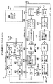
図2は、図1に示す本発明の一実施形態を非常に簡略化したブロック図であり、そこでは、ベースバンド・プロセッサ12は、以下に詳細に説明するような高速フーリエ変換回路28を含む。この図は、FFT回路を使用することができる無線1、無線2、及びイメージャーの、3つの可能な信号源を示しているが、このような信号源は単に例示的なものである。起動信号29、30、又は31が切替装置32に送られると、FFT回路28が、現在作動中のそれぞれの信号源に接続される。FFT回路28は、図1のDSPコア27の一部分としてもよいし、図2に示すように、バスに接続してもよい。
【0019】
これまで説明してきたように、RFトランシーバ10、11と自動ID読取装置の回路17は、共通のベースバンド・プロセッサ12を共用する。プロセッサ12の種々の態様を、ディジタル回路、又はコンピュータのハードウェア、ファームウェア、ソフトウェア、或いはこれらの組み合わせで実行することができる。本発明の装置は、プログラム可能なプロセッサによる実行のための機械読み取り可能な記憶デバイスの中に、又はメモリに取り込まれたソフトウェアに有形的に組み込まれたコンピュータ製品に実装することができる。プロセッサ12用には単一のASICが好ましいが、前述の技術は、例えば、入力データで作動し出力を生成することにより本発明の機能を実行するために、命令の一連の信号又はプログラムを実行可能な単一のマイクロプロセッサ、マルチプロセッサ、1つ又はそれ以上のディジタル信号プロセッサ、論理ゲートのゲートアレイ、又は配線結合された論理回路により実行することができる。この方法は、データ記憶システムからデータと命令を受信し、該データ記憶システムにデータと命令を送信するよう該データ記憶システムに接続された、少なくとも1つのプログラム可能なディジタル信号プロセッサと、少なくとも1つの入力装置と、少なくとも1つの出力装置を含むプログラム可能なシステム上で実行可能な、1つ又はそれ以上のコンピュータ・プログラムにおいて有利に実行することができる。各々のコンピュータ・プログラムは、高級な手続き型又はオブジェクト指向のプログラミング言語、或いは必要に応じて、アセンブリ言語又は機械言語で実行することが可能であり、どの場合においても、その言語は、コンパイラ型言語とすることもできるし、インタープリタ型言語とすることもできる。適当なプロセッサは、例えば、ディジタル信号プロセッサ、又は多目的及び特殊目的マイクロプロセッサの両方を含む。一般に、プロセッサは、読み取り専用メモリ及び/又はランダム・アクセス・メモリから命令とデータを受け取る。コンピュータ・プログラム命令とデータを有形的に組み込むのに適した記憶装置は、全ての形態の不揮発性メモリを含み、例えば、EPROM、EEPROM、及びフラッシュメモリ・デバイスのような半導体デバイスと、内蔵ハードディスク及び取り外し可能なディスクのような磁気ディスクと、光磁気ディスクと、CD−ROMディスクを含む。前述のいずれのものも、特定用途向け集積回路(ASIC)により補うこともできるし、その中に組み込むこともできる。
【0020】
図3に示されているように、参照番号300は、前述のSE1200レーザ・走査・エンジン・モジュールのような共通支持体を全体的に表しており、その上に、2重RFトランシーバと自動ID読取装置が支持される。この支持体は、ほぼ平坦な底部301と、該底部にほぼ平行で、該底部に対して上方に位置する平面に取り付けられたプリント基板302を含む。参照番号303で示される領域において、モジュール内部に自動ID読取装置(図示せず)が実装される。
【0021】
図4は、第1RFサブアセンブリと、それに対応する直交周波数分割多重方式(OFDM)無線を示すベースバンド回路の一例を表している。IEEE802.11a規格は、5GHzの帯域で動作するPHY層を指定しており、米国においてはデータを変調するための直交周波数分割多重技術に基づく無認可の装置に門戸が開放されている。OFDMにおいては、ディジタル・データは、多数の隣接するキャリアの中で分散されるため、比較的少量のデータのみが各々のキャリアで搬送される。隣接するキャリアは、数学的に直交している。隣接するキャリアの側波帯は重複することがあるが、隣接するキャリアに干渉されることなく信号を受信することができる。OFDM変調の主な利点は、屋内環境及びモバイル環境において直面するマルチパス・エコーに強いことである。
【0022】
IEEE802.11a規格では、各々のOFDMシンボルは、52個のノンゼロの副搬送波から構成され、そのうちの48個はデータ副搬送波であり、残り4個はキャリア・パイロット副搬送波である。そのデータ転送速度は、6Mbit/sから54Mbit/sまでの範囲内であり、隣接するチャネルの間隔は20MHZである。全ての実行には、6、12、及び24Mbit/sをサポートすることが必要とされる。オプションとしての拡張は、9、18、36、48、及び54Mbit/sである。データ転送速度の範囲は、屋内環境及び屋外環境の両方における広範囲の無線チャネル特性に適合するように与えられる。IEEE802.11のMACプロトコルのマルチレート機構は、IEEE802.11aのPHYと共に使用され、全ての装置が現在のチャネルにおける最高のデータ転送速度で互いに通信することを保障する。
【0023】
従来の単一搬送波ディジタル通信システムでは、データシンボルは、何らかの変調方式を用いてシリアル伝送され、各シンボルのスペクトルは、チャネル帯域幅全体を占有する。マルチキャリア変調方式では、データシンボルは、幾つかの形式の周波数分割多重化(FDM)により、チャネル帯域幅を共用する多数の副搬送波で並列に伝送される。或る副搬送波についての変調方式を、他の副搬送波に用いる変調方式と無関係に選択することができる。したがって、チャネルの周波数セグメントにおける、高い信号対雑音比(SNR)を有する副搬送波に、高速変調を使用することができ、その一方で、低いSNRを有する副搬送波には、低速変調を使用するか、又は変調しない。
【0024】
OFDMでは、副搬送波同士のスペクトルが重複しており、それらの間隔は、副搬送波の各々が他の全ての副搬送波に対して直交するよう選択される。副搬送波の直交性を得るための一般的な方法は、副搬送波シンボルの継続時間の逆数に等しい副搬送波の周波数間隔を選択することである。次に、並列データ・ブロックをそれぞれ変調及び復調する逆高速フーリエ変換(IFFT)及び高速フーリエ変換(FFT)として実行される離散フーリエ変換によって、OFDM信号のベースバンド処理が有効に行われる。1回の変換の間に生成された副搬送波の組は、1つのOFDMシンボルを定義する。副搬送波は、IFFTによって生成された時間サンプルのチャネル上をシリアル伝送により搬送される。OFDMシンボルの継続時間は、副搬送波シンボルの継続時間と同じであり、ゆえに、変換の時間窓と等しい。
【0025】
このようなシステムの1つを説明するために、米国特許第5,838,734号を引用によりここに組み込む。この特許では、送信器で最初に符号化されたキャリアの各々のI値及びQ値の出力に関するFFTが開示される。これらのI値及びQ値は、これらが表されている直交振幅変調(QAM)の位相図から各ベクトルに対する大きさZを導き出す変換器に送られる。これらのI値及びQ値はまた、QAM位相図における各ベクトルに対する角度を導き出し、これを位相誤差解析器と位相誤差補償器に供給する変換器に送られる。位相誤差解析器は、局部発振器に起因する位相ノイズを除去し、次いで位相誤差補償器において位相角度が補正され、補正された出力が与えられる。
【0026】
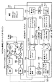
より詳細には、図4に、受信/送信スイッチ401に接続されたアンテナ(5GHz WLANと表記される)が示されている。受信側では、スイッチ401はLNA402に接続される。LNA402の出力は、乗算器403に接続される。乗算器403の出力は、フィルタ405に接続される。フィルタ405の出力は、アナログ・ディジタル変換器ADC406に接続され、該ADC406は、複合(IQ)復調及びタイミング同期回路407に接続される。複合(IQ)復調及びタイミング同期回路407の出力は、保護インターバル除去回路408に接続され、該保護インターバル除去回路408は、FFT409に接続される。FFT409の出力は、周波数ドメイン等化及びチャネル見積もり回路410に接続され、その出力は逆マッピング及び逆インターリービング回路411に接続される。逆マッピング及び逆インターリービング回路の出力は、ビタビ復号回路412に接続され、該ビタビ復号回路412の出力は、FIFO413に接続される。FIFO413は、MACプロトコル・スタック・プロセッサ414に接続される。
【0027】
プロトコル・スタック・プロセッサ414の出力は、FIFO413に戻るよう接続され、該FIFO413の出力は、畳込み符号器415に接続される。畳込み符号器415の出力は、シンボル・インターリービング及びI/Qマッピング416に接続される。416の出力は、パイロット挿入417に接続され、417の出力は、IFFT418に接続される。IFFT418は、保護インターバル挿入及びウィンドウ回路419に接続し、419の出力は、複合(IQ)変調回路420に接続される。
【0028】
最終的に、複合(IQ)変調回路420は、ディジタル・アナログ変換器DAC421における、ブロードバンドRFトランシーバ・システムに接続される。DAC421の出力は、フィルタ422に接続され、該フィルタ422の出力は、乗算器423に接続される。乗算器423の出力は、電力増幅器424に接続され、該電力増幅器424は、アンテナ(5GHzWLAN)に接続される。
【0029】
より詳細には、図5において、アンテナ(2GHzWWANと表記されている)が、501で示される受信/送信スイッチに接続される。受信側では、スイッチ501が、LNA502に接続される。LNA502の出力は、乗算器503に接続され、該乗算器503の出力は、フィルタ505に接続される。フィルタ505は、ADC506に接続される。
【0030】
ADC506の出力は、複合(IQ)復調及びタイミング同期回路507において、WCDMAベースバンドICに接続され、507の出力は、複合逆スクランブル回路508に接続される。回路508は、乗算器509に接続され、該乗算器509の出力は、チャネル見積もり及び等化回路510に接続される。回路510は、逆マッピング及び逆インターリービング回路511に接続され、回路511の出力は、ターボ・デコード回路512に接続される。回路512に接続されるのがFIFO513で、該FIFO513は、MAC・プロトコル・スタック・プロセッサ514に接続される。
【0031】
プロトコル・スタック・プロセッサ514の出力は、FIFO513に戻るよう接続され、該FIFO513の出力は、畳込み符号器515に接続される。符号器は、シンボル・インターリービング及びI/Qマッピング回路516に接続され、該回路516の出力は、256チップのウオルシュ・コード・ジェネレータ517と乗算器518の両方に接続される。518の出力は、複合スクランブリング回路519に接続され、該回路519の出力は、次に複合(IQ)変調回路520に接続される。
【0032】
最終的に、複合(IQ)変調回路520は、DAC521においてブロードバンドRFトランシーバ・システムに接続される。DAC521の出力は、フィルタ522に接続され、該フィルタ522の出力は、乗算器523に接続される。乗算器523の出力は、電力増幅器524に接続され、該電力増幅器524は、アンテナ(2GHzWWAN)に接続される。
【0033】
図6は、図4のOFDMトランシーバにおける逆高速フーリエ変換の実行の略図である。より詳細には、処理モジュール601は、一連の乗算器602、603、604を含み、これらは入力シンボルC0、C1、・・・CN-1に、図により詳細に示された指数因子を掛けるように動作する。結果として得られた積は、次いでユニット605で合計され、その出力は、乗算器606に入力され、そこで該出力にキャリア信号が乗算される。参考のためにIFFTプロセスを表す式も図中に示す。
【0034】
図7は、WCDMAトランシーバに使用されることがあるレーキ受信機/等化器の実行の略図である。レーキ受信機は、R.プライスらによるProc.IRE46,555−570(1958)により知られており、複数のマルチパス伝播経路のための復調構造を代表するものである。各マルチパス・コンポーネントの復調は、レーキの「フィンガー」である。この復調は、乗算器702、703、704、・・・と加算器705を用いてチャネル・インパルス応答見積もりg1、g2、g3、…を乗算することにより、加重され、位相調整され、遅延調整された符号語コンポーネントの和を生成する。
【0035】
自動ID読取装置は、好ましくは、半導体センサ又はCCDイメージャーであり、レーザ・走査・エンジン・サブアセンブリとすることもでき、また、レーザ・ビームを放射するためのレーザ・ダイオードと、レーザ・ビームを合焦するためのレンズと、該ビームをモジュールの外側に反射させるための走査ミラーと、該走査ミラーを動かし、バーコード・シンボルを横切るように光線を走らせ、バーコードから反射させるための駆動機構と、反射した光を検出するためのフォトダイオードと、反射した光を集め、それをフォトダイオードに導くための集光ミラーと、光学的な集光部品と、を含むことができる。フォトダイオードで生じる検出された信号を処理してディジタル化するために、ベースバンド・プロセッサ12への出力に、インターフェース18を接続することができる。
【0036】
前述の要素の各々、或いは2つ又はそれ以上は、前述の形式とは異なる他の形式の構造においても有効に利用できることが理解されるであろう。
【0037】
本発明について、モジュールにおける自動ID読取装置と単式又は2重無線周波数トランシーバに使用されるICを具現化して図示し、説明してきたが、これは、本発明が示された詳細に限定されることを意図するものではなく、本発明の精神から少しも逸脱することなしに種々の改良及び構造上の変更が可能である。
【0038】
これ以上分析しなくとも、前述したことは、本発明の要旨を十分に示しているであろうから、第三者は、現行の知識を応用することにより、従来技術の観点から見て本発明の一般的な態様又は特定の態様の本質的な特性を十分に構成する特徴を省略することなしに、本発明を種々の用途に容易に適合させることが可能であり、それゆえ、そのような適合は、付属の特許請求の範囲の均等物の意義及び範囲の中に包含されるべきであり、かつ、包含されることを意図するものである。
【図面の簡単な説明】
【図1】本発明に係る単一のICベースバンド・プロセッサ回路と共に2重RFトランシーバと自動ID読取装置回路を示すブロック図である。
【図2】単一のFFT回路が2重RFトランシーバの各々によって使用される状態を示す、本発明の一実施形態のブロック図である。
【図3】図1の回路を支持するためのモジュールを前方と下方から見た斜視図である。
【図4】本発明において使用されるOFDM RFトランシーバのブロック図である。
【図5】本発明において使用されるWCDMA RFトランシーバのブロック図である。
【図6】図4のトランシーバで使用される回路の略図である。
【図7】図5のトランシーバで使用できるように本発明により改良された図6の回路の略図である。
【符号の説明】
10 第1RFサブアセンブリ
11 第2RFサブアセンブリ
12 信号プロセッサ
13 バス
14 プロセッサ
15 メモリ
16 インターフェース
17 イメージャー
18 インターフェース
21 アンテナ
25 無線インターフェース
26 無線インターフェース
27 DSPコア
28 高速フーリエ変換回路
29 起動信号
32 切替装置
100 モジュール[0001]
BACKGROUND OF THE INVENTION
The present invention generally uses a mobile computer and a module or card for RF communication for use with such a computer and a baseband processor circuit for such a module, with the circuit in each radio 2 Small and compact due to heavy use In a rectangular space The present invention relates to a method for providing multiple radio capability.
[0002]
[Prior art]
Wireless networks use infrared or radio frequency communication channels to communicate between portable or mobile computer terminals and fixed access points or base stations. These access points are connected to the network infrastructure by a wired (or possibly wireless) communication channel, which connects groups of access points to each other, Form a local area network or wide area network optionally including further servers or host computer systems or gateways to the public switched telephone network.
[0003]
Radio protocols and radio frequency (RF) protocols are known that support the logical interconnection of portable roaming terminals with various types of communication capabilities to a host computer. The logical interconnect is based on an infrastructure that, when located within a predetermined range from an access point, at least some of each remote terminal can communicate with at least two of the access points Typically, each of the terminal devices is in communication with one of such access points. Based on total space coverage and location, response time, and network loading requirements, so that communication between a given terminal and the network via a selected access point can be most efficiently coordinated, Different modulation schemes, power limits, and communication protocols have been designed. One such protocol for local area networks is the “Wireless LAN / Media Access Control (MAC) and Physical Layer (PHY) specification available from ISO / IEC 8802-11, or the IEEE Standards Bureau in Piscataway, NJ. "(1999 edition) is described in the ANSI / IEEE 802.11 standard (hereinafter referred to as" IEEE 802.11 standard "), and another in the personal communication service area is the wide area network standard ( WCDMA).
[0004]
One form of mobile computer terminal connected to or incorporating a bar code symbol reader is currently very common for data collection applications. Typically, a barcode symbol is composed of one or more rows of light and dark regions, usually in the shape of a rectangle. The relative width of the dark areas or bars and / or the width of the spaces between the bright areas or bars encodes the data or information in the symbol.
[0005]
Bar code symbol readers illuminate the symbols and sense light reflected from regions of different light reflectivity to detect the relative width and spacing of each region and extract the encoded information. Bar code reading type data entry systems improve the efficiency and accuracy of data entry for various applications. The ease of data entry in such a system makes it easier to enter more detailed data more frequently, for example, making inventory inventory or tracking work in progress efficiently. It becomes like this.
[0006]
Various bar code readers and scanning systems are known. One particularly advantageous type of reader is an optical scanner that scans a beam of light, such as a laser beam, across a symbol. A moving beam laser scanner system and components of that type are typically shown in U.S. Pat. Nos. 4,387,297 and 4,760,248 owned by the assignee of the present invention. Incorporated here. Moving beam laser scanners are not the only form of optical device that can read symbols. Another type of reader called an “imager” is a type that incorporates a two-dimensional semiconductor sensor or linear charge coupled device (CCD) technology. Light is projected onto the entire symbol from a light source, such as a light emitting diode (LED) of the scanning device, and each pixel or CCD cell is read sequentially to determine, for example, whether a bar or space exists. As an example of a CCD reader, US patent application Ser. No. 09 / 096,578 filed June 12, 1998 by Correa et al. Is incorporated herein by reference.
[0007]
In the automatic recognition and data collection (AIDC) industry, certain types Built in a rectangular space Modules, ie specific space allocation assemblies or devices with known functionality, have become standard. A PC card or compact flash card is one such example in the portable computer industry. Another such bar code reader laser, scanning engine module known as "SE1200" Rectangular space Is manufactured by Symbol Technologies, Inc. of Holtsville, New York, which is employed in the AIDC industry and is the assignee of the present application. The SE1200 module is used in a handheld portable computer for reading bar code symbols and has a parallelepiped shape of 1 to 1/2 inch in length, 1 inch in width, and 3/4 inch in height.
[0008]
[Problems to be solved by the invention]
1. Object of the present invention
Accordingly, the general object of the present invention is to provide a single integrated circuit for use with two separate RF transceivers and optionally equipped automatic ID readers, all of which are common. Standards for use on supports, especially mobile computers In a rectangular space Attached to.
Another object of the present invention is to provide a module that uses a common baseband digital signal processing circuit for an automatic ID reader and a wireless transceiver.
[0009]
[Means for Solving the Problems]
2. Features of the present invention
Briefly stated in light of the above objectives and other objectives which will become apparent hereinafter, one of the features of the present invention is that of a given Define the rectangular space A dual radio frequency (RF) transceiver supported together on a common support and an automatic ID reader.
Each RF transceiver operates to communicate with a computer network through a different communication channel such as a wireless LAN or WAN, GPRS, CDPD, GSM cellular network, etc. The automatic ID reader operates to detect encoded data on a label or card, such as an identification card, and to image and / or read the encoded data of bar code symbols.
[0010]
In one preferred embodiment, the RF transceiver and automatic ID reader electrical components are mounted on a printed circuit board supported by the module. These components generate digital signals corresponding to the RF signal data and the encoded data. A single ASIC is supported on the module, receives and processes these digital signals, and outputs the processed signals to the host computer via a common interface.
[0011]
The novel features believed characteristic of the invention are set forth with particularity in the appended claims. However, the present invention itself is best understood with regard to its structure and its method of operation, and with respect to its additional objects and advantages, when reading the following description of specific embodiments in conjunction with the accompanying drawings. Will be understood.
[0012]
DETAILED DESCRIPTION OF THE INVENTION
Details including exemplary aspects and embodiments of the invention will now be described. Referring to the drawings,
[0013]
[0014]
[0015]
The
[0016]
The base station emits an RF signal that is detected by each radio antenna 21 or 23 in the module. In order to give the antenna dispersibility, it is also possible to arrange the second antenna 22 or 24 in each wireless system in the module. Here, when referring to “antenna”, the antennas 21, 22, 23, Any one of 24. The received RF signal is routed to a radio transceiver 11 that performs RF demodulation for communication protocol synchronization or acknowledgment, where an analog baseband signal counters the amplifier, bandpass filter, and received signal. A multiplier for sampling at a rate controlled by the signal generator to generate a sample signal, a peak detector for measuring the peak magnitude and duration of the sample signal, an automatic gain controller, and an analog sample signal And a digitizer for converting the signal into a digital signal. The digital signal is then routed through a connector or bus 13 to a host computer unit that includes a central processing unit (CPU) 14 for processing according to a stored algorithm. A memory 15 is connected to the CPU for storing and retrieving data. The output signal from the CPU is then routed through the
[0017]
Reference numeral 17 generally indicates a circuit of an automatic ID reader (shown as a semiconductor imager or CCD imager), which has at least one sensor and is connected to the
[0018]
FIG. 2 is a highly simplified block diagram of one embodiment of the present invention shown in FIG. 1, wherein the
[0019]
As described so far, the
[0020]
As shown in FIG. 3,
[0021]
FIG. 4 illustrates an example of a baseband circuit illustrating a first RF subassembly and a corresponding orthogonal frequency division multiplexing (OFDM) radio. The IEEE 802.11a standard specifies a PHY layer that operates in the 5 GHz band, and is open to unauthorized devices in the United States based on orthogonal frequency division multiplexing technology for modulating data. In OFDM, digital data is distributed among a number of adjacent carriers, so only a relatively small amount of data is carried on each carrier. Adjacent carriers are mathematically orthogonal. Although sidebands of adjacent carriers may overlap, signals can be received without being interfered by adjacent carriers. The main advantage of OFDM modulation is that it is resistant to multipath echoes encountered in indoor and mobile environments.
[0022]
In the IEEE 802.11a standard, each OFDM symbol is composed of 52 non-zero subcarriers, 48 of which are data subcarriers and the remaining 4 are carrier pilot subcarriers. The data transfer rate is in the range from 6 Mbit / s to 54 Mbit / s, and the interval between adjacent channels is 20 MHZ. All executions are required to support 6, 12, and 24 Mbit / s. Optional extensions are 9, 18, 36, 48, and 54 Mbit / s. A range of data rates is provided to suit a wide range of wireless channel characteristics in both indoor and outdoor environments. The multi-rate mechanism of the IEEE 802.11 MAC protocol is used in conjunction with the IEEE 802.11a PHY to ensure that all devices communicate with each other at the highest data rate on the current channel.
[0023]
In conventional single carrier digital communication systems, data symbols are serially transmitted using some modulation scheme, and the spectrum of each symbol occupies the entire channel bandwidth. In multi-carrier modulation schemes, data symbols are transmitted in parallel on multiple subcarriers sharing channel bandwidth by some form of frequency division multiplexing (FDM). The modulation scheme for a certain subcarrier can be selected independently of the modulation scheme used for other subcarriers. Therefore, fast modulation can be used for sub-carriers with high signal-to-noise ratio (SNR) in the frequency segment of the channel, while low-speed modulation is used for sub-carriers with low SNR. Or do not modulate.
[0024]
In OFDM, the spectrum of subcarriers overlaps and their spacing is selected so that each subcarrier is orthogonal to all other subcarriers. A common way to obtain subcarrier orthogonality is to select a subcarrier frequency interval equal to the inverse of the subcarrier symbol duration. Next, baseband processing of the OFDM signal is effectively performed by discrete Fourier transforms implemented as inverse fast Fourier transform (IFFT) and fast Fourier transform (FFT), which modulate and demodulate the parallel data blocks, respectively. The set of subcarriers generated during one conversion defines one OFDM symbol. The subcarrier is carried by serial transmission over a channel of time samples generated by IFFT. The duration of the OFDM symbol is the same as the duration of the subcarrier symbol and is therefore equal to the time window of the conversion.
[0025]
To illustrate one such system, US Pat. No. 5,838,734 is incorporated herein by reference. In this patent, an FFT for the output of the I and Q values of each of the first encoded carriers at the transmitter is disclosed. These I and Q values are sent to a converter that derives the magnitude Z for each vector from the quadrature amplitude modulation (QAM) phase diagram in which they are represented. These I and Q values are also sent to a converter that derives an angle for each vector in the QAM phase diagram and supplies it to the phase error analyzer and phase error compensator. The phase error analyzer removes the phase noise due to the local oscillator, and then the phase angle is corrected in the phase error compensator to provide a corrected output.
[0026]
More specifically, FIG. 4 shows an antenna (denoted as 5 GHz WLAN) connected to the reception /
[0027]
The output of
[0028]
Finally, the composite (IQ)
[0029]
More specifically, in FIG. 5, an antenna (denoted as 2 GHz WWAN) is connected to a receive / transmit switch indicated at 501. On the receiving side, the
[0030]
The output of the
[0031]
The output of
[0032]
Finally, the composite (IQ)
[0033]
FIG. 6 is a schematic diagram of performing an inverse fast Fourier transform in the OFDM transceiver of FIG. More specifically, the
[0034]
FIG. 7 is a schematic diagram of an implementation of a rake receiver / equalizer that may be used in a WCDMA transceiver. The rake receiver is R.D. Price et al., Proc. IRE 46, 555-570 (1958), which represents a demodulation structure for multiple multipath propagation paths. The demodulation of each multipath component is a rake “finger”. This demodulation is performed by using a
[0035]
The automatic ID reader is preferably a semiconductor sensor or CCD imager, which may be a laser scanning engine subassembly, a laser diode for emitting a laser beam, and a laser beam. A lens for focusing, a scanning mirror for reflecting the beam to the outside of the module, and a drive for moving the scanning mirror to run the light beam across the barcode symbol and reflect it from the barcode A mechanism, a photodiode for detecting the reflected light, a collection mirror for collecting the reflected light and directing it to the photodiode, and an optical collection component can be included. An
[0036]
It will be appreciated that each or two or more of the aforementioned elements may be effectively utilized in other types of structures that are different from the foregoing types.
[0037]
Although the invention has been illustrated and described with respect to an IC used in an automatic ID reader and a single or dual radio frequency transceiver in a module, this is limited to the details shown. However, various modifications and structural changes can be made without departing from the spirit of the present invention.
[0038]
Even without further analysis, the above will fully show the gist of the present invention, so that third parties can apply the current knowledge to view the present invention from the viewpoint of the prior art. It is possible to easily adapt the present invention to various applications without omitting features that sufficiently constitute the essential characteristics of the general aspect or specific aspect of the invention. Such adaptations are and are intended to be encompassed within the meaning and scope of equivalents of the appended claims.
[Brief description of the drawings]
FIG. 1 is a block diagram illustrating a dual RF transceiver and automatic ID reader circuit with a single IC baseband processor circuit in accordance with the present invention.
FIG. 2 is a block diagram of one embodiment of the present invention showing a single FFT circuit being used by each of the dual RF transceivers.
FIG. 3 is a perspective view of a module for supporting the circuit of FIG. 1 as viewed from the front and the bottom.
FIG. 4 is a block diagram of an OFDM RF transceiver used in the present invention.
FIG. 5 is a block diagram of a WCDMA RF transceiver used in the present invention.
6 is a schematic diagram of circuitry used in the transceiver of FIG.
7 is a schematic diagram of the circuit of FIG. 6 modified according to the present invention for use with the transceiver of FIG.
[Explanation of symbols]
10 First RF subassembly
11 Second RF subassembly
12 Signal processor
13 Bus
14 processor
15 memory
16 interface
17 Imager
18 interface
21 Antenna
25 Wireless interface
26 Wireless interface
27 DSP core
28 Fast Fourier Transform Circuit
29 Start signal
32 switching device
100 modules
Claims (15)
b)前記支持体に支持され、第1通信規格に従ってデータを送信するよう作動する第1無線周波数(RF)トランシーバと、
c)前記支持体に支持され、前記第1規格とは異なる第2通信規格に従ってデータを送信するよう作動する第2無線周波数(RF)トランシーバと、
d)前記支持体に支持され、前記第1及び第2RFトランシーバに接続され、前記RFトランシーバの各々のベースバンド信号を処理する共通ベースバンド・プロセッサと、
e)少なくとも1つのセンサを有し、前記支持体に支持され、インタフェース回路を介して前記ベースバンド・プロセッサに接続された自動ID読取装置と、
を備え、
f)前記自動ID読取装置は、読み取るシンボルを照明し、該記号により反射された光を受けて該シンボルの読み取りを行うものであり、
g)前記第1無線周波数(RF)トランシーバと前記第2無線周波数(RF)トランシーバのうち、送信先が利用できる通信規格に対応する通信規格をもった方のトランシーバを通じて、前記自動ID読取装置により読み取られた前記シンボルのデータを送信する
ことを特徴とするRF通信用モジュール。a) a support that defines a predetermined rectangular space;
b) a first radio frequency (RF) transceiver supported on the support and operative to transmit data in accordance with a first communication standard;
c) a second radio frequency (RF) transceiver supported by the support and operable to transmit data in accordance with a second communication standard different from the first standard;
d) a common baseband processor supported by the support and connected to the first and second RF transceivers and processing a baseband signal of each of the RF transceivers;
e) an automatic ID reader having at least one sensor, supported by the support and connected to the baseband processor via an interface circuit;
Equipped with a,
f) The automatic ID reader illuminates a symbol to be read, receives the light reflected by the symbol, and reads the symbol;
g) by means of the automatic ID reader through the transceiver having the communication standard corresponding to the communication standard available to the transmission destination of the first radio frequency (RF) transceiver and the second radio frequency (RF) transceiver. Transmit the data of the read symbol
An RF communication module.
b)前記ハウジングに支持され、所定の長方体形状のスペースを定める支持体と、
c)前記支持体に支持され、第1及び第2コンピュータ・ネットワークにそれぞれ関連する第1及び第2RF基地局と通信して、端末とネットワークとの間でデータ転送するように動作する第1及び第2無線周波数(RF)トランシーバと、
d)前記支持体に支持され、バーコード記号を照明して該バーコード記号から反射された光を感知して前記バーコード記号の読み取りを行うように作動する自動読取装置と、
を備え、
e)前記第1及び前記第2無線周波数(RF)トランシーバのうち、送信先が利用できる通信規格に対応する通信規格をもった方のトランシーバを通じて、前記自動ID読取装置により読み取られた前記シンボルのデータを送信する
ことを特徴とするモバイル・コンピュータ・収集端末。a) a hand-held housing;
b) a support which is supported by the housing and defines a predetermined rectangular space;
c) first and second supported by the support and in communication with first and second RF base stations associated with the first and second computer networks, respectively, to transfer data between the terminal and the network; A second radio frequency (RF) transceiver;
d) an automatic reader supported by the support and operative to illuminate a barcode symbol and sense light reflected from the barcode symbol to read the barcode symbol ;
Equipped with a,
e) Of the first and second radio frequency (RF) transceivers, the symbol read by the automatic ID reader through a transceiver having a communication standard corresponding to a communication standard that can be used by a transmission destination. Send data
A mobile computer / collector terminal.
Applications Claiming Priority (2)
| Application Number | Priority Date | Filing Date | Title |
|---|---|---|---|
| US09/939861 | 2001-08-27 | ||
| US09/939,861 US6895219B2 (en) | 2001-08-27 | 2001-08-27 | Dual use of FFT circuity in imagers and transceivers |
Publications (3)
| Publication Number | Publication Date |
|---|---|
| JP2003087148A JP2003087148A (en) | 2003-03-20 |
| JP2003087148A5 JP2003087148A5 (en) | 2005-09-15 |
| JP4312414B2 true JP4312414B2 (en) | 2009-08-12 |
Family
ID=25473859
Family Applications (1)
| Application Number | Title | Priority Date | Filing Date |
|---|---|---|---|
| JP2002116423A Expired - Lifetime JP4312414B2 (en) | 2001-08-27 | 2002-04-18 | Double use of FFT circuit by imager and transceiver |
Country Status (5)
| Country | Link |
|---|---|
| US (1) | US6895219B2 (en) |
| JP (1) | JP4312414B2 (en) |
| DE (1) | DE10211923B4 (en) |
| FR (1) | FR2828952B1 (en) |
| GB (1) | GB2379363B (en) |
Cited By (1)
| Publication number | Priority date | Publication date | Assignee | Title |
|---|---|---|---|---|
| CN102240166B (en) * | 2011-05-20 | 2013-12-18 | 陈茂强 | Double-layer vacuum-type electric heating water boiling thermos bottle |
Families Citing this family (34)
| Publication number | Priority date | Publication date | Assignee | Title |
|---|---|---|---|---|
| US7386326B2 (en) * | 2001-09-04 | 2008-06-10 | Texas Instruments Incorporated | Programmable task-based co-processor |
| AU2002327681A1 (en) * | 2001-09-24 | 2003-04-07 | Atheros Communications, Inc. | Method and system for variable rate acknowledgement for wireless communication protocols |
| US7421291B2 (en) * | 2002-08-12 | 2008-09-02 | Broadcom Corporation | Method for selective power management for a hand held host |
| US7266389B2 (en) * | 2002-08-12 | 2007-09-04 | Broadcom Corporation | Device for selective power management for a hand held host |
| US7762460B2 (en) | 2004-02-18 | 2010-07-27 | Nec Corporation | Information processing device for using bar code and radio frequency-identification tag |
| US20050226345A1 (en) * | 2004-03-31 | 2005-10-13 | Interdigital Technology Corporation | Apparatus for reducing channel interference between proximate wireless communication units |
| US20060089174A1 (en) * | 2004-04-29 | 2006-04-27 | Tapwave, Inc. | Mobile computing device with a physical button for wireless communications |
| KR100585152B1 (en) * | 2004-08-02 | 2006-05-30 | 삼성전자주식회사 | Wireless OFDM-based modem using TX time-domain equalizer and data transmission method thereof |
| US7804906B2 (en) * | 2004-11-01 | 2010-09-28 | Metanoia Technologies, Inc. | Multicarrier transceiver |
| US20060128331A1 (en) * | 2004-12-13 | 2006-06-15 | Rooyen Pieter V | Method and system for mobile architecture supporting cellular or wireless networks and broadcast utilizing a single chip cellular and single chip broadcast silicon solution |
| EP4216103A1 (en) * | 2005-03-11 | 2023-07-26 | Hand Held Products, Inc. | Bar code reading device with global electronic shutter control |
| US7568628B2 (en) | 2005-03-11 | 2009-08-04 | Hand Held Products, Inc. | Bar code reading device with global electronic shutter control |
| US7770799B2 (en) | 2005-06-03 | 2010-08-10 | Hand Held Products, Inc. | Optical reader having reduced specular reflection read failures |
| US8139672B2 (en) * | 2005-09-23 | 2012-03-20 | Qualcomm Incorporated | Method and apparatus for pilot communication in a multi-antenna wireless communication system |
| EP1964029B1 (en) * | 2005-12-22 | 2011-07-20 | LG Innotek Co., Ltd. | Rfid system |
| KR100775214B1 (en) * | 2005-12-22 | 2007-11-12 | 엘지이노텍 주식회사 | RFID system |
| US7885668B2 (en) * | 2006-01-31 | 2011-02-08 | Microsoft Corporation | Determining the network location of a user device based on transmitter fingerprints |
| US8234536B1 (en) * | 2006-07-07 | 2012-07-31 | Aquantia Corporation | Iterative decoder using input data pipelining and time-interleaved processing |
| TWI333342B (en) * | 2006-11-06 | 2010-11-11 | Inst Information Industry | Signal relay apparatus, method, application program, and computer readable medium capable of adjusting amplifying gain dynamicaaly |
| CN100589369C (en) * | 2007-02-13 | 2010-02-10 | 中国科学院上海微系统与信息技术研究所 | Method for multi-user transmission in ultra-short wave OFDM mobile multimedia sensor network TDMA |
| WO2009105040A1 (en) * | 2008-02-19 | 2009-08-27 | Bilcare Technologies Singapore Pte. Ltd. | A reading device for identifying a tag or an object adapted to be identified, related methods and systems |
| US20100252631A1 (en) * | 2009-04-01 | 2010-10-07 | Infineon Technologies Ag | High speed contactless communication |
| EP2271019B1 (en) * | 2009-06-30 | 2014-08-06 | Vodafone Holding GmbH | Mobile communication system using adaptive compression |
| US9647623B2 (en) * | 2009-09-30 | 2017-05-09 | Silicon Laboratories Inc. | Signal processor suitable for low intermediate frequency (LIF) or zero intermediate frequency (ZIF) operation |
| US10863988B2 (en) | 2017-11-29 | 2020-12-15 | Intuitive Surgical Operations, Inc. | Surgical instrument with lockout mechanism |
| US11517312B2 (en) | 2018-02-12 | 2022-12-06 | Intuitive Surgical Operations, Inc. | Surgical instrument with lockout mechanism |
| EP4338687A2 (en) | 2018-02-26 | 2024-03-20 | Intuitive Surgical Operations, Inc. | Surgical instrument with lockout mechanism |
| EP3897404A4 (en) | 2018-12-21 | 2023-01-04 | Intuitive Surgical Operations, Inc. | Surgical instruments having a reinforced staple cartridge |
| US11857188B2 (en) | 2018-12-21 | 2024-01-02 | Intuitive Surgical Operations, Inc. | Articulation assemblies for surgical instruments |
| US11806015B2 (en) | 2018-12-21 | 2023-11-07 | Intuitive Surgical Operations, Inc. | Surgical instruments having mechanisms for identifying and/or deactivating stapler cartridges |
| WO2020214258A1 (en) | 2019-04-15 | 2020-10-22 | Intuitive Surgical Operations, Inc. | Staple cartridge for a surgical instrument |
| EP3975875A4 (en) | 2019-05-31 | 2023-02-01 | Intuitive Surgical Operations, Inc. | Staple cartridge for a surgical instrument |
| US11786325B2 (en) | 2019-07-02 | 2023-10-17 | Intuitive Surgical Operations, Inc. | Remotely controlling a system using video |
| US11642129B2 (en) | 2020-01-15 | 2023-05-09 | Intuitive Surgical Operations, Inc. | Staple cartridge and drive member for surgical instrument |
Family Cites Families (11)
| Publication number | Priority date | Publication date | Assignee | Title |
|---|---|---|---|---|
| US5834753A (en) | 1986-08-08 | 1998-11-10 | Norand Corporation | Laser scanner module having integral interface with hand-held data capture terminal proximity and label sensing, and enhanced sensitivity and power efficiency |
| US5710728A (en) | 1991-07-11 | 1998-01-20 | Norand Corporation | Portable work station-type data collection system |
| US6448926B1 (en) | 1993-11-19 | 2002-09-10 | Itt Manufacturing Enterprises, Inc. | Multi-band, multi-function integrated transceiver |
| US5640002A (en) | 1995-08-15 | 1997-06-17 | Ruppert; Jonathan Paul | Portable RF ID tag and barcode reader |
| EP0780993A3 (en) | 1995-12-21 | 2000-01-19 | Lucent Technologies Inc. | Radiotelephone transceiver operative over more than one frequency range |
| KR100201814B1 (en) | 1996-12-06 | 1999-06-15 | 윤종용 | Radio signal processing apparatus in multi mode portable phone |
| GB2320631B (en) | 1996-12-23 | 2001-07-18 | Nokia Mobile Phones Ltd | Radio receiver and radio transmitter |
| GB9921802D0 (en) | 1999-09-16 | 1999-11-17 | Roke Manor Research | Use of umts cellphones with inbuilt camera and image processing to interact with barcodes to allow new applications and new services |
| WO2001037437A2 (en) | 1999-11-15 | 2001-05-25 | Psion Connect Limited | Removable wireless device |
| US6264106B1 (en) | 1999-12-27 | 2001-07-24 | Symbol Technologies, Inc. | Combination bar code scanner/RFID circuit |
| US6761316B2 (en) * | 2001-03-27 | 2004-07-13 | Symbol Technologies, Inc. | Compact auto ID reader and radio frequency transceiver data collection module |
-
2001
- 2001-08-27 US US09/939,861 patent/US6895219B2/en not_active Expired - Lifetime
-
2002
- 2002-03-18 DE DE10211923.6A patent/DE10211923B4/en not_active Expired - Lifetime
- 2002-03-22 GB GB0206833A patent/GB2379363B/en not_active Expired - Lifetime
- 2002-04-18 JP JP2002116423A patent/JP4312414B2/en not_active Expired - Lifetime
- 2002-04-25 FR FR0205223A patent/FR2828952B1/en not_active Expired - Lifetime
Cited By (1)
| Publication number | Priority date | Publication date | Assignee | Title |
|---|---|---|---|---|
| CN102240166B (en) * | 2011-05-20 | 2013-12-18 | 陈茂强 | Double-layer vacuum-type electric heating water boiling thermos bottle |
Also Published As
| Publication number | Publication date |
|---|---|
| FR2828952B1 (en) | 2005-12-02 |
| DE10211923B4 (en) | 2018-03-22 |
| GB2379363B (en) | 2006-04-26 |
| GB0206833D0 (en) | 2002-05-01 |
| FR2828952A1 (en) | 2003-02-28 |
| DE10211923A1 (en) | 2003-03-20 |
| US6895219B2 (en) | 2005-05-17 |
| GB2379363A (en) | 2003-03-05 |
| US20030040275A1 (en) | 2003-02-27 |
| JP2003087148A (en) | 2003-03-20 |
Similar Documents
| Publication | Publication Date | Title |
|---|---|---|
| JP4312414B2 (en) | Double use of FFT circuit by imager and transceiver | |
| US7054296B1 (en) | Wireless local area network (WLAN) technology and applications including techniques of universal frequency translation | |
| US8451093B2 (en) | RFID tag, interrogator and system with improved symbol encoding and decoding | |
| US8451097B2 (en) | RFID interrogator with improved symbol decoding and methods based thereon | |
| US6761316B2 (en) | Compact auto ID reader and radio frequency transceiver data collection module | |
| EP2302561B1 (en) | Encoded information reading terminal with user-configurable multi-protocol wireless communication interface | |
| Kellogg et al. | Passive {Wi-Fi}: Bringing Low Power to {Wi-Fi} Transmissions | |
| US6501807B1 (en) | Data recovery system for radio frequency identification interrogator | |
| JP3438918B2 (en) | Wireless LAN | |
| US6754170B1 (en) | Timing synchronization in OFDM communications receivers | |
| De Donno et al. | Challenge: Towards distributed RFID sensing with software-defined radio | |
| EP0405074A2 (en) | Hand-held bar code scanner | |
| WO2002031988A2 (en) | Ultra wide bandwidth noise cancellation mechanism and method | |
| JP2003087148A5 (en) | ||
| CN1741514A (en) | Backscatter interrogator reception method and interrogator for a modulated backscatter system | |
| Guo et al. | Efficient ambient LoRa backscatter with on-off keying modulation | |
| CN101897125B (en) | Method and apparatus for detecting a frequency band and mode of operation | |
| Li et al. | Passive {DSSS}: Empowering the downlink communication for backscatter systems | |
| US6778519B1 (en) | Wireless multiple function PC card | |
| El-Hadidy et al. | A novel collision avoidance MAC protocol for multi-tag UWB chipless RFID systems based on notch position modulation | |
| CN102184376A (en) | Network-agnostic encoded information reading terminal | |
| CN101444129A (en) | Method and apparatus for communication system | |
| US6873835B2 (en) | Antenna selection circuit for use in mobile computers | |
| US8934355B2 (en) | Wireless communication with diversity control | |
| An et al. | Identifying UHF RFIDs in range of readers with WiFi |
Legal Events
| Date | Code | Title | Description |
|---|---|---|---|
| A521 | Request for written amendment filed |
Free format text: JAPANESE INTERMEDIATE CODE: A523 Effective date: 20050331 |
|
| A621 | Written request for application examination |
Free format text: JAPANESE INTERMEDIATE CODE: A621 Effective date: 20050331 |
|
| A131 | Notification of reasons for refusal |
Free format text: JAPANESE INTERMEDIATE CODE: A131 Effective date: 20080623 |
|
| A521 | Request for written amendment filed |
Free format text: JAPANESE INTERMEDIATE CODE: A523 Effective date: 20080922 |
|
| A131 | Notification of reasons for refusal |
Free format text: JAPANESE INTERMEDIATE CODE: A131 Effective date: 20081215 |
|
| A521 | Request for written amendment filed |
Free format text: JAPANESE INTERMEDIATE CODE: A523 Effective date: 20090313 |
|
| TRDD | Decision of grant or rejection written | ||
| A01 | Written decision to grant a patent or to grant a registration (utility model) |
Free format text: JAPANESE INTERMEDIATE CODE: A01 Effective date: 20090413 |
|
| A01 | Written decision to grant a patent or to grant a registration (utility model) |
Free format text: JAPANESE INTERMEDIATE CODE: A01 |
|
| A61 | First payment of annual fees (during grant procedure) |
Free format text: JAPANESE INTERMEDIATE CODE: A61 Effective date: 20090513 |
|
| FPAY | Renewal fee payment (event date is renewal date of database) |
Free format text: PAYMENT UNTIL: 20120522 Year of fee payment: 3 |
|
| R150 | Certificate of patent or registration of utility model |
Free format text: JAPANESE INTERMEDIATE CODE: R150 Ref document number: 4312414 Country of ref document: JP Free format text: JAPANESE INTERMEDIATE CODE: R150 |
|
| FPAY | Renewal fee payment (event date is renewal date of database) |
Free format text: PAYMENT UNTIL: 20130522 Year of fee payment: 4 |
|
| R250 | Receipt of annual fees |
Free format text: JAPANESE INTERMEDIATE CODE: R250 |
|
| FPAY | Renewal fee payment (event date is renewal date of database) |
Free format text: PAYMENT UNTIL: 20130522 Year of fee payment: 4 |
|
| R250 | Receipt of annual fees |
Free format text: JAPANESE INTERMEDIATE CODE: R250 |
|
| R250 | Receipt of annual fees |
Free format text: JAPANESE INTERMEDIATE CODE: R250 |
|
| R250 | Receipt of annual fees |
Free format text: JAPANESE INTERMEDIATE CODE: R250 |
|
| R250 | Receipt of annual fees |
Free format text: JAPANESE INTERMEDIATE CODE: R250 |
|
| R250 | Receipt of annual fees |
Free format text: JAPANESE INTERMEDIATE CODE: R250 |
|
| R250 | Receipt of annual fees |
Free format text: JAPANESE INTERMEDIATE CODE: R250 |
|
| R250 | Receipt of annual fees |
Free format text: JAPANESE INTERMEDIATE CODE: R250 |
|
| R250 | Receipt of annual fees |
Free format text: JAPANESE INTERMEDIATE CODE: R250 |
|
| R250 | Receipt of annual fees |
Free format text: JAPANESE INTERMEDIATE CODE: R250 |
|
| EXPY | Cancellation because of completion of term |