JP4309070B2 - Nonvolatile semiconductor memory device and manufacturing method thereof - Google Patents
Nonvolatile semiconductor memory device and manufacturing method thereof Download PDFInfo
- Publication number
- JP4309070B2 JP4309070B2 JP2001023973A JP2001023973A JP4309070B2 JP 4309070 B2 JP4309070 B2 JP 4309070B2 JP 2001023973 A JP2001023973 A JP 2001023973A JP 2001023973 A JP2001023973 A JP 2001023973A JP 4309070 B2 JP4309070 B2 JP 4309070B2
- Authority
- JP
- Japan
- Prior art keywords
- memory cell
- transistor
- diffusion layer
- insulating film
- gate electrode
- Prior art date
- Legal status (The legal status is an assumption and is not a legal conclusion. Google has not performed a legal analysis and makes no representation as to the accuracy of the status listed.)
- Expired - Fee Related
Links
Images


Landscapes
- Semiconductor Memories (AREA)
- Non-Volatile Memory (AREA)
Description
【0001】
【発明の属する技術分野】
この発明は、特に少なくとも1つのメモリセルトランジスタを含むメモリセルユニットと、このメモリセルユニットに接続された選択ゲートトランジスタとを具備する不揮発性半導体記憶装置およびその製造方法に関する。
【0002】
【従来の技術】
図28に、従来のNAND型半導体記憶装置における、メモリセルトランジスタ及び選択ゲートトランジスタのゲート長“L”方向の断面図を示す。
【0003】
選択ゲートトランジスタのゲート電極間には、これらゲート電極に対して自己整合的に形成されたコンタクト孔34が形成されている。メモリセルトランジスタのゲート側壁には、ホットキャリア特性を良くするため、TEOS膜29が堆積されている。
【0004】
一方、選択ゲートトランジスタは、コンタクト孔34開口の際に、TEOS膜29がエッチングされて、コンタクト埋め込み材とゲート電極がショートするのを防ぐために、コンタクト孔34を開口する前に、ゲート側壁のTEOS膜29を剥離した構造となっている。メモリセルトランジスタと選択ゲートトランジスタのチャネル領域及びソース/ドレイン拡散層領域28に対する不純物のイオン注入は同時に行われるため、チャネル領域及びソース/ドレイン拡散層領域28の不純物分布は、メモリセルトランジスタと選択ゲートトランジスタで同様になっている。
【0005】
NAND型半導体記憶装置では、メモリセルに“1”データを書き込む(浮遊ゲートに電子を注入せず、消去時のしきい値を保つ)際、そのメモリセルトランジスタに接続された選択ゲートトランジスタを介して、ビット線から初期電位を充電し、選択ワード線には書き込み電圧、非選択ワード線には転送電圧を印加し、容量結合を利用してメモリセルトランジスタのチャネル領域の電位を昇圧することにより、浮遊ゲート5、11に電子が注入されないようにしている。このため、チャネル領域の不純物濃度を下げることによりチャネル容量が低下し、チャネル領域の電位が昇圧されやすくなり、“1”データ書き込み特性が向上する。
【0006】
【発明が解決しようとする課題】
しかしながら、メモリセルトランジスタと選択ゲートトランジスタのチャネル領域の不純物分布が同じであるため、チャネル領域の不純物濃度を下げることによって、選択ゲートトランジスタのしきい値電圧が低下し、オフリーク電流が増加して、正常な動作ができなくなる事情があった。
【0007】
この発明は上記事情に鑑みて為されたもので、その目的は、データ書き込み特性、データ保持特性、読み出しストレスに対する耐性などのメモリセルトランジスタの様々な特性と、選択ゲートトランジスタのカットオフ特性とをともに良好にできる不揮発性半導体記憶装置およびその製造方法を提供することにある。
【0008】
【課題を解決するための手段】
上記目的を達成するために、この発明の第1の態様に係る不揮発性半導体記憶装置は、半導体基板上に形成された、電荷蓄積層と制御ゲート層との積層構造を有する、少なくとも1つのメモリセルトランジスタを含むメモリセルユニットと、ソース/ドレイン拡散層領域の一方がビット線またはソース線に接続され、他方が前記メモリセルユニットに接続された選択ゲートトランジスタとを具備し、前記選択ゲートトランジスタのゲート電極下で、この選択ゲートトランジスタのソース拡散層領域の形状とドレイン拡散層領域の形状とが非対称であり、前記半導体基板とゲート絶縁膜との界面からの深さが等しい位置で、前記ビット線またはソース線に接続された拡散層領域と前記ゲート電極とが重なり合う距離が、前記メモリセルユニットに接続された拡散層領域と前記ゲート電極とが重なり合う距離よりも小さく、前記ビット線またはソース線に接続された拡散層領域の実効的な不純物濃度が、前記メモリセルユニットに接続された拡散層領域の実効不純物濃度よりも薄く、前記メモリセルユニットに接続された拡散層領域の実効的な不純物濃度が、前記メモリセルトランジスタのソース/ドレイン拡散層領域の実効的な不純物濃度と同じであり、前記メモリセルトランジスタのゲート電極の側壁、及び前記選択ゲートトランジスタのゲート電極の前記メモリセルに対向する側には、第1の絶縁膜と、この第1の絶縁膜上に形成された第2の絶縁膜と、この第2の絶縁膜上に形成された第3の絶縁膜とが積層されており、前記選択ゲートトランジスタのゲート電極の、前記ビット線またはソース線を接続するためのコンタクトに対向する側には、前記第1の絶縁膜と、この第1の絶縁膜上に形成された前記第3の絶縁膜とが積層されていることを特徴としている。
【0009】
このような第1の態様に係る不揮発性半導体記憶装置によれば、選択ゲートトランジスタのソース拡散層領域とドレイン拡散層領域との形状を非対称としたことにより、選択ゲートトランジスタの実効ゲート長を長くすることができる。この結果、選択ゲートトランジスタのショートチャネル効果が改善され、そのカットオフ特性が向上する。さらに選択ゲートトランジスタのショートチャネル効果が改善されることから、メモリセルトランジスタのチャネル領域の不純物濃度は、従来以下に下げることも可能である。この結果、メモリセルトランジスタのデータ書き込み特性を向上できる。
【0010】
また、この発明の第2の態様に係る不揮発性半導体記憶装置は、半導体基板上に形成された、電荷蓄積層と制御ゲート層との積層構造を有する、少なくとも1つのメモリセルトランジスタを含むメモリセルユニットと、ソース/ドレイン拡散層領域の一方がビット線またはソース線に接続され、他方が前記メモリセルユニットに接続された選択ゲートトランジスタとを具備し、前記選択ゲートトランジスタのゲート電極下で、この選択ゲートトランジスタのソース拡散層領域の形状とドレイン拡散層領域の形状とが非対称であり、前記半導体基板とゲート絶縁膜との界面からの深さが等しい位置で、前記ビット線またはソース線に接続された拡散層領域と前記ゲート電極とが重なり合う距離が、前記メモリセルユニットに接続された拡散層領域と前記ゲート電極とが重なり合う距離よりも小さく、前記ビット線またはソース線に接続された拡散層領域に接するチャネル領域の不純物濃度が、前記メモリセルユニットに接続された拡散層領域に接するチャネル領域の不純物濃度よりも濃く、前記メモリセルユニットに接続された拡散層領域に接するチャネル領域の不純物濃度が、前記メモリセルトランジスタのソース/ドレイン拡散層領域に接するチャネル領域の不純物濃度と同じであり、前記メモリセルトランジスタのゲート電極の側壁、及び前記選択ゲートトランジスタのゲート電極の前記メモリセルに対向する側には、第1の絶縁膜と、この第1の絶縁膜上に形成された第2の絶縁膜と、この第2の絶縁膜上に形成された第3の絶縁膜とが積層されており、前記選択ゲートトランジスタのゲート電極の、前記ビット線またはソース線を接続するためのコンタクトに対向する側には、前記第1の絶縁膜と、この第1の絶縁膜上に形成された前記第3の絶縁膜とが積層されていることを特徴としている。
【0011】
このような第2の態様に係る不揮発性半導体記憶装置によれば、選択ゲートトランジスタのソース拡散層領域とドレイン拡散層領域との間のチャネル領域に、不純物濃度が異なる領域を有することにより、選択ゲートトランジスタの実効ゲート長を長くすることができる。よって、第1の態様に係る不揮発性半導体記憶装置と同様の効果を得ることができる。
【0014】
また、この発明の第3の態様に係る不揮発性半導体記憶装置の製造方法は、半導体基板上に、第1導電型のチャネル領域を有するメモリセルトランジスタ及び選択ゲートトランジスタのゲート電極を形成する工程と、前記メモリセルトランジスタ及び前記選択ゲートトランジスタのゲート電極の側壁に第1の絶縁膜を形成する工程と、前記第1の絶縁膜上に、第2の絶縁膜を形成する工程と、前記選択ゲートトランジスタのゲート電極の、前記メモリセルトランジスタに対向する側とは反対側に開口を持つマスクを形成する工程と、前記マスクの開口を介して前記第2の絶縁膜を除去する工程と、前記マスクの開口を介して前記選択ゲートトランジスタのゲート電極下に第1導電型の不純物を注入する工程と を具備することを特徴としている。
【0015】
このような第3の態様に係る不揮発性半導体記憶装置の製造方法によれば、選択ゲートトランジスタのゲート電極から第2の絶縁膜を除去するためのマスクを利用して、このマスクの開口を介してチャネル領域と同じ導電型の不純物を注入する。これにより、不純物注入のためのマスク形成工程を増加させることなく、即ち、製造コストの増加を伴うことなく、上記第1、第2の態様に係る不揮発性半導体記憶装置を製造することができる。
【0018】
また、この発明の第4の態様に係る不揮発性半導体記憶装置の製造方法では、半導体基板上に、第1導電型のチャネル領域を有するメモリセルトランジスタ及び選択ゲートトランジスタのゲート電極を、前記選択ゲートトランジスタのゲート電極間のスペースを、前記メモリセルのトランジスタのゲート電極と前記選択ゲートトランジスタのゲート電極間のスペースよりも広くして形成する工程と、前記半導体基板に第1導電型の不純物を、前記メモリセルトランジスタのゲート電極と選択ゲートトランジスタのゲート電極との間には注入されず、前記選択ゲートトランジスタのゲート電極間に注入される角度で注入する工程とを具備することを特徴としている。
【0019】
このような第4の態様に係る不揮発性半導体記憶装置の製造方法によれば、チャネル領域と同じ導電型の不純物を、メモリセルトランジスタのゲート電極と選択ゲートトランジスタのゲート電極との間には注入されず、選択ゲートトランジスタのゲート電極間に注入される角度で注入する。これにより、不純物注入のためのマスク形成工程を増加させることなく、即ち、製造コストの増加を伴うことなく、上記第1、第2の態様に係る不揮発性半導体記憶装置を製造することができる。
【0020】
【発明の実施の形態】
以下、この発明の実施形態を、図面を参照して説明する。この説明に際し、全図にわたり、共通する部分には共通する参照符号を付す。
【0021】
(第1の実施形態)
本第1の実施形態は、メモリセルユニットに接続された選択ゲートトランジスタのビット線またはソース線コンタクト側にチャネルと同じ導電型の不純物を注入することにより、選択ゲートトランジスタのカットオフ特性を向上させたものである。以下、第1の実施形態に係るNAND型不揮発性半導体記憶装置をその製造方法とともに詳細に説明する。
【0022】
まず、図1に示すように、p型シリコン基板1の表面にバッファ酸化膜2を形成する。次いで、図示はしないがレジストを塗布し、レジスト膜を形成する。次いで、このレジスト膜に、フォトリソグラフィ法を用いてウェル及びチャネル領域に対応した開口部を開口する。次いで、レジスト膜をマスクとして、n型不純物、例えばリン(P)、p型不純物、例えばボロン(B)をイオン注入し、p型シリコン基板1内に、n型ウェル(図示せず)、及びp型ウェル・チャネル領域3を形成する。この後、レジスト膜を除去する。
【0023】
次に、図2に示すように、バッファ酸化膜2を除去した後、トランジスタのゲート絶縁膜4を形成する。このゲート絶縁膜4はシリコン酸化膜に限定されるものではなく、シリコン酸窒化膜であっても良い。次いで、ゲート電極(浮遊ゲート)の一部となるポリシリコン及びSTI(Shallow Trench Isolation)加工のマスクとなる窒化シリコンを堆積し、ポリシリコン膜5及びシリコン窒化膜6を形成する。次いで、レジスト膜7を形成し、このレジスト膜7に、フォトリソグラフィ法を用いて素子分離領域に対応した開口部を開口する。
【0024】
次に、図3に示すように、レジスト膜7をマスクとして、シリコン窒化膜6をエッチングする。次いで、レジスト膜7を除去した後、シリコン窒化膜6をマスクとして、ポリシリコン膜5、ゲート絶縁膜4、シリコン基板1を順次エッチング加工し、素子分離領域となるSTIの溝8を形成する。
【0025】
次に、図4に示すように、STIの溝8の表面に薄いシリコン酸化膜9を形成する。次いで、二酸化シリコンを堆積し、STIの溝8をシリコン酸化膜10で埋め込む。次いで、シリコン酸化膜10の表面を、CMP法を用いて平坦化した後、シリコン窒化膜6を除去する。
【0026】
次に、図5に示すように、ゲート電極(浮遊ゲート)の一部となるポリシリコンを堆積し、ポリシリコン膜11を形成する。次いで、図示はしないがレジスト膜を形成し、このレジスト膜に、フォトリソグラフィ法を用いて、ワード線に沿って並ぶメモリセルどうしを分離するスリットに対応した開口部を開口する。次いで、レジスト膜をマスクとして、ポリシリコン膜11をエッチングし、スリット12を形成する。この後、レジスト膜を除去する。
【0027】
次に、図6に示すように、二酸化シリコン(O)/窒化シリコン(N)/二酸化シリコン(O)、ポリシリコン/タングステンシリサイド(WSi)、及び窒化シリコンを順次堆積する。このようにして、ONO膜13、ゲート電極(制御ゲート)となるポリシリコン/WSi積層膜14、及びゲート電極加工のマスクとなるシリコン窒化膜15をそれぞれ形成する。
【0028】
次に、図示はしないがレジスト膜を形成し、このレジスト膜に、フォトリソグラフィ法を用いて、ゲート電極(制御ゲート、及び選択ゲート)に対応したパターンを形成する。次いで、レジスト膜をマスクとして、シリコン窒化膜15をエッチングする。次いで、レジスト膜を除去した後、シリコン窒化膜15をマスクとして、ポリシリコン/Wsi積層膜14、ONO膜13、ポリシリコン膜11、及びポリシリコン膜5を順次エッチング加工し、二層ゲート電極を形成する。
【0029】
上記方法により形成したメモリセル部の一部分の平面を図7に示し、図7中のA−A’線に沿う断面を図8に示す。
【0030】
図7には、素子領域16、素子分離領域17、対向する2本の選択ゲートトランジスタのゲート電極19、及び選択ゲートトランジスタに接続されたメモリセルトランジスタのゲート電極18が示されている。
【0031】
次に、図9に示すように、メモリセルトランジスタのゲート電極の側壁、及び選択ゲートトランジスタのゲート電極の側壁をそれぞれ酸化し、酸化膜20を形成する。次いで、レジスト膜21を形成し、このレジスト膜21に、フォトリソグラフィ法を用いて選択ゲートトランジスタのゲート電極間の領域に対応した開口部を開口する。次いで、レジスト膜21をマスクに、チャネル(本例ではp型ウェル・チャネル領域3)と同じ導電型のp型不純物、例えばボロン(B)をイオン注入する。なお、このイオン注入は、選択ゲートトランジスタのゲート電極の下に不純物を注入するために、図9中矢印で示すように、角度をつけて2回行うことが望ましい。その結果、選択ゲートトランジスタのゲート電極間のp型シリコン基板1内(本例ではp型ウェル・チャネル領域3)には、p型ウェル・チャネル領域3よりもp型不純物濃度の濃い領域22が形成される。
【0032】
次に、図10に示すように、レジスト膜21を除去した後、図示はしないがレジスト膜を形成し、このレジスト膜に、フォトリソグラフィ法を用いてメモリセル部に対応した開口部を開口する。次いで、レジスト膜をマスクとして、n型不純物、例えばリン(P)を、メモリセルトランジスタ及び選択ゲートトランジスタのソース/ドレイン拡散層領域が形成される領域にイオン注入し、メモリセルトランジスタ及び選択ゲートトランジスタのn型ソース/ドレイン拡散層領域23、24を形成する。この後、レジスト膜を除去する。
【0033】
このとき、選択ゲートトランジスタのゲート電極間のp型シリコン基板1(本実施形態ではp型ウェル・チャネル領域3)内には、p型ウェル・チャネル領域3よりもp型不純物濃度の濃い領域22が形成されている。このため、対向する選択ゲートトランジスタ側のn型ソース/ドレイン拡散層領域23の実効的な不純物濃度(n型不純物濃度からp型不純物濃度を引いた濃度)は、メモリセルトランジスタ側のn型ソース/ドレイン拡散層24の実効的な不純物濃度よりも薄くなる。
【0034】
また、図11に示すように、ソース/ドレイン方向におけるpn接合の深さは、選択ゲートトランジスタのゲート電極19の下で、n型ソース/ドレイン拡散層領域23のpn接合の深さD1の方が、メモリセルトランジスタ側のn型ソース/ドレイン拡散層領域24の深さD2よりも浅くなる。
【0035】
なお、従来の例である、選択ゲートトランジスタのゲート電極間にp型不純物をイオン注入しなかった場合には、図12に示すように、選択ゲートトランジスタのゲート電極19の下で、上記深さD1は、上記深さD2と同じとなる。
【0036】
また、図13に示すように、選択ゲートトランジスタのn型ソース/ドレイン拡散層領域23及び24の形状は非対称なものとなり、p型シリコン基板1(本例ではp型ウェル・チャネル領域3)とゲート絶縁膜4との界面からの深さが等しい位置(例えば図13中のB−B’線に沿う位置)で、ビット線またはソース線に接続されるn型ソース/ドレイン拡散層領域23とゲート電極19とが重なり合う距離L1が、メモリセルトランジスタに接続されるn型ソース/ドレイン拡散層領域24とゲート電極19とが重なり合う距離L2よりも小さくなる。
【0037】
なお、従来の例である、選択ゲートトランジスタのゲート電極間にp型不純物をイオン注入しなかった場合には、図14に示すように、なお、上記距離L1は、上記L2と同じとなる。
【0038】
図10(または図13)中のB−B’線に沿う位置の不純物濃度分布を図15に示す。
【0039】
図15に示すように、選択ゲートトランジスタにおいて、n型ソース/ドレイン拡散層24からn型ソース/ドレイン拡散層領域23に向かう方向で、チャネル領域の不純物濃度が異なっており、ビット線またはソース線に接するn型ソース/ドレイン拡散層領域23に接するチャネル領域の不純物濃度が、メモリセルトランジスタに接するn型ソース/ドレイン拡散層領域24に接するチャネル領域の不純物濃度よりも濃くなっている。
【0040】
また、選択ゲートトランジスタの、メモリセルトランジスタに接するn型ソース/ドレイン拡散層領域24に接するチャネル領域の不純物濃度は、メモリセルトランジスタのn型ソース/ドレイン拡散層領域24に接するチャネル領域の不純物濃度と同じになっている。
【0041】
図16に、従来の例である、選択ゲートトランジスタのゲート電極間にp型不純物をイオン注入しなかった場合の不純物濃度分布を示す。なお、図16は、図28中のB−B’線に沿う位置の不純物濃度分布を示している。図28中のB−B’線の位置は、図15に示すB−B’線の位置と同じである。
【0042】
図16に示す従来の例に比べて、図15に示す本実施形態では、選択ゲートトランジスタの実効チャネル長が増加している。
【0043】
このように本実施形態では、選択ゲートトランジスタのゲート電極間に、チャネルと同じp型不純物をイオン注入することによって、選択ゲートトランジスタの実効的なチャネル長が増加する。これにより、選択ゲートトランジスタのショートチャネル効果が改善されて、そのカットオフ特性が向上する。
【0044】
さらに選択ゲートトランジスタのカットオフ特性が向上することから、メモリセルトランジスタのチャネル領域の不純物濃度は、従来以下に下げることも可能となる。この結果、メモリセルトランジスタにおいては、“1”データ書き込み特性が向上する。即ち、本実施形態のように複数のメモリセルトランジスタを含むメモリセルユニットを持つ、例えばNAND型不揮発性半導体記憶装置においては、非選択書き込みストレスに対する耐性がさらに向上する。
【0045】
また、本実施形態では、選択ゲートトランジスタのしきい値電圧を、メモリセルトランジスタのしきい値電圧より高くする範囲において、選択ゲートトランジスタのしきい値電圧とメモリセルトランジスタのしきい値電圧とを独立に制御できる。このため、選択ゲートトランジスタのカットオフ特性を保持しつつ、データ保持特性や、読み出しストレスに対する耐性などといったメモリセルトランジスタの様々な特性を向上させることができる。
【0046】
つまり、本実施形態による効果は、特にNAND型不揮発性半導体記憶装置に限られて得られるものではなく、メモリセルトランジスタに選択ゲートトランジスタが接続された構造を有する不揮発性半導体記憶装置であれば、有効に得られるものである。
【0047】
次に、図17に示すように、層間絶縁膜25を形成し、図示はしないがレジスト膜を形成し、このレジスト膜に、ビット線またはソース線コンタクト孔に対応した開口部を開口する。次いで、レジスト膜をマスクに用いて、層間絶縁膜25をエッチング加工し、コンタクト孔26を形成する。この後、レジスト膜を除去する。次いで、必要に応じ、コンタクト孔26を介して、p型シリコン基板1(本例ではn型ソース/ドレイン拡散層23)にn型不純物をイオン注入し、n型不純物濃度の濃い領域27を形成する。
【0048】
次に、図18に示すように、コンタクト孔26内に導電物(コンタクト埋め込み材:プラグ)を形成し、次いで、一般的に知られた方法により配線層を形成する。これらの工程により、ビット線またはソース線が形成される。図18では、導電物に接続された配線層をビット線とした構造を特に示す。ソース線の一例は、例えば導電物を利用して形成される。このようにして、n型ソース/ドレイン拡散層23にはビット線またはソース線が接続される。なお、導電物は無くてもよく、コンタクト孔26を配線層により直接埋め込んでも良い。この後、図示はしないが、保護膜を形成して、第1の実施形態に係る不揮発性半導体記憶装置が完成する。
【0049】
なお、本実施形態では、選択ゲートトランジスタのゲート電極間にp型不純物をイオン注入してから、n型ソース/ドレイン拡散層領域23、24を形成するn型不純物をイオン注入しているが、n型ソース/ドレイン拡散層領域23、24を形成するn型不純物をイオン注入してから、選択ゲートトランジスタのゲート電極間にp型不純物をイオン注入しても良い。
【0050】
(第2の実施形態)
本第2の実施形態は、メモリセルトランジスタと選択ゲートトランジスタのゲート電極側壁に、TEOS膜などの絶縁膜が形成され、ビット線またはソース線コンタクト孔が選択ゲートトランジスタのゲート電極間に自己整合的に形成されており、選択ゲートトランジスタのゲート電極とコンタクト孔間のTEOS膜は剥離されている構造を有するNAND型不揮発性半導体記憶装置に関する。そして、このような装置において、選択ゲートトランジスタのビット線またはソース線コンタクト孔側にチャネルと同じ導電型の不純物を注入することにより、選択ゲートトランジスタのカットオフ特性を向上させたものである。以下本第2の実施形態に係る装置をその製造方法とともに説明する。
【0051】
まず、第1の実施形態により説明した方法により、図8に示した二層ゲート電極まで形成する。
【0052】
次に、図19に示すように、メモリセルトランジスタ及び選択ゲートトランジスタのゲート電極の側壁を酸化し、酸化膜20を形成する。次いで、図示はしないがレジスト膜を形成し、このレジスト膜に、フォトリソグラフィ法を用いてメモリセル部に対応した開口部を開口する。次いで、レジスト膜をマスクとして、n型不純物、例えばリン(P)を、メモリセルトランジスタ及び選択ゲートトランジスタのソース/ドレイン拡散層領域が形成される領域にイオン注入し、メモリセルトランジスタ及び選択ゲートトランジスタのn型ソース/ドレイン拡散層領域28を形成する。この後、レジスト膜を除去する。次いで、ホットキャリア特性を良くすることを目的として、例えばTEOS膜などの絶縁膜29を形成する。
【0053】
次に、図20に示すように、レジスト膜30を形成し、このレジスト膜30に、フォトリソグラフィ法を用いて選択ゲートトランジスタのゲート電極間の領域に対応した開口部を開口する。次いで、コンタクト形成の際に、選択ゲートトランジスタのゲート電極とコンタクト埋め込み材とがショートするのを防ぐために、レジスト膜30をマスクに、選択ゲートトランジスタのゲート電極側壁のTEOS膜29を剥離する。次いで、レジスト膜30をマスクに、チャネル(本例ではp型ウェル・チャネル領域3)と同じ導電型のp型不純物、例えばボロン(B)をイオン注入する。なお、このイオン注入は、選択ゲートトランジスタのゲート電極の下に不純物を注入するために、図20中矢印で示すように、角度をつけて2回行うことが望ましい。その結果、選択ゲートトランジスタのゲート電極間のp型シリコン基板1(本例ではp型ウェル・チャネル領域3)内には、p型ウェル・チャネル領域3よりもp型不純物濃度の濃い領域31が形成される。このため、対向する選択ゲートトランジスタ側のn型ソース/ドレイン拡散領域32の実効的な不純物濃度(n型不純物濃度からp型不純物濃度を引いた濃度)は、第1の実施形態と同様に、メモリセルトランジスタ側のn型ソース/ドレイン拡散層領域28の実効的な不純物濃度よりも薄くなる。
【0054】
また、ソース/ドレイン方向におけるpn接合の深さも、対向する選択ゲートトランジスタ側のn型ソース/ドレイン拡散層領域32の方が、メモリセルトランジスタ側のn型ソース/ドレイン拡散層領域28よりも浅くなる。
【0055】
従って、選択ゲートトランジスタのn型ソース/ドレイン拡散層領域28及び32の形状は非対称なものとなり、p型シリコン基板1(本例ではp型ウェル・チャネル領域3)とゲート絶縁膜4との界面からの深さが等しい位置(例えば図20中のB−B’線に沿う位置)で、ビット線またはソース線に接続されるn型ソース/ドレイン拡散層領域32とゲート電極とが重なり合う距離が、メモリセルトランジスタに接続されるn型ソース/ドレイン拡散層領域28とゲート電極とが重なり合う距離よりも小さくなる。
【0056】
このような第2の実施形態に係るNAND型不揮発性半導体記憶装置においても、図20中に示すB−B’線に沿う位置の不純物濃度分布は、第1の実施形態の図15と同様なものになり、第1の実施形態で述べた効果と同様の効果を得ることができる。
【0057】
さらに本第2の実施形態によれば、TEOS膜29剥離のためのレジスト膜30をマスクとしてイオン注入を行う。これによりチャネルよりも不純物濃度の濃い領域を形成するイオン注入のみを目的としたフォトリソグラフィ工程を省略できるので、製造コストを下げることができる。
【0058】
なお、図20を参照して説明したイオン注入は、TEOS膜29剥離後に行ったが、TEOS膜29剥離前に行ってもよい。
【0059】
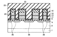
次に、図21に示すように、レジスト膜30を除去した後、コンタクト孔開口の際のエッチングストッパー材となるシリコン窒化膜33を形成する。この後、層間絶縁膜25を形成する。この後、図示はしないがレジスト膜を形成し、このレジスト膜に、ビット線またはソース線コンタクト孔に対応した開口部を開口する。次いで、レジスト膜をマスクに用いて、層間絶縁膜25をエッチング加工し、選択ゲートトランジスタのゲート電極に対して自己整合的にコンタクト孔34を形成する。この後、レジスト膜を除去する。次いで、必要に応じ、コンタクト孔34を介して、p型シリコン基板1(本例ではn型ソース/ドレイン拡散層32)にn型不純物をイオン注入し、n型不純物濃度の濃い領域35を形成する。
【0060】
この後、図18を参照して説明したように、コンタクト孔34内に導電物(コンタクト埋め込み材)を形成し、一般的に知られた方法により配線層を形成し、保護膜を形成して、第2の実施形態に係る不揮発性半導体記憶装置が完成する。
【0061】
(第3の実施形態)
本第3の実施形態は、ビット線またはソース線コンタクト孔が選択ゲートトランジスタのゲート電極間に自己整合的に形成されているNAND型不揮発性半導体記憶装置に関する。そして、このような装置において、コンタクト孔を介して選択ゲートトランジスタのビット線またはソース線コンタクト側にチャネルと同じ導電型の不純物を注入することにより、選択ゲートトランジスタのカットオフ特性を向上させたものである。以下本第3の実施形態に係る装置をその製造方法とともに説明する。
【0062】
まず、第1の実施形態により説明した方法により、図8に示した二層ゲート電極まで形成する。
【0063】
次に、図22に示すように、メモリセルトランジスタ及び選択ゲートトランジスタのゲート電極の側壁を酸化し、酸化膜20を形成する。次いで、図示はしないがレジスト膜を形成し、このレジスト膜に、フォトリソグラフィ法を用いてメモリセル部に対応した開口部を開口する。次いで、レジスト膜をマスクとして、n型不純物、例えばリン(P)を、メモリセルトランジスタ及び選択ゲートトランジスタのソース/ドレイン拡散層領域が形成される領域にイオン注入し、メモリセルトランジスタ及び選択ゲートトランジスタのn型ソース/ドレイン拡散層領域36を形成する。この後、レジスト膜を除去する。
【0064】
次に、図23に示すように、コンタクト孔開口の際のエッチングストッパーとなるシリコン窒化膜33を形成した後、層間絶縁膜25を形成する。
【0065】
次に、図24に示すように、この後、図示はしないがレジスト膜を形成し、このレジスト膜に、ビット線またはソース線コンタクト孔に対応した開口部を開口する。次いで、レジスト膜をマスクに用いて、層間絶縁膜25をエッチング加工し、選択ゲートトランジスタのゲート電極に対して自己整合的にコンタクト孔37を形成する。この後、レジスト膜を除去する。次いで、コンタクト孔37を介して、チャネル(本例ではp型ウェル・チャネル領域3)と同じ導電型のp型不純物、例えばボロン(B)をイオン注入する。なお、このイオン注入は、選択ゲートトランジスタのゲート電極の下に不純物を注入するために、図24中矢印で示すように、角度をつけて2回行うことが望ましい。その結果、選択ゲートトランジスタのゲート電極間のp型シリコン基板1(本例ではp型ウェル・チャネル領域3)内には、p型ウェル・チャネル領域3よりもp型不純物濃度の濃い領域38が形成される。このため、対向する選択ゲートトランジスタ側のn型ソース/ドレイン拡散領域39の実効的な不純物濃度(n型不純物濃度からp型不純物濃度を引いた濃度)は、第1の実施形態と同様に、メモリセルトランジスタ側のn型ソース/ドレイン拡散層領域36の実効的な不純物濃度よりも薄くなる。
【0066】
また、ソース/ドレイン方向におけるpn接合の深さも、対向する選択ゲートトランジスタ側のn型ソース/ドレイン拡散層領域39の方が、メモリセルトランジスタ側のn型ソース/ドレイン拡散層領域36よりも浅くなる。
【0067】
従って、選択ゲートトランジスタのn型ソース/ドレイン拡散層領域36及び39の形状は非対称なものとなり、p型シリコン基板1(本例ではp型ウェル・チャネル領域3)とゲート絶縁膜4との界面からの深さが等しい位置(例えば図24中のB−B’線に沿う位置)で、ビット線またはソース線に接続されるn型ソース/ドレイン拡散層領域39とゲート電極とが重なり合う距離が、メモリセルトランジスタに接続されるn型ソース/ドレイン拡散層領域36とゲート電極とが重なり合う距離よりも小さくなる。
【0068】
このような第3の実施形態に係るNAND型不揮発性半導体記憶装置においても、図24中に示すB−B’線に沿う位置の不純物濃度分布は、第1の実施形態の図15と同様なものになり、第1の実施形態で述べた効果と同様の効果を得ることができる。
【0069】
さらに本第3の実施形態によれば、選択ゲートトランジスタのゲート電極に対して自己整合的に形成されたコンタクト孔を介してイオン注入を行うことにより、第2の実施形態で説明したようなTEOS膜剥離のためのフォトリソグラフィ工程が無い場合でも、チャネルよりも不純物濃度の濃い領域を形成するイオン注入のみを目的としたフォトリソグラフィ工程を増加させることなく、選択ゲートトランジスタのカットオフ特性を向上させることができる。このため、例えば第1の実施形態に比べて、製造コストを下げることができる。
【0070】
ただし、第2の実施形態で説明したようなTEOS膜剥離のためのフォトリソグラフィ工程が有る場合でも、本第3の実施形態のように選択ゲートトランジスタのゲート電極に対して、自己整合的に形成されたコンタクト孔を介してイオン注入を行うことも可能である。この場合にも、製造コストを下げられる利点はある。
【0071】
次いで、必要に応じ、コンタクト孔37を介して、p型シリコン基板1(本例ではn型ソース/ドレイン拡散層39)にn型不純物をイオン注入し、n型不純物濃度の濃い領域40を形成する。
【0072】
この後、図18を参照して説明したように、コンタクト孔37内に導電物(コンタクト埋め込み材)を形成し、一般的に知られた方法により配線層を形成し、保護膜を形成して、第3の実施形態に係る不揮発性半導体記憶装置が完成する。
【0073】
(第4の実施形態)
本第4の実施形態では、メモリセルトランジスタのゲート電極間に不純物が注入されず、選択ゲートトランジスタのゲート電極間のみに不純物が注入されるような角度で、選択ゲートトランジスタのビット線またはソース線コンタクト側にチャネルと同じ導電型の不純物を注入して、選択ゲートトランジスタのカットオフ特性を向上させたものである。
【0074】
まず、第1の実施形態により説明した方法により、図8に示した二層ゲート電極まで形成する。
【0075】
次に、図25に示すように、メモリセルトランジスタ及び選択ゲートトランジスタのゲート電極の側壁を酸化し、酸化膜20を形成する。次いで、図示はしないがレジスト膜を形成し、このレジスト膜に、フォトリソグラフィ法を用いてメモリセル部に対応した開口部を開口する。次いで、チャネル(本例ではp型ウェル・チャネル領域3)と同じ導電型のp型不純物、例えばボロン(B)をイオン注入する。このときのイオン注入の角度θは、以下のようになる。
【0076】
一般に、不揮発性半導体記憶装置において、選択ゲートトランジスタのゲート電極間の距離lSGTは、ビット線またはソース線とコンタクトさせる必要性があることから、メモリセルトランジスタのゲート電極間の距離及びメモリセルトランジスタのゲート電極と選択ゲートトランジスタのゲート電極との間の距離lCE LLよりも大きくなっている。このため、図25に示すように、ゲート電極が遮蔽物となって、メモリセルトランジスタのゲート電極間及びメモリセルトランジスタのゲート電極と選択ゲートトランジスタのゲート電極との間のp型シリコン基板1(本例ではp型ウェル・チャネル領域3)内に、不純物が注入されない角度θ1が存在する。同様に、選択ゲートトランジスタのゲート電極間のp型シリコン基板1内に、不純物が注入されない角度θ2が存在する。従って、イオン注入の角度θを“θ1<θ<θ2”の条件を満たすようにして不純物を注入すると、選択ゲートトランジスタのゲート電極間のp型シリコン基板1内にのみ、不純物を注入することができる。
【0077】
上記角度θ1の具体的規定の一例は、p型シリコン基板1に対して垂直な直線を、選択ゲートトランジスタのゲート電極のメモリセルトランジスタ側側壁最低点を回転中心として回転させたとき、上記直線がメモリセルトランジスタのゲート電極に交わる範囲にある角度である。
【0078】
また、上記角度θ2の具体的規定の一例は、p型シリコン基板1に対して垂直な直線を、選択ゲートトランジスタのゲート電極の対向する選択ゲートトランジスタ側側壁最低点を回転中心として回転させたとき、上記直線が対向する選択ゲートトランジスタのゲート電極に交わらない範囲にある角度である。
【0079】
なお、このイオン注入は、選択ゲートトランジスタのゲート電極の下に不純物を注入するために、図25中矢印で示すように、“±θ”の角度をつけて2回行うことが望ましい。その結果、選択ゲートトランジスタのゲート電極間のp型シリコン基板1内(本例ではp型ウェル・チャネル領域3)には、p型ウェル・チャネル領域3よりもp型不純物濃度の濃い領域41が形成される。
【0080】
次いで、図26に示すように、引き続きメモリセル部に対応した開口部を持つレジスト膜(図示せず)をマスクとして、n型不純物、例えばリン(P)を、メモリセルトランジスタ及び選択ゲートトランジスタのソース/ドレイン拡散層領域が形成される領域にイオン注入し、メモリセルトランジスタ及び選択ゲートトランジスタのn型ソース/ドレイン拡散層領域42、43を形成する。この後、レジスト膜を除去する。
【0081】
このとき、選択ゲートトランジスタのゲート電極間のp型シリコン基板1(本実施形態ではp型ウェル・チャネル領域3)内には、p型ウェル・チャネル領域3よりもp型不純物濃度の濃い領域41が形成されている。このため、対向する選択ゲートトランジスタ側のn型ソース/ドレイン拡散層領域43の実効的な不純物濃度(n型不純物濃度からp型不純物濃度を引いた濃度)は、メモリセルトランジスタ側のn型ソース/ドレイン拡散層42の実効的な不純物濃度よりも薄くなる。
【0082】
また、ソース/ドレイン方向におけるpn接合の深さも、対向する選択ゲートトランジスタ側のn型ソース/ドレイン拡散層領域43の方が、メモリセルトランジスタ側のn型ソース/ドレイン拡散層領域42よりも浅くなる。
【0083】
従って、選択ゲートトランジスタのn型ソース/ドレイン拡散層領域42及び43の形状は非対称なものとなり、p型シリコン基板1(本例ではp型ウェル・チャネル領域3)とゲート絶縁膜4との界面からの深さが等しい位置(例えば図26中のB−B’線に沿う位置)で、ビット線またはソース線に接続されるn型ソース/ドレイン拡散層領域43とゲート電極とが重なり合う距離が、メモリセルトランジスタに接続されるn型ソース/ドレイン拡散層領域42とゲート電極とが重なり合う距離よりも小さくなる。
【0084】
このような第4の実施形態に係るNAND型不揮発性半導体記憶装置においても、図26中に示すB−B’線に沿う位置の不純物濃度分布は、第1の実施形態の図15と同様なものになり、第1の実施形態で述べた効果と同様の効果を得ることができる。
【0085】
さらに本第4の実施形態によれば、イオン注入の角度θを“θ1<θ<θ2”の条件を満たすようにして不純物を注入することにより、チャネルよりも不純物濃度の濃い領域を形成するイオン注入のみを目的としたフォトリソグラフィ工程を増加させることなく、選択ゲートトランジスタのカットオフ特性を向上させることができる。このため、例えば第1の実施形態に比べて、製造コストを下げることができる。
【0086】
次に、図27に示すように、層間絶縁膜25を形成する。この後、図示はしないがレジスト膜を形成し、このレジスト膜に、ビット線またはソース線コンタクト孔に対応した開口部を開口する。次いで、レジスト膜をマスクに用いて、層間絶縁膜25をエッチング加工し、コンタクト孔26を形成する。この後、レジスト膜を除去する。次いで、必要に応じ、コンタクト孔26を介して、p型シリコン基板1(本例ではn型ソース/ドレイン拡散層43)にn型不純物をイオン注入し、n型不純物濃度の濃い領域44を形成する。
【0087】
この後、図18を参照して説明したように、コンタクト孔26内に導電物(コンタクト埋め込み材)を形成し、一般的に知られた方法により配線層を形成し、保護膜を形成して、第2の実施形態に係る不揮発性半導体記憶装置が完成する。
【0088】
なお、本実施形態では、ビット線またはソース線コンタクト孔26を、選択ゲートトランジスタのゲート電極に対して自己整合的に形成していない例を示しているが、ビット線またはソース線コンタクト孔26を、選択ゲートトランジスタのゲート電極に対して自己整合的に形成することも可能である。
【0089】
また、本実施形態では、選択ゲートトランジスタのゲート電極間に、“θ1<θ<θ2”の条件を満たす角度θでp型不純物を、選択ゲートトランジスタのゲート電極間にイオン注入してから、n型ソース/ドレイン拡散層領域42、43を形成するn型不純物をイオン注入しているが、n型ソース/ドレイン拡散層領域42、43を形成するn型不純物をイオン注入してから、選択ゲートトランジスタのゲート電極間に、上記角度θでp型不純物をイオン注入しても良い。
【0090】
以上、この発明を第1〜第4の実施形態により説明したが、この発明は、これら実施形態それぞれに限定されるものではなく、その実施に際しては、発明の要旨を逸脱しない範囲で種々に変形することが可能である。
【0091】
例えば第1〜第4の実施形態では、ウェル・チャネル領域3の形成及びゲート絶縁膜4の形成後に、素子分離領域17の形成を行っているが、素子分離領域17の形成後に、ウェル・チャネル領域3の形成を行ってもかまわない。
【0092】
また、第1〜第4の実施形態では図示していないが、一般的に知られた方法を用いて、一般的に知られた方法を用いてゲート電極に側壁を形成し、n型不純物を濃くイオン注入することにより、メモリセルトランジスタ及び選択ゲートトランジスタのn型ソース/ドレイン拡散層領域をLDD(Lightly Doped Drain)構造にしても良い。
【0093】
また、第1〜第4の実施形態では、複数のメモリセルトランジスタを含むメモリセルユニットを持つ不揮発性半導体記憶装置を例示したが、本発明は、これに限られるものではなく、少なくとも1つのメモリセルトランジスタを含むメモリセルユニットを持つ半導体記憶装置であれば、上記効果をもって適用可能である。
【0094】
また、上記第1〜第4の実施形態はそれぞれ単独、または適宜組み合わせて実施することも、もちろん可能である。
【0095】
さらに上記第1〜第4の実施形態それぞれには、種々の段階の発明が含まれており、上記第1〜第4の実施形態において開示した複数の構成要件の適宜な組み合わせにより、種々の段階の発明を抽出することも可能である。
【0096】
【発明の効果】
以上説明したように、この発明によれば、データ書き込み特性、データ保持特性、読み出しストレスに対する耐性などのメモリセルトランジスタの様々な特性と、選択ゲートトランジスタのカットオフ特性とをともに良好にできる不揮発性半導体記憶装置およびその製造方法を提供できる。
【図面の簡単な説明】
【図1】図1はこの発明の第1の実施形態に係る不揮発性半導体記憶装置の一製造工程を示す断面図。
【図2】図2はこの発明の第1の実施形態に係る不揮発性半導体記憶装置の一製造工程を示す断面図。
【図3】図3はこの発明の第1の実施形態に係る不揮発性半導体記憶装置の一製造工程を示す断面図。
【図4】図4はこの発明の第1の実施形態に係る不揮発性半導体記憶装置の一製造工程を示す断面図。
【図5】図5はこの発明の第1の実施形態に係る不揮発性半導体記憶装置の一製造工程を示す断面図。
【図6】図6はこの発明の第1の実施形態に係る不揮発性半導体記憶装置の一製造工程を示す断面図。
【図7】図7はこの発明の第1の実施形態に係る不揮発性半導体記憶装置のメモリセル部の一部分を示す平面図。
【図8】図8は図7中のA−A’線に沿う断面図。
【図9】図9はこの発明の第1の実施形態に係る不揮発性半導体記憶装置の一製造工程を示す断面図。
【図10】図10はこの発明の第1の実施形態に係る不揮発性半導体記憶装置の一製造工程を示す断面図。
【図11】図11はこの発明の第1の実施形態に係る不揮発性半導体記憶装置の断面図。
【図12】図12は従来の不揮発性半導体記憶装置の断面図。
【図13】図13はこの発明の第1の実施形態に係る不揮発性半導体記憶装置の断面図。
【図14】図14は従来の不揮発性半導体記憶装置の断面図。
【図15】図15はこの発明の第1の実施形態に係る不揮発性半導体記憶装置の不純物濃度分布を示す不純物濃度分布図。
【図16】図16は従来の不揮発性半導体記憶装置の不純物濃度分布を示す不純物濃度分布図。
【図17】図17はこの発明の第1の実施形態に係る不揮発性半導体記憶装置の一製造工程を示す断面図。
【図18】図18はこの発明の第1の実施形態に係る不揮発性半導体記憶装置の一製造工程を示す断面図。
【図19】図19はこの発明の第2の実施形態に係る不揮発性半導体記憶装置の一製造工程を示す断面図。
【図20】図20はこの発明の第2の実施形態に係る不揮発性半導体記憶装置の一製造工程を示す断面図。
【図21】図21はこの発明の第2の実施形態に係る不揮発性半導体記憶装置の一製造工程を示す断面図。
【図22】図22はこの発明の第3の実施形態に係る不揮発性半導体記憶装置の一製造工程を示す断面図。
【図23】図23はこの発明の第3の実施形態に係る不揮発性半導体記憶装置の一製造工程を示す断面図。
【図24】図24はこの発明の第3の実施形態に係る不揮発性半導体記憶装置の一製造工程を示す断面図。
【図25】図25はこの発明の第4の実施形態に係る不揮発性半導体記憶装置の一製造工程を示す断面図。
【図26】図26はこの発明の第4の実施形態に係る不揮発性半導体記憶装置の一製造工程を示す断面図。
【図27】図27はこの発明の第4の実施形態に係る不揮発性半導体記憶装置の一製造工程を示す断面図。
【図28】図28は従来の半導体記憶装置の断面図。
【符号の説明】
1…p型シリコン基板、
2…バッファ酸化膜、
3…p型ウェル・チャネル領域、
4…ゲート絶縁膜、
5…ポリシリコン膜、
6…シリコン窒化膜、
7…レジスト膜、
8…STIの溝、
9…薄いシリコン酸化膜、
10…シリコン酸化膜、
11…ポリシリコン膜、
12…スリット、
13…ONO膜、
14…ポリシリコン/WSi積層膜、
15…シリコン窒化膜、
16…素子領域、
17…素子分離領域、
18…メモリセルトランジスタのゲート電極、
19…選択ゲートトランジスタのゲート電極、
20…酸化膜、
21…レジスト膜、
22…p型不純物濃度の濃い領域、
23…ビット線またはソース線に接するn型ソース/ドレイン拡散層領域、
24…n型ソース/ドレイン拡散層領域、
25…層間絶縁膜、
26…コンタクト孔、
27…n型不純物濃度の濃い領域、
28…n型ソース/ドレイン拡散層領域、
29…TEOS膜などの絶縁膜、
30…レジスト膜、
31…p型不純物濃度の濃い領域、
32…ビット線またはソース線に接するn型ソース/ドレイン拡散層領域、
33…シリコン窒化膜、
34…自己整合的に形成されたコンタクト孔、
35…n型不純物濃度の濃い領域、
36…n型ソース/ドレイン拡散層領域、
37…自己整合的に形成されたコンタクト孔、
38…p型不純物濃度の濃い領域、
39…ビット線またはソース線に接するn型ソース/ドレイン拡散層領域、
40…n型不純物濃度の濃い領域、
41…p型不純物濃度の濃い領域、
42…n型ソース/ドレイン拡散層領域、
43…ビット線またはソース線に接するn型ソース/ドレイン拡散層領域、
44…n型不純物濃度の濃い領域。[0001]
BACKGROUND OF THE INVENTION
The present invention particularly relates to a nonvolatile semiconductor memory device including a memory cell unit including at least one memory cell transistor and a selection gate transistor connected to the memory cell unit, and a method for manufacturing the same.
[0002]
[Prior art]
FIG. 28 is a cross-sectional view of the memory cell transistor and the select gate transistor in the gate length “L” direction in the conventional NAND type semiconductor memory device.
[0003]
A
[0004]
On the other hand, in the selection gate transistor, in order to prevent the TEOS
[0005]
In a NAND type semiconductor memory device, when “1” data is written into a memory cell (electrons are not injected into the floating gate and the threshold value at the time of erasure is maintained), the memory cell transistor is connected via a selection gate transistor. The initial potential is charged from the bit line, the write voltage is applied to the selected word line, the transfer voltage is applied to the non-selected word line, and the potential of the channel region of the memory cell transistor is boosted using capacitive coupling. Electrons are not injected into the
[0006]
[Problems to be solved by the invention]
However, since the impurity distribution in the channel region of the memory cell transistor and the selection gate transistor is the same, by reducing the impurity concentration in the channel region, the threshold voltage of the selection gate transistor decreases, and the off-leakage current increases. There were circumstances that prevented normal operation.
[0007]
The present invention has been made in view of the above circumstances, and its purpose is to provide various characteristics of memory cell transistors such as data write characteristics, data retention characteristics, and resistance to read stress, and cut-off characteristics of select gate transistors. It is an object of the present invention to provide a non-volatile semiconductor memory device and a method of manufacturing the same that can both be improved.
[0008]
[Means for Solving the Problems]
To achieve the above object, a nonvolatile semiconductor memory device according to the first aspect of the present invention is provided.IsA memory cell unit including at least one memory cell transistor having a stacked structure of a charge storage layer and a control gate layer formed on a semiconductor substrate, and one of the source / drain diffusion layer regions is a bit line or a source line And a select gate transistor connected to the memory cell unit on the other side.And beforeThe shape of the source diffusion layer region and the shape of the drain diffusion layer region of the selection gate transistor under the gate electrode of the selection gate transistorIs notSymmetricalThe distance over which the gate electrode overlaps with the diffusion layer region connected to the bit line or the source line at a position where the depth from the interface between the semiconductor substrate and the gate insulating film is equal is connected to the memory cell unit. The effective impurity concentration of the diffusion layer region connected to the bit line or the source line is smaller than the distance over which the diffusion layer region and the gate electrode overlap, and the effective impurity concentration of the diffusion layer region connected to the memory cell unit is The effective impurity concentration of the diffusion layer region that is thinner than the effective impurity concentration and connected to the memory cell unit is the same as the effective impurity concentration of the source / drain diffusion layer region of the memory cell transistor, and the memory On the side of the gate electrode of the cell transistor and the side of the gate electrode of the selection gate transistor that faces the memory cell, A first insulating film, a second insulating film formed on the first insulating film, and a third insulating film formed on the second insulating film, and the selection gate On the side of the gate electrode of the transistor facing the contact for connecting the bit line or the source line, the first insulating film and the third insulating film formed on the first insulating film And are stackedIt is characterized by that.
[0009]
According to such a nonvolatile semiconductor memory device according to the first aspect, the effective gate length of the selection gate transistor is increased by making the shape of the source diffusion layer region and the drain diffusion layer region of the selection gate transistor asymmetric. can do. As a result, the short channel effect of the select gate transistor is improved, and the cut-off characteristic is improved. Further, since the short channel effect of the select gate transistor is improved, the impurity concentration in the channel region of the memory cell transistor can be lowered to a conventional level. As a result, the data write characteristics of the memory cell transistor can be improved.
[0010]
A nonvolatile semiconductor memory device according to the second aspect of the invention is also provided.IsA memory cell unit including at least one memory cell transistor having a stacked structure of a charge storage layer and a control gate layer formed on a semiconductor substrate, and one of the source / drain diffusion layer regions is a bit line or a source line And a select gate transistor connected to the memory cell unit on the other side.The shape of the source diffusion layer region of the selection gate transistor and the shape of the drain diffusion layer region are asymmetric under the gate electrode of the selection gate transistor,At a position where the depth from the interface between the semiconductor substrate and the gate insulating film is equal,The distance between the diffusion layer region connected to the bit line or the source line and the gate electrode is smaller than the distance between the diffusion layer region connected to the memory cell unit and the gate electrode, and the bit line or The impurity concentration of the channel region in contact with the diffusion layer region connected to the source line is higher than the impurity concentration of the channel region in contact with the diffusion layer region connected to the memory cell unit, and the diffusion layer connected to the memory cell unit The impurity concentration of the channel region in contact with the region is the same as the impurity concentration of the channel region in contact with the source / drain diffusion layer region of the memory cell transistor, and the side wall of the gate electrode of the memory cell transistor and the gate of the selection gate transistor On the side of the electrode facing the memory cell, a first insulating film, The second insulating film formed on the first insulating film and the third insulating film formed on the second insulating film are stacked, and the gate electrode of the selection gate transistor, The first insulating film and the third insulating film formed on the first insulating film are stacked on the side facing the contact for connecting the bit line or the source line.It is characterized by that.
[0011]
According to such a non-volatile semiconductor memory device according to the second aspect, the channel region between the source diffusion layer region and the drain diffusion layer region of the selection gate transistor has a region with different impurity concentration, so that the selection is performed. The effective gate length of the gate transistor can be increased. Therefore, the same effect as that of the nonvolatile semiconductor memory device according to the first aspect can be obtained.
[0014]
In addition, the present invention3Method of Manufacturing Nonvolatile Semiconductor Memory Device According to EmbodimentLaw isForming a gate electrode of a memory cell transistor and a select gate transistor having a channel region of a first conductivity type on a semiconductor substrate; and a first insulation on a sidewall of the gate electrode of the memory cell transistor and the select gate transistor Forming a film; forming a second insulating film on the first insulating film; and opening a gate electrode of the selection gate transistor on a side opposite to the side facing the memory cell transistor. A step of forming a mask having a mask, a step of removing the second insulating film through the opening in the mask, and a step through the opening in the mask.Below the gate electrode of the select gate transistorAnd a step of injecting an impurity of the first conductivity type.
[0015]
Like this3According to the method for manufacturing a nonvolatile semiconductor memory device according to the above aspect, a mask for removing the second insulating film from the gate electrode of the select gate transistor is used, and the same as the channel region through the opening of the mask. A conductivity type impurity is implanted. Thus, the nonvolatile semiconductor memory device according to the first and second aspects can be manufactured without increasing the mask formation process for impurity implantation, that is, without increasing the manufacturing cost.
[0018]
In the method for manufacturing a nonvolatile semiconductor memory device according to the fourth aspect of the present invention, a memory cell transistor having a channel region of the first conductivity type and a gate electrode of a selection gate transistor on the semiconductor substrate are used as the selection gate. Forming a space between the gate electrodes of the transistors to be wider than a space between the gate electrode of the memory cell transistor and the gate electrode of the selection gate transistor; and an impurity of a first conductivity type in the semiconductor substrate, Injecting at an angle that is not injected between the gate electrode of the memory cell transistor and the gate electrode of the selection gate transistor but is injected between the gate electrodes of the selection gate transistor.
[0019]
According to the method of manufacturing the nonvolatile semiconductor memory device according to the fourth aspect, an impurity having the same conductivity type as that of the channel region is implanted between the gate electrode of the memory cell transistor and the gate electrode of the selection gate transistor. Instead, the implantation is performed at an angle between the gate electrodes of the selection gate transistors. Thus, the nonvolatile semiconductor memory device according to the first and second aspects can be manufactured without increasing the mask formation process for impurity implantation, that is, without increasing the manufacturing cost.
[0020]
DETAILED DESCRIPTION OF THE INVENTION
Embodiments of the present invention will be described below with reference to the drawings. In the description, common parts are denoted by common reference symbols throughout the drawings.
[0021]
(First embodiment)
The first embodiment improves the cut-off characteristics of the select gate transistor by injecting impurities of the same conductivity type as the channel into the bit line or source line contact side of the select gate transistor connected to the memory cell unit. It is a thing. The NAND nonvolatile semiconductor memory device according to the first embodiment will be described below in detail along with its manufacturing method.
[0022]
First, as shown in FIG. 1, a buffer oxide film 2 is formed on the surface of a p-
[0023]
Next, as shown in FIG. 2, after the buffer oxide film 2 is removed, a
[0024]
Next, as shown in FIG. 3, the silicon nitride film 6 is etched using the resist
[0025]
Next, as shown in FIG. 4, a thin
[0026]
Next, as shown in FIG. 5, polysilicon to be a part of the gate electrode (floating gate) is deposited to form a
[0027]
Next, as shown in FIG. 6, silicon dioxide (O) / silicon nitride (N) / silicon dioxide (O), polysilicon / tungsten silicide (WSi), and silicon nitride are sequentially deposited. In this manner, the
[0028]
Next, although not shown, a resist film is formed, and a pattern corresponding to the gate electrode (control gate and selection gate) is formed on the resist film by photolithography. Next, the
[0029]
7 shows a plan view of a part of the memory cell portion formed by the above method, and FIG. 8 shows a cross section taken along the line A-A 'in FIG.
[0030]
FIG. 7 shows an
[0031]
Next, as shown in FIG. 9, the sidewall of the gate electrode of the memory cell transistor and the sidewall of the gate electrode of the select gate transistor are each oxidized to form an
[0032]
Next, as shown in FIG. 10, after removing the resist
[0033]
At this time, a
[0034]
As shown in FIG. 11, the depth of the pn junction in the source / drain direction is the depth of the pn junction D1 of the n-type source / drain
[0035]
When p-type impurities are not ion-implanted between the gate electrodes of the selection gate transistor, which is a conventional example, the depth is reduced below the
[0036]
Further, as shown in FIG. 13, the shape of the n-type source / drain
[0037]
In the case where p-type impurities are not ion-implanted between the gate electrodes of the selection gate transistor, which is a conventional example, the distance L1 is the same as L2 as shown in FIG.
[0038]
FIG. 15 shows an impurity concentration distribution at a position along the line B-B ′ in FIG. 10 (or FIG. 13).
[0039]
As shown in FIG. 15, in the select gate transistor, the impurity concentration of the channel region differs in the direction from the n-type source /
[0040]
The impurity concentration of the channel region in contact with the n-type source / drain
[0041]
FIG. 16 shows an impurity concentration distribution when p-type impurities are not ion-implanted between the gate electrodes of the select gate transistor, which is a conventional example. FIG. 16 shows an impurity concentration distribution at a position along the line B-B ′ in FIG. 28. The position of the B-B ′ line in FIG. 28 is the same as the position of the B-B ′ line shown in FIG. 15.
[0042]
Compared with the conventional example shown in FIG. 16, in the present embodiment shown in FIG. 15, the effective channel length of the select gate transistor is increased.
[0043]
Thus, in this embodiment, the effective channel length of the select gate transistor is increased by ion-implanting the same p-type impurity as that of the channel between the gate electrodes of the select gate transistor. Thereby, the short channel effect of the select gate transistor is improved, and the cut-off characteristic is improved.
[0044]
Further, since the cut-off characteristics of the select gate transistor are improved, the impurity concentration in the channel region of the memory cell transistor can be lowered below the conventional level. As a result, the “1” data write characteristic is improved in the memory cell transistor. That is, for example, in a NAND type nonvolatile semiconductor memory device having a memory cell unit including a plurality of memory cell transistors as in the present embodiment, the resistance to non-selective write stress is further improved.
[0045]
In this embodiment, the threshold voltage of the selection gate transistor and the threshold voltage of the memory cell transistor are set within a range in which the threshold voltage of the selection gate transistor is higher than the threshold voltage of the memory cell transistor. Can be controlled independently. Therefore, it is possible to improve various characteristics of the memory cell transistor such as data retention characteristics and resistance to read stress while maintaining the cut-off characteristics of the selection gate transistor.
[0046]
In other words, the effect of the present embodiment is not particularly limited to the NAND type nonvolatile semiconductor memory device, and if it is a nonvolatile semiconductor memory device having a structure in which the select gate transistor is connected to the memory cell transistor, It is obtained effectively.
[0047]
Next, as shown in FIG. 17, an
[0048]
Next, as shown in FIG. 18, a conductor (contact filling material: plug) is formed in the
[0049]
In this embodiment, the p-type impurity is ion-implanted between the gate electrodes of the selection gate transistor, and then the n-type impurity forming the n-type source / drain
[0050]
(Second Embodiment)
In the second embodiment, an insulating film such as a TEOS film is formed on the side walls of the gate electrodes of the memory cell transistor and the select gate transistor, and the bit line or source line contact hole is self-aligned between the gate electrodes of the select gate transistor. The present invention relates to a NAND type nonvolatile semiconductor memory device having a structure in which a TEOS film between a gate electrode of a select gate transistor and a contact hole is peeled off. In such a device, an impurity having the same conductivity type as that of the channel is implanted into the bit line or source line contact hole side of the select gate transistor, thereby improving the cut-off characteristics of the select gate transistor. The apparatus according to the second embodiment will be described below together with its manufacturing method.
[0051]
First, the double-layer gate electrode shown in FIG. 8 is formed by the method described in the first embodiment.
[0052]
Next, as shown in FIG. 19, the side walls of the gate electrodes of the memory cell transistor and the select gate transistor are oxidized to form an
[0053]
Next, as shown in FIG. 20, a resist
[0054]
The depth of the pn junction in the source / drain direction is also shallower in the n-type source / drain
[0055]
Therefore, the shape of the n-type source / drain
[0056]
Also in the NAND-type nonvolatile semiconductor memory device according to the second embodiment, the impurity concentration distribution at the position along the line BB ′ shown in FIG. 20 is the same as that in FIG. 15 of the first embodiment. Thus, the same effects as described in the first embodiment can be obtained.
[0057]
Further, according to the second embodiment, ion implantation is performed using the resist
[0058]
Note that the ion implantation described with reference to FIG. 20 is performed after the
[0059]
Next, as shown in FIG. 21, after removing the resist
[0060]
Thereafter, as described with reference to FIG. 18, a conductive material (contact filling material) is formed in the
[0061]
(Third embodiment)
The third embodiment relates to a NAND-type nonvolatile semiconductor memory device in which bit line or source line contact holes are formed in a self-aligned manner between gate electrodes of select gate transistors. In such a device, an impurity having the same conductivity type as that of the channel is injected into the bit line or source line contact side of the selection gate transistor through the contact hole, thereby improving the cutoff characteristic of the selection gate transistor. It is. The apparatus according to the third embodiment will be described below together with its manufacturing method.
[0062]
First, the double-layer gate electrode shown in FIG. 8 is formed by the method described in the first embodiment.
[0063]
Next, as shown in FIG. 22, the side walls of the gate electrodes of the memory cell transistor and the select gate transistor are oxidized to form an
[0064]
Next, as shown in FIG. 23, after forming a
[0065]
Next, as shown in FIG. 24, although not shown, a resist film is formed, and openings corresponding to the bit line or source line contact holes are opened in the resist film. Next, using the resist film as a mask, the
[0066]
In addition, the depth of the pn junction in the source / drain direction is also shallower in the n-type source / drain
[0067]
Therefore, the shape of the n-type source / drain
[0068]
Also in the NAND-type nonvolatile semiconductor memory device according to the third embodiment, the impurity concentration distribution at the position along the line BB ′ shown in FIG. 24 is the same as that in FIG. 15 of the first embodiment. Thus, the same effects as described in the first embodiment can be obtained.
[0069]
Furthermore, according to the third embodiment, TEOS as described in the second embodiment is performed by performing ion implantation through a contact hole formed in a self-aligned manner with respect to the gate electrode of the select gate transistor. Even when there is no photolithography process for film separation, the cutoff characteristics of the select gate transistor are improved without increasing the photolithography process only for ion implantation for forming a region having a higher impurity concentration than the channel. be able to. For this reason, for example, compared with 1st Embodiment, a manufacturing cost can be lowered | hung.
[0070]
However, even when there is a photolithography process for peeling the TEOS film as described in the second embodiment, it is formed in a self-aligned manner with respect to the gate electrode of the select gate transistor as in the third embodiment. It is also possible to perform ion implantation through the formed contact hole. Also in this case, there is an advantage that the manufacturing cost can be reduced.
[0071]
Next, if necessary, n-type impurities are ion-implanted into the p-type silicon substrate 1 (in this example, the n-type source / drain diffusion layer 39) through the contact holes 37 to form a
[0072]
Thereafter, as described with reference to FIG. 18, a conductive material (contact filling material) is formed in the
[0073]
(Fourth embodiment)
In the fourth embodiment, the bit line or the source line of the selection gate transistor is at an angle such that the impurity is not injected between the gate electrodes of the memory cell transistor and the impurity is injected only between the gate electrodes of the selection gate transistor. An impurity having the same conductivity type as that of the channel is implanted on the contact side to improve the cut-off characteristics of the select gate transistor.
[0074]
First, the double-layer gate electrode shown in FIG. 8 is formed by the method described in the first embodiment.
[0075]
Next, as shown in FIG. 25, the side walls of the gate electrodes of the memory cell transistor and the select gate transistor are oxidized to form an
[0076]
Generally, in a nonvolatile semiconductor memory device, a distance l between gate electrodes of select gate transistorsSGTSince it is necessary to make contact with the bit line or the source line, the distance between the gate electrodes of the memory cell transistor and the distance l between the gate electrode of the memory cell transistor and the gate electrode of the selection gate transistorCE LLIs bigger than. For this reason, as shown in FIG. 25, the gate electrode serves as a shield, and the p-type silicon substrate 1 (between the gate electrodes of the memory cell transistor and between the gate electrode of the memory cell transistor and the gate electrode of the selection gate transistor) In this example, an angle θ1 at which impurities are not implanted exists in the p-type well channel region 3). Similarly, there is an angle θ2 at which impurities are not implanted in the p-
[0077]
An example of the specific definition of the angle θ1 is that when a straight line perpendicular to the p-
[0078]
An example of the specific definition of the angle θ2 is that a straight line perpendicular to the p-
[0079]
Note that this ion implantation is desirably performed twice at an angle of “± θ” as indicated by an arrow in FIG. 25 in order to implant an impurity under the gate electrode of the selection gate transistor. As a result, a
[0080]
Next, as shown in FIG. 26, using a resist film (not shown) having an opening corresponding to the memory cell portion as a mask, an n-type impurity such as phosphorus (P) is applied to the memory cell transistor and the select gate transistor. Ions are implanted into the region where the source / drain diffusion layer region is formed, thereby forming n-type source / drain
[0081]
At this time, a
[0082]
The depth of the pn junction in the source / drain direction is also shallower in the n-type source / drain
[0083]
Therefore, the shape of the n-type source / drain
[0084]
Also in the NAND-type nonvolatile semiconductor memory device according to the fourth embodiment, the impurity concentration distribution at the position along the line BB ′ shown in FIG. 26 is the same as that in FIG. 15 of the first embodiment. Thus, the same effects as described in the first embodiment can be obtained.
[0085]
Furthermore, according to the fourth embodiment, by implanting impurities so that the angle of ion implantation θ satisfies the condition of “θ1 <θ <θ2”, ions forming a region having a higher impurity concentration than the channel are formed. The cut-off characteristics of the select gate transistor can be improved without increasing the photolithography process for the purpose of implantation only. For this reason, for example, compared with 1st Embodiment, a manufacturing cost can be lowered | hung.
[0086]
Next, as shown in FIG. 27, an
[0087]
Thereafter, as described with reference to FIG. 18, a conductive material (contact filling material) is formed in the
[0088]
In this embodiment, an example in which the bit line or source
[0089]
In this embodiment, a p-type impurity is ion-implanted between the gate electrodes of the selection gate transistors at an angle θ that satisfies the condition of “θ1 <θ <θ2”, and then n The n-type impurity forming the source / drain
[0090]
As mentioned above, although this invention was demonstrated by 1st-4th embodiment, this invention is not limited to each of these embodiment, In the case of implementation, it changes variously in the range which does not deviate from the summary of invention. Is possible.
[0091]
For example, in the first to fourth embodiments, the
[0092]
Although not shown in the first to fourth embodiments, a side wall is formed on the gate electrode using a generally known method, and an n-type impurity is introduced. The n-type source / drain diffusion layer regions of the memory cell transistor and the select gate transistor may have an LDD (Lightly Doped Drain) structure by deep ion implantation.
[0093]
In the first to fourth embodiments, the nonvolatile semiconductor memory device having a memory cell unit including a plurality of memory cell transistors is exemplified. However, the present invention is not limited to this, and at least one memory is used. Any semiconductor memory device having a memory cell unit including a cell transistor can be applied with the above effects.
[0094]
Of course, the first to fourth embodiments can be implemented individually or in appropriate combination.
[0095]
Further, each of the first to fourth embodiments includes inventions of various stages, and various stages can be achieved by appropriately combining a plurality of constituent elements disclosed in the first to fourth embodiments. It is also possible to extract the invention.
[0096]
【The invention's effect】
As described above, according to the present invention, the non-volatile property that can improve both the various characteristics of the memory cell transistor such as the data write characteristic, the data retention characteristic, and the resistance to the read stress, and the cut-off characteristic of the selection gate transistor. A semiconductor memory device and a manufacturing method thereof can be provided.
[Brief description of the drawings]
FIG. 1 is a cross-sectional view showing one manufacturing process of a nonvolatile semiconductor memory device according to a first embodiment of the present invention;
FIG. 2 is a cross-sectional view showing one manufacturing process of the nonvolatile semiconductor memory device according to the first embodiment of the invention.
FIG. 3 is a cross-sectional view showing one manufacturing process of the nonvolatile semiconductor memory device in accordance with the first embodiment of the present invention.
FIG. 4 is a cross-sectional view showing one manufacturing process of the nonvolatile semiconductor memory device according to the first embodiment of the present invention.
FIG. 5 is a cross-sectional view showing one manufacturing process of the nonvolatile semiconductor memory device in accordance with the first embodiment of the present invention.
FIG. 6 is a cross-sectional view showing one manufacturing process of the nonvolatile semiconductor memory device in accordance with the first embodiment of the present invention.
FIG. 7 is a plan view showing a part of the memory cell portion of the nonvolatile semiconductor memory device according to the first embodiment of the invention.
8 is a cross-sectional view taken along line A-A ′ in FIG. 7;
FIG. 9 is a cross-sectional view showing one manufacturing process of the nonvolatile semiconductor memory device in accordance with the first embodiment of the present invention.
FIG. 10 is a cross-sectional view showing one manufacturing process of the nonvolatile semiconductor memory device in accordance with the first embodiment of the present invention.
FIG. 11 is a sectional view of the nonvolatile semiconductor memory device according to the first embodiment of the invention.
FIG. 12 is a cross-sectional view of a conventional nonvolatile semiconductor memory device.
FIG. 13 is a cross-sectional view of the nonvolatile semiconductor memory device according to the first embodiment of the invention.
FIG. 14 is a cross-sectional view of a conventional nonvolatile semiconductor memory device.
FIG. 15 is an impurity concentration distribution diagram showing an impurity concentration distribution of the nonvolatile semiconductor memory device according to the first embodiment of the present invention.
FIG. 16 is an impurity concentration distribution diagram showing an impurity concentration distribution of a conventional nonvolatile semiconductor memory device.
FIG. 17 is a cross-sectional view showing one manufacturing process of the nonvolatile semiconductor memory device in accordance with the first embodiment of the present invention.
FIG. 18 is a cross-sectional view showing one manufacturing process of the nonvolatile semiconductor memory device in accordance with the first embodiment of the present invention.
FIG. 19 is a cross-sectional view showing one manufacturing process of the nonvolatile semiconductor memory device in accordance with the second embodiment of the present invention.
FIG. 20 is a cross-sectional view showing one manufacturing process of the nonvolatile semiconductor memory device in accordance with the second embodiment of the present invention.
FIG. 21 is a cross-sectional view showing one manufacturing process of the nonvolatile semiconductor memory device according to the second embodiment of the present invention;
FIG. 22 is a cross-sectional view showing one manufacturing process of the nonvolatile semiconductor memory device in accordance with the third embodiment of the present invention.
FIG. 23 is a cross-sectional view showing a manufacturing process of the nonvolatile semiconductor memory device in accordance with the third embodiment of the present invention.
FIG. 24 is a cross-sectional view showing one manufacturing process of the nonvolatile semiconductor memory device in accordance with the third embodiment of the present invention.
FIG. 25 is a sectional view showing one manufacturing process of the nonvolatile semiconductor memory device according to the fourth embodiment of the present invention;
FIG. 26 is a cross-sectional view showing one manufacturing process of the nonvolatile semiconductor memory device in accordance with the fourth embodiment of the present invention.
FIG. 27 is a sectional view showing one manufacturing process of the nonvolatile semiconductor memory device according to the fourth embodiment of the present invention;
FIG. 28 is a cross-sectional view of a conventional semiconductor memory device.
[Explanation of symbols]
1 ... p-type silicon substrate,
2. Buffer oxide film,
3 ... p-type well channel region,
4 ... Gate insulating film,
5 ... polysilicon film,
6 ... silicon nitride film,
7 ... resist film,
8 ... STI groove,
9: Thin silicon oxide film,
10: Silicon oxide film,
11 ... polysilicon film,
12 ... Slit,
13 ... ONO film,
14 ... Polysilicon / WSi laminated film,
15 ... Silicon nitride film,
16: Element region,
17 ... element isolation region,
18 ... Gate electrode of memory cell transistor,
19 ... gate electrode of select gate transistor,
20 ... Oxide film,
21 ... resist film,
22 ... a region having a high p-type impurity concentration,
23, n-type source / drain diffusion layer region in contact with the bit line or the source line,
24 ... n-type source / drain diffusion layer region,
25. Interlayer insulating film,
26 ... contact hole,
27: a region having a high n-type impurity concentration,
28 ... n-type source / drain diffusion layer region,
29. Insulating film such as TEOS film,
30 ... resist film,
31 ... a region having a high p-type impurity concentration,
32... N-type source / drain diffusion layer region in contact with the bit line or the source line,
33 ... Silicon nitride film,
34 ... Contact hole formed in a self-aligning manner,
35 ... a region having a high n-type impurity concentration,
36 ... n-type source / drain diffusion layer region,
37 ... Contact hole formed in a self-aligning manner,
38 ... a region having a high p-type impurity concentration,
39... N-type source / drain diffusion layer region in contact with the bit line or the source line,
40 ... a region having a high n-type impurity concentration,
41 ... a region having a high p-type impurity concentration,
42 ... n-type source / drain diffusion layer region,
43. n-type source / drain diffusion layer region in contact with the bit line or the source line,
44: A region having a high n-type impurity concentration.
Claims (9)
ソース/ドレイン拡散層領域の一方がビット線またはソース線に接続され、他方が前記メモリセルユニットに接続された選択ゲートトランジスタとを具備し、
前記選択ゲートトランジスタのゲート電極下で、この選択ゲートトランジスタのソース拡散層領域の形状とドレイン拡散層領域の形状とが非対称であり、
前記半導体基板とゲート絶縁膜との界面からの深さが等しい位置で、前記ビット線またはソース線に接続された拡散層領域と前記ゲート電極とが重なり合う距離が、前記メモリセルユニットに接続された拡散層領域と前記ゲート電極とが重なり合う距離よりも小さく、前記ビット線またはソース線に接続された拡散層領域の実効的な不純物濃度が、前記メモリセルユニットに接続された拡散層領域の実効不純物濃度よりも薄く、前記メモリセルユニットに接続された拡散層領域の実効的な不純物濃度が、前記メモリセルトランジスタのソース/ドレイン拡散層領域の実効的な不純物濃度と同じであり、前記メモリセルトランジスタのゲート電極の側壁、及び前記選択ゲートトランジスタのゲート電極の前記メモリセルに対向する側には、第1の絶縁膜と、この第1の絶縁膜上に形成された第2の絶縁膜と、この第2の絶縁膜上に形成された第3の絶縁膜とが積層されており、前記選択ゲートトランジスタのゲート電極の、前記ビット線またはソース線を接続するためのコンタクトに対向する側には、前記第1の絶縁膜と、この第1の絶縁膜上に形成された前記第3の絶縁膜とが積層されていることを特徴とする不揮発性半導体記憶装置。A memory cell unit including at least one memory cell transistor having a stacked structure of a charge storage layer and a control gate layer formed on a semiconductor substrate;
A selection gate transistor in which one of the source / drain diffusion layer regions is connected to the bit line or the source line and the other is connected to the memory cell unit;
Under the gate electrode of the selection gate transistor, the shape of the source diffusion layer region of the selection gate transistor and the shape of the drain diffusion layer region are asymmetric.
The distance between the diffusion layer region connected to the bit line or the source line and the gate electrode at a position where the depth from the interface between the semiconductor substrate and the gate insulating film is equal is connected to the memory cell unit. diffusion layer region and the rather smaller than the distance where the gate electrode overlaps, the effective impurity concentration of the connected diffusion layer region to the bit line or the source line, effective of the connected to the memory cell unit diffusion layer region The effective impurity concentration of the diffusion layer region that is thinner than the impurity concentration and connected to the memory cell unit is the same as the effective impurity concentration of the source / drain diffusion layer region of the memory cell transistor, and the memory cell A side wall of the gate electrode of the transistor and a side of the gate electrode of the select gate transistor facing the memory cell An insulating film, a second insulating film formed on the first insulating film, and a third insulating film formed on the second insulating film are stacked, and the select gate transistor On the side of the gate electrode facing the contact for connecting the bit line or the source line, the first insulating film and the third insulating film formed on the first insulating film are provided. A non-volatile semiconductor memory device, characterized by being stacked .
ソース/ドレイン拡散層領域の一方がビット線またはソース線に接続され、他方が前記メモリセルユニットに接続された選択ゲートトランジスタとを具備し、
前記選択ゲートトランジスタのゲート電極下で、この選択ゲートトランジスタのソース拡散層領域の形状とドレイン拡散層領域の形状とが非対称であり、
前記半導体基板とゲート絶縁膜との界面からの深さが等しい位置で、前記ビット線またはソース線に接続された拡散層領域と前記ゲート電極とが重なり合う距離が、前記メモリセルユニットに接続された拡散層領域と前記ゲート電極とが重なり合う距離よりも小さく、前記ビット線またはソース線に接続された拡散層領域に接するチャネル領域の不純物濃度が、前記メモリセルユニットに接続された拡散層領域に接するチャネル領域の不純物濃度よりも濃く、前記メモリセルユニットに接続された拡散層領域に接するチャネル領域の不純物濃度が、前記メモリセルトランジスタのソース/ドレイン拡散層領域に接するチャネル領域の不純物濃度と同じであり、前記メモリセルトランジスタのゲート電極の側壁、及び前記選択ゲートトランジスタのゲート電極の前記メモリセルに対向する側には、第1の絶縁膜と、この第1の絶縁膜上に形成された第2の絶縁膜と、この第2の絶縁膜上に形成された第3の絶縁膜とが積層されており、前記選択ゲートトランジスタのゲート電極の、前記ビット線またはソース線を接続するためのコンタクトに対向する側には、前記第1の絶縁膜と、この第1の絶縁膜上に形成された前記第3の絶縁膜とが積層されていることを特徴とする不揮発性半導体記憶装置。A memory cell unit including at least one memory cell transistor having a stacked structure of a charge storage layer and a control gate layer formed on a semiconductor substrate;
A selection gate transistor in which one of the source / drain diffusion layer regions is connected to the bit line or the source line and the other is connected to the memory cell unit;
Under the gate electrode of the selection gate transistor, the shape of the source diffusion layer region of the selection gate transistor and the shape of the drain diffusion layer region are asymmetric.
The distance between the diffusion layer region connected to the bit line or the source line and the gate electrode at a position where the depth from the interface between the semiconductor substrate and the gate insulating film is equal is connected to the memory cell unit. The impurity concentration of the channel region that is smaller than the distance between the diffusion layer region and the gate electrode and that is in contact with the diffusion layer region connected to the bit line or source line is in contact with the diffusion layer region connected to the memory cell unit. The impurity concentration of the channel region that is higher than the impurity concentration of the channel region and is in contact with the diffusion layer region connected to the memory cell unit is the same as the impurity concentration of the channel region that is in contact with the source / drain diffusion layer region of the memory cell transistor. A sidewall of the gate electrode of the memory cell transistor, and the selection gate transistor On the side of the gate electrode facing the memory cell, a first insulating film, a second insulating film formed on the first insulating film, and a second insulating film are formed on the second insulating film. A third insulating film is stacked, and on the side of the gate electrode of the select gate transistor facing the contact for connecting the bit line or the source line, the first insulating film and the first insulating film are formed. A non-volatile semiconductor memory device , wherein the third insulating film formed on one insulating film is laminated .
前記メモリセルトランジスタ及び前記選択ゲートトランジスタのゲート電極の側壁に第1の絶縁膜を形成する工程と、
前記第1の絶縁膜上に、第2の絶縁膜を形成する工程と、
前記選択ゲートトランジスタのゲート電極の、前記メモリセルトランジスタに対向する側とは反対側に開口を持つマスクを形成する工程と、
前記マスクの開口を介して前記第2の絶縁膜を除去する工程と、
前記マスクの開口を介して前記選択ゲートトランジスタのゲート電極下に第1導電型の不純物を注入する工程と
を具備することを特徴とする不揮発性半導体記憶装置の製造方法。 Forming a gate electrode of a memory cell transistor having a first conductivity type channel region and a selection gate transistor on a semiconductor substrate;
Forming a first insulating film on a sidewall of the gate electrode of the memory cell transistor and the selection gate transistor;
Forming a second insulating film on the first insulating film;
Forming a mask having an opening on a side of the gate electrode of the selection gate transistor opposite to the side facing the memory cell transistor;
Removing the second insulating film through the opening of the mask;
Implanting a first conductivity type impurity under the gate electrode of the select gate transistor through the opening of the mask;
Method of manufacturing a nonvolatile semiconductor memory device you characterized by comprising a.
前記半導体基板に第1導電型の不純物を、前記メモリセルトランジスタのゲート電極と選択ゲートトランジスタのゲート電極との間には注入されず、前記選択ゲートトランジスタのゲート電極間に注入される角度で注入する工程と
を具備することを特徴とする不揮発性半導体記憶装置の製造方法。 A gate electrode of a memory cell transistor and a select gate transistor having a channel region of the first conductivity type on a semiconductor substrate, a space between the gate electrodes of the select gate transistor, a gate electrode of the transistor of the memory cell and the select gate Forming wider than the space between the gate electrodes of the transistor;
The first conductivity type impurity is not injected between the gate electrode of the memory cell transistor and the gate electrode of the selection gate transistor, but at an angle that is injected between the gate electrodes of the selection gate transistor. And the process
Method of manufacturing a nonvolatile semiconductor memory device you characterized by comprising a.
Priority Applications (7)
| Application Number | Priority Date | Filing Date | Title |
|---|---|---|---|
| JP2001023973A JP4309070B2 (en) | 2001-01-31 | 2001-01-31 | Nonvolatile semiconductor memory device and manufacturing method thereof |
| US10/058,343 US6835987B2 (en) | 2001-01-31 | 2002-01-30 | Non-volatile semiconductor memory device in which selection gate transistors and memory cells have different structures |
| US10/942,013 US6949794B2 (en) | 2001-01-31 | 2004-09-16 | Non-volatile semiconductor memory device in which selection gate transistors and memory cells have different structures |
| US11/225,094 US7122869B2 (en) | 2001-01-31 | 2005-09-14 | Nonvolatile semiconductor memory device in which selection transistors and memory transistors have different impurity concentration distributions |
| US11/538,944 US7274075B2 (en) | 2001-01-31 | 2006-10-05 | Nonvolatile semiconductor memory device having pair of selection transistors with different source and drain impurity concentrations and with different channel dopant concentrations |
| US11/857,934 US7737508B2 (en) | 2001-01-31 | 2007-09-19 | Non-volatile semiconductor memory device and method of manufacturing the same |
| US12/779,357 US8338252B2 (en) | 2001-01-31 | 2010-05-13 | Non-volatile semiconductor memory device and method of manufacturing the same |
Applications Claiming Priority (1)
| Application Number | Priority Date | Filing Date | Title |
|---|---|---|---|
| JP2001023973A JP4309070B2 (en) | 2001-01-31 | 2001-01-31 | Nonvolatile semiconductor memory device and manufacturing method thereof |
Publications (3)
| Publication Number | Publication Date |
|---|---|
| JP2002231832A JP2002231832A (en) | 2002-08-16 |
| JP2002231832A5 JP2002231832A5 (en) | 2005-10-06 |
| JP4309070B2 true JP4309070B2 (en) | 2009-08-05 |
Family
ID=18889180
Family Applications (1)
| Application Number | Title | Priority Date | Filing Date |
|---|---|---|---|
| JP2001023973A Expired - Fee Related JP4309070B2 (en) | 2001-01-31 | 2001-01-31 | Nonvolatile semiconductor memory device and manufacturing method thereof |
Country Status (1)
| Country | Link |
|---|---|
| JP (1) | JP4309070B2 (en) |
Families Citing this family (7)
| Publication number | Priority date | Publication date | Assignee | Title |
|---|---|---|---|---|
| KR100524993B1 (en) | 2003-11-28 | 2005-10-31 | 삼성전자주식회사 | EEPROM cell and EEPROM device having high integration and low source resistance and method for fabricating the same |
| JP2005327792A (en) * | 2004-05-12 | 2005-11-24 | Toshiba Corp | Semiconductor device and its manufacturing method |
| JP2009081202A (en) | 2007-09-25 | 2009-04-16 | Toshiba Corp | Semiconductor memory device and its manufacturing method |
| KR100884344B1 (en) | 2007-10-10 | 2009-02-18 | 주식회사 하이닉스반도체 | Non-volatile memory device having asymmetric source/drain junction and method for fabricating the same |
| JP2010161301A (en) | 2009-01-09 | 2010-07-22 | Toshiba Corp | Semiconductor memory device and method of manufacturing the same |
| JP2012059945A (en) | 2010-09-09 | 2012-03-22 | Toshiba Corp | Semiconductor device and method for manufacturing the same |
| JP2013187504A (en) * | 2012-03-09 | 2013-09-19 | Toshiba Corp | Nonvolatile semiconductor storage device and manufacturing method of the same |
-
2001
- 2001-01-31 JP JP2001023973A patent/JP4309070B2/en not_active Expired - Fee Related
Also Published As
| Publication number | Publication date |
|---|---|
| JP2002231832A (en) | 2002-08-16 |
Similar Documents
| Publication | Publication Date | Title |
|---|---|---|
| US6835987B2 (en) | Non-volatile semiconductor memory device in which selection gate transistors and memory cells have different structures | |
| US10741570B2 (en) | Nonvolatile memory devices having single-layered gates and methods of fabricating the same | |
| US6716703B2 (en) | Method of making semiconductor memory device having sources connected to source lines | |
| US6376879B2 (en) | Semiconductor device having MISFETs | |
| KR100398955B1 (en) | Eeprom memory cell and method of forming the same | |
| US20030013253A1 (en) | Optimized flash memory cell | |
| JP2004241780A (en) | Method of manufacturing semiconductor integrated circuit using selective disposable spacer technology, and semiconductor integrated circuit manufactured thereby | |
| KR20020011317A (en) | Semiconductor memory device and manufacturing method thereof | |
| US8952536B2 (en) | Semiconductor device and method of fabrication | |
| JP4445353B2 (en) | Manufacturing method of direct tunnel semiconductor memory device | |
| US20080023748A1 (en) | Self-aligned contacts to source/drain regions | |
| US20030011023A1 (en) | Metal local interconnect self-aligned source flash cell | |
| JP4217409B2 (en) | Nonvolatile memory device and manufacturing method thereof | |
| JP4972918B2 (en) | Semiconductor device and manufacturing method thereof | |
| JP4309070B2 (en) | Nonvolatile semiconductor memory device and manufacturing method thereof | |
| KR20070049731A (en) | Flash memory and manufacturing method thereof | |
| JPWO2003069675A1 (en) | Manufacturing method of semiconductor device | |
| US8878253B2 (en) | Semiconductor devices | |
| JP2002289706A (en) | Nonvolatile semiconductor memory device and its manufacturing method | |
| JP3669070B2 (en) | Semiconductor device and manufacturing method thereof | |
| JP4031777B2 (en) | Semiconductor device | |
| KR20080100968A (en) | Non-volatile memory device and manufacturing method thereof | |
| KR20100126952A (en) | Nonvolatile memory device and manufacturing method of the same |
Legal Events
| Date | Code | Title | Description |
|---|---|---|---|
| A521 | Request for written amendment filed |
Free format text: JAPANESE INTERMEDIATE CODE: A523 Effective date: 20050518 |
|
| A621 | Written request for application examination |
Free format text: JAPANESE INTERMEDIATE CODE: A621 Effective date: 20050518 |
|
| A977 | Report on retrieval |
Free format text: JAPANESE INTERMEDIATE CODE: A971007 Effective date: 20071015 |
|
| A131 | Notification of reasons for refusal |
Free format text: JAPANESE INTERMEDIATE CODE: A131 Effective date: 20080722 |
|
| A521 | Request for written amendment filed |
Free format text: JAPANESE INTERMEDIATE CODE: A523 Effective date: 20080917 |
|
| TRDD | Decision of grant or rejection written | ||
| A01 | Written decision to grant a patent or to grant a registration (utility model) |
Free format text: JAPANESE INTERMEDIATE CODE: A01 Effective date: 20090407 |
|
| A01 | Written decision to grant a patent or to grant a registration (utility model) |
Free format text: JAPANESE INTERMEDIATE CODE: A01 |
|
| A61 | First payment of annual fees (during grant procedure) |
Free format text: JAPANESE INTERMEDIATE CODE: A61 Effective date: 20090507 |
|
| FPAY | Renewal fee payment (event date is renewal date of database) |
Free format text: PAYMENT UNTIL: 20120515 Year of fee payment: 3 |
|
| FPAY | Renewal fee payment (event date is renewal date of database) |
Free format text: PAYMENT UNTIL: 20120515 Year of fee payment: 3 |
|
| FPAY | Renewal fee payment (event date is renewal date of database) |
Free format text: PAYMENT UNTIL: 20130515 Year of fee payment: 4 |
|
| FPAY | Renewal fee payment (event date is renewal date of database) |
Free format text: PAYMENT UNTIL: 20130515 Year of fee payment: 4 |
|
| FPAY | Renewal fee payment (event date is renewal date of database) |
Free format text: PAYMENT UNTIL: 20140515 Year of fee payment: 5 |
|
| LAPS | Cancellation because of no payment of annual fees |