JP4293302B2 - Method and apparatus for maintaining a constant load current with line voltage in a switch mode power supply - Google Patents
Method and apparatus for maintaining a constant load current with line voltage in a switch mode power supply Download PDFInfo
- Publication number
- JP4293302B2 JP4293302B2 JP2002284064A JP2002284064A JP4293302B2 JP 4293302 B2 JP4293302 B2 JP 4293302B2 JP 2002284064 A JP2002284064 A JP 2002284064A JP 2002284064 A JP2002284064 A JP 2002284064A JP 4293302 B2 JP4293302 B2 JP 4293302B2
- Authority
- JP
- Japan
- Prior art keywords
- current
- output
- power supply
- limit threshold
- switching device
- Prior art date
- Legal status (The legal status is an assumption and is not a legal conclusion. Google has not performed a legal analysis and makes no representation as to the accuracy of the status listed.)
- Expired - Fee Related
Links
Images


Classifications
-
- H—ELECTRICITY
- H02—GENERATION; CONVERSION OR DISTRIBUTION OF ELECTRIC POWER
- H02M—APPARATUS FOR CONVERSION BETWEEN AC AND AC, BETWEEN AC AND DC, OR BETWEEN DC AND DC, AND FOR USE WITH MAINS OR SIMILAR POWER SUPPLY SYSTEMS; CONVERSION OF DC OR AC INPUT POWER INTO SURGE OUTPUT POWER; CONTROL OR REGULATION THEREOF
- H02M3/00—Conversion of dc power input into dc power output
- H02M3/22—Conversion of dc power input into dc power output with intermediate conversion into ac
- H02M3/24—Conversion of dc power input into dc power output with intermediate conversion into ac by static converters
- H02M3/28—Conversion of dc power input into dc power output with intermediate conversion into ac by static converters using discharge tubes with control electrode or semiconductor devices with control electrode to produce the intermediate ac
- H02M3/325—Conversion of dc power input into dc power output with intermediate conversion into ac by static converters using discharge tubes with control electrode or semiconductor devices with control electrode to produce the intermediate ac using devices of a triode or a transistor type requiring continuous application of a control signal
- H02M3/335—Conversion of dc power input into dc power output with intermediate conversion into ac by static converters using discharge tubes with control electrode or semiconductor devices with control electrode to produce the intermediate ac using devices of a triode or a transistor type requiring continuous application of a control signal using semiconductor devices only
- H02M3/33507—Conversion of dc power input into dc power output with intermediate conversion into ac by static converters using discharge tubes with control electrode or semiconductor devices with control electrode to produce the intermediate ac using devices of a triode or a transistor type requiring continuous application of a control signal using semiconductor devices only with automatic control of the output voltage or current, e.g. flyback converters
- H02M3/33523—Conversion of dc power input into dc power output with intermediate conversion into ac by static converters using discharge tubes with control electrode or semiconductor devices with control electrode to produce the intermediate ac using devices of a triode or a transistor type requiring continuous application of a control signal using semiconductor devices only with automatic control of the output voltage or current, e.g. flyback converters with galvanic isolation between input and output of both the power stage and the feedback loop
-
- H—ELECTRICITY
- H02—GENERATION; CONVERSION OR DISTRIBUTION OF ELECTRIC POWER
- H02M—APPARATUS FOR CONVERSION BETWEEN AC AND AC, BETWEEN AC AND DC, OR BETWEEN DC AND DC, AND FOR USE WITH MAINS OR SIMILAR POWER SUPPLY SYSTEMS; CONVERSION OF DC OR AC INPUT POWER INTO SURGE OUTPUT POWER; CONTROL OR REGULATION THEREOF
- H02M3/00—Conversion of dc power input into dc power output
- H02M3/22—Conversion of dc power input into dc power output with intermediate conversion into ac
- H02M3/24—Conversion of dc power input into dc power output with intermediate conversion into ac by static converters
- H02M3/28—Conversion of dc power input into dc power output with intermediate conversion into ac by static converters using discharge tubes with control electrode or semiconductor devices with control electrode to produce the intermediate ac
- H02M3/325—Conversion of dc power input into dc power output with intermediate conversion into ac by static converters using discharge tubes with control electrode or semiconductor devices with control electrode to produce the intermediate ac using devices of a triode or a transistor type requiring continuous application of a control signal
- H02M3/335—Conversion of dc power input into dc power output with intermediate conversion into ac by static converters using discharge tubes with control electrode or semiconductor devices with control electrode to produce the intermediate ac using devices of a triode or a transistor type requiring continuous application of a control signal using semiconductor devices only
- H02M3/33507—Conversion of dc power input into dc power output with intermediate conversion into ac by static converters using discharge tubes with control electrode or semiconductor devices with control electrode to produce the intermediate ac using devices of a triode or a transistor type requiring continuous application of a control signal using semiconductor devices only with automatic control of the output voltage or current, e.g. flyback converters
-
- H—ELECTRICITY
- H02—GENERATION; CONVERSION OR DISTRIBUTION OF ELECTRIC POWER
- H02M—APPARATUS FOR CONVERSION BETWEEN AC AND AC, BETWEEN AC AND DC, OR BETWEEN DC AND DC, AND FOR USE WITH MAINS OR SIMILAR POWER SUPPLY SYSTEMS; CONVERSION OF DC OR AC INPUT POWER INTO SURGE OUTPUT POWER; CONTROL OR REGULATION THEREOF
- H02M1/00—Details of apparatus for conversion
- H02M1/0003—Details of control, feedback or regulation circuits
- H02M1/0009—Devices or circuits for detecting current in a converter
-
- H—ELECTRICITY
- H03—ELECTRONIC CIRCUITRY
- H03K—PULSE TECHNIQUE
- H03K17/00—Electronic switching or gating, i.e. not by contact-making and –breaking
- H03K17/08—Modifications for protecting switching circuit against overcurrent or overvoltage
- H03K17/082—Modifications for protecting switching circuit against overcurrent or overvoltage by feedback from the output to the control circuit
- H03K17/0822—Modifications for protecting switching circuit against overcurrent or overvoltage by feedback from the output to the control circuit in field-effect transistor switches
Landscapes
- Engineering & Computer Science (AREA)
- Power Engineering (AREA)
- Dc-Dc Converters (AREA)
- Electronic Switches (AREA)
Description
【0001】
本出願は、2001年9月27日に出願された、「Method And Apparatus For Maintaining A Constant Load Current With Line Voltage In A Switch Mode Power Supply」という名称の、米国同時係属出願第60/325,642号の優先権を主張する。
【0002】
【発明の属する技術分野】
本発明は、一般に、電源に関し、より具体的には、本発明は、スイッチ・モードの電源に関する。
【0003】
【従来の技術】
すべての電子デバイスは、動作するために電力を使用する。高度に効率的で、同時に、電子デバイスまたは他の負荷に電力を供給するために許容可能に出力をレギュレートする電源の態様として、スイッチ・モード電源がある。多くの電子デバイスの応用、特に低電力オフラインのアダプタ/充電器の市場では、電源の通常の動作負荷の範囲で、ほぼ一定の出力電圧が出力電流閾値より低いことが必要である。電流出力は、一般に、ほぼ一定の出力電圧(以後出力電圧閾値と呼ぶ)のこの範囲内の出力電圧より低くレギュレートされる。
【0004】
第2電流感知回路のない既知のスイッチ・モード電源では、出力電圧閾値における出力電流の変化を最小限に抑えることは、複雑な制御方式によって実施される。通常、これらの方式には、入力電圧と、出力ダイオード導通時間と、ピーク1次電流リミットとの測定が含まれる。次いで、この測定情報のいくつかまたはすべてを使用して、出力電圧閾値における出力電流の変化を低減するようにレギュレータを制御する。
【0005】
【課題を解決するための手段】
出力電圧閾値より低い線間電圧を有するほぼ一定な負荷電流を維持する電源を開示する。一実施態様では、レギュレーション回路には、半導体スイッチと、半導体スイッチの電流を感知する電流感知回路とが含まれる。電流感知回路は、電流リミット閾値を有する。レギュレーション回路の電流リミット閾値は、半導体スイッチがオンの時間の間第1レベルから第2レベルに変化する。一実施態様では、レギュレーション回路は、出力電流閾値より低い電流でほぼ一定の出力電圧と、出力電圧閾値より低い電圧でほぼ一定の出力電流とを有する出力特性を有する電源において使用される。他の実施態様では、電源入力と電源出力を含み、かつ、出力電圧閾値より低い線間電圧を有する、ほぼ一定な負荷電流を維持する電源が記述される。一実施態様では、電源は、出力電流閾値より低い電流でほぼ一定の出力電圧と、出力電圧閾値より低い電圧でほぼ一定の出力電流とを有する出力特性を有する。レギュレーション回路が、電源入力と電源出力の間に結合される。レギュレーション回路には、半導体スイッチと、半導体スイッチの電流を感知する電流感知回路が含まれる。電流感知回路は電流リミット閾値を有する。レギュレーション回路の電流リミット閾値は、半導体スイッチがオンの時間の間第1レベルから第2レベルに変化する。他の態様では、到達した電流リミット閾値は、ほぼ一定の出力電圧を提供することからほぼ一定の出力電流を供給することに移行する電源出力特性と一致する。他の態様では、半導体スイッチは、MOSFETである。本発明の追加の特徴と利点は、以下に述べる詳細な記述と図から明らかになるであろう。
【0006】
本発明を、限定的ではなく例として、添付の図に詳細に示す。
【0007】
【発明の実施の形態】
電源の出力特性が、ほぼ一定の出力電圧を提供することからほぼ一定の出力電流を供給することに移行する点における入力電圧とは関係なく、電源の出力電流をほぼ一定に維持するための方法および装置の実施形態を開示する。以下の記述では、本発明の完全な理解を提供するために、いくつかの特有の詳細を述べる。しかし、当技術者には、本発明を実施するために、特有の詳細を使用する必要はないことが明らかになるであろう。他の例では、よく知られている材料または方法は、本発明をあいまいにすることを避けるために、記述されていない。
【0008】
本明細書を通して、「一実施形態」または「実施形態」という言及は、実施形態に関して記述された特定の特徴、構造、または特性が、本発明の少なくとも1つの実施形態に含まれることを意味する。したがって、本明細書を通して様々な箇所で「一実施形態では」または「実施形態では」という句の出現は、必ずしもすべて同じ実施形態を指しているわけではない。さらに、特定の特徴、構造、または特性は、適切な方式で、1つまたは複数の実施形態に含むことが可能である。
【0009】
ここで、一実施形態における、出力電圧閾値より低い電圧での出力電流が、ほぼ一定であるようにレギュレートされるスイッチ・モード電源を記述する。これにより、ほぼ一定な電圧/一定な電流の出力特性が提供される。既知の電源における出力電圧閾値の出力電流レベルは、電源の1次巻線に結合されたレギュレータ回路へフィードバックを提供するために電源の出力で感知される。しかし、電源の2次巻線からのフィードバックなしで、ほぼ一定な電流機能が達成される場合、出力電圧閾値における出力電流は、1次レギュレータのピーク電流リミットの関数である。
【0010】
本発明の実施形態は、入力電圧を変化させて、ピーク電流リミットの変化を低減することによって、出力電圧閾値における出力電流の変化を低減する。通常、レギュレータの内部回路によって固有ピーク制限電流が一定であるように設定される。一実施形態では、ドレイン電流が電流リミット閾値に到達した後は、スイッチング・サイクルは理論的には即座に終了されるべきである。しかし、閾値に達したときからパワー金属酸化物半導体電界効果半導体(MOSFET)が最終的にディスエーブルされるまで固有の固定遅延がある。この遅延中、ドレイン電流は、変圧器の1次インダクタンスによって分割された直流(DC)入力電圧に等しいレート(ドレイン電流ランプ・レート)でランプ・アップし続ける。したがって、実際の電流リミットは、固有電流リミット閾値と、固定遅延を乗算したドレイン電流ランプ・レートである、ランプ・レートに依存する成分(オーバーシュート)との和である。したがって、より高いDC入力電圧では、低いDC入力電圧のときより、実際の電流リミットは固有電流リミットレベルより上のより高いレベルまでランプする。これは、入力線間電圧の範囲にわたって、出力電圧閾値の負荷に送られた出力電流の変化をもたらすことがある。
【0011】
実際の電流リミットは、固有電流リミットとランプ・レート依存成分(オーバーシュート)の和である。目的は、DC入力電圧の変化にわたって、一定な実際の電流リミットを維持することである。ランプ・レート成分(オーバーシュート)は、DC入力電圧に関して増加するので、比較的一定な電流リミットを維持する唯一の方式は、DC入力電圧が上昇するとき、固有電流リミット閾値を低減することである。
【0012】
不連続な電源の設計では、スイッチング・サイクル中の時間における電流リミットに到達する点はDC入力電圧に依存する。実際、サイクルの開始から電流リミットに到達する時点までかかる時間はDC入力電圧に反比例する。したがって、サイクルの開始から経過した時間を使用して、DC入力電圧を測定することができる。
【0013】
したがって、DC入力電圧に対して減少する固有電流リミットを創出するために、経過時間を使用することができる。サイクル中の経過した時間の関数として固有電流リミットを増加させることが単に必要なだけである。時間と共に増加する固有電流制限に対する第1近似は、下の式1を使用することによって、得られる。
ILIM-INTRINSIC=K1+K2×telapsed (式1)
上式で、ILIM-INTRINSICは固有電流リミット、K1およびK2は一定値、telapsedは経過時間である。
【0014】
一実施形態では、経過時間は内部発振器の出力波形によって検出することができる。一実施形態では、この波形は3角形の波形である。これは、サイクルの開始時に最小から始まり、最大デューティ・サイクル点に到達するまで徐々にランプする。
【0015】
一実施形態では、ランプは時間に関してほぼ線形である。他の実施形態では、ランプは、レギュレータが使用される電源の要件に応じて非線形であってもよい。固有電流リミット閾値は、基本的に、電流リミットコンパレータの入力に現れる電圧に比例する。このバイアス電圧は、抵抗値と、この抵抗に送られた電流との積である。したがって、固有電流リミットを経過時間の関数として線形に増加させる1つの方式は、線形に増加する(経過時間に関して)電流源を導出し、その電流を抵抗に送ることである。したがって、この(経過時間に関して)線形に増加する電流源は、発振器から得ることができる。
【0016】
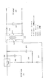
図1は、本発明の教示によるスイッチ・モード電源の一実施形態の概略図を示す。この概略図に示したすべての回路を使用して、パワーMOSFET2のスイッチングを制御する。スイッチングのタイミングは発振器5によって制御される。発振器5は、クロック10、DMAX(最大デューティ・サイクル)15、および鋸波20の3つの信号を生成する。クロック信号10の立ち上がりエッジは、スイッチング・サイクルの開始を決定する。例示した実施形態に示したように、クロック信号10がハイのとき、出力ラッチ90がセットされ、これにより、パワーMOSFET2が導電を開始するように、出力ラッチ90から制御信号が出力される。最大導電時間は、ハイとなっているDMAX15信号によって決定される。DMAX15信号がローになるとラッチ90はリセットされ、したがって、パワーMOSFET2が導電することを不可能にするために、ラッチ90から制御信号が出力される。
【0017】
固有電流リミットは、ノード22上の電圧に一次比例する。前述したように、本発明の目的は、スイッチング・サイクルの経過時間に比例する固有電流リミットを生成することである。鋸波形20を使用して、このタスクを実施することができる。NTNトランジスタ30のベース電圧が上昇するとエミッタの電圧も、同じレートで上昇する。したがって、抵抗25を通過する電流は、スイッチング・サイクル中、時間の経過と共に線形に増加する。電流ミラー40によってこの電流をミラーリングした後、(時間の経過と共に)線形に増加する電流源27が誘導される。したがって、電流リミット閾値22は、線形に増加する電流源27と抵抗17を有する一定電流源50の組合わせの積に比例する。ノード37の電圧は、抵抗55と60によって形成された電圧分割器ネットワークのために、パワーMOSFETドレイン電圧に比例する。このドレイン電流はドレイン電圧に比例する。ドレイン電流7が、スイッチング・サイクル中にランプ・アップする際に、ノード37上の電圧は、比例して上昇する。ノード37上の電圧が電流リミット閾値ノード22の電圧を超えた後、コンパレータ70は、最終的にラッチをリセット90することによって、パワーMOSFETを不可能にする。
【0018】
PWMコンパレータ32は、電源の出力から来るフィードバック信号に基づいて、デューティ・サイクルを変化させる。フィードバック電圧が高くなるにつれ、デューティ・サイクルも高くなる。
【0019】
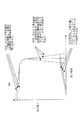
図2は、鋸波20、最大デューティ・サイクル15、および固有電流リミット22の3つの波形の実施形態を示す。鋸波形20と最大デューティ・サイクル波形15は発振器5によって生成される。最大デューティ・サイクル15信号は、パワーMOSFETスイッチング・サイクルがハイの時のその最大持続期間を決定する。鋸波形20は、最大デューティ・サイクル波形15がハイになるとき、低い点から増加し始める。これは、パワーMOSFETスイッチング・サイクルの開始の合図である。鋸波20の高い点には、サイクルの終了時に到達し、同時に、最大デューティ・サイクル信号15はローになる。固有電流リミット22信号は、サイクルの開始時に、低い点から開始してサイクルを通して時間の経過と共に線形に増加する。経過時間がゼロでは、固有電流リミットは、K1にある。経過時間が増加するにつれ、電流リミットは、K2×telapsed倍に増加する。したがって、図2からわかるように、固有電流リミット(ILIM-INTRINSIC)は、K1とK2×telapsedの和である。
【0020】
図3は、本発明の教示による、ほぼ一定な電圧とほぼ一定な電流の特性を有する電源の一実施形態を示す。エネルギー転送要素220は、DC出力200と高電圧DC入力255の間に結合される。一実施形態では、エネルギー転送要素は、入力巻線225と出力巻線215を含む変圧器である。レギュレーション回路250は、高電圧DC入力255とエネルギー転送要素220の間に結合され、DC出力200をレギュレートする。示した実施形態では、DC出力200に応答するフィードバック情報が、制御ピンのレギュレータ250に提供される。制御ピンの電流は、DC出力200の出力電圧に関係付けられる、抵抗235両端間の電圧に比例する。
【0021】
動作時には、レギュレータ回路は、抵抗235両端間の電圧が閾値より高くなるとき、パワーMOSFETのデューティ・サイクルを減少させる。この部分では出力はほぼ一定な電圧モードにある。レギュレータ回路は、抵抗235両端間の電圧が閾値より低くなるとき、パワーMOSFETの電流リミットを減少させる。電流リミットは、出力負荷電流を一定に保つために、抵抗235両端間の電圧の関数として減少する。したがって、負荷電流はレギュレータ250におけるパワーMOSFETの電流リミットに比例する。電流リミットを線間電圧に対し不変に保つことによって、出力負荷電流は、すべての線間電圧において、一定のままとなる。
【0022】
図4は、本発明の教示による、ほぼ一定な電圧とほぼ一定な電流の特性を有する電源の一実施形態を示す。フィードバック情報は、制御ピンのレギュレータ350に提供される。制御ピンの電流は、出力電圧に関係付けられる、抵抗335両端間の電圧に比例する。レギュレータ回路は、抵抗335両端間の電圧が、閾値より大きくなるとき、パワーMOSFETのデューティ・サイクルを減少させる。この部分では、出力はほぼ一定な電圧モードにある。レギュレータ回路は、抵抗335両端間の電圧が閾値より低くなるとき、パワーMOSFETの電流リミットを低減する。電流リミットは、出力負荷電流をほぼ一定に保つために、抵抗335を横切る電流の関数として減少される。したがって、負荷電流は、レギュレータ350にあるパワーMOSFETの電流リミットに比例する。電流リミットを線間電圧に関してほぼ一定に保つことによって、出力負荷電流は、すべての線間電圧において、ほぼ一定なままとなる。
【0023】
図5は、本発明の教示による電源の一実施形態の出力電流と出力電圧の通常の関係を示す図である。曲線400からわかるように、本発明を使用する電源は、ほぼ一定の出力電流とほぼ一定の出力電圧の特性を示す。すなわち、出力電流が増加する際、出力電流が出力電流閾値に到達するまで、出力電圧はほぼ一定なままである。出力電流が出力電流閾値に近づくと、出力電圧の降下の間出力電流がほぼ一定のまま出力電圧が減少し、より低い出力電圧閾値に到達すると、特性範囲で示したように出力電流も減少する。本発明の一定の出力電圧と一定の出力電流の特性は、電池充電器の応用などに適していることを理解されたい。
【0024】
以上の詳細な記述において、特有の例示的な実施形態を参照して、本発明の方法および装置を記述した。しかし、本発明のより広範な精神および範囲から逸脱せずに、様々な修正および変更を実施することが可能であることが明らかであろう。したがって、本明細書と図は、限定的ではなく、例示であると見なされるべきである。
【図面の簡単な説明】
【図1】本発明の教示によるスイッチ・モード電源レギュレータの一実施形態の概略図である。
【図2】本発明の教示による鋸波形、デューティ・サイクルの波形、および固有電流リミット波形の一実施形態を示す図である。
【図3】本発明の教示によるほぼ一定な電圧とほぼ一定な電流の特性を有する電源の一実施形態の図である。
【図4】本発明の教示によるほぼ一定な電圧とほぼ一定な電流の特性を有する電源の一実施形態の図である。
【図5】本発明の教示による電源の一実施形態の出力電流と出力電圧との通常の関係を示す図である。
【符号の説明】
2 パワーMOSFET(金属酸化物電界効果トランジスタ)
5 発振器
7 ドレイン電流
10 クロック信号
15 最大デューティ・サイクル信号(最大デューティ・サイクル波形)
17、25、55、60、235 抵抗
20 鋸波信号(鋸波形)
22、37 ノード
22 固有電流リミット閾値
27 線形に増加する電流源
30 NTNトランジスタ
32 PWMコンパレータ
40 電流ミラー
50 一定な電流源
70 コンパレータ
90 出力ラッチ
200 DC出力
215 出力巻線
225 入力巻線
220 エネルギー転送要素
250、350、335 レギュレータ
400 曲線[0001]
This application is filed on September 27, 2001, “Method And Apparatus For Maintaining A Constant Load Current With Line Voltage Int. No. 64 / U.S. App. Claim priority.
[0002]
BACKGROUND OF THE INVENTION
The present invention relates generally to power supplies, and more specifically, the invention relates to switch mode power supplies.
[0003]
[Prior art]
All electronic devices use power to operate. A mode of power supply that is highly efficient and at the same time acceptablely regulates the output to power an electronic device or other load is a switch mode power supply. Many electronic device applications, particularly the low power offline adapter / charger market, require a nearly constant output voltage below the output current threshold over the normal operating load of the power supply. The current output is generally regulated below an output voltage within this range of a substantially constant output voltage (hereinafter referred to as output voltage threshold).
[0004]
In known switch mode power supplies without a second current sensing circuit, minimizing the change in output current at the output voltage threshold is implemented by a complex control scheme. These schemes typically include measurements of input voltage, output diode conduction time, and peak primary current limit. Some or all of this measurement information is then used to control the regulator to reduce the change in output current at the output voltage threshold.
[0005]
[Means for Solving the Problems]
Disclosed is a power supply that maintains a substantially constant load current having a line voltage below an output voltage threshold. In one embodiment, the regulation circuit includes a semiconductor switch and a current sensing circuit that senses a current in the semiconductor switch. The current sensing circuit has a current limit threshold. The current limit threshold of the regulation circuit changes from the first level to the second level during the time when the semiconductor switch is on. In one embodiment, the regulation circuit is used in a power supply having an output characteristic having a substantially constant output voltage at a current below an output current threshold and a substantially constant output current at a voltage below the output voltage threshold. In another embodiment, a power supply is described that includes a power input and a power output and maintains a substantially constant load current having a line voltage below an output voltage threshold. In one embodiment, the power supply has an output characteristic that has a substantially constant output voltage at a current below the output current threshold and a substantially constant output current at a voltage below the output voltage threshold. A regulation circuit is coupled between the power input and the power output. The regulation circuit includes a semiconductor switch and a current sensing circuit that senses a current of the semiconductor switch. The current sensing circuit has a current limit threshold. The current limit threshold of the regulation circuit changes from the first level to the second level during the time when the semiconductor switch is on. In another aspect, the reached current limit threshold is consistent with a power output characteristic that transitions from providing a substantially constant output voltage to providing a substantially constant output current. In another aspect, the semiconductor switch is a MOSFET. Additional features and advantages of the present invention will become apparent from the detailed description and figures set forth below.
[0006]
The invention is illustrated in detail in the accompanying figures by way of example and not limitation.
[0007]
DETAILED DESCRIPTION OF THE INVENTION
A method for keeping the output current of a power supply substantially constant regardless of the input voltage at the point where the output characteristics of the power supply shift from providing a substantially constant output voltage to supplying a substantially constant output current. And apparatus embodiments are disclosed. In the following description, certain specific details are set forth in order to provide a thorough understanding of the present invention. However, it will be apparent to those skilled in the art that the specific details need not be used to implement the present invention. In other instances, well-known materials or methods have not been described in order to avoid obscuring the present invention.
[0008]
Throughout this specification, reference to “one embodiment” or “an embodiment” means that a particular feature, structure, or characteristic described with respect to the embodiment is included in at least one embodiment of the invention. . Thus, the appearances of the phrases “in one embodiment” or “in an embodiment” in various places throughout this specification are not necessarily all referring to the same embodiment. Furthermore, the particular features, structures, or characteristics may be included in one or more embodiments in a suitable manner.
[0009]
Now, in one embodiment, a switch mode power supply is described in which the output current at a voltage below the output voltage threshold is regulated to be substantially constant. This provides a substantially constant voltage / constant current output characteristic. The output current level of the output voltage threshold at a known power supply is sensed at the output of the power supply to provide feedback to a regulator circuit coupled to the primary winding of the power supply. However, if a nearly constant current function is achieved without feedback from the secondary winding of the power supply, the output current at the output voltage threshold is a function of the primary regulator peak current limit.
[0010]
Embodiments of the present invention reduce the change in output current at the output voltage threshold by changing the input voltage to reduce the change in peak current limit. Usually, the intrinsic peak limiting current is set to be constant by the internal circuit of the regulator. In one embodiment, the switching cycle should theoretically be terminated immediately after the drain current reaches the current limit threshold. However, there is an inherent fixed delay from when the threshold is reached until the power metal oxide semiconductor field effect semiconductor (MOSFET) is eventually disabled. During this delay, the drain current continues to ramp up at a rate equal to the direct current (DC) input voltage divided by the primary inductance of the transformer (drain current ramp rate). Therefore, the actual current limit is the sum of the intrinsic current limit threshold and the ramp rate dependent component (overshoot), which is the drain current ramp rate multiplied by a fixed delay. Thus, at higher DC input voltages, the actual current limit ramps to a higher level above the intrinsic current limit level than at lower DC input voltages. This can result in a change in output current delivered to the output voltage threshold load over a range of input line voltages.
[0011]
The actual current limit is the sum of the intrinsic current limit and the ramp rate dependent component (overshoot). The objective is to maintain a constant actual current limit over changes in the DC input voltage. Since the ramp rate component (overshoot) increases with DC input voltage, the only way to maintain a relatively constant current limit is to reduce the intrinsic current limit threshold as the DC input voltage rises. .
[0012]
In a discontinuous power supply design, the point at which the current limit in time during the switching cycle is reached depends on the DC input voltage. In fact, the time taken from the start of the cycle to the point where the current limit is reached is inversely proportional to the DC input voltage. Thus, the DC input voltage can be measured using the time elapsed since the start of the cycle.
[0013]
Thus, the elapsed time can be used to create a specific current limit that decreases with respect to the DC input voltage. It is only necessary to increase the intrinsic current limit as a function of the elapsed time during the cycle. A first approximation to the intrinsic current limit that increases with time is obtained by using
I LIM-INTRINSIC = K 1 + K 2 × t elapsed (Formula 1)
Where I LIM-INTRINSIC is the intrinsic current limit, K 1 and K 2 are constant values, and t elapsed is the elapsed time.
[0014]
In one embodiment, the elapsed time can be detected by the output waveform of the internal oscillator. In one embodiment, the waveform is a triangular waveform. This starts from the minimum at the start of the cycle and ramps gradually until the maximum duty cycle point is reached.
[0015]
In one embodiment, the ramp is approximately linear with respect to time. In other embodiments, the lamp may be non-linear depending on the requirements of the power source in which the regulator is used. The intrinsic current limit threshold is basically proportional to the voltage appearing at the input of the current limit comparator. This bias voltage is the product of the resistance value and the current sent to this resistor. Thus, one way to increase the intrinsic current limit linearly as a function of elapsed time is to derive a linearly increasing (relative to elapsed time) current source and send that current to the resistor. Thus, this linearly increasing current source (with respect to elapsed time) can be obtained from the oscillator.
[0016]
FIG. 1 shows a schematic diagram of one embodiment of a switch mode power supply in accordance with the teachings of the present invention. All the circuits shown in this schematic are used to control the switching of the
[0017]
The intrinsic current limit is linearly proportional to the voltage on
[0018]
The
[0019]
FIG. 2 shows three waveform embodiments: sawtooth 20,
[0020]
FIG. 3 illustrates one embodiment of a power supply having substantially constant voltage and substantially constant current characteristics in accordance with the teachings of the present invention. The
[0021]
In operation, the regulator circuit reduces the duty cycle of the power MOSFET when the voltage across
[0022]
FIG. 4 illustrates one embodiment of a power supply having substantially constant voltage and substantially constant current characteristics in accordance with the teachings of the present invention. The feedback information is provided to the
[0023]
FIG. 5 is a diagram illustrating the normal relationship between output current and output voltage for one embodiment of a power supply in accordance with the teachings of the present invention. As can be seen from
[0024]
In the foregoing detailed description, the method and apparatus of the present invention have been described with reference to specific exemplary embodiments. However, it will be apparent that various modifications and changes can be made without departing from the broader spirit and scope of the invention. The specification and drawings are accordingly to be regarded in an illustrative rather than restrictive sense.
[Brief description of the drawings]
FIG. 1 is a schematic diagram of one embodiment of a switch mode power supply regulator in accordance with the teachings of the present invention.
FIG. 2 illustrates one embodiment of a sawtooth waveform, a duty cycle waveform, and a natural current limit waveform in accordance with the teachings of the present invention.
FIG. 3 is a diagram of one embodiment of a power supply having approximately constant voltage and substantially constant current characteristics in accordance with the teachings of the present invention.
FIG. 4 is a diagram of one embodiment of a power supply having substantially constant voltage and substantially constant current characteristics in accordance with the teachings of the present invention.
FIG. 5 is a diagram illustrating the normal relationship between output current and output voltage for one embodiment of a power supply in accordance with the teachings of the present invention.
[Explanation of symbols]
2 Power MOSFET (Metal Oxide Field Effect Transistor)
5
17, 25, 55, 60, 235
22, 37
Claims (19)
前記スイッチに結合され、スイッチの電流を感知する電流感知回路とを有し、
この電流感知回路は、前記スイッチがオンである時間の間に第1レベルから第2レベルに増加する可変電流リミット閾値を有し、前記制御信号は、前記電流感知回路の出力に応答して、電源出力に出力電圧閾値より低い電圧でほぼ一定の出力電流を有する出力特性を提供し、前記可変電流リミット閾値は前記スイッチの前記第1端子と前記第2端子間に結合される前記電流のリミット閾値を可変にセットする電源レギュレーション回路。A switch including a first terminal, a second terminal, and a control terminal, wherein the switch is operable to couple or separate the first terminal and the second terminal in response to a control signal received at the control terminal;
A current sensing circuit coupled to the switch for sensing a switch current ;
The current sensing circuit includes a variable current limit threshold is increased from a first level to a second level during the time the switch is on, the control signal is responsive to an output of the current sensing circuit, It provides an output characteristic having a substantially constant output current at a voltage lower than the output voltage threshold to a power supply output, the variable current limit threshold limit of the current that is coupled between the first terminal and the second terminal of the switch Power supply regulation circuit that variably sets the threshold .
電源入力とエネルギー転送要素との間に結合されたレギュレーション回路とを備え、レギュレーション回路が
電源出力へエネルギーを送るのを制御するために、電源入力とエネルギー転送要素との間に結合されたスイッチング・デバイスと、
前記スイッチング・デバイスに結合され、スイッチング・デバイスの電流を感知する電流感知回路であって、この電流感知回路は、電源出力が出力電圧閾値より低い電圧でほぼ一定の出力電流を有する出力特性を提供すべくレギュレートされるように、前記スイッチング・デバイスがオンである時間の間に第1レベルから第2レベルに増加する可変電流リミット閾値を有し、前記可変電流リミット閾値は前記電源入力と前記エネルギー転送要素間に結合される前記電流のリミット閾値を可変にセットする電源。An energy transfer element coupled between the power input and the power output;
A switching circuit coupled between the power input and the energy transfer element to control the regulation circuit delivering energy to the power output. The device,
A current sensing circuit coupled to the switching device and sensing a current of the switching device , wherein the current sensing circuit provides an output characteristic having a substantially constant output current at a voltage lower than an output voltage threshold. as regulated so as to, the switching device have a variable current limit threshold is increased from a first level during the time that is on the second level, the variable current limit threshold and the power supply input said A power supply that variably sets a limit threshold for the current coupled between energy transfer elements .
制御信号に応答して、スイッチング・デバイスで、電源入力から電源出力へのエネルギーの流れを可能または不可能にすることと、
スイッチング・デバイスを通る電流を感知することと、
スイッチング・デバイスを通る電流が可変電流リミット閾値に到達するのに応答して、スイッチング・デバイスを不能、即ち、非導通にすることと、
電源出力が、出力電圧閾値より低い電圧でほぼ一定の出力電流を有する出力特性を提供すべくレギュレートされるように、スイッチング・デバイスがオンである時間の間に第1レベルから第2レベルに、可変電流リミット閾値を増やすこととを備える方法。A method of regulating a power supply,
In response to the control signal, enabling or disabling the flow of energy from the power input to the power output at the switching device;
Sensing the current through the switching device;
In response to the current through the switching device reaching a variable current limit threshold, disabling the switching device;
Power output, as regulated to provide an output characteristic having an approximately constant output current lower than the output voltage threshold voltage, the second level from the first level during the time the switching device is on Increasing the variable current limit threshold.
鋸波形を生成することと、
鋸波形の変化に従って変化する可変電流リミット閾値を得ることとを含む請求項14に記載の方法。 Increasing the variable current limit threshold between the first level and the second level is
Generating a sawtooth waveform;
15. The method of claim 14, comprising obtaining a variable current limit threshold that varies according to a change in the sawtooth waveform.
スイッチング・デバイスを不可能、即ち、非導通にすることは、スイッチング・デバイスを通る電流が可変電流リミット閾値に到達するのに応答して前記ラッチをリセットすることを含む請求項14に記載の方法。 Further comprising providing a control signal from the latch;
Not switching devices, i.e., be non-conductive A method according to claim 14, in response to the current through the switching device reaches a variable current limit threshold includes resetting said latch .
Applications Claiming Priority (4)
| Application Number | Priority Date | Filing Date | Title |
|---|---|---|---|
| US32564201P | 2001-09-27 | 2001-09-27 | |
| US60/325,642 | 2001-09-27 | ||
| US10/253,307 | 2002-09-23 | ||
| US10/253,307 US6781357B2 (en) | 2001-09-27 | 2002-09-23 | Method and apparatus for maintaining a constant load current with line voltage in a switch mode power supply |
Publications (3)
| Publication Number | Publication Date |
|---|---|
| JP2003189612A JP2003189612A (en) | 2003-07-04 |
| JP2003189612A5 JP2003189612A5 (en) | 2005-10-27 |
| JP4293302B2 true JP4293302B2 (en) | 2009-07-08 |
Family
ID=26943121
Family Applications (1)
| Application Number | Title | Priority Date | Filing Date |
|---|---|---|---|
| JP2002284064A Expired - Fee Related JP4293302B2 (en) | 2001-09-27 | 2002-09-27 | Method and apparatus for maintaining a constant load current with line voltage in a switch mode power supply |
Country Status (3)
| Country | Link |
|---|---|
| US (7) | US6781357B2 (en) |
| EP (2) | EP2270965B1 (en) |
| JP (1) | JP4293302B2 (en) |
Families Citing this family (116)
| Publication number | Priority date | Publication date | Assignee | Title |
|---|---|---|---|---|
| US6781357B2 (en) | 2001-09-27 | 2004-08-24 | Power Integrations, Inc. | Method and apparatus for maintaining a constant load current with line voltage in a switch mode power supply |
| DE10245484B4 (en) * | 2002-09-30 | 2004-07-22 | Infineon Technologies Ag | Method for controlling a semiconductor switch and circuit arrangement with a semiconductor switch |
| US6963188B2 (en) * | 2004-04-06 | 2005-11-08 | Atmel Corporation | On-chip power supply interface with load-independent current demand |
| US7224154B2 (en) * | 2004-04-16 | 2007-05-29 | Dell Products L.P. | System and method for adjusting the current limit of a power supply |
| DE102004059960A1 (en) | 2004-12-13 | 2006-06-22 | Bourns, Inc., Riverside | Circuit arrangement for measuring an electric current |
| US7254044B2 (en) * | 2005-01-11 | 2007-08-07 | Artesyn Technologies, Inc. | Current limit circuit and power supply including same |
| US7265999B2 (en) | 2005-04-06 | 2007-09-04 | Matsushita Electric Industrial Co., Ltd. | Power supply regulator circuit and semiconductor device |
| US7593245B2 (en) | 2005-07-08 | 2009-09-22 | Power Integrations, Inc. | Method and apparatus to limit maximum switch current in a switching power supply |
| US7215107B2 (en) * | 2005-07-11 | 2007-05-08 | Power Integrations, Inc. | Method and apparatus to limit output power in a switching power supply |
| KR101247801B1 (en) * | 2005-10-25 | 2013-03-26 | 페어차일드코리아반도체 주식회사 | Switching mode power supply |
| US11881814B2 (en) | 2005-12-05 | 2024-01-23 | Solaredge Technologies Ltd. | Testing of a photovoltaic panel |
| US10693415B2 (en) | 2007-12-05 | 2020-06-23 | Solaredge Technologies Ltd. | Testing of a photovoltaic panel |
| GB2436155A (en) * | 2006-03-14 | 2007-09-19 | Cambridge Semiconductor Ltd | Switch mode power supply current sensing |
| GB2439998A (en) * | 2006-07-07 | 2008-01-16 | Cambridge Semiconductor Ltd | Estimating the output current of a switch mode power supply |
| GB2439997A (en) * | 2006-07-07 | 2008-01-16 | Cambridge Semiconductor Ltd | Estimating the output current of a switch mode power supply |
| US7576528B2 (en) * | 2006-10-04 | 2009-08-18 | Power Integrations, Inc. | Control circuit responsive to an impedance |
| US7518885B2 (en) * | 2006-10-04 | 2009-04-14 | Power Integrations, Inc. | Method and apparatus for a control circuit with multiple operation modes |
| US7502236B2 (en) * | 2006-10-04 | 2009-03-10 | Power Integrations, Inc. | Power supply controller responsive to a feedforward signal |
| US8319483B2 (en) | 2007-08-06 | 2012-11-27 | Solaredge Technologies Ltd. | Digital average input current control in power converter |
| US11855231B2 (en) | 2006-12-06 | 2023-12-26 | Solaredge Technologies Ltd. | Distributed power harvesting systems using DC power sources |
| US9088178B2 (en) | 2006-12-06 | 2015-07-21 | Solaredge Technologies Ltd | Distributed power harvesting systems using DC power sources |
| US11569659B2 (en) | 2006-12-06 | 2023-01-31 | Solaredge Technologies Ltd. | Distributed power harvesting systems using DC power sources |
| US8618692B2 (en) | 2007-12-04 | 2013-12-31 | Solaredge Technologies Ltd. | Distributed power system using direct current power sources |
| US8947194B2 (en) | 2009-05-26 | 2015-02-03 | Solaredge Technologies Ltd. | Theft detection and prevention in a power generation system |
| US8384243B2 (en) | 2007-12-04 | 2013-02-26 | Solaredge Technologies Ltd. | Distributed power harvesting systems using DC power sources |
| US9112379B2 (en) | 2006-12-06 | 2015-08-18 | Solaredge Technologies Ltd. | Pairing of components in a direct current distributed power generation system |
| US11296650B2 (en) | 2006-12-06 | 2022-04-05 | Solaredge Technologies Ltd. | System and method for protection during inverter shutdown in distributed power installations |
| US11687112B2 (en) | 2006-12-06 | 2023-06-27 | Solaredge Technologies Ltd. | Distributed power harvesting systems using DC power sources |
| US11728768B2 (en) | 2006-12-06 | 2023-08-15 | Solaredge Technologies Ltd. | Pairing of components in a direct current distributed power generation system |
| US11309832B2 (en) | 2006-12-06 | 2022-04-19 | Solaredge Technologies Ltd. | Distributed power harvesting systems using DC power sources |
| US8319471B2 (en) | 2006-12-06 | 2012-11-27 | Solaredge, Ltd. | Battery power delivery module |
| US8473250B2 (en) | 2006-12-06 | 2013-06-25 | Solaredge, Ltd. | Monitoring of distributed power harvesting systems using DC power sources |
| US8816535B2 (en) | 2007-10-10 | 2014-08-26 | Solaredge Technologies, Ltd. | System and method for protection during inverter shutdown in distributed power installations |
| US11735910B2 (en) | 2006-12-06 | 2023-08-22 | Solaredge Technologies Ltd. | Distributed power system using direct current power sources |
| US8013472B2 (en) | 2006-12-06 | 2011-09-06 | Solaredge, Ltd. | Method for distributed power harvesting using DC power sources |
| US8963369B2 (en) | 2007-12-04 | 2015-02-24 | Solaredge Technologies Ltd. | Distributed power harvesting systems using DC power sources |
| US11888387B2 (en) | 2006-12-06 | 2024-01-30 | Solaredge Technologies Ltd. | Safety mechanisms, wake up and shutdown methods in distributed power installations |
| US9130401B2 (en) | 2006-12-06 | 2015-09-08 | Solaredge Technologies Ltd. | Distributed power harvesting systems using DC power sources |
| US8077483B2 (en) | 2007-04-06 | 2011-12-13 | Power Integrations, Inc. | Method and apparatus for sensing multiple voltage values from a single terminal of a power converter controller |
| KR101365752B1 (en) * | 2007-04-19 | 2014-02-21 | 페어차일드코리아반도체 주식회사 | Switching mode power supply and switch thereof |
| US8289731B2 (en) * | 2007-06-05 | 2012-10-16 | O2Micro Inc. | Converter controller |
| TW200849779A (en) * | 2007-06-13 | 2008-12-16 | Richtek Technology Corp | Method and device to limit the output power of switching-type converter |
| JP5657853B2 (en) * | 2007-10-02 | 2015-01-21 | ピーエスフォー ルクスコ エスエイアールエルPS4 Luxco S.a.r.l. | Constant current source circuit |
| US8451627B2 (en) * | 2007-11-16 | 2013-05-28 | Itron, Inc. | Devices and methods for converting alternating current (AC) power to direct current (DC) power |
| DE102007058314B4 (en) * | 2007-12-04 | 2018-11-15 | Diehl Aerospace Gmbh | Device for measuring a load current |
| US8289742B2 (en) | 2007-12-05 | 2012-10-16 | Solaredge Ltd. | Parallel connected inverters |
| US8049523B2 (en) | 2007-12-05 | 2011-11-01 | Solaredge Technologies Ltd. | Current sensing on a MOSFET |
| US11264947B2 (en) | 2007-12-05 | 2022-03-01 | Solaredge Technologies Ltd. | Testing of a photovoltaic panel |
| WO2009072075A2 (en) | 2007-12-05 | 2009-06-11 | Solaredge Technologies Ltd. | Photovoltaic system power tracking method |
| EP3496258A1 (en) | 2007-12-05 | 2019-06-12 | Solaredge Technologies Ltd. | Safety mechanisms in distributed power installations |
| EP2269290B1 (en) | 2008-03-24 | 2018-12-19 | Solaredge Technologies Ltd. | Switch mode converter including active clamp for achieving zero voltage switching |
| EP2294669B8 (en) | 2008-05-05 | 2016-12-07 | Solaredge Technologies Ltd. | Direct current power combiner |
| TWI382636B (en) * | 2008-06-06 | 2013-01-11 | Richtek Technology Corp | And a control method and a device for controlling the maximum output power of the power supply |
| JP2010041832A (en) * | 2008-08-06 | 2010-02-18 | Panasonic Corp | Switching power supply controller and semiconductor apparatus used for the same |
| JP2010124572A (en) * | 2008-11-19 | 2010-06-03 | Panasonic Corp | Switching power supply |
| KR101530358B1 (en) * | 2009-02-05 | 2015-06-22 | 페어차일드코리아반도체 주식회사 | Switch control device and switch control method |
| US20120044724A1 (en) * | 2009-04-27 | 2012-02-23 | Panasonic Corporation | Switching power supply apparatus |
| CN101562397B (en) * | 2009-05-27 | 2014-02-12 | 成都芯源系统有限公司 | Dual-mode constant current control method based on third winding detection and circuit thereof |
| JP2011015557A (en) * | 2009-07-02 | 2011-01-20 | Panasonic Corp | Switching power supply apparatus, and semiconductor device for control of the same |
| US8228027B2 (en) * | 2009-10-13 | 2012-07-24 | Multi-Fineline Electronix, Inc. | Wireless power transmitter with multilayer printed circuit |
| US8710699B2 (en) | 2009-12-01 | 2014-04-29 | Solaredge Technologies Ltd. | Dual use photovoltaic system |
| US8213192B2 (en) * | 2009-12-30 | 2012-07-03 | Silicon Laboratories Inc. | Primary side sensing for isolated fly-back converters |
| US8797011B2 (en) * | 2010-01-08 | 2014-08-05 | General Electric Company | Variable current limiter for regulator |
| US8766696B2 (en) | 2010-01-27 | 2014-07-01 | Solaredge Technologies Ltd. | Fast voltage level shifter circuit |
| US8773869B2 (en) * | 2010-03-29 | 2014-07-08 | Itron, Inc. | System and method for conversion of high voltage AC to low voltage DC using input voltage gating |
| JP2011229327A (en) * | 2010-04-22 | 2011-11-10 | Toyota Central R&D Labs Inc | Switching control circuit |
| GB2485527B (en) | 2010-11-09 | 2012-12-19 | Solaredge Technologies Ltd | Arc detection and prevention in a power generation system |
| US10230310B2 (en) | 2016-04-05 | 2019-03-12 | Solaredge Technologies Ltd | Safety switch for photovoltaic systems |
| US10673229B2 (en) | 2010-11-09 | 2020-06-02 | Solaredge Technologies Ltd. | Arc detection and prevention in a power generation system |
| US10673222B2 (en) | 2010-11-09 | 2020-06-02 | Solaredge Technologies Ltd. | Arc detection and prevention in a power generation system |
| GB2486408A (en) | 2010-12-09 | 2012-06-20 | Solaredge Technologies Ltd | Disconnection of a string carrying direct current |
| TWI411205B (en) * | 2010-12-10 | 2013-10-01 | Richtek Technology Corp | Current sense circuit for a switch mode power supply |
| GB2483317B (en) | 2011-01-12 | 2012-08-22 | Solaredge Technologies Ltd | Serially connected inverters |
| CN102185478A (en) * | 2011-05-25 | 2011-09-14 | 无锡新硅微电子有限公司 | Circuit structure for automatically adjusting output voltage of peak current circuit |
| EP2533612A1 (en) | 2011-06-10 | 2012-12-12 | Exscitron GmbH | LED power supply for standby control mode |
| US8570005B2 (en) | 2011-09-12 | 2013-10-29 | Solaredge Technologies Ltd. | Direct current link circuit |
| US9048747B2 (en) | 2011-11-23 | 2015-06-02 | Zahid Ansari | Switched-mode power supply startup circuit, method, and system incorporating same |
| GB2498365A (en) | 2012-01-11 | 2013-07-17 | Solaredge Technologies Ltd | Photovoltaic module |
| US9853565B2 (en) | 2012-01-30 | 2017-12-26 | Solaredge Technologies Ltd. | Maximized power in a photovoltaic distributed power system |
| GB2498791A (en) | 2012-01-30 | 2013-07-31 | Solaredge Technologies Ltd | Photovoltaic panel circuitry |
| GB2498790A (en) | 2012-01-30 | 2013-07-31 | Solaredge Technologies Ltd | Maximising power in a photovoltaic distributed power system |
| GB2499991A (en) | 2012-03-05 | 2013-09-11 | Solaredge Technologies Ltd | DC link circuit for photovoltaic array |
| US9870016B2 (en) | 2012-05-25 | 2018-01-16 | Solaredge Technologies Ltd. | Circuit for interconnected direct current power sources |
| US10115841B2 (en) | 2012-06-04 | 2018-10-30 | Solaredge Technologies Ltd. | Integrated photovoltaic panel circuitry |
| US8887119B2 (en) * | 2013-03-12 | 2014-11-11 | Analog Devices Technology | Method and apparatus for current limit test for high power switching regulator |
| US9246392B2 (en) | 2013-03-13 | 2016-01-26 | Power Integrations, Inc. | Switched mode power converter controller with ramp time modulation |
| US9941813B2 (en) | 2013-03-14 | 2018-04-10 | Solaredge Technologies Ltd. | High frequency multi-level inverter |
| US9548619B2 (en) | 2013-03-14 | 2017-01-17 | Solaredge Technologies Ltd. | Method and apparatus for storing and depleting energy |
| EP3506370B1 (en) | 2013-03-15 | 2023-12-20 | Solaredge Technologies Ltd. | Bypass mechanism |
| WO2015070923A1 (en) | 2013-11-15 | 2015-05-21 | Advantest Corporation | Tester |
| WO2015070924A1 (en) | 2013-11-15 | 2015-05-21 | Advantest Corporation | Tester |
| WO2015081980A1 (en) | 2013-12-02 | 2015-06-11 | Advantest Corporation | Instruction provider and method for providing a sequence of instructions, test processor and method for providing a device under test |
| WO2015090425A1 (en) * | 2013-12-19 | 2015-06-25 | Advantest Corporation | A power supply device, a test equipment comprising a power supply device and a method for operating a power supply device |
| WO2015090478A1 (en) | 2013-12-20 | 2015-06-25 | Advantest Corporation | Multi-port measurement technique for determining s-parameters |
| DE102014201584A1 (en) * | 2014-01-29 | 2015-07-30 | Robert Bosch Gmbh | Semiconductor switch and method for determining a current through a semiconductor switch |
| KR20160114693A (en) | 2014-01-30 | 2016-10-05 | 주식회사 아도반테스토 | Test apparatus and method for testing a device under test |
| US9318974B2 (en) | 2014-03-26 | 2016-04-19 | Solaredge Technologies Ltd. | Multi-level inverter with flying capacitor topology |
| JP6410554B2 (en) | 2014-10-21 | 2018-10-24 | ローム株式会社 | Switching converter and its control circuit, AC / DC converter, power adapter and electronic device |
| WO2016066191A1 (en) | 2014-10-29 | 2016-05-06 | Advantest Corporation | Scheduler |
| US9680383B2 (en) * | 2014-11-07 | 2017-06-13 | Power Integrations, Inc. | Input overvoltage protection using current limit |
| WO2016082899A1 (en) | 2014-11-28 | 2016-06-02 | Advantest Corporation | Removal of sampling clock jitter induced in an output signal of an analog-to-digital converter |
| WO2016102020A1 (en) | 2014-12-23 | 2016-06-30 | Advantest Corporation | Test equipment, method for operating a test equipment and computer program |
| WO2016155830A1 (en) | 2015-04-01 | 2016-10-06 | Advantest Corporation | Method for operating a test apparatus and a test apparatus |
| WO2016173619A1 (en) | 2015-04-27 | 2016-11-03 | Advantest Corporation | Switch circuit, method for operating a switch circuit and an automated test equipment |
| WO2016188572A1 (en) | 2015-05-27 | 2016-12-01 | Advantest Corporation | Automated test equipment for combined signals |
| WO2016198100A1 (en) | 2015-06-10 | 2016-12-15 | Advantest Corporation | High frequency integrated circuit and emitting device for irradiating the integrated circuit |
| CN107153212B (en) | 2016-03-03 | 2023-07-28 | 太阳能安吉科技有限公司 | Method for mapping a power generation facility |
| US11081608B2 (en) | 2016-03-03 | 2021-08-03 | Solaredge Technologies Ltd. | Apparatus and method for determining an order of power devices in power generation systems |
| US10599113B2 (en) | 2016-03-03 | 2020-03-24 | Solaredge Technologies Ltd. | Apparatus and method for determining an order of power devices in power generation systems |
| US11177663B2 (en) | 2016-04-05 | 2021-11-16 | Solaredge Technologies Ltd. | Chain of power devices |
| US11018623B2 (en) | 2016-04-05 | 2021-05-25 | Solaredge Technologies Ltd. | Safety switch for photovoltaic systems |
| US10205394B2 (en) * | 2016-09-16 | 2019-02-12 | Power Integrations, Inc. | Switched mode power converter controller with ramp time modulation with jitter frequency |
| US10243442B1 (en) | 2017-11-22 | 2019-03-26 | Power Integrations, Inc. | Controller with frequency to on-time converter |
| US11418121B2 (en) | 2019-12-30 | 2022-08-16 | Power Integrations, Inc | Auxiliary converter to provide operating power for a controller |
| US11258369B2 (en) | 2020-02-19 | 2022-02-22 | Power Integrations, Inc. | Inductive charging circuit to provide operative power for a controller |
| CN113037069B (en) * | 2021-03-12 | 2022-07-15 | 杰华特微电子股份有限公司 | Switch protection circuit and power converter |
Family Cites Families (83)
| Publication number | Priority date | Publication date | Assignee | Title |
|---|---|---|---|---|
| US2922913A (en) * | 1958-11-19 | 1960-01-26 | Lester A Cushman | Lightning arrester |
| US3694772A (en) * | 1971-04-12 | 1972-09-26 | Information Storage Systems | Voltage control sawtooth oscillator with flyback time independent of frequency |
| JPS5353906Y2 (en) * | 1974-03-28 | 1978-12-23 | ||
| US3988661A (en) * | 1974-12-24 | 1976-10-26 | General Electric Company | Power supply system for generating constant power under maximum current conditions |
| US4032828A (en) * | 1976-04-12 | 1977-06-28 | Korhumel Industries, Inc. | Battery back-up system for electromagnets |
| US4238813A (en) * | 1979-05-21 | 1980-12-09 | The Bendix Corporation | Compensated dual injector driver |
| US4371824A (en) * | 1979-07-05 | 1983-02-01 | Eaton Corporation | Base drive and overlap protection circuit |
| US4293902A (en) | 1979-12-04 | 1981-10-06 | Ael Mirrotel, Ltd. | Transformerless fast current limiter with symetry correction for a switched-mode power supply |
| BE883739A (en) * | 1980-06-10 | 1980-10-01 | Organisation Europ De Rech S S | DEVICE FOR ADJUSTING AN OPERATING PARAMETER OF AN INSTALLATION |
| US4357572A (en) | 1981-03-26 | 1982-11-02 | Bell Telephone Laboratories, Incorporated | Current flare out limit control for PWM converter |
| DE3149526A1 (en) * | 1981-12-14 | 1983-06-23 | Philips Patentverwaltung | CIRCUIT ARRANGEMENT FOR OPERATING HIGH PRESSURE GAS DISCHARGE LAMPS |
| US4471283A (en) | 1982-11-02 | 1984-09-11 | International Business Machines Corporation | Average current regulation for stepper motors |
| CH657864A5 (en) * | 1984-02-17 | 1986-09-30 | Ciba Geigy Ag | WATER-SOLUBLE PHTHALOCYANINE COMPOUNDS AND THE USE THEREOF AS PHOTOACTIVATORS. |
| US4674020A (en) * | 1985-12-13 | 1987-06-16 | Siliconix Incorporated | Power supply having dual ramp control circuit |
| FR2596927B1 (en) | 1986-04-04 | 1988-05-20 | Thomson Csf | CUT-OFF POWER PROTECTION CIRCUIT |
| US4695920A (en) * | 1986-08-14 | 1987-09-22 | Geomation, Inc. | Isothermal cavity and spark gap protection assembly for input/output connection terminals for electronic modules |
| US4864618A (en) * | 1986-11-26 | 1989-09-05 | Wright Technologies, L.P. | Automated transaction system with modular printhead having print authentication feature |
| US4764856A (en) | 1987-01-23 | 1988-08-16 | U.S. Philips Corporation | Power-supply arrangement |
| GB8701558D0 (en) * | 1987-01-24 | 1987-02-25 | Pressac Ltd | Printed circuit connector |
| US4884982A (en) * | 1989-04-03 | 1989-12-05 | Amp Incorporated | Capacitive coupled connector |
| US4902957A (en) | 1989-04-27 | 1990-02-20 | International Business Machines Corporation | DC/DC converter |
| US5028861A (en) * | 1989-05-24 | 1991-07-02 | Motorola, Inc. | Strobed DC-DC converter with current regulation |
| US5045800A (en) * | 1990-03-23 | 1991-09-03 | Power Integrations, Inc. | Pulse width modulator control circuit |
| US5014178A (en) * | 1990-05-14 | 1991-05-07 | Power Integrations, Inc. | Self powering technique for integrated switched mode power supply |
| US5145526A (en) * | 1990-11-07 | 1992-09-08 | Hammer Metals Company, Inc. | Apparatus for facilitating the spraying of articles |
| JPH04175908A (en) | 1990-11-09 | 1992-06-23 | Mitsubishi Electric Corp | Switching regulator |
| JPH04281606A (en) | 1991-03-11 | 1992-10-07 | Matsushita Electric Ind Co Ltd | Pulse width modulation amplifier |
| US5261733A (en) * | 1991-05-29 | 1993-11-16 | The Yokohama Rubber Co., Ltd. | Shoe of crawler belt or chain |
| US5326260A (en) * | 1991-06-17 | 1994-07-05 | Klein Douglas J | Medical tool dispenser system and devices |
| US5189599A (en) | 1991-08-14 | 1993-02-23 | Zenith Electronics Corporation | High voltage regulator for an integrated horizontal sweep system |
| US5268631A (en) * | 1991-11-06 | 1993-12-07 | Chicago Stage Equipment Co. | Power control system with improved phase control |
| US5245526A (en) | 1992-02-07 | 1993-09-14 | Power Integrations, Inc. | Below ground current sensing with current input to control threshold |
| US5342210A (en) * | 1992-03-26 | 1994-08-30 | Intermec Corporation | Connector for a bar code scanner |
| US5852434A (en) * | 1992-04-03 | 1998-12-22 | Sekendur; Oral F. | Absolute optical position determination |
| US5477012A (en) * | 1992-04-03 | 1995-12-19 | Sekendur; Oral F. | Optical position determination |
| US5631444A (en) * | 1992-05-01 | 1997-05-20 | Daimler-Benz Aerospace Airbus Gmbh | Cable coupling for grounding an internal lightning protector device |
| US5215478A (en) * | 1992-05-29 | 1993-06-01 | Amphenol Corporation | Spark gap device |
| US5246388A (en) * | 1992-06-30 | 1993-09-21 | Amp Incorporated | Electrical over stress device and connector |
| US5313381A (en) * | 1992-09-01 | 1994-05-17 | Power Integrations, Inc. | Three-terminal switched mode power supply integrated circuit |
| US5285366A (en) * | 1992-09-24 | 1994-02-08 | Northern Telecom Limited | Current limit circuit in current mode power supplies |
| US5335162A (en) | 1993-01-15 | 1994-08-02 | Toko America, Inc. | Primary side controller for regulated power converters |
| DE69401965T2 (en) | 1993-01-21 | 1997-10-09 | Lambda Electronics Inc | Overload protection of a switching power supply |
| US5397250A (en) * | 1993-04-06 | 1995-03-14 | Amphenol Corporation | Modular jack with filter |
| JP3209249B2 (en) | 1993-07-29 | 2001-09-17 | 株式会社村田製作所 | Power supply |
| US5479090A (en) * | 1993-11-24 | 1995-12-26 | Raytheon Company | Power converter having optimal dynamic operation |
| EP0759219A4 (en) * | 1994-05-03 | 2000-12-20 | Electro Wire Products Inc | Power distribution module |
| US5528483A (en) * | 1994-08-23 | 1996-06-18 | Siliconix, Inc. | Voltage converter with frequency shift protection against overload current |
| FR2725324B1 (en) * | 1994-09-30 | 1996-12-20 | Sgs Thomson Microelectronics | CUT-OUT CURRENT REGULATOR |
| US5661506A (en) * | 1994-11-10 | 1997-08-26 | Sia Technology Corporation | Pen and paper information recording system using an imaging pen |
| US5724220A (en) * | 1994-12-08 | 1998-03-03 | Tii Industries, Inc. | Coaxial transmission line surge arrestor with fusible link |
| FI952571A (en) | 1995-05-26 | 1996-11-27 | Salcomp Oy | Method and circuit for checking output characteristics of a switched power supply |
| JP3500791B2 (en) | 1995-09-04 | 2004-02-23 | 松下電器産業株式会社 | Switching power supply |
| US5680034A (en) * | 1995-09-22 | 1997-10-21 | Toko, Inc. | PWM controller for resonant converters |
| US5674083A (en) * | 1995-11-22 | 1997-10-07 | The Whitaker Corporation | ESD protected electrical connector |
| US5692073A (en) * | 1996-05-03 | 1997-11-25 | Xerox Corporation | Formless forms and paper web using a reference-based mark extraction technique |
| US6036545A (en) * | 1996-11-27 | 2000-03-14 | The Whitaker Corporation | Decoupled BNC connector |
| US5820393A (en) * | 1996-12-30 | 1998-10-13 | Molex Incorporation | Board mounted electrical connector with multi-function board lock |
| US5729120A (en) * | 1996-12-30 | 1998-03-17 | General Signal Corporation | Dynamic voltage regulation stabilization for AC power supply systems |
| US6518950B1 (en) * | 1997-10-07 | 2003-02-11 | Interval Research Corporation | Methods and systems for providing human/computer interfaces |
| US6226190B1 (en) * | 1998-02-27 | 2001-05-01 | Power Integrations, Inc. | Off-line converter with digital control |
| DE19814681B4 (en) | 1998-04-01 | 2008-11-13 | Infineon Technologies Ag | Current Mode Switching Regulators |
| US5995386A (en) | 1998-04-03 | 1999-11-30 | Lucent Technologies Inc. | Control circuit arrangement for limiting output current in power switching transistor |
| US6037674A (en) * | 1998-06-26 | 2000-03-14 | Motorola, Inc. | Circuit and method of current limiting a half-bridge driver |
| US6964374B1 (en) * | 1998-10-02 | 2005-11-15 | Lucent Technologies Inc. | Retrieval and manipulation of electronically stored information via pointers embedded in the associated printed material |
| US6100667A (en) * | 1999-01-21 | 2000-08-08 | National Semiconductor Corporation | Current-to-voltage transition control of a battery charger |
| US6127815A (en) | 1999-03-01 | 2000-10-03 | Linear Technology Corp. | Circuit and method for reducing quiescent current in a switching regulator |
| DE19916915B4 (en) | 1999-04-14 | 2005-08-11 | Infineon Technologies Ag | Switching power supply and method for determining the supply voltage in a switched-mode power supply |
| US6154377A (en) * | 1999-10-08 | 2000-11-28 | Power Integrations, Inc. | Method and apparatus reducing overshoot in a power supply controller |
| US6526514B1 (en) * | 1999-10-11 | 2003-02-25 | Ati International Srl | Method and apparatus for power management interrupt processing in a computing system |
| US6233161B1 (en) | 2000-03-02 | 2001-05-15 | Power Integrations, Inc. | Switched mode power supply responsive to voltage across energy transfer element |
| US6498466B1 (en) | 2000-05-23 | 2002-12-24 | Linear Technology Corp. | Cancellation of slope compensation effect on current limit |
| US6333624B1 (en) | 2000-05-30 | 2001-12-25 | Semiconductor Components Industries Llc | Circuit and method for a switching power supply with primary side transformer sensing |
| US6525514B1 (en) * | 2000-08-08 | 2003-02-25 | Power Integrations, Inc. | Method and apparatus for reducing audio noise in a switching regulator |
| DE10040413B4 (en) * | 2000-08-18 | 2006-11-09 | Infineon Technologies Ag | Circuit arrangement for generating a switching signal for a current-controlled switching power supply |
| US6580593B2 (en) * | 2001-03-14 | 2003-06-17 | Power Integrations, Inc. | Method and apparatus for fault condition protection of a switched mode power supply |
| US6583994B2 (en) | 2001-06-19 | 2003-06-24 | Space Systems/Loral | Method and apparatus for soft switched AC power distribution |
| US6747443B2 (en) * | 2001-08-31 | 2004-06-08 | Power Integrations, Inc. | Method and apparatus for trimming current limit and frequency to maintain a constant maximum power |
| US6781357B2 (en) | 2001-09-27 | 2004-08-24 | Power Integrations, Inc. | Method and apparatus for maintaining a constant load current with line voltage in a switch mode power supply |
| US6833692B2 (en) * | 2002-01-17 | 2004-12-21 | Power Integrations, Inc. | Method and apparatus for maintaining an approximate constant current output characteristic in a switched mode power supply |
| US6674656B1 (en) | 2002-10-28 | 2004-01-06 | System General Corporation | PWM controller having a saw-limiter for output power limit without sensing input voltage |
| US7122076B2 (en) * | 2004-08-09 | 2006-10-17 | Silverbrook Research Pty Ltd | Synthetically expedient water-dispersible IR dyes |
| US7709633B2 (en) * | 2006-07-10 | 2010-05-04 | Silverbrook Research Pty Ltd | Ink formulations comprising gallium naphthalocyanines |
| US7658792B2 (en) * | 2006-07-10 | 2010-02-09 | Silverbrook Research Pty Ltd | Gallium naphthalocyanine salts for use as improved infrared dyes |
-
2002
- 2002-09-23 US US10/253,307 patent/US6781357B2/en not_active Expired - Lifetime
- 2002-09-27 JP JP2002284064A patent/JP4293302B2/en not_active Expired - Fee Related
- 2002-09-27 EP EP10184359.7A patent/EP2270965B1/en not_active Expired - Fee Related
- 2002-09-27 EP EP02256760A patent/EP1298778B1/en not_active Expired - Fee Related
-
2004
- 2004-07-15 US US10/892,300 patent/US7110270B2/en not_active Expired - Lifetime
-
2006
- 2006-04-03 US US11/397,524 patent/US7215105B2/en not_active Expired - Lifetime
-
2007
- 2007-04-06 US US11/784,560 patent/US7646184B2/en not_active Expired - Fee Related
-
2009
- 2009-10-16 US US12/581,054 patent/US7834605B2/en not_active Expired - Fee Related
-
2010
- 2010-10-13 US US12/904,015 patent/US8013584B2/en not_active Expired - Fee Related
-
2011
- 2011-07-28 US US13/193,284 patent/US8427124B2/en not_active Expired - Lifetime
Also Published As
| Publication number | Publication date |
|---|---|
| EP1298778B1 (en) | 2013-01-30 |
| US20070182394A1 (en) | 2007-08-09 |
| US8013584B2 (en) | 2011-09-06 |
| US7834605B2 (en) | 2010-11-16 |
| US7110270B2 (en) | 2006-09-19 |
| EP1298778A2 (en) | 2003-04-02 |
| US7646184B2 (en) | 2010-01-12 |
| US20110285374A1 (en) | 2011-11-24 |
| EP2270965A1 (en) | 2011-01-05 |
| US20040251886A1 (en) | 2004-12-16 |
| US20100033147A1 (en) | 2010-02-11 |
| US8427124B2 (en) | 2013-04-23 |
| EP2270965B1 (en) | 2013-07-10 |
| US20110025288A1 (en) | 2011-02-03 |
| US20060176716A1 (en) | 2006-08-10 |
| EP1298778A3 (en) | 2005-04-27 |
| US20030076078A1 (en) | 2003-04-24 |
| US7215105B2 (en) | 2007-05-08 |
| US6781357B2 (en) | 2004-08-24 |
| JP2003189612A (en) | 2003-07-04 |
Similar Documents
| Publication | Publication Date | Title |
|---|---|---|
| JP4293302B2 (en) | Method and apparatus for maintaining a constant load current with line voltage in a switch mode power supply | |
| JP4436353B2 (en) | Control circuit for controlling current and voltage in switching power supply | |
| JP5197934B2 (en) | Method and apparatus for limiting output power in a switching power supply | |
| US8872500B2 (en) | Method and apparatus for controlling the maximum output power of a power converter | |
| CN107342695B (en) | Synchronous rectifier | |
| US8035998B2 (en) | Switching power supply | |
| US8284572B2 (en) | Current control method and apparatus | |
| KR101058935B1 (en) | Switching-mode power supplies | |
| JP4534621B2 (en) | Reference voltage generation circuit and power supply device using the same |
Legal Events
| Date | Code | Title | Description |
|---|---|---|---|
| A521 | Written amendment |
Free format text: JAPANESE INTERMEDIATE CODE: A523 Effective date: 20050901 |
|
| A621 | Written request for application examination |
Free format text: JAPANESE INTERMEDIATE CODE: A621 Effective date: 20050901 |
|
| A131 | Notification of reasons for refusal |
Free format text: JAPANESE INTERMEDIATE CODE: A131 Effective date: 20080304 |
|
| A601 | Written request for extension of time |
Free format text: JAPANESE INTERMEDIATE CODE: A601 Effective date: 20080604 |
|
| A602 | Written permission of extension of time |
Free format text: JAPANESE INTERMEDIATE CODE: A602 Effective date: 20080609 |
|
| A601 | Written request for extension of time |
Free format text: JAPANESE INTERMEDIATE CODE: A601 Effective date: 20080704 |
|
| A602 | Written permission of extension of time |
Free format text: JAPANESE INTERMEDIATE CODE: A602 Effective date: 20080709 |
|
| A601 | Written request for extension of time |
Free format text: JAPANESE INTERMEDIATE CODE: A601 Effective date: 20080804 |
|
| A602 | Written permission of extension of time |
Free format text: JAPANESE INTERMEDIATE CODE: A602 Effective date: 20080807 |
|
| A521 | Written amendment |
Free format text: JAPANESE INTERMEDIATE CODE: A523 Effective date: 20080902 |
|
| A131 | Notification of reasons for refusal |
Free format text: JAPANESE INTERMEDIATE CODE: A131 Effective date: 20081021 |
|
| A521 | Written amendment |
Free format text: JAPANESE INTERMEDIATE CODE: A523 Effective date: 20090116 |
|
| TRDD | Decision of grant or rejection written | ||
| A01 | Written decision to grant a patent or to grant a registration (utility model) |
Free format text: JAPANESE INTERMEDIATE CODE: A01 Effective date: 20090303 |
|
| A01 | Written decision to grant a patent or to grant a registration (utility model) |
Free format text: JAPANESE INTERMEDIATE CODE: A01 |
|
| RD03 | Notification of appointment of power of attorney |
Free format text: JAPANESE INTERMEDIATE CODE: A7423 Effective date: 20090304 |
|
| A61 | First payment of annual fees (during grant procedure) |
Free format text: JAPANESE INTERMEDIATE CODE: A61 Effective date: 20090331 |
|
| FPAY | Renewal fee payment (event date is renewal date of database) |
Free format text: PAYMENT UNTIL: 20120417 Year of fee payment: 3 |
|
| R150 | Certificate of patent or registration of utility model |
Ref document number: 4293302 Country of ref document: JP Free format text: JAPANESE INTERMEDIATE CODE: R150 Free format text: JAPANESE INTERMEDIATE CODE: R150 |
|
| RD04 | Notification of resignation of power of attorney |
Free format text: JAPANESE INTERMEDIATE CODE: A7424 Effective date: 20090501 |
|
| A072 | Dismissal of procedure [no reply to invitation to correct request for examination] |
Free format text: JAPANESE INTERMEDIATE CODE: A072 Effective date: 20090908 |
|
| FPAY | Renewal fee payment (event date is renewal date of database) |
Free format text: PAYMENT UNTIL: 20120417 Year of fee payment: 3 |
|
| FPAY | Renewal fee payment (event date is renewal date of database) |
Free format text: PAYMENT UNTIL: 20130417 Year of fee payment: 4 |
|
| R250 | Receipt of annual fees |
Free format text: JAPANESE INTERMEDIATE CODE: R250 |
|
| FPAY | Renewal fee payment (event date is renewal date of database) |
Free format text: PAYMENT UNTIL: 20130417 Year of fee payment: 4 |
|
| FPAY | Renewal fee payment (event date is renewal date of database) |
Free format text: PAYMENT UNTIL: 20140417 Year of fee payment: 5 |
|
| R250 | Receipt of annual fees |
Free format text: JAPANESE INTERMEDIATE CODE: R250 |
|
| R250 | Receipt of annual fees |
Free format text: JAPANESE INTERMEDIATE CODE: R250 |
|
| R250 | Receipt of annual fees |
Free format text: JAPANESE INTERMEDIATE CODE: R250 |
|
| R250 | Receipt of annual fees |
Free format text: JAPANESE INTERMEDIATE CODE: R250 |
|
| R250 | Receipt of annual fees |
Free format text: JAPANESE INTERMEDIATE CODE: R250 |
|
| R250 | Receipt of annual fees |
Free format text: JAPANESE INTERMEDIATE CODE: R250 |
|
| LAPS | Cancellation because of no payment of annual fees |