JP4286465B2 - Semiconductor device and manufacturing method thereof - Google Patents
Semiconductor device and manufacturing method thereof Download PDFInfo
- Publication number
- JP4286465B2 JP4286465B2 JP2001033707A JP2001033707A JP4286465B2 JP 4286465 B2 JP4286465 B2 JP 4286465B2 JP 2001033707 A JP2001033707 A JP 2001033707A JP 2001033707 A JP2001033707 A JP 2001033707A JP 4286465 B2 JP4286465 B2 JP 4286465B2
- Authority
- JP
- Japan
- Prior art keywords
- lead frame
- metal block
- resin
- semiconductor device
- insulating layer
- Prior art date
- Legal status (The legal status is an assumption and is not a legal conclusion. Google has not performed a legal analysis and makes no representation as to the accuracy of the status listed.)
- Expired - Lifetime
Links
Images


Classifications
-
- H—ELECTRICITY
- H01—ELECTRIC ELEMENTS
- H01L—SEMICONDUCTOR DEVICES NOT COVERED BY CLASS H10
- H01L25/00—Assemblies consisting of a plurality of individual semiconductor or other solid state devices ; Multistep manufacturing processes thereof
- H01L25/03—Assemblies consisting of a plurality of individual semiconductor or other solid state devices ; Multistep manufacturing processes thereof all the devices being of a type provided for in the same subgroup of groups H01L27/00 - H01L33/00, or in a single subclass of H10K, H10N, e.g. assemblies of rectifier diodes
- H01L25/04—Assemblies consisting of a plurality of individual semiconductor or other solid state devices ; Multistep manufacturing processes thereof all the devices being of a type provided for in the same subgroup of groups H01L27/00 - H01L33/00, or in a single subclass of H10K, H10N, e.g. assemblies of rectifier diodes the devices not having separate containers
-
- H—ELECTRICITY
- H01—ELECTRIC ELEMENTS
- H01L—SEMICONDUCTOR DEVICES NOT COVERED BY CLASS H10
- H01L24/00—Arrangements for connecting or disconnecting semiconductor or solid-state bodies; Methods or apparatus related thereto
- H01L24/01—Means for bonding being attached to, or being formed on, the surface to be connected, e.g. chip-to-package, die-attach, "first-level" interconnects; Manufacturing methods related thereto
- H01L24/42—Wire connectors; Manufacturing methods related thereto
- H01L24/47—Structure, shape, material or disposition of the wire connectors after the connecting process
- H01L24/49—Structure, shape, material or disposition of the wire connectors after the connecting process of a plurality of wire connectors
-
- H—ELECTRICITY
- H01—ELECTRIC ELEMENTS
- H01L—SEMICONDUCTOR DEVICES NOT COVERED BY CLASS H10
- H01L23/00—Details of semiconductor or other solid state devices
- H01L23/34—Arrangements for cooling, heating, ventilating or temperature compensation ; Temperature sensing arrangements
- H01L23/42—Fillings or auxiliary members in containers or encapsulations selected or arranged to facilitate heating or cooling
- H01L23/433—Auxiliary members in containers characterised by their shape, e.g. pistons
- H01L23/4334—Auxiliary members in encapsulations
-
- H—ELECTRICITY
- H01—ELECTRIC ELEMENTS
- H01L—SEMICONDUCTOR DEVICES NOT COVERED BY CLASS H10
- H01L23/00—Details of semiconductor or other solid state devices
- H01L23/48—Arrangements for conducting electric current to or from the solid state body in operation, e.g. leads, terminal arrangements ; Selection of materials therefor
- H01L23/488—Arrangements for conducting electric current to or from the solid state body in operation, e.g. leads, terminal arrangements ; Selection of materials therefor consisting of soldered or bonded constructions
- H01L23/495—Lead-frames or other flat leads
- H01L23/49575—Assemblies of semiconductor devices on lead frames
-
- H—ELECTRICITY
- H01—ELECTRIC ELEMENTS
- H01L—SEMICONDUCTOR DEVICES NOT COVERED BY CLASS H10
- H01L2224/00—Indexing scheme for arrangements for connecting or disconnecting semiconductor or solid-state bodies and methods related thereto as covered by H01L24/00
- H01L2224/01—Means for bonding being attached to, or being formed on, the surface to be connected, e.g. chip-to-package, die-attach, "first-level" interconnects; Manufacturing methods related thereto
- H01L2224/26—Layer connectors, e.g. plate connectors, solder or adhesive layers; Manufacturing methods related thereto
- H01L2224/31—Structure, shape, material or disposition of the layer connectors after the connecting process
- H01L2224/32—Structure, shape, material or disposition of the layer connectors after the connecting process of an individual layer connector
- H01L2224/321—Disposition
- H01L2224/32151—Disposition the layer connector connecting between a semiconductor or solid-state body and an item not being a semiconductor or solid-state body, e.g. chip-to-substrate, chip-to-passive
- H01L2224/32221—Disposition the layer connector connecting between a semiconductor or solid-state body and an item not being a semiconductor or solid-state body, e.g. chip-to-substrate, chip-to-passive the body and the item being stacked
- H01L2224/32245—Disposition the layer connector connecting between a semiconductor or solid-state body and an item not being a semiconductor or solid-state body, e.g. chip-to-substrate, chip-to-passive the body and the item being stacked the item being metallic
-
- H—ELECTRICITY
- H01—ELECTRIC ELEMENTS
- H01L—SEMICONDUCTOR DEVICES NOT COVERED BY CLASS H10
- H01L2224/00—Indexing scheme for arrangements for connecting or disconnecting semiconductor or solid-state bodies and methods related thereto as covered by H01L24/00
- H01L2224/01—Means for bonding being attached to, or being formed on, the surface to be connected, e.g. chip-to-package, die-attach, "first-level" interconnects; Manufacturing methods related thereto
- H01L2224/42—Wire connectors; Manufacturing methods related thereto
- H01L2224/44—Structure, shape, material or disposition of the wire connectors prior to the connecting process
- H01L2224/45—Structure, shape, material or disposition of the wire connectors prior to the connecting process of an individual wire connector
- H01L2224/45001—Core members of the connector
- H01L2224/45099—Material
- H01L2224/451—Material with a principal constituent of the material being a metal or a metalloid, e.g. boron (B), silicon (Si), germanium (Ge), arsenic (As), antimony (Sb), tellurium (Te) and polonium (Po), and alloys thereof
- H01L2224/45117—Material with a principal constituent of the material being a metal or a metalloid, e.g. boron (B), silicon (Si), germanium (Ge), arsenic (As), antimony (Sb), tellurium (Te) and polonium (Po), and alloys thereof the principal constituent melting at a temperature of greater than or equal to 400°C and less than 950°C
- H01L2224/45124—Aluminium (Al) as principal constituent
-
- H—ELECTRICITY
- H01—ELECTRIC ELEMENTS
- H01L—SEMICONDUCTOR DEVICES NOT COVERED BY CLASS H10
- H01L2224/00—Indexing scheme for arrangements for connecting or disconnecting semiconductor or solid-state bodies and methods related thereto as covered by H01L24/00
- H01L2224/01—Means for bonding being attached to, or being formed on, the surface to be connected, e.g. chip-to-package, die-attach, "first-level" interconnects; Manufacturing methods related thereto
- H01L2224/42—Wire connectors; Manufacturing methods related thereto
- H01L2224/47—Structure, shape, material or disposition of the wire connectors after the connecting process
- H01L2224/48—Structure, shape, material or disposition of the wire connectors after the connecting process of an individual wire connector
- H01L2224/4805—Shape
- H01L2224/4809—Loop shape
- H01L2224/48091—Arched
-
- H—ELECTRICITY
- H01—ELECTRIC ELEMENTS
- H01L—SEMICONDUCTOR DEVICES NOT COVERED BY CLASS H10
- H01L2224/00—Indexing scheme for arrangements for connecting or disconnecting semiconductor or solid-state bodies and methods related thereto as covered by H01L24/00
- H01L2224/01—Means for bonding being attached to, or being formed on, the surface to be connected, e.g. chip-to-package, die-attach, "first-level" interconnects; Manufacturing methods related thereto
- H01L2224/42—Wire connectors; Manufacturing methods related thereto
- H01L2224/47—Structure, shape, material or disposition of the wire connectors after the connecting process
- H01L2224/48—Structure, shape, material or disposition of the wire connectors after the connecting process of an individual wire connector
- H01L2224/4805—Shape
- H01L2224/4809—Loop shape
- H01L2224/48095—Kinked
- H01L2224/48096—Kinked the kinked part being in proximity to the bonding area on the semiconductor or solid-state body
-
- H—ELECTRICITY
- H01—ELECTRIC ELEMENTS
- H01L—SEMICONDUCTOR DEVICES NOT COVERED BY CLASS H10
- H01L2224/00—Indexing scheme for arrangements for connecting or disconnecting semiconductor or solid-state bodies and methods related thereto as covered by H01L24/00
- H01L2224/01—Means for bonding being attached to, or being formed on, the surface to be connected, e.g. chip-to-package, die-attach, "first-level" interconnects; Manufacturing methods related thereto
- H01L2224/42—Wire connectors; Manufacturing methods related thereto
- H01L2224/47—Structure, shape, material or disposition of the wire connectors after the connecting process
- H01L2224/48—Structure, shape, material or disposition of the wire connectors after the connecting process of an individual wire connector
- H01L2224/481—Disposition
- H01L2224/48135—Connecting between different semiconductor or solid-state bodies, i.e. chip-to-chip
- H01L2224/48137—Connecting between different semiconductor or solid-state bodies, i.e. chip-to-chip the bodies being arranged next to each other, e.g. on a common substrate
- H01L2224/48139—Connecting between different semiconductor or solid-state bodies, i.e. chip-to-chip the bodies being arranged next to each other, e.g. on a common substrate with an intermediate bond, e.g. continuous wire daisy chain
-
- H—ELECTRICITY
- H01—ELECTRIC ELEMENTS
- H01L—SEMICONDUCTOR DEVICES NOT COVERED BY CLASS H10
- H01L2224/00—Indexing scheme for arrangements for connecting or disconnecting semiconductor or solid-state bodies and methods related thereto as covered by H01L24/00
- H01L2224/01—Means for bonding being attached to, or being formed on, the surface to be connected, e.g. chip-to-package, die-attach, "first-level" interconnects; Manufacturing methods related thereto
- H01L2224/42—Wire connectors; Manufacturing methods related thereto
- H01L2224/47—Structure, shape, material or disposition of the wire connectors after the connecting process
- H01L2224/48—Structure, shape, material or disposition of the wire connectors after the connecting process of an individual wire connector
- H01L2224/481—Disposition
- H01L2224/48151—Connecting between a semiconductor or solid-state body and an item not being a semiconductor or solid-state body, e.g. chip-to-substrate, chip-to-passive
- H01L2224/48221—Connecting between a semiconductor or solid-state body and an item not being a semiconductor or solid-state body, e.g. chip-to-substrate, chip-to-passive the body and the item being stacked
- H01L2224/48245—Connecting between a semiconductor or solid-state body and an item not being a semiconductor or solid-state body, e.g. chip-to-substrate, chip-to-passive the body and the item being stacked the item being metallic
- H01L2224/48247—Connecting between a semiconductor or solid-state body and an item not being a semiconductor or solid-state body, e.g. chip-to-substrate, chip-to-passive the body and the item being stacked the item being metallic connecting the wire to a bond pad of the item
-
- H—ELECTRICITY
- H01—ELECTRIC ELEMENTS
- H01L—SEMICONDUCTOR DEVICES NOT COVERED BY CLASS H10
- H01L2224/00—Indexing scheme for arrangements for connecting or disconnecting semiconductor or solid-state bodies and methods related thereto as covered by H01L24/00
- H01L2224/01—Means for bonding being attached to, or being formed on, the surface to be connected, e.g. chip-to-package, die-attach, "first-level" interconnects; Manufacturing methods related thereto
- H01L2224/42—Wire connectors; Manufacturing methods related thereto
- H01L2224/47—Structure, shape, material or disposition of the wire connectors after the connecting process
- H01L2224/49—Structure, shape, material or disposition of the wire connectors after the connecting process of a plurality of wire connectors
- H01L2224/491—Disposition
- H01L2224/4911—Disposition the connectors being bonded to at least one common bonding area, e.g. daisy chain
- H01L2224/49111—Disposition the connectors being bonded to at least one common bonding area, e.g. daisy chain the connectors connecting two common bonding areas, e.g. Litz or braid wires
-
- H—ELECTRICITY
- H01—ELECTRIC ELEMENTS
- H01L—SEMICONDUCTOR DEVICES NOT COVERED BY CLASS H10
- H01L2224/00—Indexing scheme for arrangements for connecting or disconnecting semiconductor or solid-state bodies and methods related thereto as covered by H01L24/00
- H01L2224/01—Means for bonding being attached to, or being formed on, the surface to be connected, e.g. chip-to-package, die-attach, "first-level" interconnects; Manufacturing methods related thereto
- H01L2224/42—Wire connectors; Manufacturing methods related thereto
- H01L2224/47—Structure, shape, material or disposition of the wire connectors after the connecting process
- H01L2224/49—Structure, shape, material or disposition of the wire connectors after the connecting process of a plurality of wire connectors
- H01L2224/491—Disposition
- H01L2224/4911—Disposition the connectors being bonded to at least one common bonding area, e.g. daisy chain
- H01L2224/49113—Disposition the connectors being bonded to at least one common bonding area, e.g. daisy chain the connectors connecting different bonding areas on the semiconductor or solid-state body to a common bonding area outside the body, e.g. converging wires
-
- H—ELECTRICITY
- H01—ELECTRIC ELEMENTS
- H01L—SEMICONDUCTOR DEVICES NOT COVERED BY CLASS H10
- H01L2224/00—Indexing scheme for arrangements for connecting or disconnecting semiconductor or solid-state bodies and methods related thereto as covered by H01L24/00
- H01L2224/73—Means for bonding being of different types provided for in two or more of groups H01L2224/10, H01L2224/18, H01L2224/26, H01L2224/34, H01L2224/42, H01L2224/50, H01L2224/63, H01L2224/71
- H01L2224/732—Location after the connecting process
- H01L2224/73251—Location after the connecting process on different surfaces
- H01L2224/73265—Layer and wire connectors
-
- H—ELECTRICITY
- H01—ELECTRIC ELEMENTS
- H01L—SEMICONDUCTOR DEVICES NOT COVERED BY CLASS H10
- H01L24/00—Arrangements for connecting or disconnecting semiconductor or solid-state bodies; Methods or apparatus related thereto
- H01L24/01—Means for bonding being attached to, or being formed on, the surface to be connected, e.g. chip-to-package, die-attach, "first-level" interconnects; Manufacturing methods related thereto
- H01L24/42—Wire connectors; Manufacturing methods related thereto
- H01L24/44—Structure, shape, material or disposition of the wire connectors prior to the connecting process
- H01L24/45—Structure, shape, material or disposition of the wire connectors prior to the connecting process of an individual wire connector
-
- H—ELECTRICITY
- H01—ELECTRIC ELEMENTS
- H01L—SEMICONDUCTOR DEVICES NOT COVERED BY CLASS H10
- H01L24/00—Arrangements for connecting or disconnecting semiconductor or solid-state bodies; Methods or apparatus related thereto
- H01L24/01—Means for bonding being attached to, or being formed on, the surface to be connected, e.g. chip-to-package, die-attach, "first-level" interconnects; Manufacturing methods related thereto
- H01L24/42—Wire connectors; Manufacturing methods related thereto
- H01L24/47—Structure, shape, material or disposition of the wire connectors after the connecting process
- H01L24/48—Structure, shape, material or disposition of the wire connectors after the connecting process of an individual wire connector
-
- H—ELECTRICITY
- H01—ELECTRIC ELEMENTS
- H01L—SEMICONDUCTOR DEVICES NOT COVERED BY CLASS H10
- H01L2924/00—Indexing scheme for arrangements or methods for connecting or disconnecting semiconductor or solid-state bodies as covered by H01L24/00
- H01L2924/01—Chemical elements
- H01L2924/01005—Boron [B]
-
- H—ELECTRICITY
- H01—ELECTRIC ELEMENTS
- H01L—SEMICONDUCTOR DEVICES NOT COVERED BY CLASS H10
- H01L2924/00—Indexing scheme for arrangements or methods for connecting or disconnecting semiconductor or solid-state bodies as covered by H01L24/00
- H01L2924/01—Chemical elements
- H01L2924/01006—Carbon [C]
-
- H—ELECTRICITY
- H01—ELECTRIC ELEMENTS
- H01L—SEMICONDUCTOR DEVICES NOT COVERED BY CLASS H10
- H01L2924/00—Indexing scheme for arrangements or methods for connecting or disconnecting semiconductor or solid-state bodies as covered by H01L24/00
- H01L2924/01—Chemical elements
- H01L2924/01013—Aluminum [Al]
-
- H—ELECTRICITY
- H01—ELECTRIC ELEMENTS
- H01L—SEMICONDUCTOR DEVICES NOT COVERED BY CLASS H10
- H01L2924/00—Indexing scheme for arrangements or methods for connecting or disconnecting semiconductor or solid-state bodies as covered by H01L24/00
- H01L2924/01—Chemical elements
- H01L2924/01014—Silicon [Si]
-
- H—ELECTRICITY
- H01—ELECTRIC ELEMENTS
- H01L—SEMICONDUCTOR DEVICES NOT COVERED BY CLASS H10
- H01L2924/00—Indexing scheme for arrangements or methods for connecting or disconnecting semiconductor or solid-state bodies as covered by H01L24/00
- H01L2924/01—Chemical elements
- H01L2924/01015—Phosphorus [P]
-
- H—ELECTRICITY
- H01—ELECTRIC ELEMENTS
- H01L—SEMICONDUCTOR DEVICES NOT COVERED BY CLASS H10
- H01L2924/00—Indexing scheme for arrangements or methods for connecting or disconnecting semiconductor or solid-state bodies as covered by H01L24/00
- H01L2924/01—Chemical elements
- H01L2924/01023—Vanadium [V]
-
- H—ELECTRICITY
- H01—ELECTRIC ELEMENTS
- H01L—SEMICONDUCTOR DEVICES NOT COVERED BY CLASS H10
- H01L2924/00—Indexing scheme for arrangements or methods for connecting or disconnecting semiconductor or solid-state bodies as covered by H01L24/00
- H01L2924/01—Chemical elements
- H01L2924/01029—Copper [Cu]
-
- H—ELECTRICITY
- H01—ELECTRIC ELEMENTS
- H01L—SEMICONDUCTOR DEVICES NOT COVERED BY CLASS H10
- H01L2924/00—Indexing scheme for arrangements or methods for connecting or disconnecting semiconductor or solid-state bodies as covered by H01L24/00
- H01L2924/01—Chemical elements
- H01L2924/01068—Erbium [Er]
-
- H—ELECTRICITY
- H01—ELECTRIC ELEMENTS
- H01L—SEMICONDUCTOR DEVICES NOT COVERED BY CLASS H10
- H01L2924/00—Indexing scheme for arrangements or methods for connecting or disconnecting semiconductor or solid-state bodies as covered by H01L24/00
- H01L2924/01—Chemical elements
- H01L2924/01074—Tungsten [W]
-
- H—ELECTRICITY
- H01—ELECTRIC ELEMENTS
- H01L—SEMICONDUCTOR DEVICES NOT COVERED BY CLASS H10
- H01L2924/00—Indexing scheme for arrangements or methods for connecting or disconnecting semiconductor or solid-state bodies as covered by H01L24/00
- H01L2924/013—Alloys
- H01L2924/014—Solder alloys
-
- H—ELECTRICITY
- H01—ELECTRIC ELEMENTS
- H01L—SEMICONDUCTOR DEVICES NOT COVERED BY CLASS H10
- H01L2924/00—Indexing scheme for arrangements or methods for connecting or disconnecting semiconductor or solid-state bodies as covered by H01L24/00
- H01L2924/10—Details of semiconductor or other solid state devices to be connected
- H01L2924/11—Device type
- H01L2924/13—Discrete devices, e.g. 3 terminal devices
- H01L2924/1304—Transistor
- H01L2924/1305—Bipolar Junction Transistor [BJT]
- H01L2924/13055—Insulated gate bipolar transistor [IGBT]
-
- H—ELECTRICITY
- H01—ELECTRIC ELEMENTS
- H01L—SEMICONDUCTOR DEVICES NOT COVERED BY CLASS H10
- H01L2924/00—Indexing scheme for arrangements or methods for connecting or disconnecting semiconductor or solid-state bodies as covered by H01L24/00
- H01L2924/15—Details of package parts other than the semiconductor or other solid state devices to be connected
- H01L2924/151—Die mounting substrate
- H01L2924/153—Connection portion
- H01L2924/1532—Connection portion the connection portion being formed on the die mounting surface of the substrate
-
- H—ELECTRICITY
- H01—ELECTRIC ELEMENTS
- H01L—SEMICONDUCTOR DEVICES NOT COVERED BY CLASS H10
- H01L2924/00—Indexing scheme for arrangements or methods for connecting or disconnecting semiconductor or solid-state bodies as covered by H01L24/00
- H01L2924/15—Details of package parts other than the semiconductor or other solid state devices to be connected
- H01L2924/151—Die mounting substrate
- H01L2924/156—Material
- H01L2924/157—Material with a principal constituent of the material being a metal or a metalloid, e.g. boron [B], silicon [Si], germanium [Ge], arsenic [As], antimony [Sb], tellurium [Te] and polonium [Po], and alloys thereof
- H01L2924/15738—Material with a principal constituent of the material being a metal or a metalloid, e.g. boron [B], silicon [Si], germanium [Ge], arsenic [As], antimony [Sb], tellurium [Te] and polonium [Po], and alloys thereof the principal constituent melting at a temperature of greater than or equal to 950 C and less than 1550 C
- H01L2924/15747—Copper [Cu] as principal constituent
-
- H—ELECTRICITY
- H01—ELECTRIC ELEMENTS
- H01L—SEMICONDUCTOR DEVICES NOT COVERED BY CLASS H10
- H01L2924/00—Indexing scheme for arrangements or methods for connecting or disconnecting semiconductor or solid-state bodies as covered by H01L24/00
- H01L2924/15—Details of package parts other than the semiconductor or other solid state devices to be connected
- H01L2924/181—Encapsulation
Landscapes
- Engineering & Computer Science (AREA)
- Microelectronics & Electronic Packaging (AREA)
- Power Engineering (AREA)
- Computer Hardware Design (AREA)
- Physics & Mathematics (AREA)
- Condensed Matter Physics & Semiconductors (AREA)
- General Physics & Mathematics (AREA)
- Cooling Or The Like Of Semiconductors Or Solid State Devices (AREA)
- Lead Frames For Integrated Circuits (AREA)
Description
【0001】
【発明の属する技術分野】
この発明は、半導体装置の構造、特に電力制御用に使用される電力用半導体装置の構造とその製造方法に関する。
【0002】
【従来の技術】
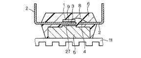
図8は、第1の従来技術における電力用半導体装置の構造を模式的に示す断面図である。図8のように、第1の従来技術における電力用半導体装置は、パワー素子1,金属薄板より成形されているリードフレーム2,放熱用ヒートシンクとして機能する金属ブロック5及び樹脂パッケージ6を備えている。
【0003】
リードフレーム2は、ダイパッド部3とインナーリード部4とを有しており、パワー素子1はダイパッド部3に半田9で接合されている。また、パワー素子1に形成されている電極(図示せず)は、リードフレーム2のインナーリード部4にアルミワイヤ8によって接続されている。金属ブロック5は、その略中央部に凸部を有しており、その凸部がリードフレーム2のパワー素子1とは反対側の面と所定距離を成して、パワー素子1と対向するように配置されている。そして、樹脂パッケージ6は、金属ブロック5のリードフレーム2とは反対側の面を露出させつつ、パワー素子1,リードフレーム2及び金属ブロック5を封止している。そして、金属ブロック5の露出部分に外部放熱器11が取り付けられている。ここで、金属ブロック5の凸部とリードフレーム2との間に形成されている樹脂パッケージ6を樹脂絶縁層27と呼ぶ。
【0004】
なお、ダイパッド部3上には、パワー素子1以外にも、パワー素子1の制御回路を形成するための素子が形成される場合もある。
【0005】
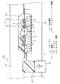
図9は第2の従来技術における電力用半導体装置の構造を模式的に示す断面図であり、図10は、図9中の部分Bを拡大して示す断面図である。かかる構造は、例えば特開平10−93015号公報に開示されている。図9,図10に示されるように、第2の従来技術における電力用半導体装置は、パワー素子1,ダイオード12,熱拡散板15,リードフレーム2,絶縁層37,ヒートシンク25及び樹脂パッケージ6を備えている。
【0006】
パワー素子1は、銅で構成されている熱拡散板15に半田9で接合されている。熱拡散板15のパワー素子1と反対側の面は、銅製リードフレーム2のダイパッド部3に半田9で接合されている。そして、リードフレーム2の熱拡散板15と反対側の面は、絶縁層37によって銅製のヒートシンク25に固着されている。製造工程では、予めリードフレーム2をヒートシンク25に固着し、パワー素子1を接合した熱拡散板15を、そのリードフレーム2のダイパッド部3に接合している。ダイオード12は、パワー素子1ほど発熱しないため、熱拡散板15を介さずに直接リードフレーム2に半田9で接合されている。また、パワー素子1に形成されている電極(図示せず)は、アルミワイヤ8によってリードフレーム2のインナーリード部4に接続されている。そして、樹脂パッケージ6は、ヒートシンク25のリードフレーム2とは反対側の面を露出させつつ、パワー素子1,ダイオード12,リードフレーム2及び熱拡散板15を封止している。
【0007】
【発明が解決しようとする課題】
第1の従来技術における電力半導体装置では、パワー素子1で発生した熱は、リードフレーム2,樹脂絶縁層27,金属ブロック5を通って、外部放熱器11から外部に放出される。金属ブロック5及び外部放熱器11は、アルミニウムあるいは銅材から成り、その熱伝導率はそれぞれ約230W/mK、約390W/mKである。リードフレーム2も銅材などの金属から形成されるため、金属ブロック5及び外部放熱器11と同様の熱伝導率を有している。そして、樹脂絶縁層27を形成する樹脂の熱伝導率は1〜3W/mKである。このように、樹脂絶縁層27は、その熱伝導率がその他の材料の約1/100であって、熱伝導の主たる阻害要因となっている。
【0008】
半導体装置の放熱特性は、熱が通過する材料の厚さや熱伝導性、および熱が材料を通過する面積などで決定される。第1の従来技術における電力半導体装置において、樹脂絶縁層27の厚みを薄くして、熱が通過する熱伝導の悪い部分を抑えることで放熱特性を改善することができる。しかし、樹脂絶縁層27には数千Vの絶縁耐圧が必要であるため、その厚みは0.5mm前後が限界であり、放熱特性の改善にも限界を生じている。
【0009】
また、樹脂絶縁層27を形成する樹脂の充填材として高熱伝導率を持つセラミック粉末、例えば窒化アルミニウム,窒化ケイ素などの粉末を使用し、充填率を高くすることによって、樹脂絶縁層27の熱伝導率を約5W/mKまでに向上させることができる。しかし、樹脂絶縁層27は樹脂パッケージ6の一部であるため、樹脂絶縁層27以外の部分、つまり高熱伝導率を必要としない部分にまで、セラミック粉末を充填した樹脂を使用することになるため、価格の高い樹脂を無駄に使用することになる。その結果、半導体装置の材料コストが増加する。
【0010】
パワー素子1で発生した熱は、まずリードフレーム2を通過して、樹脂絶縁層27を通過する。一般的にリードフレーム2は、加工の問題などで、金属ブロック5などのようにその厚みを厚くすることができないため、金属ブロック5などと比べて熱拡散効果が小さい。そのため、樹脂絶縁層27を熱が通過する面積を十分に広げることが困難であり、このことが放熱特性の改善を制限する原因の一つにもなっていた。
【0011】
第2の従来技術における電力用半導体装置では、パワー素子1と絶縁層37との間に、リードフレーム2と熱拡散板15とが介在しているため、パワー素子1で発生した熱を熱拡散板15でその厚さ方向と垂直な水平方向に拡散し、絶縁層37を熱が通過する面積を広げている。しかし、熱拡散板15はパワー素子1とリードフレーム2との間に位置しており、放熱特性の改善のために水平方向の寸法を大きくすると、パワー素子1とリードフレーム2とを接続するアルミワイヤ8の配線が困難になるという問題があった。また、熱拡散板15を厚くすると、アルミワイヤ8の配線長が長くなり電力損失が増加するという問題もあった。
【0012】
また、熱伝導率を向上するために、絶縁層37のみに、セラミック材を充填した樹脂を使用することがある。つまり、樹脂パッケージ6と絶縁層37とで使用される樹脂が異なる場合がある。このとき、リードフレーム2とヒートシンク25とが接合された後、つまり絶縁層37が硬化した後に、樹脂パッケージ6が形成されると、樹脂パッケージ6と絶縁層37との界面で剥離が起こりやすく、リードフレーム2とヒートシンク25との間の絶縁耐圧が低下するという問題があった。
【0013】
そこで、本発明は上述のような問題を解決するためになされたものであり、放熱特性と絶縁耐圧とのいずれも良好な半導体装置およびその製造方法を提供することを目的とする。
【0014】
【課題を解決するための手段】
この発明のうち請求項1に記載の半導体装置は、半導体素子と、前記半導体素子を搭載する第1の面と、前記第1の面とは反対側の第2の面とを有するリードフレームと、前記リードフレームの前記第2の面に設けられた金属ブロックと、前記リードフレームとは反対側で前記金属ブロックに設けられた絶縁層と、前記リードフレームの前記第2の面と前記金属ブロックとの間に介在し、前記絶縁層よりも熱伝導が良好な接合材とを備え、前記半導体素子は、複数備えられ、前記金属ブロックは、前記半導体素子間の絶縁単位ごとに分離し、かつ少なくとも一つの前記半導体素子に対応して設けられるものである。
【0015】
また、この発明のうち請求項2に記載の半導体装置は、半導体素子と、前記半導体素子を搭載する第1の面と、前記第1の面とは反対側の第2の面とを有するリードフレームと、前記リードフレームの前記第2の面に設けられた金属ブロックと、前記リードフレームとは反対側で前記金属ブロックに設けられた絶縁層と、前記リードフレームの前記第2の面と前記金属ブロックとの間に介在し、前記絶縁層よりも熱伝導が良好な接合材と、前記絶縁層を露出させつつ、前記半導体素子,前記リードフレーム及び前記金属ブロックを封止する樹脂パッケージとを備え、前記絶縁層は、前記樹脂パッケージよりも熱伝導が良好なものである。
【0016】
また、この発明のうち請求項3に記載の半導体装置は、請求項2に記載の半導体装置であって、前記絶縁層は、前記樹脂パッケージと同系の基剤と、セラミック粉末とを含むものである。
【0017】
また、この発明のうち請求項4に記載の半導体装置は、請求項1乃至請求項3のいずれか一つに記載の半導体装置であって、前記金属ブロックは、前記接合材よりも広い面を前記接合材と反対側に有するものである。
【0018】
また、この発明のうち請求項5に記載の半導体装置は、請求項1乃至請求項4のいずれか一つに記載の半導体装置であって、前記金属ブロックの前記リードフレーム側の主面は第1の面及び第2の面を含み、前記第1の面は、前記第2の面よりも前記リードフレーム側に位置しており、前記接合材は、前記リードフレームと前記金属ブロックの前記第1の面との間に介在するものである。
【0019】
また、この発明のうち請求項6に記載の半導体装置は、請求項1乃至請求項5のいずれか一つに記載の半導体装置であって、前記リードフレームは第1の部分と第2の部分からなり、前記第2の部分は前記金属ブロックとの間に絶縁空間を形成するものである。
【0020】
また、この発明のうち請求項7に記載の半導体装置の製造方法は、(a)半導体素子を準備する工程と、(b)第1の樹脂を半硬化で準備する工程と、(c)第1の面と前記第1の面とは反対側に第2の面とを有するリードフレーム及び金属ブロックを準備する工程と、(d)前記工程(a)〜(c)の後に、前記リードフレームの前記第1の面に前記半導体素子を搭載する工程と、(e)前記工程(a)〜(c)の後に、前記リードフレームの前記第2の面に、前記第1の樹脂よりも熱伝導が良好な接合材を介在して金属ブロックを設ける工程と、(f)前記工程(a)〜(c)の後に、前記リードフレームとは反対側で前記金属ブロックに前記第1の樹脂を設ける工程と、(g)前記工程(d),(e),(f)の後に、前記第1の樹脂を露出させつつ、前記半導体素子、前記第1の樹脂の一部、前記リードフレーム及び前記金属ブロックを、第2の樹脂で覆う工程と、(h)前記工程(g)の後に、前記第1の樹脂と前記第2の樹脂とを同時に硬化させる工程とを備えるものである。
【0021】
また、この発明のうち請求項8に記載の半導体装置の製造方法は、請求項7に記載の半導体装置の製造方法であって、前記第1の樹脂は、前記第2の樹脂と同系の基剤と、セラミック粉末とを含むものである。
【0025】
【発明の実施の形態】
実施の形態1.
図1は、本実施の形態1に係る半導体装置の構造を模式的に示す断面図である。図1のように、本実施の形態1に係る半導体装置は、パワー素子1,リードフレーム2a,2b,金属ブロック5及び樹脂パッケージ6を備えている。
【0026】
リードフレーム2a,2bは、熱伝導性の良好な金属、例えば銅合金の薄板から成形されている。リードフレーム2aはダイパッド部3とインナーリード部4とを有しており、リードフレーム2bはインナーリード部4を有している。パワー素子1は両面に電極(図示せず)を有しており、その一方の面の電極がリードフレーム2aと接するように、リードフレーム2aのダイパッド部3に搭載され、半田9でダイパッド部3と接合されている。パワー素子1の他方の面の電極は、リードフレーム2bのインナーリード部4とアルミワイヤ8によって接続されている。リードフレーム2a,2bは分離されており、パワー素子1の両面に形成されている電極間は絶縁されている。
【0027】
金属ブロック5は、例えばアルミニウムや銅などの材料から形成されており、パワー素子1とは反対側の面でリードフレーム2aと接合材10で接合されている。具体的には、金属ブロック5の一方の主面には、接合面50と非接合面51とを有しており、接合面50及び非接合面51がリードフレーム2aと対向するように配置されている。接合面50は、非接合面51よりもパワー素子1側に位置しており、パワー素子1と対向するようにリードフレーム2aに接合材10で接合されている。言い換えれば、金属ブロック5はその表面に凸部を有しており、その凸部がパワー素子1と対向するようにリードフレーム2aに接合されている。そして、金属ブロック5のリードフレーム2aと反対側の面は、リードフレーム2aとのパワー素子1の接合面よりも広くなっている。また、非接合面51は、リードフレーム2bとの間で絶縁空間60を形成している。
【0028】
樹脂パッケージ6は、例えばエポキシ系樹脂が使用されており、リードフレーム2a,2bと反対側の面で金属ブロック5に絶縁層7を形成しつつ、パワー素子1,リードフレーム2a,2b及び金属ブロック5を封止している。そして、外部放熱器11が、金属ブロック5とは反対側の面で絶縁層7に取り付けられている。
【0029】
上述の構造を備える本実施の形態1に係る半導体装置において、パワー素子1で発生した熱は、半田9,リードフレーム2a,接合材10,金属ブロック5,絶縁層7を通って、外部放熱器11から外部に放出される。接合材10は、リードフレーム2aと金属ブロック5との電気的絶縁性を確保する必要がないため、絶縁耐圧を考慮することなく、その材料を選択することができる。具体的には、外部放熱器11に別の半導体装置が取り付けられた場合、半導体装置間の絶縁は、絶縁層7によって維持されるため、接合材10は絶縁耐圧を考慮する必要はない。そのため、接合材10は、絶縁層7よりも熱伝導の良好な材料、例えば半田などを使用することができる。その結果、パワー素子1で発生した熱は、リードフレーム2aから金属ブロック5へと良好に伝導される。
【0030】
また、接合材10として樹脂接着剤を使用した場合であっても、接合材10の厚みを、上述の第1の従来技術における樹脂絶縁層27よりも薄くできる。具体的には、接合材10の厚みを10〜40μmに設定することができ、従来の樹脂絶縁層27の厚みの約1/10倍に低減することができる。また、例えば金属粉を充填材として混入した接着剤、つまり高熱伝導率の接着材を使用することができる。これらの結果、樹脂接着剤で構成された接合材10は、従来の樹脂絶縁層27よりも、その熱伝導率を5〜10倍(5〜20W/mK)に向上することができる。つまり、接合材10として樹脂接着材を使用した場合であっても、パワー素子1で発生した熱を良好に金属ブロック5まで伝導することができる。
【0031】
次に、熱伝導の主たる阻害要因となる絶縁層7を通過する熱について詳細に説明する。図2は、パワー素子1で発生した熱が伝導する様子を示した図であって、図2(a)は、上述の第1の従来技術における電力用半導体装置の熱伝導の様子を示しており、図2(b)は、本実施の形態1に係る半導体装置の熱伝導の様子を示している。図2(a)の熱拡散方向30で示すように、第1の従来技術では、パワー素子1で発生した熱はリードフレーム2で若干水平方向に拡散されるが、リードフレーム2の厚みが薄いため、十分な拡散が行われない。そのため、第1の従来技術において熱伝導の主たる阻害要因であった樹脂絶縁層27を熱が通過する面積32は、ほぼパワー素子1の面積と同じである。一方、図2(b)の熱の拡散方向31で示すように、本実施の形態1では、パワー素子1で発生した熱はリードフレーム2aで若干水平方向に拡散され、さらに十分厚みを持つ金属ブロック5で拡散される。そのため、絶縁層7を熱が通過する面積33は、パワー素子1の面積よりも十分大きい。つまり、本実施の形態1における熱の主たる阻害要因は、第1の従来技術におけるそれよりも小さい。
【0032】
このように、本実施の形態1に係る半導体装置によれば、放熱特性が改善される。
【0033】
また、金属ブロック5は、リードフレーム2bとの間に絶縁空間60を形成しているため、パワー素子1のそれぞれの面の電極同士を絶縁しつつ金属ブロック5の寸法を半導体装置の外形近くまで広げることが可能となり、その結果、放熱特性を向上することができる。
【0034】
また、第2の従来技術では、金属ブロック5の寸法がアルミワイヤ8配線に影響を与えていたが、金属ブロック5はパワー素子1とは反対側でリードフレーム2aに接合されているため、アルミワイヤ8配線への影響を与えることなく、その寸法を決定することできる。
【0035】
また、本実施の形態1では、従来に無い新しい半導体装置の構造を提案しているが、リードフレーム2aと金属ブロック5との接合を樹脂パッケージ6の形成工程の直前に行うことにより、アルミワイヤ8配線までは従来と同じ工程及び装置で製造が可能であるため、新規の設備投資などを抑えることができる。
【0036】
実施の形態2.
図3は本実施の形態2に係る半導体装置の回路図である。図3のように、本実施の形態2に係る半導体装置は、例えば三相インバータ回路で構成されている。具体的には、パワー素子1はIGBT1aと、IGBT1aに逆並列接続されたダイオード1bとを備え、そのパワー素子1同士が直列接続されている。これをアームと呼ぶ。そして、本実施の形態2に係る半導体装置は、並列接続された3つのアームを備えている。
【0037】
出力端子U,V,Wは例えば交流モータなどに接続され、入力端子P,Nは例えば直流電源が直接接続されたり、また商用電源から直流電圧を作る順変換回路の出力が接続されたりする。そして、制御端子GUP,GUN,GVP,GVN,GWP,GWNを制御することによって各IGBTをオン/オフし、交流モータの回転動作を制御する。
【0038】
図4は、本実施の形態2に係る半導体装置の構造を模式的に示す平面図であって、図3の回路図で示された半導体装置の平面図である。そして、図5は、図4中の矢視A−Aにおける断面図であって、樹脂パッケージを形成した後の断面図である。
【0039】
図4及び図5より、本実施の形態2に係る半導体装置は、パワー素子1,リードフレーム2,金属ブロック5,絶縁層17及び樹脂パッケージ6を備えている。図4では、構造を容易に把握できるように樹脂パッケージ6を省略し、これが形成される領域16を示している。
【0040】
本実施の形態2に係る半導体装置は、上述の実施の形態1に係る半導体装置においてパワー素子1を複数備えたものであって、絶縁層17が樹脂パッケージ6と異なる樹脂から構成されているものである。リードフレーム2及び金属ブロック5は、パワー素子1間で絶縁されている単位(絶縁単位)ごとに設けられており、各リードフレーム2のダイパッド部3にパワー素子1が搭載されている。そして、パワー素子1に形成されている電極(図示せず)は、リードフレーム2のインナーリード部4とアルミワイヤ8によって接続されている。各リードフレーム2はタイバー80で接続されているが、このタイバー80は樹脂パッケージ6の形成後に切断され、各リードフレーム2は分離される。
【0041】
金属ブロック5は各リードフレームごとに設けられ、その表面に有する凸部がパワー素子1と対向するようにリードフレーム2に接合されている。
【0042】
絶縁層17は、リードフレーム2と反対側の面で金属ブロック5に形成されており、各金属ブロック5にまたがって形成されている。言い換えれば、一枚の絶縁層17の上に、各金属ブロック5が搭載されている。絶縁層17は、高熱伝導材料、例えばセラミック粉末を充填材として混入した樹脂で形成されている。セラミック粉末には、例えばシリカ,特に結晶性シリカ,アルミナ,窒化アルミニウム,窒化ケイ素,窒化ボロンなどがある。そして、樹脂パッケージ6は、絶縁層17を露出させつつ、パワー素子1,リードフレーム2及び金属ブロック5を封止している。絶縁層17の金属ブロック5と反対側、つまり露出している部分には、外部放熱器が取り付けられることがあるが、図5では記載を省略している。ここで図4において、P側のパワー素子1に対応する金属ブロック5は、N側の金属ブロック5のように各パワー素子1ごとに分離されても良い。つまり、金属ブロック5はパワー素子1間の絶縁単位ごとに設けられ、その絶縁単位の中では少なくとも一つのパワー素子1に対応した金属ブロック5が複数設けられても良い。
【0043】
次に、樹脂パッケージ6の形成方法について説明する。図6は、本実施の形態2に係る半導体装置における樹脂パッケージ6の形成方法を示す図であって、例えばトランスファーモールドによって樹脂パッケージ6は形成される。トランスファーモールド装置100は、プランジャ20と金型21,22とを備えている。金型21と金型22とで形成されるキャビティ23内には、パワー素子1及び金属ブロック5が接合されたリードフレーム2が準備されている。そして、キャビティ底面24と金属ブロック5との間に絶縁層17を配置する。例えば樹脂パッケージ6にエポキシ系樹脂が使用されている場合、同じエポキシ系の樹脂基剤(基剤とは、主剤と硬化剤とを含めたものである)に充填剤としてセラミック粉末を混入し、混練工程後の半硬化状、いわゆる「Bステージ」段階の樹脂が、絶縁層17としてここでは準備されている。そして、タブレット状で準備された封止樹脂26をプランジャ20によって加圧することによって、溶融した封止樹脂26がキャビティ20内に充填される。その後、半硬化状の絶縁層17と封止樹脂26とを同時に硬化・成形することによって、樹脂パッケージ6が形成される。
【0044】
このように、本実施の形態2に係る半導体装置によれば、金属ブロック5は、分離されたリードフレーム2ごとに設けられるため、パワー素子1間の絶縁を維持することができる。
【0045】
また、絶縁層17は、樹脂パッケージ6の一部ではなく別途に設けらているため、放熱特性に影響を与える絶縁層17だけに、高熱伝導の樹脂を使用することができる。その結果、材料コストを低減することができる。
【0046】
また、絶縁層17と樹脂パッケージ6とを同時に硬化・成形するため、異なる樹脂の界面に生じる剥離を減少することができる。その結果、絶縁耐圧が向上する。
【0047】
また、上述の実施の形態1に係る半導体装置では、樹脂パッケージ6に流動性が乏しい材料を使用した場合、絶縁層7の厚みが薄いため、絶縁層7にボイドが発生しやすい。本実施の形態2では、絶縁層17を金属ブロック5の表面に配置したあとに樹脂パッケージ6を形成するため、絶縁層17でのボイドの発生を低減することができる。その結果絶縁耐圧が向上する。また、絶縁層17の厚みが安定するため放熱特性のばらつきを抑えることができる。
【0048】
なお、絶縁層17を金属ブロック5の表面に形成し硬化させた後に、樹脂パッケージ6を形成した半導体装置、あるいは金属ブロック5の表面を露出させつつ、樹脂パッケ−ジを形成し、その後に絶縁層17を形成した半導体装置であっても、絶縁耐圧は低下するが、それ以外の上述の効果は得ることができる。
【0049】
実施の形態3.
図7は、本実施の形態3に係る半導体装置の構造を模式的に示す断面図である。本実施の形態3に係る半導体装置は、上述の実施の形態1に係る半導体装置において、基本的にはリードフレーム2a,2b及び金属ブロック5の形状を変形したものである。
【0050】
パワー素子1は複数の電極(図示せず)を有しており、リードフレーム2a,2bはその電極間を絶縁するために分離されている。そして、パワー素子1は、リードフレーム2aのダイパッド部3に搭載されており、パワー素子1のある電極は、リードフレーム2aのインナーリード部4にアルミワイヤ8で接続されている。また、パワー素子1の別の電極は、パワー素子1が搭載されていないリードフレーム2bのインナーリード部4にアルミワイヤ8で接続されている。結果、パワー素子1のこれらの電極間は絶縁されている。
【0051】
また、リードフレーム2aのダイパッド部3において、パワー素子1とは反対側の面には、金属ブロック5との接合面52を有している。そして、リードフレーム2aのインナーリード部4において、アルミワイヤ8と接続されている面と反対側の面には、接合面52よりもパワー素子1側に位置し、金属ブロック5との間で絶縁空間61を形成している非接合面53を有している。言い換えれば、リードフレーム2aは、そのダイパッド部3が金属ブロック5側に沈められた形状をしており、その沈められた部分と金属ブロック5とが接合材10で接合されている。その他の構造については、上述の実施の形態1に係る半導体装置と同様であるため、ここでは説明を省略する。
【0052】
このように、本実施の形態3に係る半導体装置によれば、リードフレーム2a,2bは、そのダイパッド部3以外では、金属ブロック5との間に絶縁空間61を形成しているため、金属ブロック5の寸法を半導体装置の外形近くまで広げることが可能となり、その結果、放熱特性を向上することができる。
【0053】
また、上述の実施の形態1,2の半導体装置では、金属ブロック5に凸部を有しているため、リードフレーム2,2a,2bとの接合の際に、金属ブロック5の表裏,前後を確認する工程が必要であった。本実施の形態3では、リードフレーム2a,2bの形状を工夫し絶縁空間61を維持しているため、直方体の金属ブロック5を使用することができる。そのため、リードフレーム2との接合時に、金属ブロック5の接合方向を揃える工程が不要になる。その結果、半導体装置の生産性を向上することができる。
【0054】
【発明の効果】
この発明のうち請求項1に係る半導体装置によれば、発熱源である半導体素子から近い位置にある接合材において熱伝導を良好にするため、金属ブロックでの放熱が良好となる。また、絶縁層が金属ブロックに設けられているので、これに絶縁耐圧を担わせることができる。そのため、接合材は絶縁耐圧を考慮することなく熱伝導の観点からその材料を選択することができる。また、金属ブロックが半導体素子の絶縁単位ごとに分離されているため、半導体素子間の絶縁を維持しつつ複数の半導体素子を一つの半導体装置に備えることができる。
【0055】
また、この発明のうち請求項2乃至請求項3に係る半導体装置によれば、発熱源である半導体素子から近い位置にある接合材において熱伝導を良好にするため、金属ブロックでの放熱が良好となる。また、絶縁層が金属ブロックに設けられているので、これに絶縁耐圧を担わせることができる。そのため、接合材は絶縁耐圧を考慮することなく熱伝導の観点からその材料を選択することができる。また、樹脂パッケージよりも熱伝導が良好な絶縁層を備えているため、樹脂パッケージと同一の材料で絶縁層を形成した半導体装置よりも、放熱特性を向上することができる。
【0056】
また、この発明のうち請求項4に係る半導体装置によれば、金属ブロックが接合材よりも広い面を有してるため、半導体素子からの熱を拡散することができる。そのため、熱伝導の主たる阻害要因である絶縁層に、より広い面積の熱を通過させることができる。その結果、放熱特性が改善される。
【0057】
また、この発明のうち請求項5乃至請求項6に係る半導体装置によれば、金属ブロックは、リードフレームとの間に絶縁空間を形成しているため、金属ブロックの寸法を半導体装置の外形近くまで広げることが可能となる。その結果、放熱特性を向上することができる。
【0058】
また、この発明のうち請求項7乃至請求項8に係る半導体装置の製造方法によれば、絶縁層と樹脂パッケージとを同時に硬化するため、異なる樹脂の界面に生じる剥離を減少することができる。その結果、絶縁耐圧が向上する。また、絶縁層と樹脂パッケージとが分離されているため、放熱特性に影響を与える絶縁層だけに、高熱伝導の樹脂を使用することができる。その結果、材料コストを低減することができる。
【図面の簡単な説明】
【図1】 本実施の形態1に係る半導体装置の構造を模式的に示す断面図である。
【図2】 パワー素子1で発生した熱が伝導する様子を示した図である。
【図3】 本実施の形態2に係る半導体装置の回路図である。
【図4】 本実施の形態2に係る半導体装置の構造を模式的に示す平面図である。
【図5】 本実施の形態2に係る半導体装置の構造を模式的に示す断面図である。
【図6】 本実施の形態2における樹脂パッケージ6の形成方法を示す図である。
【図7】 本実施の形態3に係る半導体装置の構造を模式的に示す断面図である。
【図8】 第1の従来技術における電力用半導体装置の構造を模式的に示す断面図である。
【図9】 第2の従来技術における電力用半導体装置の構造を模式的に示す断面図である。
【図10】 第2の従来技術における電力用半導体装置の構造の一部を拡大して示す断面図である。
【符号の説明】
1 パワー素子、2,2a,2b リードフレーム、5 金属ブロック、6 樹脂パッケージ、7,17 絶縁層、10 接合材、50,52 接合面、51,53 非接合面、60,61 絶縁空間。[0001]
BACKGROUND OF THE INVENTION
The present invention relates to a structure of a semiconductor device, and more particularly to a structure of a power semiconductor device used for power control and a manufacturing method thereof.
[0002]
[Prior art]
FIG. 8 is a cross-sectional view schematically showing the structure of the power semiconductor device according to the first prior art. As shown in FIG. 8, the power semiconductor device according to the first prior art includes a
[0003]
The
[0004]
In addition,Die pad sectionIn addition to the
[0005]
FIG. 9 is a cross-sectional view schematically showing the structure of the power semiconductor device according to the second prior art, and FIG. 10 is an enlarged cross-sectional view showing a portion B in FIG. Such a structure is disclosed, for example, in JP-A-10-93015. As shown in FIGS. 9 and 10, the power semiconductor device according to the second prior art includes a
[0006]
The
[0007]
[Problems to be solved by the invention]
In the power semiconductor device according to the first prior art, the heat generated in the
[0008]
The heat dissipation characteristics of a semiconductor device are determined by the thickness and thermal conductivity of a material through which heat passes and the area through which heat passes through the material. In the power semiconductor device according to the first prior art, the heat dissipation characteristics can be improved by reducing the thickness of the
[0009]
In addition, a ceramic powder having a high thermal conductivity, for example, a powder of aluminum nitride, silicon nitride, or the like is used as a resin filler for forming the
[0010]
The heat generated in the
[0011]
In the power semiconductor device according to the second prior art, the
[0012]
Further, in order to improve the thermal conductivity, a resin filled with a ceramic material may be used only for the
[0013]
Accordingly, the present invention has been made to solve the above-described problems, and an object of the present invention is to provide a semiconductor device and a method for manufacturing the semiconductor device that have both excellent heat dissipation characteristics and withstand voltage.
[0014]
[Means for Solving the Problems]
The semiconductor device according to
[0015]
The semiconductor device according to
[0016]
According to a third aspect of the present invention, there is provided a semiconductor device., ContractClaim2The semiconductor device according to
[0017]
A semiconductor device according to a fourth aspect of the present invention is the semiconductor device according to any one of the first to third aspects,The metal block has a surface wider than the bonding material on the side opposite to the bonding material.Is.
[0018]
A semiconductor device according to a fifth aspect of the present invention is the semiconductor device according to any one of the first to fourth aspects,A main surface of the metal block on the lead frame side includes a first surface and a second surface, and the first surface is located closer to the lead frame than the second surface, and the bonding The material is interposed between the lead frame and the first surface of the metal block.Is.
[0019]
According to a sixth aspect of the present invention, there is provided a
[0020]
The semiconductor device according to
[0021]
The semiconductor device according to
[0025]
DETAILED DESCRIPTION OF THE INVENTION
FIG. 1 is a cross-sectional view schematically showing the structure of the semiconductor device according to the first embodiment. As shown in FIG. 1, the semiconductor device according to the first embodiment includes a
[0026]
The lead frames 2a and 2b are formed from a thin plate of a metal having good thermal conductivity, for example, a copper alloy. The
[0027]
The
[0028]
For example, epoxy resin is used for the
[0029]
In the semiconductor device according to the first embodiment having the above-described structure, heat generated in the
[0030]
Even when a resin adhesive is used as the
[0031]
Next, the heat that passes through the insulating
[0032]
Thus, according to the semiconductor device according to the first embodiment, the heat dissipation characteristics are improved.
[0033]
In addition, since the
[0034]
In the second prior art, the dimension of the
[0035]
In the first embodiment, a new structure of a new semiconductor device has been proposed. However, by joining the
[0036]
FIG. 3 is a circuit diagram of the semiconductor device according to the second embodiment. As shown in FIG. 3, the semiconductor device according to the second embodiment is configured by, for example, a three-phase inverter circuit. Specifically, the
[0037]
The output terminals U, V, and W are connected to, for example, an AC motor, and the input terminals P and N are directly connected to, for example, a DC power supply, or connected to the output of a forward conversion circuit that generates a DC voltage from a commercial power supply. Then, each IGBT is turned on / off by controlling the control terminals GUP, GUN, GVP, GVN, GWP, GWN, and the rotational operation of the AC motor is controlled.
[0038]
FIG. 4 is a plan view schematically showing the structure of the semiconductor device according to the second embodiment, and is a plan view of the semiconductor device shown in the circuit diagram of FIG. And FIG. 5 is sectional drawing in the arrow AA in FIG. 4, Comprising: It is sectional drawing after forming the resin package.
[0039]
4 and 5, the semiconductor device according to the second embodiment includes a
[0040]
The semiconductor device according to the second embodiment includes a plurality of
[0041]
The
[0042]
The insulating
[0043]
Next, a method for forming the
[0044]
As described above, according to the semiconductor device according to the second embodiment, the
[0045]
Further, since the insulating
[0046]
In addition, since the insulating
[0047]
Further, in the semiconductor device according to the first embodiment described above, when a material with poor fluidity is used for the
[0048]
After the insulating
[0049]
FIG. 7 is a cross-sectional view schematically showing the structure of the semiconductor device according to the third embodiment. The semiconductor device according to the third embodiment is basically the same as the semiconductor device according to the first embodiment described above, except that the shapes of the lead frames 2a and 2b and the
[0050]
The
[0051]
Further, the
[0052]
As described above, according to the semiconductor device according to the third embodiment, since the lead frames 2a and 2b form the insulating
[0053]
Further, in the semiconductor devices of the first and second embodiments described above, since the
[0054]
【The invention's effect】
Claim of the invention1According to such a semiconductor device, since heat conduction is improved in the bonding material located near the semiconductor element that is a heat generation source, heat dissipation in the metal block is improved.Moreover, since the insulating layer is provided on the metal block, it can bear the withstand voltage. For this reason, the bonding material can be selected from the viewpoint of heat conduction without considering the withstand voltage. In addition, since the metal block is separated for each insulating unit of the semiconductor element, a plurality of semiconductor elements can be provided in one semiconductor device while maintaining insulation between the semiconductor elements.
[0055]
Also,According to the semiconductor device according to the second to third aspects of the present invention, the heat dissipation in the metal block is good because the heat conduction is good in the bonding material located near the semiconductor element as the heat generation source. .Moreover, since the insulating layer is provided on the metal block, it can bear the withstand voltage. For this reason, the bonding material can be selected from the viewpoint of heat conduction without considering the withstand voltage.In addition, since the insulating layer having better heat conduction than the resin package is provided, the heat dissipation characteristics can be improved as compared with the semiconductor device in which the insulating layer is formed of the same material as the resin package.
[0056]
The invention also claims4Since the metal block has a surface wider than the bonding material, the heat from the semiconductor element can be diffused. Therefore, heat of a wider area can be passed through the insulating layer, which is a main impediment to heat conduction. As a result, the heat dissipation characteristics are improved.
[0057]
The invention also claims5 to 6According to the semiconductor device according to the invention, the metal blockSince an insulating space is formed between the lead frame and the lead frame, the size of the metal block can be expanded to near the outer shape of the semiconductor device. As a result, heat dissipation characteristics are improvedbe able to.
[0058]
The invention also claims7 to 8Semiconductor device according toManufacturing methodAccording toSince the insulating layer and the resin package are cured at the same time, peeling occurring at the interface between different resins can be reduced. As a result, the withstand voltage is improved. In addition, since the insulating layer and the resin package are separated from each other, a high thermal conductive resin can be used only for the insulating layer that affects the heat dissipation characteristics. As a result, material costs are reducedcan do.
[Brief description of the drawings]
FIG. 1 is a cross-sectional view schematically showing the structure of a semiconductor device according to a first embodiment.
FIG. 2 is a diagram showing how heat generated in a
FIG. 3 is a circuit diagram of a semiconductor device according to a second embodiment.
FIG. 4 is a plan view schematically showing the structure of a semiconductor device according to a second embodiment.
FIG. 5 is a cross-sectional view schematically showing the structure of a semiconductor device according to a second embodiment.
FIG. 6 is a diagram showing a method for forming a
FIG. 7 is a cross-sectional view schematically showing the structure of a semiconductor device according to a third embodiment.
FIG. 8 is a cross-sectional view schematically showing a structure of a power semiconductor device in the first prior art.
FIG. 9 is a cross-sectional view schematically showing the structure of a power semiconductor device according to a second prior art.
FIG. 10 is an enlarged cross-sectional view showing a part of the structure of a power semiconductor device according to a second prior art.
[Explanation of symbols]
1 Power element, 2, 2a, 2b Lead frame, 5 Metal block, 6 Resin package, 7, 17 Insulating layer, 10 Bonding material, 50, 52 Bonding surface, 51, 53 Non-bonding surface, 60, 61 Insulating space.
Claims (8)
前記半導体素子を搭載する第1の面と、前記第1の面とは反対側の第2の面とを有するリードフレームと、
前記リードフレームの前記第2の面に設けられた金属ブロックと、
前記リードフレームとは反対側で前記金属ブロックに設けられた絶縁層と、
前記リードフレームの前記第2の面と前記金属ブロックとの間に介在し、前記絶縁層よりも熱伝導が良好な接合材と
を備え、
前記半導体素子は、複数備えられ、
前記金属ブロックは、前記半導体素子間の絶縁単位ごとに分離し、かつ少なくとも一つの前記半導体素子に対応して設けられる、半導体装置。 A semiconductor element;
A lead frame having a first surface on which the semiconductor element is mounted and a second surface opposite to the first surface;
A metal block provided on the second surface of the lead frame;
An insulating layer provided on the metal block on the opposite side of the lead frame;
A bonding material interposed between the second surface of the lead frame and the metal block and having better heat conduction than the insulating layer;
With
A plurality of the semiconductor elements are provided,
The said metal block is isolate | separated for every insulation unit between the said semiconductor elements, and is provided corresponding to at least one said semiconductor element .
前記半導体素子を搭載する第1の面と、前記第1の面とは反対側の第2の面とを有するリードフレームと、
前記リードフレームの前記第2の面に設けられた金属ブロックと、
前記リードフレームとは反対側で前記金属ブロックに設けられた絶縁層と、
前記リードフレームの前記第2の面と前記金属ブロックとの間に介在し、前記絶縁層よりも熱伝導が良好な接合材と、
前記絶縁層を露出させつつ、前記半導体素子,前記リードフレーム及び前記金属ブロックを封止する樹脂パッケージと
を備え、
前記絶縁層は、前記樹脂パッケージよりも熱伝導が良好な、半導体装置。 A semiconductor element;
A lead frame having a first surface on which the semiconductor element is mounted and a second surface opposite to the first surface;
A metal block provided on the second surface of the lead frame;
An insulating layer provided on the metal block on the opposite side of the lead frame;
A bonding material that is interposed between the second surface of the lead frame and the metal block and has better thermal conductivity than the insulating layer;
A resin package for sealing the semiconductor element, the lead frame, and the metal block while exposing the insulating layer;
With
The insulating layer is a semiconductor device having better heat conduction than the resin package .
前記第1の面は、前記第2の面よりも前記リードフレーム側に位置しており、
前記接合材は、前記リードフレームと前記金属ブロックの前記第1の面との間に介在する、請求項1乃至請求項4のいずれか一つに記載の半導体装置。 The main surface of the metal block on the lead frame side includes a first surface and a second surface,
The first surface is located closer to the lead frame than the second surface;
5. The semiconductor device according to claim 1 , wherein the bonding material is interposed between the lead frame and the first surface of the metal block .
前記第2の部分は前記金属ブロックとの間に絶縁空間を形成する、請求項1乃至請求項5のいずれか一つに記載の半導体装置。 The lead frame comprises a first part and a second part,
It said second portion forming an insulating space between said metal block, the semiconductor device according to any one of claims 1 to 5.
(b)第1の樹脂を半硬化で準備する工程と、
(c)第1の面と前記第1の面とは反対側に第2の面とを有するリードフレーム及び金属ブロックを準備する工程と、
(d)前記工程(a)〜(c)の後に、前記リードフレームの前記第1の面に前記半導体素子を搭載する工程と、
(e)前記工程(a)〜(c)の後に、前記リードフレームの前記第2の面に、前記第1の樹脂よりも熱伝導が良好な接合材を介在して金属ブロックを設ける工程と、
(f)前記工程(a)〜(c)の後に、前記リードフレームとは反対側で前記金属ブロックに前記第1の樹脂を設ける工程と、
(g)前記工程(d),(e),(f)の後に、前記第1の樹脂の一部を露出させつつ、前記半導体素子、前記第1の樹脂、前記リードフレーム及び前記金属ブロックを、第2の樹脂で覆う工程と、
(h)前記工程(g)の後に、前記第1の樹脂と前記第2の樹脂とを同時に硬化させる工程と
を備える半導体装置の製造方法。 (A) preparing a semiconductor element;
(B) preparing a first resin by semi-curing;
(C) preparing a lead frame and a metal block having a first surface and a second surface opposite to the first surface;
(D) After the steps (a) to (c), mounting the semiconductor element on the first surface of the lead frame;
(E) After the steps (a) to (c), providing a metal block on the second surface of the lead frame with a bonding material having better heat conduction than the first resin interposed therebetween; ,
(F) After the steps (a) to (c), providing the first resin on the metal block on the side opposite to the lead frame;
(G) After the steps (d), (e), and (f), the semiconductor element, the first resin, the lead frame, and the metal block are exposed while exposing a part of the first resin. A step of covering with a second resin;
(H) after the step (g), simultaneously curing the first resin and the second resin;
A method for manufacturing a semiconductor device comprising :
Priority Applications (6)
| Application Number | Priority Date | Filing Date | Title |
|---|---|---|---|
| JP2001033707A JP4286465B2 (en) | 2001-02-09 | 2001-02-09 | Semiconductor device and manufacturing method thereof |
| US09/895,319 US6979909B2 (en) | 2001-02-09 | 2001-07-02 | Semiconductor device and method of manufacturing same |
| KR1020010058940A KR20020066362A (en) | 2001-02-09 | 2001-09-24 | Semiconductor device and method of manufacturing same |
| DE2001149093 DE10149093B4 (en) | 2001-02-09 | 2001-10-05 | Semiconductor device with resin housing |
| KR1020040059215A KR20040080394A (en) | 2001-02-09 | 2004-07-28 | Semiconductor device and method of manufacturing same |
| US11/239,095 US7045907B2 (en) | 2001-02-09 | 2005-09-30 | Semiconductor device and method of manufacturing same |
Applications Claiming Priority (1)
| Application Number | Priority Date | Filing Date | Title |
|---|---|---|---|
| JP2001033707A JP4286465B2 (en) | 2001-02-09 | 2001-02-09 | Semiconductor device and manufacturing method thereof |
Publications (3)
| Publication Number | Publication Date |
|---|---|
| JP2002237562A JP2002237562A (en) | 2002-08-23 |
| JP2002237562A5 JP2002237562A5 (en) | 2006-12-21 |
| JP4286465B2 true JP4286465B2 (en) | 2009-07-01 |
Family
ID=18897415
Family Applications (1)
| Application Number | Title | Priority Date | Filing Date |
|---|---|---|---|
| JP2001033707A Expired - Lifetime JP4286465B2 (en) | 2001-02-09 | 2001-02-09 | Semiconductor device and manufacturing method thereof |
Country Status (4)
| Country | Link |
|---|---|
| US (2) | US6979909B2 (en) |
| JP (1) | JP4286465B2 (en) |
| KR (2) | KR20020066362A (en) |
| DE (1) | DE10149093B4 (en) |
Families Citing this family (92)
| Publication number | Priority date | Publication date | Assignee | Title |
|---|---|---|---|---|
| KR100723454B1 (en) * | 2004-08-21 | 2007-05-30 | 페어차일드코리아반도체 주식회사 | Power module package with high thermal dissipation capability and method for manufacturing the same |
| DE10142971A1 (en) * | 2001-09-01 | 2003-03-27 | Eupec Gmbh & Co Kg | The power semiconductor module |
| JP2003100986A (en) * | 2001-09-26 | 2003-04-04 | Toshiba Corp | Semiconductor device |
| US6677669B2 (en) * | 2002-01-18 | 2004-01-13 | International Rectifier Corporation | Semiconductor package including two semiconductor die disposed within a common clip |
| JP3828036B2 (en) * | 2002-03-28 | 2006-09-27 | 三菱電機株式会社 | Manufacturing method and manufacturing apparatus for resin mold device |
| US8169062B2 (en) * | 2002-07-02 | 2012-05-01 | Alpha And Omega Semiconductor Incorporated | Integrated circuit package for semiconductior devices with improved electric resistance and inductance |
| US7042730B2 (en) * | 2002-07-31 | 2006-05-09 | International Rectifier Corporation | Non-isolated heatsink(s) for power modules |
| KR100902766B1 (en) * | 2002-09-27 | 2009-06-15 | 페어차일드코리아반도체 주식회사 | Discrete package having insulated ceramic heat sink |
| TW582078B (en) * | 2002-11-29 | 2004-04-01 | Chipmos Technologies Bermuda | Packaging process for improving effective die-bonding area |
| US7061025B2 (en) * | 2003-03-10 | 2006-06-13 | Mccolloch Lawrence R | Optoelectronic device packaging assemblies and methods of making the same |
| US6919625B2 (en) * | 2003-07-10 | 2005-07-19 | General Semiconductor, Inc. | Surface mount multichip devices |
| JP2005109100A (en) * | 2003-09-30 | 2005-04-21 | Mitsubishi Electric Corp | Semiconductor device and manufacturing method thereof |
| US7239016B2 (en) * | 2003-10-09 | 2007-07-03 | Denso Corporation | Semiconductor device having heat radiation plate and bonding member |
| JP2005136264A (en) * | 2003-10-31 | 2005-05-26 | Mitsubishi Electric Corp | Power semiconductor device and power semiconductor module |
| US7250672B2 (en) * | 2003-11-13 | 2007-07-31 | International Rectifier Corporation | Dual semiconductor die package with reverse lead form |
| US7149088B2 (en) * | 2004-06-18 | 2006-12-12 | International Rectifier Corporation | Half-bridge power module with insert molded heatsinks |
| US7151309B2 (en) * | 2004-08-27 | 2006-12-19 | Texas Instruments Incorporated | Apparatus for improved power distribution in wirebond semiconductor packages |
| US7812441B2 (en) | 2004-10-21 | 2010-10-12 | Siliconix Technology C.V. | Schottky diode with improved surge capability |
| US7394158B2 (en) * | 2004-10-21 | 2008-07-01 | Siliconix Technology C.V. | Solderable top metal for SiC device |
| JP4784150B2 (en) * | 2004-11-10 | 2011-10-05 | 富士電機株式会社 | Semiconductor device and manufacturing method of semiconductor device |
| US7834376B2 (en) | 2005-03-04 | 2010-11-16 | Siliconix Technology C. V. | Power semiconductor switch |
| US9419092B2 (en) | 2005-03-04 | 2016-08-16 | Vishay-Siliconix | Termination for SiC trench devices |
| JP4644008B2 (en) * | 2005-03-09 | 2011-03-02 | 三菱電機株式会社 | Semiconductor module |
| JP4659534B2 (en) * | 2005-07-04 | 2011-03-30 | 三菱電機株式会社 | Semiconductor device |
| US8368165B2 (en) | 2005-10-20 | 2013-02-05 | Siliconix Technology C. V. | Silicon carbide Schottky diode |
| US7310191B2 (en) | 2006-03-09 | 2007-12-18 | Matsushita Electric Industrial Co., Ltd. | Zoom lens system, imaging device and camera |
| DE102006012781B4 (en) * | 2006-03-17 | 2016-06-16 | Infineon Technologies Ag | Multichip module with improved system carrier and method for its production |
| JP2007299874A (en) * | 2006-04-28 | 2007-11-15 | Matsushita Electric Ind Co Ltd | Thermally conductive substrate, and electrically conductive substrate |
| US20070257343A1 (en) * | 2006-05-05 | 2007-11-08 | Hauenstein Henning M | Die-on-leadframe (dol) with high voltage isolation |
| JP2007312560A (en) * | 2006-05-22 | 2007-11-29 | Toyota Motor Corp | Insulator and rotary electric machine |
| CN101506989B (en) | 2006-07-31 | 2014-02-19 | 威世-硅尼克斯 | Molybdenum barrier metal for sic schottky diode and process of manufacture |
| US7928590B2 (en) * | 2006-08-15 | 2011-04-19 | Qimonda Ag | Integrated circuit package with a heat dissipation device |
| US20080122896A1 (en) * | 2006-11-03 | 2008-05-29 | Stephenson Iii Stanley W | Inkjet printhead with backside power return conductor |
| KR101489325B1 (en) * | 2007-03-12 | 2015-02-06 | 페어차일드코리아반도체 주식회사 | Power module with stacked flip-chip and method of fabricating the same power module |
| US8077475B2 (en) * | 2007-09-27 | 2011-12-13 | Infineon Technologies Ag | Electronic device |
| JP5415823B2 (en) * | 2008-05-16 | 2014-02-12 | 株式会社デンソー | Electronic circuit device and manufacturing method thereof |
| JP5067267B2 (en) * | 2008-06-05 | 2012-11-07 | 三菱電機株式会社 | Resin-sealed semiconductor device and manufacturing method thereof |
| JP5056620B2 (en) * | 2008-06-30 | 2012-10-24 | 新神戸電機株式会社 | Wiring board |
| US8664038B2 (en) * | 2008-12-04 | 2014-03-04 | Stats Chippac Ltd. | Integrated circuit packaging system with stacked paddle and method of manufacture thereof |
| JP2010182911A (en) * | 2009-02-06 | 2010-08-19 | Renesas Electronics Corp | Manufacturing method of semiconductor device and wire bonder |
| DE102009045063C5 (en) | 2009-09-28 | 2017-06-01 | Infineon Technologies Ag | Power semiconductor module with molded-on heat sink, power semiconductor module system and method for producing a power semiconductor module |
| DE102009046172A1 (en) * | 2009-10-29 | 2011-05-05 | Robert Bosch Gmbh | Metallic cooling element i.e. metal plate, for use in circuit housing of printed circuit board, has outer side whose portion is covered with thin layer formed from plastic material, where outer side of layer provides radiation surface |
| JP4947135B2 (en) * | 2009-12-04 | 2012-06-06 | 株式会社デンソー | Semiconductor package and manufacturing method thereof |
| DE102010001565A1 (en) * | 2010-02-04 | 2011-08-04 | Robert Bosch GmbH, 70469 | Power module with a circuit arrangement, electrical / electronic circuit arrangement, method for producing a power module |
| JP4717148B1 (en) * | 2010-05-28 | 2011-07-06 | 株式会社スズデン | Lighting apparatus and method of manufacturing the lighting apparatus |
| JP5257817B2 (en) | 2010-06-15 | 2013-08-07 | 三菱電機株式会社 | Semiconductor device |
| CN102340233B (en) * | 2010-07-15 | 2014-05-07 | 台达电子工业股份有限公司 | Power module |
| US9659845B2 (en) | 2010-12-13 | 2017-05-23 | Infineon Technologies Americas Corp. | Power quad flat no-lead (PQFN) package in a single shunt inverter circuit |
| US9620954B2 (en) | 2010-12-13 | 2017-04-11 | Infineon Technologies Americas Corp. | Semiconductor package having an over-temperature protection circuit utilizing multiple temperature threshold values |
| US9524928B2 (en) | 2010-12-13 | 2016-12-20 | Infineon Technologies Americas Corp. | Power quad flat no-lead (PQFN) package having control and driver circuits |
| US9324646B2 (en) | 2010-12-13 | 2016-04-26 | Infineon Technologies America Corp. | Open source power quad flat no-lead (PQFN) package |
| US9711437B2 (en) | 2010-12-13 | 2017-07-18 | Infineon Technologies Americas Corp. | Semiconductor package having multi-phase power inverter with internal temperature sensor |
| US9449957B2 (en) | 2010-12-13 | 2016-09-20 | Infineon Technologies Americas Corp. | Control and driver circuits on a power quad flat no-lead (PQFN) leadframe |
| US9362215B2 (en) * | 2010-12-13 | 2016-06-07 | Infineon Technologies Americas Corp. | Power quad flat no-lead (PQFN) semiconductor package with leadframe islands for multi-phase power inverter |
| US9355995B2 (en) | 2010-12-13 | 2016-05-31 | Infineon Technologies Americas Corp. | Semiconductor packages utilizing leadframe panels with grooves in connecting bars |
| US8587101B2 (en) | 2010-12-13 | 2013-11-19 | International Rectifier Corporation | Multi-chip module (MCM) power quad flat no-lead (PQFN) semiconductor package utilizing a leadframe for electrical interconnections |
| US9443795B2 (en) | 2010-12-13 | 2016-09-13 | Infineon Technologies Americas Corp. | Power quad flat no-lead (PQFN) package having bootstrap diodes on a common integrated circuit (IC) |
| CN103250243B (en) * | 2010-12-16 | 2016-04-27 | 三菱电机株式会社 | Semiconductor device |
| JP5714916B2 (en) * | 2011-01-12 | 2015-05-07 | ルネサスエレクトロニクス株式会社 | Semiconductor device and manufacturing method thereof |
| JP5936310B2 (en) | 2011-03-17 | 2016-06-22 | 三菱電機株式会社 | Power semiconductor module and its mounting structure |
| JP5602095B2 (en) * | 2011-06-09 | 2014-10-08 | 三菱電機株式会社 | Semiconductor device |
| JP2013070026A (en) | 2011-09-08 | 2013-04-18 | Rohm Co Ltd | Semiconductor device, manufacturing method of semiconductor device, mounting structure of semiconductor device, and power semiconductor device |
| JP5940799B2 (en) | 2011-11-22 | 2016-06-29 | 新光電気工業株式会社 | Electronic component mounting package, electronic component package, and manufacturing method thereof |
| DE102011088218B4 (en) * | 2011-12-12 | 2015-10-15 | Robert Bosch Gmbh | Electronic power module with thermal coupling layers to a cooling element and method of manufacture |
| US8581416B2 (en) * | 2011-12-15 | 2013-11-12 | Semiconductor Components Industries, Llc | Method of forming a semiconductor device and leadframe therefor |
| US8866274B2 (en) | 2012-03-27 | 2014-10-21 | Infineon Technologies Ag | Semiconductor packages and methods of formation thereof |
| US8847385B2 (en) * | 2012-03-27 | 2014-09-30 | Infineon Technologies Ag | Chip arrangement, a method for forming a chip arrangement, a chip package, a method for forming a chip package |
| US8916968B2 (en) | 2012-03-27 | 2014-12-23 | Infineon Technologies Ag | Multichip power semiconductor device |
| JP5919511B2 (en) | 2012-05-16 | 2016-05-18 | パナソニックIpマネジメント株式会社 | Power semiconductor module |
| JP2014056982A (en) * | 2012-09-13 | 2014-03-27 | Mitsubishi Electric Corp | Power semiconductor device and manufacturing method of the same |
| JP2014207430A (en) | 2013-03-21 | 2014-10-30 | ローム株式会社 | Semiconductor device |
| US9324645B2 (en) | 2013-05-23 | 2016-04-26 | Avogy, Inc. | Method and system for co-packaging vertical gallium nitride power devices |
| JP2015006118A (en) * | 2013-06-24 | 2015-01-08 | 株式会社デンソー | Rotary electric machine for vehicle |
| JP2015006116A (en) * | 2013-06-24 | 2015-01-08 | 株式会社デンソー | Rotary electric machine for vehicle |
| US9324809B2 (en) * | 2013-11-18 | 2016-04-26 | Avogy, Inc. | Method and system for interleaved boost converter with co-packaged gallium nitride power devices |
| KR102153041B1 (en) * | 2013-12-04 | 2020-09-07 | 삼성전자주식회사 | Semiconductor device package and method of manufacturing the same |
| DE102014203225A1 (en) * | 2014-02-24 | 2015-01-29 | Siemens Aktiengesellschaft | Arrangement and method for dissipating the heat losses of electrical components high pulse power |
| US20150279793A1 (en) * | 2014-03-27 | 2015-10-01 | Taiwan Semiconductor Manufacturing Company Ltd. | Semiconductor structure and manufacturing method thereof |
| JP6407756B2 (en) * | 2014-03-31 | 2018-10-17 | 株式会社東芝 | Manufacturing method of semiconductor module |
| WO2016084180A1 (en) * | 2014-11-27 | 2016-06-02 | 三菱電機株式会社 | Semiconductor module and semiconductor driving device |
| JP6345583B2 (en) * | 2014-12-03 | 2018-06-20 | ルネサスエレクトロニクス株式会社 | Semiconductor device |
| DE102014118080B4 (en) | 2014-12-08 | 2020-10-15 | Infineon Technologies Ag | Electronic module with a heat spreader and method of making it |
| KR101744536B1 (en) * | 2015-02-09 | 2017-06-08 | 엘지전자 주식회사 | Radiant heat unit and Outdoor unit of air conditioner having the same |
| JP6281506B2 (en) * | 2015-02-24 | 2018-02-21 | トヨタ自動車株式会社 | Semiconductor module |
| JP6522402B2 (en) * | 2015-04-16 | 2019-05-29 | ローム株式会社 | Semiconductor device |
| DE102015110655A1 (en) * | 2015-07-02 | 2017-01-05 | Infineon Technologies Austria Ag | Electronic device and method of manufacturing the same |
| US9859185B2 (en) | 2016-01-28 | 2018-01-02 | Kyocera International, Inc. | Semiconductor packaging structure and package having stress release structure |
| CN108701661A (en) * | 2016-03-07 | 2018-10-23 | 三菱电机株式会社 | The manufacturing method of semiconductor device and semiconductor device |
| JP6673012B2 (en) * | 2016-05-26 | 2020-03-25 | 三菱電機株式会社 | Semiconductor device and manufacturing method thereof |
| JP2019054069A (en) * | 2017-09-14 | 2019-04-04 | 株式会社東芝 | Semiconductor device |
| JP6843731B2 (en) * | 2017-11-22 | 2021-03-17 | 三菱電機株式会社 | Semiconductor device |
| DE102019206523A1 (en) | 2019-05-07 | 2020-11-12 | Zf Friedrichshafen Ag | Power module with housed power semiconductors for controllable electrical power supply to a consumer |
Family Cites Families (17)
| Publication number | Priority date | Publication date | Assignee | Title |
|---|---|---|---|---|
| JPH0671061B2 (en) * | 1989-05-22 | 1994-09-07 | 株式会社東芝 | Resin-sealed semiconductor device |
| US5317194A (en) * | 1989-10-17 | 1994-05-31 | Kabushiki Kaisha Toshiba | Resin-sealed semiconductor device having intermediate silicon thermal dissipation means and embedded heat sink |
| US5293301A (en) * | 1990-11-30 | 1994-03-08 | Shinko Electric Industries Co., Ltd. | Semiconductor device and lead frame used therein |
| US5598034A (en) * | 1992-07-22 | 1997-01-28 | Vlsi Packaging Corporation | Plastic packaging of microelectronic circuit devices |
| JPH06209054A (en) * | 1993-01-08 | 1994-07-26 | Mitsubishi Electric Corp | Semiconductor device |
| JP2564771B2 (en) | 1994-09-05 | 1996-12-18 | 株式会社後藤製作所 | Semiconductor device with heat sink and method of manufacturing the same |
| JP3429921B2 (en) | 1995-10-26 | 2003-07-28 | 三菱電機株式会社 | Semiconductor device |
| JP3516789B2 (en) * | 1995-11-15 | 2004-04-05 | 三菱電機株式会社 | Semiconductor power module |
| JP3345241B2 (en) | 1995-11-30 | 2002-11-18 | 三菱電機株式会社 | Semiconductor device |
| JPH09186269A (en) | 1996-01-05 | 1997-07-15 | Hitachi Ltd | Semiconductor device |
| JPH09260550A (en) | 1996-03-22 | 1997-10-03 | Mitsubishi Electric Corp | Semiconductor device |
| JP3201277B2 (en) | 1996-09-11 | 2001-08-20 | 株式会社日立製作所 | Semiconductor device |
| JPH10135380A (en) | 1996-10-31 | 1998-05-22 | Hitachi Ltd | Semiconductor device |
| US6001672A (en) * | 1997-02-25 | 1999-12-14 | Micron Technology, Inc. | Method for transfer molding encapsulation of a semiconductor die with attached heat sink |
| JPH1117071A (en) | 1997-06-23 | 1999-01-22 | Hitachi Ltd | Semiconductor device |
| JPH11243166A (en) | 1998-02-24 | 1999-09-07 | Fuji Electric Co Ltd | Resin-encapsulate semiconductor device |
| JP3677403B2 (en) * | 1998-12-07 | 2005-08-03 | パイオニア株式会社 | Heat dissipation structure |
-
2001
- 2001-02-09 JP JP2001033707A patent/JP4286465B2/en not_active Expired - Lifetime
- 2001-07-02 US US09/895,319 patent/US6979909B2/en not_active Expired - Lifetime
- 2001-09-24 KR KR1020010058940A patent/KR20020066362A/en not_active Application Discontinuation
- 2001-10-05 DE DE2001149093 patent/DE10149093B4/en not_active Expired - Lifetime
-
2004
- 2004-07-28 KR KR1020040059215A patent/KR20040080394A/en not_active Application Discontinuation
-
2005
- 2005-09-30 US US11/239,095 patent/US7045907B2/en not_active Expired - Lifetime
Also Published As
| Publication number | Publication date |
|---|---|
| DE10149093B4 (en) | 2009-05-07 |
| US7045907B2 (en) | 2006-05-16 |
| KR20020066362A (en) | 2002-08-16 |
| US6979909B2 (en) | 2005-12-27 |
| KR20040080394A (en) | 2004-09-18 |
| JP2002237562A (en) | 2002-08-23 |
| DE10149093A1 (en) | 2002-08-29 |
| US20020109211A1 (en) | 2002-08-15 |
| US20060022331A1 (en) | 2006-02-02 |
Similar Documents
| Publication | Publication Date | Title |
|---|---|---|
| JP4286465B2 (en) | Semiconductor device and manufacturing method thereof | |
| JP5279632B2 (en) | Semiconductor module | |
| JP6824913B2 (en) | Power semiconductor devices and their manufacturing methods | |
| JP6115738B2 (en) | Semiconductor device and manufacturing method thereof | |
| JP2003124437A (en) | Semiconductor device | |
| JP2002246515A (en) | Semiconductor device | |
| US8912644B2 (en) | Semiconductor device and method for manufacturing same | |
| JPWO2016136457A1 (en) | Power module | |
| JP5895220B2 (en) | Manufacturing method of semiconductor device | |
| JPH11204724A (en) | Power module | |
| US11862542B2 (en) | Dual side cooling power module and manufacturing method of the same | |
| CN111095537B (en) | Semiconductor device and power conversion device provided with same | |
| JP2010192591A (en) | Power semiconductor device and method of manufacturing the same | |
| JP4784150B2 (en) | Semiconductor device and manufacturing method of semiconductor device | |
| JP2002329804A (en) | Semiconductor device | |
| JP2002329828A (en) | Semiconductor device | |
| JP7072624B1 (en) | Power semiconductor devices and methods for manufacturing power semiconductor devices | |
| JP2005116963A (en) | Semiconductor device | |
| JP3770164B2 (en) | Semiconductor device and manufacturing method thereof | |
| JP2014107519A (en) | Semiconductor device and manufacturing method of the same | |
| JP7479771B2 (en) | Semiconductor device, manufacturing method thereof, and power conversion device | |
| WO2022208870A1 (en) | Semiconductor device and semiconductor device production method | |
| WO2022259395A1 (en) | Semiconductor manufacturing device and method for manufacturing semiconductor device | |
| WO2022162871A1 (en) | Dual-side cooled power module | |
| JP2023054418A (en) | Power semiconductor device and manufacturing method thereof |
Legal Events
| Date | Code | Title | Description |
|---|---|---|---|
| A521 | Request for written amendment filed |
Free format text: JAPANESE INTERMEDIATE CODE: A523 Effective date: 20061101 |
|
| A621 | Written request for application examination |
Free format text: JAPANESE INTERMEDIATE CODE: A621 Effective date: 20061101 |
|
| A977 | Report on retrieval |
Free format text: JAPANESE INTERMEDIATE CODE: A971007 Effective date: 20081226 |
|
| A131 | Notification of reasons for refusal |
Free format text: JAPANESE INTERMEDIATE CODE: A131 Effective date: 20090106 |
|
| A521 | Request for written amendment filed |
Free format text: JAPANESE INTERMEDIATE CODE: A523 Effective date: 20090227 |
|
| RD04 | Notification of resignation of power of attorney |
Free format text: JAPANESE INTERMEDIATE CODE: A7424 Effective date: 20090227 |
|
| TRDD | Decision of grant or rejection written | ||
| A01 | Written decision to grant a patent or to grant a registration (utility model) |
Free format text: JAPANESE INTERMEDIATE CODE: A01 Effective date: 20090324 |
|
| A01 | Written decision to grant a patent or to grant a registration (utility model) |
Free format text: JAPANESE INTERMEDIATE CODE: A01 |
|
| A61 | First payment of annual fees (during grant procedure) |
Free format text: JAPANESE INTERMEDIATE CODE: A61 Effective date: 20090325 |
|
| FPAY | Renewal fee payment (event date is renewal date of database) |
Free format text: PAYMENT UNTIL: 20120403 Year of fee payment: 3 |
|
| R150 | Certificate of patent or registration of utility model |
Ref document number: 4286465 Country of ref document: JP Free format text: JAPANESE INTERMEDIATE CODE: R150 Free format text: JAPANESE INTERMEDIATE CODE: R150 |
|
| FPAY | Renewal fee payment (event date is renewal date of database) |
Free format text: PAYMENT UNTIL: 20120403 Year of fee payment: 3 |
|
| FPAY | Renewal fee payment (event date is renewal date of database) |
Free format text: PAYMENT UNTIL: 20130403 Year of fee payment: 4 |
|
| FPAY | Renewal fee payment (event date is renewal date of database) |
Free format text: PAYMENT UNTIL: 20130403 Year of fee payment: 4 |
|
| FPAY | Renewal fee payment (event date is renewal date of database) |
Free format text: PAYMENT UNTIL: 20140403 Year of fee payment: 5 |
|
| R250 | Receipt of annual fees |
Free format text: JAPANESE INTERMEDIATE CODE: R250 |
|
| R250 | Receipt of annual fees |
Free format text: JAPANESE INTERMEDIATE CODE: R250 |
|
| R250 | Receipt of annual fees |
Free format text: JAPANESE INTERMEDIATE CODE: R250 |
|
| R250 | Receipt of annual fees |
Free format text: JAPANESE INTERMEDIATE CODE: R250 |
|
| R250 | Receipt of annual fees |
Free format text: JAPANESE INTERMEDIATE CODE: R250 |
|
| EXPY | Cancellation because of completion of term |