JP4269709B2 - Light emitting device and manufacturing method thereof - Google Patents
Light emitting device and manufacturing method thereof Download PDFInfo
- Publication number
- JP4269709B2 JP4269709B2 JP2003040712A JP2003040712A JP4269709B2 JP 4269709 B2 JP4269709 B2 JP 4269709B2 JP 2003040712 A JP2003040712 A JP 2003040712A JP 2003040712 A JP2003040712 A JP 2003040712A JP 4269709 B2 JP4269709 B2 JP 4269709B2
- Authority
- JP
- Japan
- Prior art keywords
- light emitting
- light
- emitting device
- main surface
- emitting element
- Prior art date
- Legal status (The legal status is an assumption and is not a legal conclusion. Google has not performed a legal analysis and makes no representation as to the accuracy of the status listed.)
- Expired - Lifetime
Links
Images


Classifications
-
- H—ELECTRICITY
- H01—ELECTRIC ELEMENTS
- H01L—SEMICONDUCTOR DEVICES NOT COVERED BY CLASS H10
- H01L2224/00—Indexing scheme for arrangements for connecting or disconnecting semiconductor or solid-state bodies and methods related thereto as covered by H01L24/00
- H01L2224/01—Means for bonding being attached to, or being formed on, the surface to be connected, e.g. chip-to-package, die-attach, "first-level" interconnects; Manufacturing methods related thereto
- H01L2224/26—Layer connectors, e.g. plate connectors, solder or adhesive layers; Manufacturing methods related thereto
- H01L2224/31—Structure, shape, material or disposition of the layer connectors after the connecting process
- H01L2224/32—Structure, shape, material or disposition of the layer connectors after the connecting process of an individual layer connector
- H01L2224/321—Disposition
- H01L2224/32151—Disposition the layer connector connecting between a semiconductor or solid-state body and an item not being a semiconductor or solid-state body, e.g. chip-to-substrate, chip-to-passive
- H01L2224/32221—Disposition the layer connector connecting between a semiconductor or solid-state body and an item not being a semiconductor or solid-state body, e.g. chip-to-substrate, chip-to-passive the body and the item being stacked
- H01L2224/32245—Disposition the layer connector connecting between a semiconductor or solid-state body and an item not being a semiconductor or solid-state body, e.g. chip-to-substrate, chip-to-passive the body and the item being stacked the item being metallic
-
- H—ELECTRICITY
- H01—ELECTRIC ELEMENTS
- H01L—SEMICONDUCTOR DEVICES NOT COVERED BY CLASS H10
- H01L2224/00—Indexing scheme for arrangements for connecting or disconnecting semiconductor or solid-state bodies and methods related thereto as covered by H01L24/00
- H01L2224/01—Means for bonding being attached to, or being formed on, the surface to be connected, e.g. chip-to-package, die-attach, "first-level" interconnects; Manufacturing methods related thereto
- H01L2224/42—Wire connectors; Manufacturing methods related thereto
- H01L2224/44—Structure, shape, material or disposition of the wire connectors prior to the connecting process
- H01L2224/45—Structure, shape, material or disposition of the wire connectors prior to the connecting process of an individual wire connector
- H01L2224/45001—Core members of the connector
- H01L2224/45099—Material
- H01L2224/451—Material with a principal constituent of the material being a metal or a metalloid, e.g. boron (B), silicon (Si), germanium (Ge), arsenic (As), antimony (Sb), tellurium (Te) and polonium (Po), and alloys thereof
- H01L2224/45138—Material with a principal constituent of the material being a metal or a metalloid, e.g. boron (B), silicon (Si), germanium (Ge), arsenic (As), antimony (Sb), tellurium (Te) and polonium (Po), and alloys thereof the principal constituent melting at a temperature of greater than or equal to 950°C and less than 1550°C
- H01L2224/45139—Silver (Ag) as principal constituent
-
- H—ELECTRICITY
- H01—ELECTRIC ELEMENTS
- H01L—SEMICONDUCTOR DEVICES NOT COVERED BY CLASS H10
- H01L2224/00—Indexing scheme for arrangements for connecting or disconnecting semiconductor or solid-state bodies and methods related thereto as covered by H01L24/00
- H01L2224/01—Means for bonding being attached to, or being formed on, the surface to be connected, e.g. chip-to-package, die-attach, "first-level" interconnects; Manufacturing methods related thereto
- H01L2224/42—Wire connectors; Manufacturing methods related thereto
- H01L2224/44—Structure, shape, material or disposition of the wire connectors prior to the connecting process
- H01L2224/45—Structure, shape, material or disposition of the wire connectors prior to the connecting process of an individual wire connector
- H01L2224/45001—Core members of the connector
- H01L2224/45099—Material
- H01L2224/451—Material with a principal constituent of the material being a metal or a metalloid, e.g. boron (B), silicon (Si), germanium (Ge), arsenic (As), antimony (Sb), tellurium (Te) and polonium (Po), and alloys thereof
- H01L2224/45138—Material with a principal constituent of the material being a metal or a metalloid, e.g. boron (B), silicon (Si), germanium (Ge), arsenic (As), antimony (Sb), tellurium (Te) and polonium (Po), and alloys thereof the principal constituent melting at a temperature of greater than or equal to 950°C and less than 1550°C
- H01L2224/45144—Gold (Au) as principal constituent
-
- H—ELECTRICITY
- H01—ELECTRIC ELEMENTS
- H01L—SEMICONDUCTOR DEVICES NOT COVERED BY CLASS H10
- H01L2224/00—Indexing scheme for arrangements for connecting or disconnecting semiconductor or solid-state bodies and methods related thereto as covered by H01L24/00
- H01L2224/01—Means for bonding being attached to, or being formed on, the surface to be connected, e.g. chip-to-package, die-attach, "first-level" interconnects; Manufacturing methods related thereto
- H01L2224/42—Wire connectors; Manufacturing methods related thereto
- H01L2224/47—Structure, shape, material or disposition of the wire connectors after the connecting process
- H01L2224/48—Structure, shape, material or disposition of the wire connectors after the connecting process of an individual wire connector
- H01L2224/4805—Shape
- H01L2224/4809—Loop shape
- H01L2224/48091—Arched
-
- H—ELECTRICITY
- H01—ELECTRIC ELEMENTS
- H01L—SEMICONDUCTOR DEVICES NOT COVERED BY CLASS H10
- H01L2224/00—Indexing scheme for arrangements for connecting or disconnecting semiconductor or solid-state bodies and methods related thereto as covered by H01L24/00
- H01L2224/01—Means for bonding being attached to, or being formed on, the surface to be connected, e.g. chip-to-package, die-attach, "first-level" interconnects; Manufacturing methods related thereto
- H01L2224/42—Wire connectors; Manufacturing methods related thereto
- H01L2224/47—Structure, shape, material or disposition of the wire connectors after the connecting process
- H01L2224/48—Structure, shape, material or disposition of the wire connectors after the connecting process of an individual wire connector
- H01L2224/481—Disposition
- H01L2224/48151—Connecting between a semiconductor or solid-state body and an item not being a semiconductor or solid-state body, e.g. chip-to-substrate, chip-to-passive
- H01L2224/48221—Connecting between a semiconductor or solid-state body and an item not being a semiconductor or solid-state body, e.g. chip-to-substrate, chip-to-passive the body and the item being stacked
- H01L2224/48245—Connecting between a semiconductor or solid-state body and an item not being a semiconductor or solid-state body, e.g. chip-to-substrate, chip-to-passive the body and the item being stacked the item being metallic
- H01L2224/48247—Connecting between a semiconductor or solid-state body and an item not being a semiconductor or solid-state body, e.g. chip-to-substrate, chip-to-passive the body and the item being stacked the item being metallic connecting the wire to a bond pad of the item
-
- H—ELECTRICITY
- H01—ELECTRIC ELEMENTS
- H01L—SEMICONDUCTOR DEVICES NOT COVERED BY CLASS H10
- H01L2224/00—Indexing scheme for arrangements for connecting or disconnecting semiconductor or solid-state bodies and methods related thereto as covered by H01L24/00
- H01L2224/01—Means for bonding being attached to, or being formed on, the surface to be connected, e.g. chip-to-package, die-attach, "first-level" interconnects; Manufacturing methods related thereto
- H01L2224/42—Wire connectors; Manufacturing methods related thereto
- H01L2224/47—Structure, shape, material or disposition of the wire connectors after the connecting process
- H01L2224/48—Structure, shape, material or disposition of the wire connectors after the connecting process of an individual wire connector
- H01L2224/484—Connecting portions
- H01L2224/48463—Connecting portions the connecting portion on the bonding area of the semiconductor or solid-state body being a ball bond
- H01L2224/48465—Connecting portions the connecting portion on the bonding area of the semiconductor or solid-state body being a ball bond the other connecting portion not on the bonding area being a wedge bond, i.e. ball-to-wedge, regular stitch
-
- H—ELECTRICITY
- H01—ELECTRIC ELEMENTS
- H01L—SEMICONDUCTOR DEVICES NOT COVERED BY CLASS H10
- H01L2224/00—Indexing scheme for arrangements for connecting or disconnecting semiconductor or solid-state bodies and methods related thereto as covered by H01L24/00
- H01L2224/01—Means for bonding being attached to, or being formed on, the surface to be connected, e.g. chip-to-package, die-attach, "first-level" interconnects; Manufacturing methods related thereto
- H01L2224/42—Wire connectors; Manufacturing methods related thereto
- H01L2224/47—Structure, shape, material or disposition of the wire connectors after the connecting process
- H01L2224/49—Structure, shape, material or disposition of the wire connectors after the connecting process of a plurality of wire connectors
- H01L2224/491—Disposition
- H01L2224/49105—Connecting at different heights
- H01L2224/49107—Connecting at different heights on the semiconductor or solid-state body
-
- H—ELECTRICITY
- H01—ELECTRIC ELEMENTS
- H01L—SEMICONDUCTOR DEVICES NOT COVERED BY CLASS H10
- H01L2224/00—Indexing scheme for arrangements for connecting or disconnecting semiconductor or solid-state bodies and methods related thereto as covered by H01L24/00
- H01L2224/73—Means for bonding being of different types provided for in two or more of groups H01L2224/10, H01L2224/18, H01L2224/26, H01L2224/34, H01L2224/42, H01L2224/50, H01L2224/63, H01L2224/71
- H01L2224/732—Location after the connecting process
- H01L2224/73251—Location after the connecting process on different surfaces
- H01L2224/73265—Layer and wire connectors
-
- H—ELECTRICITY
- H01—ELECTRIC ELEMENTS
- H01L—SEMICONDUCTOR DEVICES NOT COVERED BY CLASS H10
- H01L2224/00—Indexing scheme for arrangements for connecting or disconnecting semiconductor or solid-state bodies and methods related thereto as covered by H01L24/00
- H01L2224/80—Methods for connecting semiconductor or other solid state bodies using means for bonding being attached to, or being formed on, the surface to be connected
- H01L2224/85—Methods for connecting semiconductor or other solid state bodies using means for bonding being attached to, or being formed on, the surface to be connected using a wire connector
- H01L2224/85909—Post-treatment of the connector or wire bonding area
- H01L2224/8592—Applying permanent coating, e.g. protective coating
-
- H—ELECTRICITY
- H01—ELECTRIC ELEMENTS
- H01L—SEMICONDUCTOR DEVICES NOT COVERED BY CLASS H10
- H01L2924/00—Indexing scheme for arrangements or methods for connecting or disconnecting semiconductor or solid-state bodies as covered by H01L24/00
- H01L2924/0001—Technical content checked by a classifier
- H01L2924/00014—Technical content checked by a classifier the subject-matter covered by the group, the symbol of which is combined with the symbol of this group, being disclosed without further technical details
-
- H—ELECTRICITY
- H01—ELECTRIC ELEMENTS
- H01L—SEMICONDUCTOR DEVICES NOT COVERED BY CLASS H10
- H01L2924/00—Indexing scheme for arrangements or methods for connecting or disconnecting semiconductor or solid-state bodies as covered by H01L24/00
- H01L2924/15—Details of package parts other than the semiconductor or other solid state devices to be connected
- H01L2924/181—Encapsulation
Landscapes
- Led Device Packages (AREA)
- Led Devices (AREA)
Description
【0001】
【発明の属する技術分野】
本発明はバックライト光源、ディスプレイ、照明など各種光源や光センサに利用される発光装置に係わり、特に、良好な信頼性と光学特性とを兼ね合わせた発光装置に関するものである。
【0002】
【従来技術】
今日、高輝度、高出力な半導体発光素子や小型且つ高感度な発光装置が開発され種々の分野に利用されている。このような発光装置は、低消費電力、小型、及び軽量などの特徴を生かして、例えば、光プリンターヘッドの光源、液晶バックライト光源、各種メータの光源や各種読み取りセンサーなどに利用されている。
【0003】
このような発光装置の一例として、図23に示す如き発光装置が挙げられる。凹部を有し且つリード電極が挿入されて一体成形されたプラスチック・パッケージ5を用い、前記凹部内底面から露出されたリード電極2上に発光素子としてLEDチップをダイボンドすると共にLEDチップの各電極とパッケージに設けられたリード電極とを金線などにより電気的に接続させる。このようにして凹部内に配置されたLEDチップは硬化後に剛性を有する透光性部材によって封止される。これにより、パッケージ内部に配置されたLEDチップやワイヤなどを、水分、外力など外部環境から保護することができ、極めて高い信頼性を有する発光装置が得られる。
【0004】
しかしながら、このような発光装置は、利用分野の広がりからより厳しい環境条件で使用され始めている。航空機や車載用に利用される発光装置では、例えば外気温により−20℃以下+80℃以上にまで変化する場合もある。また、外気圧、熱衝撃などと同時に振動もある。このような場合、熱応力により各構成部材が膨張や収縮をくり返すことになり、それぞれの構造的一体性が弱くなり、光学特性に悪影響を及ぼす他、信頼性も低下してしまう。また、近紫外領域において高輝度に発光することが可能な発光素子が開発され使用されている現在において、上記領域の光による各部材の劣化を抑制することが重要となっている。
【0005】
そこで近年、光により切断されないシロキサン結合を有する樹脂が注目されている。このような樹脂は、上記領域の波長に対して優れた耐光性を有する他、柔軟性が高く且つ熱に対して高い安定性を有する。
【0006】
しかしながら、柔軟性を有することにより表面も軟質であり機械的強度が弱く、発光装置の外装としては不向きである。また、表面にタック性を有するため、異物が付着するため、発光面としては不向きである。
【0007】
そこで、特開2000−150968号には、放熱性に優れたパッケージを用い、上記金属製基体上に載置された発光素子を、空壁内部に柔軟性を有し且つ耐光性に優れた部材を備えた剛性カバーにて被覆してなる発光装置が記載されている。このように構成された発光装置は、優れた耐熱性、耐光性、および外部からの機械的強度を兼ね備えることが可能となる。
【0008】
【特許文献1】
特開2000−150968号公報
【0009】
【発明が解決しようとする課題】
しかしながら、上記の如く、柔軟性を有する部材を剛性部材にて封止すると、封止する際に柔軟性部材に気泡が混入されやすい傾向にある。特に、気体を通過しない金属やガラス等からなる剛性部材にて密封すると、前記気泡により熱安定性が損なわれた柔軟性部材が熱応力を緩和できなくなり、隣接する剛性部材を破損する場合がある。また、柔軟性部材と剛性部材との界面に気泡が含有された場合、前記気泡が起因してこれらの界面が剥離され空気層が形成され、発光出力の低下や光学特性の変動が生じる。
【0010】
そこで本発明は、上記課題を解決し、高い信頼性を有し安定した光学特性を有する発光装置を提供する。
【0011】
【発明を解決するための手段】
本発明の発光装置は、パッケージに設けられた凹部に配置された発光素子と、その発光素子を被覆する第一の透光性部材と、その第一の透光性部材に載置される第二の透光性部材と、を備える発光装置であって、上記第二の透光性部材は、上記発光素子の方向へ突出された凸形状と、その凸形状の外側に鍔部と、を有しており、上記鍔部は、上記パッケージの凹部内に配置され、上記第一の透光性部材により被覆されていることを特徴とする。
【0012】
発光素子チップを柔軟性部材である第一の透光性部材と剛性部材である第二の透光性部材とを積層させて封止すると、これらの界面から気泡が混入されやすい。気泡が存在する発光装置は、高温下になると気泡の揮発爆発により一体性が損なわれてしまうため、実装基板等に一度に半田付けすることが可能なリフロー実装を施すことができず、量産性が乏しい。これに対して本願発明の発光装置は、剛性部材の形状を特定することにより、上記問題を解決し、リフロー実装をすることが可能な高い信頼性を有しており、Pbフリー実装にも対応することが可能である。
【0013】
上記背面の断面形状は、上記発光素子方向へ突出していれば特に限定されないが、一点にて発光素子と最近接しているようなV字型であると、気泡混入の防止効率が高まり好ましい。
【0014】
さらに、その一点が第二の透光性部材における背面の中央部であると、界面全体において気泡の混入を効率よく防止することができる。また、この背面を曲面とし、このような構成を有する背面にて柔軟性部材に圧力を加えると、上記柔軟性部材の流動速度が高速化されると共に気泡の脱泡効力を高めることができる。これにより、信頼性の高い発光装置を量産性良く形成することができる。また、下方の柔軟性部材との密着性が向上され好ましい。また、背面を凸形状とすると、剛性部材の主面側に柔軟性部材があふれ出ることを抑制することができる。
【0015】
上記剛性部材の下端は、外側へ広がる鍔部を有し、該鍔部の側面及び主面は上記柔軟性部材にて被覆されている。このように鍔部を設けることにより、剛性部材の取り付け作業の容易化される。また、柔軟性部材との密着性が向上され、光学特性に悪影響を及ぼすことなく信頼性を高めることができる。
【0016】
上記パッケージの凹部は、少なくとも第一の主面と、その第一の主面の上方にて外側へ広がる第二の主面と、その第二の主面より上方にて外側へ広がる第三主面とを有し、上記柔軟性部材は、上記第一の主面、上記第二の主面、および上記剛性部材の下端部に渡り連続的に設けられることが好ましい。これにより、別途接着剤を用いることなく各部材の一体性を保つことができ、信頼性に優れた発光装置が得られる。これに対し少量の接着剤等で各部材を接着すると、接着剤等が局所的に熱劣化や光劣化し、これに起因して信頼性が低下してしまうが、上記構成とすることにより、局所的劣化を防止し、発光装置の長寿命化を実現している。
【0017】
上記第二の主面は、上記第一の主面上に離間して設けられた少なくとも3以上の各支持台の主面であり、上記剛性部材の一背面は上記第二の主面と接していることが好ましい。このような構成により、厳しい環境下にて使用され剛性部材と柔軟性部材とに剥離が生じたとしても、剥離箇所を前記支持台付近に制御することができ、光学特性を維持することができる。
【0018】
上記剛性部材は、上記第二の主面の外郭内に少なくとも3以上の接点を有して内接しており、上記第一の主面および上記第二の主面は、それぞれ、上記剛性部材の各接点間外部に露出部を有することが好ましい。このように構成された発光装置は、柔軟性部材上に剛性部材を載置する際に係る圧力を利用し、上記第二の主面により精度良く位置決めされた剛性部材と上記第一の主面の露出部の作用により、柔軟性部材中または柔軟性部材と剛性部材との界面に混入した気泡を外部へ放出し、高い信頼性及び安定した光学特性を有する発光装置を歩留まり良く容易な手法にて得ることができる。上記柔軟性部材の表面は、硬化前の塗布された状態では表面張力により中央部が上方に凸を有する形状となる場合が多く、この凸部を一背面により圧力をかけパッケージ凹部により流動させることにより、柔軟性部材全体において気泡の脱泡作用を施すことができる。また、本発明の発光装置は、上記脱泡作用の際にオーバーフローされる柔軟性部材を利用し上記剛性部材と一体成型化されている。また、剛性部材の主面は、背面と反対側へ突出した曲面を有することが好ましい。このような形状を有する発光面は、凹部の内壁により反射散乱された光を集光し正面方向における輝度を高めることができる。特に、上記の如く凹部方向へ突出した曲面を有する背面は、光が拡散された状態にて剛性部材中へと入射されるので、主面側に背面と反対側へ突出した曲面を設け、光を集光させることが好ましい。
【0019】
更に、上記剛性部材の下端は、外側へ広がる鍔部を有し、該鍔部の側面及び主面は上記柔軟性部材にて被覆され、上記鍔部の背面は、上記第二の主面と平行で且つ対向していることが好ましく、これにより剛性部材と上記第二の主面との位置決め精度が向上され、各発光装置間に光軸のズレを生じることなく信頼性の高い発光装置を量産性良く提供することができる。
【0020】
第二の主面の外郭を、上記剛性部材の外郭より多くの角を有する多角形とすると、高密度実装することが可能な小型発光装置が得られる。
【0021】
剛性部材の外郭が上記接点においてRを帯びていると、第二の主面へ柔軟性部材をオーバーフローさせる速度が高速化され、剛性部材を迅速に固着することができる。これにより、柔軟性部材へ係る応力が強まり、脱泡作用が向上し信頼性が高まる。さらに、上記第二の主面および剛性部材下端部にかけて設けられる柔軟性部材は、なだらかで平坦な主面となり、好ましい外観が得られる。
【0022】
上記第一の主面において、上記露出部は、中央領域より外側へ突出した凸部であることが好ましい。このような形状とすることにより、柔軟性部材を良好に第二の主面及び剛性部材下端部へ効率よく流動することができる。また、柔軟性部材が上記凸部壁面と衝突することにより、柔軟性部材の脱泡作用が向上される。上記凸部は、上記第二の主面の角と対向していると、上記第二の主面の露出部上に均等な膜厚を有する柔軟性部材を形成することができ、構造的一体性を強化することができる。また、上記凸部の先端はRが帯びていると、更に効果が増大する。
【0023】
パッケージが、側面より一対のリード電極が挿入され成形樹脂にて一体成形されたものであるとき、上記リード電極のインナー部は、上記第一の主面において該第一の主面の外郭に沿って露出されていることが好ましい。リード電極の表面は金属であるため、柔軟性部材の流動性が優れていると考えられる。本発明は、パッケージの各側壁にて柔軟性部材を衝突反動させ上方へ流動させる構成とすることにより、高い信頼性を有しているが、リード電極を前記衝突反動が行われる側壁に沿って設けると、柔軟性部材の衝突反動速度が加速され、気泡の脱泡作用の効果が強められる。
【0024】
リード電極のインナー部は、上記第一の主面の露出部から内側の二方向へ分離して設けられていることが好ましく、これにより上記効果を更に向上させることができる。また、一体成形されたリード電極の抜けが防止される。また、保護素子のような他の素子を載置する必要がある場合、それぞれの分離枝リードの間に載置することにより、電気的に接続させると、発光観測面に関与しない位置に前記素子を載置することができ好ましい。
【0025】
リード電極のインナー部は、背面の一部がパッケージ背面側から貫通した微小孔より露出していることが好ましい。これにより、ワイヤボンディングされる際や剛性部材を載置する際に受けるリード電極の応力を和らげることができる。これにより、リード電極と各部材との構造的一体化を強化することができる。
【0026】
パッケージは、背面が実装面となる金属基体を有し、該金属基体の主面は上記凹部の底面から露出され、金属基体に発光素子が載置されていることが好ましい。これにより、発光素子から生じる熱を良好に実装基板へと放熱することができ、発光素子を被覆する柔軟性部材の信頼性を高めることができる。また、上記金属基体の表面にて下方の柔軟部材の流動性を向上され、発光素子近傍での局所的劣化を防止することができる。
【0027】
上記金属基体は、側面方向より挿入され上記成形樹脂にて上記リード電極と共に一体成形され、一端部が上記パッケージ側面より突出していることが好ましい。これにより、金属基体の外気との接触面積が増し、発光装置の放熱性を向上させることができる。
【0028】
金属基体は、上記凹部から露出される第一の主面と、上記パッケージ内に埋没する第二の主面とを有することが好ましい。これにより、発光装置の構造的一体性が向上される。
【0029】
上記凹部底面から露出される金属基体の主面の中央部に第二の凹部を設け、該第二の凹部底面に発光素子を載置することが好ましい。これにより、発光素子端面から発光される光の取り出し効率が向上する他、柔軟性部材中への気泡混入防止や混入された気泡の脱泡作用、および発光装置使用時の発光素子近傍での柔軟性部材流動性も向上される。また、柔軟性部材と放熱経路となる金属基体との接触面積が大きくなり、柔軟性部材の局所劣化を防止することができる。
【0030】
一対のリード電極の一端部は、金属基体の一端部が露出された側面と反対側の側面より所定の距離を隔てて並列に露出していることが好ましい。これにより、実装基板の電極配線を簡易化することができる。また、金属基体の背面面積を保ちつつ発光装置を小型化に形成することができる。更に、パッケージの背面において、上記反対側の側面側に切欠部を設けることにより、金属基体の背面に設ける導電部材が多すぎた場合でも、前記導電部材がリード電極方向へ流出することを上記切欠部にてとどめ、対向するリード電極まで流出することを防止することができ、歩留まりが向上される。
【0031】
発光素子が同一平面側に正負一対の電極を有し、該正負一対の電極がそれぞれ上記一対のリード電極のインナー部とワイヤにて架橋されている場合、上記ワイヤの頂点は、上記第一主面と上記第二の主面の間に配置されていることが好ましい。このようにワイヤを設けることにより、柔軟性部材の流動性が向上されるとともに、ワイヤに係る熱応力の影響を最小限とすることができる。また、リード電極が発光素子の各電極より上方に配置され、且つ発光素子からリード電極までのワイヤの通過点に上方へ突出した障害を有さないので、ワイヤボンディング作業を比較的容易に且つ信頼性高く行うことができる。
【0032】
上記柔軟性部材に蛍光物質を含有させることも可能であり、上記柔軟性部材を少なくとも2つ以上の層からなる積層構造にて構成とする場合、上記蛍光物質は少なくとも1層に含有されていればよい。
【0033】
【発明の実施の形態】
本発明者は種々の実験の結果、発光素子チップを柔軟性部材と剛性部材にて被覆する際において、剛性部材部材の形状を特定することにより、上記問題を解決することができることを見いだし、本発明を成すに至った。以下、本発明の各構成について詳述する。
【0034】
(パッケージ1)
パッケージは、例えば図1に示すように、正のリード電極と負のリード電極5、およびヒートシンクとなる金属基体とが、それぞれ対向した側面よりインサートされて閉じられた金型内に、下面側にあるゲートから溶融された成形樹脂を流し込み硬化して形成される。
【0035】
詳細に説明すると、パッケージは、主面側に第一の凹部を有し、該凹部底面より前記パッケージの一側面より挿入された金属基体6の主面が露出している。前記金属基体6の主面には、発光素子が収納可能な第二の凹部が設けられている。
【0036】
一方、前記第一の凹部の上方において外側へ広がる第一の主面、及び前記第一の主面の上方において外側へ広がる第二の主面が設けられている。前記第一の主面より前記パッケージの一側面と対向した他方の側面より挿入された正負一対のリード電極の主面が露出している。前記リード電極の主面は、前記発光素子の各電極とそれぞれワイヤにて電気的に接続されている。また、前記第二の主面は上方に載置される剛性部材の位置決めの役割を成している。
【0037】
このような構成を有するパッケージを用い、前記パッケージの凹部底面に発光素子が電気的に接続され、これらを第一の封止部材である柔軟性部材および第二の封止部材である剛性部材にて密封して本発明の発光装置が得られる。
【0038】
ここで、前記第一の凹部にて露出するリード電極主面は、前記発光素子チップの各電極と架橋される導電ワイヤを固着するに必要な面積が露出していれば良く、図16の如くその他のリード電極主面はパッケージ樹脂と同一材料にて覆われていることが好ましい。これにより、リード電極と第一の封止部材との界面に生じる気化膨脹を抑制することができる。また、比較的密着性の強いパッケージ成形樹脂と封止部材との接触面積を大きくすることより、発光装置の一体性を高め、光学特性及び信頼性の高い発光装置が得られる。
【0039】
ここで、本実施の形態のパッケージは、前記第二の封止部材から外側に前記第一の主面と前記第二の主面の一部が露出可能な形状とされている。本実施の形態では、第二の主面の外壁をR取りされた四角とし、該四角内に外郭が円である第二の封止部材が内接され、該第二の封止部材の外周4箇所にて、前記第二の主面の縁部および前記第一の主面の縁部の双方が露出している。このように本発明は、パッケージ内部に柔軟性部材を封止した後、上方に剛性部材を載置した際、前記剛性部材に塞がれずパッケージの底面から上方まで一貫した通路を設けることにより、前記通路より柔軟性部材と共に気泡も押し出され、剛性部材と柔軟性部材との間に気泡が混入することを抑制することができる。特に本実施の形態では、前記第一の主面の露出部を前記第一の主面の中央部から突出した凸形状とすることにより、前記凸形状の外郭による衝突反動により気泡の脱泡効果を向上させている。本実施の形態ではパッケージの形態を調整することによりこのような一貫通路を形成しているが、これに限られるものではなく、レンズの縁部に切欠を形成することにより形成することもできる。
【0040】
(リード電極5)
リード電極は、銅や鉄入り銅等の高熱伝導体を用いて構成することができる。また、発光素子からの光の反射率の向上及びリード基材の酸化防止等のために、リード電極の表面に銀、アルミ、銅や金等の金属メッキを施すこともでき、またリード電極の表面の反射率を向上させるため平滑にすることが好ましい。また、リード電極の面積は大きくすることが好ましく、このようにすると放熱性を高めることができ、配置される発光素子チップの温度上昇を効果的に抑制することができる。これによって、発光素子チップに比較的多くの電力を投入することが可能となり光出力を向上させることができる。
【0041】
リード電極は、例えば、0.15mm厚の銅合金属からなる長尺金属板をプレスによる打ち抜き加工により形成される。本実施の形態では、一方向に正のリード電極と負のリード電極が連なるようにプレス加工を施している。
【0042】
本発明の発光装置において、リード電極の背面と側面との交わる角は曲線を帯びていることが好ましい。このように、樹脂を注入する方向に合わせてリード電極の端部に丸みを設けると成形樹脂の流れがスムーズとなり、前記リード電極と成形樹脂部との密着性が強化させる。また、パッケージ底面に露出された一対のリード電極間の空間に隙間なく樹脂を充填させることができる。また、成形樹脂部のリード電極との接合ラインは、前記リード電極と対応した形状となる。よって上記の形状を有するリード電極を用いると、成形樹脂部の側面上の前記背面との接合ラインは、底角が曲線を帯びた凹部形状とすることができる。これにより前記接合ラインにおける応力集中が回避されパッケージ・クラックの発生を抑制することができる。
【0043】
また更に、リード電極の主面と側面との交わる角は鋭角に盛り上がっていることが好ましい。これにより、リード電極と第一の封止部材との密着性が向上され、これらの界面での剥離を抑制することができる。
【0044】
また、パッケージ成形体の外壁から突き出した正のリード電極と負のリード電極のアウタ・リード部は、背面が成型樹脂部の背面、および金属基体の背面と同一平面を成すようにガルウィング型に加工され、正負の接続端子部となっている。尚、本発明の接続端子部の構造は、ガルウィング型に限られるものではなく、J−ベンド(Bend)等、他の構造であってもよい。
【0045】
(金属基体6)
本実施の形態の発光装置に用いられるパッケージは、中央部に、発光素子を収納し前記発光素子からの発熱を良好に放熱することが可能な金属基体を有する。前記金属基体は、主面側に凹部を有し、背面は発光装置の実装面、つまりリード電極の接続端子部背面、および成型樹脂部背面とほぼ同一平面上に位置しており、実装基板と接するように構成されている。このように構成することにより、発光素子からの発熱を直接実装基板へと放熱することができ、発光素子への電流投下量を増大させ出力向上を図ることができる。前記凹部底面の膜厚は、良好な放熱性を有するように薄膜に形成されている。前記凹部は、発光装置の中央部に位置することが好ましく、これにより良好な指向特性が得られる。また凹部は、前記発光素子全体を収納することが可能な容積を有することが好ましい。これにより、発光素子の四方側面から発光される光を前記凹部内壁にて良好に正面方向へ取り出すことができる。また、色変換層を用いて発光素子の波長を変換させる場合、前記凹部内に配置された前記発光素子全体を色変換層で容易に被覆することが可能となる。前記色変換層は、透光性部材と前記発光素子から発光される光の一部を吸収し他の波長を発光することが可能な蛍光物質とからなる。本発明に用いられる金属パッケージは、特に発光素子が配置される凹部の放熱性が優れているため、前記色変換層の各部材は無機物に限らず有機物を用いることも可能であり、大電流投下による前記有機物の劣化はほとんどおこらず、良好な光学特性が得られる。また、前記凹部の内壁は、容積が開口側へいくほど大きくなるようにがテーパー形状であることが好ましく、これにより更に高輝度に発光することが可能な発光装置が得られる。
【0046】
前記凹部は、例えば金属平板に絞り加工を施すことにより構成される。本実施の形態では、金属平板の主面方向から絞り加工を施して金属を背面方向に流し凹部を形成する。これにより、背面の外郭は凹凸を有する形状となり、成型樹脂部との接触面積が増大され、構造的一体性を強化することができる。
【0047】
前記リード電極及び金属基体の熱伝導率はそれぞれ、10W/m・K以上100W/m・K以下の範囲であることが好ましく、より好ましくは15W/m・K以上80W/m・K以下、更に好ましくは15W/m・K以上50W/m・K以下である。信頼性を維持しながら大電流を長時間投下することが可能な発光装置が得られる。
【0048】
(発光素子2)
本発明で用いられる発光素子チップは、特に限定されないが、上記の如く一対のリード電極と金属基体とが成型樹脂にてインサート成形されている場合、同一面側に正負一対の電極を有する発光素子チップが用いられる。また、蛍光物質を用いた場合、該蛍光物質を励起可能な発光波長を発光できる発光層を有する半導体発光素子が好ましい。このような半導体発光素子としてZnSeやGaNなど種々の半導体を挙げることができるが、蛍光物質を効率良く励起できる短波長が発光可能な窒化物半導体(InXAlYGa1−X−YN、0≦X、0≦Y、X+Y≦1)が好適に挙げられる。また所望に応じて、前記窒化物半導体にボロンやリンを含有させることも可能である。半導体の構造としては、MIS接合、PIN接合やpn接合などを有するホモ構造、ヘテロ構造あるいはダブルへテロ構成のものが挙げられる。半導体層の材料やその混晶度によって発光波長を種々選択することができる。また、半導体活性層を量子効果が生ずる薄膜に形成させた単一量子井戸構造や多重量子井戸構造とすることもできる。窒化物半導体を使用した場合、半導体用基板にはサファイア、スピネル、SiC、Si、ZnO、およびGaN等の材料が好適に用いられる。結晶性の良い窒化物半導体を量産性よく形成させるためにはサファイア基板を用いることが好ましい。このサファイア基板上にMOCVD法などを用いて窒化物半導体を形成させることができる。サファイア基板上にGaN、AlN、GaAIN等のバッファ層を形成しその上にpn接合を有する窒化物半導体を形成させる。窒化物半導体を使用したpn接合を有する発光素子例として、バッファ層上に、n型窒化ガリウムで形成した第1のコンタクト層、n型窒化アルミニウム・ガリウムで形成させた第1のクラッド層、窒化インジウム・ガリウムで形成した活性層、p型窒化アルミニウム・ガリウムで形成した第2のクラッド層、p型窒化ガリウムで形成した第2のコンタクト層を順に積層させたダブルへテロ構成などが挙げられる。窒化物半導体は、不純物をドープしない状態でn型導電性を示す。発光効率を向上させるなど所望のn型窒化物半導体を形成させる場合は、n型ドーパントとしてSi、Ge、Se、Te、C等を適宜導入することが好ましい。一方、p型窒化物半導体を形成させる場合は、p型ドーパントであるZn、Mg、Be、Ca、Sr、Ba等をドープさせる。窒化物半導体は、p型ドーパントをドープしただけではp型化しにくいためp型ドーパント導入後に、炉による加熱やプラズマ照射等により低抵抗化させることが好ましい。また、前記p型層上に金属層を積層した後、半導体用基板を除去してもよい。このように構成された発光素子を前記金属層が実装面側となるように実装すると、放熱性の高い発光装置が得られる。それぞれ露出されたp型層及びn型層上に各電極を形成後、半導体ウエハーからチップ状にカットさせることで窒化物半導体からなる発光素子を形成させることができる。
【0049】
本発明の発光ダイオードにおいて、白色系を発光させるには、蛍光物質からの発光波長との補色関係や透光性樹脂の劣化等を考慮して、発光素子の発光波長は400nm以上530nm以下が好ましく、420nm以上490nm以下がより好ましい。発光素子と蛍光物質との励起、発光効率をそれぞれより向上させるためには、450nm以上475nm以下がさらに好ましい。
【0050】
なお本発明では、発光素子チップが耐光性に優れ且つ柔軟性を有する第一の封止部材にて信頼性高く封止されているため、近紫外線や紫外線による構成部材の局所的劣化を抑制することができる。よって、本発明の発光装置に400nmより短い紫外線領域を主発光波長とする発光素子を用い、前記発光素子からの光の一部を吸収して他の波長を発光することが可能な蛍光物質とを組み合わせることで、色ムラの少ない色変換型発光装置が得られる。ここで、前記蛍光物質を発光素子チップにバインダーする際には、比較的紫外線に強い樹脂や無機物であるガラス等を用いることが好ましい。
【0051】
ここで、発光素子は、例えば、青色の発光が可能な窒化ガリウム系化合物半導体素子であり、該素子は、例えばサファイア基板上にn型層、活性層及びp型層を含む窒化物半導体層が形成され、活性層及びp型層の一部を除去して露出させたn型層の上にn電極が形成され、p型層の上にp電極が形成されてなる。
【0052】
(柔軟性部材3)
前記発光素子を覆うように、パッケージの凹部内から上方の剛性部材下端部にかけて柔軟性部材が設けられている。前記柔軟性部材は水分等から発光素子を保護することができる他、透光性を有しており発光素子からの光を効率よく外部に取り出すことができる。また、熱に対して高い安定性を有しているため、発光装置の作動時に生じる熱応力を緩和させることができる。また、近紫外領域または紫外領域の発光素子を用いた場合、これらの光に対して耐光性に優れた柔軟性部材を用いることが好ましい。これら柔軟性を有する部材として、ゴム状弾性樹脂、ゲル状樹脂等が挙げられる。これらの樹脂は、架橋密度が低い又は架橋構造を有さないことから、良好な柔軟性を有することができる。また、発光素子チップからの光に対して特定のフィルター効果等を持たす為に着色染料や着色顔料を添加することもできる。
【0053】
(剛性部材4)
本発明の発光装置において、発光素子周囲に設けられた柔軟性部材は剛性部材にて封止されている。本発明に用いられる剛性部材は、機械的強度を有し且つ透光性であれば特に限定されない。
【0054】
本実施の形態において、前記光取り出し窓部である剛性部材は、前記金属パッケージの凹部に配置された発光素子の上面に位置しており、前記凹部の内壁の延長線と交点との内部が発光に関与する面となる。発光素子の端部から発光される光は、前記柔軟性部材中の前記凹部の側面にて反射散乱されて、剛性部材を通過し正面方向に取り出される。これらの反射散乱光の存在範囲は、ほぼ前記凹部の側面の延長線内であると考えられる。そこで、前記交点の内部の形状をあらゆる形状に調整することにより、所望とする輝度を発光することが可能な発光装置が得られる。また、剛性部材の基材は、パッケージ本体を形成する成型樹脂、および下部に設けられる柔軟性部材と熱膨張係数が近似していることが好ましい。
【0055】
剛性部材の形状は、連続した一背面を有することが好ましい。これにより、柔軟性部材との界面に気泡が混入されることなく信頼性高く設置することが可能となる。また、背面の外周に縁部を設けると、さらに信頼高く設置することができる。前記縁部は、発光素子が収納される凹部側面の延長線外部に設けられることが好ましく、これにより光学特性に影響を与えることなく信頼性を高めることが可能となる。一方、主面側は、前記凹部側面の延長線内部において中央部が突出した曲面を有することが好ましい。これにより背面側にて拡散された光を正面方向に効率良く収束することができ、正面方向の光度を高めることができる。本発明において剛性部材は、前記第二の主面の外郭内に内接され、凹部底面から主面側へ一貫した通路を通じてオーバーフローされた柔軟性部材により、各部材と構造的に一体化されている。このような剛性部材は、内部、主面側表面、背面側表面において、発光素子チップからの光に対して特定のフィルター効果等を持たす為に着色染料や着色顔料を添加することもできる。
【0056】
(蛍光物質8)
本発明において、柔軟性部材および剛性部材等に蛍光物質8等の他物質を含有させてもよい。ここで、本実施例で用いられている蛍光物質について詳述する。
【0057】
本発明では、各構成部材に無機蛍光物質や有機蛍光物質等、種々の蛍光物質を含有させることが出来る。このような蛍光物質の一例として、無機蛍光体である希土類元素を含有する蛍光体がある。希土類元素含有蛍光体として、具体的には、Y、Lu、Sc、La、Gd及びSmの群から選択される少なくとも1つの元素と、Al、Ga、及びInの群から選択される少なくとも1つの元素とを有するざくろ石型蛍光体が挙げられる。特に、セリウムで付活されたイットリウム・アルミニウム酸化物系蛍光体が好ましく、所望に応じてCeに加えTb、Cu、Ag、Au、Fe、Cr、Nd、Dy、Ni、Ti、Eu、およびPr等を含有させることも可能である。
【0058】
本実施例の発光装置では、窒化物系半導体を発光層とする半導体発光素子から発光された光を励起させて発光できるセリウムで付活されたイットリウム・アルミニウム酸化物系蛍光物質をベースとした蛍光物質を用いている。
【0059】
具体的なイットリウム・アルミニウム酸化物系蛍光物質としては、YAlO3:Ce、Y3Al5O12:Ce(YAG:Ce)やY4Al2O9:Ce、更にはこれらの混合物などが挙げられる。イットリウム・アルミニウム酸化物系蛍光物質にBa、Sr、Mg、Ca、Znの少なくとも一種が含有されていてもよい。また、Siを含有させることによって、結晶成長の反応を抑制し蛍光物質の粒子を揃えることができる。
【0060】
本明細書において、Ceで付活されたイットリウム・アルミニウム酸化物系蛍光物質は特に広義に解釈するものとし、イットリウムの一部あるいは全体を、Lu、Sc、La、Gd及びSmからなる群から選ばれる少なくとも1つの元素に置換され、あるいは、アルミニウムの一部あるいは全体をBa、Tl、Ga、Inの何れが又は両方で置換され蛍光作用を有する蛍光体を含む広い意味に使用する。
【0061】
更に詳しくは、一般式(YzGd1-z)3Al5O12:Ce(但し、0<z≦1)で示されるフォトルミネッセンス蛍光体や一般式(Re1-aSma)3Re‘5O12:Ce(但し、0≦a<1、0≦b≦1、Reは、Y、Gd、La、Scから選択される少なくとも一種、Re’は、Al、Ga、Inから選択される少なくとも一種である。)で示されるフォトルミネッセンス蛍光体である。
【0062】
この蛍光物質は、ガーネット構造(ざくろ石型構造)のため、熱、光及び水分に強く、励起スペクトルのピークを450nm付近にさせることができる。また、発光ピークも、580nm付近にあり700nmまで裾を引くブロードな発光スペクトルを持つ。
【0063】
またフォトルミネセンス蛍光体は、結晶中にGd(ガドリニウム)を含有することにより、460nm以上の長波長域の励起発光効率を高くすることができる。Gdの含有量の増加により、発光ピーク波長が長波長に移動し全体の発光波長も長波長側にシフトする。すなわち、赤みの強い発光色が必要な場合、Gdの置換量を多くすることで達成できる。一方、Gdが増加すると共に、青色光によるフォトルミネセンスの発光輝度は低下する傾向にある。さらに、所望に応じてCeに加えTb、Cu、Ag、Au、Fe、Cr、Nd、Dy、Co、Ni、Ti、Euらを含有させることもできる。
【0064】
しかも、ガーネット構造を持ったイットリウム・アルミニウム・ガーネット(ざくろ石型)系蛍光体の組成のうち、Alの一部をGaで置換することで発光波長が短波長側にシフトする。また、組成のYの一部をGdで置換することで、発光波長が長波長側にシフトする。
【0065】
Yの一部をGdで置換する場合、Gdへの置換を1割未満にし、且つCeの含有(置換)を0.03から1.0にすることが好ましい。Gdへの置換が2割未満では緑色成分が大きく赤色成分が少なくなるが、Ceの含有量を増やすことで赤色成分を補え、輝度を低下させることなく所望の色調を得ることができる。このような組成にすると温度特性が良好となり発光ダイオードの信頼性を向上させることができる。また、赤色成分を多く有するように調整されたフォトルミネセンス蛍光体を使用すると、ピンク等の中間色を発光することが可能な発光装置を形成することができる。
【0066】
このようなフォトルミネセンス蛍光体は、Y、Gd、Al、及びCeの原料として酸化物、又は高温で容易に酸化物になる化合物を使用し、それらを化学量論比で十分に混合して原料を得る。又は、Y、Gd、Ceの希土類元素を化学量論比で酸に溶解した溶解液を蓚酸で共沈したものを焼成して得られる共沈酸化物と、酸化アルミニウムとを混合して混合原料を得る。これにフラックスとしてフッ化バリウムやフッ化アンモニウム等のフッ化物を適量混合して坩堝に詰め、空気中1350〜1450°Cの温度範囲で2〜5時間焼成して焼成品を得、つぎに焼成品を水中でボールミルして、洗浄、分離、乾燥、最後に篩を通すことで得ることができる。
【0067】
本願発明の発光装置において、このようなフォトルミネセンス蛍光体は、2種類以上のセリウムで付活されたイットリウム・アルミニウム・ガーネット(ざくろ石型)蛍光体や他の蛍光体を混合させてもよい。
【0068】
また、本発明で用いられる蛍光物質の粒径は10μm〜50μmの範囲が好ましく、より好ましくは15μm〜30μmである。15μmより小さい粒径を有する蛍光物質は、比較的凝集体を形成しやすく、液状樹脂中において密になって沈降されるため、光の透過効率を減少させてしまう。本発明では、このような蛍光物質を有しない蛍光物質を用いることにより蛍光物質による光の隠蔽を抑制し発光装置の出力を向上させる。また本発明の粒径範囲である蛍光物質は光の吸収率及び変換効率が高く且つ励起波長の幅が広い。このように、光学的に優れた特徴を有する大粒径蛍光物質を含有させることにより、発光素子の主波長周辺の光をも良好に変換し発光することができ、発光装置の量産性が向上される。
【0069】
ここで本発明において、粒径とは、体積基準粒度分布曲線により得られる値である。前記体積基準粒度分布曲線は、レーザ回折・散乱法により粒度分布を測定し得られるもので、具体的には、気温25℃、湿度70%の環境下において、濃度が0.05%であるヘキサメタリン酸ナトリウム水溶液に各物質を分散させ、レーザ回折式粒度分布測定装置(SALD−2000A)により、粒径範囲0.03μm〜700μmにて測定し得られたものである。この体積基準粒度分布曲線において積算値が50%のときの粒径値であり、本発明で用いられる蛍光物質の中心粒径は15μm〜50μmの範囲であることが好ましい。また、この中心粒径値を有する蛍光物質が頻度高く含有されていることが好ましく、頻度値は20%〜50%が好ましい。このように粒径のバラツキが小さい蛍光物質を用いることにより色ムラが抑制され良好な色調を有する発光装置が得られる。
【0070】
蛍光物質の配置場所は特に限定されず、剛性部材の窓部の背面にバインダーしても良いし、剛性部材や柔軟性部材の各材料に直接含有させても良い。剛性部材の背面や発光素子の表面にバインダーにて蛍光物質を付着させる場合、前記バインダーの材質は特に限定されず、有機物及び無機物のいずれをも用いることができる。バインダーとして有機物を使用する場合、具体的材料として、エポキシ樹脂、アクリル樹脂、シリコーンなどの耐候性に優れた透明樹脂が好適に用いられる。特にシリコーンを用いると信頼性に優れ且つ蛍光物質の分散性を向上させることができ好ましい。
【0071】
また、レンズ表面に蛍光物質を載置する場合、バインダーとしての熱膨張率と近似である無機物を使用すると、蛍光物質を良好に密着させることができ好ましい。具体的方法として、沈降法やゾル−ゲル法等を用いることができる。例えば、蛍光物質、シラノール(Si(OEt)3OH)、及びエタノールを混合してスラリーを形成し、該スラリーをノズルから剛性部材の窓部に吐出させた後、300℃にて3時間加熱してシラノールをSiO2とし、蛍光物質を固着させることができる。
【0072】
また、無機物である結着剤をバインダーとして用いることもできる。結着剤とは、いわゆる低融点ガラスであり、微細な粒子であり且つ紫外から可視領域のふく射線に対して吸収が少なくバインダー中にて極めて安定であることが好ましく、沈殿法により得られた細かい粒子であるアルカリ土類のほう酸塩が適している。
【0073】
また、大きい粒径を有する蛍光物質を付着させる場合、融点が高くても粒子が超微粉体である結着剤、例えば、デグサ製のシリカ、アルミナ、あるいは沈殿法で得られる細かい粒度のアルカリ土類金属のピロりん酸塩、正りん酸塩などを使用することが好ましい。これらの結着剤は、単独、若しくは互いに混合して用いることができる。
【0074】
ここで、上記結着剤の塗布方法について述べる。結着剤は、結着効果を十分に高めるため、ビヒクル中に湿式粉砕しスラリー状にして結着剤スラリーとして用いることが好ましい。前記ビヒクルとは、有機溶媒あるいは脱イオン水に少量の粘結剤を溶解して得られる高粘度溶液である。例えば、有機溶媒である酢酸ブチルに対して粘結剤であるニトロセルロースを1wt%含有させることにより、有機系ビヒクルが得られる。
【0075】
このようにして得られた結着剤スラリーに蛍光物質を含有させて塗布液を作製する。塗布液中のスラリーの添加量は、前記塗布液中の蛍光物質量に対して前記スラリー中の結着剤の総量が1〜3%wt程度であることが好ましい。結着剤の添加量が多すぎると、光束維持率が低下する傾向にあるので、最小限の使用にとどめることが好ましい。
【0076】
剛性部材の背面又は主面に上記結着剤にて蛍光物質を固着させたい場合、前記塗布液を前記窓部の背面に塗布し、その後、温風あるいは熱風を吹き込み乾燥させる。最後に400℃〜700℃の温度でベーキングを行い、前記ビヒクルを飛散させる。これにより前記窓部の表面に蛍光体層が前記結着剤にて付着される。
【0077】
(拡散剤)
更に、本発明において、上記の色変換部材中に蛍光物質に加えて拡散剤を含有させても良い。具体的な拡散剤としては、チタン酸バリウム、酸化チタン、酸化アルミニウム、酸化珪素等が好適に用いられる。これによって良好な指向特性を有する発光装置が得られる。
【0078】
ここで本明細書において拡散剤とは、中心粒径が1nm以上5μm未満のものをいう。1μm以上5μm未満の拡散剤は、発光素子及び蛍光物質からの光を良好に乱反射させ、大きな粒径の蛍光物質を用いることにより生じやすい色ムラを抑制することができ好ましい。また、発光スペクトルの半値幅を狭めることができ、色純度の高い発光装置が得られる。一方、1nm以上1μm未満の拡散剤は、発光素子からの光波長に対する干渉効果が低い反面、透明度が高く、光度を低下させることなく樹脂粘度を高めることができる。これにより、ポッティング等により色変換部材を配置させる場合、シリンジ内において樹脂中の蛍光物質をほぼ均一に分散させその状態を維持することが可能となり、比較的取り扱いが困難である粒径の大きい蛍光物質を用いた場合でも歩留まり良く生産することが可能となる。このように本発明における拡散剤は粒径範囲により作用が異なり、使用方法に合わせて選択若しくは組み合わせて用いることができる。
【0079】
(フィラー)
更に、本発明において、色変換部材中に蛍光物質に加えてフィラーを含有させても良い。具体的な材料は拡散剤と同様であるが、拡散剤と中心粒径が異なり、本明細書においてフィラーとは中心粒径が5μm以上100μm以下のものをいう。このような粒径のフィラーを透光性樹脂中に含有させると、光散乱作用により発光装置の色度バラツキが改善される他、透光性樹脂の耐熱衝撃性を高めることができる。これにより高温下での使用においても、発光素子と外部電極とを電気的に接続しているワイヤの断線や前記発光素子底面とパッケージの凹部底面と剥離等を防止することができる信頼性の高い発光装置が得られる。更には樹脂の流動性を長時間一定に調整することが可能となり所望とする場所内に封止部材を形成することができ歩留まり良く量産することが可能となる。
【0080】
また、フィラーは蛍光物質と類似の粒径及び/又は形状を有することが好ましい。ここで本明細書では、類似の粒径とは、各粒子のそれぞれの中心粒径の差が20%未満の場合をいい、類似の形状とは、各粒径の真円との近似程度を表す円形度(円形度=粒子の投影面積に等しい真円の周囲長さ/粒子の投影の周囲長さ)の値の差が20%未満の場合をいう。このようなフィラーを用いることにより、蛍光物質とフィラーが互いに作用し合い、樹脂中にて蛍光物質を良好に分散させることができ色ムラが抑制される。更に、蛍光物質及びフィラーは、共に中心粒径が15μm〜50μm、より好ましくは20μm〜50μmであると好ましく、このように粒径を調整することにより、各粒子間に好ましい間隔を設けて配置させることができる。これにより光の取り出し経路が確保され、フィラー混入による光度低下を抑制しつつ指向特性を改善させることができる。
【0081】
以下、本発明に係る実施例の発光装置について詳述する。なお、本発明は以下に示す実施例のみに限定されるものではない。
【実施例】
【0082】
(実施例1)
図1に示すような表面実装型の発光装置を形成する。LEDチップは、発光層として単色性発光ピークが可視光である475nmのIn0.2Ga0.8N半導体を有する窒化物半導体素子を用いる。より具体的にはLEDチップは、洗浄させたサファイア基板上にTMG(トリメチルガリウム)ガス、TMI(トリメチルインジウム)ガス、窒素ガス及びドーパントガスをキャリアガスと共に流し、MOCVD法で窒化物半導体を成膜させることにより形成させることができる。ドーパントガスとしてSiH4とCp2Mgを切り替えることによってn型窒化物半導体やp型窒化物半導体となる層を形成させる。
【0083】
LEDチップの素子構造としてはサファイア基板上に、アンドープの窒化物半導体であるn型GaN層、Siドープのn型電極が形成されn型コンタクト層となるGaN層、アンドープの窒化物半導体であるn型GaN層、次に発光層を構成するバリア層となるGaN層、井戸層を構成するInGaN層、バリア層となるGaN層を1セットとしGaN層に挟まれたInGaN層を5層積層させた多重量子井戸構造としてある。発光層上にはMgがドープされたp型クラッド層としてAlGaN層、Mgがドープされたp型コンタクト層であるGaN層を順次積層させた構成としてある。(なお、サファイア基板上には低温でGaN層を形成させバッファ層とさせてある。また、p型半導体は、成膜後400℃以上でアニールさせてある。)
【0084】
エッチングによりサファイア基板上の窒化物半導体に同一面側で、pn各コンタクト層表面を露出させる。各コンタクト層上に、スパッタリング法を用いて正負各台座電極をそれぞれ形成させる。なお、p型窒化物半導体上の全面には金属薄膜を透光性電極として形成させた後に、透光性電極の一部に台座電極を形成させてある。出来上がった半導体ウエハーをスクライブラインを引いた後、外力により分割させ半導体発光素子であるLEDチップを形成させる。
【0085】
一方、0.3mm厚の第一の銅板に打ち抜き加工を施し、一方方向に連なった一対のリード電極を複数個形成する。次に、前記第一の銅板より厚い膜厚からなる、1.2mm厚の第二の銅板に打ち抜き加工およびプレス加工を施し、主面側に発光素子チップを収納可能な凹部を有する金属基体を複数個形成する。前記一対のリード電極と前記金属基体をそれぞれ対向する方向より挿入し、前記金属基体の上方で前記金属基体を介してそれぞれのリード電極が対称となるように、金属金型内に配置する。この際、各リード電極のインナー先端部は、下方から支持体にて固定されている。
【0086】
このように金型内に設置された前記第一の銅板および前記第二の銅板を、成型樹脂により一体成形し、パッケージを作成する。このようにして得られたパッケージは、主面側に前記金属基体の凹部が露出する第一の凹部、該第一の凹部の上方にて外側へ広がる第一の主面、該第一の主面の上方にて外側へ広がる第二の主面、とを有している。前記第二の主面の外郭は角取りされた四角形であり、前記第一の主面の隅部は、前記第二の主面の隅部へ向かってそれぞれ突出部を設ける。前記突出部は、上方に剛性部材を載置した際に該剛性部材外部に露出するように構成されている。
【0087】
次に、前記金属基体に設けられた凹部内に、Ag−Sn合金にてLEDチップをダイボンドする。ここでダイボンドに用いられる接合部材は、上記のような合金の他、導電性材料が含有された樹脂又はガラス等を用いることができる。含有される導電性材料はAgが好ましく、含有量が80%〜90%であるAgペーストを用いると放熱性に優れて且つ接合後の応力が小さい発光装置が得られる。また、発光素子の基板側に金属層を設けて固着すると、放熱性および光取り出し効率が向上し好ましい。
【0088】
次に、ダイボンドされたLEDチップの各電極と、パッケージ凹部底面から露出された各リード電極とをそれぞれAgワイヤにて電気的導通を取る。ここで構成部材に樹脂を用いない場合、Alワイヤを用いることも可能である。
【0089】
次に、前記凹部から第二の主面を覆うように、ゲル状シリコーン樹脂をポッティングにより注入し、続いて前記ゲル状シリコーン樹脂上に透光性剛性部材としてガラスよりなるレンズを下方に押しつけて載置する。ここで前記レンズは、プラスティックである熱可塑性樹脂やガラス等で構成することができる。また、連続する一背面を有し、下方に突出した曲面を有している。また外周部に背面が前記第二の主面と平行である縁部を有している。さらに、前記縁部の外郭は前記第二の主面の外郭に内接するよう、円形を成している。これにように構成されたレンズを、前記第二の主面上に設置し、前記レンズの外側から露出された前記第一の主面の突出部から下方のゲル状シリコーン樹脂の一部を前記縁部の上面までオーバーフローさせた後、70℃温度下にて2時間、100℃温度下にて2時間、さらに150℃温度下にて2時間、加熱し各部材を構造的一体化させる。
【0090】
このようにして得られた発光装置は、気泡等の混入物を有さず、優れた信頼性および光学特性を有している。
【0091】
(実施例2)
図10の如く、前記第二の主面の外郭が角取りされた六角形である以外は、実施例1と同様にして発光装置を形成すると、実施例1より量産性に優れ且つ密度高く実装することが可能な発光装置が得られる。
【0092】
(実施例3)
図11の如く、前記第二の主面の外郭および前記第一の主面の外郭は、それぞれ相似をなす多角形であり、レンズは前記第一の主面の角が露出されるように外周部に切欠を有する以外は、実施例1と同様にして発光装置を形成すると、実施例1と同様の効果が得られる。
【0093】
(実施例4)
剛性部材として用いるレンズを凸レンズ形状とする以外は実施例3と同様にして発光装置を形成すると、実施例1より正面光度が50%向上される。
【0094】
(実施例5)
レンズ内に、予め蛍光物質を含有させる以外は、実施例1と同様にして発光装置を形成する。
【0095】
ここで蛍光物質は、Y、Gd、Ceの希土類元素を化学量論比で酸に溶解した溶解液を蓚酸で共沈させる。これを焼成して得られる共沈酸化物と、酸化アルミニウムと混合して混合原料を得る。これにフラックスとしてフッ化バリウムを混合して坩堝に詰め、空気中1400°Cの温度で3時間焼成して焼成品を得られる。焼成品を水中でボールミルして、洗浄、分離、乾燥、最後に篩を通して中心粒径が22μmである(Y0.995Gd0.005)2.750Al5O12:Ce0.250蛍光物質を形成する。
【0096】
このようにして得られた蛍光物質とパウダー状のシリカとを1:2の割合で混合させ、金型にて溶融硬化させて一括成型させる。このようにして得られた色変換型発光装置は、実施例1と同様な効果が得られ、信頼性が高く且つ高出力で白色光を発光することができる。
【0097】
(実施例6)
ニトロセルロース90wt%とγ−アルミナ10wt%からなるスラリーに対して上記蛍光物質を50wt%含有させ、剛性部材の背面に塗布し、220℃にて30分間加熱硬化させることにより色変換部材を構成する以外は実施例5と同様にして発光装置を形成すると、実施例5と同様の効果が得られる。
【0098】
(実施例7)
前記発光素子を、前記ゲル状シリコーン樹脂上に弾性シリコーン樹脂を塗布した後、レンズを載置する以外は実施例1と同様にして発光装置を形成すると、レンズの密着性が向上され、実施例1よりさらに信頼性の高い発光装置が得られる。
【0099】
(実施例8)
前記ゲル状シリコーン樹脂中に、上記蛍光物質を50wt%含有させる以外は実施例7と同様にして発光装置を形成すると、実施例5と同様の効果が得られる。
【0100】
(実施例9)
前記発光素子を、上記蛍光物質が50wt%含有されたシリカ−ゲルにて予め封止する以外は、実施例1と同様にして発光装置を形成すると、実施例5と同様の効果が得られる。
【0101】
(実施例10)
前記発光素子の表面を、上記蛍光物質とSiO2を有する連続した色変換層を、スプレーコーティングにより形成する以外は、実施例1と同様にして発光装置を形成する。ここで、前記色変換層の形成方法について詳述する。
【0102】
工程1.
アルキルシリケートとしてメチルシリケート、エチルシリケート、N−プロピルシリケート、N−ブチルシリケート、が使用できるが、本実施例では、SiO2を40wt%含むエチルシリケートを縮合させた無色透明のオリゴマー液体を使用する。また、エチルシリケートは、予め触媒存在下において水と反応させて加水分解反応しゾル化させたものを使用する。
【0103】
まず、ゾル状エチルシリケートとエチレングリコールと蛍光物質とが、重量比が1:1:1の割合で混合された溶液を撹拌して塗布液を調整する。ここで、ゾル状エチルシリケートは乾燥しやすいため、ブタノール、エチレングリコールのような高沸点(100℃〜200℃)の有機溶剤と混合することによりゲル化を防止することが好ましい。このように高沸点の有機溶剤と混合すると、ゾル状エチルシリケートのゲル化によるノズル先端部の目詰まりを防止し、作業効率を高めることができる。
【0104】
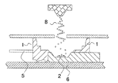
工程2.
上記塗布液を容器に入れ、循環ポンプによって塗布液を容器からノズルに搬送する。塗布液の流量はバルブによって調節する。ここで、ノズルから噴出される霧状の塗布液は、霧状で且つ螺旋状に回転されながら吹き付けられることを特徴とする。具体的には、ノズルの付近では円錐状に噴霧が広がり、ノズルから離れるにつれて円柱状に広がる。これにより、発光素子の上面、側面、および角部の全てを、膜厚がほぼ等しく且つ蛍光物質が均一に分散されてなる連続した色変換層にて覆うことができ、ブルーリング等の色むらを改善することができる。また、前記色変換層は一粒子層からなることが好ましく、これにより光の取り出し効率が向上される。本実施例では、発光素子の上面からノズル下端までの距離を40〜50mmとして円柱状に噴霧が広がった状態の所に発光素子の表面がくるように設置し、塗布液とガスとを発光素子の上面、側面および角、さらに凹部内平面上にほぼ均一な膜厚を有し連続した色変換層を形成する。
【0105】
また、上記工程は、塗布する場所を加温した状態にて行うことを特徴とする。これにより、エチルシリケートのゾル化にて生成したエタノールや溶剤を、発光素子上に吹き付けた瞬時に飛ばすことができる。これにより、発光素子へ悪影響を与えることなく色変換層を設けることができる。本実施例では、ヒーター上パッケージを載置しながらスプレーコーティングしており、前記ヒーターの温度は50℃以上300℃以下の温度に調整されていることが好ましい。
【0106】
工程3.
工程2を行った後、室温で放置すると、ゾル状エチルシリケートと空気中の水分とが反応し、SiO2により蛍光物質が固着される。
【0107】
工程4.
次に、300℃の温度で2時間乾燥させる。窒化物系発光素子は350℃以上の温度下に置かれると、発光素子としての性能が低下するため、300℃の温度下で発光素子表面への固着が可能なアルキルシリケートは、蛍光物質の固着剤として好ましく用いることができる。
【0108】
以上のように構成された発光装置は、全てが無機物にて構成されているため、高い放熱性と有すると共に近紫外や紫外線に対する耐光性にも優れている。本実施例の発光装置は、紫外域で発光する発光素子等、あらゆる素子を用いることができる。
【0109】
(実施例11)
蛍光物質として、第一の蛍光物質(Y0.995Gd0.005)2.750Al5O12:Ce0.250と第二の蛍光物質Ca1.8Eu0.2Si5N8とを混合分散させたものを用いる以外は、実施例8と同様にして発光装置を形成すると、実施例8より演色性に優れた発光装置が得られる。本実施例で用いることができる前記第二の蛍光物質は特に限定されないが、前記第一の蛍光物質と励起波長が類似であり且つ黄色から赤色の蛍光を発光することが可能なMxSiyNz:Eu(但し、MはCa、Sr、Ba、およびZnの群から選択されたアルカリ土類金属の少なくとも一種、z=(2/3)x+(4/3)y)を用いると、優れた演色性を有する光が得られ好ましい。
【0110】
具体的には、前記蛍光体は、L−M−N:R、またはL−M−O−N:R(LはBe、Mg、Ca、Sr、Ba、Znからなる群より選ばれる1種以上を含有する。MはC、Si、Ge、Sn、Ti、Zr、Hfからなる群より選ばれる1種以上を含有する。Nは窒素である。Oは酸素である。Rは希土類元素である。)で表される窒化物系蛍光体、が好ましく、さらには、LxMyN{(2/3)x+(4/3)y}:R、またはLxMyOzN{(2/3)x+(4/3)y−(2/3)z}:R(LはBe、Mg、Ca、Sr、Ba、Znからなる群より選ばれる1種以上を含有する。MはC、Si、Ge、Sn、Ti、Zr、Hfからなる群より選ばれる1種以上を含有する。Nは窒素である。Oは酸素である。Rは希土類元素である。)で表されかつ結晶構造を有する窒化物系蛍光体であることが好ましい。このような蛍光体を用いることにより暖色系の白色が発光可能な発光装置が得られる。
【0111】
具体的に基本構成元素の例を挙げると、Mu、Bが添加されたCa2Si5O0.1N7.9:Eu、Sr2Si5O0.1N7.9:Eu、(CaaSr1−a)2Si5O0.1N7.9:Eu、CaSi7O0.5N9.5:Eu、さらには希土類が添加されたCa2Si5O0.5N7.9:Eu、Sr2Si5O0.5N7.7:Eu、(CaaSr1−a)2Si5O0.1N7.9:Euなどがある。
【0112】
さらにSr2Si5N8:Eu,Pr、Ba2Si5N8:Eu,Pr、Mg2Si5N8:Eu,Pr、Zn2Si5N8:Eu,Pr、SrSi7N10:Eu,Pr、BaSi7N10:Eu,Ce、MgSi7N10:Eu,Ce、ZnSi7N10:Eu,Ce、Sr2Ge5N8:Eu,Ce、Ba2Ge5N8:Eu,Pr、Mg2Ge5N8:Eu,Pr、Zn2Ge5N8:Eu,Pr、SrGe7N10:Eu,Ce、BaGe7N10:Eu,Pr、MgGe7N10:Eu,Pr、ZnGe7N10:Eu,Ce、Sr1.8Ca0.2Si5N8:Eu,Pr、Ba1.8Ca0.2Si5N8:Eu,Ce、Mg1.8Ca0.2Si5N8:Eu,Pr、Zn1.8Ca0.2Si5N8:Eu,Ce、Sr0.8Ca0.2Si7N10:Eu,La、Ba0.8Ca0.2Si7N10:Eu,La、Mg0.8Ca0.2Si7N10:Eu,Nd、Zn0.8Ca0.2Si7N10:Eu,Nd、Sr0.8Ca0.2Ge7N10:Eu,Tb、Ba0.8Ca0.2Ge7N10:Eu,Tb、Mg0.8Ca0.2Ge7N10:Eu,Pr、Zn0.8Ca0.2Ge7N10:Eu,Pr、Sr0. 8Ca0.2Si6GeN10:Eu,Pr、Ba0.8Ca0.2Si6GeN10:Eu,Pr、Mg0.8Ca0.2Si6GeN10:Eu,Y、Zn0.8Ca0.2Si6GeN10:Eu,Y、Sr2Si5N8:Pr、Ba2Si5N8:Pr、Sr2Si5N8:Tb、BaGe7N10:Ceなどが製造できるが、これに限定されない。同様に、これらの一般式で記載された蛍光体に、所望に応じて第3成分、第4成分、第5成分等適宜、好適な元素を含有させることも当然考えられるものである。
【0113】
(実施例12)
エチルシリケートの代わりに、フッ素樹脂(PTFE=ポリテトラフルオロエチレン)を用いて塗布液を調整して蛍光体をバインドする以外は、実施例11と同様の方法により発光装置を形成すると、実施例11と同等の性能が得られ、かつ良好な製造歩留まりが得られる。
【0114】
(実施例13)
発光素子として、主波長が400nmであるLEDチップを用い、蛍光物質として(Sr0.96,Eu0.01,Mn0.03)10(PO4)6Cl2を用いる以外は実施例11と同様にして発光装置を形成する。
【0115】
ここで、上記蛍光物質の形成方法を述べる。まず、各原料であるSrHPO4、SrCO3、Eu2O3、MnCO3、NH4Clを上記組成比となるように調整し混合する。(SrHPO4:1000g、SrCO3:482.4g、Eu2O3:16.0g、MnCO3:35.2g、NH4Cl:116.5g)
【0116】
次に、上記原料を秤量しボールミル等の混合機によって乾式で充分に混合する。この混合原料をSiC、石英、アルミナなどの坩堝に詰め、N2,H2の還元雰囲気中にて960℃/hrで1200℃まで昇温し、恒温部1200℃で3時間焼成する。得られた焼成品を水中で粉砕、分散、篩過、分離、水洗、乾燥して目的の蛍光体粉末を得る。
【0117】
このようにして得られた蛍光物質を実施例10と同様にして発光素子周囲及び凹部内平面に塗布し色変換層を形成すると、高輝度に発光可能な発光装置が得られる。
【0118】
(実施例14)
原料としてCaHPO4、CaCO3、Eu2O3、MnCO3、NH4Cl、およびNH4Brを用い(Ca0.93,Eu0.05,Mn0.02)10(PO4)6Br1.0Cl1.0の組成比となるように調整、混合する。
【0119】
上記原料を秤量しボールミル等の混合機によって乾式で充分に混合する。この御合原料をSiC、石英、アルミナなどの坩堝に詰め、N2,H2の還元雰囲気中にて960℃/hrで1200℃まで昇温し、恒温部1200℃で3時間焼成する。得られた焼成品を水中で粉砕、分散、篩過、分離、水洗、乾燥して目的の蛍光体粉末を得る。この蛍光物質を用いた以外は実施例13と同様にして発光素子周囲及び凹部内平面に塗布し色変換層を形成すると、高輝度に発光可能な発光装置が得られる。
【0120】
(実施例15)
蛍光物質として、第一の蛍光物質(Y0.995Gd0.005)2.750Al5O12:Ce0.250と第二の蛍光物質(Ca0.93,Eu0.05,Mn0.02)10(PO4)6Br1.0Cl1.0とを混合分散させたものを用いる以外は、実施例13と同様にして発光装置を形成すると、高輝度に発光可能な白色光源が得られる。
【0121】
(実施例16)
(Ca0.93,Eu0.05,Mn0.02)10(PO4)6Br1.0Cl1.0蛍光物質をAl2O3からなる塗布液を発光素子周囲及び凹部内平面に上記スプレーにて塗布し第一色変換層を形成した後、前記前記第一色変換層上に接して(Y0.995Gd0.005)2.750Al5O12:Ce0.250蛍光物質を実施例11と同様の方法にてゾル状エチルシリケートを用いSiO2により固着されてなる第二色変換層を形成する以外は、実施例14と同様にして発光装置を形成する。このようにして形成することにより、第二色変換層の光屈折率<第一色変換層の光屈折率<窒化ガリウム系化合物半導体層の屈折率とすることができ、発光素子からの光の取り出し効率が高まり高出力で発光することが可能な発光装置が得られる。
【0122】
(実施例17)
ゲル状シリコーン樹脂100重量%に対し、第一の蛍光物質Y2.985Al3Ga4O12:Ce0.035を20wt%および第二の蛍光物質Ca1.8Eu0.2Si5N8を5wt%混合分散させたものを柔軟性部材として用いる以外は、実施例1と同様にして発光装置を形成すると、色温度2700Kの暖色系の白色光が得られる。
【0123】
(実施例18)
図12に示すように、第一の主面の隅部が第二の主面1cの外側からパッケージ外郭隅部に向かって露出した突出部を有し、該突出部はパッケージ外郭隅部に向かって末広がりとなる略台形形状に構成されなるパッケージを使用する以外は実施例1と同様にして発光装置を形成する。これにより、ゲル状シリコーン樹脂状にレンズを押しつけた際、パッケージの上面までゲル状シリコーン樹脂がオーバーフローすることを抑制することができる。前記突出部の数は特に限定されないが、パッケージの各隅部と対を成して形成すると、オーバーフロー効果をパッケージ全体に均一に行うことができる。
【0124】
(実施例19)
図17に示すように、第一の主面上に上面が底面よりも面積が小さい略円錐台を形成し、前記上面をレンズの支持面とする以外は、実施例1と同様にして発光装置を形成する。これにより、ゲル状シリコーン樹脂とレンズとの界面が熱膨張率差にて剥離することを抑制することができる。前記略円錐台は、等間隔に3つ以上形成されていることが好ましく、これによりさらに剥離防止効果が増大する。
【0125】
(実施例20)
図14に示すように、第一の主面上にかまぼこのような略半円柱を形成し、略半円柱の曲面の頂点ラインをレンズの支持ラインとするパッケージを使用する以外は、実施例1と同様にして発光装置を形成すると、実施例19よりもさらに剥離防止効果を高めることができ、高い信頼性を有する発光装置が得られる。前記略半円柱は、前記略円錐台と同様に、等間隔に3つ以上形成されていることが好ましく、これによりさらに効果が増大する。
【0126】
(実施例21)
図19に示すような表面実装型発光装置を形成する。金属基体に設けられた凹部内に、サブマウントをAgペーストにて固定し、前記サブマウント9上に金属バンプを用いて発光素子をフリップチップ実装する以外は、実施例1と同様にして発光装置を形成すると、光学特性および信頼性が更に向上する。ここで、前記サブマウントは、シリコン半導体からなる保護素子や窒化アルミからなる金属基体等、種々のものを用いることができる。サブマウント自体が導電性を有する場合、SiO2、SiN等の絶縁膜を介して導電性パターンを積層したものを用いることができる。また、前記金属バンプの材料は、導通可能であれば特に限定されず、Auバンプ、Sn−Pbハンダバンプ、Zn−Agハンダバンプ等を用いることができる。
【0127】
【発明の効果】
本発明の発光装置は、発光素子が載置されたパッケージを、柔軟性を有する第一の封止部材と剛性を有する第二の封止部材にて密封する際、パッケージ内部から上方まで一貫した経路を設けることにより、前記第一の封止部材と前記第二の封止部材との間に気泡が混入することを抑制することができるとともに、一度第一の封止部材中に混入されてしまった気泡をも効率よく脱泡することができる。
【図面の簡単な説明】
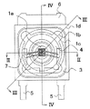
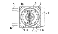
【図1】 図1は、本発明の発光装置を示す模式的平面図である。
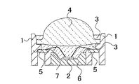
【図2】 図2は、図1のII−II線における模式的断面図である。
【図3】 図3は、図1のIII−III線における模式的断面図である。
【図4】 図4は、図1のIV−IV線における模式的断面図である。
【図5】 図5は、実施例10の発光装置を形成する一工程を示す模式的断面図である。
【図6】 図6は、実施例10の発光装置を形成する一工程を示す模式的断面図である。
【図7】 図7は、実施例10の発光装置を形成する一工程を示す模式的断面図である。
【図8】 図8は、実施例10の発光装置を形成する一工程を示す模式的断面図である。
【図9】 図9は、本発明の他の発光装置を示す模式的断面図である。
【図10】 図10は、本発明の他の発光装置を示す模式的断面図である。
【図11】 図11は、本発明の他の発光装置を示す模式的断面図である。
【図12】 図12は、本発明の他の発光装置を示す模式的断面図である。
【図13】 図13は、図12のXIII−XIII線における模式的断面図である。
【図14】 図14は、本発明の他の発光装置を示す模式的断面図である。
【図15】 図15は、図14のXV−XV線における模式的断面図である。
【図16】 図16は、本発明の他の発光装置を示す模式的断面図である。
【図17】 図17は、本発明の他の発光装置を示す模式的断面図である。
【図18】 図18は、図17のXVIII− XVIII線における模式的断面図であるである。
【図19】 図19は、本発明の他の発光装置を示す模式的断面図である。
【図20】 図20は、図19のXX−XX線における模式的断面図である。
【図21】 図21は、本発明の他の発光装置を示す模式的断面図である。
【図22】 図22は、図21のXXII−XXII線における模式的断面図である。
【図23】 図23は、本発明と比較のために示す発光装置の模式的断面図である。
【符号の説明】
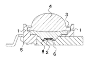
1・・・パッケージ、1a・・・パッケージ凹部、1b・・・第一の主面、1c・・・第二の主面、1d・・・第三の主面、2・・・発光素子チップ、3・・・柔軟性部材、4・・・剛性部材、5・・・リード電極、6・・・金属基体、7・・・ワイヤ、8・・・蛍光物質、9・・・サブマウント。[0001]
BACKGROUND OF THE INVENTION
The present invention relates to a light-emitting device used for various light sources such as a backlight light source, a display, and an illumination, and an optical sensor, and more particularly to a light-emitting device that combines good reliability and optical characteristics.
[0002]
[Prior art]
Today, high-luminance and high-power semiconductor light-emitting elements and small and highly sensitive light-emitting devices have been developed and used in various fields. Such a light-emitting device is utilized for, for example, a light source of an optical printer head, a light source of a liquid crystal backlight, a light source of various meters, various reading sensors, and the like, taking advantage of features such as low power consumption, small size, and light weight.
[0003]
An example of such a light emitting device is a light emitting device as shown in FIG. An LED chip is die-bonded as a light-emitting element on the
[0004]
However, such light-emitting devices have begun to be used under more severe environmental conditions due to the expansion of application fields. In a light emitting device used for an aircraft or a vehicle, for example, the temperature may change to −20 ° C. or lower and + 80 ° C. or higher depending on the outside temperature. There is also vibration at the same time as external pressure, thermal shock, and the like. In such a case, each structural member repeats expansion and contraction due to thermal stress, and the structural integrity of each component is weakened. The optical characteristics are adversely affected and the reliability is also lowered. In addition, at the present time when light emitting elements capable of emitting light with high luminance in the near ultraviolet region have been developed and used, it is important to suppress deterioration of each member due to light in the above region.
[0005]
Therefore, in recent years, a resin having a siloxane bond that is not cleaved by light has attracted attention. Such a resin has excellent light resistance with respect to the wavelength in the above region, and also has high flexibility and high stability to heat.
[0006]
However, since it has flexibility, its surface is also soft and its mechanical strength is weak, and it is not suitable as an exterior of a light-emitting device. Moreover, since it has tackiness on the surface, foreign matter adheres to it and is not suitable as a light emitting surface.
[0007]
Japanese Patent Application Laid-Open No. 2000-150968 discloses a light-emitting element mounted on the metal substrate using a package with excellent heat dissipation, and a member having flexibility and excellent light resistance inside the empty wall. A light-emitting device is described which is covered with a rigid cover provided with. The light emitting device configured as described above can have excellent heat resistance, light resistance, and external mechanical strength.
[0008]
[Patent Document 1]
JP 2000-150968 A
[0009]
[Problems to be solved by the invention]
However, as described above, when a flexible member is sealed with a rigid member, bubbles tend to be mixed into the flexible member during sealing. In particular, when sealed with a rigid member made of metal or glass that does not pass gas, the flexible member whose thermal stability is impaired by the bubbles cannot relax the thermal stress, and the adjacent rigid member may be damaged. . Further, when bubbles are contained in the interface between the flexible member and the rigid member, these interfaces are peeled off due to the bubbles to form an air layer, resulting in a decrease in light emission output and a change in optical characteristics.
[0010]
Accordingly, the present invention provides a light-emitting device that solves the above problems and has high reliability and stable optical characteristics.
[0011]
[Means for Solving the Invention]
A light emitting device of the present invention includes a light emitting element disposed in a recess provided in a package, a first light transmissive member covering the light emitting element, and a first light transmissive member mounted on the first light transmissive member. A second light-transmitting member, wherein the second light-transmitting member has a convex shape protruding in the direction of the light-emitting element, and a flange on the outside of the convex shape. And the flange is disposed in the recess of the package., Covered with the first translucent memberIt is characterized by that.
[0012]
When the light-emitting element chip is sealed by laminating the first light-transmissive member, which is a flexible member, and the second light-transmissive member, which is a rigid member, bubbles are easily mixed from these interfaces. Light emitting devices with bubbles will lose their integrity due to volatile explosion of bubbles at high temperatures, so reflow mounting that can be soldered to a mounting board etc. at a time cannot be performed, and mass productivity Is scarce. On the other hand, the light emitting device of the present invention has a high reliability that can solve the above-mentioned problem by specifying the shape of the rigid member and can be reflow mounted, and is also compatible with Pb-free mounting. Is possible.
[0013]
The cross-sectional shape of the back surface is not particularly limited as long as it protrudes in the direction of the light emitting element, but a V-shaped shape that is closest to the light emitting element at one point is preferable because the efficiency of preventing bubble mixing is enhanced.
[0014]
Furthermore, when the one point is the central portion of the back surface of the second translucent member, it is possible to efficiently prevent air bubbles from being mixed in the entire interface. Moreover, if this back surface is made into a curved surface and a pressure is applied to a flexible member in the back surface which has such a structure, the flow speed of the said flexible member will be accelerated and the bubble defoaming effect can be improved. Accordingly, a highly reliable light-emitting device can be formed with high productivity. Moreover, the adhesiveness with the flexible member below is improved, which is preferable. Further, when the back surface is convex, it is possible to prevent the flexible member from overflowing to the main surface side of the rigid member.
[0015]
The lower end of the rigid member has a flange that extends outward, and the side surface and the main surface of the flange are covered with the flexible member. By providing the collar portion in this way, the attaching operation of the rigid member is facilitated. Further, the adhesiveness with the flexible member is improved, and the reliability can be enhanced without adversely affecting the optical characteristics.
[0016]
The concave portion of the package includes at least a first main surface, a second main surface that extends outward above the first main surface, and a third main that extends outward above the second main surface. The flexible member is preferably provided continuously over the first main surface, the second main surface, and the lower end of the rigid member. Thereby, the integrity of each member can be maintained without using a separate adhesive, and a light emitting device with excellent reliability can be obtained. On the other hand, when each member is bonded with a small amount of adhesive or the like, the adhesive or the like is locally deteriorated by heat or light, resulting in a decrease in reliability. The local deterioration is prevented and the life of the light emitting device is extended.
[0017]
The second main surface is a main surface of at least three or more support bases provided apart from each other on the first main surface, and one back surface of the rigid member is in contact with the second main surface. It is preferable. With such a configuration, even if the rigid member and the flexible member are peeled off when used in a severe environment, the peeled portion can be controlled near the support base, and the optical characteristics can be maintained. .
[0018]
The rigid member is inscribed with at least three or more contacts in the outline of the second main surface, and the first main surface and the second main surface are respectively in the rigid member. It is preferable to have an exposed part outside between each contact. The light-emitting device configured as described above uses the pressure when the rigid member is placed on the flexible member, and the rigid member positioned with high accuracy by the second main surface and the first main surface Due to the action of the exposed portion of the light emitting device, air bubbles mixed in the flexible member or the interface between the flexible member and the rigid member are discharged to the outside, and a light emitting device having high reliability and stable optical characteristics is made an easy technique with high yield. Can be obtained. In many cases, the surface of the flexible member has a shape in which the central portion has an upward convexity due to surface tension in the applied state before curing, and this convex portion is pressed by one back surface to flow through the package concave portion. Thereby, the bubble defoaming action can be applied to the entire flexible member. The light emitting device of the present invention is integrally formed with the rigid member using a flexible member that overflows during the defoaming action. Moreover, it is preferable that the main surface of a rigid member has a curved surface which protruded on the opposite side to the back surface. The light emitting surface having such a shape can collect the light reflected and scattered by the inner wall of the concave portion and increase the luminance in the front direction. In particular, the back surface having a curved surface protruding in the concave direction as described above is incident on the rigid member in a state where light is diffused. Therefore, a curved surface protruding to the opposite side of the back surface is provided on the main surface side. Is preferably condensed.
[0019]
Furthermore, the lower end of the rigid member has an eaves portion that extends outward, the side surface and the main surface of the eave portion are covered with the flexible member, and the back surface of the eave portion is connected to the second main surface. It is preferable to be parallel and opposed to each other, whereby the positioning accuracy between the rigid member and the second main surface is improved, and a highly reliable light-emitting device without causing an optical axis shift between the light-emitting devices. It can be provided with good mass productivity.
[0020]
When the outline of the second main surface is a polygon having more corners than the outline of the rigid member, a small light emitting device capable of high-density mounting is obtained.
[0021]
If the outline of the rigid member is rounded at the contact point, the speed of overflowing the flexible member to the second main surface is increased, and the rigid member can be quickly fixed. Thereby, the stress which concerns on a flexible member becomes strong, a defoaming effect | action improves and reliability increases. Furthermore, the flexible member provided over the second main surface and the lower end portion of the rigid member becomes a gentle and flat main surface, and a preferable appearance is obtained.
[0022]
In the first main surface, the exposed portion is preferably a convex portion protruding outward from the central region. By setting it as such a shape, a flexible member can be efficiently flowed to a 2nd main surface and a rigid member lower end part efficiently. Moreover, the defoaming effect | action of a flexible member is improved because a flexible member collides with the said convex part wall surface. When the convex portion faces the corner of the second main surface, a flexible member having a uniform film thickness can be formed on the exposed portion of the second main surface, and structurally integrated. Sexuality can be strengthened. Further, when the tip of the convex portion is rounded, the effect is further increased.
[0023]
When the package is one in which a pair of lead electrodes is inserted from the side surface and is integrally molded with a molding resin, the inner portion of the lead electrode is along the outline of the first main surface on the first main surface. Are preferably exposed. Since the surface of the lead electrode is a metal, it is considered that the fluidity of the flexible member is excellent. The present invention has a high reliability by causing the flexible member to collide and recoil on each side wall of the package to flow upward, but the lead electrode is arranged along the side wall where the collision recoil is performed. If provided, the impact reaction speed of the flexible member is accelerated, and the effect of the bubble defoaming action is enhanced.
[0024]
The inner portion of the lead electrode is preferably provided separately from the exposed portion of the first main surface in two inner directions, thereby further improving the above effects. Also, the integrally formed lead electrode is prevented from coming off. In addition, when it is necessary to place another element such as a protective element, the element is placed at a position that does not participate in the light emission observation plane when it is electrically connected by being placed between the separate branch leads. Is preferable.
[0025]
It is preferable that a part of the back surface of the inner part of the lead electrode is exposed from a minute hole penetrating from the back side of the package. Thereby, the stress of the lead electrode received when wire bonding is performed or when the rigid member is placed can be relieved. Thereby, structural integration of a lead electrode and each member can be strengthened.
[0026]
Preferably, the package has a metal substrate whose back surface is a mounting surface, the main surface of the metal substrate is exposed from the bottom surface of the recess, and the light emitting element is mounted on the metal substrate. Thereby, heat generated from the light emitting element can be radiated to the mounting substrate satisfactorily, and the reliability of the flexible member covering the light emitting element can be improved. In addition, the fluidity of the lower flexible member can be improved on the surface of the metal substrate, and local deterioration in the vicinity of the light emitting element can be prevented.
[0027]
It is preferable that the metal substrate is inserted from the side surface direction and integrally formed with the lead electrode with the molding resin, and one end portion projects from the side surface of the package. Thereby, the contact area with the external air of a metal base | substrate increases, and the heat dissipation of a light-emitting device can be improved.
[0028]
The metal substrate preferably has a first main surface exposed from the recess and a second main surface buried in the package. This improves the structural integrity of the light emitting device.
[0029]
It is preferable to provide a second recess at the center of the main surface of the metal base exposed from the bottom surface of the recess, and place the light emitting element on the bottom surface of the second recess. This improves the extraction efficiency of light emitted from the end face of the light emitting element, prevents bubbles from entering the flexible member, defoams the mixed bubbles, and provides flexibility in the vicinity of the light emitting element when using the light emitting device. The fluidity of the adhesive member is also improved. In addition, the contact area between the flexible member and the metal substrate serving as the heat dissipation path is increased, and local deterioration of the flexible member can be prevented.
[0030]
One end of the pair of lead electrodes is preferably exposed in parallel at a predetermined distance from the side opposite to the side where the one end of the metal substrate is exposed. Thereby, the electrode wiring of the mounting substrate can be simplified. In addition, the light emitting device can be reduced in size while maintaining the back surface area of the metal substrate. Further, by providing a notch portion on the opposite side surface side on the back surface of the package, even if there are too many conductive members provided on the back surface of the metal base, the notch that the conductive member flows out in the lead electrode direction. Therefore, it is possible to prevent the lead electrode from flowing out to the opposite lead electrode and improve the yield.
[0031]
When the light emitting element has a pair of positive and negative electrodes on the same plane side, and the pair of positive and negative electrodes are respectively bridged with the inner part of the pair of lead electrodes by a wire, the vertex of the wire is the first main electrode. It is preferable to arrange | position between a surface and said 2nd main surface. By providing the wire in this way, the fluidity of the flexible member can be improved and the influence of thermal stress on the wire can be minimized. In addition, since the lead electrode is disposed above each electrode of the light emitting element and there is no obstacle protruding upward at the wire passing point from the light emitting element to the lead electrode, the wire bonding operation is relatively easy and reliable. It can be done with high performance.
[0032]
The flexible member may contain a fluorescent material. When the flexible member is configured by a laminated structure including at least two layers, the fluorescent material may be contained in at least one layer. That's fine.
[0033]
DETAILED DESCRIPTION OF THE INVENTION
As a result of various experiments, the present inventor has found that the above problem can be solved by specifying the shape of the rigid member member when the light emitting element chip is covered with the flexible member and the rigid member. Invented the invention. Hereafter, each structure of this invention is explained in full detail.
[0034]
(Package 1)
For example, as shown in FIG. 1, the package has a positive lead electrode, a negative
[0035]
More specifically, the package has a first recess on the main surface side, and the main surface of the
[0036]
On the other hand, a first main surface extending outwardly above the first concave portion and a second main surface extending outwardly above the first main surface are provided. The main surfaces of the pair of positive and negative lead electrodes inserted from the other side surface facing the one side surface of the package are exposed from the first main surface. The main surface of the lead electrode is electrically connected to each electrode of the light emitting element by a wire. The second main surface serves to position a rigid member placed on the upper side.
[0037]
Using a package having such a configuration, a light emitting element is electrically connected to the bottom surface of the recess of the package, and these are used as a flexible member as a first sealing member and a rigid member as a second sealing member. And sealed to obtain the light emitting device of the present invention.
[0038]
Here, it is sufficient that the lead electrode main surface exposed at the first recess has an area necessary for fixing a conductive wire to be cross-linked with each electrode of the light emitting element chip as shown in FIG. Other lead electrode main surfaces are preferably covered with the same material as the package resin. Thereby, the vaporization expansion which arises in the interface of a lead electrode and a 1st sealing member can be suppressed. Further, by increasing the contact area between the package molding resin having relatively high adhesiveness and the sealing member, the light emitting device can be integrated and a light emitting device with high optical characteristics and reliability can be obtained.
[0039]
Here, the package of the present embodiment has a shape that allows the first main surface and a part of the second main surface to be exposed to the outside from the second sealing member. In the present embodiment, the outer wall of the second main surface is a rounded square, a second sealing member whose outer shape is a circle is inscribed in the square, and the outer periphery of the second sealing member At four places, both the edge of the second main surface and the edge of the first main surface are exposed. As described above, the present invention provides a consistent passage from the bottom surface of the package to the upper side without being blocked by the rigid member when the rigid member is placed on the upper side after sealing the flexible member inside the package. Bubbles are also pushed out together with the flexible member from the passage, and bubbles can be prevented from being mixed between the rigid member and the flexible member. Particularly in the present embodiment, the exposed portion of the first main surface is a convex shape protruding from the central portion of the first main surface, so that the bubble defoaming effect due to the collision reaction by the outer contour of the convex shape Has improved. In the present embodiment, such a consistent passage is formed by adjusting the form of the package, but the present invention is not limited to this, and it can also be formed by forming a notch at the edge of the lens.
[0040]
(Lead electrode 5)
The lead electrode can be configured using a high thermal conductor such as copper or iron-containing copper. In addition, in order to improve the reflectance of light from the light emitting element and to prevent oxidation of the lead base material, the surface of the lead electrode can be subjected to metal plating such as silver, aluminum, copper or gold. In order to improve the reflectance of the surface, smoothing is preferable. In addition, it is preferable to increase the area of the lead electrode. In this way, heat dissipation can be improved, and the temperature rise of the light emitting element chip to be arranged can be effectively suppressed. Accordingly, a relatively large amount of power can be input to the light emitting element chip, and the light output can be improved.
[0041]
The lead electrode is formed, for example, by punching a long metal plate made of a copper alloy metal having a thickness of 0.15 mm. In the present embodiment, the press working is performed so that the positive lead electrode and the negative lead electrode are connected in one direction.
[0042]
In the light emitting device of the present invention, it is preferable that the angle between the back surface and the side surface of the lead electrode is curved. As described above, when the end of the lead electrode is rounded in accordance with the direction of injecting the resin, the flow of the molding resin becomes smooth, and the adhesion between the lead electrode and the molding resin portion is enhanced. Further, the resin can be filled in the space between the pair of lead electrodes exposed on the bottom surface of the package without any gap. Further, the joining line with the lead electrode of the molded resin portion has a shape corresponding to the lead electrode. Therefore, when the lead electrode having the above-described shape is used, the joining line with the back surface on the side surface of the molded resin portion can have a concave shape with a curved base angle. Thereby, stress concentration in the joining line can be avoided and generation of package cracks can be suppressed.
[0043]
Furthermore, it is preferable that the angle between the main surface and the side surface of the lead electrode rises to an acute angle. Thereby, the adhesiveness of a lead electrode and a 1st sealing member is improved, and peeling at these interfaces can be suppressed.
[0044]
In addition, the outer lead part of the positive lead electrode and negative lead electrode protruding from the outer wall of the package molded body is processed into a gull wing type so that the back surface is flush with the back surface of the molded resin portion and the back surface of the metal substrate. It is a positive and negative connection terminal portion. In addition, the structure of the connection terminal part of this invention is not restricted to a gull wing type | mold, Other structures, such as J-bend (Bend), may be sufficient.
[0045]
(Metal base 6)
The package used for the light-emitting device of this embodiment has a metal substrate in the center that can accommodate the light-emitting element and can efficiently dissipate heat generated from the light-emitting element. The metal base has a recess on the main surface side, and the back surface is located on substantially the same plane as the mounting surface of the light emitting device, that is, the back surface of the connecting terminal portion of the lead electrode and the back surface of the molded resin portion, It is configured to touch. With this configuration, heat generated from the light emitting element can be directly radiated to the mounting substrate, and the amount of current dropped on the light emitting element can be increased to improve output. The film thickness of the bottom surface of the recess is formed in a thin film so as to have good heat dissipation. The concave portion is preferably located in the central portion of the light emitting device, whereby good directivity characteristics can be obtained. Moreover, it is preferable that a recessed part has a volume which can accommodate the said light emitting element whole. Thereby, the light emitted from the four side surfaces of the light emitting element can be favorably extracted in the front direction through the inner wall of the recess. In addition, when the wavelength of the light emitting element is converted using the color conversion layer, the entire light emitting element arranged in the concave portion can be easily covered with the color conversion layer. The color conversion layer includes a translucent member and a fluorescent material capable of absorbing a part of light emitted from the light emitting element and emitting other wavelengths. Since the metal package used in the present invention is particularly excellent in heat dissipation of the concave portion in which the light emitting element is disposed, each member of the color conversion layer is not limited to an inorganic material, and an organic material can be used. The organic matter hardly deteriorates due to the above, and good optical characteristics can be obtained. Moreover, it is preferable that the inner wall of the said recessed part is a taper shape so that a volume may become so large that it goes to the opening side, and, thereby, the light-emitting device which can light-emit with higher brightness | luminance is obtained.
[0046]
The concave portion is formed by, for example, drawing a metal flat plate. In the present embodiment, the metal plate is drawn from the main surface direction of the metal flat plate to flow the metal in the back surface direction to form the recess. As a result, the outer shell of the back surface has an uneven shape, the contact area with the molded resin portion is increased, and the structural integrity can be enhanced.
[0047]
The thermal conductivity of the lead electrode and the metal substrate is preferably in the range of 10 W / m · K to 100 W / m · K, more preferably 15 W / m · K to 80 W / m · K, further Preferably, it is 15 W / m · K or more and 50 W / m · K or less. A light emitting device capable of supplying a large current for a long time while maintaining reliability can be obtained.
[0048]
(Light emitting element 2)
The light-emitting element chip used in the present invention is not particularly limited. However, when the pair of lead electrodes and the metal substrate are insert-molded with a molding resin as described above, the light-emitting element has a pair of positive and negative electrodes on the same surface side. A chip is used. In addition, when a fluorescent material is used, a semiconductor light emitting element having a light emitting layer capable of emitting an emission wavelength capable of exciting the fluorescent material is preferable. Examples of such semiconductor light emitting devices include various semiconductors such as ZnSe and GaN, but nitride semiconductors (InXAlYGa1-XYN, 0 ≦ X, 0 ≦ Y, and X + Y ≦ 1) are preferable. If desired, the nitride semiconductor may contain boron or phosphorus. Examples of the semiconductor structure include a homostructure having a MIS junction, a PIN junction, and a pn junction, a heterostructure, and a double heterostructure. Various emission wavelengths can be selected depending on the material of the semiconductor layer and the degree of mixed crystal. In addition, a single quantum well structure or a multiple quantum well structure in which the semiconductor active layer is formed in a thin film in which a quantum effect is generated can be used. When a nitride semiconductor is used, materials such as sapphire, spinel, SiC, Si, ZnO, and GaN are preferably used for the semiconductor substrate. In order to form a nitride semiconductor with good crystallinity with high productivity, it is preferable to use a sapphire substrate. A nitride semiconductor can be formed on the sapphire substrate by MOCVD or the like. A buffer layer of GaN, AlN, GaAIN or the like is formed on the sapphire substrate, and a nitride semiconductor having a pn junction is formed thereon. As an example of a light emitting device having a pn junction using a nitride semiconductor, a first contact layer formed of n-type gallium nitride, a first cladding layer formed of n-type aluminum nitride / gallium, and a nitride layer on a buffer layer Examples include a double hetero structure in which an active layer formed of indium gallium, a second cladding layer formed of p-type aluminum nitride / gallium, and a second contact layer formed of p-type gallium nitride are sequentially stacked. Nitride semiconductors exhibit n-type conductivity without being doped with impurities. When forming a desired n-type nitride semiconductor, for example, to improve luminous efficiency, it is preferable to appropriately introduce Si, Ge, Se, Te, C, etc. as an n-type dopant. On the other hand, when forming a p-type nitride semiconductor, the p-type dopants such as Zn, Mg, Be, Ca, Sr, and Ba are doped. Since nitride semiconductors are not easily converted to p-type by simply doping with a p-type dopant, it is preferable to reduce resistance by heating in a furnace or plasma irradiation after introducing the p-type dopant. The semiconductor substrate may be removed after laminating a metal layer on the p-type layer. When the thus configured light emitting element is mounted such that the metal layer is on the mounting surface side, a light emitting device with high heat dissipation can be obtained. A light emitting element made of a nitride semiconductor can be formed by forming each electrode on the exposed p-type layer and n-type layer and then cutting the semiconductor wafer into chips.
[0049]
In the light emitting diode of the present invention, in order to emit white light, the emission wavelength of the light emitting element is preferably 400 nm or more and 530 nm or less in consideration of the complementary color relationship with the emission wavelength from the fluorescent material, deterioration of the translucent resin, and the like. 420 nm or more and 490 nm or less is more preferable. In order to further improve the excitation and emission efficiency of the light emitting element and the fluorescent material, 450 nm or more and 475 nm or less are more preferable.
[0050]
In the present invention, since the light emitting element chip is sealed with high reliability by the first sealing member having excellent light resistance and flexibility, local deterioration of the component due to near ultraviolet rays or ultraviolet rays is suppressed. be able to. Therefore, the light-emitting device of the present invention uses a light-emitting element whose main emission wavelength is an ultraviolet region shorter than 400 nm, a fluorescent substance capable of absorbing part of light from the light-emitting element and emitting other wavelengths. By combining these, a color conversion light emitting device with little color unevenness can be obtained. Here, when the fluorescent substance is bound to the light emitting element chip, it is preferable to use a resin that is relatively resistant to ultraviolet rays, an inorganic glass, or the like.
[0051]
Here, the light emitting element is, for example, a gallium nitride compound semiconductor element capable of emitting blue light, and the element includes, for example, a nitride semiconductor layer including an n-type layer, an active layer, and a p-type layer on a sapphire substrate. An n electrode is formed on the n-type layer formed and exposed by removing a part of the active layer and the p-type layer, and a p-electrode is formed on the p-type layer.
[0052]
(Flexible member 3)
A flexible member is provided so as to cover the light emitting element from the inside of the recess of the package to the lower end of the upper rigid member. In addition to protecting the light emitting element from moisture and the like, the flexible member has translucency and can efficiently extract light from the light emitting element to the outside. Moreover, since it has high stability with respect to heat, it is possible to relieve thermal stress generated during operation of the light emitting device. Further, when a light emitting element in the near ultraviolet region or the ultraviolet region is used, it is preferable to use a flexible member having excellent light resistance against these lights. Examples of these flexible members include rubber-like elastic resins and gel-like resins. Since these resins have a low crosslinking density or do not have a crosslinked structure, they can have good flexibility. In addition, a coloring dye or a coloring pigment can be added to give a specific filter effect to the light from the light emitting element chip.
[0053]
(Rigid member 4)
In the light emitting device of the present invention, the flexible member provided around the light emitting element is sealed with a rigid member. The rigid member used in the present invention is not particularly limited as long as it has mechanical strength and is translucent.
[0054]
In the present embodiment, the rigid member that is the light extraction window is located on the upper surface of the light emitting element disposed in the recess of the metal package, and the inside of the extension line of the inner wall of the recess and the intersection emits light. Will be involved in the face. The light emitted from the end of the light emitting element is reflected and scattered by the side surface of the recess in the flexible member, passes through the rigid member, and is extracted in the front direction. It is considered that the range in which these reflected scattered light exists is substantially within the extension line of the side surface of the recess. Therefore, a light emitting device capable of emitting desired luminance can be obtained by adjusting the shape inside the intersection to any shape. Moreover, it is preferable that the base material of the rigid member has a thermal expansion coefficient approximate to that of the molding resin forming the package body and the flexible member provided in the lower part.
[0055]
The shape of the rigid member preferably has one continuous back surface. Thereby, it becomes possible to install with high reliability without air bubbles being mixed into the interface with the flexible member. Moreover, if an edge is provided on the outer periphery of the back surface, it can be installed more reliably. The edge portion is preferably provided outside the extended line of the side surface of the concave portion in which the light emitting element is accommodated, and this makes it possible to improve the reliability without affecting the optical characteristics. On the other hand, it is preferable that the main surface side has a curved surface with a central portion protruding inside the extension line of the side surface of the recess. Thereby, the light diffused on the back side can be efficiently converged in the front direction, and the luminous intensity in the front direction can be increased. In the present invention, the rigid member is structurally integrated with each member by a flexible member that is inscribed in the outline of the second main surface and overflows through a consistent passage from the bottom surface of the recess to the main surface side. Yes. In such a rigid member, a coloring dye or a coloring pigment can be added to give a specific filter effect or the like to the light from the light emitting element chip on the inside, the main surface side surface, and the back surface side.
[0056]
(Fluorescent substance 8)
In the present invention, the flexible member and the rigid member may contain other substances such as the
[0057]
In the present invention, various fluorescent materials such as an inorganic fluorescent material and an organic fluorescent material can be contained in each constituent member. As an example of such a fluorescent substance, there is a phosphor containing a rare earth element which is an inorganic phosphor. As the rare earth element-containing phosphor, specifically, at least one element selected from the group of Y, Lu, Sc, La, Gd, and Sm, and at least one selected from the group of Al, Ga, and In And a garnet-type phosphor having an element. In particular, yttrium-aluminum oxide phosphors activated with cerium are preferable, and in addition to Ce, Tb, Cu, Ag, Au, Fe, Cr, Nd, Dy, Ni, Ti, Eu, and Pr may be used as desired. Etc. can also be contained.
[0058]
In the light-emitting device of this example, fluorescence based on a cerium-activated yttrium-aluminum oxide-based fluorescent material that can emit light by exciting light emitted from a semiconductor light-emitting element having a nitride-based semiconductor as a light-emitting layer. The substance is used.
[0059]
As a specific yttrium / aluminum oxide fluorescent material, YAlO3: Ce, Y3Al5O12: Ce (YAG: Ce) or Y4Al2O9: Ce, and also a mixture thereof. The yttrium / aluminum oxide phosphor may contain at least one of Ba, Sr, Mg, Ca, and Zn. Moreover, by containing Si, the reaction of crystal growth can be suppressed and the particles of the fluorescent material can be aligned.
[0060]
In this specification, the yttrium / aluminum oxide phosphor activated by Ce is to be interpreted in a broad sense, and a part or all of yttrium is selected from the group consisting of Lu, Sc, La, Gd and Sm. Or a part or all of aluminum is used in a broad sense including a phosphor having a fluorescent action in which any one or both of Ba, Tl, Ga, and In are substituted.
[0061]
More specifically, the general formula (YzGd1-z)ThreeAlFiveO12: Photoluminescence phosphor represented by Ce (where 0 <z ≦ 1) or a general formula (Re1-aSma)ThreeRe ’FiveO12: Ce (where 0 ≦ a <1, 0 ≦ b ≦ 1, Re is at least one selected from Y, Gd, La, Sc, and Re ′ is at least one selected from Al, Ga, In) The photoluminescence phosphor shown in FIG.
[0062]
Since this fluorescent material has a garnet structure (garnet-type structure), it is resistant to heat, light and moisture, and the peak of the excitation spectrum can be made around 450 nm. The emission peak is also in the vicinity of 580 nm and has a broad emission spectrum that extends to 700 nm.
[0063]
Further, the photoluminescence phosphor can increase the excitation light emission efficiency in a long wavelength region of 460 nm or more by containing Gd (gadolinium) in the crystal. As the Gd content increases, the emission peak wavelength shifts to a longer wavelength, and the entire emission wavelength also shifts to the longer wavelength side. That is, when a strong reddish emission color is required, it can be achieved by increasing the amount of Gd substitution. On the other hand, as Gd increases, the emission luminance of photoluminescence by blue light tends to decrease. Furthermore, in addition to Ce, Tb, Cu, Ag, Au, Fe, Cr, Nd, Dy, Co, Ni, Ti, Eu, and the like can be contained as desired.
[0064]
Moreover, in the composition of the yttrium / aluminum / garnet (garnet) phosphor having a garnet structure, the emission wavelength is shifted to the short wavelength side by substituting part of Al with Ga. Further, by substituting part of Y in the composition with Gd, the emission wavelength is shifted to the longer wavelength side.
[0065]
When substituting a part of Y with Gd, it is preferable that the substitution with Gd is less than 10%, and the Ce content (substitution) is 0.03 to 1.0. If the substitution with Gd is less than 20%, the green component is large and the red component is small. However, by increasing the Ce content, the red component can be supplemented and a desired color tone can be obtained without lowering the luminance. With such a composition, the temperature characteristics are good and the reliability of the light emitting diode can be improved. In addition, when a photoluminescent phosphor adjusted to have a large amount of red component is used, a light emitting device capable of emitting an intermediate color such as pink can be formed.
[0066]
Such photoluminescent phosphors use oxides or compounds that easily become oxides at high temperatures as raw materials for Y, Gd, Al, and Ce, and mix them well in a stoichiometric ratio. Get raw materials. Alternatively, a mixed raw material obtained by mixing a coprecipitation oxide obtained by firing a solution obtained by coprecipitation of a solution obtained by dissolving a rare earth element of Y, Gd, and Ce in an acid in a stoichiometric ratio with oxalic acid and aluminum oxide. Get. A suitable amount of fluoride such as barium fluoride or ammonium fluoride is mixed as a flux and packed in a crucible, and fired in air at a temperature range of 1350 to 1450 ° C. for 2 to 5 hours to obtain a fired product, and then fired. The product can be obtained by ball milling in water, washing, separating, drying and finally passing through a sieve.
[0067]
In the light emitting device of the present invention, such a photoluminescent phosphor may be a mixture of yttrium, aluminum, garnet (garnet type) phosphor activated with two or more kinds of cerium, and other phosphors. .
[0068]
The particle size of the fluorescent material used in the present invention is preferably in the range of 10 μm to 50 μm, more preferably 15 μm to 30 μm. A fluorescent material having a particle size of less than 15 μm is relatively easy to form an aggregate, and is densely settled in a liquid resin, thus reducing the light transmission efficiency. In the present invention, by using such a fluorescent material that does not have a fluorescent material, concealment of light by the fluorescent material is suppressed and the output of the light emitting device is improved. In addition, the fluorescent material having a particle size range of the present invention has high light absorption and conversion efficiency and a wide excitation wavelength range. Thus, by including a large particle size fluorescent material having optically excellent characteristics, light around the dominant wavelength of the light emitting element can be converted and emitted well, and the mass productivity of the light emitting device is improved. Is done.
[0069]
Here, in the present invention, the particle size is a value obtained from a volume-based particle size distribution curve. The volume-based particle size distribution curve is obtained by measuring the particle size distribution by a laser diffraction / scattering method. Specifically, in an environment of an air temperature of 25 ° C. and a humidity of 70%, hexametalin having a concentration of 0.05%. Each substance was dispersed in an aqueous sodium acid solution and measured with a laser diffraction particle size distribution analyzer (SALD-2000A) in a particle size range of 0.03 μm to 700 μm. In this volume-based particle size distribution curve, it is a particle size value when the integrated value is 50%, and the central particle size of the fluorescent material used in the present invention is preferably in the range of 15 μm to 50 μm. Moreover, it is preferable that the fluorescent substance which has this center particle size value is contained frequently, and the frequency value is preferably 20% to 50%. In this way, by using a fluorescent material with small variation in particle size, a light emitting device having a favorable color tone with suppressed color unevenness can be obtained.
[0070]
The location of the fluorescent material is not particularly limited, and a binder may be provided on the back surface of the window portion of the rigid member, or may be directly contained in each material of the rigid member and the flexible member. When the fluorescent material is attached to the back surface of the rigid member or the surface of the light emitting element with a binder, the material of the binder is not particularly limited, and either an organic material or an inorganic material can be used. When an organic substance is used as the binder, a transparent resin excellent in weather resistance such as an epoxy resin, an acrylic resin, or silicone is preferably used as a specific material. In particular, silicone is preferable because it is excellent in reliability and can improve the dispersibility of the fluorescent material.
[0071]
In addition, when a fluorescent substance is placed on the lens surface, it is preferable to use an inorganic substance that is close to the coefficient of thermal expansion as a binder because the fluorescent substance can be satisfactorily adhered. As a specific method, a precipitation method, a sol-gel method, or the like can be used. For example, fluorescent material, silanol (Si (OEt)3OH) and ethanol are mixed to form a slurry. After the slurry is discharged from the nozzle to the window of the rigid member, the slurry is heated at 300 ° C. for 3 hours to convert silanol into SiO 2.2And the fluorescent material can be fixed.
[0072]
Further, an inorganic binder can be used as a binder. The binder is a so-called low-melting glass, is a fine particle and is preferably very stable in the binder with little absorption with respect to radiation from the ultraviolet to the visible region, and was obtained by a precipitation method. Alkaline earth borates, which are fine particles, are suitable.
[0073]
In addition, when attaching a fluorescent substance having a large particle size, a binder whose particle is an ultrafine powder even if the melting point is high, such as silica, alumina made by Degussa, or a fine particle size alkali obtained by a precipitation method It is preferred to use earth metal pyrophosphates, orthophosphates and the like. These binders can be used alone or mixed with each other.
[0074]
Here, a method for applying the binder will be described. In order to sufficiently enhance the binding effect, the binder is preferably used as a binder slurry by wet pulverization in a vehicle to form a slurry. The vehicle is a high viscosity solution obtained by dissolving a small amount of a binder in an organic solvent or deionized water. For example, an organic vehicle can be obtained by adding 1 wt% of nitrocellulose as a binder to butyl acetate as an organic solvent.
[0075]
A fluorescent substance is contained in the binder slurry thus obtained to prepare a coating solution. The amount of the slurry in the coating solution is preferably such that the total amount of the binder in the slurry is about 1 to 3% wt with respect to the amount of the fluorescent substance in the coating solution. If the amount of the binder added is too large, the luminous flux maintenance factor tends to decrease. Therefore, it is preferable to minimize the amount of use.
[0076]
When it is desired to fix the fluorescent material to the back surface or the main surface of the rigid member with the binder, the coating liquid is applied to the back surface of the window portion, and then hot air or hot air is blown and dried. Finally, baking is performed at a temperature of 400 ° C. to 700 ° C. to scatter the vehicle. Thereby, the phosphor layer is adhered to the surface of the window portion with the binder.
[0077]
(Diffusion agent)
Further, in the present invention, the color conversion member may contain a diffusing agent in addition to the fluorescent material. As a specific diffusing agent, barium titanate, titanium oxide, aluminum oxide, silicon oxide or the like is preferably used. As a result, a light emitting device having good directivity can be obtained.
[0078]
Here, in this specification, the diffusing agent refers to those having a center particle diameter of 1 nm or more and less than 5 μm. A diffusing agent having a size of 1 μm or more and less than 5 μm is preferable because it diffuses light from the light-emitting element and the fluorescent material well and can suppress color unevenness that tends to occur by using a fluorescent material having a large particle size. In addition, the half width of the emission spectrum can be narrowed, and a light emitting device with high color purity can be obtained. On the other hand, a diffusing agent having a wavelength of 1 nm or more and less than 1 μm has a low interference effect on the light wavelength from the light emitting element, but has a high transparency and can increase the resin viscosity without reducing the luminous intensity. As a result, when the color conversion member is arranged by potting or the like, it becomes possible to disperse the fluorescent substance in the resin almost uniformly in the syringe and maintain the state, and the fluorescent substance having a large particle size that is relatively difficult to handle. Even when a substance is used, it is possible to produce with good yield. Thus, the action of the diffusing agent in the present invention varies depending on the particle size range, and can be selected or combined according to the method of use.
[0079]
(Filler)
Furthermore, in the present invention, the color conversion member may contain a filler in addition to the fluorescent material. The specific material is the same as that of the diffusing agent, but the diffusing agent has a central particle size different from that of the diffusing agent. In this specification, the filler has a central particle size of 5 μm or more and 100 μm or less. When the filler having such a particle size is contained in the translucent resin, the chromaticity variation of the light emitting device is improved by the light scattering action, and the thermal shock resistance of the translucent resin can be enhanced. As a result, even when used at high temperatures, it is possible to prevent disconnection of the wire that electrically connects the light emitting element and the external electrode, and peeling of the bottom surface of the light emitting element and the bottom surface of the recess of the package with high reliability. A light emitting device is obtained. Furthermore, the fluidity of the resin can be adjusted to be constant for a long time, and a sealing member can be formed in a desired place, and mass production can be performed with a high yield.
[0080]
The filler preferably has a particle size and / or shape similar to that of the fluorescent material. Here, in this specification, the similar particle diameter means a case where the difference in the central particle diameter of each particle is less than 20%, and the similar shape means an approximate degree of each particle diameter with a perfect circle. This represents a case where the difference in the value of the degree of circularity (circularity = perimeter length of a perfect circle equal to the projected area of the particle / perimeter length of the projected particle) is less than 20%. By using such a filler, the fluorescent material and the filler interact with each other, and the fluorescent material can be favorably dispersed in the resin, thereby suppressing color unevenness. Furthermore, it is preferable that both the fluorescent substance and the filler have a central particle diameter of 15 μm to 50 μm, more preferably 20 μm to 50 μm. In this way, by adjusting the particle diameter, a preferable interval is provided between the particles. be able to. As a result, a light extraction path is ensured, and the directivity can be improved while suppressing a decrease in luminous intensity due to filler mixing.
[0081]
Hereinafter, the light-emitting device of the Example which concerns on this invention is explained in full detail. In addition, this invention is not limited only to the Example shown below.
【Example】
[0082]
Example 1
A surface mount type light emitting device as shown in FIG. 1 is formed. The LED chip has a 475 nm In as a light emitting layer with a monochromatic emission peak of visible light.0.2Ga0.8A nitride semiconductor element having an N semiconductor is used. More specifically, in the LED chip, TMG (trimethyl gallium) gas, TMI (trimethyl indium) gas, nitrogen gas and dopant gas are flowed together with a carrier gas on a cleaned sapphire substrate, and a nitride semiconductor is formed by MOCVD. Can be formed. SiH as dopant gas4And Cp2A layer to be an n-type nitride semiconductor or a p-type nitride semiconductor is formed by switching Mg.
[0083]
As an element structure of the LED chip, an n-type GaN layer which is an undoped nitride semiconductor on a sapphire substrate, a GaN layer where an Si-doped n-type electrode is formed to become an n-type contact layer, and an n-type nitride semiconductor which is an
[0084]
Etching exposes the surface of each pn contact layer on the same side as the nitride semiconductor on the sapphire substrate. Positive and negative pedestal electrodes are formed on each contact layer by sputtering. A metal thin film is formed on the entire surface of the p-type nitride semiconductor as a translucent electrode, and then a pedestal electrode is formed on a part of the translucent electrode. After drawing the scribe line on the completed semiconductor wafer, it is divided by an external force to form LED chips that are semiconductor light emitting elements.
[0085]
On the other hand, a first copper plate having a thickness of 0.3 mm is punched to form a plurality of pairs of lead electrodes connected in one direction. Next, a 1.2 mm-thick second copper plate having a thickness greater than that of the first copper plate is punched and pressed, and a metal substrate having a recess capable of accommodating a light emitting element chip on the main surface side is provided. A plurality are formed. The pair of lead electrodes and the metal base are inserted from opposite directions, and are arranged in a metal mold so that the respective lead electrodes are symmetrical via the metal base above the metal base. At this time, the inner tip portion of each lead electrode is fixed by the support from below.
[0086]
In this way, the first copper plate and the second copper plate installed in the mold are integrally formed with a molding resin to create a package. The package thus obtained has a first concave portion in which the concave portion of the metal substrate is exposed on the main surface side, a first main surface that spreads outward above the first concave portion, and the first main surface. A second main surface extending outwardly above the surface. The outline of the second main surface is a square with a rounded corner, and the corners of the first main surface are provided with protrusions toward the corners of the second main surface. The protrusion is configured to be exposed to the outside of the rigid member when the rigid member is placed on the upper side.
[0087]
Next, an LED chip is die-bonded with an Ag—Sn alloy in a recess provided in the metal substrate. Here, as the bonding member used for die bonding, a resin or glass containing a conductive material can be used in addition to the above-described alloy. The conductive material contained is preferably Ag. When an Ag paste having a content of 80% to 90% is used, a light emitting device having excellent heat dissipation and low stress after bonding can be obtained. In addition, it is preferable to provide a metal layer on the substrate side of the light-emitting element and fix the light-emitting element because heat dissipation and light extraction efficiency are improved.
[0088]
Next, the respective electrodes of the die-bonded LED chip and the respective lead electrodes exposed from the bottom of the package recess are electrically connected by Ag wires. Here, when resin is not used for the constituent members, it is also possible to use Al wires.
[0089]
Next, a gel-like silicone resin is injected by potting so as to cover the second main surface from the concave portion, and then a glass lens as a light-transmitting rigid member is pressed downward onto the gel-like silicone resin. Place. Here, the lens can be made of a thermoplastic resin, glass, or the like, which is a plastic. Moreover, it has one continuous back surface and has a curved surface protruding downward. Further, the outer peripheral portion has an edge portion whose rear surface is parallel to the second main surface. Further, the outer shell of the edge portion has a circular shape so as to be inscribed in the outer shell of the second main surface. The lens configured as described above is installed on the second main surface, and a part of the gel-like silicone resin below the protruding portion of the first main surface exposed from the outside of the lens is After overflowing to the upper surface of the edge, heating is performed at 70 ° C. for 2 hours, at 100 ° C. for 2 hours, and further at 150 ° C. for 2 hours to structurally integrate the members.
[0090]
The light-emitting device obtained in this manner does not have contaminants such as bubbles and has excellent reliability and optical characteristics.
[0091]
(Example 2)
As shown in FIG. 10, when the light emitting device is formed in the same manner as in Example 1 except that the outline of the second main surface is a rounded hexagon, it is more mass-productive and denser than Example 1. A light-emitting device that can be obtained is obtained.
[0092]
(Example 3)
As shown in FIG. 11, the outline of the second main surface and the outline of the first main surface are polygons that are similar to each other, and the lens has an outer periphery so that the corners of the first main surface are exposed. When the light emitting device is formed in the same manner as in Example 1 except that the portion has a notch, the same effect as in Example 1 can be obtained.
[0093]
(Example 4)
When the light emitting device is formed in the same manner as in Example 3 except that the lens used as the rigid member has a convex lens shape, the front luminous intensity is improved by 50% compared to Example 1.
[0094]
(Example 5)
A light emitting device is formed in the same manner as in Example 1 except that a fluorescent material is previously contained in the lens.
[0095]
Here, as the fluorescent material, a solution obtained by dissolving rare earth elements of Y, Gd, and Ce in acid at a stoichiometric ratio is coprecipitated with oxalic acid. A co-precipitated oxide obtained by firing this and aluminum oxide are mixed to obtain a mixed raw material. This is mixed with barium fluoride as a flux and packed in a crucible and fired in air at a temperature of 1400 ° C. for 3 hours to obtain a fired product. The fired product is ball-milled in water, washed, separated, dried, and finally passed through a sieve to have a center particle size of 22 μm (Y0.995Gd0.005)2.750Al5O12: Ce0.250Form a fluorescent material.
[0096]
The fluorescent substance thus obtained and powdered silica are mixed at a ratio of 1: 2, and melt-cured in a mold and collectively molded. The color conversion type light-emitting device obtained in this way can achieve the same effects as those of Example 1, and can emit white light with high reliability and high output.
[0097]
(Example 6)
A color conversion member is constituted by containing 50 wt% of the fluorescent material in a slurry composed of 90 wt% of nitrocellulose and 10 wt% of γ-alumina, coating the back surface of the rigid member, and heating and curing at 220 ° C. for 30 minutes. Except for the above, when the light emitting device is formed in the same manner as in Example 5, the same effect as in Example 5 is obtained.
[0098]
(Example 7)
When the light emitting device is formed in the same manner as in Example 1 except that the elastic silicone resin is applied on the gel silicone resin and then the lens is placed, the adhesion of the lens is improved. A light emitting device with higher reliability than 1 can be obtained.
[0099]
(Example 8)
When the light emitting device is formed in the same manner as in Example 7 except that the gel-like silicone resin contains 50 wt% of the fluorescent material, the same effect as in Example 5 can be obtained.
[0100]
Example 9
When the light emitting device is formed in the same manner as in Example 1 except that the light emitting element is sealed in advance with silica gel containing 50 wt% of the fluorescent material, the same effect as in Example 5 is obtained.
[0101]
(Example 10)
The surface of the light emitting element is coated with the fluorescent material and SiO.2A light-emitting device is formed in the same manner as in Example 1 except that a continuous color conversion layer having s is formed by spray coating. Here, a method for forming the color conversion layer will be described in detail.
[0102]
As the alkyl silicate, methyl silicate, ethyl silicate, N-propyl silicate, N-butyl silicate can be used.2A colorless and transparent oligomer liquid condensed with ethyl silicate containing 40 wt% is used. In addition, ethyl silicate is used that has been previously reacted with water in the presence of a catalyst to undergo a hydrolysis reaction to form a sol.
[0103]
First, a coating solution is prepared by stirring a solution in which sol-form ethylsilicate, ethylene glycol, and a fluorescent substance are mixed at a weight ratio of 1: 1: 1. Here, since sol-like ethylsilicate is easy to dry, it is preferable to prevent gelation by mixing with a high boiling point (100 ° C. to 200 ° C.) organic solvent such as butanol or ethylene glycol. When mixed with a high-boiling organic solvent in this way, clogging of the nozzle tip due to gelation of the sol-like ethyl silicate can be prevented and work efficiency can be improved.
[0104]
The coating liquid is placed in a container, and the coating liquid is conveyed from the container to the nozzle by a circulation pump. The flow rate of the coating solution is adjusted by a valve. Here, the mist-like coating liquid ejected from the nozzle is sprayed while being rotated in a mist-like and spiral manner. Specifically, the spray spreads in a conical shape in the vicinity of the nozzle, and spreads in a cylindrical shape as the distance from the nozzle increases. Accordingly, the upper surface, side surfaces, and corners of the light emitting element can be covered with a continuous color conversion layer in which the film thickness is substantially equal and the fluorescent material is uniformly dispersed, and color unevenness such as blue ring is obtained. Can be improved. The color conversion layer is preferably composed of a single particle layer, which improves the light extraction efficiency. In this embodiment, the distance from the upper surface of the light emitting element to the lower end of the nozzle is set to 40 to 50 mm so that the surface of the light emitting element is placed in a state where the spray spreads in a columnar shape, and the coating liquid and the gas are put into the light emitting element. A continuous color conversion layer having a substantially uniform film thickness is formed on the upper surface, side surfaces and corners of the substrate, and on the inner surface of the recess.
[0105]
Moreover, the said process is performed in the state which heated the place to apply | coat. As a result, the ethanol or solvent generated by the sol-formation of ethyl silicate can be instantaneously blown onto the light emitting element. Accordingly, the color conversion layer can be provided without adversely affecting the light emitting element. In this embodiment, spray coating is performed while placing the package on the heater, and the temperature of the heater is preferably adjusted to a temperature of 50 ° C. or higher and 300 ° C. or lower.
[0106]
After performing
[0107]
Next, it is dried at a temperature of 300 ° C. for 2 hours. When nitride-based light-emitting elements are placed at a temperature of 350 ° C. or higher, the performance as light-emitting elements deteriorates. Therefore, alkylsilicates that can be fixed to the surface of light-emitting elements at a temperature of 300 ° C. It can be preferably used as an agent.
[0108]
Since all the light emitting devices configured as described above are made of an inorganic material, the light emitting device has high heat dissipation and is excellent in light resistance against near ultraviolet rays and ultraviolet rays. The light emitting device of this embodiment can use any element such as a light emitting element that emits light in the ultraviolet region.
[0109]
(Example 11)
As the fluorescent material, the first fluorescent material (Y0.995Gd0.005)2.750Al5O12: Ce0.250And second fluorescent substance Ca1.8Eu0.2Si5N8When a light emitting device is formed in the same manner as in Example 8 except that a mixture of and dispersed is used, a light emitting device having better color rendering than in Example 8 is obtained. The second fluorescent material that can be used in this embodiment is not particularly limited, but MxSiyNz: Eu () having an excitation wavelength similar to that of the first fluorescent material and capable of emitting yellow to red fluorescence. However, when M is at least one alkaline earth metal selected from the group of Ca, Sr, Ba, and Zn, z = (2/3) x + (4/3) y), an excellent color rendering property is obtained. The light which has is obtained and is preferable.
[0110]
Specifically, the phosphor is LMN: R or LMON: R (L is one selected from the group consisting of Be, Mg, Ca, Sr, Ba, Zn). M contains at least one selected from the group consisting of C, Si, Ge, Sn, Ti, Zr, and Hf, N is nitrogen, O is oxygen, and R is a rare earth element. Nitride-based phosphors represented by the following formula:xMyN{(2/3) x + (4/3) y}: R or LxMyOzN{(2/3) x + (4/3) y- (2/3) z}: R (L contains at least one selected from the group consisting of Be, Mg, Ca, Sr, Ba, Zn. M is selected from the group consisting of C, Si, Ge, Sn, Ti, Zr, Hf) 1 or more, N is nitrogen, O is oxygen, R is a rare earth element), and is preferably a nitride-based phosphor having a crystal structure. By using such a phosphor, a light emitting device capable of emitting warm white light can be obtained.
[0111]
Specific examples of basic constituent elements include Ca and Mu and B added.2Si5O0.1N7.9: Eu, Sr2Si5O0.1N7.9: Eu, (CaaSr1-a)2Si5O0.1N7.9: Eu, CaSi7O0.5N9.5: Eu, and further Ca added with rare earth2Si5O0.5N7.9: Eu, Sr2Si5O0.5N7.7: Eu, (CaaSr1-a)2Si5O0.1N7.9: Eu etc.
[0112]
Furthermore, Sr2Si5N8: Eu, Pr, Ba2Si5N8: Eu, Pr, Mg2Si5N8: Eu, Pr, Zn2Si5N8: Eu, Pr, SrSi7N10: Eu, Pr, BaSi7N10: Eu, Ce, MgSi7N10: Eu, Ce, ZnSi7N10: Eu, Ce, Sr2Ge5N8: Eu, Ce, Ba2Ge5N8: Eu, Pr, Mg2Ge5N8: Eu, Pr, Zn2Ge5N8: Eu, Pr, SrGe7N10: Eu, Ce, BaGe7N10: Eu, Pr, MgGe7N10: Eu, Pr, ZnGe7N10: Eu, Ce, Sr1.8Ca0.2Si5N8: Eu, Pr, Ba1.8Ca0.2Si5N8: Eu, Ce, Mg1.8Ca0.2Si5N8: Eu, Pr, Zn1.8Ca0.2Si5N8: Eu, Ce, Sr0.8Ca0.2Si7N10: Eu, La, Ba0.8Ca0.2Si7N10: Eu, La, Mg0.8Ca0.2Si7N10: Eu, Nd, Zn0.8Ca0.2Si7N10: Eu, Nd, Sr0.8Ca0.2Ge7N10: Eu, Tb, Ba0.8Ca0.2Ge7N10: Eu, Tb, Mg0.8Ca0.2Ge7N10: Eu, Pr, Zn0.8Ca0.2Ge7N10: Eu, Pr, Sr0. 8Ca0.2Si6GeN10: Eu, Pr, Ba0.8Ca0.2Si6GeN10: Eu, Pr, Mg0.8Ca0.2Si6GeN10: Eu, Y, Zn0.8Ca0.2Si6GeN10: Eu, Y, Sr2Si5N8: Pr, Ba2Si5N8: Pr, Sr2Si5N8: Tb, BaGe7N10: Ce can be produced, but is not limited thereto. Similarly, it is naturally conceivable that the phosphors described by these general formulas appropriately contain suitable elements such as the third component, the fourth component, and the fifth component as desired.
[0113]
Example 12
When a light emitting device was formed by the same method as in Example 11 except that the phosphor was bound by adjusting the coating solution using a fluororesin (PTFE = polytetrafluoroethylene) instead of ethyl silicate, Example 11 And a good production yield can be obtained.
[0114]
(Example 13)
An LED chip having a dominant wavelength of 400 nm is used as the light emitting element, and (Sr0.96, Eu0.01, Mn0.03)10(PO4)6Cl2A light emitting device is formed in the same manner as in Example 11 except that is used.
[0115]
Here, a method for forming the fluorescent material will be described. First, each raw material SrHPO4, SrCO3, Eu2O3, MnCO3, NH4Adjust and mix Cl so as to have the above composition ratio. (SrHPO4: 1000g, SrCO3: 482.4 g, Eu2O3: 16.0 g, MnCO3: 35.2 g, NH4Cl: 116.5 g)
[0116]
Next, the raw materials are weighed and thoroughly mixed by a dry method using a mixer such as a ball mill. This mixed raw material is packed in a crucible such as SiC, quartz, or alumina, and N2, H2In a reducing atmosphere, the temperature is raised to 1200 ° C. at 960 ° C./hr, and firing is performed at a constant temperature portion of 1200 ° C. for 3 hours. The obtained fired product is pulverized, dispersed, sieved, separated, washed with water and dried in water to obtain the desired phosphor powder.
[0117]
When the fluorescent material thus obtained is applied to the periphery of the light emitting element and the flat surface in the concave portion in the same manner as in Example 10 to form a color conversion layer, a light emitting device capable of emitting light with high luminance is obtained.
[0118]
(Example 14)
CaHPO as raw material4, CaCO3, Eu2O3, MnCO3, NH4Cl and NH4Br is used (Ca0.93, Eu0.05, Mn0.02)10(PO4)6Br1.0Cl1.0The composition ratio is adjusted and mixed.
[0119]
The raw materials are weighed and mixed thoroughly by a dry method using a mixer such as a ball mill. This goto raw material is packed in a crucible such as SiC, quartz, alumina, etc.2, H2In a reducing atmosphere, the temperature is raised to 1200 ° C. at 960 ° C./hr, and firing is performed at a constant temperature portion of 1200 ° C. for 3 hours. The obtained fired product is pulverized, dispersed, sieved, separated, washed with water and dried in water to obtain the desired phosphor powder. A light emitting device capable of emitting light with high luminance can be obtained by coating the periphery of the light emitting element and the inner surface of the recess in the same manner as in Example 13 except that this fluorescent material is used to form a color conversion layer.
[0120]
(Example 15)
As the fluorescent material, the first fluorescent material (Y0.995Gd0.005)2.750Al5O12: Ce0.250And second fluorescent material (Ca0.93, Eu0.05, Mn0.02)10(PO4)6Br1.0Cl1.0A white light source capable of emitting light with high brightness can be obtained by forming a light emitting device in the same manner as in Example 13 except that a mixture of and dispersed is used.
[0121]
(Example 16)
(Ca0.93, Eu0.05, Mn0.02)10(PO4)6Br1.0Cl1.0Fluorescent material is Al2O3After the coating liquid consisting of the above is applied by spraying on the periphery of the light emitting element and the plane in the recess to form the first color conversion layer, the first color conversion layer is contacted (Y0.995Gd0.005)2.750Al5O12: Ce0.250The fluorescent material was made of SiO in the same manner as in Example 11 using sol-like ethyl silicate.2A light emitting device is formed in the same manner as in Example 14 except that the second color conversion layer fixed by is formed. By forming in this way, the optical refractive index of the second color conversion layer <the optical refractive index of the first color conversion layer <the refractive index of the gallium nitride compound semiconductor layer, and the light from the light emitting element can be obtained. A light-emitting device capable of emitting light at high output with increased extraction efficiency can be obtained.
[0122]
(Example 17)
The first fluorescent substance Y with respect to 100% by weight of the gel silicone resin2.985Al3Ga4O12: Ce0.03520 wt% and the second fluorescent substance Ca1.8Eu0.2Si5N8When a light emitting device is formed in the same manner as in Example 1 except that 5 wt% mixed and dispersed is used as the flexible member, warm white light having a color temperature of 2700 K is obtained.
[0123]
(Example 18)
As shown in FIG. 12, the corner portion of the first main surface has a protruding portion exposed from the outside of the second
[0124]
Example 19
As shown in FIG. 17, the light emitting device is the same as in Example 1 except that a substantially truncated cone having a top surface smaller than the bottom surface is formed on the first main surface, and the top surface is used as a lens support surface. Form. Thereby, it can suppress that the interface of a gel-like silicone resin and a lens peels according to a thermal expansion coefficient difference. It is preferable that three or more of the substantially truncated cones are formed at equal intervals, which further increases the peeling prevention effect.
[0125]
(Example 20)
As shown in FIG. 14, Example 1 is used except that a substantially semicircular cylinder like a kamaboko is formed on the first main surface and a vertex line of the curved surface of the substantially semicircular cylinder is used as a lens support line. When the light emitting device is formed in the same manner as in Example 19, the effect of preventing peeling can be further enhanced as compared with Example 19, and a light emitting device having high reliability can be obtained. Like the substantially truncated cone, it is preferable that three or more substantially semicircular cylinders are formed at equal intervals, which further increases the effect.
[0126]
(Example 21)
A surface mount light emitting device as shown in FIG. 19 is formed. The light emitting device is the same as in Example 1 except that the submount is fixed with Ag paste in the recess provided on the metal substrate, and the light emitting element is flip-chip mounted on the
[0127]
【The invention's effect】
In the light emitting device of the present invention, when the package on which the light emitting element is placed is sealed with the first sealing member having flexibility and the second sealing member having rigidity, the light emitting device is consistent from the inside of the package to the upper side. By providing the path, air bubbles can be prevented from being mixed between the first sealing member and the second sealing member, and once mixed in the first sealing member. It is possible to efficiently degas bubbles that have been trapped.
[Brief description of the drawings]
FIG. 1 is a schematic plan view showing a light emitting device of the present invention.
FIG. 2 is a schematic cross-sectional view taken along the line II-II in FIG.
3 is a schematic cross-sectional view taken along line III-III in FIG. 1. FIG.
FIG. 4 is a schematic cross-sectional view taken along line IV-IV in FIG.
5 is a schematic cross-sectional view showing a step of forming the light emitting device of Example 10. FIG.
6 is a schematic cross-sectional view showing a step of forming the light emitting device of Example 10. FIG.
7 is a schematic cross-sectional view showing a step of forming the light emitting device of Example 10. FIG.
8 is a schematic cross-sectional view showing a step of forming the light emitting device of Example 10. FIG.
FIG. 9 is a schematic cross-sectional view showing another light emitting device of the present invention.
FIG. 10 is a schematic cross-sectional view showing another light emitting device of the present invention.
FIG. 11 is a schematic cross-sectional view showing another light emitting device of the present invention.
FIG. 12 is a schematic cross-sectional view showing another light emitting device of the present invention.
13 is a schematic cross-sectional view taken along line XIII-XIII in FIG.
FIG. 14 is a schematic cross-sectional view showing another light-emitting device of the present invention.
FIG. 15 is a schematic cross-sectional view taken along line XV-XV in FIG.
FIG. 16 is a schematic cross-sectional view showing another light emitting device of the present invention.
FIG. 17 is a schematic cross-sectional view showing another light emitting device of the present invention.
18 is a schematic cross-sectional view taken along line XVIII-XVIII in FIG.
FIG. 19 is a schematic cross-sectional view showing another light emitting device of the present invention.
20 is a schematic cross-sectional view taken along line XX-XX in FIG.
FIG. 21 is a schematic cross-sectional view showing another light emitting device of the present invention.
22 is a schematic cross-sectional view taken along line XXII-XXII in FIG. 21. FIG.
FIG. 23 is a schematic cross-sectional view of a light-emitting device shown for comparison with the present invention.
[Explanation of symbols]
DESCRIPTION OF
Claims (9)
前記第二の透光性部材は、前記発光素子の方向へ突出された凸形状と、その凸形状の外側に鍔部と、を有しており、前記鍔部は、前記パッケージの凹部内に配置され、前記第一の透光性部材により被覆されていることを特徴とする発光装置。A light emitting element disposed in a recess provided in the package, a first light transmissive member covering the light emitting element, and a second light transmissive member placed on the first light transmissive member; A light emitting device comprising:
The second translucent member has a convex shape protruding in the direction of the light emitting element, and a flange on the outside of the convex shape, and the flange is in the recess of the package. A light-emitting device that is disposed and covered with the first light- transmissive member .
前記第二の透光性部材は、その背面に、前記第二の主面との接点を少なくとも3つ有している請求項1に記載の発光装置。The concave portion of the package includes at least a first main surface, a second main surface that extends outward above the first main surface, and a third main that extends outward above the second main surface. And having a surface,
2. The light emitting device according to claim 1 , wherein the second translucent member has at least three contacts with the second main surface on a back surface thereof.
前記ワイヤの頂点は、前記第一主面と前記第二の主面の間に配置されている請求項2から5に記載の発光装置。The light emitting element has a pair of positive and negative electrodes on the same surface side, and these electrodes are respectively connected to a pair of positive and negative lead electrodes provided in the package via wires,
The apex of the wire, the light emitting device according to 5 claim 2 which is disposed between the second major surface and the first major surface.
前記第一の主面は、複数の円錐台の形状を有しており、前記第二の透光性部材は、その背面に、前記円錐台の上面との接点を少なくとも3つ有している請求項1に記載の発光装置。The concave portion of the package has at least a first main surface and a second main surface extending outwardly above the first main surface,
The first main surface has a shape of a plurality of truncated cones, and the second translucent member has at least three contacts with the upper surface of the truncated cone on the back surface thereof. The light emitting device according to claim 1 .
前記第一の主面は、複数のかまぼこ形状を有しており、前記第二の透光性部材は、その背面に、前記かまぼこ形状の頂点との接点を少なくとも3つ有している請求項1に記載の発光装置。The concave portion of the package has at least a first main surface and a second main surface extending outwardly above the first main surface,
The first main surface has a plurality of kamaboko shapes, and the second translucent member has at least three contacts with the apex of the kamaboko shape on the back surface thereof. 2. The light emitting device according to 1 .
前記凹部に配置された発光素子を、第一の透光性部材にて覆う第一の工程と、
前記発光素子の方向へ突出された凸形状と、その凸形状の外側に鍔部と、を有する第二の透光性部材の前記凸形状にて、前記第一の透光性部材を押さえ付け、前記パッケージの凹部内に配置させた鍔部の上方まで前記第一の透光性部材を流動させる第二の工程と、を有する発光装置の製造方法。A light emitting element disposed in a recess provided in the package, a first light transmissive member covering the light emitting element, and a second light transmissive member placed on the first light transmissive member; A method of manufacturing a light emitting device comprising:
A first step of covering the light emitting element disposed in the recess with a first light-transmissive member;
The first translucent member is pressed by the convex shape of the second translucent member having a convex shape protruding in the direction of the light emitting element and a flange on the outer side of the convex shape. And a second step of causing the first light-transmissive member to flow above the flange portion disposed in the recess of the package.
Priority Applications (1)
| Application Number | Priority Date | Filing Date | Title |
|---|---|---|---|
| JP2003040712A JP4269709B2 (en) | 2002-02-19 | 2003-02-19 | Light emitting device and manufacturing method thereof |
Applications Claiming Priority (3)
| Application Number | Priority Date | Filing Date | Title |
|---|---|---|---|
| JP2002-41192 | 2002-02-19 | ||
| JP2002041192 | 2002-02-19 | ||
| JP2003040712A JP4269709B2 (en) | 2002-02-19 | 2003-02-19 | Light emitting device and manufacturing method thereof |
Publications (3)
| Publication Number | Publication Date |
|---|---|
| JP2003318448A JP2003318448A (en) | 2003-11-07 |
| JP2003318448A5 JP2003318448A5 (en) | 2006-03-16 |
| JP4269709B2 true JP4269709B2 (en) | 2009-05-27 |
Family
ID=29551664
Family Applications (1)
| Application Number | Title | Priority Date | Filing Date |
|---|---|---|---|
| JP2003040712A Expired - Lifetime JP4269709B2 (en) | 2002-02-19 | 2003-02-19 | Light emitting device and manufacturing method thereof |
Country Status (1)
| Country | Link |
|---|---|
| JP (1) | JP4269709B2 (en) |
Cited By (2)
| Publication number | Priority date | Publication date | Assignee | Title |
|---|---|---|---|---|
| JP2017135380A (en) * | 2016-01-28 | 2017-08-03 | エルジー イノテック カンパニー リミテッド | Light-emitting element package and light-emitting device including the same |
| JP2019505097A (en) * | 2016-02-12 | 2019-02-21 | エルジー イノテック カンパニー リミテッド | Light emitting device package and lighting device including the same |
Families Citing this family (98)
| Publication number | Priority date | Publication date | Assignee | Title |
|---|---|---|---|---|
| US7244965B2 (en) | 2002-09-04 | 2007-07-17 | Cree Inc, | Power surface mount light emitting die package |
| US7264378B2 (en) * | 2002-09-04 | 2007-09-04 | Cree, Inc. | Power surface mount light emitting die package |
| US7775685B2 (en) | 2003-05-27 | 2010-08-17 | Cree, Inc. | Power surface mount light emitting die package |
| US7183587B2 (en) | 2003-09-09 | 2007-02-27 | Cree, Inc. | Solid metal block mounting substrates for semiconductor light emitting devices |
| US7915085B2 (en) | 2003-09-18 | 2011-03-29 | Cree, Inc. | Molded chip fabrication method |
| JP3963460B2 (en) * | 2003-10-08 | 2007-08-22 | スタンレー電気株式会社 | LED lamp package and LED lamp including the LED lamp package |
| JP4124129B2 (en) * | 2004-01-23 | 2008-07-23 | セイコーエプソン株式会社 | Light source device and projector |
| DE10351934B4 (en) | 2003-11-07 | 2017-07-13 | Tridonic Jennersdorf Gmbh | Light-emitting diode arrangement with heat dissipating board |
| TWI303110B (en) * | 2003-11-25 | 2008-11-11 | Matsushita Electric Works Ltd | Light-emitting device using light-emitting diode chip |
| JP4821087B2 (en) * | 2003-11-28 | 2011-11-24 | パナソニック電工株式会社 | Light emitting device |
| JP2005158963A (en) * | 2003-11-25 | 2005-06-16 | Matsushita Electric Works Ltd | Light emitting device |
| JP4385741B2 (en) * | 2003-11-25 | 2009-12-16 | パナソニック電工株式会社 | Light emitting device |
| JP2005159045A (en) * | 2003-11-26 | 2005-06-16 | Sumitomo Electric Ind Ltd | Semiconductor light emitting element mounting member and light emitting diode using the same |
| JP2005191420A (en) * | 2003-12-26 | 2005-07-14 | Stanley Electric Co Ltd | Semiconductor light emitting device having wavelength converting layer and its manufacturing method |
| US7355284B2 (en) | 2004-03-29 | 2008-04-08 | Cree, Inc. | Semiconductor light emitting devices including flexible film having therein an optical element |
| US7517728B2 (en) * | 2004-03-31 | 2009-04-14 | Cree, Inc. | Semiconductor light emitting devices including a luminescent conversion element |
| JP4229447B2 (en) | 2004-03-31 | 2009-02-25 | スタンレー電気株式会社 | Semiconductor light emitting device and manufacturing method |
| US7326583B2 (en) * | 2004-03-31 | 2008-02-05 | Cree, Inc. | Methods for packaging of a semiconductor light emitting device |
| US7279346B2 (en) * | 2004-03-31 | 2007-10-09 | Cree, Inc. | Method for packaging a light emitting device by one dispense then cure step followed by another |
| KR100634301B1 (en) * | 2004-04-21 | 2006-10-16 | 서울반도체 주식회사 | Light Emission Diode |
| JP4359195B2 (en) | 2004-06-11 | 2009-11-04 | 株式会社東芝 | Semiconductor light emitting device, manufacturing method thereof, and semiconductor light emitting unit |
| JP4254669B2 (en) * | 2004-09-07 | 2009-04-15 | 豊田合成株式会社 | Light emitting device |
| JP4654639B2 (en) * | 2004-09-09 | 2011-03-23 | 日亜化学工業株式会社 | Light emitting device and manufacturing method thereof |
| WO2006059828A1 (en) * | 2004-09-10 | 2006-06-08 | Seoul Semiconductor Co., Ltd. | Light emitting diode package having multiple molding resins |
| US20060097385A1 (en) | 2004-10-25 | 2006-05-11 | Negley Gerald H | Solid metal block semiconductor light emitting device mounting substrates and packages including cavities and heat sinks, and methods of packaging same |
| JP2006140281A (en) * | 2004-11-11 | 2006-06-01 | Stanley Electric Co Ltd | Power led and its manufacturing method |
| KR101161396B1 (en) * | 2004-12-07 | 2012-07-02 | 서울반도체 주식회사 | Light emitting diode |
| US7322732B2 (en) | 2004-12-23 | 2008-01-29 | Cree, Inc. | Light emitting diode arrays for direct backlighting of liquid crystal displays |
| KR100696062B1 (en) * | 2005-01-05 | 2007-03-15 | 엘지이노텍 주식회사 | semiconductor-emitting package |
| DE102005020908A1 (en) * | 2005-02-28 | 2006-08-31 | Osram Opto Semiconductors Gmbh | Lighting device for back lighting of liquid crystal display, has optical unit with radiation emission surface which has convex curved partial region that partially surrounds concave curved partial region in distance to optical axis |
| EP1892268B1 (en) | 2005-06-14 | 2015-10-28 | Denki Kagaku Kogyo Kabushiki Kaisha | Resin composition and sheet containing phosphor, and light emitting element using such composition and sheet |
| US7980743B2 (en) | 2005-06-14 | 2011-07-19 | Cree, Inc. | LED backlighting for displays |
| JP5020480B2 (en) * | 2005-06-14 | 2012-09-05 | 電気化学工業株式会社 | Phosphor composition and use thereof |
| WO2006137711A1 (en) | 2005-06-22 | 2006-12-28 | Seoul Opto-Device Co., Ltd. | Light emitting device and method of manufacturing the same |
| KR100631992B1 (en) * | 2005-07-19 | 2006-10-09 | 삼성전기주식회사 | Light emitting diode package having dual lens structure for laterally emitting light |
| JP4820133B2 (en) * | 2005-07-25 | 2011-11-24 | パナソニック電工株式会社 | Light emitting device |
| JP4818654B2 (en) * | 2005-07-25 | 2011-11-16 | ソニーケミカル&インフォメーションデバイス株式会社 | Method for sealing light emitting device |
| KR100629496B1 (en) * | 2005-08-08 | 2006-09-28 | 삼성전자주식회사 | Led package structure and manufacturing method for the same |
| JP4820135B2 (en) * | 2005-09-20 | 2011-11-24 | パナソニック電工株式会社 | Light emitting device |
| JP5235266B2 (en) * | 2005-09-29 | 2013-07-10 | 株式会社東芝 | White LED manufacturing method, backlight manufacturing method using the same, and liquid crystal display device manufacturing method |
| JP2007123777A (en) * | 2005-10-31 | 2007-05-17 | Sharp Corp | Semiconductor light-emitting apparatus |
| JP2007173733A (en) * | 2005-12-26 | 2007-07-05 | Toshiba Lighting & Technology Corp | Light emitting device |
| JP5176273B2 (en) * | 2005-12-28 | 2013-04-03 | 日亜化学工業株式会社 | Light emitting device and manufacturing method thereof |
| JP5268082B2 (en) * | 2006-02-22 | 2013-08-21 | シチズン電子株式会社 | Optical semiconductor device |
| JP2007234846A (en) * | 2006-03-01 | 2007-09-13 | Ngk Spark Plug Co Ltd | Ceramic package for light-emitting element |
| US8969908B2 (en) | 2006-04-04 | 2015-03-03 | Cree, Inc. | Uniform emission LED package |
| JP2007311445A (en) * | 2006-05-17 | 2007-11-29 | Stanley Electric Co Ltd | Semiconductor light-emitting device, and manufacturing method thereof |
| US9502624B2 (en) | 2006-05-18 | 2016-11-22 | Nichia Corporation | Resin molding, surface mounted light emitting apparatus and methods for manufacturing the same |
| JP4884074B2 (en) * | 2006-05-22 | 2012-02-22 | スタンレー電気株式会社 | Semiconductor light emitting device |
| EP2027602A4 (en) | 2006-05-23 | 2012-11-28 | Cree Inc | Lighting device and method of making |
| WO2007139781A2 (en) | 2006-05-23 | 2007-12-06 | Cree Led Lighting Solutions, Inc. | Lighting device |
| WO2007135764A1 (en) * | 2006-05-24 | 2007-11-29 | Sharp Kabushiki Kaisha | Light emitting device, illuminating apparatus having it, and liquid crystal display |
| US8044418B2 (en) | 2006-07-13 | 2011-10-25 | Cree, Inc. | Leadframe-based packages for solid state light emitting devices |
| US7960819B2 (en) * | 2006-07-13 | 2011-06-14 | Cree, Inc. | Leadframe-based packages for solid state emitting devices |
| KR100803159B1 (en) | 2006-09-30 | 2008-02-14 | 서울반도체 주식회사 | Light emitting lens for light emitting diode package and the light emitting diode package thereof |
| BRPI0718086A2 (en) * | 2006-10-31 | 2013-11-05 | Tir Technology Lp | LIGHTING DEVICE PACKAGING |
| US10295147B2 (en) | 2006-11-09 | 2019-05-21 | Cree, Inc. | LED array and method for fabricating same |
| US7897980B2 (en) | 2006-11-09 | 2011-03-01 | Cree, Inc. | Expandable LED array interconnect |
| JP2008147203A (en) * | 2006-12-05 | 2008-06-26 | Sanken Electric Co Ltd | Semiconductor light-emitting device |
| US7687823B2 (en) | 2006-12-26 | 2010-03-30 | Nichia Corporation | Light-emitting apparatus and method of producing the same |
| US9024349B2 (en) | 2007-01-22 | 2015-05-05 | Cree, Inc. | Wafer level phosphor coating method and devices fabricated utilizing method |
| US9159888B2 (en) | 2007-01-22 | 2015-10-13 | Cree, Inc. | Wafer level phosphor coating method and devices fabricated utilizing method |
| US8232564B2 (en) | 2007-01-22 | 2012-07-31 | Cree, Inc. | Wafer level phosphor coating technique for warm light emitting diodes |
| DE102007011637A1 (en) * | 2007-03-09 | 2008-09-18 | Ivoclar Vivadent Ag | Light emitting device |
| US10505083B2 (en) | 2007-07-11 | 2019-12-10 | Cree, Inc. | Coating method utilizing phosphor containment structure and devices fabricated using same |
| JP5431320B2 (en) | 2007-07-17 | 2014-03-05 | クリー インコーポレイテッド | Optical element having internal optical function and method for manufacturing the same |
| KR101374898B1 (en) * | 2007-09-28 | 2014-03-18 | 서울반도체 주식회사 | Led package with its interfacial delamination reduced |
| JP5155638B2 (en) * | 2007-10-25 | 2013-03-06 | パナソニック株式会社 | Light emitting device |
| US8167674B2 (en) | 2007-12-14 | 2012-05-01 | Cree, Inc. | Phosphor distribution in LED lamps using centrifugal force |
| US9041285B2 (en) | 2007-12-14 | 2015-05-26 | Cree, Inc. | Phosphor distribution in LED lamps using centrifugal force |
| US8878219B2 (en) | 2008-01-11 | 2014-11-04 | Cree, Inc. | Flip-chip phosphor coating method and devices fabricated utilizing method |
| US8637883B2 (en) | 2008-03-19 | 2014-01-28 | Cree, Inc. | Low index spacer layer in LED devices |
| KR100992778B1 (en) | 2008-05-23 | 2010-11-05 | 엘지이노텍 주식회사 | Light emitting device package and method for manufacturing the same |
| TWI456784B (en) * | 2008-07-29 | 2014-10-11 | Nichia Corp | Light emitting device |
| JP2010182746A (en) * | 2009-02-03 | 2010-08-19 | Showa Denko Kk | Light-emitting device, and light-emitting module and electrical device including the light-emitting device |
| JP2012517713A (en) * | 2009-02-11 | 2012-08-02 | ジエー ヨン ホー | LED assembly with improved visibility and form, method of attaching the same, and banner using the same |
| CN102317545A (en) * | 2009-02-27 | 2012-01-11 | 许宰榕 | LED assembly having improved discernibility, an attachment method for the same, and a signboard and traffic safety display board to which the same has been attached |
| TWI381556B (en) * | 2009-03-20 | 2013-01-01 | Everlight Electronics Co Ltd | Light emitting diode package structure and manufacturing method thereof |
| EP2346100B1 (en) * | 2010-01-15 | 2019-05-22 | LG Innotek Co., Ltd. | Light emitting apparatus and lighting system |
| JP5496757B2 (en) * | 2010-04-16 | 2014-05-21 | 交和電気産業株式会社 | Lighting device |
| US10546846B2 (en) | 2010-07-23 | 2020-01-28 | Cree, Inc. | Light transmission control for masking appearance of solid state light sources |
| KR20120022410A (en) * | 2010-09-02 | 2012-03-12 | 삼성엘이디 주식회사 | Light emitting diode package and manufaturing method thereof |
| US8772817B2 (en) | 2010-12-22 | 2014-07-08 | Cree, Inc. | Electronic device submounts including substrates with thermally conductive vias |
| US9166126B2 (en) | 2011-01-31 | 2015-10-20 | Cree, Inc. | Conformally coated light emitting devices and methods for providing the same |
| JP5887889B2 (en) * | 2011-11-30 | 2016-03-16 | セイコーエプソン株式会社 | Light irradiation device |
| KR101161387B1 (en) * | 2011-12-05 | 2012-07-02 | 서울반도체 주식회사 | Light emitting diode |
| KR101247380B1 (en) * | 2012-03-09 | 2013-03-26 | 서울반도체 주식회사 | Light emitting diode |
| JP2014011364A (en) * | 2012-06-29 | 2014-01-20 | Hoya Candeo Optronics株式会社 | Led module |
| JP2014216385A (en) * | 2013-04-23 | 2014-11-17 | イーグル工業株式会社 | Optical element module |
| DE102013208223B4 (en) * | 2013-05-06 | 2021-09-16 | OSRAM Opto Semiconductors Gesellschaft mit beschränkter Haftung | Method for producing an optoelectronic component |
| US9461214B2 (en) | 2013-11-29 | 2016-10-04 | Nichia Corporation | Light emitting device with phosphor layer |
| JP6221696B2 (en) * | 2013-11-29 | 2017-11-01 | 日亜化学工業株式会社 | Light emitting device manufacturing method and light emitting device |
| JP6817187B2 (en) * | 2014-07-23 | 2021-01-20 | クリスタル アイエス, インコーポレーテッドCrystal Is, Inc. | Lighting equipment assembly and baking methods, and lighting equipment |
| KR102309671B1 (en) * | 2015-01-30 | 2021-10-07 | 쑤저우 레킨 세미컨덕터 컴퍼니 리미티드 | Light emitting device package and lighiting device |
| EP3038173B1 (en) * | 2014-12-23 | 2019-05-22 | LG Innotek Co., Ltd. | Light emitting device |
| JP6634304B2 (en) * | 2015-03-31 | 2020-01-22 | 株式会社小糸製作所 | Light source unit, method of manufacturing light source unit, and vehicle lamp |
| KR102509312B1 (en) * | 2016-02-24 | 2023-03-17 | 쑤저우 레킨 세미컨덕터 컴퍼니 리미티드 | Light emitting device package |
| CN110915006A (en) * | 2018-11-19 | 2020-03-24 | 泉州三安半导体科技有限公司 | Ultraviolet light source packaging element |
-
2003
- 2003-02-19 JP JP2003040712A patent/JP4269709B2/en not_active Expired - Lifetime
Cited By (2)
| Publication number | Priority date | Publication date | Assignee | Title |
|---|---|---|---|---|
| JP2017135380A (en) * | 2016-01-28 | 2017-08-03 | エルジー イノテック カンパニー リミテッド | Light-emitting element package and light-emitting device including the same |
| JP2019505097A (en) * | 2016-02-12 | 2019-02-21 | エルジー イノテック カンパニー リミテッド | Light emitting device package and lighting device including the same |
Also Published As
| Publication number | Publication date |
|---|---|
| JP2003318448A (en) | 2003-11-07 |
Similar Documents
| Publication | Publication Date | Title |
|---|---|---|
| JP4269709B2 (en) | Light emitting device and manufacturing method thereof | |
| JP3891115B2 (en) | Light emitting device | |
| US6924514B2 (en) | Light-emitting device and process for producing thereof | |
| US9947841B2 (en) | Light emitting device having light guider | |
| CN1323441C (en) | Light-emitting device and its mfg. method | |
| JP6149487B2 (en) | LIGHT EMITTING DEVICE MANUFACTURING METHOD AND LIGHT EMITTING DEVICE | |
| JP3991961B2 (en) | Side-emitting type light emitting device | |
| US7842526B2 (en) | Light emitting device and method of producing same | |
| US7045905B2 (en) | Molded package and semiconductor device using molded package | |
| JP4055373B2 (en) | Method for manufacturing light emitting device | |
| JP4450547B2 (en) | Method for manufacturing light emitting device | |
| JP4430264B2 (en) | Surface mount light emitting device | |
| JP4792751B2 (en) | Light emitting device and manufacturing method thereof | |
| JP6079209B2 (en) | Light emitting device and manufacturing method thereof | |
| JP6769248B2 (en) | Light emitting device | |
| JP2004363343A (en) | Light emitting device and method of forming the same | |
| JP4059293B2 (en) | Light emitting device | |
| EP3447810B1 (en) | Light emitting device | |
| JP2006303548A (en) | Light-emitting device | |
| JP4661031B2 (en) | Light emitting device | |
| JP4026659B2 (en) | Side-emitting type light emitting device | |
| JP4165592B2 (en) | Light emitting device | |
| JP7057528B2 (en) | Light emitting device | |
| JP2004179430A (en) | Semiconductor device and manufacturing method thereof |
Legal Events
| Date | Code | Title | Description |
|---|---|---|---|
| A521 | Request for written amendment filed |
Free format text: JAPANESE INTERMEDIATE CODE: A523 Effective date: 20060126 |
|
| A621 | Written request for application examination |
Free format text: JAPANESE INTERMEDIATE CODE: A621 Effective date: 20060126 |
|
| A977 | Report on retrieval |
Free format text: JAPANESE INTERMEDIATE CODE: A971007 Effective date: 20081016 |
|
| A131 | Notification of reasons for refusal |
Free format text: JAPANESE INTERMEDIATE CODE: A131 Effective date: 20081021 |
|
| A521 | Request for written amendment filed |
Free format text: JAPANESE INTERMEDIATE CODE: A523 Effective date: 20081118 |
|
| A521 | Request for written amendment filed |
Free format text: JAPANESE INTERMEDIATE CODE: A523 Effective date: 20081118 |
|
| TRDD | Decision of grant or rejection written | ||
| A01 | Written decision to grant a patent or to grant a registration (utility model) |
Free format text: JAPANESE INTERMEDIATE CODE: A01 Effective date: 20090203 |
|
| A01 | Written decision to grant a patent or to grant a registration (utility model) |
Free format text: JAPANESE INTERMEDIATE CODE: A01 |
|
| A61 | First payment of annual fees (during grant procedure) |
Free format text: JAPANESE INTERMEDIATE CODE: A61 Effective date: 20090216 |
|
| FPAY | Renewal fee payment (event date is renewal date of database) |
Free format text: PAYMENT UNTIL: 20120306 Year of fee payment: 3 |
|
| R150 | Certificate of patent or registration of utility model |
Ref document number: 4269709 Country of ref document: JP Free format text: JAPANESE INTERMEDIATE CODE: R150 Free format text: JAPANESE INTERMEDIATE CODE: R150 |
|
| FPAY | Renewal fee payment (event date is renewal date of database) |
Free format text: PAYMENT UNTIL: 20120306 Year of fee payment: 3 |
|
| FPAY | Renewal fee payment (event date is renewal date of database) |
Free format text: PAYMENT UNTIL: 20120306 Year of fee payment: 3 |
|
| FPAY | Renewal fee payment (event date is renewal date of database) |
Free format text: PAYMENT UNTIL: 20120306 Year of fee payment: 3 |
|
| FPAY | Renewal fee payment (event date is renewal date of database) |
Free format text: PAYMENT UNTIL: 20130306 Year of fee payment: 4 |
|
| R250 | Receipt of annual fees |
Free format text: JAPANESE INTERMEDIATE CODE: R250 |
|
| FPAY | Renewal fee payment (event date is renewal date of database) |
Free format text: PAYMENT UNTIL: 20130306 Year of fee payment: 4 |
|
| FPAY | Renewal fee payment (event date is renewal date of database) |
Free format text: PAYMENT UNTIL: 20140306 Year of fee payment: 5 |
|
| R250 | Receipt of annual fees |
Free format text: JAPANESE INTERMEDIATE CODE: R250 |
|
| R250 | Receipt of annual fees |
Free format text: JAPANESE INTERMEDIATE CODE: R250 |
|
| R250 | Receipt of annual fees |
Free format text: JAPANESE INTERMEDIATE CODE: R250 |
|
| R250 | Receipt of annual fees |
Free format text: JAPANESE INTERMEDIATE CODE: R250 |
|
| R250 | Receipt of annual fees |
Free format text: JAPANESE INTERMEDIATE CODE: R250 |
|
| R250 | Receipt of annual fees |
Free format text: JAPANESE INTERMEDIATE CODE: R250 |
|
| R250 | Receipt of annual fees |
Free format text: JAPANESE INTERMEDIATE CODE: R250 |
|
| R250 | Receipt of annual fees |
Free format text: JAPANESE INTERMEDIATE CODE: R250 |
|
| R250 | Receipt of annual fees |
Free format text: JAPANESE INTERMEDIATE CODE: R250 |
|
| R250 | Receipt of annual fees |
Free format text: JAPANESE INTERMEDIATE CODE: R250 |
|
| EXPY | Cancellation because of completion of term |