JP4264101B2 - Filter circuit and wireless communication device - Google Patents
Filter circuit and wireless communication device Download PDFInfo
- Publication number
- JP4264101B2 JP4264101B2 JP2006332415A JP2006332415A JP4264101B2 JP 4264101 B2 JP4264101 B2 JP 4264101B2 JP 2006332415 A JP2006332415 A JP 2006332415A JP 2006332415 A JP2006332415 A JP 2006332415A JP 4264101 B2 JP4264101 B2 JP 4264101B2
- Authority
- JP
- Japan
- Prior art keywords
- signal
- filter
- band
- terminal
- circuit
- Prior art date
- Legal status (The legal status is an assumption and is not a legal conclusion. Google has not performed a legal analysis and makes no representation as to the accuracy of the status listed.)
- Active
Links
Images


Classifications
-
- H—ELECTRICITY
- H01—ELECTRIC ELEMENTS
- H01P—WAVEGUIDES; RESONATORS, LINES, OR OTHER DEVICES OF THE WAVEGUIDE TYPE
- H01P1/00—Auxiliary devices
- H01P1/20—Frequency-selective devices, e.g. filters
-
- H—ELECTRICITY
- H04—ELECTRIC COMMUNICATION TECHNIQUE
- H04B—TRANSMISSION
- H04B1/00—Details of transmission systems, not covered by a single one of groups H04B3/00 - H04B13/00; Details of transmission systems not characterised by the medium used for transmission
- H04B1/02—Transmitters
- H04B1/04—Circuits
- H04B1/0458—Arrangements for matching and coupling between power amplifier and antenna or between amplifying stages
Landscapes
- Engineering & Computer Science (AREA)
- Computer Networks & Wireless Communication (AREA)
- Signal Processing (AREA)
- Control Of Motors That Do Not Use Commutators (AREA)
- Transmitters (AREA)
Description
本発明は、フィルタ回路および無線通信装置に関し、たとえば無線を用いる通信機の送信部に用いる電力増幅器の後段に接続される帯域制限用フィルタ回路に関する。 The present invention relates to a filter circuit and a wireless communication apparatus, and more particularly to a band limiting filter circuit connected to a subsequent stage of a power amplifier used in a transmission unit of a wireless communication device.
従来、フィルタ回路は図26に示されるように共振器1107(1)〜1107(n)を縦列接続させることによって構成される。各共振器の等価回路はインダクタとキャパシタから成り、損失の効果を考慮する場合には抵抗も追加される。抵抗が無い場合の共振器の共振周波数は下記で与えられる。
f0=(L×C)-1/2
Conventionally, the filter circuit is configured by connecting resonators 1107 (1) to 1107 (n) in cascade as shown in FIG. The equivalent circuit of each resonator consists of an inductor and a capacitor, and a resistor is added when the effect of loss is considered. The resonance frequency of the resonator in the absence of resistance is given by
f0 = (L × C) -1/2
ただし、L、Cはそれぞれ共振器のインダクタンスとキャパシタンスである。フィルタ回路では共振器を縦列接続させ、それぞれの共振器の結合量を表す共振器間結合係数(図26のm12,m23,…,mn-1,n)と入出力部で共振器を励振する量を表す外部Q(図26のQe)の値を適当に決めることによってフィルタ回路としての通過周波数範囲や阻止域減衰量を決定することができる。1101は入力端子、1106は出力端子である。共振器が縦列接続されたフィルタ回路では各共振器に電流が伝播してゆくため、共振器には全ての周波数成分の電流が流れてしまう。そのため超伝導体のような単位面積当たりに超伝導状態で流せる電流値に限界を持つ材料を用いて共振器を構成する場合には、フィルタ回路に大きな電力を通過させるためには各共振器の耐電力性が重要なパラメータとなり、円盤形状や幅広線路を用いるなどして共振器に電流が集中して流れないように対策することで耐電力性を向上させるための方法が検討されている。しかし、超伝導共振器では外部Q値が非常に高いことから電流集中が大きく、共振器形状の工夫だけでは大きな耐電力性を得ることができない問題点がある。 Here, L and C are the inductance and capacitance of the resonator, respectively. In the filter circuit, resonators are connected in cascade, and the coupling coefficient between resonators (m 12 , m 23 ,..., M n−1, n in FIG. 26) representing the coupling amount of each resonator and the resonator at the input / output unit. By appropriately determining the value of the external Q (Qe in FIG. 26) representing the amount of excitation, the pass frequency range and the stop band attenuation as the filter circuit can be determined. 1101 is an input terminal, and 1106 is an output terminal. In a filter circuit in which resonators are connected in cascade, current propagates to each resonator, and therefore currents of all frequency components flow through the resonator. Therefore in the case of a resonator using a material having a limit to the current value flown in the superconducting state per unit area, such as a superconducting conductor, in order to pass a large electric power to the filter circuit of each resonator Power durability is an important parameter, and a method for improving power durability by taking measures to prevent the current from concentrating on the resonator by using a disk shape or a wide line has been studied. However, in the superconductive resonator greater current concentration because external Q value is very high, only devised resonator shape has a problem that it is impossible to obtain a large power handling capability.
一方、図27に示すようにフィルタ回路において各共振器に電力を分散させてフィルタ特性を実現する方法として共振器を並列接続させてフィルタ回路を構成する方法がある(特開2001-345601公報、特開2004-96399公報)。こうした共振器の並列構成によって、入力した電力が各共振器1108(1)〜1108(n)に電力分配されることによって全体としての耐電力特性を上げるものである。共振器を並列構成するためには各共振器を異なる周波数(図27のf1,f2,…fn)を持つように構成し、隣り合う共振周波数を持つ共振器が逆相となるように合成することでフィルタ特性を実現するものである。図中「-m2」の「-」は逆相結合を示す。これを利用したフィルタ構成で、超伝導フィルタと常電導フィルタとを組み合わせる方法がある。(特許第3,380,165号、特開11-186812号公報)。特許第3,380,165号では超伝導フィルタと常電導フィルタを並列化しているが、入力に大きな電力が来るとそのまま各フィルタに電力が分割されて入力し、各フィルタにおいて反射させられる電力と通過する電力とに分離されるだけであり、この形では超伝導フィルタにも大きな耐電力性が必要となってしまう問題点がある。 On the other hand, as shown in FIG. 27, there is a method of configuring a filter circuit by connecting resonators in parallel as a method for realizing filter characteristics by distributing power to each resonator in a filter circuit (Japanese Patent Laid-Open No. 2001-345601, JP 2004-96399 A). With such a parallel configuration of the resonators, the input power is distributed to each of the resonators 1108 (1) to 1108 (n), thereby improving the power durability characteristics as a whole. In order to configure the resonators in parallel, each resonator is configured to have a different frequency (f 1 , f 2 ,... F n in FIG. 27), and the resonators having adjacent resonant frequencies are in reverse phase. The filter characteristics are realized by combining them. In the figure, “-” in “-m 2 ” indicates a reverse phase bond. This filter configuration using a, there is a method of combining the superconductive filter and a normal conducting filter. (Patent No. 3,380,165, JP-A-11-186812). Japanese Patent No. 3,380,165 has been parallelized superconductive filter and normal-conducting filter, the large power coming to the input type is divided power directly to each filter, to pass power to be is reflected in each filter power it is only separated into bets, in this form there is a problem that becomes necessary large power handling capability to superconductive filter.
以上に述べたように、従来では急峻な通過特性をもつ超伝導体を用いたフィルタ回路では超伝導体の臨界電流密度の特性のために耐電力性を大きくすることが困難であった。 As described above, conventionally, it has been difficult to increase the power durability in a filter circuit using a superconductor having a steep passage characteristic due to the critical current density characteristic of the superconductor.
そこで、本発明では、上記のような従来技術の欠点を除去し、急峻な通過特性と耐電力性とを両立可能なフィルタ回路および無線通信装置を提供することを目的とするものである。 Therefore, an object of the present invention is to provide a filter circuit and a wireless communication apparatus that can eliminate the above-mentioned drawbacks of the prior art and can achieve both steep passage characteristics and power durability.
本発明の一態様としてのフィルタ回路は、
信号を入力する入力端子と、
前記信号の中心周波数を阻止帯域内に有し、前記信号に含まれる前記阻止帯域内の信号を反射させ前記阻止帯域外の信号を通過させる帯域阻止フィルタと、
前記阻止帯域を包含する通過帯域を有し、前記帯域阻止フィルタを通過した信号のうち前記通過帯域内の信号を通過させる帯域通過フィルタと、
前記帯域阻止フィルタで反射した信号と、前記帯域通過フィルタを通過した信号とを合成して合成信号を得る合成回路と、
前記合成信号を出力する出力端子と、
を備える。
A filter circuit according to one embodiment of the present invention includes:
An input terminal for inputting a signal;
A band stop filter having a center frequency of the signal in a stop band, reflecting a signal in the stop band included in the signal and passing a signal outside the stop band;
A bandpass filter that has a passband that includes the stopband, and that passes signals within the passband among signals that have passed through the bandstop filter;
A combining circuit that combines a signal reflected by the band rejection filter and a signal that has passed through the band pass filter to obtain a combined signal;
An output terminal for outputting the combined signal;
Is provided.
本発明の一態様としてのフィルタ回路は、
信号を入力する入力端子と、
前記信号の中心周波数を含む阻止帯域を有し、前記信号に含まれる前記阻止帯域内の信号を反射させ前記阻止帯域外の信号を通過させる帯域阻止フィルタと、
複数の共振器を用いて前記帯域阻止フィルタを通過した信号から所望帯域の信号を通過させる共振器群回路と、
前記共振器群回路を通過した信号と、前記帯域阻止フィルタで反射した信号とを合成して合成信号を得る合成回路と、
前記合成信号を出力する出力端子と、
を備える。
A filter circuit according to one embodiment of the present invention includes:
An input terminal for inputting a signal;
A band stop filter having a stop band including a center frequency of the signal, reflecting a signal in the stop band included in the signal and passing a signal outside the stop band;
A resonator group circuit that passes a signal in a desired band from a signal that has passed through the band rejection filter using a plurality of resonators;
A combining circuit that combines a signal that has passed through the resonator group circuit and a signal that has been reflected by the band rejection filter to obtain a combined signal;
An output terminal for outputting the combined signal;
Is provided.
本発明の一態様としてのフィルタ回路は、
信号を入力する入力端子と、
前記入力端子から入力された信号を端子Aで受け取り受け取った信号を分割して端子Bおよび端子Cから送出し、また、前記端子Bおよび端子Cに与えられた信号を合成して端子Dから送出する、第1の4端子素子と、
前記入力端子から入力された信号の中心周波数を阻止帯域内に有し、前記端子Bから送出された信号に含まれる前記阻止帯域内の信号を前記端子Bに反射させ阻止帯域外の信号を通過させる第1帯域阻止フィルタと、
前記第1帯域阻止フィルタの阻止帯域と同一の阻止帯域を有し、前記端子Cから送出された信号に含まれる前記阻止帯域内の信号を前記端子Cに反射させ前記阻止帯域外の信号を通過させる第2帯域阻止フィルタと、
第1の複数の共振器を用いて前記第1帯域阻止フィルタを通過した信号から所望帯域の信号を通過させる第1共振器群回路と、
前記第1の複数の共振器の各々と同じ共振周波数を有する第2の複数の共振器を用いて前記第2帯域阻止フィルタを通過した信号から前記所望帯域の信号を通過させる第2共振器群回路と、
前記端子Dから送出された信号を端子Eにおいて受け取り受け取った信号を分割して端子Fおよび端子Gから送出し、また、前記端子Fおよび端子Gに与えられた信号を合成して端子Hから送出する、第2の4端子素子と、
前記第1帯域阻止フィルタと同一の阻止帯域を有し、前記第1共振器群回路を通過した信号を前記端子Fへ通過させ、前記端子Fから送出された信号を前記端子Fに反射させる第3帯域阻止フィルタと、
前記第1帯域阻止フィルタと同一の阻止帯域を有し、前記第2共振器群回路を通過した信号を前記端子Gへ通過させ、前記端子Gから送出された信号を前記端子Gに反射させる第4帯域阻止フィルタと、
前記端子Hから送出された信号を出力する出力端子と、
を備える。
A filter circuit according to one embodiment of the present invention includes:
An input terminal for inputting a signal;
The signal inputted from the input terminal is received at the terminal A, and the received signal is divided and sent out from the terminal B and the terminal C. The signals given to the terminals B and C are synthesized and sent out from the terminal D. A first four-terminal element;
The center frequency of the signal input from the input terminal is in the stop band, and the signal in the stop band included in the signal transmitted from the terminal B is reflected to the terminal B and passes the signal outside the stop band. A first band rejection filter to be
The stop band is the same as the stop band of the first band stop filter, and the signal within the stop band included in the signal transmitted from the terminal C is reflected to the terminal C and the signal outside the stop band is passed. A second band rejection filter for causing
A first resonator group circuit that passes a signal in a desired band from a signal that has passed through the first band rejection filter using a first plurality of resonators;
A second resonator group that passes a signal in the desired band from a signal that has passed through the second band rejection filter using a plurality of second resonators having the same resonance frequency as each of the first plurality of resonators; Circuit,
The signal sent from the terminal D is received at the terminal E, the received signal is divided and sent from the terminal F and the terminal G, and the signals given to the terminals F and G are synthesized and sent from the terminal H. A second four-terminal element;
A first band-pass filter that has the same stopband as the first band-stop filter, passes a signal that has passed through the first resonator group circuit to the terminal F, and reflects a signal transmitted from the terminal F to the terminal F; A three-band rejection filter;
A first passband having the same stopband as the first bandstop filter, passing a signal that has passed through the second resonator group circuit to the terminal G, and reflecting a signal transmitted from the terminal G to the terminal G. A 4-band rejection filter;
An output terminal for outputting a signal transmitted from the terminal H;
Is provided.
本発明の無線通信装置は、
送信データに送信処理を施して送信信号を得る信号処理回路と、
前記送信信号を増幅する電力増幅器と、
増幅された送信信号をフィルタ処理する上記に記載のいずれかのフィルタ回路と、
前記フィルタ回路から得られる信号を空間に電波として放射するアンテナと、
を備える。
The wireless communication device of the present invention
A signal processing circuit that performs transmission processing on transmission data to obtain a transmission signal;
A power amplifier for amplifying the transmission signal;
Any one of the filter circuits described above for filtering the amplified transmission signal;
An antenna that radiates a signal obtained from the filter circuit as a radio wave in space;
Is provided.
本発明により、フィルタ回路において急峻な通過特性と耐電力性とを両立できる。 According to the present invention, both steep passage characteristics and power durability can be achieved in the filter circuit.
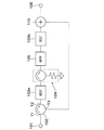
図1は本発明に係るフィルタ回路の第1の実施例を示すブロック図である。 FIG. 1 is a block diagram showing a first embodiment of a filter circuit according to the present invention.
このフィルタ回路においては、入力端子101と出力端子106との間に、サーキュレータ102と、帯域阻止フィルタ(BSF:Band Stop Filter)103aと、アイソレータ104と、帯域通過フィルタ(BPF:Band Pass Filter)105と、帯域阻止フィルタ103bと、合成回路110とが縦列接続されている。サーキュレータ102は端子T1、T2、T3を有する。端子T1は入力端子101に接続され、端子T2は帯域阻止フィルタ103aの入力に接続されている。合成回路110の入力には、サーキュレータ102の端子T3と、帯域阻止フィルタ103bの出力とが接続されている。合成回路110の出力は出力端子106に接続されている。
In this filter circuit, between an
サーキュレータ102は、入力端子101から端子T1に入力される信号を端子T2から出力して、帯域阻止フィルタ(BSF:Band Stop Filter)103aに伝達する。またサーキュレータ102は、帯域阻止フィルタ103aで反射させられた信号を端子T2において受け取り、端子T3から出力して合成回路110に伝達する。またサーキュレータ102は端子T3で受け取る信号を、端子T1から出力して入力端子101に伝達する。
The
帯域阻止フィルタ(BSF:Band Stop Filter)103aは、耐電力量Wbsf (W)を有し、阻止帯域として、反射特性の3dB帯域幅を決める2点の周波数fbsf1、fbsf2(fbsf1<fbsf2)をもつ。帯域阻止フィルタ103aの阻止帯域は、本フィルタ回路の中心周波数を含んでいる。また帯域阻止フィルタ103aの阻止帯域は、入力端子101に入力される信号の中心周波数を含んでいる。帯域阻止フィルタ103aは、阻止帯域内の信号を反射させ、阻止帯域外の帯域の信号を通過させる。
A band stop filter (BSF) 103a has a power handling capability Wbsf (W), and has two frequencies fbsf1 and fbsf2 (fbsf1 <fbsf2) that determine a 3 dB bandwidth of reflection characteristics as a stop band. The stop band of the
アイソレータ104は、帯域阻止フィルタ103aを通過した信号をそのまま帯域通過フィルタ(BPF:Band Pass Filter)105に伝達する。またアイソレータ104は、帯域通過フィルタ105で反射させられた信号(通過帯域外の信号)を減衰させて(吸収して)帯域阻止フィルタ103aに戻ることを阻止する。
The
帯域通過フィルタ(BPF:Band Pass Filter)105は、耐電力量Wbpf (W)を有し、通過帯域として、通過特性の3dB帯域幅を決める2点の周波数fbpf1、fbpf2(fbpf1<fbpf2)をもつ。帯域通過フィルタ105は、通過帯域内の信号を通過させ、通過帯域外の信号を反射させる。
A band pass filter (BPF: Band Pass Filter) 105 has a power handling capability Wbpf (W), and has two frequencies fbpf1 and fbpf2 (fbpf1 <fbpf2) that determine the 3 dB bandwidth of the pass characteristic as the passband. The
ここで帯域阻止フィルタ103aの耐電力量Wbsfと、帯域通過フィルタ105の耐電力量Wbpfとの間には、Wbsf>Wbpfの関係がある。つまり帯域阻止フィルタ103aの耐電力量Wbsfは、帯域通過フィルタ105の耐電力量Wbpfよりも大きい。
Here, there is a relationship of Wbsf> Wbpf between the power handling capability Wbsf of the
また、帯域阻止フィルタ103aの反射特性の3dB帯域幅を決める2点の周波数fbsf1、fbsf2(fbsf1<fbsf2)と、帯域通過フィルタ105の通過特性の3dB帯域幅を決める2点の周波数fbpf1、fbpf2(fbpf1<fbpf2)との間には、fbpf1<fbsf1<fbsf2<fbpf2の関係がある。つまり、帯域通過フィルタの通過帯域は、帯域阻止フィルタの阻止帯域を包含する関係にある。
Further, two frequencies fbsf1 and fbsf2 (fbsf1 <fbsf2) that determine the 3 dB bandwidth of the reflection characteristic of the
帯域阻止フィルタ103bは、上記帯域阻止フィルタ103aと同一の阻止帯域を有する。帯域阻止フィルタ103bは、実際の無線装置を考えた場合に、アンテナの状況に応じてアンテナから放射されない電力が戻ってきた場合に帯域通過フィルタ105への電力流入を避けるためのものである。つまり、帯域阻止フィルタ103bは、アンテナから反射により戻ってきた信号に含まれる、帯域阻止フィルタ103bの阻止帯域の大電力信号を反射させることで、該大電力信号が帯域通過フィルタ105に入力されて帯域通過フィルタ105が破壊されるのを阻止する。
The
合成回路110は、帯域阻止フィルタ103aで反射しサーキュレータ102の端子T3を介して入力される信号(帯域阻止フィルタ103aの阻止帯域の信号)と、帯域通過フィルタ105から出力され帯域阻止フィルタ103bを経由した信号(帯域通過フィルタ105の通過帯域の信号)とを合成して合成信号を取得し、取得した合成信号を出力端子106から出力する。つまり、入力端子101から入力され帯域阻止フィルタ103aと帯域通過フィルタ105と帯域阻止フィルタ103bとを通過した信号と、帯域阻止フィルタ103aで反射させられサーキュレータ102で取り出された信号とが合成回路110で合成されて、出力端子106から出力される。
The
以上の構成により、帯域阻止フィルタ103aよりも耐電力量の小さな帯域通過フィルタ105を用いても耐電力性を損なうことなく急峻なスカート特性をもつフィルタ回路を構成できる。これはたとえば単位面積当たりに超伝導状態で流せる電流値に限界値を持つ超伝導体により帯域通過フィルタを構成する場合に有効である。従来技術のフィルタ構成では臨界電流値を越えてしまうために大きな電力を通過(フィルタ)させられない問題点があったが、本実施例では、帯域阻止フィルタ103aの阻止帯域内に大きな電力密度を持つ信号のうち、阻止帯域の信号を帯域阻止フィルタで反射させ、阻止帯域外の信号電力の小さな信号のみを超伝導フィルタ(帯域通過フィルタ)に通し、超伝導フィルタを通過した信号と、上記阻止帯域の信号とを合成する。このようにして大きな耐電力性と急峻なスカート特性を持つフィルタ回路を実現することができる。
With the above configuration, a filter circuit having a steep skirt characteristic can be configured without impairing the power durability even when the band-
図1の合成回路110としてサーキュレータ115を用いた場合の例を図2に示す。サーキュレータ102からサーキュレータ115に入力される信号を帯域阻止フィルタ103b側に伝達させ、帯域阻止フィルタ103bにおいて反射させる。反射させられた信号は、帯域通過フィルタ105の出力信号とあわせて出力端子106から出力される。アンテナからの反射電力はサーキュレータ115によってサーキュレータ102の端子T3に伝達され、サーキュレータ102の端子T1から入力端子101に伝達される。したがってアンテナからの反射電力が、耐電力の低い帯域通過フィルタ105を通ることにより帯域通過フィルタ105が破壊されることない。
An example in which the
図3は本発明に係るフィルタ回路の第2の実施例を示すブロック図である。 FIG. 3 is a block diagram showing a second embodiment of the filter circuit according to the present invention.
図3のフィルタ回路では、図2の帯域通過フィルタ105の代わりに、共振器群回路112が配置されている。
In the filter circuit of FIG. 3, a
共振器群回路112は、アイソレータ104を通過した信号を分割する電力分配部(電力分割部)210と、電力分配部210に並列に接続され電力分配部210によって分割された各信号が与えられるブロック111(1)、111(2)・・・と、各ブロックを通過した信号を合成する電力合成部211と、を有する。各ブロック111(N)(N=1、2、・・・)は、超伝導体(SC)により構成された耐電力量Wreso (W)以下の共振器107(N)と、共振器107(N)に縦列接続された遅延回路(位相調整手段)108(N)とを有する。各共振器107(N)の共振周波数freso-i(iは1以上N以下)は互いに異なる。各遅延回路108(N)は、電力合成部211における電力合成時に、隣り合う共振周波数をもつ信号同士が180+360×k±30度(kは0以上の整数)の範囲の位相差(逆相)条件を満たすようにすることで、隣り合う共振周波数をもつ信号同士の和合成を得る。和合成について図5および図6を用いて簡単に説明する。図5(A)のように共振器並列接続型において、共振周波数f1、f2をもつ2つの共振器を通過した信号を合成する際、これらの信号を180度の遅延差をもたせて合成すると、図5(B)のように、得られる信号301aは、2つの信号(共振波形)302a、302bの和合成となる。外部回路結合係数Jqeを調整することで帯域通過フィルタを構成できる。
一方、図6(A)のように、共振周波数f1、f2をもつ2つの共振器を通過した信号を遅延差0度で合成すると、図6(B)のように、得られる信号301bは、2つの信号(共振波形)302a、302bの差合成となる。したがって、図3のフィルタ回路では、和合成が得られるように、隣接するブロック間を通過する信号に、180度の遅延差を持たせるようにしている。ここで遅延回路108(N)の数値(0deg,180deg)は一例であり他の値を用いることもできる。また共振器107(N)と遅延回路108(N)の順番はブロックごとに入れ替えても同様の特性を得ることができる。
The
On the other hand, as shown in FIG. 6A, when signals that have passed through the two resonators having the resonance frequencies f1 and f2 are combined with a delay difference of 0 degree, as shown in FIG. This is a difference synthesis of the two signals (resonance waveforms) 302a and 302b. Therefore, in the filter circuit of FIG. 3, a signal that passes between adjacent blocks has a delay difference of 180 degrees so that sum synthesis can be obtained. Here, the numerical value (0 deg, 180 deg) of the delay circuit 108 (N) is an example, and other values may be used. The same characteristics can be obtained even if the order of the resonator 107 (N) and the delay circuit 108 (N) is changed for each block.
帯域阻止フィルタ103aの耐電力量Wbsfと、各共振器107(N)の耐電力量Wresoとの間にはWbsf>Wresoの関係がある。また、帯域阻止フィルタ103aの反射特性の3dB帯域幅を決める2点の周波数fbsf1、fbsf2(fbsf1<fbsf2)と、各共振器の共振周波数freso-i(iは1以上N以下)との間には、freso-i<fbsf1もしくはfbsf2<freso-iの関係がある。すなわち、各共振器は、帯域阻止フィルタ103aの阻止帯域外に共振周波数を有し、共振器群回路112は、このような各共振器と、電力分配部210と、電力合成部211とを用いることにより、帯域阻止フィルタ103aの阻止帯域外の信号から所望帯域の信号を抽出する。
There is a relationship of Wbsf> Wreso between the power handling capability Wbsf of the
以上の構成により、図2の帯域通過フィルタ105に用いる共振器の数よりも少ない数の共振器数で急峻なフィルタ特性と耐電力性とをあわせもつフィルタ回路を構成できる。すなわち図2の帯域通過フィルタ105はたとえば図26または図27に示したように共振器の縦列接続または並列接続により構成できるが、図3では帯域域阻止フィルタ103aの阻止帯域内に共振周波数をもつ共振器を用いる必要はないため、その分、共振器の数を少なくできる。
With the above configuration, a filter circuit having both steep filter characteristics and power durability can be configured with a smaller number of resonators than the number of resonators used in the
図4は、図3のフィルタ回路において共振器群回路112の構成を変更したものである。ブロック111(N)において、3つの結合回路11(N)〜13(N)にはさまれた2つの共振器107(N)と、遅延回路108(N)が縦列接続されている。結合回路12(N)は、共振器間結合係数Mj(jは1〜N)により2つの共振器107(N)と結合され、各共振器107(N)は、フィルタ回路の中心周波数f0と同じ共振周波数を持つ。M1<M2<…<MNの関係がある。結合回路11(N)は電力分配部210と1つの共振器107(N)とを外部回路結合係数(外部Q)Jqej(jは1〜N)で結合し、結合回路13(N)はもう1つの共振器107(N)と遅延回路108(N)とを、外部回路結合係数Jqej(jは1〜N)で結合する。Jqe1>Jqe2>…>JqeN(外部Qで記述した場合;Qe1<Qe2<…<QeN)の関係がある。遅延回路108(N)は、2つの共振器107(N)間結合により縮退のとけた信号が、隣接するブロック間(Mが隣合うブロック間)で180+360×k±30度(kは0以上の整数)の範囲の位相差(逆相)条件を満たすようにすることで、隣接するブロック間で、信号の和合成を得られるようにする。共振器群の中のブロックの順番を入れ替えても同様にフィルタを構成できる。また、2つの共振器群の中のブロックの順番も同じでなくても同様にフィルタを構成できる。
FIG. 4 shows a modification of the configuration of the
このフィルタ回路では、帯域阻止フィルタ103aの耐電力量Wbsf>各共振器の耐電力量Wresoの関係がある。また、帯域阻止フィルタ103aの反射特性の3dB帯域幅を決める2点の周波数の差fbsf2-fbsf1<共振器間結合係数Mj×中心周波数f0の関係がある。なお帯域阻止フィルタ103a、103bに含まれる共振器数は偶数個である(後述する図20参照)。
In this filter circuit, there is a relationship of the power tolerance Wbsf of the
図7は本発明に係るフィルタ回路の第3の実施例を示すものである。 FIG. 7 shows a third embodiment of the filter circuit according to the present invention.
図3のフィルタ回路において、サーキュレータの代わりに4開口素子(4端子素子)を用いる場合のフィルタ回路の実施例が示されている。次式で定義されるSパラメータをもつ4開口素子の各端子を端子1〜端子4として定義する。

4開口素子の例としては、図8に示す導波管を用いたマジックTなどがある。マジックTに付した各番号と、図7の4開口素子202、207の各端子との対応関係は図9に示したとおりとなっている。また、伝送線路(マイクロストリップ線路)を用いた4開口素子の例としては図10に示すようなラットレース回路がある。一般的に4開口素子はサーキュレータに比べて低損失な特性を持っており、フィルタ回路を通過する損失を減らすためには4開口素子を用いる方法が有効である。図7の例では、4開口素子202の端子3は端子A、端子1は端子B、端子2は端子C、端子4は端子Dに相当し、4開口素子207の端子4は端子E、端子1は端子F、端子2は端子G、端子3は端子Hに相当する。
As an example of the 4-aperture element, there is a magic T using a waveguide shown in FIG. The correspondence between the numbers assigned to the magic T and the respective terminals of the four-opening
4開口素子202の端子3に入力端子201が接続され、4開口素子202の端子4と4開口素子207の端子4とが接続され、4開口素子207の端子3は出力端子209に接続される。4開口素子202の端子1と4開口素子207の端子1との間には、遅延回路203Aと帯域阻止フィルタ204Aと共振器群回路112Aと遅延回路203Bと帯域阻止フィルタ204Bとが縦列接続される。4開口素子202の端子2と4開口素子207の端子2との間には、帯域阻止フィルタ204Cと遅延回路203Cと共振器群回路112Bと帯域阻止フィルタ204Dと遅延回路203Dとが縦列接続される。共振器群回路112A、112Bの構成は同一であり、各々において、異なる周波数の単一共振器をもつブロックが並列接続されている。4つの帯域阻止フィルタ204A〜204Dはそれぞれ同一の阻止帯域を有している。
The
遅延回路203Aは、4開口素子202の端子1から帯域阻止フィルタ204Aまでの電気長と、4開口素子202の端子2から帯域阻止フィルタ204Cまでの電気長との差(位相差)を90度とする。遅延回路203Aは、端子1から送出され帯域阻止フィルタ204Aで反射して4開口素子202の端子1に戻される信号を該端子1から送出された信号に対して逆相にし、また、帯域阻止フィルタ204Aを通過し共振器群回路112Aで反射して該端子1に戻される信号を、該端子1から送出された信号に対して逆相にする。
The
遅延回路203Dは、4開口素子207の端子1から帯域阻止フィルタ204Bまでの電気長と、4開口素子207の端子2から帯域阻止フィルタ204Dまでの電気長との差(位相差)を90度とする。遅延回路203Dは、該端子2から送出され帯域阻止フィルタ204Dで反射して4開口素子207の端子2に戻される信号を該端子2から送出された信号に対して逆相にし、また該端子2から送出され帯域阻止フィルタ204Dを通過し共振器群回路112Bで反射して該端子2に戻される信号を、該端子2から送出された信号に対して逆相にする。
The
遅延回路203Cは、4開口素子202の端子1および端子2から共振器群回路112A、112Bまでの電気長の差(位相差)を0度とする。遅延回路203Cは、該端子2から送出され帯域阻止フィルタ204Cを通過し共振器群回路112Bで反射して4開口素子202の端子2に戻される信号を、該端子2から送出された信号に対して逆相にする。
The
遅延回路203Bは、4開口素子207の端子1および端子2から共振器群回路112A、112Bまでの電気長の差(位相差)を0度とする。遅延回路203Bは、遅延回路203Cの配置による位相遅延を補完するために配置され、遅延回路203Cと同一の位相遅延量を有する。
The
図7のフィルタ回路の具体例を図11に示す。共振器群回路112A、112B内の2つの共振器402(1)、402(2)と、遅延回路(伝送線路)403は超伝導により形成されている。共振器402(1)、402(2)の共振周波数fL1,fU1(fL1<fU1)は帯域阻止フィルタ(401、404)の阻止帯域を挟んでそれぞれ両側に位置する(すなわちfL1,fU1は隣接しない)。図中に示される波形は、入力端子201への入力信号としてフラットな信号を入力した場合に矢印によって示される代表的な箇所での通過スペクトルを示す。以下本フィルタ回路の動作について説明する。
A specific example of the filter circuit of FIG. 7 is shown in FIG.
入力端子201から入力された信号は4開口素子202で電力が2分配されて端子1及び端子2から逆相出力される。端子1から出力された信号は、共振器401Aと結合回路404Aから成る1段の帯域阻止フィルタ204Aにおいて中心周波数fc1近傍の信号(阻止帯域の信号)が反射させられる。同様に、端子2から出力された信号は、共振器401Cと結合回路404Cから成る1段の帯域阻止フィルタ204Cにおいて中心周波数fc1近傍の信号(阻止帯域の信号)が反射させられる。帯域阻止フィルタ204A、204Cで反射させられた信号は遅延回路203Aにより同位相の関係とされて4開口素子202Aの端子1および端子2に戻り、これらの信号が電力合成されて端子4から出力される。
The signal input from the
4開口素子202Aの端子4から出力された信号は4開口素子207の端子4へ入力され、入力された信号は2分配されて端子1及び端子2から同相の関係で出力される。端子1から出力された信号は1つの共振器401Bと結合回路404Bから成る1段の帯域阻止フィルタ204Bで中心周波数fc1近傍の信号(阻止帯域の信号)が反射させられる。同様に、端子2から出力された信号も1つの共振器401Dと結合回路404Dから成る1段の帯域阻止フィルタ204Dで中心周波数fc1近傍の信号(阻止帯域の信号)が反射させられる。帯域阻止フィルタ204B、204Dで反射させられた信号は、遅延回路203Dによって逆位相の関係とされて、4開口素子207の端子1および端子2に戻る。4開口素子207は、端子1および端子2に入力された阻止帯域の信号を合成して端子3から出力する。
The signal output from the
一方、帯域阻止フィルタ204Aを通過した周波数帯の信号(阻止帯域外の信号)は共振器群回路112Aに入力され、共振器群回路112Aにおいて各共振器402(1)、402(2)による共振波形の信号が抽出され、抽出された各共振波形の信号を合成した合成波信号(所望帯域の信号)が通過する。帯域阻止フィルタ204Cを通過した周波数帯の信号(阻止帯域外の信号)は遅延回路403Cを経由して共振器群回路112Bに入力され、共振器群回路112Bおいて各共振器402(1)、402(2)による共振波形の信号が抽出され、抽出された各共振波形の信号を合成した合成波信号(所望帯域の信号)が通過する。共振器群回路112A、を通過した信号は遅延回路403Bを経由し、共振器群回路112Bを通過した信号と同相で4開口素子B207の端子1及び端子2に入力される。4開口素子207は、端子1および端子2に入力された所望帯域の信号を合成して端子3から出力する。
On the other hand, the signal in the frequency band that passes through the
共振器群回路112A、112Bを通過しない信号(反射した信号)は、遅延回路203Aおよび403Cにより逆位相の関係で4開口素子202の端子1および端子2に戻り、電力合成されて端子3から、入力端子201に戻される。
The signals (reflected signals) that do not pass through the
以上のように、フィルタ回路の中心周波数付近fc1の大きな電力は超伝導の共振器群回路112A、112Bを通過しないことから、超伝導体を用いた急峻なフィルタ特性と高い耐電力性とを持つフィルタ特性の両立を行うことができる。
As described above, a large power of the center frequency around f c1 of the filter circuit
一例として、図11のフィルタ回路への入力信号として図12(A)のスペクトルをもつ信号を入力した場合の周波数応答を図12(B)に示しておく。 As an example, FIG. 12B shows a frequency response when a signal having the spectrum of FIG. 12A is input as an input signal to the filter circuit of FIG.
図13は4開口素子207の端子3および4端子の接続先を逆にした場合の例を示す。すなわち端子3が4開口素子202の端子4に接続され、端子4が出力端子209に接続されている。これにより遅延回路403Cの遅延量を図11の270度から90度に減らすことができ(180度の遅延位相回路を省略でき)、回路構成を縮小できる。すなわち、4開口素子207の端子1および端子2への入力信号を同相にするため、図11の遅延回路403Cの遅延量を180度減らすことができる。図13では4開口素子207の端子3および4端子の接続先を逆にする例を示したが、4開口素子202の端子3および端子4の接続先を逆にしてもよく、あるいは4開口素子202、207の両方の端子3および端子4の接続先を逆にしてもよい。
FIG. 13 shows an example where the connection destinations of the
図14は、4開口素子202と4開口素子207とを接続する線路に180度の遅延回路212を入れた例を示す。これにより、図11の共振器群回路112A、112Bに含まれていた遅延回路403B、403Cの遅延量をそれぞれ270度から90度に減少できるため、フィルタ回路全体の線路長を短くして、回路規模を縮小できる。
FIG. 14 shows an example in which a
図15は、共振器群回路112A、112B内に、超伝導体により形成した共振器402(1)〜402(4)を4つ並列に配置した場合の例を示す。共振器402(1)、402(2)の共振周波数fL2,fL1(fL2<fL1)は、帯域阻止フィルタ204Aの阻止帯域外の帯域のうち低域側に含まれる。各共振器402(1)、402(2)を通過した信号は、和合成を得るため遅延回路403Aによって180度の位相差をもたせられる。共振器402(3)、402(4)の共振周波数fU1,fU2(fU1<fU2)は、帯域阻止フィルタ204Aの阻止帯域外の帯域のうち高域側に含まれる。各共振器402(3)、402(4)を通過した信号は、和合成を得るため遅延回路403Bによって180度の位相差をもたせられる。図16にこのフィルタ回路の周波数応答を示す。図11のフィルタ回路の周波数応答を示す図12(B)と比較して分かるように、多くの共振器を用いることで、より急峻な出力信号301を得ることができる。
Figure 15 is a
図17は、図15のフィルタ回路において、帯域阻止フィルタを2つの共振器を用いて構成した例を示す。たとえば帯域阻止フィルタ204Aは、2つの共振器401Aと、2つの結合回路404Aと、遅延回路203A’とにより構成される。他の帯域阻止フィルタ204B〜204Cも同様である。
FIG. 17 shows an example in which the band rejection filter is configured using two resonators in the filter circuit of FIG. For example, the
図18は本発明に係るフィルタ回路の第4の実施例を示すものである。 FIG. 18 shows a fourth embodiment of the filter circuit according to the present invention.
このフィルタ回路は、図7のフィルタ回路の共振器群回路112A、112Bを、図4の共振器群回路112に置換したものである。ただし、共振器群回路112Bでは遅延回路403A、403Bの位置が、電力合成部211の直前ではなく、電力分配部210の直後に置かれている。なお、帯域阻止フィルタ204A〜204Dにおける共振器の数は偶数個である。図18のフィルタ回路の周波数応答を図19に示す。縮退が解けた各共振波形302の重ね合わせを利用してフィルタ特性301を実現している。また、共振器間結合係数Mjが大きくなるほど縮退のとけた周波数差(各共振波形302のピーク幅)は大きくなる。ここでM1=(fU1-fL1)/f0,M2=(fU2-fL2)/f0の関係がある。帯域阻止フィルタを2つの共振器を用いて構成し、共振器群回路112A、112Bにおける、超伝導共振器の縦列接続を含むブロック数が1つの場合のフィルタ回路の例を図20に示しておく。このように超伝導共振器の縦列接続を含むブロックの数は1つのみでもよい。
This filter circuit is obtained by replacing the
図21は、図7のフィルタ回路において、遅延回路203Bと帯域阻止フィルタ204Bとの位置関係を逆にし、また遅延回路203Dと帯域阻止フィルタ204Dとの位置関係を逆にした例を示す。このように遅延回路と帯域阻止フィルタとの位置関係が逆であっても図7の構成と同様の効果を得ることが可能である。
FIG. 21 shows an example in which the positional relationship between the
図22は、図7のフィルタ回路において、4開口素子202の端子4と、4開口素子207の端子4との間に、低域通過フィルタ(Low Pass Filter)213を挿入した例を示す。この低域通過フィルタ213により、帯域阻止フィルタ204A、204Bで反射させられた、阻止帯域外の高調波信号の通過を阻止して、フィルタ特性の改善を図ることができる。低域通過フィルタの代わりに、特定周波数を減衰させるための帯域阻止フィルタ、または低周波側のリークを無くすための高域通過フィルタなども挿入してもよい。
FIG. 22 shows an example in which a
図23は、図11のフィルタ回路の動作を確認するためシミュレーションを行った回路の例を示す。計算に用いたパラメータはfC1=5.26 GHz、fL1=5.2551 GHz、fU1=5.2649 GHz、Jbsfの結合係数は0.036、Jqeの外部Qは1600として計算した。計算結果を図24に示す。結合回路はキャパシタンスのπ型回路を用い、共振器402としては180度の伝送線路を、帯域阻止フィルタ204の共振器には90度の伝送線路をそれぞれ用いている。
FIG. 23 shows an example of a circuit that is simulated to confirm the operation of the filter circuit of FIG. The parameters used in the calculation are f C1 = 5.26 GHz, f L1 = 5.2551 GHz, f U1 = 5.2649 GHz, the coupling coefficient of J bsf is 0.036, and the external Q of J qe is 1600. The calculation results are shown in FIG. The coupling circuit uses a π-type circuit of capacitance, a 180-degree transmission line is used as the
図25は、これまでに述べてきたフィルタ回路を無線通信装置に組み込んだ例を示す。無線通信装置の送信部が概略的に示されている。送信すべきデータ500は信号処理回路501に入力され、ディジタル−アナログ変換、符号化及び変調などの処理が施されることにより、ベースバンドあるいは中間周波数 (Intermediate Frequency;IF)帯の送信信号が生成される。信号処理回路501により生成された送信信号は周波数変換器(ミキサ)502に入力され、ローカル信号発生器503からのローカル信号と乗算されることによって、無線周波数 (Radio Frequency;RF)帯の信号に周波数変換、すなわちアップコンバートされる。ミキサ502から出力されるRF信号は電力増幅器504によって増幅された後、本実施形態に係わる帯域制限フィルタ(送信フィルタ)回路505に入力され、このフィルタ回路505で帯域制限を受けて不要な周波数成分が除去された後、アンテナ506から電波として空間に放射される。
FIG. 25 shows an example in which the filter circuit described so far is incorporated in a wireless communication apparatus. A transmission unit of a wireless communication device is schematically shown. Data 500 to be transmitted is input to a
101…入力端子
102…サーキュレータ
103a、103b…帯域阻止フィルタ
104…アイソレータ
105…帯域通過フィルタ
106…出力端子
107(1)〜107(N)…共振器
108(1)〜108(N)…遅延回路(位相調整手段、伝送線路)
110…合成回路
111(1)〜111(N)…ブロック
112、112A、112B…共振器群回路
205(1)〜205(N)…共振器
206(1)〜206(N)…遅延回路(位相調整手段、伝送線路)
201…入力端子
202…4開口素子
203…遅延回路(位相調整手段、伝送線路)
204A〜204D…帯域阻止フィルタ
207…4開口素子
209…出力端子
210…電力分配部(電力分割部)
211…電力合成部
212…遅延回路
213…低域通過フィルタ
401A〜401D…帯域阻止フィルタ用共振器
402…超伝導共振器
403B〜403C…遅延回路(位相調整手段、超伝導伝送線路)
404A〜404D…帯域阻止フィルタ用結合回路
405(1)、405(2)…超伝導共振器用結合回路
500…データ
501…信号処理回路
502…周波数変換器
503…ローカル信号発生器
504…電力増幅器
505…帯域制限フィルタ
506…アンテナ
DESCRIPTION OF
110... Synthetic circuits 111 (1) to 111 (N)...
201 ...
204A to 204D,
211 ...
404a-404d ... band-stop filter for coupling circuit 405 (1), 405 (2) ... superconductive resonator coupling circuits 500 ...
Claims (14)
前記信号の中心周波数を阻止帯域内に有し、前記信号に含まれる前記阻止帯域内の信号を反射させ前記阻止帯域外の信号を通過させる帯域阻止フィルタと、
前記阻止帯域を包含する通過帯域を有し、前記帯域阻止フィルタを通過した信号のうち前記通過帯域内の信号を通過させる帯域通過フィルタと、
前記帯域阻止フィルタで反射した信号と、前記帯域通過フィルタを通過した信号とを合成して合成信号を得る合成回路と、
前記合成信号を出力する出力端子と、
を備えたフィルタ回路。 An input terminal for inputting a signal;
A band stop filter having a center frequency of the signal in a stop band, reflecting a signal in the stop band included in the signal and passing a signal outside the stop band;
A bandpass filter that has a passband that includes the stopband, and that passes signals within the passband among signals that have passed through the bandstop filter;
A combining circuit that combines a signal reflected by the band rejection filter and a signal that has passed through the band pass filter to obtain a combined signal;
An output terminal for outputting the combined signal;
Filter circuit with
前記合成回路は第2のサーキュレータとして構成され、前記第1のサーキュレータから伝達された信号を前記第2の帯域阻止フィルタに戻し、前記第2の帯域阻止フィルタで反射した信号と、前記帯域通過フィルタから前記第2の帯域阻止フィルタを経由してきた信号とを前記出力端子に伝達する、
ことを特徴とする請求項2に記載のフィルタ回路。 A second band rejection filter disposed between the band pass filter and the synthesis circuit and having the same stop band as the band rejection filter;
The synthesizing circuit is configured as a second circulator, a signal transmitted from the first circulator is returned to the second band rejection filter, a signal reflected by the second band rejection filter, and the band pass filter A signal transmitted from the second band rejection filter to the output terminal,
The filter circuit according to claim 2.
前記信号の中心周波数を含む阻止帯域を有し、前記信号に含まれる前記阻止帯域内の信号を反射させ前記阻止帯域外の信号を通過させる帯域阻止フィルタと、
複数の共振器を用いて前記帯域阻止フィルタを通過した信号から所望帯域の信号を通過させる共振器群回路と、
前記共振器群回路を通過した信号と、前記帯域阻止フィルタで反射した信号とを合成して合成信号を得る合成回路と、
前記合成信号を出力する出力端子と、
を備えたフィルタ回路。 An input terminal for inputting a signal;
A band stop filter having a stop band including a center frequency of the signal, reflecting a signal in the stop band included in the signal and passing a signal outside the stop band;
A resonator group circuit that passes a signal in a desired band from a signal that has passed through the band rejection filter using a plurality of resonators;
A combining circuit that combines a signal that has passed through the resonator group circuit and a signal that has been reflected by the band rejection filter to obtain a combined signal;
An output terminal for outputting the combined signal;
Filter circuit with
前記合成回路は第2のサーキュレータとして構成され、前記第1のサーキュレータから伝達されてきた信号を前記第2の帯域阻止フィルタに戻し、前記第2の帯域阻止フィルタで反射した信号と、前記共振器群回路から前記第2の帯域阻止フィルタを経由してきた信号とを前記出力端子に送る、
ことを特徴とする請求項7に記載のフィルタ回路。 A second band-stop filter disposed between the resonator group circuit and the synthesis circuit and having the same stop band as the band-stop filter;
The synthesizing circuit is configured as a second circulator, a signal transmitted from the first circulator is returned to the second band rejection filter, a signal reflected by the second band rejection filter, and the resonator A signal sent from a group circuit via the second band rejection filter to the output terminal;
The filter circuit according to claim 7.
前記入力端子から入力された信号を端子Aで受け取り受け取った信号を分割して端子Bおよび端子Cから送出し、また、前記端子Bおよび端子Cに与えられた信号を合成して端子Dから送出する、第1の4端子素子と、
前記入力端子から入力された信号の中心周波数を阻止帯域内に有し、前記端子Bから送出された信号に含まれる前記阻止帯域内の信号を前記端子Bに反射させ阻止帯域外の信号を通過させる第1帯域阻止フィルタと、
前記第1帯域阻止フィルタの阻止帯域と同一の阻止帯域を有し、前記端子Cから送出された信号に含まれる前記阻止帯域内の信号を前記端子Cに反射させ前記阻止帯域外の信号を通過させる第2帯域阻止フィルタと、
第1の複数の共振器を用いて前記第1帯域阻止フィルタを通過した信号から所望帯域の信号を通過させる第1共振器群回路と、
前記第1の複数の共振器の各々と同じ共振周波数を有する第2の複数の共振器を用いて前記第2帯域阻止フィルタを通過した信号から前記所望帯域の信号を通過させる第2共振器群回路と、
前記端子Dから送出された信号を端子Eにおいて受け取り受け取った信号を分割して端子Fおよび端子Gから送出し、また、前記端子Fおよび端子Gに与えられた信号を合成して端子Hから送出する、第2の4端子素子と、
前記第1帯域阻止フィルタと同一の阻止帯域を有し、前記第1共振器群回路を通過した信号を前記端子Fへ通過させ、前記端子Fから送出された信号を前記端子Fに反射させる第3帯域阻止フィルタと、
前記第1帯域阻止フィルタと同一の阻止帯域を有し、前記第2共振器群回路を通過した信号を前記端子Gへ通過させ、前記端子Gから送出された信号を前記端子Gに反射させる第4帯域阻止フィルタと、
前記端子Hから送出された信号を出力する出力端子と、
を備えたフィルタ回路。 An input terminal for inputting a signal;
The signal inputted from the input terminal is received at the terminal A, and the received signal is divided and sent out from the terminal B and the terminal C. The signals given to the terminals B and C are synthesized and sent out from the terminal D. A first four-terminal element;
The center frequency of the signal input from the input terminal is in the stop band, and the signal in the stop band included in the signal transmitted from the terminal B is reflected to the terminal B and passes the signal outside the stop band. A first band rejection filter to be
The stop band is the same as the stop band of the first band stop filter, and the signal within the stop band included in the signal transmitted from the terminal C is reflected to the terminal C and the signal outside the stop band is passed. A second band rejection filter for causing
A first resonator group circuit that passes a signal in a desired band from a signal that has passed through the first band rejection filter using a first plurality of resonators;
A second resonator group that passes a signal in the desired band from a signal that has passed through the second band rejection filter using a plurality of second resonators having the same resonance frequency as each of the first plurality of resonators; Circuit,
The signal sent from the terminal D is received at the terminal E, the received signal is divided and sent from the terminal F and the terminal G, and the signals given to the terminals F and G are synthesized and sent from the terminal H. A second four-terminal element;
A first band-pass filter that has the same stopband as the first band-stop filter, passes a signal that has passed through the first resonator group circuit to the terminal F, and reflects a signal transmitted from the terminal F to the terminal F; A three-band rejection filter;
A first passband having the same stopband as the first bandstop filter, passing a signal that has passed through the second resonator group circuit to the terminal G, and reflecting a signal transmitted from the terminal G to the terminal G. A 4-band rejection filter;
An output terminal for outputting a signal transmitted from the terminal H;
Filter circuit with
前記送信信号を増幅する電力増幅器と、
増幅された送信信号をフィルタ処理する請求項1ないし13のいずれか一項に記載のフィルタ回路と、
前記フィルタ回路から得られる信号を空間に電波として放射するアンテナと、
を備えた無線通信装置。 A signal processing circuit that performs transmission processing on transmission data to obtain a transmission signal;
A power amplifier for amplifying the transmission signal;
A filter circuit according to any one of claims 1 to 13, which filters the amplified transmission signal;
An antenna that radiates a signal obtained from the filter circuit as a radio wave in space;
A wireless communication device comprising:
Priority Applications (2)
| Application Number | Priority Date | Filing Date | Title |
|---|---|---|---|
| JP2006332415A JP4264101B2 (en) | 2006-12-08 | 2006-12-08 | Filter circuit and wireless communication device |
| US11/856,321 US8005451B2 (en) | 2006-12-08 | 2007-09-17 | Filter circuit and radio communication apparatus |
Applications Claiming Priority (1)
| Application Number | Priority Date | Filing Date | Title |
|---|---|---|---|
| JP2006332415A JP4264101B2 (en) | 2006-12-08 | 2006-12-08 | Filter circuit and wireless communication device |
Publications (2)
| Publication Number | Publication Date |
|---|---|
| JP2008147959A JP2008147959A (en) | 2008-06-26 |
| JP4264101B2 true JP4264101B2 (en) | 2009-05-13 |
Family
ID=39498686
Family Applications (1)
| Application Number | Title | Priority Date | Filing Date |
|---|---|---|---|
| JP2006332415A Active JP4264101B2 (en) | 2006-12-08 | 2006-12-08 | Filter circuit and wireless communication device |
Country Status (2)
| Country | Link |
|---|---|
| US (1) | US8005451B2 (en) |
| JP (1) | JP4264101B2 (en) |
Cited By (1)
| Publication number | Priority date | Publication date | Assignee | Title |
|---|---|---|---|---|
| US7945300B2 (en) | 2007-08-28 | 2011-05-17 | Kabushiki Kaisha Toshiba | Plural channel superconducting filter circuit having release of resonance frequency degeneracy and usable in radio frequency equipment |
Families Citing this family (8)
| Publication number | Priority date | Publication date | Assignee | Title |
|---|---|---|---|---|
| JP4264101B2 (en) | 2006-12-08 | 2009-05-13 | 株式会社東芝 | Filter circuit and wireless communication device |
| JP4679618B2 (en) * | 2008-09-11 | 2011-04-27 | 株式会社東芝 | Filter circuit and wireless communication device |
| KR101083531B1 (en) * | 2009-09-01 | 2011-11-18 | 에스케이 텔레콤주식회사 | Method and coupling apparatus for dividing receiving and transmitting signal |
| WO2011033573A1 (en) | 2009-09-18 | 2011-03-24 | 株式会社 東芝 | High-frequency filter |
| JP2012222725A (en) * | 2011-04-13 | 2012-11-12 | Toshiba Corp | Active array antenna device |
| JP5846019B2 (en) * | 2012-03-30 | 2016-01-20 | 富士通株式会社 | Wireless device |
| EP2733781A1 (en) * | 2012-11-16 | 2014-05-21 | Alcatel-Lucent | A filter assembly and a method of filtering |
| RU2766057C1 (en) * | 2021-03-01 | 2022-02-07 | Станислав Константинович Крылов | Device for increasing amplitude frequency response of microwave filter unit |
Family Cites Families (28)
| Publication number | Priority date | Publication date | Assignee | Title |
|---|---|---|---|---|
| US4159454A (en) * | 1977-12-30 | 1979-06-26 | The United States Of America As Represented By The Secretary Of The Air Force | Plug-in filter network for separating a communication frequency into discrete frequency channels |
| US6225943B1 (en) * | 1978-05-01 | 2001-05-01 | Raytheon Company | Method of operating pulse radar |
| JPH01227530A (en) * | 1988-03-07 | 1989-09-11 | Kokusai Electric Co Ltd | Branching filter |
| US4951060A (en) * | 1988-09-21 | 1990-08-21 | Westinghouse Electric Corp. | Dual frequency transmit-receive module for an active aperture radar system |
| JPH02215202A (en) | 1989-02-16 | 1990-08-28 | Matsushita Electric Ind Co Ltd | Microwave filter |
| FR2658967B1 (en) * | 1990-02-28 | 1992-07-10 | Dassault Avions | DEVICE FOR COUPLING A COMMON ANTENNA OF AT LEAST TWO TRANSMITTERS AND / OR RECEIVERS. |
| US5701595A (en) * | 1995-05-04 | 1997-12-23 | Nippondenso Co., Ltd. | Half duplex RF transceiver having low transmit path signal loss |
| US5982824A (en) * | 1995-12-18 | 1999-11-09 | Lucent Technologies, Inc. | Method and apparatus for automatic gain control |
| JP3655742B2 (en) | 1997-12-22 | 2005-06-02 | 三菱電機株式会社 | High-frequency bandpass filter and duplexer |
| JP3327196B2 (en) * | 1997-12-25 | 2002-09-24 | 株式会社村田製作所 | Dielectric filter and dielectric duplexer |
| US6567647B1 (en) * | 1998-03-26 | 2003-05-20 | Ericsson Inc. | Low noise radio frequency transceivers including circulators |
| JP4153118B2 (en) * | 1999-03-15 | 2008-09-17 | 富士通株式会社 | High frequency amplifier and wireless communication system using the same |
| DE19916574C1 (en) * | 1999-04-13 | 2001-01-18 | Siemens Ag | Frequency processing system for a mobile radio dual band transmitter / receiver (transceiver) |
| US6313713B1 (en) * | 1999-09-28 | 2001-11-06 | The United States Of America As Represented By The Secretary Of The Navy | Matched pair circulator antenna isolation circuit |
| US6643522B1 (en) * | 2000-03-27 | 2003-11-04 | Sharp Laboratories Of America, Inc. | Method and apparatus providing simultaneous dual mode operations for radios in the shared spectrum |
| JP2001345601A (en) | 2000-03-30 | 2001-12-14 | Toshiba Corp | Filter circuit |
| EP1352444A1 (en) * | 2000-12-12 | 2003-10-15 | Paratek Microwave, Inc. | Electrically tunable notch filters |
| JP3813458B2 (en) | 2001-03-29 | 2006-08-23 | 株式会社リコー | Belt fixing device and image forming apparatus |
| JP2003069321A (en) * | 2001-08-28 | 2003-03-07 | Nec Corp | Method of manufacturing microstrip filter |
| US6993286B2 (en) * | 2002-08-02 | 2006-01-31 | Radio Frequency Systems, Inc. | Dual band bidirectional amplifier for wireless communication |
| JP3705257B2 (en) | 2002-08-30 | 2005-10-12 | 株式会社村田製作所 | Parallel multi-stage bandpass filter |
| JP4068521B2 (en) | 2003-07-07 | 2008-03-26 | 富士通株式会社 | Superconducting duplexer device |
| US7373115B2 (en) * | 2004-05-13 | 2008-05-13 | Samsung Electronics Co., Ltd. | Apparatus for transmit and receive switching in a time-division duplexing wireless network |
| JP3981104B2 (en) | 2004-06-28 | 2007-09-26 | 株式会社東芝 | Filter circuit and wireless communication apparatus using the same |
| KR100668653B1 (en) * | 2004-08-18 | 2007-01-12 | 한국전자통신연구원 | Apparatus and method for separation transmitting and receiving signal for time division duplexing radio system |
| JP4429876B2 (en) | 2004-11-12 | 2010-03-10 | ホシデン株式会社 | Card connector |
| JP4314219B2 (en) | 2005-07-04 | 2009-08-12 | 株式会社東芝 | Filter circuit and wireless communication apparatus using the same |
| JP4264101B2 (en) | 2006-12-08 | 2009-05-13 | 株式会社東芝 | Filter circuit and wireless communication device |
-
2006
- 2006-12-08 JP JP2006332415A patent/JP4264101B2/en active Active
-
2007
- 2007-09-17 US US11/856,321 patent/US8005451B2/en active Active
Cited By (1)
| Publication number | Priority date | Publication date | Assignee | Title |
|---|---|---|---|---|
| US7945300B2 (en) | 2007-08-28 | 2011-05-17 | Kabushiki Kaisha Toshiba | Plural channel superconducting filter circuit having release of resonance frequency degeneracy and usable in radio frequency equipment |
Also Published As
| Publication number | Publication date |
|---|---|
| US20080139142A1 (en) | 2008-06-12 |
| US8005451B2 (en) | 2011-08-23 |
| JP2008147959A (en) | 2008-06-26 |
Similar Documents
| Publication | Publication Date | Title |
|---|---|---|
| JP4264101B2 (en) | Filter circuit and wireless communication device | |
| KR101840910B1 (en) | System and method for a radio frequency filter | |
| JP4445533B2 (en) | Filter circuit, radio communication apparatus, and signal processing method | |
| US7924114B2 (en) | Electrical filters with improved intermodulation distortion | |
| CN110034777A (en) | System and method for radio-frequency filter | |
| Quendo et al. | Narrow bandpass filters using dual-behavior resonators | |
| Cameron | Advanced filter synthesis | |
| Wu et al. | Balanced-to-balanced Gysel power divider with bandpass filtering response | |
| US10230348B2 (en) | Sub-network enhanced reflectionless filter topology | |
| Srisathit et al. | Design of triple-mode ring resonator for wideband microstrip bandpass filters | |
| DE112014000126T5 (en) | Improved design of microwave acoustic wave filters | |
| US20170126202A1 (en) | Tunable rf anti-jamming system (trajs) | |
| KR100615501B1 (en) | Filter circuit | |
| Kongpop et al. | A planar bandpass filter design with wide stopband using double split-end stepped-impedance resonators | |
| JP4630891B2 (en) | Filter circuit and wireless communication device | |
| Krishnan et al. | Quarter Wave Resonator based Microstrip Bandpass Filter using Asymmetrical coefficients | |
| JP4679618B2 (en) | Filter circuit and wireless communication device | |
| JP3732176B2 (en) | Multiplexer | |
| US11303259B2 (en) | Method and circuit for bypassing spurious resonance in lumped, distributed and waveguide element networks | |
| JPS6134292B2 (en) | ||
| JPH0730304A (en) | High order high frequency filter | |
| JPH1117405A (en) | Distribution constant filter | |
| Bastikar | A new approach to RF multiplexer design for use in communications satellites |
Legal Events
| Date | Code | Title | Description |
|---|---|---|---|
| A621 | Written request for application examination |
Free format text: JAPANESE INTERMEDIATE CODE: A621 Effective date: 20080327 |
|
| A977 | Report on retrieval |
Free format text: JAPANESE INTERMEDIATE CODE: A971007 Effective date: 20081030 |
|
| A131 | Notification of reasons for refusal |
Free format text: JAPANESE INTERMEDIATE CODE: A131 Effective date: 20081114 |
|
| A521 | Written amendment |
Free format text: JAPANESE INTERMEDIATE CODE: A523 Effective date: 20090113 |
|
| TRDD | Decision of grant or rejection written | ||
| A01 | Written decision to grant a patent or to grant a registration (utility model) |
Free format text: JAPANESE INTERMEDIATE CODE: A01 Effective date: 20090203 |
|
| A01 | Written decision to grant a patent or to grant a registration (utility model) |
Free format text: JAPANESE INTERMEDIATE CODE: A01 |
|
| A61 | First payment of annual fees (during grant procedure) |
Free format text: JAPANESE INTERMEDIATE CODE: A61 Effective date: 20090213 |
|
| FPAY | Renewal fee payment (event date is renewal date of database) |
Free format text: PAYMENT UNTIL: 20120220 Year of fee payment: 3 |
|
| R151 | Written notification of patent or utility model registration |
Ref document number: 4264101 Country of ref document: JP Free format text: JAPANESE INTERMEDIATE CODE: R151 |
|
| FPAY | Renewal fee payment (event date is renewal date of database) |
Free format text: PAYMENT UNTIL: 20120220 Year of fee payment: 3 |
|
| FPAY | Renewal fee payment (event date is renewal date of database) |
Free format text: PAYMENT UNTIL: 20120220 Year of fee payment: 3 |
|
| FPAY | Renewal fee payment (event date is renewal date of database) |
Free format text: PAYMENT UNTIL: 20130220 Year of fee payment: 4 |
|
| FPAY | Renewal fee payment (event date is renewal date of database) |
Free format text: PAYMENT UNTIL: 20140220 Year of fee payment: 5 |