JP4255586B2 - Sample inspection equipment - Google Patents
Sample inspection equipment Download PDFInfo
- Publication number
- JP4255586B2 JP4255586B2 JP30252999A JP30252999A JP4255586B2 JP 4255586 B2 JP4255586 B2 JP 4255586B2 JP 30252999 A JP30252999 A JP 30252999A JP 30252999 A JP30252999 A JP 30252999A JP 4255586 B2 JP4255586 B2 JP 4255586B2
- Authority
- JP
- Japan
- Prior art keywords
- sample
- light
- interference
- interference fringe
- interference fringes
- Prior art date
- Legal status (The legal status is an assumption and is not a legal conclusion. Google has not performed a legal analysis and makes no representation as to the accuracy of the status listed.)
- Expired - Fee Related
Links
Images


Landscapes
- Length Measuring Devices By Optical Means (AREA)
Description
【0001】
【発明の属する技術分野】
本発明は、試料に投光された可干渉光により形成される干渉縞に基づいて試料の形状を検査する試料検査装置に関する。
【0002】
【従来技術】
半導体ウェハ等の試料に対して可干渉光の測定光を投光し、試料表面と参照面で反射する反射光により生じる干渉縞を撮像した画像に基づいて試料の表面形状を検査する試料検査装置が知られている。このような装置では、平坦な基準平面を持つ載置台に試料裏面を密着させることで試料の裏面形状を平坦にして表面形状(平坦度)を計測している。
【0003】
また、試料を透過する特性を有する測定光を投光し、試料の表面と裏面での反射光により干渉縞を形成させ、この干渉縞を検査することで厚さむらを検査する装置も提案されている。
【0004】
【発明が解決しようとする課題】
しかしながら、前者の装置の場合、試料の裏面を載置台に吸着させて検査を行うと、試料自体が持つ反りや情報が修正された状態での検査となるため、厚み変動を伴わない自然な反り状態を含む表面形状を得ることができなかった。
【0005】
自然な反り状態を含む表面形状の検査をするためには、試料の裏面を載置台に吸着せずに試料表面の形状を検査し、さらに後者の試料の表面と裏面での反射光による干渉縞に基づいて厚さむら情報を得る検査を組み合わせることで可能となるが、これを別々の検査装置で行うと、検査に手間が掛かり、検査者の負担となる。
【0006】
両者の検査を一つの装置で行う場合、試料を透過する特性を有する光を使用すると、参照面と試料表面で形成される干渉縞と、試料の表裏面で形成される干渉縞の両方が現われるので、他方の干渉縞がノイズとして影響し、精度の高い検査を行うことを困難とする。これを避ける方法としては、表面形状の検査では試料を透過しない光を使用し、厚さむら検査では試料を透過する光を使用すると共に、両者の検査光路を分離することが考えられるが、この方法は構成が複雑になり、装置が大型化してしまう。
【0007】
また、前者の装置では測定光を透過する試料の表面形状を高い精度で検査することは困難であった。例えば、He-Neレーザ等の可視光により半導体ウエハの表面形状を検査する装置を使用し、ガラスディスクの表面形状を検査しようとすると、ガラスディスクの表面と裏面で干渉縞が生じるので、これがノイズとなって精度の良い検査が困難となる。
【0008】
本発明は上記従来技術を鑑み、装置構成を複雑とせずに、試料の表面形状及び厚さむらを精度良く検査することができる試料検査装置を提供することを技術課題とする。
【0009】
また、測定光を透過する試料であっても、その表面形状を精度良く検査することができる試料検査装置を提供することを技術課題とする。
【0010】
【課題を解決するための手段】
上記課題を解決するために、本発明は以下のような構成を備えることを特徴とする。
(1) 測定光源からの可干渉光を試料に投光し、試料からの反射光により形成される干渉縞に基づいて試料を検査する試料検査装置において、試料表面に対向する位置に配置された参照面と、前記参照面と試料表面での反射光により形成される第1干渉縞,及び試料内部を透過した後に試料裏面で反射される反射光と試料表面で反射される反射光とにより形成される第2干渉縞を共に投影可能とするスクリーンと、該スクリーンに投影された干渉縞を撮像する撮像手段と、前記スクリーンに投影される前記第1干渉縞を実質的に除去する第1干渉縞除去手段であって、前記参照面に対して試料を相対的に傾斜させる傾斜手段を有し、該傾斜手段によって第1干渉縞の縞密度を前記撮像手段の解像度よりも小さくすることにより前記第1干渉縞を実質的に除去する第1干渉縞除去手段と、前記スクリーンに投影される前記第2干渉縞を実質的に除去する第2干渉縞除去手段であって、試料に投光される可干渉光の光量を調整する光量調整手段を有し、該光量調整手段により可干渉光を減光し、試料裏面からの反射光を減衰させることで前記第2干渉縞を実質的に除去するか、又は試料に投光される可干渉光の干渉性を調節する調節手段を有し、該調節手段により可干渉光の干渉性を低下させることで前記第2干渉縞を実質的に除去する第2干渉縞除去手段と、前記第1干渉縞除去手段により残った第2干渉縞画像及び前記第2干渉縞除去手段によって残った第1干渉縞画像に基づいてそれぞれ試料の形状を検査する検査手段と、を備えることを特徴とする。
(2) (1)の試料検査装置において、前記可干渉光は試料に対して斜め方向から投光され、前記傾斜手段は前記試料を可干渉光の投光光軸に対して試料表面上で直交する軸線方向に傾斜させることを特徴とする。
【0021】
【発明の実施の形態】
本発明について一実施形態を挙げ、図面に基づいて以下に説明する。図1は実施形態である試料検査装置の要部概略図である。本装置は斜入射干渉計を使用している。
【0022】
測定光源1から出射される可干渉光は、その一部が試料6を透過する特性(波長)を有しており、例えば、半導体ウェハの場合は赤外光を発する半導体レーザが利用でき、ガラスディスクの場合は可視光を発するHe-Neレーザが利用できる。測定光源1より出射した光はエキスパンダレンズ2を通過した後、コリメータレンズ3により平行光束にされ、ロータリープリズム4を介してプリズム5に入射する。ロータリープリズム4は制御部11により駆動制御され、ロータリープリズム4の駆動により測定光の試料6への入射角(投光角度)が変更される。試料6は載置台13に吸着保持されるのではなく、試料6の端部が数箇所で保持されるように載置される。
【0023】
プリズム5に入射した測定光の一部は参照面5aで反射され、その他の光は参照面5aを透過する。参照面5aを透過した光の一部は試料表面6aで反射し、残りの光は試料表面6aを透過して試料裏面6bに至って反射する。スクリーン7には、参照面5aと試料表面6aでの反射光による干渉縞ISと、試料表面6aと試料裏面6bでの反射光による干渉縞ITが形成される(図2参照)。参照面5aと試料裏面6bでの反射光による干渉縞は、それぞれの反射光強度に大きな差があるため、スクリーン7上では観察されない。
【0024】
スクリーン7上に形成された干渉縞像は撮像レンズ8によりCCDカメラ9の撮像面に結像し、撮像される。CCDカメラ9で撮像された干渉縞像は解析装置10に送信され、モニタ14に表示される。解析装置10では干渉縞を基に表面形状や厚さむらを得るための演算解析等が行われ、干渉縞像や各種情報はメモリ15に記憶される。17は試料6を載置する載置台13の傾斜角度を変更する駆動装置であり、12は測定感度の変更スイッチや駆動装置17への駆動指令を行うスイッチ等を持つ入力部である。
【0025】
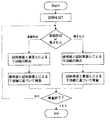
以上のような構成を備える試料検査装置において、以下にその動作を説明する。図3は検査動作のフローチャート図である。
【0026】
検査者は載置台13に試料6を配置して検査を開始する。試料6は載置台13に吸着保持されるのではなく、試料6の端部が数箇所で保持されるため、自然な反り状態を含む表面形状の平坦度を検査することができる。制御部11が光源1を発光させると、スクリーン7上には2つの干渉縞IS,ITが投影され、CCDカメラ9で撮像した画像はモニタ14に表示される。
【0027】
図2に示す2つの干渉縞像は、参照面5aと試料表面6aによる干渉縞ISと、試料表面6aと裏面6bによる干渉縞ITであり、検査者はモニタ14に表示される干渉縞IS,ITを基に試料形状を検査する。また、解析装置10はそれぞれの干渉縞IS,ITを基に表面形状及び厚さむらを定量的に演算解析し、測定する。以下、表面形状検査と厚さむら検査について、各々説明する。
【0028】
<表面形状検査>
表面形状検査では参照面5aと試料表面6aでの反射光による干渉縞ISを利用する。この際、試料表面6aと裏面6bでの反射光による干渉縞ITはノイズとなるため、精度の良い表面形状を得るためには、干渉縞ITの影響を取り除く、あるいは小さくすることが必要となる。
【0029】
この方法としては、光源1の光量を調節することで、干渉縞ITの影響を減少させることができる。具体的には図4の参照光の反射状況を説明する図に示すように、試料表面6aを通過した光が試料6内で吸収されるか、あるいは試料裏面6bで反射した光が試料表面6aを透過するまでの間に試料6内で吸収される程度の光量まで弱くする。光量の調節は検査者が手動により行うことができるが、干渉縞ITの明るさ(輝度)情報を検出し、予め設定した閾値以下になるように制御部11が光源1の光量を自動的に調節するようにすることも可能である。
【0030】
これにより、試料裏面6bからの反射光は試料表面6aでの反射光と干渉を起こすことなく試料6に吸収され、スクリーン7上に干渉縞ITは形成されなくなる。一方、干渉縞ITに対して干渉縞ISのコントラストは遥かに高いため、光源1の光量を落としても参照面5aと試料表面6aの反射光による干渉縞ISのみがCCDカメラ9に撮像される。
【0031】
また、試料6に投光される可干渉光の干渉性を低下させることでも裏面反射を除去することが可能である。例えば、測定光源1に半導体レーザ光源を用いる。半導体レーザ光源は通常1つのピーク波長を有しているが、温度が変化するとピーク波長が移行する特性がある。図5に示すように、通常1つのピーク波長λ1を有する参照光が(図5(a)参照)、温度変化によって波長λ1が弱まり、波長λ2が強くなり始める。一旦、2つの波長λ1,λ2の強度がほぼ等しくなった後(図5(b)参照)、ピーク波長λ2を有するようになるモードジャンプが生じる。(図5(c)参照)。
【0032】
裏面反射を除去する際には、図5(b)に示す2つの波長λ1,λ2がほぼ同じ強度を有する状態の参照光を利用する。ほぼ同じ強度を有する2つの波長λ1,λ2によるレーザ光の干渉性は弱まるため、干渉強度(コントラスト)が低い干渉縞ITは除され、参照面と試料表面での干渉縞ISが残るようになる。
【0033】
図6は、光源1を半導体レーザ光源とし、参照光の一部をビームスプリッタ30で分割し、センサ31で波長スペクトルを検出しながら、半導体レーザ光源への供給電力により温度を調節し、2つの波長強度がほぼ等しい参照光を投光することで、裏面反射による干渉縞ITを除去する例である。
【0034】
なお、試料6に投光される可干渉光の干渉性を低下させる手段としては、上記の他、図1におけるレンズ2とレンズ3の間にスリガラス板を配置した構成でも可能である。レンズ2の焦点をスリガラス板の拡散面からずらすことによって、点光源を見かけ上広げてレーザ光の干渉性を低下させるように調整できる。
【0035】
以上のように、干渉縞ITを除去又は減衰させることができれば、CCDカメラ9には表面形状情報が含まれた干渉縞ISだけが撮像されるので、干渉縞ISを基に公知の位相シフト法により試料表面形状を定量的に算出することができる。表面形状を得るための位相シフト法では、図示なきピエゾ素子を制御部11で駆動制御してプリズム5、又は載置台13を微妙に移動させ、参照面5aと試料表面6aとの距離を変化させる。この距離変化に応じて位相の異なる干渉縞像が形成されるので、位相の異なる複数の干渉縞像をCCDカメラ9で撮像し、メモリ15に記憶する。解析装置10では記憶された複数の干渉縞像を基に位相シフト法により試料表面形状を算出する。解析装置10により得られた試料表面形状データは鳥瞰図や各種情報としてモニタ14に表示される。
【0036】
<厚さむら検査>
厚さむら検査について説明する。厚さむら検査では試料表面6aと試料裏面6bでの反射光による干渉縞ITを利用する。厚さむら検査の場合には、参照面5aと試料表面6aでの反射光による干渉縞ISはノイズとなるため、厚さむらを精度良く検査する上で干渉縞ISを取り除く、あるいは減衰させてやる必要がある。
【0037】
検査者は干渉縞ISを除去するために、入力部12を操作して試料6が配置された載置台13を参照面5aに対して傾斜するように駆動する。その傾斜方向は、図7に示すように、試料表面6aに斜め方向から投光される測定光の光軸L1に対して試料表面上で直交する軸線L2方向である矢印A方向に傾斜させる。これにより、測定光の入射角度をほとんど変えることなく試料表面6aと参照面5aとの平行度を変更することができる。なお、載置台13の傾斜駆動は制御部11の制御により駆動装置17によって行われるが、回転ノブの操作等によって手動調整する構成でも良い。
【0038】
試料6を傾斜させると干渉縞ISの濃淡の間隔が密になり、干渉縞の数が多く形成される。さらに試料6の傾斜を大きくしていくと、干渉縞密度が順次密になり、干渉縞の間隔がCCDカメラ9の解像度(分解能)を越えると、CCDカメラ9では干渉縞ISが撮像されなくなる。このように干渉縞ISの間隔をCCDカメラ9の解像度以下にすることで干渉縞ISを実質的に除去することができる。また、試料6は測定光の光軸に対して試料表面上で直交する軸線方向に傾斜させているので、測定光の入射角は変更せず、傾斜による干渉縞ITへの影響(測定感度の影響)は殆どない。これにより、干渉縞ISのみが除去され、干渉縞ITのみがCCDカメラ9に撮像される。
【0039】
以上のように、干渉縞ISのみを除去することで、検査者はモニタ14に映出される干渉縞ITを基に精度良く検査を行うことができ、また、解析装置10では干渉縞ITを基に位相シフト法等を用いて演算解析することで、厚さむらを定量的に算出することができる。
【0040】
なお、干渉縞像ITに対して位相シフト法により演算解析する場合、干渉縞ISのように干渉を起こす2つの反射面の距離を変更することができないため、本実施形態ではロータリープリズム4を回転駆動して入射角を変更させることにより干渉縞を位相シフトさせ、複数の干渉縞を基に厚さむら情報を定量的に算出する。例えば、4ステップの位相シフト法では、試料へ投光される測定光の角度変化は、スクリーン7上に形成される干渉縞がπ/2分の位相だけ移動するように制御する。このようにして干渉縞の位相をπ/2分ずつ変化させた4枚の干渉縞画像を順次撮像し、これをメモリ15に記憶する。解析装置10はメモリ15に記憶した4枚の干渉縞画像から位相シフト法によって試料6の厚さむらの形状を解析する。
【0041】
また、解析装置10は定量的に算出した試料表面形状と厚さむら情報を基に、試料全体を三次元形状表示することが可能であり、検査者はモニタ14に表示される検査試料の情報を基に容易に検査を行うことができる。
【0042】
以上、1つの試料の表面形状と厚さむらの両方を検査する場合について説明したが、これに限らず本発明は次のように適用することができる。すなわち、半導体ウエハの表面形状を検査するために、測定光源1としてHe-Neレーザ等の可視光を使用した装置において、可視光を透過するガラスディスクの表面形状を検査したい場合、前述した方法により光源1の光量を弱くしたり、または測定光の干渉性を低下させる。これにより、可視光を透過するガラスディスクであっても、その表面と裏面での反射光による干渉縞の影響を取り除くことができ、ガラスディスクの表面形状の検査が可能となる。
【0043】
【発明の効果】
以上説明したように本発明によれば、装置構成を複雑とせずに、試料の自然な反り状態のままの表面形状、厚さむらを検査することができる。また、測定光を透過する試料であっても、ノイズとなる干渉縞を実質的に除去することで、表面形状を精度良く検査することができる。
【図面の簡単な説明】
【図1】実施形態である試料検査装置の要部概略図である。
【図2】スクリーン上に投影される干渉縞の説明図である。
【図3】検査動作のフローチャート図である。
【図4】参照光の反射状況を説明する図である。
【図5】半導体レーザ光源の温度変化による出射光の波長変化の説明図である。
【図6】裏面反射による干渉縞ITを除去する場合の変容例の要部概略図である。
【図7】干渉縞ISを除去する場合の試料(載置台)の傾斜方向を説明する図である。
【符号の説明】
1 光源
5 プリズム
5a 参照基準面
6 試料
6a 試料表面
6b 試料裏面
9 CCDカメラ
10 解析装置
11 制御部
13 載置台
15 メモリ
17 駆動装置[0001]
BACKGROUND OF THE INVENTION
The present invention relates to a sample inspection apparatus that inspects the shape of a sample based on interference fringes formed by coherent light projected onto the sample.
[0002]
[Prior art]
A sample inspection apparatus that projects measurement light of coherent light onto a sample such as a semiconductor wafer and inspects the surface shape of the sample based on an image obtained by imaging interference fringes generated by reflected light reflected from the sample surface and the reference surface It has been known. In such an apparatus, the back surface shape of the sample is made flat by bringing the back surface of the sample into close contact with a mounting table having a flat reference plane, and the surface shape (flatness) is measured.
[0003]
Also proposed is an apparatus that inspects thickness unevenness by projecting measurement light having the characteristics of transmitting through the sample, forming interference fringes by reflected light on the front and back surfaces of the sample, and inspecting the interference fringes. ing.
[0004]
[Problems to be solved by the invention]
However, in the case of the former apparatus, if the inspection is performed with the back surface of the sample adsorbed to the mounting table, the inspection itself is performed with the warpage and information of the sample corrected, so that natural warpage without thickness fluctuations occurs. The surface shape including the state could not be obtained.
[0005]
In order to inspect the surface shape including the natural warpage, the shape of the sample surface is inspected without adsorbing the back surface of the sample to the mounting table, and interference fringes caused by reflected light on the surface and back surface of the latter sample This is possible by combining inspections for obtaining thickness unevenness information based on the above, but if this is performed with separate inspection apparatuses, the inspection takes time and burdens on the inspector.
[0006]
When both inspections are performed with a single device, if light having the property of transmitting through the sample is used, both interference fringes formed on the reference surface and the sample surface and interference fringes formed on the front and back surfaces of the sample appear. Therefore, the other interference fringe influences as noise, making it difficult to perform a highly accurate inspection. As a method to avoid this, it is conceivable to use light that does not pass through the sample in the inspection of the surface shape, and use light that passes through the sample in the uneven thickness inspection, and separate the inspection optical paths of both. The method is complicated in configuration and the apparatus becomes large.
[0007]
In the former apparatus, it is difficult to inspect the surface shape of the sample that transmits the measurement light with high accuracy. For example, when using a device that inspects the surface shape of a semiconductor wafer with visible light such as a He-Ne laser and trying to inspect the surface shape of a glass disk, interference fringes are generated on the front and back surfaces of the glass disk. This makes accurate inspection difficult.
[0008]
An object of the present invention is to provide a sample inspection apparatus capable of accurately inspecting the surface shape and thickness unevenness of a sample without complicating the apparatus configuration in view of the above-described prior art.
[0009]
It is another object of the present invention to provide a sample inspection apparatus that can accurately inspect the surface shape of a sample that transmits measurement light.
[0010]
[Means for Solving the Problems]
In order to solve the above problems, the present invention is characterized by having the following configuration.
(1) In a sample inspection apparatus that projects coherent light from a measurement light source onto a sample and inspects the sample based on interference fringes formed by reflected light from the sample, the sample is arranged at a position facing the sample surface. Formed by the reference surface, the first interference fringes formed by the reflected light on the reference surface and the sample surface, and the reflected light reflected on the sample back surface after passing through the inside of the sample and the reflected light reflected on the sample surface screen and, first interference substantially removed imaging means for imaging the projected interference pattern on the screen, the first interference fringes projected on the screen together with the possible projection of the second interference fringes The fringe removing unit includes a tilting unit that tilts the sample relative to the reference surface, and the tilting unit makes the fringe density of the first interference fringes smaller than the resolution of the imaging unit. First interference fringe A first interference fringe removing unit that substantially removes the second interference fringe and a second interference fringe removing unit that substantially removes the second interference fringe projected on the screen, the coherent light projected on the sample A light amount adjusting means for adjusting the light amount of the light beam, the coherent light is attenuated by the light amount adjusting means, and the reflected light from the back surface of the sample is attenuated to substantially remove the second interference fringes, or A second interference that has adjustment means for adjusting the coherence of the coherent light projected on the sample, and that substantially eliminates the second interference fringes by reducing the coherence of the coherent light by the adjustment means; A fringe removing unit, an inspection unit for inspecting the shape of each sample based on the second interference fringe image remaining by the first interference fringe removing unit and the first interference fringe image remaining by the second interference fringe removing unit; It is characterized by providing.
(2) In the sample inspection apparatus of (1), the coherent light is projected from an oblique direction with respect to the sample, and the tilting unit causes the sample to be projected on the surface of the sample with respect to the projecting optical axis of the coherent light. It is characterized by inclining in the direction of an orthogonal axis.
[0021]
DETAILED DESCRIPTION OF THE INVENTION
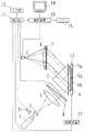
The present invention will be described below with reference to an embodiment. FIG. 1 is a schematic diagram of a main part of a sample inspection apparatus according to an embodiment. This device uses a grazing incidence interferometer.
[0022]
The coherent light emitted from the
[0023]
Part of the measurement light incident on the
[0024]
The interference fringe image formed on the
[0025]
The operation of the sample inspection apparatus having the above configuration will be described below. FIG. 3 is a flowchart of the inspection operation.
[0026]
The inspector places the
[0027]
The two interference fringe images shown in FIG. 2 are an interference fringe IS due to the
[0028]
<Surface shape inspection>
In the surface shape inspection, interference fringes IS caused by reflected light from the
[0029]
As this method, the influence of the interference fringe IT can be reduced by adjusting the light quantity of the
[0030]
Thereby, the reflected light from the sample back
[0031]
Further, it is also possible to remove the back surface reflection by reducing the coherence of the coherent light projected on the
[0032]
When removing back surface reflection, reference light in a state where the two wavelengths λ1 and λ2 shown in FIG. 5B have substantially the same intensity is used. Since the coherence of the laser light by the two wavelengths λ1 and λ2 having substantially the same intensity is weakened, the interference fringe IT having a low interference intensity (contrast) is excluded, and the interference fringe IS on the reference surface and the sample surface remains. .
[0033]
In FIG. 6, the
[0034]
In addition to the above, as a means for reducing the coherence of coherent light projected on the
[0035]
As described above, if the interference fringe IT can be removed or attenuated, only the interference fringe IS including the surface shape information is picked up by the
[0036]
<Thickness unevenness inspection>
The thickness unevenness inspection will be described. In the thickness unevenness inspection, interference fringes IT caused by reflected light from the
[0037]
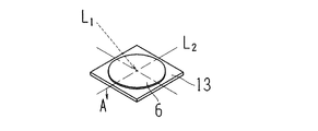
In order to remove the interference fringes IS, the inspector operates the
[0038]
When the
[0039]
As described above, by removing only the interference fringe IS, the inspector can accurately inspect based on the interference fringe IT displayed on the
[0040]
Note that when the interference fringe image IT is calculated and analyzed by the phase shift method, the distance between the two reflecting surfaces that cause interference cannot be changed as in the interference fringe IS. Therefore, in this embodiment, the
[0041]
Further, the
[0042]
The case where both the surface shape and the thickness unevenness of one sample are inspected has been described above, but the present invention is not limited to this and can be applied as follows. That is, in order to inspect the surface shape of the semiconductor wafer, in the apparatus using visible light such as a He—Ne laser as the
[0043]
【The invention's effect】
As described above, according to the present invention, it is possible to inspect the surface shape and thickness unevenness of a sample in a natural warpage state without complicating the apparatus configuration. Moreover, even if it is a sample which permeate | transmits measurement light, a surface shape can be test | inspected accurately by removing the interference fringe used as noise substantially.
[Brief description of the drawings]
FIG. 1 is a schematic view of a main part of a sample inspection apparatus according to an embodiment.
FIG. 2 is an explanatory diagram of interference fringes projected on a screen.
FIG. 3 is a flowchart of an inspection operation.
FIG. 4 is a diagram illustrating a reflection state of reference light.
FIG. 5 is an explanatory diagram of a wavelength change of emitted light due to a temperature change of a semiconductor laser light source.
FIG. 6 is a schematic diagram of a main part of a modification example in the case of removing interference fringes IT due to back surface reflection.
FIG. 7 is a diagram for explaining an inclination direction of a sample (mounting table) when interference fringes IS are removed.
[Explanation of symbols]
DESCRIPTION OF
Claims (2)
Priority Applications (1)
| Application Number | Priority Date | Filing Date | Title |
|---|---|---|---|
| JP30252999A JP4255586B2 (en) | 1999-10-25 | 1999-10-25 | Sample inspection equipment |
Applications Claiming Priority (1)
| Application Number | Priority Date | Filing Date | Title |
|---|---|---|---|
| JP30252999A JP4255586B2 (en) | 1999-10-25 | 1999-10-25 | Sample inspection equipment |
Publications (3)
| Publication Number | Publication Date |
|---|---|
| JP2001124532A JP2001124532A (en) | 2001-05-11 |
| JP2001124532A5 JP2001124532A5 (en) | 2006-11-30 |
| JP4255586B2 true JP4255586B2 (en) | 2009-04-15 |
Family
ID=17910072
Family Applications (1)
| Application Number | Title | Priority Date | Filing Date |
|---|---|---|---|
| JP30252999A Expired - Fee Related JP4255586B2 (en) | 1999-10-25 | 1999-10-25 | Sample inspection equipment |
Country Status (1)
| Country | Link |
|---|---|
| JP (1) | JP4255586B2 (en) |
Cited By (1)
| Publication number | Priority date | Publication date | Assignee | Title |
|---|---|---|---|---|
| JP7200220B2 (en) | 2017-04-28 | 2023-01-06 | 上海海立新能源技術有限公司 | scroll compressor for vehicle |
Families Citing this family (3)
| Publication number | Priority date | Publication date | Assignee | Title |
|---|---|---|---|---|
| JP2005049317A (en) | 2003-07-31 | 2005-02-24 | Nidek Co Ltd | Interferometer |
| JP4907201B2 (en) * | 2006-03-20 | 2012-03-28 | 株式会社神戸製鋼所 | Shape measuring device |
| CN111417834B (en) * | 2017-12-27 | 2022-07-12 | 中国涂料株式会社 | Measuring device and measuring method |
-
1999
- 1999-10-25 JP JP30252999A patent/JP4255586B2/en not_active Expired - Fee Related
Cited By (1)
| Publication number | Priority date | Publication date | Assignee | Title |
|---|---|---|---|---|
| JP7200220B2 (en) | 2017-04-28 | 2023-01-06 | 上海海立新能源技術有限公司 | scroll compressor for vehicle |
Also Published As
| Publication number | Publication date |
|---|---|
| JP2001124532A (en) | 2001-05-11 |
Similar Documents
| Publication | Publication Date | Title |
|---|---|---|
| US10254252B2 (en) | Surface and subsurface detection sensor | |
| KR102048793B1 (en) | Surface topography interferometer with surface color | |
| EP1840502B1 (en) | Optical interferometer for measuring changes in thickness | |
| TW479127B (en) | Method and device for measuring thickness of test object | |
| KR20130109365A (en) | Surface defect detecting apparatus and control method thereof | |
| JP4090860B2 (en) | 3D shape measuring device | |
| JPWO2009133849A1 (en) | Inspection device | |
| JP6531295B2 (en) | Reflected light detection device and reflected light detection method | |
| JP2005527820A (en) | Method and apparatus for determining the surface quality of a substrate sample using a differential interference contrast microscope | |
| JP4255586B2 (en) | Sample inspection equipment | |
| TW202204848A (en) | High sensitivity image-based reflectometry | |
| JP2001021810A (en) | Interference microscope | |
| JP2003042734A (en) | Method and apparatus for measurement of surface shape | |
| JPH10281876A (en) | Polarizing imaging system | |
| JP4605089B2 (en) | Surface inspection device | |
| JP4622933B2 (en) | Surface inspection method and surface inspection apparatus | |
| CN113763316A (en) | Image-based surface deformation metrology | |
| JP2005274156A (en) | Flaw inspection device | |
| JP5518187B2 (en) | Deformation measurement method | |
| EP0905508A2 (en) | Defect evaluation apparatus | |
| JP7480915B2 (en) | Defect inspection device and defect inspection method | |
| JP3848586B2 (en) | Surface inspection device | |
| JP3441408B2 (en) | Sample inspection device and sample inspection method | |
| JP4011205B2 (en) | Sample inspection equipment | |
| TWI818047B (en) | Testing equipment and testing methods |
Legal Events
| Date | Code | Title | Description |
|---|---|---|---|
| A521 | Written amendment |
Free format text: JAPANESE INTERMEDIATE CODE: A523 Effective date: 20061013 |
|
| A621 | Written request for application examination |
Free format text: JAPANESE INTERMEDIATE CODE: A621 Effective date: 20061013 |
|
| A977 | Report on retrieval |
Free format text: JAPANESE INTERMEDIATE CODE: A971007 Effective date: 20080828 |
|
| A131 | Notification of reasons for refusal |
Free format text: JAPANESE INTERMEDIATE CODE: A131 Effective date: 20080910 |
|
| A521 | Written amendment |
Free format text: JAPANESE INTERMEDIATE CODE: A523 Effective date: 20081110 |
|
| TRDD | Decision of grant or rejection written | ||
| A01 | Written decision to grant a patent or to grant a registration (utility model) |
Free format text: JAPANESE INTERMEDIATE CODE: A01 Effective date: 20090106 |
|
| A01 | Written decision to grant a patent or to grant a registration (utility model) |
Free format text: JAPANESE INTERMEDIATE CODE: A01 |
|
| A61 | First payment of annual fees (during grant procedure) |
Free format text: JAPANESE INTERMEDIATE CODE: A61 Effective date: 20090128 |
|
| FPAY | Renewal fee payment (event date is renewal date of database) |
Free format text: PAYMENT UNTIL: 20120206 Year of fee payment: 3 |
|
| R150 | Certificate of patent or registration of utility model |
Free format text: JAPANESE INTERMEDIATE CODE: R150 |
|
| FPAY | Renewal fee payment (event date is renewal date of database) |
Free format text: PAYMENT UNTIL: 20130206 Year of fee payment: 4 |
|
| FPAY | Renewal fee payment (event date is renewal date of database) |
Free format text: PAYMENT UNTIL: 20140206 Year of fee payment: 5 |
|
| R250 | Receipt of annual fees |
Free format text: JAPANESE INTERMEDIATE CODE: R250 |
|
| R250 | Receipt of annual fees |
Free format text: JAPANESE INTERMEDIATE CODE: R250 |
|
| LAPS | Cancellation because of no payment of annual fees |