JP4253365B2 - Wafer transfer device - Google Patents
Wafer transfer device Download PDFInfo
- Publication number
- JP4253365B2 JP4253365B2 JP28529097A JP28529097A JP4253365B2 JP 4253365 B2 JP4253365 B2 JP 4253365B2 JP 28529097 A JP28529097 A JP 28529097A JP 28529097 A JP28529097 A JP 28529097A JP 4253365 B2 JP4253365 B2 JP 4253365B2
- Authority
- JP
- Japan
- Prior art keywords
- wafer
- cassette
- transfer arm
- sensor
- transfer
- Prior art date
- Legal status (The legal status is an assumption and is not a legal conclusion. Google has not performed a legal analysis and makes no representation as to the accuracy of the status listed.)
- Expired - Lifetime
Links
Images


Classifications
-
- B—PERFORMING OPERATIONS; TRANSPORTING
- B65—CONVEYING; PACKING; STORING; HANDLING THIN OR FILAMENTARY MATERIAL
- B65G—TRANSPORT OR STORAGE DEVICES, e.g. CONVEYORS FOR LOADING OR TIPPING, SHOP CONVEYOR SYSTEMS OR PNEUMATIC TUBE CONVEYORS
- B65G49/00—Conveying systems characterised by their application for specified purposes not otherwise provided for
- B65G49/05—Conveying systems characterised by their application for specified purposes not otherwise provided for for fragile or damageable materials or articles
- B65G49/07—Conveying systems characterised by their application for specified purposes not otherwise provided for for fragile or damageable materials or articles for semiconductor wafers Not used, see H01L21/677
-
- H—ELECTRICITY
- H01—ELECTRIC ELEMENTS
- H01L—SEMICONDUCTOR DEVICES NOT COVERED BY CLASS H10
- H01L21/00—Processes or apparatus adapted for the manufacture or treatment of semiconductor or solid state devices or of parts thereof
- H01L21/67—Apparatus specially adapted for handling semiconductor or electric solid state devices during manufacture or treatment thereof; Apparatus specially adapted for handling wafers during manufacture or treatment of semiconductor or electric solid state devices or components ; Apparatus not specifically provided for elsewhere
- H01L21/67005—Apparatus not specifically provided for elsewhere
- H01L21/67242—Apparatus for monitoring, sorting or marking
- H01L21/67259—Position monitoring, e.g. misposition detection or presence detection
- H01L21/67265—Position monitoring, e.g. misposition detection or presence detection of substrates stored in a container, a magazine, a carrier, a boat or the like
-
- H—ELECTRICITY
- H01—ELECTRIC ELEMENTS
- H01L—SEMICONDUCTOR DEVICES NOT COVERED BY CLASS H10
- H01L21/00—Processes or apparatus adapted for the manufacture or treatment of semiconductor or solid state devices or of parts thereof
- H01L21/67—Apparatus specially adapted for handling semiconductor or electric solid state devices during manufacture or treatment thereof; Apparatus specially adapted for handling wafers during manufacture or treatment of semiconductor or electric solid state devices or components ; Apparatus not specifically provided for elsewhere
- H01L21/677—Apparatus specially adapted for handling semiconductor or electric solid state devices during manufacture or treatment thereof; Apparatus specially adapted for handling wafers during manufacture or treatment of semiconductor or electric solid state devices or components ; Apparatus not specifically provided for elsewhere for conveying, e.g. between different workstations
- H01L21/67763—Apparatus specially adapted for handling semiconductor or electric solid state devices during manufacture or treatment thereof; Apparatus specially adapted for handling wafers during manufacture or treatment of semiconductor or electric solid state devices or components ; Apparatus not specifically provided for elsewhere for conveying, e.g. between different workstations the wafers being stored in a carrier, involving loading and unloading
- H01L21/67778—Apparatus specially adapted for handling semiconductor or electric solid state devices during manufacture or treatment thereof; Apparatus specially adapted for handling wafers during manufacture or treatment of semiconductor or electric solid state devices or components ; Apparatus not specifically provided for elsewhere for conveying, e.g. between different workstations the wafers being stored in a carrier, involving loading and unloading involving loading and unloading of wafers
-
- Y—GENERAL TAGGING OF NEW TECHNOLOGICAL DEVELOPMENTS; GENERAL TAGGING OF CROSS-SECTIONAL TECHNOLOGIES SPANNING OVER SEVERAL SECTIONS OF THE IPC; TECHNICAL SUBJECTS COVERED BY FORMER USPC CROSS-REFERENCE ART COLLECTIONS [XRACs] AND DIGESTS
- Y10—TECHNICAL SUBJECTS COVERED BY FORMER USPC
- Y10S—TECHNICAL SUBJECTS COVERED BY FORMER USPC CROSS-REFERENCE ART COLLECTIONS [XRACs] AND DIGESTS
- Y10S414/00—Material or article handling
- Y10S414/135—Associated with semiconductor wafer handling
- Y10S414/137—Associated with semiconductor wafer handling including means for charging or discharging wafer cassette
Landscapes
- Engineering & Computer Science (AREA)
- Physics & Mathematics (AREA)
- Condensed Matter Physics & Semiconductors (AREA)
- General Physics & Mathematics (AREA)
- Manufacturing & Machinery (AREA)
- Computer Hardware Design (AREA)
- Microelectronics & Electronic Packaging (AREA)
- Power Engineering (AREA)
- Container, Conveyance, Adherence, Positioning, Of Wafer (AREA)
Description
【0001】
【発明の属する技術分野】
本発明は、ウェハカセットよりウェハを取出し搬送するウェハ搬送装置に関するものである。
【0002】
【従来の技術】
従来、ウェハカセットよりウェハを取出し搬送するウェハ搬送装置には、図7に示すように、エレベータ機構部1により上下動可能にしたカセット台2上に多数のウェハ3を積層方向に収容したウェハカセット4を載置していて、搬送開始の際に、エレベータ機構部1によりカセット台2を所定位置まで降下させ、図示しないセンサによりウェハカセット4内の搬送するウェハ3を検出し、搬送ウェハ3を検出したならば、エレベータ機構部1によりカセット台2を所定距離上昇させて搬送アーム5を搬送ウェハ3の下側に挿入し、次いで、エレベータ機構部1によりカセット台2を所定距離だけ降下させて、搬送アーム5によりウェハ3を吸着して、ウェハカセット4よりウェハ3を抜き取り、次の処理工程に供給するようにしたものがある。
【0003】
この場合、このようなウェハ搬送装置に用いられるウェハカセット4は、内部側壁に沿って複数のスロット溝6を形成していて、これらスロット溝6にウェハ3周縁を挿入することによりウェハ3を水平状態でウェハカセット4内に収容するようにしている。
【0004】
従って、ウェハカセット4内の全てのウェハ3が対応するスロット溝6に整然と水平状態に保持されていれば、搬送アーム5のウェハ3下側への挿入を正確に行うことができ、安定したウェハ3の抜き取り作業を実現することができる。
【0005】
ところが、実際は、スロット溝6への保持状態のバラツキなどによりウェハ3が傾いて挿入されることがあり、このウェハ3の傾きにより、搬送アーム5のウェハ3下側への挿入の際に、搬送アーム5がウェハ3に衝突し、ウェハ3を破損してしまうという問題があった。
【0006】
そこで、従来、特許第2606423号公報に開示されるようにウェハのスロット溝に挿入される両端部を検出するように、2個のセンサを同じ高さで並べて設け、それぞれのセンサによるウェハ検出が同時ならば、ウェハが水平に保持されているものとして、そのままウェハ下側に搬送アームを挿入し、また、それぞれのセンサによるウェハ検出に時間的ずれがあれば、ウェハが傾いて保持されているものとして、この傾きを考慮してウェハ下側に搬送アームを挿入することにより、搬送アーム5がウェハ3に衝突するのを防止するようにしたものが考えられている。
【0007】
【発明が解決しようとする課題】
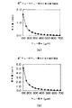
ところで、最近、ウェハの大形化と薄形化にともない、ウェハカセット内に収容されるウェハの撓みが問題になっており、6インチウェハや8インチウェハを例にとっても、それぞれ図8(a)(b)に示すようにウェハ厚みの薄形化にともない、撓み量が急激に増加することが知られている。
【0008】
ところが、従来のようにウェハのスロット溝に挿入される両端部を検出するようにセンサを配置したものでは、ウェハの傾きは検出できるが、最も撓んでいる位置、つまりウェハの中央部を検出できないため、搬送アームをウェハ下側に挿入したときに、搬送アーム5とウェハ3の最も撓んでいる位置が干渉し、ウェハ破損を生じるおそれがある。
【0009】
また、ウェハの中央部の最も撓んでいる位置を検出できないことから、搬送しようとするウェハと1段下のウェハの丁度中間に搬送アームを挿入したとすると、1段下のウェハ上面に搬送アームが接触し、ウェハ面を傷付けてしまうおそれがある。
【0010】
さらに、ウェハが吸着できたことを確認した場所でエレベータの移動を停止し、ウェハを取り出す状態で、ウェハが薄く大きく撓んでいると、ウェハの最も撓んでいる位置に搬送アームが接触したとしても、ウェハ周縁部がスロット溝から離れることができず、ウェハ下面がスロット溝に擦られた状態で引き出されるため、ウェハが破損したり、発塵の原因になることもある。
【0011】
さらに、ウェハを取り出した位置を記憶しておき、再度この位置にウェハを格納しようとすると、ウェハ周縁部がスロット溝と干渉し、ウェハ破損を生じるおそれがある。
【0012】
さらに、搬送アームは、ウェハカセット内に挿入されるため、ウェハの径より小さい寸法にならざるをえなく、搬送アームにウェハを乗せた時に、ウェハ周縁部が搬送アーム上部より下側に撓んでしまう。この撓み量は、搬送アームがウェハを支持する範囲によっても異なるため、この搬送アーム上でのウェハ吸着状態におけるウェハ周縁部での撓み量を考慮しないと、ウェハ取り出し時には、ウェハ下面がスロット溝に擦れた状態のまま引き出され、ウェハが破損したり、発塵が生ずるおそれがあり、ウェハ収納時には、ウェハ周縁部がスロット溝と干渉し、ウェハを破損してしまうおそれがある。
【0013】
さらに、ウェハカセット内の最下段のウェハを取り出す場合、ウェハが撓んでいることにより、カセット下部の連結部材の厚みによっては、ウェハ下面と連結部材との間隔が極端に狭くなり、この状態で、搬送アームを挿入すると、連結部材と搬送アームが干渉し、搬送アームを破損してしまうおそれがある。
本発明は、上記事情に鑑みてなされたもので、ウェハ搬送時のウェハの破損を確実に防止できるウェハ搬送装置を提供することを目的とする。
【0014】
【課題を解決するための手段】
請求項1記載の発明は、複数のウェハを収納可能なウェハカセットと、このウェハカセットに対して相対的に上下動可能であって所望のウェハを下側から支持してウェハカセットに対する出し入れを行う搬送アームとを備えるウェハ搬送装置において、
前記ウェハカセットに対して相対的に上下動可能であって、かつ搬送するウェハおよび該ウェハの上下方向のウェハのウェハ中央部の位置を検出するセンサと、このセンサを挟んで前記ウェハのウェハカセットに支持される周縁部の位置を検出する2個のセンサとを有する位置検出手段を有し、この位置検出手段で検出された各ウェハの位置情報に基づいて各ウェハの撓み量を求めるとともに、前記搬送するウェハ下側への前記搬送アームの挿入の可能性および前記搬送アームによるウェハの所定ストロークの持ち上げの可能性を判断するようにしている。
【0017】
この結果、本発明によれば、位置検出手段で検出された各ウェハの位置情報に基づいて各ウェハの撓み量を求められるので、ウェハカセット内の各ウェハの撓み量が異なっていても、搬送時に搬送アームがウェハに接触したり、ウェハ同士が接触したりして、ウェハ面に傷を付けたり、破損させてしまうような危険性を回避することができる。
【0020】
【発明の実施の形態】
以下、本発明の実施の形態を図面に従い説明する。
(第1の実施の形態)
図1は、本発明が適用されるウェハ搬送装置の概略構成を示している。図において、11はエレベータ機構部で、このエレベータ機構部11には、カセット台12を載置し、エレベータ機構部11によりカセット台12を上下方向に移動可能にしている。
【0021】
このようなカセット台12上にウェハカセット13を載置している。このウェハカセット13は、内部側壁に沿って多数のスロット溝14を形成し、これらスロット溝14にウェハ15周縁部を挿入することにより、ウェハ15を水平状態でウェハカセット13内の積層方向に収容するようにしている。
【0022】
カセット台12上に載置されたウェハカセット13に対する所定の高さ位置に、ウェハカセット13に収容されたウェハ15を検出するセンサA16、センサB17を設けている。このうち、センサA16は、発光部161と受光部162をウェハカセット13の前後方向に配置した光透過型センサからなるもので、ウェハカセット13内のウェハ15の撓みの大きい中央部を検出可能に配置している。また、センサB17も、発光部171と受光部172をウェハカセット13の前後方向に配置した光透過型センサからなるもので、センサA16に対して水平方向に同じ高さに設けられ、センサA16で検出されると同じウェハ15のスロット溝14へ挿入される周縁部を検出可能にしている。
【0023】
そして、ウェハカセット13に対応して搬送アーム18を設けている。この搬送アーム18は、ウェハ15を吸着する複数の吸着口181を有し、搬送するウェハ15の下側に挿入されるとともに、吸着口181によりウェハ15を吸着して、ウェハカセット13より抜き取り、所定の処理の終了後、再びウェハカセット13内の元の位置に戻すようにしている。
【0024】
次に、このように構成した実施の形態の動作を説明する。
この場合、エレベータ機構部11により上下動可能にしたカセット台12上にウェハカセット13を載置し、図示しないスイッチを投入してウェハ搬送開始を指示すると、図2に示すフローが実行される。
【0025】
まず、ステップ201で、エレベータ機構部11によりカセット台12を搬送開始位置まで下降する。次いで、ステップ202で、センサA16によりウェハカセット13内のn−1番目のウェハ15を検出する。この状態を図3(a)に示している。ここで、n−1番目のウェハ15が検出されない場合は、ステップ203で、ウェハカセット13を、さらに降下させてn−1番目のウェハ15が検出されるまで同じ動作を繰り返す。
【0026】
そして、ステップ202で、n−1番目のウェハ15を検出すると、ステップ204で、今度は、センサB17によりセンサA16で検出したと同様のn−1番目のウェハ15を検出する。この状態を図3(b)に示している。ここでも、n−1番目のウェハ15が検出されない場合は、ステップ205で、ウェハカセット13を、さらに降下させてn−1番目のウェハ15が検出されるまで同じ動作を繰り返す。
【0027】
次いで、ステップ206で、n−1番目のウェハ15の撓み状態を判断し、図示しない記憶部に記憶する。ここで、センサA16が検出したn−1番目のウェハ15の位置情報をn−1a、センサB17が検出したn−1番目のウェハ15の位置情報をn−1bとすると、これらセンサA16、センサB17による位置情報n−1aとn−1bが同じの場合は、ウェハカセット13内のウェハ15は、水平状態(ウェハ15の自重による撓みが発生していない)と判断し、図示しない記憶部に記憶し、また、センサA16、センサB17による位置情報n−1aとn−1bが異なる場合は、これらの差を撓み状態として図示しない記憶部に記憶する。
【0028】
次に、ステップ207で、センサA16によりウェハカセット13内のn番目のウェハ15を検出する。この状態を図3(c)に示している。ここで、n番目のウェハ15が検出されない場合は、ステップ208で、ウェハカセット13を、さらに降下させてn番目のウェハ15が検出されるまで同じ動作を繰り返す。
【0029】
そして、ステップ207で、n番目のウェハ15を検出すると、ステップ209で、今度は、センサB17によりセンサA16で検出したと同様のn番目のウェハ15を検出する。この状態を図3(d)に示している。ここでも、n番目のウェハ15が検出されない場合は、ステップ210で、ウェハカセット13を、さらに降下させてn番目のウェハ15が検出されるまで同じ動作を繰り返す。
【0030】
次に、ステップ211で、n番目のウェハ15の撓み状態を判断し、図示しない記憶部に記憶する。ここで、センサA16が検出したn番目のウェハ15の位置情報をna、センサB17が検出したn番目のウェハ15の位置情報をnbとすると、これらセンサA16、センサB17による位置情報naとnbが同じの場合は、ウェハカセット13内のウェハ15は、水平状態(ウェハ15の自重による撓みが発生していない)と判断し、図示しない記憶部に記憶し、また、センサA16、センサB17による位置情報naとnbが異なる場合は、これらの差を撓み状態として図示しない記憶部に記憶する。
【0031】
次に、ステップ212で、n番目のウェハ15を搬送アーム18で吸着した場合、n番目のウェハ15の外周部がどの程度撓むかの計算を行うとともに、撓んだn番目のウェハ15外周部がウェハカセット13のストローク溝14の所定高さまで持ち上げられるに必要なウェハ吸着ストロークPを決定し、さらに、ステップ213で、n番目のウェハ15が撓んでいる場合、搬送アーム18の挿入可能の間隔が狭くなるため、n−1番目のウェハ15上面とn番目のウェハ15の下面との間に搬送アーム18が挿入できるかを位置情報n−1a、n−1b、naとnbを用いて計算する。つまり、図4(a)に示すように搬送アーム18上面とn番目のウェハ15下面との間のクリアランスaと搬送アーム18下面と、n−1番目のウェハ15上面との間のクリアランスbの存在を計算によりを確認する。
【0032】
そして、ステップ214で、この時の計算結果から搬送アーム18の挿入が可能か否か判断し、挿入が不可能であれば、n番目のウェハ15の搬送は行わないものとして、ステップ202に戻って上述したと同様な動作を行う。
【0033】
これにより、ウェハカセット13内で撓んでいるn−1番目のウェハ15の上面とn番目のウェハ15の下面との間に搬送アーム18が挿入できない場合は、搬送アーム18の無理な挿入を防止できるので、搬送アーム18によりn−1番目のウェハ15上面に傷を付けたり、破損させてしまうような危険性を回避することができる。
【0034】
一方、搬送アーム18の挿入が可能であれば、ステップ215で、n−1番目のウェハ15とn番目のウェハ15の中間を、n番目のウェハ15の取り出し時の搬送アーム18の挿入高さEとして、図示しない記憶部に記憶する。
【0035】
次に、ステップ216で、エレベータ機構部11によりカセット台12を降下させ、ステップ217で、センサA16によりウェハカセット13内のn+1番目のウェハ15を検出する。この状態を図3(e)に示している。ここで、n+1番目のウェハ15が検出されない場合は、ステップ218で、ウェハカセット13を、さらに降下させてn+1番目のウェハ15が検出されるまで同じ動作を繰り返す。
【0036】
そして、ステップ217で、n+1番目のウェハ15を検出すると、ステップ219で、今度は、センサB17によりセンサA16で検出したと同様のn+1番目のウェハ15を検出する。この状態を図3(f)に示している。ここでも、n+1番目のウェハ15が検出されない場合は、ステップ220で、ウェハカセット13を、さらに降下させてn+1番目のウェハ15が検出されるまで同じ動作を繰り返す。
【0037】
次いで、ステップ221で、n+1番目のウェハ15の撓み状態を判断し、図示しない記憶部に記憶する。ここで、センサA16が検出したn+1番目のウェハ15の位置情報をn+1a、センサB17が検出したn+1番目のウェハ15の位置情報をn−1bとすると、これらセンサA16、センサB17による位置情報n+1aとn+1bが同じの場合は、ウェハカセット13内のウェハ15は、水平状態と判断し、図示しない記憶部に記憶し、また、センサA16、センサB17による位置情報n+1aとn+1bが異なる場合は、これらの差を撓み状態として図示しない記憶部に記憶する。
【0038】
次に、ステップ222で、n番目のウェハ15を搬送アーム18によりウェハ吸着ストロークPだけ持ち上げた場合、n+1番目のウェハ15下面とn番目のウェハ15上面との間にクリアンスがあるか計算を行う。つまり、図4(b)に示すようにn番目のウェハ15を搬送アーム18により持ち上げた時、n+1番目のウェハ15下面とn番目のウェハ15上面との間にクリアンスcが存在するかを計算によりを確認する。
【0039】
そして、ステップ223で、この時の計算結果から、吸着ストロークPに必要なクリアランスが有るか否か判断し、挿入が不可能であれば、n番目のウェハ15の搬送は行わないものとして、ステップ202に戻って上述したと同様な動作を行う。
【0040】
これにより、ウェハカセット13内で撓んでいるn番目のウェハ15を吸着ストロークPだけ持ち上げたときに、n番目のウェハ15上面がn+1番目のウェハ15下面に接触することを防止できるので、これらn番目およびn+1番目のウェハ15に傷を付けたり、破損させてしまうような危険性を回避することができる。
【0041】
一方、十分なクリアランスを確保できる場合は、ステップ224で、エレベータ機構部11によりカセット台12をn番目のウェハ15の取り出し時の搬送アーム18の挿入高さHまで降下させる。
【0042】
次いで、ステップ225で、搬送アーム18をn番目のウェハ15の下側に挿入し、ステップ226で、エレベータ機構部11によりカセット台12を吸着ストロークPだけ下げ、搬送アーム18によりn番目のウェハ15を吸着し、ステップ227で、搬送アーム18によりウェハカセット13よりn番目のウェハ15を取り出し、ステップ228で、装置の用途に応じた処理を実行する。
【0043】
処理の終了後、ステップ229で、n番目のウェハ15の取り出し時と同じ位置に搬送アーム18を挿入するとともに、搬送アーム18による吸着を解除する。
【0044】
そして、ステップ230で、搬送アーム18がn番目のウェハ15を吸着するために下げた吸着ストロークPだけカセット台12を上げて、ウェハ15をウェハカセット13のスロット溝14中に受け渡し、ステップ231で、搬送アーム18を待機位置に移動して、n番目のウェハ15の搬送処理を終了し、以下、ステップ232で、ウェハカセット13に納められている全てのウェハ15について処理終了を判断するまで、上述したと同様な処理を繰り返すようになる。
【0045】
従って、このようにすれば、エレベータ機構部11により上下動可能にしたウェハカセット13内に多数のウェハ15を積層方向に収容し、ウェハカセット13内の搬送するウェハ15下側より搬送アーム18を挿入し保持することで、ウェハカセット13より出し入れ可能にしたもので、ウェハカセット13に対する所定の高さ位置にセンサA16、センサB17を設け、これらセンサA16、センサB17により、エレベータ機構部11によりウェハカセット13を上下動して、搬送するn番目のウェハ15と、このn番目のウェハ15に対し上下方向に位置されるn−1、n+1番目のウェハ15の、それぞれの撓みの大きい中央部とウェハカセット13のスロット溝14への支持部の位置を検出し、この検出されたn−1、n、n+1番目のウェハ15の位置情報により、これらウェハ15の撓み量を求めるとともに、搬送アーム18の搬送するn番目のウェハ下側への挿入の可能性およびn番目のウェハをウェハ吸着ストロークでの持ち上げの可能性を判断するようにしたので、仮に、ウェハカセット13内の各ウェハ15の撓み量が異なっていても、搬送アーム18が誤ってウェハに接触したり、ウェハ15同士が接触したりして、ウェハ15面に傷を付けたり、破損させてしまうような危険性を確実に回避することができる。また、各ウェハ15について、撓みの大きい中央部とウェハカセット13のスロット溝14への支持部の2箇所で位置検出をしているので、撓み量が異なるウェハ15についても,それそぞれ正確に撓み量を求めることができる。
【0046】
なお、上述した実施の形態では、n番目のウェハ15をウェハカセット13から取り出す場合を述べたが、装置のスループットを向上させるために、最初にエレベータ機構部11によりカセット台12を降下させるとともに、ウェハカセット13内ウェハ15の全ての撓み状態を検出し、その情報を図示しない記憶部に記憶し、搬送可能と判断したウェハ15のみをウェハカセット13から取り出し、次の処理を実行し、搬送不可能と判断したウェハ15については、搬送を行わないで、エレベータ機構部11をスキップさせることも可能である。
【0047】
また、ウェハカセット13の最下段のウェハ15を処理する場合において、最下段ウェハ15の下方に位置されるウェハカセット13下部の連結部材の上面の状態を検出することで、連結部材上面と最下段のウェハ15の下面の間隔がわかり、搬送アーム18が挿入可能かの情報を得ることができる。
【0048】
さらに、上述した実施の形態では、ウェハカセット13内のウェハ15の撓みの大きい中央部を検出可能にしたセンサA16と、同じウェハ15のスロット溝14へ挿入される周縁部を検出可能にしたセンサB17を設ける場合を述べたが、ウェハカセット13内のウェハ15の撓みの大きい中央部を検出可能にしたセンサA16のみを設けたものにも適用できる。この場合は、センサB17によるウェハ15のスロット溝14へ挿入される周縁部の検出位置情報に代えて、ウェハカセット13の高さ位置を基準として用いるようにすればよい。
(第2の実施の形態)
第1の実施の形態では、センサA16がウェハカセット13内のウェハ15の中心位置に配置することにより、ウェハ15中央の一番撓みの大きな場所を検出するようにしたが、必ずしもセンサA16は、ウェハ15の中心位置に配置しなくとも、センサA16、センサB17の位置関係と検出時の高低差から、内部演算によってウェハ15の撓み量を予測しても、上述した第1の実施の形態と同様な効果が得られる。
(第3の実施の形態)
上述した第1の実施の形態では、2個のセンサA16、センサB17によりウェハ15の撓み値を検出しているが、仮に、ウェハカセット13内で、ウェハ15が同じ高さのスロット溝14に挿入されず、斜めの状態で保持されることがあると、ウェハ15の取り出し時に、搬送アーム18とウェハ15が干渉してウェハ15を破損する危険性がある。
【0049】
そこで、この第3の実施の形態では、図5(a)(b)に示すようにセンサ16、17に加えて、さらにウェハ15のセンサ16を挟んで反対側のスロット溝14へ挿入される周縁部を検出するセンサC19を設けている。つまり、ウェハカセット13の中心位置には、センサA16が配置され、このセンサA16を挟んだ左右対称位置にセンサB17、センサC19を配置するようにしている。
【0050】
このような構成によれば、エレベータ機構部11によりカセット台12を降下させた時、図5(a)に示すようにウェハカセット13内ウェハ15をセンサA16、センサB17が検出するものの、センサC19がウェハ15を検出しない場合、または、同図(b)に示すようにセンサC19がウェハカセット13内ウェハ15を検出するものの、センサA16、センサB17がウェハ15を検出しない場合は、図示しない制御部によりウェハカセット13内ウェハ15が正規の状態で、ウェハカセット13内に治められていなかったと判断して、搬送アーム18をウェハカセット13内部に挿入しないようにしている。これにより、ウェハカセット13内に正規の状態で保持されていないウェハ15を搬送アームで破損するような危険性を回避できる。
(第4の実施の形態)
上述した第1の実施の形態では、ウェハカセット13の前後方向にセンサA16、センサB17を配置したが、装置の構成上、センサの配置できるスペースが無い場合もある。
【0051】
そこで、この第4の実施の形態では、図6に示すように、ウェハ15を収容するウェハカセット13のカセット台12下部に3個の距離測定センサ20、21、22をウェハカセット13前面に対して平行な方向に並べて配置する。
【0052】
このような構成によれば、ウェハ15を収容したウェハカセット13がカセット台12上に載置されると、距離測定センサ20、21、22の3箇所で、ウェハカセット13下面からウェハ15下面までの距離を測定し、これら距離測定センサ20、21、22の測定結果から、図示しない制御部によりウェハカセット13内のウェハ15の撓み状態を判断し、予め記憶している搬送アームの挿入高さ、吸着ストロークが決定される。これにより、仮に、ウェハカセット13内に薄いウェハ15が挿入されても、第1の実施の形態と同様に、ウェハ15を搬送アームで破損してしまうような危険性を回避できる。また、ウェハカセット13をカセット台12に載置することで、カセット台12を上下動させることなく、ウェハカセット13のウェハ15の厚みを非接触で検出できるので、タクトタイムを短くすることも可能になる。
【0053】
上述した各実施の形態では、エレベータ機構部11によりウェハカセット13を上下動させてウェハ15の出し入れを行っているが、カセット台12およびウェハカセット13を固定して搬送アーム18を上下させることによりウェハ15の出し入れを行うようにした装置に対しても、本発明は同様に適用できる。この場合、各実施の形態におけるウェハ検出用センサ(センサA、センサB、センサC)も上下させるようにする。これらセンサの上下動の方法としては、搬送アーム18とは独立して上下動させる方法と、搬送アーム18と一体的に上下動させる方法のいずれでもよい。センサと搬送アーム18を一体的に上下動させる方法は、上下動機構が一つで済むので、装置の簡素化に有効である。
【0054】
なお、上述した実施の形態には、以下の発明も含まれている。
(1)エレベータ機構部により上下動可能にしたウェハカセット内に多数のウェハを積層方向に収容し、該ウェハカセット内の搬送するウェハ下側より搬送アームを挿入し保持することで、ウェハカセットより出し入れ可能にしたウェハ搬送装置において、
前記ウェハカセットに対する所定の高さ位置に設けられ、搬送するウェハ、該ウェハの上下方向のウェハの、それぞれの少なくとも中央部の位置を検出する位置検出手段を有し、この位置検出手段で検出された各ウェハの位置情報に基づいて各ウェハの撓み量を求めるとともに、搬送するウェハ下側への前記搬送アームの挿入の可能性および前記搬送アームによるウェハの所定ストロークの持ち上げの可能性を判断することを特徴とするウェハ搬送装置。
【0055】
【発明の効果】
以上述べたように本発明によれば、位置検出手段で検出された各ウェハの位置情報により求められた各ウェハの撓み量が求められるので、ウェハカセット内の各ウェハの撓み量が異なっていても、搬送時に挿入される搬送アームがウェハに接触したり、ウェハ同士が接触したりして、ウェハ面に傷を付けたり、破損させてしまうような危険性を回避することができる。
【0056】
また、各ウェハについて、撓みの大きい中央部とウェハカセットへの支持部の2箇所で位置検出ができるので、撓み量が異なる各ウェハについても正確に撓み量を求めることができる。
【0057】
さらに、ウェハがウェハカセットの同じ高さのスロット溝に挿入されず、斜めの状態で保持されることがあっても、この状態を検出して、搬送アームをウェハカセット内部に挿入しないようにでき、搬送アームの挿入によるウェハの破損を防止できる。
【図面の簡単な説明】
【図1】 本発明の第1の実施の形態の概略構成を示す図。
【図2】 第1の実施の形態の動作を説明するフローチャート。
【図3】 第1の実施の形態の動作を説明するための図。
【図4】 第1の実施の形態の動作を説明するための図。
【図5】 本発明の第3の実施の形態を説明するための図。
【図6】 本発明の第4の実施の形態を説明するための図。
【図7】 従来のウェハ搬送装置を説明するための図。
【図8】 ウェハの厚みと撓み量の関係を説明するための図。
【符号の説明】
11…エレベータ機構部、
12…カセット台、
13…ウェハカセット、
14…スロット溝、
15…ウェハ、
16…センサA、
17…センサB、
18…搬送アーム、
19…センサC、
20、21、22…距離測定センサ。[0001]
BACKGROUND OF THE INVENTION
The present invention relates to a wafer transfer apparatus that takes out and transfers a wafer from a wafer cassette.
[0002]
[Prior art]
2. Description of the Related Art Conventionally, as shown in FIG. 7, in a wafer transfer apparatus for taking out and transferring wafers from a wafer cassette, a wafer cassette in which a large number of
[0003]
In this case, the
[0004]
Accordingly, if all the
[0005]
However, in reality, the
[0006]
Therefore, conventionally, as disclosed in Japanese Patent No. 2606423, two sensors are arranged side by side at the same height so as to detect both ends inserted into the slot groove of the wafer, and wafer detection by each sensor is performed. At the same time, assuming that the wafer is held horizontally, the transfer arm is inserted as it is under the wafer, and if there is a time lag in wafer detection by each sensor, the wafer is held tilted. In consideration of this inclination, it is considered that the transfer arm 5 is prevented from colliding with the
[0007]
[Problems to be solved by the invention]
Recently, with the increase in size and thickness of wafers, the bending of wafers accommodated in wafer cassettes has become a problem. For example, 6-inch wafers and 8-inch wafers are shown in FIG. As shown in (b), it is known that the amount of bending increases rapidly as the wafer thickness is reduced.
[0008]
However, in the case where the sensor is arranged so as to detect both ends inserted into the slot groove of the wafer as in the prior art, the tilt of the wafer can be detected, but the most bent position, that is, the central portion of the wafer cannot be detected. Therefore, when the transfer arm is inserted on the lower side of the wafer, the position where the transfer arm 5 and the
[0009]
In addition, since the most bent position of the central portion of the wafer cannot be detected, if the transfer arm is inserted just between the wafer to be transferred and the next lower wafer, the transfer arm is placed on the upper surface of the lower wafer. May come in contact and damage the wafer surface.
[0010]
Furthermore, if the wafer is thin and greatly bent in a state where the movement of the elevator is stopped and the wafer is taken out at a place where it is confirmed that the wafer has been attracted, even if the transfer arm comes into contact with the most bent position of the wafer The peripheral edge of the wafer cannot be separated from the slot groove, and the lower surface of the wafer is pulled out while being rubbed against the slot groove. Therefore, the wafer may be damaged or dust may be generated.
[0011]
Further, if the position where the wafer has been taken out is stored and an attempt is made to store the wafer again at this position, the peripheral edge of the wafer may interfere with the slot groove, possibly causing damage to the wafer.
[0012]
Furthermore, since the transfer arm is inserted into the wafer cassette, the size of the transfer arm must be smaller than the diameter of the wafer. When the wafer is placed on the transfer arm, the peripheral edge of the wafer is bent downward from the upper part of the transfer arm. End up. Since the amount of deflection differs depending on the range in which the transfer arm supports the wafer, the lower surface of the wafer becomes a slot groove when the wafer is taken out without considering the amount of deflection at the wafer peripheral edge in the wafer adsorption state on the transfer arm. The wafer may be pulled out while being rubbed, and the wafer may be damaged or dust may be generated. When the wafer is stored, the peripheral edge of the wafer may interfere with the slot groove and the wafer may be damaged.
[0013]
Furthermore, when taking out the lowermost wafer in the wafer cassette, due to the bending of the wafer, depending on the thickness of the connecting member at the bottom of the cassette, the distance between the lower surface of the wafer and the connecting member becomes extremely narrow. When the transfer arm is inserted, the connecting member and the transfer arm may interfere with each other and the transfer arm may be damaged.
The present invention has been made in view of the above circumstances, and an object of the present invention is to provide a wafer transfer apparatus that can reliably prevent damage to the wafer during wafer transfer.
[0014]
[Means for Solving the Problems]
According to the first aspect of the present invention, a wafer cassette that can store a plurality of wafers, and can be moved up and down relative to the wafer cassette, and a desired wafer is supported from the lower side to be taken in and out of the wafer cassette. In a wafer transfer device comprising a transfer arm,
The wafer can be moved up and down relative to the wafer cassette, and the wafer to be transferred and the wafer in the vertical direction of the wafer A sensor for detecting the position of the central portion of the wafer, and two sensors for detecting the position of the peripheral portion of the wafer supported by the wafer cassette across the sensor. A position detection unit is provided, and a deflection amount of each wafer is obtained based on the position information of each wafer detected by the position detection unit. At the same time, the possibility of inserting the transfer arm below the wafer to be transferred and the possibility of lifting a predetermined stroke of the wafer by the transfer arm are determined. I am doing so.
[0017]
As a result, Book According to the invention, the amount of deflection of each wafer can be obtained based on the position information of each wafer detected by the position detection means. Ru Therefore, even if the deflection amount of each wafer in the wafer cassette is different, the transfer arm may come into contact with the wafer during the transfer, or the wafers may come into contact with each other, causing the wafer surface to be damaged or damaged. Danger can be avoided.
[0020]
DETAILED DESCRIPTION OF THE INVENTION
Hereinafter, embodiments of the present invention will be described with reference to the drawings.
(First embodiment)
FIG. 1 shows a schematic configuration of a wafer transfer apparatus to which the present invention is applied. In the figure, reference numeral 11 denotes an elevator mechanism, and a
[0021]
A
[0022]
Sensors A16 and B17 for detecting the
[0023]
A
[0024]
Next, the operation of the embodiment configured as described above will be described.
In this case, when the
[0025]
First, in step 201, the elevator mechanism unit 11 lowers the cassette table 12 to the conveyance start position. Next, at
[0026]
Then, when the n-
[0027]
Next, in step 206, the bending state of the (n-1)
[0028]
In
[0029]
When the n-
[0030]
Next, in step 211, the bending state of the
[0031]
Next, in
[0032]
In step 214, it is determined whether or not the
[0033]
Thereby, when the
[0034]
On the other hand, if the
[0035]
Next, in
[0036]
When the n +
[0037]
Next, in step 221, the bending state of the (n + 1)
[0038]
Next, in step 222, when the
[0039]
In step 223, it is determined from the calculation result at this time whether or not the clearance required for the suction stroke P is present. If the insertion is impossible, the n-
[0040]
Thus, when the
[0041]
On the other hand, if a sufficient clearance can be ensured, in step 224, the elevator mechanism 11 lowers the cassette table 12 to the insertion height H of the
[0042]
Next, in step 225, the
[0043]
After the processing is completed, in step 229, the
[0044]
In step 230, the
[0045]
Therefore, in this way, a large number of
[0046]
In the above-described embodiment, the case where the n-
[0047]
Further, when processing the
[0048]
Further, in the above-described embodiment, the sensor A16 that can detect the central portion of the
(Second Embodiment)
In the first embodiment, the sensor A16 is arranged at the center position of the
(Third embodiment)
In the first embodiment described above, the deflection value of the
[0049]
Therefore, in the third embodiment, in addition to the
[0050]
According to such a configuration, when the cassette table 12 is lowered by the elevator mechanism 11, the sensor A16 and the sensor B17 detect the
(Fourth embodiment)
In the first embodiment described above, the sensors A16 and B17 are arranged in the front-rear direction of the
[0051]
Therefore, in the fourth embodiment, as shown in FIG. 6, three
[0052]
According to such a configuration, when the
[0053]
In each of the embodiments described above, the
[0054]
The embodiments described above also include the following inventions.
(1) A large number of wafers are accommodated in the stacking direction in a wafer cassette that can be moved up and down by an elevator mechanism, and a transfer arm is inserted and held from below the wafer to be transferred in the wafer cassette. In the wafer transfer device that can be put in and out,
Position detection means provided at a predetermined height position with respect to the wafer cassette and detecting the position of at least the central portion of each of the wafer to be transferred and the wafer in the vertical direction of the wafer, and is detected by this position detection means. Further, the amount of deflection of each wafer is obtained based on the positional information of each wafer, and the possibility of insertion of the transfer arm below the wafer to be transferred and the possibility of lifting the predetermined stroke of the wafer by the transfer arm are determined. A wafer transfer apparatus.
[0055]
【The invention's effect】
As described above, according to the present invention, the deflection amount of each wafer obtained from the position information of each wafer detected by the position detection means. Asked for Therefore, even if the deflection amount of each wafer in the wafer cassette is different, the transfer arm inserted during transfer contacts the wafer, or the wafers contact each other, scratching the wafer surface or causing damage. It is possible to avoid such a risk that it may cause a loss.
[0056]
Further, since the position of each wafer can be detected at two locations, that is, the central portion where the deflection is large and the support portion for the wafer cassette, the deflection amount can be accurately obtained for each wafer having a different deflection amount.
[0057]
Furthermore, even if the wafer is not inserted into the slot groove at the same height of the wafer cassette and is held in an oblique state, this state can be detected and the transfer arm can be prevented from being inserted into the wafer cassette. The wafer can be prevented from being damaged due to the insertion of the transfer arm.
[Brief description of the drawings]
FIG. 1 is a diagram showing a schematic configuration of a first embodiment of the present invention.
FIG. 2 is a flowchart for explaining the operation of the first embodiment;
FIG. 3 is a diagram for explaining the operation of the first embodiment;
FIG. 4 is a diagram for explaining the operation of the first embodiment;
FIG. 5 is a diagram for explaining a third embodiment of the present invention.
FIG. 6 is a diagram for explaining a fourth embodiment of the present invention.
FIG. 7 is a view for explaining a conventional wafer transfer apparatus.
FIG. 8 is a view for explaining the relationship between the thickness of the wafer and the amount of deflection.
[Explanation of symbols]
11 ... elevator mechanism,
12 ... cassette stand,
13 ... wafer cassette,
14 ... slot groove,
15 ... wafer,
16 ... sensor A,
17 ... sensor B,
18 ... transport arm,
19 ... sensor C,
20, 21, 22 ... Distance measuring sensor.
Claims (5)
前記ウェハカセットに対して相対的に上下動可能であって、かつ搬送するウェハおよび該ウェハの上下方向のウェハのウェハ中央部の位置を検出するセンサと、このセンサを挟んで前記ウェハのウェハカセットに支持される周縁部の位置を検出する2個のセンサとを有する位置検出手段を有し、
この位置検出手段で検出された各ウェハの位置情報に基づいて各ウェハの撓み量を求めるとともに、前記搬送するウェハ下側への前記搬送アームの挿入の可能性および前記搬送アームによるウェハの所定ストロークの持ち上げの可能性を判断することを特徴とするウェハ搬送装置。Wafer transfer apparatus comprising a wafer cassette that can store a plurality of wafers, and a transfer arm that can move up and down relatively with respect to the wafer cassette and supports a desired wafer from the lower side to put in and out of the wafer cassette In
A wafer that can move up and down relatively with respect to the wafer cassette and detects a wafer center position of the wafer to be transferred and the wafer in the vertical direction of the wafer, and the wafer cassette of the wafer with the sensor interposed therebetween And position detecting means having two sensors for detecting the position of the peripheral edge supported by
Based on the position information of each wafer detected by the position detection means, the amount of deflection of each wafer is obtained, the possibility that the transfer arm is inserted below the wafer to be transferred, and the predetermined stroke of the wafer by the transfer arm. A wafer transfer apparatus for determining the possibility of lifting .
Priority Applications (5)
| Application Number | Priority Date | Filing Date | Title |
|---|---|---|---|
| JP28529097A JP4253365B2 (en) | 1997-10-17 | 1997-10-17 | Wafer transfer device |
| PCT/JP1998/004617 WO1999020552A1 (en) | 1997-10-17 | 1998-10-13 | Wafer transport device |
| CNB988015455A CN1150119C (en) | 1997-10-17 | 1998-10-13 | Waffer transport device |
| KR1019997005304A KR100322921B1 (en) | 1997-10-17 | 1998-10-13 | Wafer transport device |
| US09/319,615 US6208909B1 (en) | 1997-10-17 | 1998-10-13 | Wafer transport device |
Applications Claiming Priority (1)
| Application Number | Priority Date | Filing Date | Title |
|---|---|---|---|
| JP28529097A JP4253365B2 (en) | 1997-10-17 | 1997-10-17 | Wafer transfer device |
Publications (2)
| Publication Number | Publication Date |
|---|---|
| JPH11116045A JPH11116045A (en) | 1999-04-27 |
| JP4253365B2 true JP4253365B2 (en) | 2009-04-08 |
Family
ID=17689614
Family Applications (1)
| Application Number | Title | Priority Date | Filing Date |
|---|---|---|---|
| JP28529097A Expired - Lifetime JP4253365B2 (en) | 1997-10-17 | 1997-10-17 | Wafer transfer device |
Country Status (5)
| Country | Link |
|---|---|
| US (1) | US6208909B1 (en) |
| JP (1) | JP4253365B2 (en) |
| KR (1) | KR100322921B1 (en) |
| CN (1) | CN1150119C (en) |
| WO (1) | WO1999020552A1 (en) |
Families Citing this family (32)
| Publication number | Priority date | Publication date | Assignee | Title |
|---|---|---|---|---|
| US6483102B1 (en) * | 2000-07-18 | 2002-11-19 | Advanced Micro Devices, Inc. | Method and apparatus for inspection of misplaced integrated circuits in a tray stack |
| US6591162B1 (en) | 2000-08-15 | 2003-07-08 | Asyst Technologies, Inc. | Smart load port with integrated carrier monitoring and fab-wide carrier management system |
| JP4244555B2 (en) * | 2002-02-25 | 2009-03-25 | 東京エレクトロン株式会社 | Support mechanism for workpiece |
| US6905300B1 (en) * | 2004-01-16 | 2005-06-14 | Dmetrix, Inc. | Slide feeder with air bearing conveyor |
| US7824498B2 (en) * | 2004-02-24 | 2010-11-02 | Applied Materials, Inc. | Coating for reducing contamination of substrates during processing |
| JP2006074004A (en) * | 2004-08-02 | 2006-03-16 | Disco Abrasive Syst Ltd | Work conveying housing equipment, and grinding equipment provided with the same |
| WO2006023838A2 (en) * | 2004-08-19 | 2006-03-02 | Brooks Automation, Inc. | Reduced capacity carrier and method of use |
| JP4794882B2 (en) * | 2005-03-25 | 2011-10-19 | キヤノン株式会社 | Scanning exposure apparatus and scanning exposure method |
| JP5155517B2 (en) * | 2005-04-21 | 2013-03-06 | 株式会社荏原製作所 | Wafer delivery apparatus and polishing apparatus |
| CN101253614B (en) | 2005-07-08 | 2011-02-02 | 埃塞斯特科技有限公司 | Workpiece support structures and apparatus for accessing same |
| EP1952437B1 (en) * | 2005-11-17 | 2009-03-25 | OC Oerlikon Balzers AG | Transporting apparatus for disc-shaped workpieces |
| DE102007042138A1 (en) | 2007-09-05 | 2009-03-12 | Carl Zeiss Microimaging Gmbh | Method and device for automatic sample feeding |
| CN101431040B (en) * | 2007-11-07 | 2011-11-09 | 沈阳芯源微电子设备有限公司 | Lifter structure |
| US20090175707A1 (en) * | 2008-01-03 | 2009-07-09 | Bonora Anthony C | Controlled deflection of large area semiconductor substrates for shipping and manufacturing containers |
| DE102010018465B4 (en) * | 2010-04-27 | 2020-02-06 | Centrotherm Photovoltaics Ag | Device and method for determining the spatial position of plate elements of a wafer boat as well as loading device and method for loading and / or unloading such a wafer boat |
| JP5447431B2 (en) * | 2011-05-09 | 2014-03-19 | 株式会社安川電機 | Robot system |
| JP6033009B2 (en) * | 2012-09-04 | 2016-11-30 | 株式会社ミマキエンジニアリング | Storage control device, printing device, program, and recording medium |
| JP5935676B2 (en) * | 2012-12-07 | 2016-06-15 | 東京エレクトロン株式会社 | Substrate processing apparatus, operation method of substrate apparatus, and storage medium |
| JP6098217B2 (en) * | 2013-02-20 | 2017-03-22 | 株式会社村田製作所 | Circuit board and manufacturing method thereof |
| JP6360762B2 (en) * | 2014-09-26 | 2018-07-18 | 株式会社ディスコ | Processing equipment |
| KR101771391B1 (en) * | 2016-01-19 | 2017-08-25 | 로체 시스템즈(주) | Apparatus for teaching a transferring robot |
| JP6689539B2 (en) * | 2016-08-12 | 2020-04-28 | 株式会社ディスコ | Judgment device |
| JP7126809B2 (en) * | 2017-04-13 | 2022-08-29 | 浜松ホトニクス株式会社 | Image acquisition device and image acquisition method |
| KR101970780B1 (en) * | 2017-04-13 | 2019-04-22 | 삼성디스플레이 주식회사 | Substrate processing system and control method of transferring substrate |
| US11031266B2 (en) * | 2018-07-16 | 2021-06-08 | Taiwan Semiconductor Manufacturing Co., Ltd. | Wafer handling equipment and method thereof |
| CN110265324A (en) * | 2019-06-03 | 2019-09-20 | 福建省福联集成电路有限公司 | A kind of wafer detecting apparatus |
| CN110379735B (en) * | 2019-06-28 | 2021-10-26 | 福建省福联集成电路有限公司 | Wafer oblique insertion detection device |
| JP7324667B2 (en) * | 2019-09-20 | 2023-08-10 | 株式会社Screenホールディングス | Substrate processing equipment |
| CN110767563B (en) * | 2019-10-25 | 2022-05-27 | 上海华力集成电路制造有限公司 | Method for detecting wafer integrity and RTP machine |
| CN111180378B (en) * | 2019-12-31 | 2023-12-29 | 中芯集成电路(宁波)有限公司 | Method and device for detecting wafer oblique insertion in wafer boat |
| CN114446843A (en) * | 2020-11-02 | 2022-05-06 | 上海华力集成电路制造有限公司 | Wafer transmission module and method for transmitting pre-transmitted wafer |
| CN115101430B (en) * | 2021-12-22 | 2022-12-27 | 沈阳新松机器人自动化股份有限公司 | Detection method for multi-size wafer compatible box opener |
Family Cites Families (12)
| Publication number | Priority date | Publication date | Assignee | Title |
|---|---|---|---|---|
| JPS6018288A (en) * | 1983-07-11 | 1985-01-30 | Nippon Steel Corp | Monitoring method of laser working device |
| JPS61188331A (en) * | 1985-02-15 | 1986-08-22 | Nippon Texas Instr Kk | Wafer slice takeout device |
| JPS6245036A (en) * | 1985-08-23 | 1987-02-27 | Canon Inc | Wafer processor |
| JPH07115773B2 (en) * | 1986-01-29 | 1995-12-13 | 株式会社ニコン | Substrate transfer device |
| US4895486A (en) * | 1987-05-15 | 1990-01-23 | Roboptek, Inc. | Wafer monitoring device |
| JP2868645B2 (en) * | 1991-04-19 | 1999-03-10 | 東京エレクトロン株式会社 | Wafer transfer device, wafer inclination detecting method, and wafer detecting method |
| JPH06244268A (en) * | 1993-02-16 | 1994-09-02 | Tokyo Electron Tohoku Ltd | Transfer equipment |
| US5642978A (en) * | 1993-03-29 | 1997-07-01 | Jenoptik Gmbh | Device for handling disk-shaped objects in a handling plane of a local clean room |
| JPH07297264A (en) * | 1994-04-22 | 1995-11-10 | Toshiba Corp | Detecting device of wafer position |
| JPH08213447A (en) * | 1995-02-06 | 1996-08-20 | Tokyo Electron Ltd | Transferred body detecting system |
| KR100315007B1 (en) * | 1995-11-22 | 2002-02-28 | 이시다 아키라 | Substrate detection and transfer apparatus in cassette and method thereof |
| US6060721A (en) * | 1998-05-06 | 2000-05-09 | Taiwan Semiconductor Manufacturing Co., Ltd | Apparatus for detecting correct positioning of a wafer cassette |
-
1997
- 1997-10-17 JP JP28529097A patent/JP4253365B2/en not_active Expired - Lifetime
-
1998
- 1998-10-13 WO PCT/JP1998/004617 patent/WO1999020552A1/en active IP Right Grant
- 1998-10-13 KR KR1019997005304A patent/KR100322921B1/en not_active IP Right Cessation
- 1998-10-13 US US09/319,615 patent/US6208909B1/en not_active Expired - Fee Related
- 1998-10-13 CN CNB988015455A patent/CN1150119C/en not_active Expired - Fee Related
Also Published As
| Publication number | Publication date |
|---|---|
| CN1150119C (en) | 2004-05-19 |
| WO1999020552A8 (en) | 1999-07-01 |
| CN1242753A (en) | 2000-01-26 |
| JPH11116045A (en) | 1999-04-27 |
| KR20000069466A (en) | 2000-11-25 |
| US6208909B1 (en) | 2001-03-27 |
| WO1999020552A1 (en) | 1999-04-29 |
| KR100322921B1 (en) | 2002-02-09 |
Similar Documents
| Publication | Publication Date | Title |
|---|---|---|
| JP4253365B2 (en) | Wafer transfer device | |
| US10434661B2 (en) | Workpiece support structures and apparatus for accessing same | |
| TWI452643B (en) | Inspection device and inspection method | |
| JP6478878B2 (en) | Substrate processing apparatus, substrate transport method, and computer readable storage medium storing substrate transport program | |
| JP2019214437A (en) | Article mounting member, stocker provided with the same, and conveying vehicle system | |
| KR960039106A (en) | Board alignment apparatus and substrate alignment method | |
| JPH05294410A (en) | Load storage equipment | |
| JPH07231031A (en) | Position-sensing/guiding apparatus | |
| JP2002305233A (en) | Arm for carrying wafer | |
| JPH11163093A (en) | Substrate carrying robot | |
| JPH08148546A (en) | Wafer arrangement detection device | |
| JPH10308436A (en) | Substrate carrying device | |
| US6244422B1 (en) | Apparatus for sensing and controlling tipping movement of a semiconductor boat | |
| JP2011003695A (en) | Substrate transfer apparatus | |
| JP2005285799A (en) | Substrate position detector in cassette, and substrate conveying apparatus and substrate treatment equipment using the same | |
| JPH11195686A (en) | Wafer transfer device | |
| JP6656441B2 (en) | SUBSTRATE PROCESSING APPARATUS, SUBSTRATE TRANSPORT METHOD, AND COMPUTER-READABLE STORAGE MEDIUM Storing Substrate Transport Program | |
| JPH04107841A (en) | Apparatus and method for transporting semiconductor wafer | |
| JPH0610688Y2 (en) | Wafer transfer device | |
| JP2010278044A (en) | Substrate conveying device | |
| JPH04154144A (en) | Substrate carrying-in and taking-out mechanism | |
| JP2011040569A (en) | Substrate carrier device | |
| JPH05286526A (en) | Wafer transferring device | |
| KR20070040627A (en) | Wafer aligning apparatus which is able to check wafer identification number | |
| JPH10294356A (en) | Stage device for wafer cassette |
Legal Events
| Date | Code | Title | Description |
|---|---|---|---|
| A521 | Request for written amendment filed |
Free format text: JAPANESE INTERMEDIATE CODE: A523 Effective date: 20041015 |
|
| A621 | Written request for application examination |
Free format text: JAPANESE INTERMEDIATE CODE: A621 Effective date: 20041015 |
|
| A131 | Notification of reasons for refusal |
Free format text: JAPANESE INTERMEDIATE CODE: A131 Effective date: 20080325 |
|
| A521 | Request for written amendment filed |
Free format text: JAPANESE INTERMEDIATE CODE: A523 Effective date: 20080523 |
|
| TRDD | Decision of grant or rejection written | ||
| A01 | Written decision to grant a patent or to grant a registration (utility model) |
Free format text: JAPANESE INTERMEDIATE CODE: A01 Effective date: 20090106 |
|
| A01 | Written decision to grant a patent or to grant a registration (utility model) |
Free format text: JAPANESE INTERMEDIATE CODE: A01 |
|
| A61 | First payment of annual fees (during grant procedure) |
Free format text: JAPANESE INTERMEDIATE CODE: A61 Effective date: 20090126 |
|
| FPAY | Renewal fee payment (event date is renewal date of database) |
Free format text: PAYMENT UNTIL: 20120130 Year of fee payment: 3 |
|
| FPAY | Renewal fee payment (event date is renewal date of database) |
Free format text: PAYMENT UNTIL: 20130130 Year of fee payment: 4 |
|
| FPAY | Renewal fee payment (event date is renewal date of database) |
Free format text: PAYMENT UNTIL: 20140130 Year of fee payment: 5 |
|
| S531 | Written request for registration of change of domicile |
Free format text: JAPANESE INTERMEDIATE CODE: R313531 |
|
| R350 | Written notification of registration of transfer |
Free format text: JAPANESE INTERMEDIATE CODE: R350 |
|
| EXPY | Cancellation because of completion of term |