JP4252019B2 - Circuit device and manufacturing method thereof - Google Patents
Circuit device and manufacturing method thereof Download PDFInfo
- Publication number
- JP4252019B2 JP4252019B2 JP2004253998A JP2004253998A JP4252019B2 JP 4252019 B2 JP4252019 B2 JP 4252019B2 JP 2004253998 A JP2004253998 A JP 2004253998A JP 2004253998 A JP2004253998 A JP 2004253998A JP 4252019 B2 JP4252019 B2 JP 4252019B2
- Authority
- JP
- Japan
- Prior art keywords
- insulating resin
- resin film
- chip
- film
- wiring pattern
- Prior art date
- Legal status (The legal status is an assumption and is not a legal conclusion. Google has not performed a legal analysis and makes no representation as to the accuracy of the status listed.)
- Expired - Fee Related
Links
Images


Classifications
-
- H—ELECTRICITY
- H01—ELECTRIC ELEMENTS
- H01L—SEMICONDUCTOR DEVICES NOT COVERED BY CLASS H10
- H01L23/00—Details of semiconductor or other solid state devices
- H01L23/52—Arrangements for conducting electric current within the device in operation from one component to another, i.e. interconnections, e.g. wires, lead frames
- H01L23/538—Arrangements for conducting electric current within the device in operation from one component to another, i.e. interconnections, e.g. wires, lead frames the interconnection structure between a plurality of semiconductor chips being formed on, or in, insulating substrates
- H01L23/5389—Arrangements for conducting electric current within the device in operation from one component to another, i.e. interconnections, e.g. wires, lead frames the interconnection structure between a plurality of semiconductor chips being formed on, or in, insulating substrates the chips being integrally enclosed by the interconnect and support structures
-
- H—ELECTRICITY
- H01—ELECTRIC ELEMENTS
- H01L—SEMICONDUCTOR DEVICES NOT COVERED BY CLASS H10
- H01L24/00—Arrangements for connecting or disconnecting semiconductor or solid-state bodies; Methods or apparatus related thereto
- H01L24/01—Means for bonding being attached to, or being formed on, the surface to be connected, e.g. chip-to-package, die-attach, "first-level" interconnects; Manufacturing methods related thereto
- H01L24/18—High density interconnect [HDI] connectors; Manufacturing methods related thereto
- H01L24/19—Manufacturing methods of high density interconnect preforms
-
- H—ELECTRICITY
- H01—ELECTRIC ELEMENTS
- H01L—SEMICONDUCTOR DEVICES NOT COVERED BY CLASS H10
- H01L24/00—Arrangements for connecting or disconnecting semiconductor or solid-state bodies; Methods or apparatus related thereto
- H01L24/01—Means for bonding being attached to, or being formed on, the surface to be connected, e.g. chip-to-package, die-attach, "first-level" interconnects; Manufacturing methods related thereto
- H01L24/18—High density interconnect [HDI] connectors; Manufacturing methods related thereto
- H01L24/20—Structure, shape, material or disposition of high density interconnect preforms
-
- H—ELECTRICITY
- H01—ELECTRIC ELEMENTS
- H01L—SEMICONDUCTOR DEVICES NOT COVERED BY CLASS H10
- H01L24/00—Arrangements for connecting or disconnecting semiconductor or solid-state bodies; Methods or apparatus related thereto
- H01L24/01—Means for bonding being attached to, or being formed on, the surface to be connected, e.g. chip-to-package, die-attach, "first-level" interconnects; Manufacturing methods related thereto
- H01L24/18—High density interconnect [HDI] connectors; Manufacturing methods related thereto
- H01L24/23—Structure, shape, material or disposition of the high density interconnect connectors after the connecting process
- H01L24/24—Structure, shape, material or disposition of the high density interconnect connectors after the connecting process of an individual high density interconnect connector
-
- H—ELECTRICITY
- H01—ELECTRIC ELEMENTS
- H01L—SEMICONDUCTOR DEVICES NOT COVERED BY CLASS H10
- H01L24/00—Arrangements for connecting or disconnecting semiconductor or solid-state bodies; Methods or apparatus related thereto
- H01L24/80—Methods for connecting semiconductor or other solid state bodies using means for bonding being attached to, or being formed on, the surface to be connected
- H01L24/82—Methods for connecting semiconductor or other solid state bodies using means for bonding being attached to, or being formed on, the surface to be connected by forming build-up interconnects at chip-level, e.g. for high density interconnects [HDI]
-
- H—ELECTRICITY
- H01—ELECTRIC ELEMENTS
- H01L—SEMICONDUCTOR DEVICES NOT COVERED BY CLASS H10
- H01L25/00—Assemblies consisting of a plurality of individual semiconductor or other solid state devices ; Multistep manufacturing processes thereof
- H01L25/03—Assemblies consisting of a plurality of individual semiconductor or other solid state devices ; Multistep manufacturing processes thereof all the devices being of a type provided for in the same subgroup of groups H01L27/00 - H01L33/00, or in a single subclass of H10K, H10N, e.g. assemblies of rectifier diodes
- H01L25/04—Assemblies consisting of a plurality of individual semiconductor or other solid state devices ; Multistep manufacturing processes thereof all the devices being of a type provided for in the same subgroup of groups H01L27/00 - H01L33/00, or in a single subclass of H10K, H10N, e.g. assemblies of rectifier diodes the devices not having separate containers
- H01L25/065—Assemblies consisting of a plurality of individual semiconductor or other solid state devices ; Multistep manufacturing processes thereof all the devices being of a type provided for in the same subgroup of groups H01L27/00 - H01L33/00, or in a single subclass of H10K, H10N, e.g. assemblies of rectifier diodes the devices not having separate containers the devices being of a type provided for in group H01L27/00
- H01L25/0652—Assemblies consisting of a plurality of individual semiconductor or other solid state devices ; Multistep manufacturing processes thereof all the devices being of a type provided for in the same subgroup of groups H01L27/00 - H01L33/00, or in a single subclass of H10K, H10N, e.g. assemblies of rectifier diodes the devices not having separate containers the devices being of a type provided for in group H01L27/00 the devices being arranged next and on each other, i.e. mixed assemblies
-
- H—ELECTRICITY
- H05—ELECTRIC TECHNIQUES NOT OTHERWISE PROVIDED FOR
- H05K—PRINTED CIRCUITS; CASINGS OR CONSTRUCTIONAL DETAILS OF ELECTRIC APPARATUS; MANUFACTURE OF ASSEMBLAGES OF ELECTRICAL COMPONENTS
- H05K1/00—Printed circuits
- H05K1/18—Printed circuits structurally associated with non-printed electric components
- H05K1/182—Printed circuits structurally associated with non-printed electric components associated with components mounted in the printed circuit board, e.g. insert mounted components [IMC]
- H05K1/185—Components encapsulated in the insulating substrate of the printed circuit or incorporated in internal layers of a multilayer circuit
-
- H—ELECTRICITY
- H01—ELECTRIC ELEMENTS
- H01L—SEMICONDUCTOR DEVICES NOT COVERED BY CLASS H10
- H01L2224/00—Indexing scheme for arrangements for connecting or disconnecting semiconductor or solid-state bodies and methods related thereto as covered by H01L24/00
- H01L2224/01—Means for bonding being attached to, or being formed on, the surface to be connected, e.g. chip-to-package, die-attach, "first-level" interconnects; Manufacturing methods related thereto
- H01L2224/02—Bonding areas; Manufacturing methods related thereto
- H01L2224/04—Structure, shape, material or disposition of the bonding areas prior to the connecting process
- H01L2224/04105—Bonding areas formed on an encapsulation of the semiconductor or solid-state body, e.g. bonding areas on chip-scale packages
-
- H—ELECTRICITY
- H01—ELECTRIC ELEMENTS
- H01L—SEMICONDUCTOR DEVICES NOT COVERED BY CLASS H10
- H01L2224/00—Indexing scheme for arrangements for connecting or disconnecting semiconductor or solid-state bodies and methods related thereto as covered by H01L24/00
- H01L2224/01—Means for bonding being attached to, or being formed on, the surface to be connected, e.g. chip-to-package, die-attach, "first-level" interconnects; Manufacturing methods related thereto
- H01L2224/10—Bump connectors; Manufacturing methods related thereto
- H01L2224/12—Structure, shape, material or disposition of the bump connectors prior to the connecting process
- H01L2224/12105—Bump connectors formed on an encapsulation of the semiconductor or solid-state body, e.g. bumps on chip-scale packages
-
- H—ELECTRICITY
- H01—ELECTRIC ELEMENTS
- H01L—SEMICONDUCTOR DEVICES NOT COVERED BY CLASS H10
- H01L2224/00—Indexing scheme for arrangements for connecting or disconnecting semiconductor or solid-state bodies and methods related thereto as covered by H01L24/00
- H01L2224/01—Means for bonding being attached to, or being formed on, the surface to be connected, e.g. chip-to-package, die-attach, "first-level" interconnects; Manufacturing methods related thereto
- H01L2224/18—High density interconnect [HDI] connectors; Manufacturing methods related thereto
- H01L2224/23—Structure, shape, material or disposition of the high density interconnect connectors after the connecting process
- H01L2224/24—Structure, shape, material or disposition of the high density interconnect connectors after the connecting process of an individual high density interconnect connector
- H01L2224/241—Disposition
- H01L2224/24135—Connecting between different semiconductor or solid-state bodies, i.e. chip-to-chip
- H01L2224/24145—Connecting between different semiconductor or solid-state bodies, i.e. chip-to-chip the bodies being stacked
-
- H—ELECTRICITY
- H01—ELECTRIC ELEMENTS
- H01L—SEMICONDUCTOR DEVICES NOT COVERED BY CLASS H10
- H01L2224/00—Indexing scheme for arrangements for connecting or disconnecting semiconductor or solid-state bodies and methods related thereto as covered by H01L24/00
- H01L2224/01—Means for bonding being attached to, or being formed on, the surface to be connected, e.g. chip-to-package, die-attach, "first-level" interconnects; Manufacturing methods related thereto
- H01L2224/18—High density interconnect [HDI] connectors; Manufacturing methods related thereto
- H01L2224/23—Structure, shape, material or disposition of the high density interconnect connectors after the connecting process
- H01L2224/24—Structure, shape, material or disposition of the high density interconnect connectors after the connecting process of an individual high density interconnect connector
- H01L2224/241—Disposition
- H01L2224/24151—Connecting between a semiconductor or solid-state body and an item not being a semiconductor or solid-state body, e.g. chip-to-substrate, chip-to-passive
- H01L2224/24153—Connecting between a semiconductor or solid-state body and an item not being a semiconductor or solid-state body, e.g. chip-to-substrate, chip-to-passive the body and the item being arranged next to each other, e.g. on a common substrate
- H01L2224/24195—Connecting between a semiconductor or solid-state body and an item not being a semiconductor or solid-state body, e.g. chip-to-substrate, chip-to-passive the body and the item being arranged next to each other, e.g. on a common substrate the item being a discrete passive component
-
- H—ELECTRICITY
- H01—ELECTRIC ELEMENTS
- H01L—SEMICONDUCTOR DEVICES NOT COVERED BY CLASS H10
- H01L2224/00—Indexing scheme for arrangements for connecting or disconnecting semiconductor or solid-state bodies and methods related thereto as covered by H01L24/00
- H01L2224/01—Means for bonding being attached to, or being formed on, the surface to be connected, e.g. chip-to-package, die-attach, "first-level" interconnects; Manufacturing methods related thereto
- H01L2224/18—High density interconnect [HDI] connectors; Manufacturing methods related thereto
- H01L2224/23—Structure, shape, material or disposition of the high density interconnect connectors after the connecting process
- H01L2224/24—Structure, shape, material or disposition of the high density interconnect connectors after the connecting process of an individual high density interconnect connector
- H01L2224/241—Disposition
- H01L2224/24151—Connecting between a semiconductor or solid-state body and an item not being a semiconductor or solid-state body, e.g. chip-to-substrate, chip-to-passive
- H01L2224/24221—Connecting between a semiconductor or solid-state body and an item not being a semiconductor or solid-state body, e.g. chip-to-substrate, chip-to-passive the body and the item being stacked
- H01L2224/24225—Connecting between a semiconductor or solid-state body and an item not being a semiconductor or solid-state body, e.g. chip-to-substrate, chip-to-passive the body and the item being stacked the item being non-metallic, e.g. insulating substrate with or without metallisation
- H01L2224/24226—Connecting between a semiconductor or solid-state body and an item not being a semiconductor or solid-state body, e.g. chip-to-substrate, chip-to-passive the body and the item being stacked the item being non-metallic, e.g. insulating substrate with or without metallisation the HDI interconnect connecting to the same level of the item at which the semiconductor or solid-state body is mounted, e.g. the item being planar
-
- H—ELECTRICITY
- H01—ELECTRIC ELEMENTS
- H01L—SEMICONDUCTOR DEVICES NOT COVERED BY CLASS H10
- H01L2224/00—Indexing scheme for arrangements for connecting or disconnecting semiconductor or solid-state bodies and methods related thereto as covered by H01L24/00
- H01L2224/01—Means for bonding being attached to, or being formed on, the surface to be connected, e.g. chip-to-package, die-attach, "first-level" interconnects; Manufacturing methods related thereto
- H01L2224/26—Layer connectors, e.g. plate connectors, solder or adhesive layers; Manufacturing methods related thereto
- H01L2224/31—Structure, shape, material or disposition of the layer connectors after the connecting process
- H01L2224/32—Structure, shape, material or disposition of the layer connectors after the connecting process of an individual layer connector
- H01L2224/321—Disposition
- H01L2224/32135—Disposition the layer connector connecting between different semiconductor or solid-state bodies, i.e. chip-to-chip
- H01L2224/32145—Disposition the layer connector connecting between different semiconductor or solid-state bodies, i.e. chip-to-chip the bodies being stacked
-
- H—ELECTRICITY
- H01—ELECTRIC ELEMENTS
- H01L—SEMICONDUCTOR DEVICES NOT COVERED BY CLASS H10
- H01L2224/00—Indexing scheme for arrangements for connecting or disconnecting semiconductor or solid-state bodies and methods related thereto as covered by H01L24/00
- H01L2224/01—Means for bonding being attached to, or being formed on, the surface to be connected, e.g. chip-to-package, die-attach, "first-level" interconnects; Manufacturing methods related thereto
- H01L2224/26—Layer connectors, e.g. plate connectors, solder or adhesive layers; Manufacturing methods related thereto
- H01L2224/31—Structure, shape, material or disposition of the layer connectors after the connecting process
- H01L2224/32—Structure, shape, material or disposition of the layer connectors after the connecting process of an individual layer connector
- H01L2224/321—Disposition
- H01L2224/32151—Disposition the layer connector connecting between a semiconductor or solid-state body and an item not being a semiconductor or solid-state body, e.g. chip-to-substrate, chip-to-passive
- H01L2224/32221—Disposition the layer connector connecting between a semiconductor or solid-state body and an item not being a semiconductor or solid-state body, e.g. chip-to-substrate, chip-to-passive the body and the item being stacked
- H01L2224/32225—Disposition the layer connector connecting between a semiconductor or solid-state body and an item not being a semiconductor or solid-state body, e.g. chip-to-substrate, chip-to-passive the body and the item being stacked the item being non-metallic, e.g. insulating substrate with or without metallisation
-
- H—ELECTRICITY
- H01—ELECTRIC ELEMENTS
- H01L—SEMICONDUCTOR DEVICES NOT COVERED BY CLASS H10
- H01L2224/00—Indexing scheme for arrangements for connecting or disconnecting semiconductor or solid-state bodies and methods related thereto as covered by H01L24/00
- H01L2224/01—Means for bonding being attached to, or being formed on, the surface to be connected, e.g. chip-to-package, die-attach, "first-level" interconnects; Manufacturing methods related thereto
- H01L2224/26—Layer connectors, e.g. plate connectors, solder or adhesive layers; Manufacturing methods related thereto
- H01L2224/31—Structure, shape, material or disposition of the layer connectors after the connecting process
- H01L2224/32—Structure, shape, material or disposition of the layer connectors after the connecting process of an individual layer connector
- H01L2224/321—Disposition
- H01L2224/32151—Disposition the layer connector connecting between a semiconductor or solid-state body and an item not being a semiconductor or solid-state body, e.g. chip-to-substrate, chip-to-passive
- H01L2224/32221—Disposition the layer connector connecting between a semiconductor or solid-state body and an item not being a semiconductor or solid-state body, e.g. chip-to-substrate, chip-to-passive the body and the item being stacked
- H01L2224/32245—Disposition the layer connector connecting between a semiconductor or solid-state body and an item not being a semiconductor or solid-state body, e.g. chip-to-substrate, chip-to-passive the body and the item being stacked the item being metallic
-
- H—ELECTRICITY
- H01—ELECTRIC ELEMENTS
- H01L—SEMICONDUCTOR DEVICES NOT COVERED BY CLASS H10
- H01L2224/00—Indexing scheme for arrangements for connecting or disconnecting semiconductor or solid-state bodies and methods related thereto as covered by H01L24/00
- H01L2224/01—Means for bonding being attached to, or being formed on, the surface to be connected, e.g. chip-to-package, die-attach, "first-level" interconnects; Manufacturing methods related thereto
- H01L2224/42—Wire connectors; Manufacturing methods related thereto
- H01L2224/44—Structure, shape, material or disposition of the wire connectors prior to the connecting process
- H01L2224/45—Structure, shape, material or disposition of the wire connectors prior to the connecting process of an individual wire connector
- H01L2224/45001—Core members of the connector
- H01L2224/45099—Material
- H01L2224/451—Material with a principal constituent of the material being a metal or a metalloid, e.g. boron (B), silicon (Si), germanium (Ge), arsenic (As), antimony (Sb), tellurium (Te) and polonium (Po), and alloys thereof
- H01L2224/45138—Material with a principal constituent of the material being a metal or a metalloid, e.g. boron (B), silicon (Si), germanium (Ge), arsenic (As), antimony (Sb), tellurium (Te) and polonium (Po), and alloys thereof the principal constituent melting at a temperature of greater than or equal to 950°C and less than 1550°C
- H01L2224/45144—Gold (Au) as principal constituent
-
- H—ELECTRICITY
- H01—ELECTRIC ELEMENTS
- H01L—SEMICONDUCTOR DEVICES NOT COVERED BY CLASS H10
- H01L2224/00—Indexing scheme for arrangements for connecting or disconnecting semiconductor or solid-state bodies and methods related thereto as covered by H01L24/00
- H01L2224/01—Means for bonding being attached to, or being formed on, the surface to be connected, e.g. chip-to-package, die-attach, "first-level" interconnects; Manufacturing methods related thereto
- H01L2224/42—Wire connectors; Manufacturing methods related thereto
- H01L2224/47—Structure, shape, material or disposition of the wire connectors after the connecting process
- H01L2224/48—Structure, shape, material or disposition of the wire connectors after the connecting process of an individual wire connector
- H01L2224/4805—Shape
- H01L2224/4809—Loop shape
- H01L2224/48091—Arched
-
- H—ELECTRICITY
- H01—ELECTRIC ELEMENTS
- H01L—SEMICONDUCTOR DEVICES NOT COVERED BY CLASS H10
- H01L2224/00—Indexing scheme for arrangements for connecting or disconnecting semiconductor or solid-state bodies and methods related thereto as covered by H01L24/00
- H01L2224/01—Means for bonding being attached to, or being formed on, the surface to be connected, e.g. chip-to-package, die-attach, "first-level" interconnects; Manufacturing methods related thereto
- H01L2224/42—Wire connectors; Manufacturing methods related thereto
- H01L2224/47—Structure, shape, material or disposition of the wire connectors after the connecting process
- H01L2224/48—Structure, shape, material or disposition of the wire connectors after the connecting process of an individual wire connector
- H01L2224/481—Disposition
- H01L2224/48151—Connecting between a semiconductor or solid-state body and an item not being a semiconductor or solid-state body, e.g. chip-to-substrate, chip-to-passive
- H01L2224/48221—Connecting between a semiconductor or solid-state body and an item not being a semiconductor or solid-state body, e.g. chip-to-substrate, chip-to-passive the body and the item being stacked
- H01L2224/48225—Connecting between a semiconductor or solid-state body and an item not being a semiconductor or solid-state body, e.g. chip-to-substrate, chip-to-passive the body and the item being stacked the item being non-metallic, e.g. insulating substrate with or without metallisation
- H01L2224/48227—Connecting between a semiconductor or solid-state body and an item not being a semiconductor or solid-state body, e.g. chip-to-substrate, chip-to-passive the body and the item being stacked the item being non-metallic, e.g. insulating substrate with or without metallisation connecting the wire to a bond pad of the item
-
- H—ELECTRICITY
- H01—ELECTRIC ELEMENTS
- H01L—SEMICONDUCTOR DEVICES NOT COVERED BY CLASS H10
- H01L2224/00—Indexing scheme for arrangements for connecting or disconnecting semiconductor or solid-state bodies and methods related thereto as covered by H01L24/00
- H01L2224/73—Means for bonding being of different types provided for in two or more of groups H01L2224/10, H01L2224/18, H01L2224/26, H01L2224/34, H01L2224/42, H01L2224/50, H01L2224/63, H01L2224/71
- H01L2224/732—Location after the connecting process
- H01L2224/73251—Location after the connecting process on different surfaces
- H01L2224/73265—Layer and wire connectors
-
- H—ELECTRICITY
- H01—ELECTRIC ELEMENTS
- H01L—SEMICONDUCTOR DEVICES NOT COVERED BY CLASS H10
- H01L2224/00—Indexing scheme for arrangements for connecting or disconnecting semiconductor or solid-state bodies and methods related thereto as covered by H01L24/00
- H01L2224/73—Means for bonding being of different types provided for in two or more of groups H01L2224/10, H01L2224/18, H01L2224/26, H01L2224/34, H01L2224/42, H01L2224/50, H01L2224/63, H01L2224/71
- H01L2224/732—Location after the connecting process
- H01L2224/73251—Location after the connecting process on different surfaces
- H01L2224/73267—Layer and HDI connectors
-
- H—ELECTRICITY
- H01—ELECTRIC ELEMENTS
- H01L—SEMICONDUCTOR DEVICES NOT COVERED BY CLASS H10
- H01L24/00—Arrangements for connecting or disconnecting semiconductor or solid-state bodies; Methods or apparatus related thereto
- H01L24/01—Means for bonding being attached to, or being formed on, the surface to be connected, e.g. chip-to-package, die-attach, "first-level" interconnects; Manufacturing methods related thereto
- H01L24/42—Wire connectors; Manufacturing methods related thereto
- H01L24/44—Structure, shape, material or disposition of the wire connectors prior to the connecting process
- H01L24/45—Structure, shape, material or disposition of the wire connectors prior to the connecting process of an individual wire connector
-
- H—ELECTRICITY
- H01—ELECTRIC ELEMENTS
- H01L—SEMICONDUCTOR DEVICES NOT COVERED BY CLASS H10
- H01L24/00—Arrangements for connecting or disconnecting semiconductor or solid-state bodies; Methods or apparatus related thereto
- H01L24/01—Means for bonding being attached to, or being formed on, the surface to be connected, e.g. chip-to-package, die-attach, "first-level" interconnects; Manufacturing methods related thereto
- H01L24/42—Wire connectors; Manufacturing methods related thereto
- H01L24/47—Structure, shape, material or disposition of the wire connectors after the connecting process
- H01L24/48—Structure, shape, material or disposition of the wire connectors after the connecting process of an individual wire connector
-
- H—ELECTRICITY
- H01—ELECTRIC ELEMENTS
- H01L—SEMICONDUCTOR DEVICES NOT COVERED BY CLASS H10
- H01L2924/00—Indexing scheme for arrangements or methods for connecting or disconnecting semiconductor or solid-state bodies as covered by H01L24/00
- H01L2924/0001—Technical content checked by a classifier
- H01L2924/00014—Technical content checked by a classifier the subject-matter covered by the group, the symbol of which is combined with the symbol of this group, being disclosed without further technical details
-
- H—ELECTRICITY
- H01—ELECTRIC ELEMENTS
- H01L—SEMICONDUCTOR DEVICES NOT COVERED BY CLASS H10
- H01L2924/00—Indexing scheme for arrangements or methods for connecting or disconnecting semiconductor or solid-state bodies as covered by H01L24/00
- H01L2924/01—Chemical elements
- H01L2924/01005—Boron [B]
-
- H—ELECTRICITY
- H01—ELECTRIC ELEMENTS
- H01L—SEMICONDUCTOR DEVICES NOT COVERED BY CLASS H10
- H01L2924/00—Indexing scheme for arrangements or methods for connecting or disconnecting semiconductor or solid-state bodies as covered by H01L24/00
- H01L2924/01—Chemical elements
- H01L2924/01006—Carbon [C]
-
- H—ELECTRICITY
- H01—ELECTRIC ELEMENTS
- H01L—SEMICONDUCTOR DEVICES NOT COVERED BY CLASS H10
- H01L2924/00—Indexing scheme for arrangements or methods for connecting or disconnecting semiconductor or solid-state bodies as covered by H01L24/00
- H01L2924/01—Chemical elements
- H01L2924/01013—Aluminum [Al]
-
- H—ELECTRICITY
- H01—ELECTRIC ELEMENTS
- H01L—SEMICONDUCTOR DEVICES NOT COVERED BY CLASS H10
- H01L2924/00—Indexing scheme for arrangements or methods for connecting or disconnecting semiconductor or solid-state bodies as covered by H01L24/00
- H01L2924/01—Chemical elements
- H01L2924/01027—Cobalt [Co]
-
- H—ELECTRICITY
- H01—ELECTRIC ELEMENTS
- H01L—SEMICONDUCTOR DEVICES NOT COVERED BY CLASS H10
- H01L2924/00—Indexing scheme for arrangements or methods for connecting or disconnecting semiconductor or solid-state bodies as covered by H01L24/00
- H01L2924/01—Chemical elements
- H01L2924/01029—Copper [Cu]
-
- H—ELECTRICITY
- H01—ELECTRIC ELEMENTS
- H01L—SEMICONDUCTOR DEVICES NOT COVERED BY CLASS H10
- H01L2924/00—Indexing scheme for arrangements or methods for connecting or disconnecting semiconductor or solid-state bodies as covered by H01L24/00
- H01L2924/01—Chemical elements
- H01L2924/01032—Germanium [Ge]
-
- H—ELECTRICITY
- H01—ELECTRIC ELEMENTS
- H01L—SEMICONDUCTOR DEVICES NOT COVERED BY CLASS H10
- H01L2924/00—Indexing scheme for arrangements or methods for connecting or disconnecting semiconductor or solid-state bodies as covered by H01L24/00
- H01L2924/01—Chemical elements
- H01L2924/01033—Arsenic [As]
-
- H—ELECTRICITY
- H01—ELECTRIC ELEMENTS
- H01L—SEMICONDUCTOR DEVICES NOT COVERED BY CLASS H10
- H01L2924/00—Indexing scheme for arrangements or methods for connecting or disconnecting semiconductor or solid-state bodies as covered by H01L24/00
- H01L2924/01—Chemical elements
- H01L2924/01046—Palladium [Pd]
-
- H—ELECTRICITY
- H01—ELECTRIC ELEMENTS
- H01L—SEMICONDUCTOR DEVICES NOT COVERED BY CLASS H10
- H01L2924/00—Indexing scheme for arrangements or methods for connecting or disconnecting semiconductor or solid-state bodies as covered by H01L24/00
- H01L2924/01—Chemical elements
- H01L2924/01047—Silver [Ag]
-
- H—ELECTRICITY
- H01—ELECTRIC ELEMENTS
- H01L—SEMICONDUCTOR DEVICES NOT COVERED BY CLASS H10
- H01L2924/00—Indexing scheme for arrangements or methods for connecting or disconnecting semiconductor or solid-state bodies as covered by H01L24/00
- H01L2924/01—Chemical elements
- H01L2924/01076—Osmium [Os]
-
- H—ELECTRICITY
- H01—ELECTRIC ELEMENTS
- H01L—SEMICONDUCTOR DEVICES NOT COVERED BY CLASS H10
- H01L2924/00—Indexing scheme for arrangements or methods for connecting or disconnecting semiconductor or solid-state bodies as covered by H01L24/00
- H01L2924/01—Chemical elements
- H01L2924/01078—Platinum [Pt]
-
- H—ELECTRICITY
- H01—ELECTRIC ELEMENTS
- H01L—SEMICONDUCTOR DEVICES NOT COVERED BY CLASS H10
- H01L2924/00—Indexing scheme for arrangements or methods for connecting or disconnecting semiconductor or solid-state bodies as covered by H01L24/00
- H01L2924/01—Chemical elements
- H01L2924/01079—Gold [Au]
-
- H—ELECTRICITY
- H01—ELECTRIC ELEMENTS
- H01L—SEMICONDUCTOR DEVICES NOT COVERED BY CLASS H10
- H01L2924/00—Indexing scheme for arrangements or methods for connecting or disconnecting semiconductor or solid-state bodies as covered by H01L24/00
- H01L2924/01—Chemical elements
- H01L2924/01082—Lead [Pb]
-
- H—ELECTRICITY
- H01—ELECTRIC ELEMENTS
- H01L—SEMICONDUCTOR DEVICES NOT COVERED BY CLASS H10
- H01L2924/00—Indexing scheme for arrangements or methods for connecting or disconnecting semiconductor or solid-state bodies as covered by H01L24/00
- H01L2924/013—Alloys
- H01L2924/014—Solder alloys
-
- H—ELECTRICITY
- H01—ELECTRIC ELEMENTS
- H01L—SEMICONDUCTOR DEVICES NOT COVERED BY CLASS H10
- H01L2924/00—Indexing scheme for arrangements or methods for connecting or disconnecting semiconductor or solid-state bodies as covered by H01L24/00
- H01L2924/10—Details of semiconductor or other solid state devices to be connected
- H01L2924/102—Material of the semiconductor or solid state bodies
- H01L2924/1025—Semiconducting materials
- H01L2924/1026—Compound semiconductors
- H01L2924/1032—III-V
- H01L2924/10329—Gallium arsenide [GaAs]
-
- H—ELECTRICITY
- H01—ELECTRIC ELEMENTS
- H01L—SEMICONDUCTOR DEVICES NOT COVERED BY CLASS H10
- H01L2924/00—Indexing scheme for arrangements or methods for connecting or disconnecting semiconductor or solid-state bodies as covered by H01L24/00
- H01L2924/10—Details of semiconductor or other solid state devices to be connected
- H01L2924/11—Device type
- H01L2924/12—Passive devices, e.g. 2 terminal devices
- H01L2924/1204—Optical Diode
- H01L2924/12041—LED
-
- H—ELECTRICITY
- H01—ELECTRIC ELEMENTS
- H01L—SEMICONDUCTOR DEVICES NOT COVERED BY CLASS H10
- H01L2924/00—Indexing scheme for arrangements or methods for connecting or disconnecting semiconductor or solid-state bodies as covered by H01L24/00
- H01L2924/10—Details of semiconductor or other solid state devices to be connected
- H01L2924/11—Device type
- H01L2924/14—Integrated circuits
-
- H—ELECTRICITY
- H01—ELECTRIC ELEMENTS
- H01L—SEMICONDUCTOR DEVICES NOT COVERED BY CLASS H10
- H01L2924/00—Indexing scheme for arrangements or methods for connecting or disconnecting semiconductor or solid-state bodies as covered by H01L24/00
- H01L2924/15—Details of package parts other than the semiconductor or other solid state devices to be connected
- H01L2924/181—Encapsulation
-
- H—ELECTRICITY
- H01—ELECTRIC ELEMENTS
- H01L—SEMICONDUCTOR DEVICES NOT COVERED BY CLASS H10
- H01L2924/00—Indexing scheme for arrangements or methods for connecting or disconnecting semiconductor or solid-state bodies as covered by H01L24/00
- H01L2924/19—Details of hybrid assemblies other than the semiconductor or other solid state devices to be connected
- H01L2924/1901—Structure
- H01L2924/1904—Component type
- H01L2924/19041—Component type being a capacitor
-
- H—ELECTRICITY
- H01—ELECTRIC ELEMENTS
- H01L—SEMICONDUCTOR DEVICES NOT COVERED BY CLASS H10
- H01L2924/00—Indexing scheme for arrangements or methods for connecting or disconnecting semiconductor or solid-state bodies as covered by H01L24/00
- H01L2924/19—Details of hybrid assemblies other than the semiconductor or other solid state devices to be connected
- H01L2924/1901—Structure
- H01L2924/1904—Component type
- H01L2924/19042—Component type being an inductor
-
- H—ELECTRICITY
- H01—ELECTRIC ELEMENTS
- H01L—SEMICONDUCTOR DEVICES NOT COVERED BY CLASS H10
- H01L2924/00—Indexing scheme for arrangements or methods for connecting or disconnecting semiconductor or solid-state bodies as covered by H01L24/00
- H01L2924/19—Details of hybrid assemblies other than the semiconductor or other solid state devices to be connected
- H01L2924/1901—Structure
- H01L2924/1904—Component type
- H01L2924/19043—Component type being a resistor
-
- H—ELECTRICITY
- H01—ELECTRIC ELEMENTS
- H01L—SEMICONDUCTOR DEVICES NOT COVERED BY CLASS H10
- H01L2924/00—Indexing scheme for arrangements or methods for connecting or disconnecting semiconductor or solid-state bodies as covered by H01L24/00
- H01L2924/19—Details of hybrid assemblies other than the semiconductor or other solid state devices to be connected
- H01L2924/191—Disposition
- H01L2924/19101—Disposition of discrete passive components
- H01L2924/19105—Disposition of discrete passive components in a side-by-side arrangement on a common die mounting substrate
-
- H—ELECTRICITY
- H01—ELECTRIC ELEMENTS
- H01L—SEMICONDUCTOR DEVICES NOT COVERED BY CLASS H10
- H01L2924/00—Indexing scheme for arrangements or methods for connecting or disconnecting semiconductor or solid-state bodies as covered by H01L24/00
- H01L2924/30—Technical effects
- H01L2924/301—Electrical effects
- H01L2924/30105—Capacitance
-
- H—ELECTRICITY
- H05—ELECTRIC TECHNIQUES NOT OTHERWISE PROVIDED FOR
- H05K—PRINTED CIRCUITS; CASINGS OR CONSTRUCTIONAL DETAILS OF ELECTRIC APPARATUS; MANUFACTURE OF ASSEMBLAGES OF ELECTRICAL COMPONENTS
- H05K1/00—Printed circuits
- H05K1/18—Printed circuits structurally associated with non-printed electric components
- H05K1/182—Printed circuits structurally associated with non-printed electric components associated with components mounted in the printed circuit board, e.g. insert mounted components [IMC]
- H05K1/183—Components mounted in and supported by recessed areas of the printed circuit board
-
- H—ELECTRICITY
- H05—ELECTRIC TECHNIQUES NOT OTHERWISE PROVIDED FOR
- H05K—PRINTED CIRCUITS; CASINGS OR CONSTRUCTIONAL DETAILS OF ELECTRIC APPARATUS; MANUFACTURE OF ASSEMBLAGES OF ELECTRICAL COMPONENTS
- H05K3/00—Apparatus or processes for manufacturing printed circuits
- H05K3/22—Secondary treatment of printed circuits
- H05K3/28—Applying non-metallic protective coatings
- H05K3/284—Applying non-metallic protective coatings for encapsulating mounted components
-
- H—ELECTRICITY
- H05—ELECTRIC TECHNIQUES NOT OTHERWISE PROVIDED FOR
- H05K—PRINTED CIRCUITS; CASINGS OR CONSTRUCTIONAL DETAILS OF ELECTRIC APPARATUS; MANUFACTURE OF ASSEMBLAGES OF ELECTRICAL COMPONENTS
- H05K3/00—Apparatus or processes for manufacturing printed circuits
- H05K3/46—Manufacturing multilayer circuits
- H05K3/4644—Manufacturing multilayer circuits by building the multilayer layer by layer, i.e. build-up multilayer circuits
Landscapes
- Engineering & Computer Science (AREA)
- Microelectronics & Electronic Packaging (AREA)
- Power Engineering (AREA)
- Computer Hardware Design (AREA)
- Physics & Mathematics (AREA)
- Condensed Matter Physics & Semiconductors (AREA)
- General Physics & Mathematics (AREA)
- Manufacturing & Machinery (AREA)
- Production Of Multi-Layered Print Wiring Board (AREA)
Description
本発明は、半導体装置およびその製造方法に関する。 The present invention relates to a semiconductor device and a manufacturing method thereof.
携帯電話やPDA(Personal Digital Assitance)、デジタルスチルカメラなどのポータブルエレクトロニクス機器の高機能化が加速するなか、こうした製品が市場で受け入れられるためには小型・軽量化が必須となっており、その実現のために高集積のシステムLSIが求められている。一方、これらのエレクトロニクス機器に対しては、より使い易く便利なものが求められており、機器に使用されるLSIに対し、高機能化、高性能化が要求されている。このため、LSIチップの高集積化にともないそのI/O数が増大する一方でパッケージ自体の小型化要求も強く、これらを両立させるために、半導体部品の高密度な基板実装に適合した半導体パッケージの開発が強く求められている。こうした要求に対応するため、CSP(Chip Size Package)と呼ばれるパッケージ技術が種々開発されている。 As portable electronic devices such as mobile phones, PDAs (Personal Digital Assistance), and digital still cameras are becoming more advanced, miniaturization and weight reduction are essential for these products to be accepted in the market. Therefore, a highly integrated system LSI is required. On the other hand, these electronic devices are required to be easier to use and convenient, and higher functionality and higher performance are required for LSIs used in the devices. For this reason, as the number of I / Os increases with higher integration of LSI chips, there is a strong demand for miniaturization of the package itself. In order to achieve both of these, a semiconductor package suitable for high-density board mounting of semiconductor components Development is strongly demanded. In order to meet such demands, various package technologies called CSP (Chip Size Package) have been developed.
こうしたパッケージの例として、BGA(Ball Grid Array)が知られている。BGAは、パッケージ用基板の上に半導体チップを実装し、それを樹脂モールディングした後、反対側の面に外部端子としてハンダボールをエリア状に形成したものである。BGAでは、実装エリアが面で達成されるので、パッケージを比較的容易に小型化することができる。また、回路基板側でも狭ピッチ対応とする必要がなく、高精度な実装技術も不要となるので、BGAを用いると、パッケージコストが多少高い場合でもトータルな実装コストとしては低減することが可能となる。 As an example of such a package, BGA (Ball Grid Array) is known. In the BGA, a semiconductor chip is mounted on a package substrate, resin-molded, and then solder balls are formed in an area as external terminals on the opposite surface. In BGA, since the mounting area is achieved in terms of surface, the package can be reduced in size relatively easily. In addition, it is not necessary to support narrow pitches on the circuit board side, and high-precision mounting technology is not required. Therefore, if BGA is used, the total mounting cost can be reduced even if the package cost is somewhat high. Become.
このようなパッケージにおいて、半導体チップの封止には、例えばトランスファーモールド、インジェクションモールド、ポッティングまたはディッピング等が用いられている(例えば、特許文献1参照。)。 In such a package, for example, a transfer mold, an injection mold, potting or dipping is used for sealing a semiconductor chip (see, for example, Patent Document 1).
また、さらに高精度、高機能で薄型化されたシステムLSIを実現するために、ベース基板部の上部に、薄膜技術や厚膜技術によって、誘電絶縁層を介してベース基板側から電源あるいは信号の供給を受ける抵抗体部、キャパシタ部あるいはパターン配線部からなる受動素子を含有する層を構成する技術も開示されている(例えば、特許文献2参照。)。
本発明は、上記先行技術とその課題を共通とするが、これらの技術とは異なる手段によってその課題を解決するものであり、その目的は、半導体装置を小型化する技術を提供することにある。 The present invention shares the same problems with the prior art described above, but the object is to solve the problems by means different from these techniques, and an object thereof is to provide a technique for miniaturizing a semiconductor device. .
本発明のある態様の半導体装置は、絶縁体層と配線導体層が繰り返し積層された積層基板と、積層基板の一方の面側の絶縁体層に形成された凹部と、凹部が形成された絶縁体層とは異なる絶縁体層に埋め込まれた回路素子と、を備える。凹部の底部は、配線導体層に到達している。 A semiconductor device according to an aspect of the present invention includes a laminated substrate in which an insulator layer and a wiring conductor layer are repeatedly laminated, a recess formed in an insulator layer on one surface side of the laminated substrate, and an insulating in which a recess is formed. And a circuit element embedded in an insulator layer different from the body layer. The bottom of the recess reaches the wiring conductor layer.
この態様によれば、半導体装置の絶縁体層に凹部を設けることにより、部品実装面を追加でき、より高密度な部品実装が実現することができる。「回路素子」とは、半導体チップや、抵抗、コンデンサなどの回路部品をいう。 According to this aspect, by providing the recess in the insulator layer of the semiconductor device, a component mounting surface can be added, and higher-density component mounting can be realized. “Circuit elements” refer to circuit components such as semiconductor chips, resistors, and capacitors.
絶縁体層は、有機物を主成分として構成されてもよい。「主成分として」とは、強度や熱伝導性の向上のためにガラス繊維等の無機物が混入されてもよいことを意味する。 The insulator layer may be composed mainly of an organic material. “As a main component” means that an inorganic substance such as glass fiber may be mixed in order to improve strength and thermal conductivity.
凹部には、回路素子が実装されてもよい。凹部に回路素子を実装することにより、高密度実装が実現できる。また、絶縁体層に埋め込まれた回路素子は、組み立て後に変更できないのに対して、凹部にチップ抵抗やチップコンデンサを実装した場合、組み立て後に回路定数を変更できるため、回路特性の向上、さらには歩留まりの向上を図ることができる。さらに、半導体チップを実装した場合には、トリミングにより半導体チップ上に形成された抵抗やコンデンサの抵抗値、容量値を調節することが可能となる。 A circuit element may be mounted in the recess. By mounting circuit elements in the recesses, high-density mounting can be realized. In addition, circuit elements embedded in the insulator layer cannot be changed after assembly, whereas when chip resistors or chip capacitors are mounted in the recesses, circuit constants can be changed after assembly, improving circuit characteristics, and Yield can be improved. Furthermore, when a semiconductor chip is mounted, it is possible to adjust the resistance formed on the semiconductor chip by trimming, the resistance value of the capacitor, and the capacitance value.
絶縁体層に埋め込まれた回路素子はビアプラグによって配線導体層上の配線パターンと電気的に接続され、凹部に実装された回路素子はハンダもしくはワイヤにより配線導体層上の配線パターンと電気的に接続されてもよい。 The circuit element embedded in the insulator layer is electrically connected to the wiring pattern on the wiring conductor layer by a via plug, and the circuit element mounted in the recess is electrically connected to the wiring pattern on the wiring conductor layer by solder or wire. May be.
凹部は、配線導体層の配線パターンが外部からトリミングできるように該配線導体層の深さに形成されたこと特徴としてもよい。凹部から配線パターンをトリミングすることにより、回路特性の調整が組み立て後に行うことができるため、回路特性の向上、さらには歩留まりの向上を図ることができる。 The recess may be formed to have a depth in the wiring conductor layer so that the wiring pattern of the wiring conductor layer can be trimmed from the outside. By trimming the wiring pattern from the concave portion, the circuit characteristics can be adjusted after assembly, so that the circuit characteristics can be improved and the yield can be improved.
凹部は、樹脂により封止されてもよい。凹部に実装される回路素子の調整、配線パターンのトリミング終了後、凹部をモールド樹脂等により封止することによって、これらの回路素子を保護することができる。 The recess may be sealed with resin. After the adjustment of the circuit elements mounted in the recesses and the trimming of the wiring pattern, these circuit elements can be protected by sealing the recesses with a mold resin or the like.
本発明の別の態様もまた、半導体装置である。この装置は、絶縁体層と配線導体層が積層された積層基板と、積層基板の一方の面側の絶縁体層に形成された複数の凹部と、凹部が形成された絶縁体層とは異なる絶縁体層に埋め込まれた回路素子と、を備える。複数の凹部の底部は、それぞれいずれかの配線導体層に到達している。 Another embodiment of the present invention is also a semiconductor device. This device is different from a laminated substrate in which an insulator layer and a wiring conductor layer are laminated, a plurality of recesses formed in an insulator layer on one surface side of the laminate substrate, and an insulator layer in which recesses are formed. And a circuit element embedded in the insulator layer. The bottoms of the plurality of recesses each reach one of the wiring conductor layers.
凹部に実装される回路素子の高さに応じて異なる深さの凹部を形成することにより、好適な高密度実装を実現することができる。また、異なる配線導体層に形成される配線パターンのトリミングもそれぞれ行うことができる。 By forming the recesses having different depths depending on the height of the circuit element mounted on the recesses, a suitable high-density mounting can be realized. Further, trimming of wiring patterns formed on different wiring conductor layers can be performed.
本発明のさらに別の態様もまた、半導体装置である。この装置は、複数の絶縁体層と配線導体層からなる積層基板と、絶縁体層に埋め込まれた複数の回路素子と、を備え、複数の回路素子が埋め込まれた絶縁体層は、その内部に配線導体層を備え、複数の回路素子の間隙部を利用して配線パターンが形成される。 Yet another embodiment of the present invention is also a semiconductor device. The device includes a multilayer substrate including a plurality of insulator layers and a wiring conductor layer, and a plurality of circuit elements embedded in the insulator layers, and the insulator layer embedded with the plurality of circuit elements Are provided with a wiring conductor layer, and a wiring pattern is formed by utilizing gaps between a plurality of circuit elements.
この態様によれば、半導体チップやチップ部品の周辺のスペースを有効利用することにより、高密度な配線を実現することができる。 According to this aspect, high-density wiring can be realized by effectively using the space around the semiconductor chip and the chip component.
本発明のさらに別の態様もまた、半導体装置である。この装置は、基材と、基材上に積層された複数の絶縁体層と配線導体層からなる積層基板と、積層基板の基材と隣接する絶縁体層に埋め込まれた複数の回路素子と、を備える。複数の回路素子が埋め込まれた絶縁体層は、その内部に配線導体層を備え、複数の回路素子の間隙部を利用して配線パターンが形成される。 Yet another embodiment of the present invention is also a semiconductor device. The apparatus includes a base material, a multilayer substrate composed of a plurality of insulator layers and wiring conductor layers laminated on the base material, and a plurality of circuit elements embedded in an insulator layer adjacent to the base material of the multilayer substrate. . The insulator layer in which a plurality of circuit elements are embedded includes a wiring conductor layer therein, and a wiring pattern is formed using gaps between the plurality of circuit elements.
この態様によれば、半導体チップやチップ部品の周辺のスペースを有効利用することにより、高密度な配線を実現することができる。 According to this aspect, high-density wiring can be realized by effectively using the space around the semiconductor chip and the chip component.
本発明のさらに別の態様は、半導体装置の製造方法である。この製造方法は、基材に複数の回路素子をマウントする工程と、複数の回路素子の間隙部に、該回路素子よりも厚みの小さい絶縁体層を形成する工程と、絶縁体層上に配線パターンを形成する工程と、を含む。 Yet another embodiment of the present invention is a method for manufacturing a semiconductor device. The manufacturing method includes a step of mounting a plurality of circuit elements on a substrate, a step of forming an insulator layer having a thickness smaller than that of the circuit elements in a gap between the plurality of circuit elements, and wiring on the insulator layer. Forming a pattern.
本発明のさらに別の態様もまた、半導体装置の製造方法である。この製造方法は、基材に複数の回路素子をマウントする工程と、複数の回路素子の間隙部に対応する箇所に予め開口部が形成された第1の絶縁膜を基材に圧着する工程と、開口部に、第1の絶縁膜より薄い第2の絶縁膜を形成する工程と、第2の絶縁膜上に配線パターンを形成する工程と、を含む。 Yet another embodiment of the present invention is also a method for manufacturing a semiconductor device. The manufacturing method includes a step of mounting a plurality of circuit elements on a base material, and a step of pressure-bonding a first insulating film in which openings are formed in advance at locations corresponding to the gap portions of the plurality of circuit elements. And a step of forming a second insulating film thinner than the first insulating film in the opening, and a step of forming a wiring pattern on the second insulating film.
本発明のさらに別の態様もまた、半導体装置の製造方法である。この製造方法は、基材に複数の回路素子をマウントする工程と、第1の絶縁膜を複数の回路素子の上から基材に圧着する工程と、第1の絶縁膜の回路素子の間隙部に開口部を形成する工程と、開口部に第1の絶縁膜より薄い第2の絶縁膜を形成する工程と、第2の絶縁膜上に配線パターンを形成する工程と、を含む。
これらの態様の半導体装置の製造方法によれば、複数の回路素子の間隙部に好適に配線パターンを形成することができる。
Yet another embodiment of the present invention is also a method for manufacturing a semiconductor device. The manufacturing method includes a step of mounting a plurality of circuit elements on a base material, a step of pressure-bonding a first insulating film to the base material from above the plurality of circuit elements, and a gap between the circuit elements of the first insulating film. Forming an opening, forming a second insulating film thinner than the first insulating film in the opening, and forming a wiring pattern on the second insulating film.
According to the manufacturing method of the semiconductor device of these aspects, it is possible to suitably form the wiring pattern in the gaps between the plurality of circuit elements.
本発明に係る半導体装置およびその製造方法により、高密度実装が実現でき、半導体装置を小型化することができる。 With the semiconductor device and the manufacturing method thereof according to the present invention, high-density mounting can be realized, and the semiconductor device can be downsized.
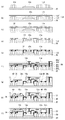
(第1の実施の形態)
図1は、本発明の第1の実施の形態に係る半導体装置100の断面図である。以降の図において、同一の構成要素には同一の符号を付し、適宜説明を省略する。
半導体装置100は、基材20、半導体チップ10a、10b、チップ部品12a、12b、絶縁基材30、配線パターン34、ビアプラグ32、外部引出電極36、凹部40、樹脂50を含む。図1において、便宜上、基材20の設けられた面を下方向とし、凹部40が設けられた面を上方向とする。
(First embodiment)
FIG. 1 is a cross-sectional view of a
The
基材20上には絶縁基材30が形成され、絶縁基材30内部には半導体チップ10a、10b、チップ部品12a、12bが埋め込まれ、配線パターン34およびビアプラグ32により互いに接続されることによって電子回路を形成している。
An
絶縁基材30は、多層構造を有しており、複数の絶縁体層30a〜30eを積層して形成される。これらの絶縁体層は同一材料により構成されていても良いし、それぞれ異なった材料により構成されていてもよい。絶縁体層30a〜30eの間には配線導体層が設けられ、配線パターン34が形成されている。配線パターン34は、各素子間を接続する配線としての他、インダクタやコンデンサとして形成していてもよい。
The insulating
半導体チップ10a、10bは、例えばトランジスタ、ダイオードや受動素子が集積化されたICチップ等であり、シリコンやシリコンゲルマニウム、ガリウムヒ素等の半導体上に形成される集積回路である。チップ部品12a、12bは、具体的には、コンデンサ、インダクタ、抵抗器などである。半導体チップ10aおよびチップ部品12aは、基材20にマウントされて絶縁体層30aに埋め込まれている。
The
ビアプラグ32は、異なる配線導体層の配線パターン34を電気的に接続するために設けられている。さらに、絶縁体層30aに埋め込まれた半導体チップ10a、チップ部品12aは、このビアプラグ32によって配線パターン34と電気的に接続される。
The via
絶縁基材30の上面には凹部40が形成されている。この凹部40は、その底部が、いずれかの配線導体層となるように形成されており、半導体装置100を上方向からみると、底部には配線パターン34が露出している。半導体チップ10bおよびチップ部品12bは、この露出した配線パターン34に対してダイボンド、ワイヤボンドされ、またはハンダにより実装されて、それぞれ配線パターン34と物理的、電気的に接続される。凹部40は樹脂50によって封止されている。
A
外部引出電極36は、半導体装置100の上面に設けられており、外部から電源の供給を受け、または信号の入出力を行うI/O端子として機能する。外部引出電極36は、半導体装置100の下面に設けられていてもよい。この場合には、基材20にビアプラグを設けて、下面に信号線を引き出せばよい。
The
本実施の形態に係る半導体装置100によれば、半導体装置100の表面に凹部40を形成することにより、各種部品の実装面を追加でき、より高密度な部品実装が実現することができる。
この凹部40に実装された半導体チップ10bは、樹脂50による封止工程前であれば内部に形成される抵抗、コンデンサのトリミングを行うことができる。従って、半導体装置100の組み立て後においても、回路特性の調整を行うことができ、歩留まりの向上を図ることができる。
According to
The
また、凹部40にチップ抵抗やチップコンデンサ等のチップ部品12bを実装した場合、樹脂50による封止工程前であれば、チップ部品12b載せ替えることによって回路定数を変更することができ、回路特性の向上、歩留まりの改善等を図ることができる。
さらに、絶縁基材30内の配線導体層に形成された配線パターン34が凹部40から露出している場合には、この配線パターンをトリミングすることによっても回路定数を変更することができる。
Further, when the
Furthermore, when the
また、半導体チップから発生する熱の一部は、外部引出電極36を介して外部へと放熱される。従って、本実施の形態のように、凹部40を、外部引出電極36の形成される面と同一の面に形成した場合には、発熱の多い半導体チップをその凹部に実装することにより、半導体チップと外部電極との距離が近くなるため、放熱の面で有利となる。この効果は、特に絶縁体層に熱伝導率の低い材料を用いた場合に顕著となる。
A part of the heat generated from the semiconductor chip is radiated to the outside through the
次に、本実施の形態に係る半導体装置100の製造方法について説明する。図2(a)〜(i)は、図1の半導体装置100の製造工程を示す工程断面図である。
Next, a method for manufacturing the
まず、図2(a)に示すように、基材20上に複数の半導体チップ10aやチップ部品12a等の回路素子を固定するダイ・チップボンド工程を行う。ここで、基材20は接着性を有し、半導体チップ10aおよびチップ部品12aを表面に固定することのできるテープ基材としてもよい。基材20の材料としては、樹脂フィルムや、アルミニウム板などの伝熱性材料を用いることもできる。また、後述するエポキシ樹脂、BTレジン等のメラミン誘導体、液晶ポリマー、PPE樹脂、ポリイミド樹脂、フッ素樹脂、フェノール樹脂、ポリアミドビスマレイミド等の有機物を用いてもよい。
First, as shown in FIG. 2A, a die / chip bonding process is performed in which circuit elements such as a plurality of
また、本実施の形態において、基材20として、伸縮可能な材料を用いることもできる。このような材料として、例えばPETフィルムを用いることができる。あるいは、基材20として、UV光反応性フィルムを用いることもできる。UV光反応性フィルムとしては、例えば半導体(チップ)をカットする際の支持体として使用される粘着テープであって、紫外線照射により、粘着力が変換するタイプの粘着テープが市販されている。
In the present embodiment, a stretchable material can also be used as the
基材20として、伸縮可能な材料を用いる場合には、基材20を図中横方向に伸張させた後に、基材20上に複数の半導体チップ10aおよびチップ部品12aを固定する。
When a stretchable material is used as the
続いて、図2(b)に示すように、絶縁性樹脂膜122上に導電性膜120が貼付された導電性膜付き絶縁性樹脂膜124を基材20上に貼付し、真空プレスにより、基材20と導電性膜付き絶縁性樹脂膜124を圧着させる。導電性膜付き絶縁性樹脂膜124は、例えば、銅箔付き樹脂膜である。
その結果、半導体チップ10aおよびチップ部品12aは絶縁性樹脂膜122内に押しまれる。導電性膜120は、配線導体層となり、後の工程により配線パターンが形成される。
Subsequently, as shown in FIG. 2 (b), an insulating
As a result, the
本実施の形態において、半導体チップ10aおよびチップ部品12aが固定された基材20を伸張させた状態で半導体チップ10aおよびチップ部品12aを絶縁性樹脂膜122内に押し込む場合、絶縁性樹脂膜122内に半導体チップ10aおよびチップ部品12aを押し込む際に、素子間の間隔が広くなり、素子間に絶縁性樹脂膜122が押し込まれやすくなる。そのため、半導体チップ10aおよびチップ部品12aと絶縁性樹脂膜122との密着性を良好にすることができる。
逆に、基材20を収縮させた状態で半導体チップ10aおよびチップ部品12aを絶縁性樹脂膜122内に押し込む場合には、素子間の間隔が狭くなるため、高密度な素子配置が可能となる。
In the present embodiment, when the
On the other hand, when the
また、複数の半導体チップ10aおよびチップ部品12aに段差が生じている場合でも、半導体チップ10aおよびチップ部品12a上に絶縁性樹脂膜が入り込むため、基材20から導電性膜120までの厚みを均一に保つこともできる。これにより、半導体装置100の寸法精度を高めることができる。
Even when there are steps in the plurality of
導電性膜120は、例えば圧延銅箔等の圧延金属である。絶縁性樹脂膜122としては、加熱することにより軟化する材料であればどのようなものを用いることもできるが、例えばエポキシ樹脂、BTレジン等のメラミン誘導体、液晶ポリマー、PPE樹脂、ポリイミド樹脂、フッ素樹脂、フェノール樹脂、ポリアミドビスマレイミド等の有機物を用いることができる。このような材料を用いることにより、回路装置の剛性を高めることができ、回路装置の安定性を向上することができる。
The
エポキシ樹脂としては、メラミン、メラミンシアヌレート、メチロール化メラミン、(イソ)シアヌール酸、メラム、メレム、メロン、サクシノグアミン、硫酸メラミン、硫酸アセトグアナミン、硫酸メラム、硫酸グアニルメラミン、メラミン樹脂、BTレジン、シアヌール酸、イソシアヌール酸、イソシアヌール酸誘導体、メラミンイソシアヌレート、ベンゾグアナミン、アセトグアナミン等のメラミン誘導体、グアニジン系化合物等が例示される。 Epoxy resins include melamine, melamine cyanurate, methylolated melamine, (iso) cyanuric acid, melam, melem, melon, succinoguanamine, melamine sulfate, acetoguanamine sulfate, melam sulfate, guanyl melamine sulfate, melamine resin, BT resin, cyanur Examples thereof include melamine derivatives such as acid, isocyanuric acid, isocyanuric acid derivatives, melamine isocyanurate, benzoguanamine and acetoguanamine, and guanidine compounds.
液晶ポリマーとしては、芳香族系液晶ポリエステル、ポリイミド、ポリエステルアミドや、それらを包含する樹脂組成物が例示される。このうち、耐熱性、加工性およぼ吸湿性のバランスに優れる液晶ポリエステルまたは液晶ポリエステルを含有する組成物が好ましい。 Examples of the liquid crystal polymer include aromatic liquid crystal polyester, polyimide, polyester amide, and a resin composition containing them. Among these, a liquid crystal polyester or a composition containing a liquid crystal polyester having a good balance of heat resistance, workability and hygroscopicity is preferable.
液晶ポリエステルとしては、例えば、(1)芳香族ジカルボン酸と芳香族ジオールと芳香族ヒドロキシカルボン酸とを反応させて得られるもの、(2)異種の芳香族ヒドロキシカルボン酸の組み合わせを反応させて得られるもの、(3)芳香族ジカルボン酸と芳香族ジオールとを反応させて得られるもの、(4)ポリエチレンテレフタレート等のポリエステルに芳香族ヒドロキシカルボン酸を反応させて得られるもの、等があげられる。なお、これらの芳香族ジカルボン酸、芳香族ジオールおよび芳香族ヒドロキシカルボン酸の代わりにそれらのエステル誘導体が使用されることもある。さらに、これらの芳香族ジカルボン酸、芳香族ジオールおよび芳香族ヒドロキシカルボン酸は芳香族部分がハロゲン原子、アルキル基、アリール基等で置換されたものが使用されることもある。 Examples of liquid crystal polyesters include (1) those obtained by reacting aromatic dicarboxylic acids, aromatic diols and aromatic hydroxycarboxylic acids, and (2) obtained by reacting combinations of different types of aromatic hydroxycarboxylic acids. (3) those obtained by reacting an aromatic dicarboxylic acid and an aromatic diol, and (4) those obtained by reacting an aromatic hydroxycarboxylic acid with a polyester such as polyethylene terephthalate. In addition, those ester derivatives may be used in place of these aromatic dicarboxylic acids, aromatic diols and aromatic hydroxycarboxylic acids. Further, these aromatic dicarboxylic acids, aromatic diols and aromatic hydroxycarboxylic acids may be used in which the aromatic moiety is substituted with a halogen atom, an alkyl group, an aryl group or the like.
また、絶縁性樹脂膜122には、フィラーまたは繊維等の充填材を含めることができる。フィラーとしては、例えば粒子状または繊維状のSiO2やSiNを用いることができる。絶縁性樹脂膜122にフィラーや繊維を含めることにより、絶縁性樹脂膜122を加熱して半導体チップ10aおよびチップ部品12aを熱圧着した後、絶縁性樹脂膜122を例えば室温に冷却する際に、絶縁性樹脂膜122の反りを低減することができ、また熱伝導性も向上する。これにより、半導体チップ10aおよびチップ部品12aと絶縁性樹脂膜122との密着性を高めることができる。また、絶縁性樹脂膜122に繊維を含めた場合、絶縁性樹脂膜122の剛性を高めることができ、ハンドリングが容易になる。このような観点からは、絶縁性樹脂膜122を構成する材料としてアラミド不織布を用いると、繊維よりも樹脂の流動性が高くなるため、加工性を良好にすることができる。
The insulating
導電性膜付き絶縁性樹脂膜124としては、フィルム状の絶縁性樹脂膜122上に導電性膜120が付着したものを用いることができる。また、導電性膜付き絶縁性樹脂膜124は、導電性膜120上に絶縁性樹脂膜122を構成する樹脂組成物を塗布、乾燥することにより形成することもできる。本実施の形態において、樹脂組成物は、本発明の目的に反しない範囲において、硬化剤、硬化促進剤、その他の成分を含むことができる。導電性膜付き絶縁性樹脂膜124は、絶縁性樹脂膜122がBステージ化(一次硬化、半硬化あるいは仮硬化した状態を意味する)した状態で基材20上に配置される。
As the insulating
このようにすれば、絶縁性樹脂膜122と半導体チップ10aおよびチップ部品12aとの密着性を高めることができる。この後、絶縁性樹脂膜122を構成する樹脂の種類に応じて絶縁性樹脂膜122を加熱し、真空下または減圧下で導電性膜付き絶縁性樹脂膜124と半導体チップ10aおよびチップ部品12aを圧着する。また、他の例において、フィルム状の絶縁性樹脂膜122をBステージ化した状態で基材20上に配置し、さらにその上に導電性膜120を配置して絶縁性樹脂膜122を半導体チップ10aおよびチップ部品12aと熱圧着する際に、導電性膜120を絶縁性樹脂膜122に熱圧着することによっても導電性膜付き絶縁性樹脂膜124を形成することができる。
In this way, the adhesion between the insulating
そして、図2(c)に示すように、導電性膜120を、レーザー直描法(トレパニングアライメント)またはウェット銅エッチングにより配線形成する配線パターニング工程を行い、配線パターン34を形成する。
Then, as shown in FIG. 2C, the
また、この後、図2(d)に示すように、炭酸ガスレーザー、YAGレーザー、ドライエッチングを組み合わせて絶縁性樹脂膜122にビアホール(スルーホール)を形成するビアホール形成工程を行う。
Thereafter, as shown in FIG. 2D, a via hole forming step is performed in which a via hole (through hole) is formed in the insulating
続いて、図2(e)に示すように、高アスペクト比対応の無電解銅めっき、電解銅めっきにより、導電性膜を形成するとともに、スルーホール内を導電性材料で埋め込み、ビアプラグ32を形成するめっき工程を行う。
Subsequently, as shown in FIG. 2E, a conductive film is formed by electroless copper plating and electrolytic copper plating corresponding to a high aspect ratio, and the through hole is filled with a conductive material to form a via
ビアプラグ32は、より詳細には以下のように形成することができる。炭酸ガスレーザ、YAGレーザ、ドライエッチング等を組み合わせて絶縁体層にスルーホール128を形成する。次にスルーホール128内に、無電解銅めっきにより全面に0.5〜1μm程度の薄膜を形成した後、電解めっきにより約20μm程度の膜を形成する。無電解めっき用触媒は通常パラジウムを用いることが多く、可とう性の絶縁基材に無電解めっき触媒を付着させるには、パラジウムを錯体の状態で水溶液に含ませ、可とう性の絶縁基材を浸漬して表面にパラジウム錯体を付着させ、そのまま、還元剤を用いて金属パラジウムに還元することによって可とう性の絶縁基材表面にめっきを開始するための核を形成することができる。
More specifically, the via
ビアプラグ32内には適宜充填材料を埋め込んでもよい。充填材料としては絶縁性材料や導電性材料等種々のものを用いることができる。また、めっき等により、銅を充填材料として埋め込むこともできる。
A filling material may be appropriately embedded in the via
次いで、導電性膜付き絶縁性樹脂膜124を順次積層し、導電性膜120上に配線パターン34を形成し、ビアプラグ32で接続する工程を繰り返すことによって絶縁体層30a〜30eの積層された絶縁基材30が形成される(図2(f))。
Next, an insulating
次に、図2(g)に示すように絶縁基材30の上面に凹部40を設ける。凹部40は、ドリルを用いて機械的に加工する他、レーザ加工、あるいはエッチングとこれらの組み合わせによって形成することができる。凹部40の深さは、何れかの配線導体層までとし、その配線導体層に形成された配線パターン34bを露出させる。
Next, as shown in FIG. 2G, a
次いで、凹部40の内部に半導体チップ10b、チップ部品12bを実装する。半導体チップ10bは銀ペーストなどによってダイボンディングを行い、金線などによりワイヤボンディングすることにより物理的、電気的に配線パターン34bと接続する。また、チップ部品12bはハンダにより配線パターン34bと物理的、電気的に接続される。
Next, the
次いで、図示しない外部引出電極を形成し、必要に応じて検査工程を行う。この検査の結果、所望の特性が得られていなければ、半導体チップ10bのトリミングや、チップ部品12bの変更等を行ってもよい。
Next, an external extraction electrode (not shown) is formed, and an inspection process is performed as necessary. If the desired characteristics are not obtained as a result of this inspection, the
その後、凹部40に樹脂50をポッティングし、半導体チップ10bおよびチップ部品12bを封止する。
以上の工程を経て、第1の実施の形態に係る半導体装置100を製造することができる。
Thereafter, the
Through the above steps, the
(第2の実施の形態)
第2の実施の形態に係る半導体装置200について、上述の半導体装置100との相違点を中心に説明する。図3は、第2の実施の形態に係る半導体装置200の断面図である。
半導体装置200は、基材20、半導体チップ10a、チップ部品12a、絶縁基材30、配線パターン34、ビアプラグ32、外部引出電極36を含む。図3においても、便宜上、基材20を下方向とし、外部引出電極36が設けられた面を上方向とする。
(Second Embodiment)
A
The
絶縁基材30は、多層構造を有しており、複数の絶縁体層30a〜30eを積層して形成される。基材20と隣接する絶縁体層30aに半導体チップ10a、チップ部品12aが埋め込まれており、ビアプラグ32および配線パターン34により各部材が接続されて回路を構成している点では図1の半導体装置100と同様である。
The insulating
図3の半導体装置200には、半導体チップ10a、チップ部品12aの間隙部、すなわち周辺のスペースに配線パターン34cが設けられている。
通常の半導体チップ10aの厚みは100〜300μmであり、抵抗やコンデンサ等のチップ部品12aの高さはいわゆる0603サイズで300μm、1005サイズで500μm程度である。本実施の形態では、半導体チップ10a等が実装されていない間隙部にも、配線導体層を形成して、より高密度な配線を行っている。
In the
The thickness of the
この半導体装置200によれば、半導体チップやチップ部品の周辺のスペースを有効利用することにより、高密度な配線を実現することができ、配線の引き回しの自由度を高めることができる。
According to the
第2の実施の形態に係る半導体装置200の製造方法について説明する。図4(a)〜(h)は、図3に示した半導体装置200の製造工程の一部を示す工程断面図である。
A method for manufacturing the
図4(a)は、基材20に半導体チップ10a、チップ部品12aがダイボンディング、チップボンディングされ、絶縁性樹脂膜122に埋め込まれた状態を示している。ここまでは、図2(a)〜(b)に示す工程により行うことができる。絶縁性樹脂膜122には、導電性膜120が貼られていてもいなくてもよい。
FIG. 4A shows a state in which the
続いて、図4(b)に示すように、絶縁性樹脂膜122に開口部150を形成する。開口部150の形成は、半導体チップ10a、チップ部品12aの間隙部であって、図3の配線パターン34cを形成したい箇所に対して行う。開口部150は、例えばドリル、レーザ加工、あるいはエッチングとこれらの組み合わせにより形成される。
Subsequently, as illustrated in FIG. 4B, an
図4(c)では、上記工程により絶縁性樹脂膜122に形成された開口部150に絶縁体層130aを形成する。この絶縁体層130aは、樹脂ポッティング等により形成することができる。ポッティングする樹脂としては、絶縁性樹脂膜122と同様、加熱することにより軟化するエポキシ樹脂、BTレジン等のメラミン誘導体、液晶ポリマー、PPE樹脂、ポリイミド樹脂、フッ素樹脂、フェノール樹脂、ポリアミドビスマレイミド等の有機物を用いることができる。
In FIG. 4C, the
次いで図4(d)に示すように、絶縁体層130a上に、配線パターン34cを形成する。配線パターン34cは、例えば無電解めっき法およびエッチングを組み合わせることにより形成することができる。同様にして図4(e)に示すように再度樹脂ポッティングにより絶縁体層130bを積層し、その上に配線パターン34cを形成する。
Next, as shown in FIG. 4D, a
次いで図4(f)に示すように絶縁体層130bにレーザ照射等によりビアホールを形成し、ビアプラグ32により配線パターン34c間を電気的に接続する(図4(g))。
Next, as shown in FIG. 4F, via holes are formed in the insulating
その後、樹脂ポッティングにより絶縁体層130cを形成することにより、絶縁性樹脂膜122中に、複数の配線導体層が形成される。以降の工程は図2と同様に行えばよい。なお、絶縁体層130cは、図4(g)に示す状態において、半導体装置200全体に上から絶縁性樹脂膜をプレスすることにより形成してもよい。
Thereafter, the insulating
以上の製造方法により、複数の半導体チップ10aまたはチップ部品12a間の間隙部に配線パターンを形成することができ、半導体装置200内のスペースを有効利用し、より高密度配線を実現することができる。
According to the above manufacturing method, a wiring pattern can be formed in a gap between a plurality of
図4(a)〜(b)に示す工程は、図5(a)〜(c)に示す工程により行うこともできる。図5(a)において、半導体チップ10a、チップ部品12aを基材20にダイ、チップボンディングする。次に、絶縁性樹脂膜122に予め開口部150を設けておき、図5(b)、(c)に示すように、この絶縁性樹脂膜122を基材20上に貼付し、真空プレスにより、半導体チップ10aおよびチップ部品12aを絶縁性樹脂膜122内に押し込む。
絶縁性樹脂膜122の開口部150は、配線パターン34cを形成する箇所に設けられる。
The steps shown in FIGS. 4A to 4B can also be performed by the steps shown in FIGS. 5A to 5C. In FIG. 5A, the
The
また、図6(a)〜(f)に示す工程によっても配線パターン34cを形成することができる。
まず、図6(a)に示すように、基材20に半導体チップ10aおよびチップ部品12aをダイ、チップボンディングする。次いで、図6(b)に示すように、配線パターン34cを形成したい箇所に局所的に樹脂ポッティングを行い、絶縁体層130aを形成する。続いて図6(c)〜(e)に示すように配線パターン34c、絶縁体層130bの形成し、ビアプラグ32を形成する。
Also, the
First, as shown in FIG. 6A, the
続いて図6(f)に示すように、絶縁性樹脂膜122を基材20上に貼付し、真空プレスにより、半導体チップ10aおよびチップ部品12aを絶縁性樹脂膜122内に押し込む。
Subsequently, as shown in FIG. 6F, the insulating
以上のようにしても、複数の半導体チップ10aまたはチップ部品12a間の間隙部に配線パターン34cを形成することができ、半導体装置200内のスペースを有効利用した高密度配線を実現することができる。
Even in the above manner, the
本発明は、上述の各実施の形態に限定されるものではなく、当業者の知識に基づいて各種の設計変更等の変形を加えることも可能であり、そのような変形が加えられた実施の形態も本発明の範囲に含まれうるものである。 The present invention is not limited to the above-described embodiments, and various modifications such as design changes can be added based on the knowledge of those skilled in the art. The form can also be included in the scope of the present invention.
実施の形態では、半導体チップとチップ部品が混載される半導体装置について説明したがこれには限られず、半導体チップが実装される様々な半導体装置に適用することができる。 In the embodiment, the semiconductor device in which the semiconductor chip and the chip component are mixedly described has been described. However, the present invention is not limited to this and can be applied to various semiconductor devices on which the semiconductor chip is mounted.
また、第1の実施の形態において、一つの凹部40には、半導体チップや、チップ部品などの単一の回路素子が実装されていてもよいし、複数の回路素子が実装されていてもよい。これらは、凹部のサイズに応じて適宜決定すればよい。
In the first embodiment, a single circuit element such as a semiconductor chip or a chip component may be mounted in one
なお、上記実施の形態においては、基材20上に半導体チップ10およびチップ部品12が実装されているが、銅などによる配線パターンを持ちながら半導体回路素子を支持するためのコアを使用しないコアレスSIP(System In Package)として知られるISB(Integrated System in Board:登録商標)についても本発明が適用され得る。
In the above-described embodiment, the semiconductor chip 10 and the chip component 12 are mounted on the
10 半導体チップ、 12 チップ部品、 20 基材、 30 絶縁基材、 32 ビアプラグ、 34 配線パターン、 36 外部引出電極、 40 凹部、 50 樹脂、 100 半導体装置、 120 導電性膜、 122 絶縁性樹脂膜、 124 導電性膜付き絶縁性樹脂膜、 200 半導体装置。 DESCRIPTION OF SYMBOLS 10 Semiconductor chip, 12 Chip components, 20 Base material, 30 Insulation base material, 32 Via plug, 34 Wiring pattern, 36 External extraction electrode, 40 Recessed part, 50 Resin, 100 Semiconductor device, 120 Conductive film, 122 Insulating resin film, 124 Insulating resin film with conductive film, 200 Semiconductor device.
Claims (4)
前記基材上に、前記複数の回路素子が埋め込まれた第1の絶縁樹脂膜と、
前記基材からの厚みが均一になるように前記第1の絶縁樹脂膜上に配置された導電性膜からなり、前記複数の回路素子を互いに接続する第1の配線導体層と、
前記第1の絶縁樹脂膜及び前記第1の配線導体層上に、前記第1の絶縁樹脂膜よりも膜厚の薄い第2の絶縁樹脂膜及び第2の配線導体層からなる積層体を複数備えた多層構造体と、
前記第2の絶縁樹脂膜に備えられ、前記第1又は第2の配線導体層に到達した凹部と、
前記凹部に実装され前記第1又は第2の配線導体層と接続された回路素子と、を備えることを特徴とする回路装置。 A substrate on which a plurality of circuit elements having different heights are fixed;
A first insulating resin film in which the plurality of circuit elements are embedded on the substrate;
A first wiring conductor layer comprising a conductive film disposed on the first insulating resin film so as to have a uniform thickness from the substrate, and connecting the plurality of circuit elements to each other;
On the first insulating resin film and the first wiring conductor layer, a plurality of laminates composed of a second insulating resin film and a second wiring conductor layer that are thinner than the first insulating resin film are formed. A multilayer structure with
A concave portion provided in the second insulating resin film and reaching the first or second wiring conductor layer;
Circuit device characterized by and a circuit element connected to the first or the second wiring conductor layers are mounted in the recess.
第1の絶縁樹脂膜上に導電性膜を配置し、前記導電性膜に加圧して前記第1の絶縁樹脂膜側を前記基材に圧着することにより、前記複数の回路素子を前記第1の絶縁樹脂膜内に埋め込む工程と、
前記導電性膜をパターニングして第1の配線パターンを形成する工程と、
前記第1の絶縁樹脂膜に設けたビアプラグと、前記第1の配線パターンとにより前記複数の回路素子を互いに接続する工程と、
前記第1の絶縁樹脂膜及び前記第1の配線パターン上に、前記第1の絶縁樹脂膜よりも膜厚の薄い第2の絶縁樹脂膜及び第2の配線パターンを複数層備えた多層構造体を形成する工程と、
前記第2の絶縁樹脂膜に、前記第1又は第2の配線パターンが露出する凹部を形成する工程と、
を含むことを特徴とする回路装置の製造方法。 Preparing a substrate on which a plurality of circuit elements having different heights are fixed;
A conductive film is disposed on the first insulating resin film, and the plurality of circuit elements are connected to the first by pressing the conductive film and pressure-bonding the first insulating resin film side to the substrate. Embedded in the insulating resin film,
Patterning the conductive film to form a first wiring pattern;
Connecting the plurality of circuit elements to each other by a via plug provided in the first insulating resin film and the first wiring pattern;
A multilayer structure including a plurality of second insulating resin films and second wiring patterns having a thickness smaller than that of the first insulating resin film on the first insulating resin film and the first wiring pattern. Forming a step;
Forming a recess exposing the first or second wiring pattern in the second insulating resin film;
A method for manufacturing a circuit device , comprising:
Priority Applications (3)
| Application Number | Priority Date | Filing Date | Title |
|---|---|---|---|
| JP2004253998A JP4252019B2 (en) | 2004-09-01 | 2004-09-01 | Circuit device and manufacturing method thereof |
| US11/215,121 US7875980B2 (en) | 2004-09-01 | 2005-08-31 | Semiconductor device having laminated structure |
| CN2005100980208A CN1744314B (en) | 2004-09-01 | 2005-09-01 | Semiconductor device having laminated structure and manufacturing method |
Applications Claiming Priority (1)
| Application Number | Priority Date | Filing Date | Title |
|---|---|---|---|
| JP2004253998A JP4252019B2 (en) | 2004-09-01 | 2004-09-01 | Circuit device and manufacturing method thereof |
Related Child Applications (1)
| Application Number | Title | Priority Date | Filing Date |
|---|---|---|---|
| JP2008228563A Division JP2009033185A (en) | 2008-09-05 | 2008-09-05 | Semiconductor device and its production method |
Publications (2)
| Publication Number | Publication Date |
|---|---|
| JP2006073702A JP2006073702A (en) | 2006-03-16 |
| JP4252019B2 true JP4252019B2 (en) | 2009-04-08 |
Family
ID=35941943
Family Applications (1)
| Application Number | Title | Priority Date | Filing Date |
|---|---|---|---|
| JP2004253998A Expired - Fee Related JP4252019B2 (en) | 2004-09-01 | 2004-09-01 | Circuit device and manufacturing method thereof |
Country Status (3)
| Country | Link |
|---|---|
| US (1) | US7875980B2 (en) |
| JP (1) | JP4252019B2 (en) |
| CN (1) | CN1744314B (en) |
Families Citing this family (15)
| Publication number | Priority date | Publication date | Assignee | Title |
|---|---|---|---|---|
| US20090057903A1 (en) * | 2007-03-29 | 2009-03-05 | Yoshio Okayama | Semiconductor module, method for manufacturing semiconductor modules, semiconductor apparatus, method for manufacturing semiconductor apparatuses, and portable device |
| JP2008300560A (en) * | 2007-05-30 | 2008-12-11 | Sony Corp | Semiconductor device, and manufacturing method thereof |
| KR100945285B1 (en) * | 2007-09-18 | 2010-03-03 | 삼성전기주식회사 | Electronic components embedded PCB and method for manufacturing thereof |
| US8963341B2 (en) * | 2007-10-16 | 2015-02-24 | Edward Binkley | Process for placing, securing and interconnecting electronic components |
| US20110156261A1 (en) * | 2009-03-24 | 2011-06-30 | Christopher James Kapusta | Integrated circuit package and method of making same |
| US9299661B2 (en) * | 2009-03-24 | 2016-03-29 | General Electric Company | Integrated circuit package and method of making same |
| US20140000099A1 (en) * | 2012-06-29 | 2014-01-02 | Noah Austin Spivak | Methods for building resistive elements into printed circuit boards |
| JP2014116548A (en) * | 2012-12-12 | 2014-06-26 | Ngk Spark Plug Co Ltd | Multilayer wiring board and manufacturing method therefor |
| US9185794B1 (en) * | 2013-07-31 | 2015-11-10 | Juniper Networks, Inc. | Apparatus and methods for placement of discrete components on internal printed circuit board layers |
| EP2881753B1 (en) | 2013-12-05 | 2019-03-06 | ams AG | Optical sensor arrangement and method of producing an optical sensor arrangement |
| EP2881983B1 (en) | 2013-12-05 | 2019-09-18 | ams AG | Interposer-chip-arrangement for dense packaging of chips |
| CN105848416B (en) * | 2016-03-31 | 2019-04-26 | 华为技术有限公司 | A kind of substrate and mobile terminal |
| WO2018079278A1 (en) * | 2016-10-25 | 2018-05-03 | 株式会社村田製作所 | Circuit module |
| US10541153B2 (en) * | 2017-08-03 | 2020-01-21 | General Electric Company | Electronics package with integrated interconnect structure and method of manufacturing thereof |
| CN114270714B (en) * | 2019-08-28 | 2024-01-05 | 株式会社村田制作所 | High-frequency module and communication device |
Family Cites Families (14)
| Publication number | Priority date | Publication date | Assignee | Title |
|---|---|---|---|---|
| JPS6375075A (en) | 1986-09-18 | 1988-04-05 | Toyo Seikan Kaisha Ltd | Water based coating material for can and coated can body |
| JPH065993A (en) | 1992-06-17 | 1994-01-14 | Tanaka Kikinzoku Kogyo Kk | Multilayer board with internal layer circuits exposed |
| JPH08162486A (en) | 1994-12-05 | 1996-06-21 | Shin Etsu Chem Co Ltd | Resin-sealing of semiconductor element |
| JP2701802B2 (en) * | 1995-07-17 | 1998-01-21 | 日本電気株式会社 | Printed circuit board for bare chip mounting |
| JPH09162320A (en) * | 1995-12-08 | 1997-06-20 | Shinko Electric Ind Co Ltd | Semiconductor package and semiconductor device |
| US6038133A (en) * | 1997-11-25 | 2000-03-14 | Matsushita Electric Industrial Co., Ltd. | Circuit component built-in module and method for producing the same |
| DE10122705B4 (en) * | 2000-05-11 | 2012-07-26 | Mitutoyo Corp. | Device with functional component and method for its production |
| JP4529262B2 (en) | 2000-09-14 | 2010-08-25 | ソニー株式会社 | High frequency module device and manufacturing method thereof |
| JP2003142797A (en) | 2001-11-02 | 2003-05-16 | Matsushita Electric Ind Co Ltd | Finished product with electronic component mounted and manufacturing method thereof |
| TWI234253B (en) * | 2002-05-31 | 2005-06-11 | Fujitsu Ltd | Semiconductor device and manufacturing method thereof |
| JP3976089B2 (en) * | 2002-08-09 | 2007-09-12 | 株式会社リコー | Semiconductor integrated circuit device and manufacturing method thereof |
| JP4056854B2 (en) * | 2002-11-05 | 2008-03-05 | 新光電気工業株式会社 | Manufacturing method of semiconductor device |
| JP4228677B2 (en) * | 2002-12-06 | 2009-02-25 | パナソニック株式会社 | Circuit board |
| JP2004273591A (en) * | 2003-03-06 | 2004-09-30 | Seiko Epson Corp | Semiconductor device and its fabricating process |
-
2004
- 2004-09-01 JP JP2004253998A patent/JP4252019B2/en not_active Expired - Fee Related
-
2005
- 2005-08-31 US US11/215,121 patent/US7875980B2/en not_active Expired - Fee Related
- 2005-09-01 CN CN2005100980208A patent/CN1744314B/en not_active Expired - Fee Related
Also Published As
| Publication number | Publication date |
|---|---|
| JP2006073702A (en) | 2006-03-16 |
| US20060043606A1 (en) | 2006-03-02 |
| US7875980B2 (en) | 2011-01-25 |
| CN1744314A (en) | 2006-03-08 |
| CN1744314B (en) | 2011-05-04 |
Similar Documents
| Publication | Publication Date | Title |
|---|---|---|
| US7875980B2 (en) | Semiconductor device having laminated structure | |
| US11222852B2 (en) | Method for fabricating electronic package | |
| US10141203B2 (en) | Electrical interconnect structure for an embedded electronics package | |
| US7683268B2 (en) | Semiconductor module with high process accuracy, manufacturing method thereof, and semiconductor device therewith | |
| JP4688679B2 (en) | Semiconductor module | |
| US20110133341A1 (en) | Semiconductor package and method of manufacturing the same | |
| US10098243B2 (en) | Printed wiring board and semiconductor package | |
| JP2003500832A (en) | High density electronic package and method of manufacturing the same | |
| JP4875925B2 (en) | Multilayer wiring board and manufacturing method thereof | |
| CN100380653C (en) | Semiconductor device and method of manufacturing semiconductor device | |
| US8093699B2 (en) | Circuit device with circuit board and semiconductor chip mounted thereon | |
| KR101109356B1 (en) | Method for manufacturing the embedded printed circuit board | |
| US20060193108A1 (en) | Circuit device and manufacturing method thereof | |
| US9299661B2 (en) | Integrated circuit package and method of making same | |
| US10510638B2 (en) | Electronic component-embedded board | |
| US20240164021A1 (en) | Embedded component package structure and manufacturing method thereof | |
| JP2009033185A (en) | Semiconductor device and its production method | |
| KR20150043135A (en) | printed circuit board which includes metal layer and semiconductor package including the same | |
| US11445617B2 (en) | Package structure and manufacturing method thereof | |
| JP2005109037A (en) | Semiconductor device | |
| US20240112978A1 (en) | Electronic package | |
| JP2003163240A (en) | Semiconductor device and manufacturing method therefor | |
| JP2005109068A (en) | Semiconductor device and manufacturing method thereof | |
| CN117998729A (en) | Embedded device packaging substrate and manufacturing method thereof | |
| KR20180092379A (en) | Power electronics package and method of manufacturing thereof |
Legal Events
| Date | Code | Title | Description |
|---|---|---|---|
| A621 | Written request for application examination |
Free format text: JAPANESE INTERMEDIATE CODE: A621 Effective date: 20061012 |
|
| A977 | Report on retrieval |
Free format text: JAPANESE INTERMEDIATE CODE: A971007 Effective date: 20080704 |
|
| A131 | Notification of reasons for refusal |
Free format text: JAPANESE INTERMEDIATE CODE: A131 Effective date: 20080708 |
|
| A521 | Request for written amendment filed |
Free format text: JAPANESE INTERMEDIATE CODE: A523 Effective date: 20080908 |
|
| A131 | Notification of reasons for refusal |
Free format text: JAPANESE INTERMEDIATE CODE: A131 Effective date: 20080930 |
|
| A521 | Request for written amendment filed |
Free format text: JAPANESE INTERMEDIATE CODE: A523 Effective date: 20081201 |
|
| TRDD | Decision of grant or rejection written | ||
| A01 | Written decision to grant a patent or to grant a registration (utility model) |
Free format text: JAPANESE INTERMEDIATE CODE: A01 Effective date: 20081224 |
|
| A01 | Written decision to grant a patent or to grant a registration (utility model) |
Free format text: JAPANESE INTERMEDIATE CODE: A01 |
|
| A61 | First payment of annual fees (during grant procedure) |
Free format text: JAPANESE INTERMEDIATE CODE: A61 Effective date: 20090120 |
|
| FPAY | Renewal fee payment (event date is renewal date of database) |
Free format text: PAYMENT UNTIL: 20120130 Year of fee payment: 3 |
|
| FPAY | Renewal fee payment (event date is renewal date of database) |
Free format text: PAYMENT UNTIL: 20130130 Year of fee payment: 4 |
|
| FPAY | Renewal fee payment (event date is renewal date of database) |
Free format text: PAYMENT UNTIL: 20140130 Year of fee payment: 5 |
|
| LAPS | Cancellation because of no payment of annual fees |