JP4249428B2 - Signal detection apparatus and detection method - Google Patents
Signal detection apparatus and detection method Download PDFInfo
- Publication number
- JP4249428B2 JP4249428B2 JP2002101445A JP2002101445A JP4249428B2 JP 4249428 B2 JP4249428 B2 JP 4249428B2 JP 2002101445 A JP2002101445 A JP 2002101445A JP 2002101445 A JP2002101445 A JP 2002101445A JP 4249428 B2 JP4249428 B2 JP 4249428B2
- Authority
- JP
- Japan
- Prior art keywords
- representation
- auxiliary
- signal
- frequency
- main
- Prior art date
- Legal status (The legal status is an assumption and is not a legal conclusion. Google has not performed a legal analysis and makes no representation as to the accuracy of the status listed.)
- Expired - Fee Related
Links
- 238000001514 detection method Methods 0.000 title description 10
- 238000000034 method Methods 0.000 claims description 29
- 230000004044 response Effects 0.000 claims description 29
- 230000014509 gene expression Effects 0.000 claims description 28
- 239000002131 composite material Substances 0.000 claims description 7
- 230000005540 biological transmission Effects 0.000 claims description 5
- 230000000295 complement effect Effects 0.000 claims description 4
- 230000001131 transforming effect Effects 0.000 claims 4
- 230000001419 dependent effect Effects 0.000 claims 1
- 230000001939 inductive effect Effects 0.000 claims 1
- 230000002194 synthesizing effect Effects 0.000 claims 1
- 238000010586 diagram Methods 0.000 description 18
- 238000005314 correlation function Methods 0.000 description 10
- 230000006870 function Effects 0.000 description 10
- 238000012545 processing Methods 0.000 description 9
- 230000015654 memory Effects 0.000 description 8
- 230000001788 irregular Effects 0.000 description 6
- 230000008901 benefit Effects 0.000 description 4
- 230000000737 periodic effect Effects 0.000 description 4
- 230000001934 delay Effects 0.000 description 3
- 230000010363 phase shift Effects 0.000 description 3
- 238000001228 spectrum Methods 0.000 description 3
- 230000001360 synchronised effect Effects 0.000 description 3
- 230000008859 change Effects 0.000 description 2
- 230000001427 coherent effect Effects 0.000 description 2
- 238000004891 communication Methods 0.000 description 2
- 230000003111 delayed effect Effects 0.000 description 2
- 230000033001 locomotion Effects 0.000 description 2
- 230000008569 process Effects 0.000 description 2
- 238000010183 spectrum analysis Methods 0.000 description 2
- 230000007704 transition Effects 0.000 description 2
- 238000012935 Averaging Methods 0.000 description 1
- 208000028964 Congenital reticular ichthyosiform erythroderma Diseases 0.000 description 1
- 108010076504 Protein Sorting Signals Proteins 0.000 description 1
- 230000002238 attenuated effect Effects 0.000 description 1
- 230000000694 effects Effects 0.000 description 1
- 230000010354 integration Effects 0.000 description 1
- 230000002452 interceptive effect Effects 0.000 description 1
- 238000005259 measurement Methods 0.000 description 1
- 238000005457 optimization Methods 0.000 description 1
- 238000003672 processing method Methods 0.000 description 1
- 230000005855 radiation Effects 0.000 description 1
Images


Classifications
-
- G—PHYSICS
- G01—MEASURING; TESTING
- G01S—RADIO DIRECTION-FINDING; RADIO NAVIGATION; DETERMINING DISTANCE OR VELOCITY BY USE OF RADIO WAVES; LOCATING OR PRESENCE-DETECTING BY USE OF THE REFLECTION OR RERADIATION OF RADIO WAVES; ANALOGOUS ARRANGEMENTS USING OTHER WAVES
- G01S13/00—Systems using the reflection or reradiation of radio waves, e.g. radar systems; Analogous systems using reflection or reradiation of waves whose nature or wavelength is irrelevant or unspecified
- G01S13/02—Systems using reflection of radio waves, e.g. primary radar systems; Analogous systems
- G01S13/50—Systems of measurement based on relative movement of target
- G01S13/52—Discriminating between fixed and moving objects or between objects moving at different speeds
Description
【0001】
【発明の属する技術分野】
本発明は、信号を検出する方法と装置とに関する。本発明は、特に、通信および測距の目的で使用される変調された干渉信号、特に障害物検出または衝突回避システムで使用される不規則な、すなわち無秩序の波形によって変調された実質的な連続信号に影響を及ぼす未知のドップラー周波数シフトにさらされ易いシステムに適用可能であるが、これに限定されるものではない。
【0002】
【従来の技術】
このようなシステムは、マルチユーザ環境、およびしばしば敵対的な環境で動作するように設計されており、自動車の用途、産業用ロボット、および無人車両ナビゲーションを含む広範な用途を意図している。
【0003】
図1は、標準的なマイクロ波障害物検出システムのブロック図である。このシステムは必要なレンジ分解能をもたらす適宜の帯域幅を有する実質的に連続的な波形x(t)を生成する信号発生器1を備えている。波形x(t)は、確定的な(周期的または非周期的)、無秩序な、または純粋に不規則なものでよい。
【0004】
このシステムは、更に、必要な搬送波周波数を有する正弦信号を生成するマイクロ波発振器2と、搬送波信号の(振幅、位相、または周波数のような)1つ、または複数のパラメータを変調波形x(t)で変調する変調器3と、変形された搬送波信号を必要なレベルに増幅する出力増幅器(PA)4と、変調された搬送波信号を表す電磁波を障害物6の方向に放射するマイクロ波送信アンテナ(TA)5と、障害物6から反射した電磁波を受けるマイクロ波受信アンテナ(RA)7と、受信アンテナ(RA)7によって供給される信号を増幅する入力増幅器(IA)8と、発振器2によって供給された基準搬送波信号および、入力増幅器(IA)8によって供給された信号を統合して処理して、変調波形x(t)の時間遅延された複製y(t)を再構成するための干渉復調器9とを有している。
【0005】
次に、相関器のような適宜のプロセッサ10によって変調波形x(t)と、その時間遅延された複製y(t)とが特定の時間間隔中に統合して処理されて、システムと障害物6との間の距離(レンジ)に比例する未知の時間遅延の推定がなされる。
【0006】
図2は、同期的な不規則バイナリ波形の相関関数の1例を示す。
【0007】
測距システムと当該の障害物との間に相対運動が生ずると、障害物から反射され、かつ干渉性システムによって受けられた電磁波はドップラー周波数シフトを呈する。この(角)周波数シフトの値ωD0は下記から算定することができる。
【数1】

【0008】
移動する障害物によって反射される信号は下記のように表すことができる。
【数2】
【0009】
受信信号zr(t)に対応するベースバンド信号は、
【数3】
【0010】
相関器は下記の演算を行う。
【数4】
【数5】
【0011】
各々の継続期間がT0である連続的な短い処理間隔で相関積分が反復的に計算されると、観測された相関関数のシーケンスは図3のプロットによって表される。相関関数Rxy(τ)の(時間的な)変化率はドップラー周波数ωD0に対応する。この周波数値はある種の適宜の形式のスペクトル分析を適用することによって算定できる。
【0012】
図4は、可変遅延線11と、乗算器12と、積分器13と、その後に設置されたスペクトル分析器14とを含む従来型の相関器のブロック図である。連続的な短い処理間隔の総数が充分に大きい場合は、分析器の出力にて観測される周波数スペクトルS(ω)はドップラー周波数ωD0で顕著なピークを呈する。
【0013】
図5は、遅延回路16を用いてユニット遅延ΔのJ個のステップで仮定された時間遅延の全間隔τmin<τ<τmaxをカバーするためにタップ接続された遅延線15を使用するマルチチャネル相関器のブロック図である。乗算器17はy(t)を有する遅延信号を処理し、その出力を積分器18に供給する。必要なスペクトル分析は、離散フーリエ変換(DFT)を実行するデジタルプロセッサ19によって行ってもよい。このように、動作原理は図4のものと同様である。
【0014】
図4および図5に示したシステム、および他の同様の公知のシステムは、多数の比較的短い観測間隔T0にわたって判定される相関関数の時間シーケンスを複合することによって、当該の2つのパラメータ、すなわち遅延時間τおよびトップラー周波数ωDを有する相関積分を概算することを試みるものである。概算であるため、このようなシステムは時間遅延とドップラー周波数の統合推定の問題を最適にではなく次善にしか解決し得ない。
【0015】
他の従来技術には、仮定された時間遅延の全間隔、
【数6】
【数7】
【数8】
【0016】
図6は、ある特定の時間遅延τおよびドップラー周波数ωDについての相関積分値を算定可能である適宜のシステムのブロック図である。このシステムは、可変遅延線11と、乗算器12と、積分器13とを含む、図4に示したものと同様の相関器によって形成されている。しかし、信号x(t)が最初に乗算器20に印加され、可変ドップラー信号cos(ωDt+φ)で乗算される。
【0017】
位相φの未知の値を調整する手順は、仮定された時間遅延の全間隔
【数9】
【数10】
【数11】
【発明が解決しようとする課題】
多くの産業用および自動車の用途では、移動する障害物を検出でき、かつほぼ連続的な変調マイクロ波(またはその他の干渉性放射)を利用する、先行技術によって開発されたシステムは複雑すぎ、また費用がかかりすぎる。
【0019】
更に、マルチユーザ環境のために設計された障害物検出システムは、好適には、先行技術によって構成された従来型のドップラー信号プロセッサを使用しなくてもよい不規則な、または無秩序な変調の、ある適宜の形式を活用する。
【0020】
【課題を解決するための手段】
本発明の態様は併記の特許請求の範囲に記載されている。
【0021】
本発明の更に別の態様に基づいて、送信信号と受信信号の表現は、目標信号が存在するか否か(この目標信号は送信信号を反射するオブジェクトを表し得る)を判定するように一緒に処理される。例えば1つ、または複数の補助信号から形成された補助表現が処理工程に導入される。補助表現には目標信号内の(例えばドップラーシフトのような)予測される周波数変調に対応するレンジにわたって分散される周波数が含まれており、その結果、システムは、このレンジ内の周波数変調を示す目標信号が有意性のシステム出力を誘発し、一方、上記レンジ外の周波数変調はこれを誘発しないような応答特性を有する。
【0022】
このような構成によって(例えばドップラーシフトのような)周波数変調の値を判定する必要がなくなり、当該の周波数変調を組み込んだいかなる目標信号をも簡単な構造を利用して迅速に検出することが可能になる。このように、上記の構成は固定した障害物と、特定の速度で移動する障害物とを区別するだけで充分である用途、および障害物が例えばゼロ/低速、中程度/平均、高速/超高速のような障害物の速度に応じて多くの等級に分けられる用途には特に有用である。
【0023】
本発明の好適な態様は補助表現の性質に関するものであり、下記のような多くの利点をもたらす。
【0024】
好適には、補助表現は当該レンジ内に多重周波数を備えた、継続期間が有限の信号部分の形式をとり、また好適には上記レンジにわたって分散される。この信号部分の継続期間は、それぞれの周波数の成分の直交性を保持するように選択される。継続期間が有限の部分を利用し、これらの部分の形状を適正に選択することによって、補助表現を構成するために用いられる信号成分の周波数に等しい目標信号の周波数についてだけではなく、隣接する周波数についても有意性出力が生成されるように、システムの応答特性を拡張することができる。
【0025】
好適には、各々の信号部分はウインドウ関数を用いて作成され、その結果当該のレンジ内の全ての周波数について有意の周波数応答が生ずる。しかし、信号部分が当該の周波数レンジにわたって平坦な応答を生成するように構成することは困難である。
【0026】
このような理由から、本発明の好適な実施の形態によって、補助表現は、それぞれの一連の周波数を有する成分を各々が含み、相補的な周波数応答特性を誘発するように構成された継続期間が有限の異なる信号部分を備えている。従って、それぞれ異なる補助信号部分を利用して達成される結果を複合することによって、1種類の信号部分だけを使用した場合よりも大幅に平坦な全体的な周波数応答特性を得ることが可能である。
【0027】
好適には、各々の信号部分は他の信号部分(単数または複数)の周波数成分のインターリーブを施した周波数成分を含んでいる。
【0028】
図3に示すように、所定の任意の時点で相関関数はドップラーシフトの位相に応じて低レベルであることがある。位相が未知であるにも関わらず有意性出力を確実なものにするため、補助表現は好適には第1の表現と第2の表現とを含んでおり、第1の表現内のそれぞれの周波数成分は第2の表現内の対応する周波数成分と直角位相の関係にある。これらの2つの補助信号の結果として達成された応答を複合することによって、出力がドップラーシフトの位相によって影響されることはほとんどない。
【0029】
従って、好適な実施の形態では、少なくとも4種類の補助信号部分がある。すなわち、他の部分の周波数インターリーブを施した周波数を含む点で異なる信号部分、および周波数成分が他の部分の周波数成分と直交関係にある点で異なる信号部分である。
【0030】
好適な実施の形態は4種類の信号部分を利用するが、より多くの種類の信号部分を利用し、しかも上記の利点を保持するシステムを構成することも可能であろう。例えば、周波数成分を3つ、またはそれ以上のサブセットに分割してもよい。
【0031】
補助表現をデジタル式に合成することが望ましいであろう。これを促進するために、補助表現は好適には小さい値の波高率、すなわち実効値で除算された波高値を呈する。この値を最小限にすることによって、特定の再構成エラーの場合に最小限のビット数で波形をデジタル式に表現できる。
【0032】
小さい波高率は各信号部分ごとの信号成分の初期位相値を適宜に選択することによって達成可能である。
【0033】
以下に記載する好適な実施の形態では、送信された表現と受信された表現は相関によって複合された信号である。しかし、その他の構成も可能である。例えば、受信信号は補助表現によって変形され(例えば増倍され)、次に送信信号の特性と整合されたフィルタに送られ得る。信号自体ではなく送信信号の表現を利用するこのような整合フィルタを使用することそれ自体は当分野において公知である。
【0034】
他の代替実施の形態では、内容が本明細書で参照されているWO−A−00/39643号に記載の時間遅延弁別器の適宜に変形されたバージョンが相関器の代わりに使用される。
【0035】
本発明は主として反射された信号内にドップラーシフトを生ずる障害物の検出という文脈で説明されているが、本発明はその他の分野でも応用可能である。例えば、本発明は、送信機と受信機の局部発振器が精密に整合されないような通信システムにも応用できる。発振器相互間の周波数オフセットはドップラーシフトと同様の周波数偏移を誘発するであろう。このように、本発明によって許容差が広く、ひいては従来技術の構成よりも安い装置を使用することが可能になる。
【0036】
本発明は信号処理方法と、このような方法によって動作する装置の双方に関するものである。
【0037】
【発明の実施の形態】
ここで、本発明を実施した構成を添付図面を参照して例示として説明する。
【0038】
図7は、レンジ・ドップラー分解能セルに区分された時間−周波数平面と単一のセルを塞ぐ仮定の障害物とを表示している。従来型の構成はセルの座標τoおよびωD0を確立するように設計されている。
【0039】
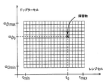
障害物を2つのどちらかの種類、すなわち特定の速度で移動する障害物と、その他の全ての障害物だけに分類する場合は、時間−周波数平面は必要なレンジセルの数に等しい数の分解能セルへと区分される。これらの分解能セルのいずれかで検出される障害物はそのセルによって特定されたレンジを有するが、その速度はドップラー周波数ωDの全間隔に対応する複数の許容速度、たとえばωDmin<ωD<ωDmaxの1つでよい。
【0040】
図8は、特定間隔のドップラー周波数について多数のレンジ分解能セルに区分された時間−周波数平面を表示している。レンジセルτoに位置する障害物は全ドップラー間隔に対応する速度間隔ωDmin<ωD<ωDmax内の半径方向速度を有している場合がある。
【0041】
特定の速度のいずれかで移動する障害物を検出するために、(1)および(2)によって与えられた2つの相関積分は下記で置換えることができる。
【数12】
【0042】
補助信号dc(t)およびds(t)は下記のように、すなわち、
−当該のドップラー周波数の全間隔をカバーする、間隔T0内の、全ての相互に直交する周波数成分を含むように、
−当該の各周波数に2つの直交成分を含み、ひいては未知の位相ずれの独立性が得られるように、
−特定値の再構成エラーについて最小限のビット数でデジタル式にアナログ波形を表現するために必要な小さい値の波高率(すなわち実効値で除算された波形の波高値)を呈するように、
−当該の周波数の全間隔にわたって平坦な周波数応答を呈し、また他の全てのドップラー周波数で必要な減衰をも伴う信号プロセッサを備えるように設計する必要がある。
【0043】
本発明の好適な実施の形態によると、2つの補助信号dc(t)およびds(t)は下記によって定義される4つの有限継続期間チャープ(chirp)、dCE(t)、dSE(t)、dCO(t)、dSO(t)を適宜に複合することによって得られる。
【数13】
【0044】
チャープdSE(t)は対応するチャープdCE(t)の直交する複製であり、同様にチャープdSO(t)は対応するチャープdCO(t)の直交する複製である。基本周波数fpの全ての調波は(uだけ)偏移され、各々が偶数または奇数調波を含む2組に分割される。次にこれらの組を利用して直交する2群のチャープ、{dCE(t)、dSE(t)}、および{dCO(t)、dSO(t)}が合成される。
【0045】
ウインドウ関数WE(t)およびWo(t)はブラックマン・ウインドウ、カイザーベッセル・ウインドウ、またはドルフチェビシェブ・ウインドウのような公知の、広範に利用されている大分類のウインドウ関数に属している。選択されたウインドウの継続期間TWは、周波数成分の直交性を活用するように選択され、またはウインドウの種類と形状は主として当該の各ドップラー周波数で必要な周波数分解能によって決定される。
【0046】
最適化手順を簡略にし、かつ対称的なチャープを得るために、位相αkおよびβkの値を2つの値、すなわち0とπだけに限定することができる。このような場合は、4つのチャープ、すなわちdCE(t)、dSE(t)、dCO(t)、dSO(t)は下記のように合成される。
【数14】
【0047】
2つの相関積分(3)および(4)の値を決定し、複合する信号プロセッサは、「ドップラーに耐性がある」信号プロセッサと呼ばれる。その結果としての広帯域のドップラー補償によってドップラーに耐性がある信号プロセッサの出力で当該の全ての障害物が検出可能(「視認可能」)になり、しかも他の全ての障害物は強力に減衰される。
【0048】
図9は、本発明による直交ドップラー発生器QDGを組み込んだ2チャネルのドップラー耐性がある信号プロセッサのブロック図である。このプロセッサは同一の2つの信号処理ブロックCRI、およびCRQを使用しており、そのいずれも従来型の相関器、またはその他の適宜の信号プロセッサでよい。以下では、ブロックCRIとCRQが各々従来型のマルチチャネル相関器であるものと想定する。
【0049】
図10は、各ブロックCRIおよびCRQの適宜な構造の例である、従来の技術によって構成された(図5を参照)マルチチャネル相関器のブロック図である。この相関器は複数のユニット遅延Δで判定された相関関数のJ個の別々の値を供給する。
【0050】
図9の2チャネルのドップラー耐性がある信号プロセッサの場合、ドップラー補償機能は直交ドップラー発生器QDG、2つのアナログ乗算器、すなわちAMIおよびAMQ、およびチャネルコンバイナIQCによって共同して実行される。
【0051】
一連の完全な動作は偶数サイクルおよび奇数サイクルと呼ばれる等しい2つのサブインターバルTWに分割された基本処理時間間隔2TWの間に2チャネル信号プロセッサによって行われる。
【0052】
図1の干渉復調器9(図9では入力信号を局部発振器信号とミキシングするためのミキサAMと、その後に配置された低域フィルタLPFとを備えているものとして図示されている)によって供給されるベースバンド信号y(t)は乗算器AMIとAMQの入力I1とQ1のそれぞれに同時に供給される。乗算器の他の2つの入力I2とQ2は直交ドップラー発生器QDGによって生成された補助信号によって励起される。
【0053】
偶数サイクル中は、発生器QDGは同時に2つのチャープを同時に、すなわち出力I2でdCE(t)を、また出力Q2でdSE(t)を発生する。奇数サイクル中、別の2つのチャープ、すなわちdCO(t)、dSO(t)がそれぞれ出力I2および出力Q2で同時に発生される。処理間隔2TWが複製される場合は、交互のサイクルはチャープdCE(t)とdCO(t)とを含み、従ってこれらが周期的な補助信号dC(t)を形成する。同様に、周期的補助信号dS(t)は複合されたチャープdSE(t)とdSO(t)の周期的な拡張によって得られる。結果として生ずるこれらの2つの直交信号dC(t)とdS(t)は各々、仮定された当該のドップラー周波数レンジ全体をカバーする同一の周波数成分を含む。
【0054】
発生器QDGは更にサイクル遷移の時点を示すパルス列EOCを発生するが、必ずしも特定の偶数または奇数サイクルではない。
【0055】
図11は、2つの補助直交信号dC(t)とdS(t)と、直交ドップラー発生器QDGによって発生されたパルス列EOCの例を示している。
【0056】
各々の相関器CRIまたはCRQは基準信号x(t)と、偶数サイクルまたは奇数サイクル中に対応する乗算器、AMIまたはAMQによって供給された信号とを一緒に処理する。各々の継続期間がTwであるこれらのサイクルはパルス列EOCの連続パルスによって始まる。偶数サイクルと奇数サイクルが終了した後に相関器CRIの出力にて示される結果はそれぞれCEおよびCOで示される。同様に、SEおよびSOは偶数サイクルと奇数サイクルがそれぞれ終了した後に相関器CRQの出力にて得られる結果を示す。
【0057】
偶数サイクル中、チャネルコンバイナIQCは、
【数15】
【数16】
【0058】
上記の表現は従来型の「ピタゴラス・プロセッサ」、または先行技術によって構成されたその他の適宜のプロセッサを使用して決定され得る。
【0059】
チャネルコンバイナIQCの構造を簡略にするため、REとROの値もある種の適宜の概算、例えば
【数17】
【0060】
所定数Lの処理間隔2TWについて決定されるREとROの表現は、例えば加算または平均によって互いに適宜に複合され、次に、その結果生じた複合された表現REOがコンバイナIQCの出力にて示される。例えば、単一の観測間隔の場合L=1であり、REO=RE+ROである。チャネルコンバイナによって行われる全ての演算は専用のデジタルプロセッサまたは標準形のプログラム可能デジタル信号プロセッサのいずれかで実行できる。
【0061】
障害物検出の目的のため、複合された表現REOは所定の決定閾値と比較されることになる。障害物の検出は、複合された表現REOの相当値だけ閾値を超えた遅延(レンジ)セルで言明される。
【0062】
図12は、チャネルコンバイナIQCによって行われる演算、およびその結果生じた決定閾値DTを用いた検出の決定の例を概略的に示す。
【0063】
図13は、ドップラー補償機能を備えた2チャネルのドップラー耐性信号プロセッサの構成の代替実施態様を示している。この場合は、直交ドップラー発生器QDGによって発生されるチャープ、すなわちdCE(t)、dSE(t)、dCO(t)、dSO(t)で乗算されるのは基準信号x(t)であり、復調された信号y(t)ではない。このような変形を除けば、プロセッサによって実行される演算と機能はすべて、図9に示した構成によって実行されるものと同一のままである。
【0064】
図14は、ドップラー補償を利用したドップラー耐性を有する信号プロセッサの更に別の構成のブロック図である。このシステムは4つのチャネル、すなわちそれぞれが独自の相関器CRIE、CRQE、CRIOまたはCRQOを備えた一対の同相チャネルおよび一対の直交チャネルを含んでいる。この場合、チャープdCE(t)、dSE(t)、dCO(t)、dSO(t)は単一のサイクルTWの間に同時に供給される。その結果、直交ドップラー発生器はこんどは相関が行われるべき間隔を示す処理間隔信号PIのための出力に加えて、4つの信号出力を有している。偶数サイクルのチャープと奇数サイクルのチャープのために付加的な別個のチャネルを使用することで、適宜に変形されたチャネルコンバイナIQCによる複合された表現REOの決定に必要な時間は半減する。
【0065】
図13に示された変形を利用することによって、図14に示した4チャネルのドップラー耐性がある信号プロセッサの別の構成を考案することも可能である。
【0066】
用途によっては、4つのチャープ、dCE(t)、dSE(t)、dCO(t)、dSO(t)が順次生成され使用される単チャネルのドップラー耐性信号プロセッサを使用することが便利な場合もある。
【0067】
ドップラー耐性信号プロセッサの上記の全ての構成、およびその他の同様の構造は、本発明によるドップラー周波数補償のための適宜の補助信号を供給するための適宜の形式の直交ドップラー発生器QDGを利用する。
【0068】
図15は、適宜の直交ドップラー発生器QDGのブロック図である。この発生器はクロック発生器CLKによって励起されるN−ビット・バイナリカウンタBCTと、2つのメモリCVMおよびSVMと、2つのバッファレジスタCBRおよびSBRと、2つのデジタル/アナログ変換器CDAおよびSDAと、トリガ回路TRGとを含む。
【0069】
直交ドップラー発生器によって実行される動作は下記のように要約できる。すなわち、自励カウンタBCTの出力の最上位ビット(MSB)は、MSB=0である場合は偶数サイクルを特定し、MSB=1である場合は奇数サイクルを特定する。MSBおよび残りの(N−1)ビットは、各メモリCVMおよびSVMの2N個のセルのアドレスを定義するために複合して利用される。メモリCVMはMSB=0であるアドレスにチャープdCE(t)のデジタル振幅標本を格納し、一方、チャープdCO(t)の標本はMSB=1であるアドレスに記憶される。同様に、メモリSVMはMSB=0であるアドレスにチャープdSE(t)のデジタル標本を格納し、一方、チャープdSO(t)の標本はMSB=1であるアドレスに記憶される。その結果、4つのチャープの各々はM個のビットをそれぞれ含む2N-1個のバイナリ語によって表され、ここで数Mは結果として生ずるチャープ標本のデジタル表現の特定の精度を得るように選択される。
【0070】
メモリCVMおよびSVMの出力に出現する連続的なデジタル語は、クロック発生器CLKの出力2で得られる適宜に遅延されたパルス列によって決定される時点で、対応するバッファレジスタCBRおよびSBRに転送される。次に、バッファレジスタCBRおよびSBR内に保存されたデジタル語はそれぞれ2つの対応するデジタル/アナログ変換器CDAおよびSDAによってアナログ標本へと変換される。その結果、変換器CDAは反復的に、チャープdCE(t)の2N-1個のアナログ標本を生成し、その後でチャープdCO(t)の2N-1個のアナログ標本を生成する。同様に、変換器SDAは反復的に、チャープdSE(t)の2N-1個のアナログ標本を生成し、その後でチャープdSO(t)の2N-1個のアナログ標本を生成する。
【0071】
トリガ回路TRGはカウンタBCTの連続的な状態の最上位ビット(MSB)の値を表すバイナリ波形のそれぞれの遷移と一致する時点で短パルスを発生する。EOCで示されるこのような短パルスのシーケンスは各々の(偶数または奇数)サイクルの始端を示すために用いられる。パルス列EOCは相関器CRIおよびCRQの積分間隔Twを定義するために、またチャネルコンバイナIQCによって行われる様々な動作を開始するために、図9および図13に示したようなドップラー耐性信号プロセッサによって利用される。
【0072】
4チャネルのドップラー耐性信号プロセッサの場合、直交ドップラー発生器は下記のように変形される。すなわち、バイナリカウンタBCTのビット数は(N−1)に低減され、連続的なカウンタ状態は、対応する4つのチャープdCE(t)、dSE(t)、dCO(t)、dSO(t)のデジタル標本を格納する4つのメモリのアドレスを決定する。次に、4つのメモリの各々の出力が適宜のバッファレジスタを介して別個のデジタル/アナログ変換器を励起する。その結果、このように変形された直交ドップラー発生器の4つの出力で4つのチャープのアナログ表現を同時に得ることができる。
【0073】
単チャネル動作に必要な直交ドップラー発生器の変形は当業者には自明であろう。
【0074】
本発明の幾つかの基本的な態様を説明するため、またその潜在的な利点を実証するため、以下の例を検討する。
【0075】
周波数成分の数K=31であり、整数周波数偏移u=4であり、従って最小周波数と最大周波数がそれぞれ6fpおよび6fp'とする。4つのチャープの各々を2048の別個の標本で表し、WE(t)=W(t)であるものと想定し、かつk=1,2,....,31である場合にαk=βkであるものと想定する。
【0076】
下記の場合に波高率が最小値を達成することが判明した。すなわち、
【数18】
上記の係数を適用した結果、(全ての成分に単に単位係数が加算された場合)波高値が31/√(31・0.5)≒7.9から僅か1.9に低減した。波高値は確実に2未満であることが望ましい。
【0078】
選択された周波数レンジにわたって平坦な周波数応答を達成し、他の全ての周波数で必要な減衰をもたらすため、離散形ウインドウ関数w(j)は、
【数19】
但し、j=0,1,...,2047の場合、m=(j−1024)/1024であり、I0(・)は変形されたベッセル関数であり、形状パラメータξは6.24である。
【0079】
4つの別個のチャープdCE(j)、dSE(j)、dCO(j)、dSO(j)の標本は、j=0,1,...,2047の場合、
【数20】
【0080】
上記のような合成されたチャープdCE(j)、dSE(j)、dCO(j)、dSO(j)はパラメータN=12、およびM=12で直交ドップラー発生器QDGによって生成可能である。
【0081】
合成されたチャープdCE(j)、dSE(j)、dCO(j)、dSO(j)は図16および図17に示されている。図示のように、チャープは様々な形式の対称性を呈し、タイミングと制御機能とをより複雑にするという代償で、こられを直交ドップラー発生器QDGのメモリを縮減するために利用できる。
【0082】
チャープdCE(j)およびdSE(j)は偶数サイクル中に相関のために利用され、その結果CEおよびSEがそれぞれ生成される。これらの結果は次に、下記のようにチャネルコンバイナIQCによって複合される。
【数21】
その結果生じた、2チャネルのドップラー耐性がある信号プロセッサの部分的な周波数応答が図18に示されている。
【0084】
同様に、チャープdCO(j)およびはdSO(j)は奇数サイクル中に相関のために利用され、その結果COおよびSOがそれぞれ生成される。これらの結果は次に下記のようにチャネルコンバイナIQCによって複合される。
【数22】
その結果生じた、2チャネルのドップラー耐性がある信号プロセッサの相補的な周波数応答が図19に示されている。
【0086】
2つの周波数応答特性は重複(加算)されて、図20に示す複合された周波数応答が生成される。図示のように、帯域外周波数の相対的な減衰は50dBを超えることがある。
【0087】
図21の複合された周波数応答のプロットは応答のリップルが当該の全ての周波数で±0.25dBを超えることがないことを明らかにしている。
【0088】
図22は変形されたカイザー・ウインドウの代わりに、j=0,1,....,2047の場合に
【数23】
【0089】
この余弦ウインドウは(ドップラー周波数がゼロである場合)、固定的な障害物に、より多くの減衰をもたらす。しかし、周波数応答は変形されたカイザー・ウインドウに対応する周波数応答ほどには平坦ではない。リップルの形状および位置は図23に示されている。
【0090】
ドップラー耐性がある信号プロセッサの上記の全ての構成では、受信信号y(t)は選択されたウインドウによって決定される不均一のエンベロープを有するチャープで乗算される。信号エネルギのこのようなロスにより、システムの検出性能は著しく低下する可能性がある。ドップラー耐性信号プロセッサで使用される様々なウインドウを吟味した結果、その形状は二乗余弦関数に近似していることが分かる。例えば、図24は、変形されたカイザー・ウインドウと二乗余弦ウインドウとはほとんど重なることを示している。このような観測と三角関数の恒等式(trigonometric identity)sin2φ+cos2φ=1は、ウインドウの使用によるロスは、受信信号がタンデム構造で動作する2つのドップラー耐性信号プロセッサによって同時に処理されればほとんど除去できることを示唆している。いずれかのプロセッサが同じチャープ集合を使用する間、複製された集合のチャープはすべてTw/2の時間だけシフトされ、但しTwはウインドウの継続期間である。
【0091】
図25は、各々が図9に従って配置された2つの2チャネル・ドップラー耐性信号プロセッサを備えたタンデム構造によって使用される2組のチャープを示している。
【0092】
より効率が高いシステムは、各々が図14に従って開発された2つの4チャネル・ドップラー耐性信号プロセッサを備えたタンデム構造を使用するであろう。
【0093】
主信号を調査するために補助信号が使用され、かつ各補助信号は他の補助信号の部分と重複する有限の継続期間を有する部分を含んでいるこの技術は、独立した発明性を有するものと見なされる。これは、本明細書に開示した特定の分野を超えた他の信号処理の分野にも応用可能であり、それには補助信号が異なる周波数成分を含む構成が含まれるが、これに限定されるものではない。更にこれを、2列以上の補助信号列の使用にも対応するように拡張することもできる。
【0094】
上記実施の形態の相関器の代わりに、WO−A−39643号に記載されているような適宜に変形された時間遅延弁別器のようなその他の装置を使用することもできよう。
【図面の簡単な説明】
【図1】 標準的なマイクロ波障害物検出システムのブロック図である。
【図2】 同期的な不規則バイナリ波形の相関関数のグラフである。
【図3】 同期的な不規則バイナリ波形の相関関数に対して目標信号のドップラーシフトの異なる位相値が及ぼす作用を示すグラフである。
【図4】 スペクトル分析器が後続する従来型の相関器のブロック図である。
【図5】 離散フーリエ変換を実施するデジタル・プロセッサが後続するマルチチャネル相関器のブロック図である。
【図6】 様々な時間遅延および様々なドップラー周波数についての相関積分の値を決定するシステムのブロック図である。
【図7】 レンジ−ドップラー分解能セルへと分割された時間−周波数平面の表示である。
【図8】 特定間隔のドップラー周波数についてレンジ分解能セルへと分割された時間−周波数平面の表示である。
【図9】 本発明による2チャネルのドップラー耐性信号プロセッサのブロック図である。
【図10】 従来技術によって構成されたマルチチャネル相関器のブロック図である。
【図11】 図9のプロセッサで使用するための信号部分の形式の補助表現の例である。
【図12】 図9のプロセッサのチャネルコンバイナによって行われる動作の例の概略図である。
【図13】 本発明による2チャネルのドップラー耐性信号プロセッサの代替実施例の構成図である。
【図14】 本発明による4チャネルのドップラー耐性信号プロセッサのブロック図である。
【図15】 本発明によるドップラー耐性信号プロセッサで使用するための直交ドップラー発生器のブロック図である。
【図16】 補助表現を構成するために使用される合成信号部分の例である。
【図17】 補助表現を構成するために使用される合成信号部分の例である。
【図18】 図16aおよびbの信号部分を使用した2チャネルのドップラー耐性信号プロセッサの部分的周波数応答を示すグラフである。
【図19】 図17aおよびbの信号部分を使用した2チャネルのドップラー耐性信号プロセッサの相補的周波数応答を示すグラフである。
【図20】 4つの信号部分の全てを使用した2チャネルのドップラー耐性信号プロセッサの複合された周波数応答を示すグラフである。
【図21】 図20の複合された周波数応答のリップルを示すグラフである。
【図22】 二乗余弦ウインドウを使用した2チャネルのドップラー耐性信号プロセッサの複合された周波数応答を示すグラフである。
【図23】 図22の複合された周波数応答のリップルを示すグラフである。
【図24】 変形されたカイザー・ウインドウ(実線)および二乗余弦ウインドウ(破線)を示すグラフである。
【図25】 タンデム構成で動作する2つの2チャネル・ドップラー耐性信号プロセッサによって使用される2組の補助信号集合AおよびBを示す図面である。[0001]
BACKGROUND OF THE INVENTION
The present invention relates to a method and apparatus for detecting a signal. In particular, the present invention provides a substantially continuous modulation modulated interfering signal used for communication and ranging purposes, particularly an irregular or disordered waveform used in obstacle detection or collision avoidance systems. The present invention is applicable to a system that is susceptible to an unknown Doppler frequency shift that affects the signal, but is not limited thereto.
[0002]
[Prior art]
Such a system is designed to operate in a multi-user environment, and often in a hostile environment, and is intended for a wide range of applications including automotive applications, industrial robots, and unmanned vehicle navigation.
[0003]
FIG. 1 is a block diagram of a standard microwave obstacle detection system. The system comprises a
[0004]
The system further includes a
[0005]
Next, the modulation waveform x (t) and its time-delayed replica y (t) are combined and processed during a specific time interval by an
[0006]
FIG. 2 shows an example of the correlation function of a synchronous irregular binary waveform.
[0007]
When relative movement occurs between the ranging system and the obstacle, the electromagnetic wave reflected from the obstacle and received by the coherent system exhibits a Doppler frequency shift. This (angular) frequency shift value ω D0 Can be calculated from:
[Expression 1]
[0008]
The signal reflected by the moving obstacle can be expressed as:
[Expression 2]
[0009]
Received signal z r The baseband signal corresponding to (t) is
[Equation 3]
[0010]
The correlator performs the following operations.
[Expression 4]
[Equation 5]
[0011]
Each duration is T 0 If the correlation integral is iteratively calculated over successive short processing intervals, the observed correlation function sequence is represented by the plot of FIG. Correlation function R xy (Τ) (time) change rate is Doppler frequency ω D0 Corresponding to This frequency value can be calculated by applying some appropriate type of spectral analysis.
[0012]
FIG. 4 is a block diagram of a conventional correlator including a
[0013]
FIG. 5 shows the total time delay interval τ assumed in J steps of the unit delay Δ using the
[0014]
The systems shown in FIGS. 4 and 5, and other similar known systems, have a number of relatively short observation intervals T 0 By combining the time sequence of the correlation function determined over the two parameters: delay time τ and topler frequency ω D Attempt to approximate the correlation integral with As a rough estimate, such a system can solve the problem of joint estimation of time delay and Doppler frequency only optimally rather than optimally.
[0015]
Other prior art includes the entire assumed time delay interval,
[Formula 6]
[Expression 7]
[Equation 8]
[0016]
FIG. 6 shows a particular time delay τ and Doppler frequency ω D It is a block diagram of an appropriate system capable of calculating a correlation integral value for. This system is formed by a correlator similar to that shown in FIG. 4, including a
[0017]
The procedure for adjusting the unknown value of phase φ is the total interval of the assumed time delay
[Equation 9]
[Expression 10]
[Expression 11]
[Problems to be solved by the invention]
In many industrial and automotive applications, systems developed by the prior art that can detect moving obstacles and utilize a nearly continuous modulated microwave (or other coherent radiation) are too complex, and Too expensive.
[0019]
In addition, obstacle detection systems designed for multi-user environments preferably have irregular or random modulations that do not require the use of conventional Doppler signal processors constructed according to the prior art. Utilize some appropriate format.
[0020]
[Means for Solving the Problems]
Aspects of the invention are set out in the accompanying claims.
[0021]
In accordance with yet another aspect of the present invention, the representation of the transmitted signal and the received signal together to determine whether a target signal exists (this target signal may represent an object that reflects the transmitted signal). It is processed. For example, an auxiliary representation formed from one or more auxiliary signals is introduced into the processing step. The auxiliary representation includes frequencies that are distributed over a range corresponding to the expected frequency modulation (such as Doppler shift) in the target signal, so that the system exhibits frequency modulation within this range. The target signal induces a significant system output, while frequency modulation outside the range has a response characteristic that does not induce this.
[0022]
Such a configuration eliminates the need to determine the value of frequency modulation (such as Doppler shift) and allows any target signal incorporating that frequency modulation to be quickly detected using a simple structure. become. Thus, the above configuration is sufficient for applications in which it is sufficient to distinguish between a fixed obstacle and an obstacle moving at a specific speed, and the obstacles are, for example, zero / slow, medium / average, fast / super It is particularly useful for applications that are classified into many grades depending on the speed of the obstacle, such as high speed.
[0023]
The preferred embodiment of the present invention relates to the nature of auxiliary expressions and provides many advantages as follows.
[0024]
Preferably, the auxiliary representation takes the form of a signal portion with a finite duration, with multiple frequencies within the range, and preferably distributed over the range. The duration of this signal portion is selected to preserve the orthogonality of the components at each frequency. By using parts with a finite duration and selecting the shape of these parts appropriately, adjacent frequencies as well as for the frequency of the target signal equal to the frequency of the signal components used to construct the auxiliary representation The response characteristics of the system can be extended so that a significant output is also generated.
[0025]
Preferably, each signal portion is created using a window function, resulting in a significant frequency response for all frequencies within that range. However, it is difficult to configure the signal portion to produce a flat response over the frequency range of interest.
[0026]
For this reason, according to a preferred embodiment of the present invention, the auxiliary representation has components each having a respective series of frequencies, each having a duration configured to induce complementary frequency response characteristics. It has a finite number of different signal parts. Thus, by combining the results achieved using different auxiliary signal portions, it is possible to obtain an overall frequency response characteristic that is significantly flatter than when only one type of signal portion is used. .
[0027]
Preferably, each signal portion includes frequency components that are interleaved with the frequency components of the other signal portion (s).
[0028]
As shown in FIG. 3, the correlation function may be at a low level depending on the phase of the Doppler shift at any given time. In order to ensure a significant output despite the unknown phase, the auxiliary representation preferably includes a first representation and a second representation, and each frequency within the first representation. The component is in quadrature relationship with the corresponding frequency component in the second representation. By combining the responses achieved as a result of these two auxiliary signals, the output is hardly affected by the phase of the Doppler shift.
[0029]
Thus, in the preferred embodiment, there are at least four types of auxiliary signal portions. That is, a signal portion that differs in that it includes a frequency subjected to frequency interleaving in another portion, and a signal portion that differs in that the frequency component is orthogonal to the frequency component in the other portion.
[0030]
Although the preferred embodiment utilizes four types of signal portions, it would be possible to construct a system that utilizes more types of signal portions and still retains the above advantages. For example, the frequency component may be divided into three or more subsets.
[0031]
It would be desirable to synthesize auxiliary representations digitally. To facilitate this, the auxiliary representation preferably exhibits a crest factor with a small value, i.e. a crest value divided by the effective value. By minimizing this value, the waveform can be digitally represented with a minimum number of bits in the event of a particular reconstruction error.
[0032]
A small crest factor can be achieved by appropriately selecting the initial phase value of the signal component for each signal portion.
[0033]
In the preferred embodiment described below, the transmitted representation and the received representation are signals combined by correlation. However, other configurations are possible. For example, the received signal can be transformed (eg, multiplied) by the auxiliary representation and then sent to a filter that is matched to the characteristics of the transmitted signal. It is well known in the art to use such a matched filter that utilizes a representation of the transmitted signal rather than the signal itself.
[0034]
In other alternative embodiments, an appropriately modified version of the time delay discriminator described in WO-A-00 / 39643, the contents of which are referred to herein, is used in place of the correlator.
[0035]
Although the invention has been described primarily in the context of detecting obstacles that cause Doppler shifts in the reflected signal, the invention is applicable in other fields. For example, the present invention can be applied to a communication system in which the local oscillators of the transmitter and the receiver are not precisely matched. A frequency offset between the oscillators will induce a frequency shift similar to a Doppler shift. Thus, the present invention allows the use of devices that have a wide tolerance and thus are cheaper than prior art configurations.
[0036]
The present invention relates to both signal processing methods and devices operating according to such methods.
[0037]
DETAILED DESCRIPTION OF THE INVENTION
Here, the structure which implemented this invention is demonstrated as an example with reference to an accompanying drawing.
[0038]
FIG. 7 displays a time-frequency plane partitioned into range-Doppler resolution cells and hypothetical obstacles that block a single cell. The conventional configuration is the cell coordinate τ o And ω D0 Designed to establish.
[0039]
When classifying obstacles into one of two types, ie, obstacles moving at a specific speed and all other obstacles, the time-frequency plane has a number of resolution cells equal to the number of range cells required. It is divided into Obstacles detected in any of these resolution cells have the range specified by that cell, but their speed is the Doppler frequency ω D Multiple permissible speeds corresponding to the total spacing of, for example ω Dmin <Ω D <Ω Dmax One of
[0040]
FIG. 8 displays a time-frequency plane partitioned into a number of range resolution cells for a particular interval of Doppler frequencies. Range cell τ o The obstacle located at is the speed interval ω corresponding to the total Doppler interval Dmin <Ω D <Ω Dmax May have a radial velocity within.
[0041]
In order to detect obstacles moving at any particular speed, the two correlation integrals given by (1) and (2) can be replaced by:
[Expression 12]
[0042]
Auxiliary signal d c (T) and d s (T) is as follows:
An interval T covering the entire interval of the relevant Doppler frequency 0 To include all mutually orthogonal frequency components in
-So that each frequency of interest contains two quadrature components, and thus the independence of an unknown phase shift is obtained,
-Exhibiting a small crest factor (ie, crest value of the waveform divided by the rms value) necessary to represent an analog waveform digitally with a minimum number of bits for a specific value reconstruction error;
-It should be designed to have a signal processor that exhibits a flat frequency response over the entire interval of the frequency of interest and also has the necessary attenuation at all other Doppler frequencies.
[0043]
According to a preferred embodiment of the invention, two auxiliary signals d c (T) and d s (T) is a four finite duration chirp defined by: d CE (T), d SE (T), d CO (T), d SO It is obtained by appropriately combining (t).
[Formula 13]
[0044]
Chirp d SE (T) is the corresponding chirp d CE An orthogonal copy of (t), similarly chirp d SO (T) is the corresponding chirp d CO It is an orthogonal copy of (t). Fundamental frequency f p Are shifted (by u) and split into two sets, each containing an even or odd harmonic. Next, using these sets, two groups of orthogonal chirps, {d CE (T), d SE (T)} and {d CO (T), d SO (T)} is synthesized.
[0045]
Window function W E (T) and W o (T) belongs to a well-known and widely used window function such as the Blackman window, Kaiser Bessel window, or Dorf Chebyshev window. Duration T of the selected window W Is selected to take advantage of the orthogonality of the frequency components, or the type and shape of the window is determined primarily by the frequency resolution required at each Doppler frequency of interest.
[0046]
To simplify the optimization procedure and obtain a symmetric chirp, the phase α k And β k Can be limited to only two values, namely 0 and π. In such a case, four chirps, d CE (T), d SE (T), d CO (T), d SO (T) is synthesized as follows.
[Expression 14]
[0047]
A signal processor that determines and combines the values of the two correlation integrals (3) and (4) is called a "Doppler-resistant" signal processor. The resulting broadband Doppler compensation makes all such obstacles detectable ("visible") at the output of the Doppler-resistant signal processor, and all other obstacles are strongly attenuated .
[0048]
FIG. 9 is a block diagram of a two channel Doppler tolerant signal processor incorporating an orthogonal Doppler generator QDG according to the present invention. The processor uses the same two signal processing blocks CRI and CRQ, both of which may be conventional correlators or other suitable signal processors. In the following, it is assumed that the blocks CRI and CRQ are each a conventional multi-channel correlator.
[0049]
FIG. 10 is a block diagram of a multi-channel correlator configured according to the prior art (see FIG. 5), which is an example of a suitable structure for each block CRI and CRQ. The correlator provides J distinct values of the correlation function determined by a plurality of unit delays Δ.
[0050]
For the two channel Doppler tolerant signal processor of FIG. 9, the Doppler compensation function is performed jointly by the quadrature Doppler generator QDG, two analog multipliers, namely AMI and AMQ, and the channel combiner IQC.
[0051]
A series of complete operations consists of two equal subintervals T called even and odd cycles. W Basic processing time interval divided by 2T W Is performed by a two-channel signal processor.
[0052]
1 provided by the interferometric demodulator 9 (shown in FIG. 9 as comprising a mixer AM for mixing the input signal with the local oscillator signal and a low-pass filter LPF disposed thereafter). The baseband signal y (t) is supplied simultaneously to the inputs I1 and Q1 of the multipliers AMI and AMQ, respectively. The other two inputs I2 and Q2 of the multiplier are excited by the auxiliary signal generated by the quadrature Doppler generator QDG.
[0053]
During even cycles, the generator QDG simultaneously produces two chirps, i.e. d at output I2. CE (T) and d at output Q2 SE (T) is generated. Two other chirps during an odd cycle, d CO (T), d SO (T) is simultaneously generated at output I2 and output Q2, respectively. Processing interval 2T W Alternate cycles are chirped d CE (T) and d CO (T) and therefore these are periodic auxiliary signals d C (T) is formed. Similarly, the periodic auxiliary signal d S (T) is the combined chirp d SE (T) and d SO Obtained by periodic expansion of (t). The resulting two quadrature signals d C (T) and d S (T) each contains the same frequency component covering the entire assumed Doppler frequency range.
[0054]
The generator QDG further generates a pulse train EOC indicating the point of cycle transition, but not necessarily a specific even or odd cycle.
[0055]
FIG. 11 shows two auxiliary quadrature signals d C (T) and d S (T) and an example of the pulse train EOC generated by the orthogonal Doppler generator QDG is shown.
[0056]
Each correlator CRI or CRQ processes the reference signal x (t) together with the signal supplied by the corresponding multiplier, AMI or AMQ during the even or odd cycle. Each duration is T w These cycles are started by successive pulses of the pulse train EOC. The results shown at the output of the correlator CRI after the even and odd cycles are finished are denoted CE and CO, respectively. Similarly, SE and SO indicate the results obtained at the output of the correlator CRQ after the even and odd cycles have been completed, respectively.
[0057]
During even cycles, the channel combiner IQC is
[Expression 15]
[Expression 16]
[0058]
The above expression may be determined using a conventional “Pythagoras processor” or other suitable processor constructed according to the prior art.
[0059]
In order to simplify the structure of the channel combiner IQC, the values of RE and RO are also some suitable approximation, eg
[Expression 17]
[0060]
Processing interval 2T of a predetermined number L W The RE and RO representations determined for are appropriately combined with each other, for example by addition or averaging, and the resulting combined representation REO is then shown at the output of the combiner IQC. For example, in the case of a single observation interval, L = 1 and REO = RE + RO. All operations performed by the channel combiner can be performed by either a dedicated digital processor or a standard programmable digital signal processor.
[0061]
For the purpose of obstacle detection, the combined representation REO will be compared to a predetermined decision threshold. Obstacle detection is asserted in a delay (range) cell that exceeds the threshold by an equivalent value of the combined representation REO.
[0062]
FIG. 12 schematically shows an example of the computation performed by the channel combiner IQC and the detection decision using the resulting decision threshold DT.
[0063]
FIG. 13 shows an alternative embodiment of a two-channel Doppler tolerant signal processor configuration with Doppler compensation. In this case, the chirp generated by the orthogonal Doppler generator QDG, i.e. d CE (T), d SE (T), d CO (T), d SO It is the reference signal x (t) that is multiplied by (t), not the demodulated signal y (t). Except for such variations, all operations and functions performed by the processor remain the same as those performed by the configuration shown in FIG.
[0064]
FIG. 14 is a block diagram of still another configuration of a signal processor having Doppler tolerance using Doppler compensation. The system includes four channels: a pair of in-phase channels and a pair of quadrature channels, each with its own correlator CRIE, CRQE, CRIO or CRQO. In this case, chirp d CE (T), d SE (T), d CO (T), d SO (T) is a single cycle T W Are supplied at the same time. As a result, the quadrature Doppler generator now has four signal outputs in addition to the output for the processing interval signal PI indicating the interval at which the correlation should be performed. By using additional separate channels for even and even cycle chirps, the time required to determine the combined representation REO by appropriately modified channel combiner IQC is halved.
[0065]
By utilizing the variation shown in FIG. 13, it is possible to devise another configuration of the signal processor with four channel Doppler tolerance shown in FIG.
[0066]
Depending on the application, 4 chirps, d CE (T), d SE (T), d CO (T), d SO It may be convenient to use a single channel Doppler tolerant signal processor in which (t) is generated and used sequentially.
[0067]
All the above configurations of the Doppler tolerant signal processor, and other similar structures, utilize a suitable type of quadrature Doppler generator QDG for providing a suitable auxiliary signal for Doppler frequency compensation according to the present invention.
[0068]
FIG. 15 is a block diagram of a suitable quadrature Doppler generator QDG. This generator comprises an N-bit binary counter BCT excited by a clock generator CLK, two memories CVM and SVM, two buffer registers CBR and SBR, two digital / analog converters CDA and SDA, Trigger circuit TRG.
[0069]
The operations performed by the orthogonal Doppler generator can be summarized as follows. That is, the most significant bit (MSB) of the output of the self-excited counter BCT specifies an even cycle when MSB = 0, and specifies an odd cycle when MSB = 1. The MSB and the remaining (N-1) bits are 2 in each memory CVM and SVM. N Used in combination to define the address of a single cell. Memory CVM is chirped at the address where MSB = 0 CE Store the digital amplitude sample of (t), while chirp d CO The sample of (t) is stored at an address where MSB = 1. Similarly, the memory SVM is chirped to the address where MSB = 0. SE Store digital sample of (t), while chirp d SO The sample of (t) is stored at an address where MSB = 1. As a result, each of the four chirps contains 2 M bits respectively. N-1 Represented by a number of binary words, the number M is chosen to obtain a particular accuracy of the digital representation of the resulting chirp sample.
[0070]
Successive digital words appearing at the outputs of the memories CVM and SVM are transferred to the corresponding buffer registers CBR and SBR at a time determined by an appropriately delayed pulse train obtained at the
[0071]
The trigger circuit TRG generates a short pulse at the time when it coincides with each transition of the binary waveform representing the value of the most significant bit (MSB) of the continuous state of the counter BCT. Such a sequence of short pulses, denoted EOC, is used to indicate the beginning of each (even or odd) cycle. The pulse train EOC is the integration interval T of the correlators CRI and CRQ. w Is used by a Doppler tolerant signal processor as shown in FIGS. 9 and 13 to define and to initiate various operations performed by the channel combiner IQC.
[0072]
For a four channel Doppler tolerant signal processor, the quadrature Doppler generator is modified as follows. That is, the number of bits of the binary counter BCT is reduced to (N−1), and the continuous counter state has four corresponding chirps d CE (T), d SE (T), d CO (T), d SO Determine the addresses of the four memories that store the digital samples of (t). Next, the output of each of the four memories excites a separate digital / analog converter via an appropriate buffer register. As a result, analog representations of four chirps can be obtained simultaneously with the four outputs of the orthogonal Doppler generator thus modified.
[0073]
Variations on the orthogonal Doppler generator required for single channel operation will be apparent to those skilled in the art.
[0074]
To illustrate some basic aspects of the present invention and to demonstrate its potential advantages, consider the following example.
[0075]
The number of frequency components K = 31 and the integer frequency deviation u = 4, so that the minimum frequency and the maximum frequency are 6f respectively. p And 6f p ' And Each of the four chirps is represented by 2048 separate samples and W E (T) = W (t) and k = 1, 2,. . . . , 31 k = Β k Assuming that
[0076]
It was found that the crest factor achieved the minimum value in the following cases. That is,
[Formula 18]
As a result of applying the above coefficients, the crest value was reduced from 31 / √ (31 · 0.5) ≈7.9 to only 1.9 (when unit coefficients were simply added to all components). It is desirable that the peak value is surely less than 2.
[0078]
In order to achieve a flat frequency response over the selected frequency range and provide the necessary attenuation at all other frequencies, the discrete window function w (j) is
[Equation 19]
However, j = 0, 1,. . . , 2047, m = (j−1024) / 1024, and I 0 (•) is a modified Bessel function, and the shape parameter ξ is 6.24.
[0079]
4 separate chirps d CE (J), d SE (J), d CO (J), d SO The sample of (j) is j = 0, 1,. . . , 2047,
[Expression 20]
[0080]
The synthesized chirp d as above CE (J), d SE (J), d CO (J), d SO (J) can be generated by the orthogonal Doppler generator QDG with parameters N = 12, and M = 12.
[0081]
Synthesized chirp d CE (J), d SE (J), d CO (J), d SO (J) is shown in FIG. 16 and FIG. As shown, the chirp exhibits various forms of symmetry, and can be used to reduce the memory of the quadrature Doppler generator QDG at the cost of more complex timing and control functions.
[0082]
Chirp d CE (J) and d SE (J) is used for correlation during even cycles, resulting in CE and SE, respectively. These results are then combined by the channel combiner IQC as follows:
[Expression 21]
The resulting partial frequency response of a 2-channel Doppler tolerant signal processor is shown in FIG.
[0084]
Similarly, chirp d CO (J) and d SO (J) is used for correlation during odd cycles, resulting in CO and SO, respectively. These results are then combined by the channel combiner IQC as follows:
[Expression 22]
The resulting complementary frequency response of a two channel Doppler tolerant signal processor is shown in FIG.
[0086]
The two frequency response characteristics are overlapped (added) to generate the combined frequency response shown in FIG. As shown, the relative attenuation of out-of-band frequencies can exceed 50 dB.
[0087]
The combined frequency response plot of FIG. 21 reveals that the response ripple does not exceed ± 0.25 dB at all frequencies of interest.
[0088]
FIG. 22 shows j = 0, 1,... Instead of the modified Kaiser window. . . . , 2047
[Expression 23]
[0089]
This cosine window (when the Doppler frequency is zero) provides more attenuation to the fixed obstacle. However, the frequency response is not as flat as the frequency response corresponding to the deformed Kaiser window. The shape and position of the ripple is shown in FIG.
[0090]
In all of the above configurations of Doppler tolerant signal processors, the received signal y (t) is multiplied by a chirp with a non-uniform envelope determined by the selected window. Such loss of signal energy can significantly reduce the detection performance of the system. Examination of the various windows used in the Doppler tolerant signal processor shows that its shape approximates a raised cosine function. For example, FIG. 24 shows that the modified Kaiser window and the raised cosine window almost overlap. Such observations and trigonometric identity sin 2 φ + cos 2 φ = 1 suggests that the loss due to the use of the window can be almost eliminated if the received signal is processed simultaneously by two Doppler tolerant signal processors operating in a tandem structure. While any processor uses the same chirp set, the chirps of the replicated set are all T w Shifted by the time of / 2, where T w Is the duration of the window.
[0091]
FIG. 25 shows two sets of chirps used by a tandem structure with two 2-channel Doppler tolerant signal processors, each arranged according to FIG.
[0092]
A more efficient system would use a tandem structure with two 4-channel Doppler tolerant signal processors each developed according to FIG.
[0093]
This technique, in which an auxiliary signal is used to examine the main signal, and each auxiliary signal includes a portion having a finite duration that overlaps with other auxiliary signal portions, has independent inventiveness. Considered. This is applicable to other signal processing fields beyond the specific fields disclosed herein, including but not limited to configurations where the auxiliary signal contains different frequency components. is not. Furthermore, this can be extended to accommodate the use of two or more auxiliary signal sequences.
[0094]
Instead of the correlator of the above embodiment, other devices such as a suitably modified time delay discriminator as described in WO-A-39643 could be used.
[Brief description of the drawings]
FIG. 1 is a block diagram of a standard microwave obstacle detection system.
FIG. 2 is a graph of a correlation function of a synchronous irregular binary waveform.
FIG. 3 is a graph showing the effect of different phase values of the Doppler shift of the target signal on the correlation function of a synchronous irregular binary waveform.
FIG. 4 is a block diagram of a conventional correlator followed by a spectrum analyzer.
FIG. 5 is a block diagram of a multi-channel correlator followed by a digital processor that performs a discrete Fourier transform.
FIG. 6 is a block diagram of a system for determining correlation integral values for various time delays and various Doppler frequencies.
FIG. 7 is a representation of a time-frequency plane divided into range-Doppler resolution cells.
FIG. 8 is a representation of a time-frequency plane divided into range resolution cells for specific intervals of Doppler frequencies.
FIG. 9 is a block diagram of a two-channel Doppler tolerant signal processor according to the present invention.
FIG. 10 is a block diagram of a multi-channel correlator configured according to the prior art.
FIG. 11 is an example of an auxiliary representation in the form of a signal portion for use in the processor of FIG.
12 is a schematic diagram of an example of operations performed by the channel combiner of the processor of FIG.
FIG. 13 is a block diagram of an alternative embodiment of a two-channel Doppler tolerant signal processor according to the present invention.
FIG. 14 is a block diagram of a four channel Doppler tolerant signal processor in accordance with the present invention.
FIG. 15 is a block diagram of an orthogonal Doppler generator for use in a Doppler tolerant signal processor according to the present invention.
FIG. 16 is an example of a composite signal portion used to construct an auxiliary representation.
FIG. 17 is an example of a composite signal portion used to construct an auxiliary representation.
FIG. 18 is a graph showing the partial frequency response of a two channel Doppler tolerant signal processor using the signal portion of FIGS. 16a and b.
FIG. 19 is a graph showing the complementary frequency response of a two-channel Doppler tolerant signal processor using the signal portion of FIGS. 17a and b.
FIG. 20 is a graph showing the combined frequency response of a two channel Doppler tolerant signal processor using all four signal portions.
21 is a graph showing ripple of the combined frequency response of FIG.
FIG. 22 is a graph showing the combined frequency response of a two channel Doppler tolerant signal processor using a raised cosine window.
FIG. 23 is a graph showing ripple of the combined frequency response of FIG.
FIG. 24 is a graph showing a modified Kaiser window (solid line) and a raised cosine window (dashed line).
FIG. 25 shows two sets of auxiliary signals A and B used by two 2-channel Doppler tolerant signal processors operating in a tandem configuration.
Claims (21)
前記補助表現が前記目標信号内で可能なドップラーシフトに対応する周波数レンジ内の異なる周波数の複数の同時発生する成分を有するマルチ周波数信号から構成されることによって、1つの前記周波数に対応するドップラーシフトを示す受信信号は前記複合の結果に有意性応答をもたらすことを特徴とする方法。After transforming one of the main representation of the transmission signal and the main representation of the reception signal using the auxiliary representation, the main representation of the transmission signal and the main representation of the reception signal are combined, and the composite result A method for detecting a target signal comprising determining whether a target signal exists from
Doppler shift corresponding to one said frequency by said auxiliary representation being composed of multi-frequency signals having a plurality of simultaneously occurring components of different frequencies within the frequency range corresponding to possible Doppler shifts in said target signal A received signal indicative of wherein the combined result provides a significant response to the combined result.
前記補助表現が前記送信信号と前記受信信号との間に生じ得る周波数の不一致に対応する周波数レンジ内の異なる周波数の複数の同時発生する成分を有するマルチ周波数信号から構成されることによって、1つの前記周波数に対応する不一致を示す受信信号は前記複合の結果に有意性応答をもたらすことを特徴とする方法。After transforming one of the main expression of the transmission signal and the main expression of the reception signal using the auxiliary expression, the main expression of the transmission signal and the main expression of the reception signal are combined, and the target is obtained from the result of the combination A method for detecting a target signal comprising determining whether a signal is present, comprising:
The auxiliary representation is composed of a multi-frequency signal having a plurality of co-occurring components of different frequencies within a frequency range corresponding to a frequency mismatch that may occur between the transmitted signal and the received signal; A received signal that exhibits a mismatch corresponding to the frequency provides a significant response to the composite result.
Applications Claiming Priority (2)
| Application Number | Priority Date | Filing Date | Title |
|---|---|---|---|
| EP01303183A EP1248119B1 (en) | 2001-04-03 | 2001-04-03 | Method and Apparatus for Detecting a Target Signal and Obstacle Detection System |
| EP01303183.6 | 2001-04-03 |
Related Child Applications (1)
| Application Number | Title | Priority Date | Filing Date |
|---|---|---|---|
| JP2008199969A Division JP4448184B2 (en) | 2001-04-03 | 2008-08-01 | Signal processing method |
Publications (2)
| Publication Number | Publication Date |
|---|---|
| JP2003004842A JP2003004842A (en) | 2003-01-08 |
| JP4249428B2 true JP4249428B2 (en) | 2009-04-02 |
Family
ID=8181875
Family Applications (2)
| Application Number | Title | Priority Date | Filing Date |
|---|---|---|---|
| JP2002101445A Expired - Fee Related JP4249428B2 (en) | 2001-04-03 | 2002-04-03 | Signal detection apparatus and detection method |
| JP2008199969A Expired - Fee Related JP4448184B2 (en) | 2001-04-03 | 2008-08-01 | Signal processing method |
Family Applications After (1)
| Application Number | Title | Priority Date | Filing Date |
|---|---|---|---|
| JP2008199969A Expired - Fee Related JP4448184B2 (en) | 2001-04-03 | 2008-08-01 | Signal processing method |
Country Status (4)
| Country | Link |
|---|---|
| US (2) | US6753803B2 (en) |
| EP (2) | EP1610150B1 (en) |
| JP (2) | JP4249428B2 (en) |
| DE (1) | DE60114561T2 (en) |
Families Citing this family (17)
| Publication number | Priority date | Publication date | Assignee | Title |
|---|---|---|---|---|
| JP4283170B2 (en) * | 2003-12-17 | 2009-06-24 | 株式会社デンソー | Object detection device |
| US11152971B2 (en) * | 2004-02-02 | 2021-10-19 | Charles Abraham | Frequency modulated OFDM over various communication media |
| US7528764B2 (en) * | 2004-09-14 | 2009-05-05 | Bae Systems Information And Electronic Systems Integration Inc. | Through the wall ranging with triangulation using multiple spaced apart radars |
| US7355545B2 (en) * | 2004-11-02 | 2008-04-08 | Bae Systems Information And Electronic Systems Integration Inc. | Through the wall ranging with triangulation using multiple spaced apart radars |
| US7812760B2 (en) | 2006-04-20 | 2010-10-12 | Anritsu Corporation | Short-range radar and control method thereof |
| JP2008101997A (en) * | 2006-10-18 | 2008-05-01 | Mitsubishi Electric Corp | Radar system |
| EP1925949A1 (en) * | 2006-11-24 | 2008-05-28 | BP Shipping Limited | Ship mounted underwater sonar system |
| GB2452736A (en) * | 2007-09-12 | 2009-03-18 | Mitsubishi Electric Inf Tech | Determining time shift between signals |
| US8353903B2 (en) * | 2009-05-06 | 2013-01-15 | Vivant Medical, Inc. | Power-stage antenna integrated system |
| EP2278355A1 (en) | 2009-06-30 | 2011-01-26 | Mitsubishi Electric R & D Centre Europe B.V. | Radar system |
| DE102010044742A1 (en) * | 2010-09-08 | 2012-03-08 | Atlas Elektronik Gmbh | Method and apparatus for determining a Doppler frequency shift resulting from the Doppler effect |
| WO2012077345A1 (en) * | 2010-12-10 | 2012-06-14 | 三菱電機株式会社 | Monitoring device |
| CN103269259B (en) * | 2013-05-23 | 2016-09-21 | 小米科技有限责任公司 | A kind of signal demodulating method and device |
| DE102013211846A1 (en) | 2013-06-21 | 2014-12-24 | Robert Bosch Gmbh | Method for operating an environment detection system of a vehicle |
| US20180011190A1 (en) * | 2016-07-05 | 2018-01-11 | Navico Holding As | High Ping Rate Sonar |
| RU2622888C1 (en) * | 2016-08-18 | 2017-06-21 | Георгий Галиуллович Валеев | Method of identification of objectives (versions) |
| JP6696575B2 (en) | 2016-08-26 | 2020-05-20 | 日本電気株式会社 | Moving target detecting system and moving target detecting method |
Family Cites Families (14)
| Publication number | Priority date | Publication date | Assignee | Title |
|---|---|---|---|---|
| US5786788A (en) * | 1996-10-08 | 1998-07-28 | Raytheon Company | Radar system and method for reducing range sidelobes |
| US5173706A (en) * | 1991-04-16 | 1992-12-22 | General Electric Company | Radar processor with range sidelobe reduction following doppler filtering |
| US5414428A (en) * | 1993-08-06 | 1995-05-09 | Martin Marietta Corp. | Radar system with pulse compression and range sidelobe suppression preceding doppler filtering |
| US6356607B1 (en) * | 1995-06-05 | 2002-03-12 | Omnipoint Corporation | Preamble code structure and detection method and apparatus |
| JP3859716B2 (en) * | 1995-08-16 | 2006-12-20 | コーニンクレッカ フィリップス エレクトロニクス エヌ ヴィ | Transmission system |
| DE19644686A1 (en) * | 1996-10-28 | 1998-04-30 | Bosch Gmbh Robert | Calibration procedures and arrangement |
| US5867117A (en) * | 1996-12-13 | 1999-02-02 | The University Of Kansas, Center For Research, Incorporated | Swept-step radar system and detection method using same |
| US6323913B1 (en) * | 1997-01-10 | 2001-11-27 | Infineon Technologies Ag | Circuit configuration for color decoding and decimation for a video signal |
| US6427012B1 (en) * | 1997-05-19 | 2002-07-30 | Verance Corporation | Apparatus and method for embedding and extracting information in analog signals using replica modulation |
| EP0942294A3 (en) * | 1998-03-09 | 2000-06-07 | Siemens Schweiz AG (Siemens Suisse SA) (Siemens Svizzera SA) Siemens Switzerland Ltd) | Method for the reduction of the sidelobes and amplitude or phase monopulse apparatus |
| FI106656B (en) * | 1998-03-26 | 2001-03-15 | Markku Sakari Lehtinen | Method and arrangement for measuring radar reflectance and Doppler offset with a pulse radar |
| DE19854167C2 (en) * | 1998-11-24 | 2000-09-28 | Siemens Ag | Frequency-stabilized transmission / reception circuit |
| GB9828693D0 (en) | 1998-12-24 | 1999-02-17 | Mitsubishi Electric Inf Tech | Time delay determination |
| JP3759333B2 (en) * | 1999-05-28 | 2006-03-22 | 三菱電機株式会社 | Pulse Doppler radar device |
-
2001
- 2001-04-03 DE DE60114561T patent/DE60114561T2/en not_active Expired - Lifetime
- 2001-04-03 EP EP05076757.3A patent/EP1610150B1/en not_active Expired - Lifetime
- 2001-04-03 EP EP01303183A patent/EP1248119B1/en not_active Expired - Lifetime
-
2002
- 2002-04-02 US US10/112,873 patent/US6753803B2/en not_active Expired - Fee Related
- 2002-04-03 JP JP2002101445A patent/JP4249428B2/en not_active Expired - Fee Related
-
2004
- 2004-01-21 US US10/760,462 patent/US7151477B2/en not_active Expired - Fee Related
-
2008
- 2008-08-01 JP JP2008199969A patent/JP4448184B2/en not_active Expired - Fee Related
Also Published As
| Publication number | Publication date |
|---|---|
| US6753803B2 (en) | 2004-06-22 |
| EP1248119B1 (en) | 2005-11-02 |
| EP1610150A3 (en) | 2008-06-04 |
| EP1248119A1 (en) | 2002-10-09 |
| DE60114561D1 (en) | 2005-12-08 |
| US20040151067A1 (en) | 2004-08-05 |
| EP1610150B1 (en) | 2016-06-22 |
| US20020186161A1 (en) | 2002-12-12 |
| JP2003004842A (en) | 2003-01-08 |
| US7151477B2 (en) | 2006-12-19 |
| JP4448184B2 (en) | 2010-04-07 |
| DE60114561T2 (en) | 2006-08-10 |
| EP1610150A2 (en) | 2005-12-28 |
| JP2008292502A (en) | 2008-12-04 |
Similar Documents
| Publication | Publication Date | Title |
|---|---|---|
| JP4448184B2 (en) | Signal processing method | |
| TWI821290B (en) | Combined radar and communications system using common signal waveform | |
| EP3835810B1 (en) | Method and system for frequency offset modulation range division mimo automotive radar | |
| US10142133B2 (en) | Successive signal interference mitigation | |
| US7564400B2 (en) | Spread spectrum radar apparatus | |
| US10613195B2 (en) | Radar apparatus and radar method | |
| CN106796282B (en) | Radar system and method for determining range, relative velocity and bearing of object using continuous wave and chirp signals | |
| JP4462574B2 (en) | System and method for processing wideband pre-detection signals for passive coherent search applications | |
| JP6432221B2 (en) | Radar equipment | |
| EP2600170A1 (en) | Radar apparatus | |
| JP4834370B2 (en) | Correlation reception processing device | |
| JP2017167117A (en) | Radar device and positioning method | |
| CN111551925B (en) | Target speed estimation method of pulse-to-pulse frequency agility radar based on FFT | |
| Zheng et al. | Radar detection and motion parameters estimation of maneuvering target based on the extended keystone transform (July 2018) | |
| JP2014081311A (en) | Radar system | |
| JP2002040120A (en) | Position-detecting system for radio wave source | |
| CN111505571A (en) | Method and apparatus for determining the position of an object using radio frequency signals | |
| CN112965067A (en) | Target speed expanding method suitable for FMCW automobile radar | |
| CN114460595A (en) | Target measuring method, device, measuring equipment and storage medium | |
| US20040047236A1 (en) | Inteferometric synthetic sonar antenna | |
| JP2019120613A (en) | Rader system, method of controlling rader system, and program | |
| TWI771103B (en) | Radar apparatus and signal receiving method thereof | |
| GB2329072A (en) | Processing of signals incident on an array | |
| CN116886485A (en) | Communication perception integrated method, system, device and medium based on LoRa signal | |
| JP2022157184A (en) | Object detection unit |
Legal Events
| Date | Code | Title | Description |
|---|---|---|---|
| A621 | Written request for application examination |
Free format text: JAPANESE INTERMEDIATE CODE: A621 Effective date: 20050307 |
|
| A131 | Notification of reasons for refusal |
Free format text: JAPANESE INTERMEDIATE CODE: A131 Effective date: 20080205 |
|
| A601 | Written request for extension of time |
Free format text: JAPANESE INTERMEDIATE CODE: A601 Effective date: 20080507 |
|
| A602 | Written permission of extension of time |
Free format text: JAPANESE INTERMEDIATE CODE: A602 Effective date: 20080512 |
|
| A601 | Written request for extension of time |
Free format text: JAPANESE INTERMEDIATE CODE: A601 Effective date: 20080605 |
|
| A602 | Written permission of extension of time |
Free format text: JAPANESE INTERMEDIATE CODE: A602 Effective date: 20080612 |
|
| A601 | Written request for extension of time |
Free format text: JAPANESE INTERMEDIATE CODE: A601 Effective date: 20080704 |
|
| A602 | Written permission of extension of time |
Free format text: JAPANESE INTERMEDIATE CODE: A602 Effective date: 20080709 |
|
| A521 | Written amendment |
Free format text: JAPANESE INTERMEDIATE CODE: A523 Effective date: 20080801 |
|
| TRDD | Decision of grant or rejection written | ||
| A01 | Written decision to grant a patent or to grant a registration (utility model) |
Free format text: JAPANESE INTERMEDIATE CODE: A01 Effective date: 20081216 |
|
| A01 | Written decision to grant a patent or to grant a registration (utility model) |
Free format text: JAPANESE INTERMEDIATE CODE: A01 |
|
| A61 | First payment of annual fees (during grant procedure) |
Free format text: JAPANESE INTERMEDIATE CODE: A61 Effective date: 20090115 |
|
| FPAY | Renewal fee payment (event date is renewal date of database) |
Free format text: PAYMENT UNTIL: 20120123 Year of fee payment: 3 |
|
| R150 | Certificate of patent or registration of utility model |
Free format text: JAPANESE INTERMEDIATE CODE: R150 |
|
| FPAY | Renewal fee payment (event date is renewal date of database) |
Free format text: PAYMENT UNTIL: 20120123 Year of fee payment: 3 |
|
| S111 | Request for change of ownership or part of ownership |
Free format text: JAPANESE INTERMEDIATE CODE: R313113 |
|
| S631 | Written request for registration of reclamation of domicile |
Free format text: JAPANESE INTERMEDIATE CODE: R313631 |
|
| FPAY | Renewal fee payment (event date is renewal date of database) |
Free format text: PAYMENT UNTIL: 20120123 Year of fee payment: 3 |
|
| R360 | Written notification for declining of transfer of rights |
Free format text: JAPANESE INTERMEDIATE CODE: R360 |
|
| FPAY | Renewal fee payment (event date is renewal date of database) |
Free format text: PAYMENT UNTIL: 20120123 Year of fee payment: 3 |
|
| S111 | Request for change of ownership or part of ownership |
Free format text: JAPANESE INTERMEDIATE CODE: R313113 |
|
| S631 | Written request for registration of reclamation of domicile |
Free format text: JAPANESE INTERMEDIATE CODE: R313631 |
|
| S633 | Written request for registration of reclamation of name |
Free format text: JAPANESE INTERMEDIATE CODE: R313633 |
|
| FPAY | Renewal fee payment (event date is renewal date of database) |
Free format text: PAYMENT UNTIL: 20120123 Year of fee payment: 3 |
|
| R360 | Written notification for declining of transfer of rights |
Free format text: JAPANESE INTERMEDIATE CODE: R360 |
|
| FPAY | Renewal fee payment (event date is renewal date of database) |
Free format text: PAYMENT UNTIL: 20120123 Year of fee payment: 3 |
|
| R370 | Written measure of declining of transfer procedure |
Free format text: JAPANESE INTERMEDIATE CODE: R370 |
|
| FPAY | Renewal fee payment (event date is renewal date of database) |
Free format text: PAYMENT UNTIL: 20120123 Year of fee payment: 3 |
|
| S111 | Request for change of ownership or part of ownership |
Free format text: JAPANESE INTERMEDIATE CODE: R313113 |
|
| S631 | Written request for registration of reclamation of domicile |
Free format text: JAPANESE INTERMEDIATE CODE: R313631 |
|
| S633 | Written request for registration of reclamation of name |
Free format text: JAPANESE INTERMEDIATE CODE: R313633 |
|
| FPAY | Renewal fee payment (event date is renewal date of database) |
Free format text: PAYMENT UNTIL: 20120123 Year of fee payment: 3 |
|
| R350 | Written notification of registration of transfer |
Free format text: JAPANESE INTERMEDIATE CODE: R350 |
|
| FPAY | Renewal fee payment (event date is renewal date of database) |
Free format text: PAYMENT UNTIL: 20130123 Year of fee payment: 4 |
|
| FPAY | Renewal fee payment (event date is renewal date of database) |
Free format text: PAYMENT UNTIL: 20130123 Year of fee payment: 4 |
|
| FPAY | Renewal fee payment (event date is renewal date of database) |
Free format text: PAYMENT UNTIL: 20130123 Year of fee payment: 4 |
|
| FPAY | Renewal fee payment (event date is renewal date of database) |
Free format text: PAYMENT UNTIL: 20130123 Year of fee payment: 4 |
|
| LAPS | Cancellation because of no payment of annual fees |